Embed Size (px)
Citation preview

Design of Silicon Photonic Multimode Interference
Couplers
By
Andrés Sosa
Tutor: Dr. Tolga Tekin
TU Berlin
Research Center of Microperipheric Technologies
Supervisor: Jaume Comellas
UPC (Universitat Politècnica de Catalunya)
Escola Tècnica Superior d'Enginyeria de Telecomunicació de Barcelona
ETSETB
Berlin (Germany)
January 2012 - August 2012


Abstract
RSoft Design is a software used by researchers, system integrators, manufacturers and serviceproviders, thanks to its tools which provide a wide range of applications, from the design ofphotonic components to planning and design of systems and networks. Regarding the design ofphotonic components it is possible to model active and passive components, for both purposesthere is a Device Suit, and each one includes a CAD environment, simulation engines with onewith a di�erent calculation method, and an optimization utility.
The targeted photonic component to be designed was the MMI Coupler, that follows the self-imaging principle of multimodal waveguides, the application of this kind of devices has grown dueto the interest of its e�ects in integrated optics and its advantages, this component speci�callyo�ers higher fabrication tolerances and polarization independent results, both features of greatconvenience regarding the di�erent applications of this component in integrated circuits.
The MMI Coupler falls into the category of a passive photonic component, and from theseries of engines which could be applied, the BeamPROP engine, based on the Beam PropagationMethod, is implemented for its accuracy in the �nal results of the simulations, and its outstandingcomputational performance.
The design of the Coupler was based on the Fraunhofer IZM model for waveguides, whichis a SOI structure with speci�c standard dimensions, and as simulations were performed partic-ular geometric characteristics, were implemented to obtain an optimized result. The geometriccharacteristics mentioned before are the choosing of an appropriate width for the MMI sectionwhich resulted in the best possible output, the tapering of the access segments between the MMIsection and the monomode waveguides to create a better balance between the di�erent outputsand to obtain a higher power in the same point, and �nally, when necessary the tapering of theMMI section to avoid cross-talk between the monomode segments after the coupling section.
i


Resumen
RSoft Design es un software usado por investigadores, integradores de sistemas, fabricantes yproveedores de servicios, gracias a sus herramientas que ofrecen un rango considerablementeamplio de aplicaciones, desde el diseño de componentes fotónicos hasta la plani�cación y diseñode sistemas y redes. En lo referente a el diseño de componentes fotónicos es posible modelarcomponentes activos y componentes pasivos, y en ambos casos se puede contar con un Device Suit,un medio CAD, motores de simulación, cada uno con diversos métodos de cálculo, y utilidadesde optimización.
El componente fotónico a ser diseñado fue el acoplador de Interferencia Multimodal, quesigue los principios de autoimagen característicos de las guías de onda multimodal, la aplicaciónde estos dispositivos ha aumentado enormemente debido al interés de sus efectos en las ópticasintegradas y sus ventajas, este componente ofrece especí�camente una tolerancia de fabricaciónconsideráblemente elevada y resultados que son independientes de la polarización usada, ambascaracterísticas convenientes en la aplicación de éste componente en ciruitos integrados.
El acoplador antes mencionado se encuentra categorizado como un componente fotónicopasivo, y de la serie de motores utilizables para estos modelos, el motor BeamPROP, basado enel Método de Propagación del Haz, es implementado, por su precisión en los resultados �nalesde las simulaciones y por el excepcional rendimiento compucional que presenta.
El diseño del acoplador se basó en el modelo de guia de ondas de Fraunhofer IZM, el cuales una estructura SOI con dimensiones estándares especí�cos, y al llevar a cabo numerosassimulaciones fueron introducidas ciertas particularidades geométricas para obtener resultadosoptimizados. Las características geométricas mencionadas previamente fueron, la escogenciade una anchura apropiada para la sección MMI que produjese el mejor resultado posible, ladisminución o aumento gradual de los segmentos de entrada, entre la sección MMI y las guíasde onda monomodo para así crear un mejor balance entre las diferentes salidas y asi obtener enel mismo punto una potencia más elevada, y �nalmente, cuando fuese necesario la disminucióno aumento gradual de la sección MMI para evitar diafonía entre los segmentos monomodo luegodel sector de acoplamiento.
iii


Resum
RSoft Design ès un programari usat per investigadors, integradors de sistemes, fabricants iproveïdors de serveis, gràcies a les seves eines que ofereixen un rang considerablement amplid'aplicacions, des del disseny de components fotònics �ns a la plani�cació i disseny de sistemesi xarxes. Pel que fa a el disseny de components fotònics és possible modelar components actiusi components passius, i en ambdós casos es pot comptar amb un Device Suit, un mitjà CAD,motors de simulació, cadascun amb diversos mètodes de càlcul, i utilitats d'optimització.
El component fotònic a ser dissenyat va ser el acoblador d'Interferència Multimodal, quesegueix els principis de autoimatge característics de les guies d'ona multimodal, l'aplicaciód'aquests dispositius ha augmentat enormement causa de l'interès dels seus efectes en les òptiquesintegrades i les seves avantatges, aquest component ofereix especi�cament una tolerància de fab-ricació considerablement elevada i resultats que són independents de la polarització utilitzada,ambdues característiques convenients en l'aplicació d'aquest component en circuits integrats.
L'acoblador abans esmentat està categoritzat com un component fotònic passiu, i de lasèrie de motors utilitzables per aquests models, el motor BeamPROP, basat en el Mètode dePropagació del Feix, és implementat, pel seu precisió en els resultats nals de les simulacions i perl'excepcional rendiment compucional que presenta.
El disseny del acoblador es va basar en el model de guia d'ones de Fraunhofer IZM, el qualés una estructura SOI amb dimensions estàndards especí�ques, i en dur a terme nombroses simu-lacions van ser introduïdes certes particularitats geomètriques per obtenir resultats optimitzats.Les característiques geomètriques esmentades prèviament van ser la tria d'una amplada apropi-ada per a la secció MMI que produís el millor resultat possible, la disminució o augment gradualdels segments d'entrada, entre la secció MMI i les guies d'ona monomode per així crear un millorbalanç entre les diferents sortides i així obtenir en el mateix punt una potència més elevada, inalment, quan fos necessari la disminució o augment gradual de la secció MMI per evitar diafoniaentre els segments monomode després del sector d'acoblament.
v


Contents
Abstract i
Resumen iii
Resum v
List of Figures xi
List of Tables xv
Acknowledgements xxi
1 Introduction 1
1.1 Background and Scope . . . . . . . . . . . . . . . . . . . . . . . . . . . . . . . . . 2
1.1.1 Background . . . . . . . . . . . . . . . . . . . . . . . . . . . . . . . . . . . 2
1.1.2 Related Work . . . . . . . . . . . . . . . . . . . . . . . . . . . . . . . . . . 2
1.1.3 Scope . . . . . . . . . . . . . . . . . . . . . . . . . . . . . . . . . . . . . . 2
1.2 Objectives . . . . . . . . . . . . . . . . . . . . . . . . . . . . . . . . . . . . . . . . 3
1.3 Chapter Overview . . . . . . . . . . . . . . . . . . . . . . . . . . . . . . . . . . . 3
vii

2 Optical Waveguides 5
2.1 Waveguide Concepts . . . . . . . . . . . . . . . . . . . . . . . . . . . . . . . . . . 5
2.1.1 Waveguide Parameters . . . . . . . . . . . . . . . . . . . . . . . . . . . . . 6
2.1.2 Guided Modes Formation . . . . . . . . . . . . . . . . . . . . . . . . . . . 8
2.1.3 Maxwell′s Equations . . . . . . . . . . . . . . . . . . . . . . . . . . . . . . 8
2.2 Planar Waveguides . . . . . . . . . . . . . . . . . . . . . . . . . . . . . . . . . . . 10
2.2.1 Slab Waveguides . . . . . . . . . . . . . . . . . . . . . . . . . . . . . . . . 10
2.2.2 Rectangular Waveguides . . . . . . . . . . . . . . . . . . . . . . . . . . . . 12
3 Coupled Mode Theory 17
3.1 Coupled Mode Equations . . . . . . . . . . . . . . . . . . . . . . . . . . . . . . . 17
3.1.1 TE Modes . . . . . . . . . . . . . . . . . . . . . . . . . . . . . . . . . . . . 17
3.1.2 TM Modes . . . . . . . . . . . . . . . . . . . . . . . . . . . . . . . . . . . 19
3.1.3 The Coupling Equation . . . . . . . . . . . . . . . . . . . . . . . . . . . . 20
4 MMI Self-Imaging Model 21
4.1 MultiMode Waveguides . . . . . . . . . . . . . . . . . . . . . . . . . . . . . . . . 21
4.1.1 Propagation Constants . . . . . . . . . . . . . . . . . . . . . . . . . . . . . 21
4.1.2 Guided Mode Propagation Analysis . . . . . . . . . . . . . . . . . . . . . 23
4.2 General Interference . . . . . . . . . . . . . . . . . . . . . . . . . . . . . . . . . . 24
4.2.1 Single Images . . . . . . . . . . . . . . . . . . . . . . . . . . . . . . . . . . 24
4.2.2 Multiple Images . . . . . . . . . . . . . . . . . . . . . . . . . . . . . . . . 25
4.3 Restricted Interference . . . . . . . . . . . . . . . . . . . . . . . . . . . . . . . . . 27
4.3.1 Paired Interference . . . . . . . . . . . . . . . . . . . . . . . . . . . . . . . 27
4.3.2 Symmetric Interference . . . . . . . . . . . . . . . . . . . . . . . . . . . . . 28
5 Fabrication Techniques 31
5.1 Silicon-on-Insulator (SOI) . . . . . . . . . . . . . . . . . . . . . . . . . . . . . . . 31
5.1.1 SIMOX . . . . . . . . . . . . . . . . . . . . . . . . . . . . . . . . . . . . . 32
5.1.2 BESOI . . . . . . . . . . . . . . . . . . . . . . . . . . . . . . . . . . . . . . 32

5.1.3 Wafer Splitting (SmartCut Process to produce Unibond Wafers) . . . . . 35
5.1.4 Silicon Epitaxial Growth . . . . . . . . . . . . . . . . . . . . . . . . . . . . 35
5.2 Fabrication of Surface Etched Features . . . . . . . . . . . . . . . . . . . . . . . . 37
5.2.1 Photolithography . . . . . . . . . . . . . . . . . . . . . . . . . . . . . . . . 37
5.2.2 Silicon Etching . . . . . . . . . . . . . . . . . . . . . . . . . . . . . . . . . 40
5.2.3 Critical Dimension Control . . . . . . . . . . . . . . . . . . . . . . . . . . 42
5.3 MMI Device Fabrication and Innovative Fabrication Techniques . . . . . . . . . . 44
5.3.1 Electron-beam Lithography . . . . . . . . . . . . . . . . . . . . . . . . . . 44
5.3.2 Focused Ion-beam Etching . . . . . . . . . . . . . . . . . . . . . . . . . . . 45
6 Design and Simulation 49
6.1 Numerical Modeling Methods . . . . . . . . . . . . . . . . . . . . . . . . . . . . . 49
6.1.1 Mode Solvers . . . . . . . . . . . . . . . . . . . . . . . . . . . . . . . . . . 50
6.1.2 Wave Propagators . . . . . . . . . . . . . . . . . . . . . . . . . . . . . . . 53
6.2 Waveguide Model . . . . . . . . . . . . . . . . . . . . . . . . . . . . . . . . . . . . 57
6.2.1 Single Mode Waveguide . . . . . . . . . . . . . . . . . . . . . . . . . . . . 58
6.2.2 Multi Mode Waveguide . . . . . . . . . . . . . . . . . . . . . . . . . . . . 59
6.3 Design and Simulation . . . . . . . . . . . . . . . . . . . . . . . . . . . . . . . . . 59
6.3.1 Initial Design . . . . . . . . . . . . . . . . . . . . . . . . . . . . . . . . . . 60
6.3.2 Polarization Independent Design . . . . . . . . . . . . . . . . . . . . . . . 65
6.3.3 Tapered Design . . . . . . . . . . . . . . . . . . . . . . . . . . . . . . . . . 67
6.3.4 Low-loss Balanced Design . . . . . . . . . . . . . . . . . . . . . . . . . . . 70
6.4 Final Results . . . . . . . . . . . . . . . . . . . . . . . . . . . . . . . . . . . . . . 73
7 Applications of the MMI Coupler 79
7.1 Coherent Receiver Front-End . . . . . . . . . . . . . . . . . . . . . . . . . . . . . 79
7.2 MZI . . . . . . . . . . . . . . . . . . . . . . . . . . . . . . . . . . . . . . . . . . . 80
7.3 Micro-ring Resonator . . . . . . . . . . . . . . . . . . . . . . . . . . . . . . . . . . 81
7.4 Ring Lasers . . . . . . . . . . . . . . . . . . . . . . . . . . . . . . . . . . . . . . . 82
8 Conclusions and Future Prospects 83
Bibliography 85

List of Figures
2.1 Basic Structure and refractive index pro�le of the optical waveguide [1] . . . . . . 5
2.2 Re�ection and refraction of a parallel beam [2] . . . . . . . . . . . . . . . . . . . 7
2.3 Picture of "modes" propagating along a waveguide [2] . . . . . . . . . . . . . . . 8
2.4 Slab Waveguide [3] . . . . . . . . . . . . . . . . . . . . . . . . . . . . . . . . . . . 10
2.5 Rectangular Waveguide [3] . . . . . . . . . . . . . . . . . . . . . . . . . . . . . . . 13
2.6 mode de�nitions and electric �eld distributions in Marcatili′s method [3] . . . . . 13
4.1 2D representation of the refractive step index pro�le and top view of the multimodewaveguide [4] . . . . . . . . . . . . . . . . . . . . . . . . . . . . . . . . . . . . . . 22
4.2 Amplitude-normalized lateral �eld pro�les [4] . . . . . . . . . . . . . . . . . . . . 22
4.3 Input �eld and mirrored images in the multimode waveguide [4] . . . . . . . . . . 23
5.1 Schematic of Silicon-on-silicon dioxide [5] . . . . . . . . . . . . . . . . . . . . . . 31
5.2 SIMOX processing schematic [6] . . . . . . . . . . . . . . . . . . . . . . . . . . . . 33
5.3 Variation of oxygen pro�le during the SIMOX process [5] . . . . . . . . . . . . . . 34
5.4 BESOI process [5] . . . . . . . . . . . . . . . . . . . . . . . . . . . . . . . . . . . 34
5.5 Smart Cut process [5] . . . . . . . . . . . . . . . . . . . . . . . . . . . . . . . . . 35
5.6 Smart Cut detailed process (sub-steps)[6] . . . . . . . . . . . . . . . . . . . . . . 36
5.7 The SOI wafer is uniformly coated with a thin polymer known as photoresist [5] . 38
5.8 The resist is exposed to UV light through a permanent mask. The mask shownhere is designed to result in waveguide formation [5] . . . . . . . . . . . . . . . . 38
xi

5.9 Dry etching using positive photoresist during a photolithography process [7] . . . 39
5.10 Following hardbake, the desired pattern is printed in the photoresist ready fortransfer to the wafer [5] . . . . . . . . . . . . . . . . . . . . . . . . . . . . . . . . 40
5.11 Selectivity [8] . . . . . . . . . . . . . . . . . . . . . . . . . . . . . . . . . . . . . . 40
5.12 Isotropy [8] . . . . . . . . . . . . . . . . . . . . . . . . . . . . . . . . . . . . . . . 41
5.13 Schematic of a con�ned AC generated plasma [5] . . . . . . . . . . . . . . . . . . 41
5.14 Time-averaged potential distribution in the plasma chamber [5] . . . . . . . . . . 42
5.15 Schematic of a silicon waveguide. The dimensions critical to device performanceare highlighted: rib width (W ), silicon overlayer thickness (h), silicon thicknessfollowing rib etch (r) and rib wall angle (θ) [9] . . . . . . . . . . . . . . . . . . . . 43
5.16 Electron Beam Lithography. Electron emission [10] . . . . . . . . . . . . . . . . . 45
5.17 Electron Beam Lithography. Procedures [10] . . . . . . . . . . . . . . . . . . . . . 45
5.18 FIB Principle [11] . . . . . . . . . . . . . . . . . . . . . . . . . . . . . . . . . . . . 46
6.1 Single Mode Cross Section of the Waveguide . . . . . . . . . . . . . . . . . . . . . 58
6.2 Design Layout. Input Single mode Waveguides, MMI Section, Output Single modeWaveguides [4] . . . . . . . . . . . . . . . . . . . . . . . . . . . . . . . . . . . . . 59
6.3 Multi Mode Cross Section of the Waveguide . . . . . . . . . . . . . . . . . . . . . 60
6.4 Interference Mechanisms of the MMI Couplers . . . . . . . . . . . . . . . . . . . . 61
6.5 1x2 MMI Couplers . . . . . . . . . . . . . . . . . . . . . . . . . . . . . . . . . . . 61
6.6 1x3 MMI Couplers . . . . . . . . . . . . . . . . . . . . . . . . . . . . . . . . . . . 62
6.7 2x2 MMI Couplers . . . . . . . . . . . . . . . . . . . . . . . . . . . . . . . . . . . 62
6.8 Modi�ed Layer Structure of the Waveguide . . . . . . . . . . . . . . . . . . . . . 62
6.9 mode 1 of the Waveguide . . . . . . . . . . . . . . . . . . . . . . . . . . . . . . . 64
6.10 mode 3 of the Waveguide . . . . . . . . . . . . . . . . . . . . . . . . . . . . . . . 64
6.11 mode 5 of the Waveguide . . . . . . . . . . . . . . . . . . . . . . . . . . . . . . . 65
6.12 mode excitation and its amplitude lateral �eld pro�les [4] . . . . . . . . . . . . . 65
6.13 Result of the TE 1x3 MMI Coupler simulation . . . . . . . . . . . . . . . . . . . 66
6.14 Result of the TM 1x3 MMI Coupler simulation . . . . . . . . . . . . . . . . . . . 66
6.15 (a) Variation of beat length di�erence vs. core width. (b) Core width required toobtain 4Lπ = 0 vs. height (t) [12] . . . . . . . . . . . . . . . . . . . . . . . . . . 67
6.16 Variation of beat length di�erence vs. core width . . . . . . . . . . . . . . . . . . 68

6.17 Cross-talk of the MMI Coupler's outputs . . . . . . . . . . . . . . . . . . . . . . . 69
6.18 Cross-talk of the MMI Coupler's outputs. Amplitude pro�les . . . . . . . . . . . 69
6.19 Exponentially Tapered 1x3 MMI Coupler . . . . . . . . . . . . . . . . . . . . . . 70
6.20 Parabolically Tapered 2x2 MMI Coupler . . . . . . . . . . . . . . . . . . . . . . . 70
6.21 Exponentially Tapered 1x3 MMI Coupler. Imbalanced Amplitude pro�le . . . . . 70
6.22 1x3 MMI Coupler. Discontinuities . . . . . . . . . . . . . . . . . . . . . . . . . . 72
6.23 1x3 MMI Coupler with linear tapered access waveguides . . . . . . . . . . . . . . 72
6.24 MMI Coupler Designs. 1x3(up-left), 1x2(up-right), 2x2split (down-left), and 2x2switch(down-right) . . . . . . . . . . . . . . . . . . . . . . . . . . . . . . . . . . . . . . . 73
6.25 1x3 MMI Coupler Results. TE x-z plane(up-left), TE Amplitude pro�le(up-right),TM x-z plane (down-left), and Amplitude pro�le (down-right) . . . . . . . . . . . 75
6.26 1x2 MMI Coupler Results. TE x-z plane(up-left), TE Amplitude pro�le(up-right),TM x-z plane (down-left), and TM Amplitude pro�le (down-right) . . . . . . . . 75
6.27 2x2 Split MMI Coupler Results. TE x-z plane(up-left), TE Amplitude pro�le(up-right), TM x-z plane (down-left), and TM Amplitude pro�le (down-right) . . . . 76
6.28 2x2 Switch MMI Coupler Results. TE x-z plane(up-left), TE Amplitude pro�le(up-right), TM x-z plane (down-left), and TM Amplitude pro�le (down-right) . . . . 76
7.1 Coherent Receiver Front-end Schematic . . . . . . . . . . . . . . . . . . . . . . . 80
7.2 Schematic Layouts of a MZI . . . . . . . . . . . . . . . . . . . . . . . . . . . . . . 80
7.3 Structure of a Micro-ring Resonator . . . . . . . . . . . . . . . . . . . . . . . . . 81

List of Tables
6.1 Materials and Refractive index of the Optical Waveguide . . . . . . . . . . . . . . 58
6.2 Summary of Characteristics of the General, Paired and Symmetric InterferenceMechanisms . . . . . . . . . . . . . . . . . . . . . . . . . . . . . . . . . . . . . . . 60
6.3 Parameters of the Global Settings of the Waveguides in the BeamPROP SoftwareSimulator . . . . . . . . . . . . . . . . . . . . . . . . . . . . . . . . . . . . . . . . 63
6.4 Parameters for the Layer Table de�nition . . . . . . . . . . . . . . . . . . . . . . 63
6.5 Lengths of a Polarization Dependent MMI Coupler . . . . . . . . . . . . . . . . . 66
6.6 Lengths of a Polarization Dependent MMI Coupler . . . . . . . . . . . . . . . . . 68
6.7 Imbalance and EL of a width tapered MMI Coupler. TE polarization . . . . . . . 71
6.8 Imbalance and EL of a width tapered MMI Coupler. TM polarization . . . . . . 71
6.9 Imbalance and EL of a width tapered MMI Coupler. TE polarization. Final Result 74
6.10 Imbalance and EL of a width tapered MMI Coupler. TM polarization. Final Result 77
6.11 PDL of the MMI Couplers. Final Result . . . . . . . . . . . . . . . . . . . . . . . 77
6.12 Fabrication Tolerance of the MMI Couplers. Final Result . . . . . . . . . . . . . 77
xv


List of Acronyms
2D Two-Dimensional
3D Three-Dimensional
AC Alternating Current
AWG Arrayed Waveguide Grating
BESOI Bond and Etch-back SOI
BPM Beam Propagation Method
CAD Computer Aided Design
CAMFR CAvity Modelling FRamework
CD Critical Dimension
CMOS Complementary Metal Oxide Semiconductor
CMP Chemical Mechanical Polishing
CMT Coupled Mode Theory
CVD Chemical Vapor Deposition
Cz Czochalski
DC Direct Current
DOE Di�ractive Optical Elements
EL Excess Loss
EM Electro-Magnetic
xvii

EMEM EigenMode Expansion Method
EIM E�ective Index Method
FD-BPM Finite-Di�erence Beam Propagation Method
FDTD Finite-Di�erence Time-Domain
FDM Finite-Di�erence Method
FE-BPM Finite-Element Beam Propagation Method
FEM Finite Element Method
FFT-BPM Fast Fourier Transformer Beam Propagation Method
FIB Focused Ion Beam
FT Fabrication Tolerance
FV-FDM Full-Vectorial Finite-Di�erence Method
FZ Floating Zone
IF Intermediate Frequency
IL Insertion Loss
IZM Institut für Zuverlässigkeit und Mikrointegration
LED Light Emitting Diodes
LO Local Oscillator
MBE Molecular Beam Epitaxy
MMI MultiModal Interference
MPA Modal Propagation Analysis
MTL Modal Transmission Line
MZI Mach-Zehnder Interferometer
PC Photonic Crystal
PDE Partial Di�erential Equations
PDL Polarization-Dependent Loss
PICs Photonic Integrated Circuits
PLC Planar Light-wave Circuits
PSR Power Splitting Ratio

PWE Plane Wave Expansion
RCWA Rigorous Coupled Wave Analysis
RIE Reactive Ion Etch
SIM Spectral Index Method
SIMOX Separation by IMplanted OXygen
SOI Silicon On Insulator
SPC Statistical Process Control
SSM Split-Step Method
TE Transverse Electric
TEM Transverse Electro-Magnetic
TIR Total internal re�ection
TM Transverse Magnetic
TMI Two Mode Interference
TMM Transfer Matrix Method
VFE-BPM Full-Vector Finite-Element Beam Propagation Method
WDM Wavelength-Division Multiplexing


Acknowledgements
First of all, I would like to express my gratitude to my adviser Dr. Tolga Tekin, for the opportu-nity he gave me to develop this project at the Research Center of Microperipheric Technologies,and for allowing me to have this invaluable experience.
I appreciate the support and help that my tutor in Barcelona, Jaume Comellas, gave mefrom there.
Deepest gratitude to Oriol Gilli and Merih Palandoeken for their patience and guidancethrough the development of this project. Also, I would like thank all the Research Center ofMicroperipheric Technologies team for the help they gave me.
I am grateful to my friends and colleagues, especially, Gabriela Pittari, Enrique Vejar andJonathan Tapia, for their support at all times.
Finalmente, y más importante, agradezco a mi familia. Especialmente a mis padres y a mishermanas por su paciencia, cariño y apoyo incondicional.
xxi

Chapter 1
Introduction
In modern days telecommunication networks are having a enormous growth, creating severalneeds for them to continue providing quality services. Recon�gurability, �exibility and speed,are some of the most important of the mentioned needs, from this search optical communications�ourished solving many problems by the use of light as the information transmission medium.These information signals must be in the visible spectrum, or in the infrared spectrum (850 nmto 1650 nm).
Light is nor considered a wave or a particle but both for this reason it is de�ned as photonic.The science of photonics [13] refers to the manipulation of light, whether it is the generation, emis-sion, transmission, modulation, signal processing, switching, ampli�cation, or detection/sensing.
To manipulate the light it is required the use of dielectric material waveguides with highpermittivity, and thus high index of refraction to create a total internal re�ection guiding thelight as needed. Also, the use of Photonic Integrated Circuits (PICs) is required, these are devicesthat integrate several functions for optical communications to be possible.
The use of Silicon in this technologies is a consequence of its success in microelectronics andthe search of a platform to achieve a monolithic integration of optics and microelectronics. Siliconfor optical interconnects brought many challenges [14] like the high propagation losses (due toscattering o� the waveguide′s sidewalls), the low electro-optic coe�cient, the low light-emissione�ciency, and high �ber-to-waveguide coupling losses. All this was overcomed with the use ofnew nanofabrication techniques, enabling the demonstration of a large number of ultracompacthigh performance photonic components.
Silicon Photonics [15] which is de�ned as the study and application of photonic systemswhich use silicon as an optical medium.
Couplers have proven to be essential components representing the biggest market of photonicintegrated circuits, and �nd use in broadcast-type optical networks and for optical signal routingand processing.
1

1.1. Background and Scope
In this project we have designed the MultiModal Interference (MMI) Coupler on Silicon OnInsulator (SOI), for its advantages, which were enhanced by the use of tapered structures anddimension optimization, diminishing losses and eliminating cross-talk at the outputs. The resultsobtained show optimized and uniform outputs for several MMI coupler structures, varying thenumber of inputs and outputs like the 2x2 structure which is of great importance in the Mach-Zehnder Interferometer (MZI) and the 1x3 structure which by having more outputs requirescertain geometric modi�cations. Fabrication tolerances are also reported for future possibleindustrial use.
1.1 Background and Scope
1.1.1 Background
The most common of couplers is the Directional Coupler which produces devices with large di-mensions, specially for a high number of outputs, and also it presents low fabrication tolerances.These components are currently used in Fraunhofer Institut für Zuverlässigkeit und Mikrointe-gration (IZM) and its disadvantages are the main reason for the search of more suitable solutions.
The MMI Couplers based on the principle of self imaging solves all these problems withproperties such as compactness, high fabrication tolerance, inherent output power balance, po-larization independence and low optical loss. Such number of advantages makes it clear that thiscoupler is the best option in the fabrication of more elaborated optical circuits.
This passive components are employed as power splitters and combiners in MZI and opticalswitches, and in many other applications, creating a increasing popularity in its use for integratedoptical circuits.
1.1.2 Related Work
The design of MMI Couplers has taken place in many scenarios, varying the wavelength used forthe light transmission depending on the absorption of each material, the material systems of thestructure including LiNbO3, Al2O3/ SiO2 on Si, InGaAsP/ InP and GaAs/ AlGaAs. Themost common is Si on SiO2, called SOI, also used in this project with the commonly appliedwavelength of 1, 55µm.
Many, as well, have found appealing the use of MMI Couplers with changing widths, taperedMMI sections, with parabolical and exponential change. Also, the use of a linear taperingsegmente, between the monomode segments and the MMI section, is a common solution to largelosses.
1.1.3 Scope
This project is limited to the use of computational analysis, by the use of the Simulation tool Rsoftwith the BeamPROP engine, which functions with the Beam Propagation Method (BPM). Aldo,
2

1. Introduction
in several points it is necessary the use of numerical methods to determine the mathematicalbackground that led to certain decisions and others that verify the results obtained with themethod mentioned at �rst.
Also, the structures displayed and tested are only with a low number of outputs since theMMI Couplers are specially suitable for this use. The material system approached is limited tothe SOI, and the wavelength to be studied would only be the most common one in photonics1, 55nm .
1.2 Objectives
The main objective of this project is to �nd a feasible MMI Coupler that will generate a com-pact and fabrication tolerant MMI section, with a low loss and balanced output, so its can beapplicable in PICs working e�ciently and properly. A more schematic way to reach this goal isspeci�ed in the following steps:
1. The de�nition of the most suitable MMI dimensions.
2. Research and �nd possible third party solutions for its optimization.
3. Implementation of a new solution.
4. Perform simulations and evaluate the most e�cient of this solutions.
1.3 Chapter Overview
This project is structured in the following way: the next Chapters, 2 and 3 , contain basicinformation related to the component in question. Chapter 2 exposes the details of opticalwaveguides and the theory behind it. Chapter 3 explains coupling mode theory detailing itscharacteristics and equations for the di�erent mode polarizations.
Chapter 4 is centered in general theoretical backgrounds related to the self imaging principlethat is the basis to the behavior of the MMI devices, and therefore to coupler in question.Chapter 5 is related speci�cally to the fabrication methods used to create this devices.
Chapter 6 views the diversity in design tools and analysis, explaining all the numericalmethods that are valid in our quest, it is also focused extensively on the design and simulationsteps taken to obtain the �nal product of this project, and Chapter 7 is focused on severalapplications of the MMI Coupler, detailing its role in each one. Finally, Chapter 8 contains theconclusions and future prospects.
3

Chapter 2
Optical Waveguides
The basic concepts and equations of Electro-Magnetic (EM) wave theory required for the un-derstanding of light propagation in optical waveguides. Light con�nement and mode formationsin the waveguide are explained in detail. Maxwell equations and boundary conditions are also apoint of focus. And �nally, the characteristics of polarization dependence, particularly birefrin-gence, and general considerations in SOI waveguides.
2.1 Waveguide Concepts
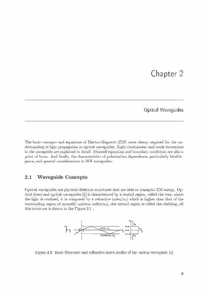
Optical waveguides are physical dielectric structures that are able to transport EM energy. Op-tical �bers and optical waveguides [1] is characterized by a central region, called the core, wherethe light is con�ned, it is composed by a refractive index(n1) which is higher than that of thesurrounding region of normally uniform index(n0), this second region is called the cladding, allthis structure is shown in the Figure 2.1 .
Figure 2.1: Basic Structure and refractive index pro�le of the optical waveguide [1]
5

2.1. Waveguide Concepts
2.1.1 Waveguide Parameters
The propagation characteristics of a waveguide can be expressed in terms of certain parameters,this parameters are explained in the following subsection and shown in Figure 2.1 , which isa typical waveguide cross-section. Also, when necessary, equations to describe and obtain thisparameters will be displayed.
2.1.1.1 Refractive Index
In optics the refractive index [16] , n, of a substance (optical medium) is a number that describeshow light, or any other radiation, propagates through that medium.
Its most elementary occurrence (and historically the �rst one) is in Snell′s law of refraction,n1 sinφ1 = n0 sinφ0, where θ1 and θ0 are the angles of incidence of a ray crossing the interfacebetween two media with refractive indices n1 and n0. Brewster′s angle, the critical angle fortotal internal re�ection, and the re�ectivity of a surface also depend on the refractive index, asdescribed by the Fresnel equations.
2.1.1.2 Birefringence
The birefringence [17] or strength of the double refraction is the property of having two refractiveindices, and the numerical di�erence between the minimum and maximum refractive indices isits quanti�able value (Equation 2.1), this di�erence in refractive indices occurs in the directionsparallel and perpendicular to the direction of orientation, it depends on the polarization andpropagation direction of light. These materials are said to be optically anisotropic, meaning theyhave di�erent properties in di�erent directions. Another de�nition is the measure of the totalmolecular orientation. This e�ect was �rst described by the Danish scientist Rasmus Bartholinin 1669.
4 η = η‖ − η⊥ (2.1)
2.1.1.3 Total Internal Re�ection
Basically, the guiding of the light is a consequence of a total internal re�ection from the interfacebetween the core and the cladding, generated by the fact that the refractive index of the core n1is higher than the index of the cladding. The condition for total internal re�ection is given byEquation 2.2.
n1 sin(π
2− φ) (2.2)
For the Total Internal Re�ection [2] to occur without any major losses, the angle of incident
light must be bigger than the critical angle θc = sin(n2n1
), as shown in the Figure 2.2.
Where n1 is the index of the core and n2 the index of the cladding. Although, in this Figurewe can conclude that after the condition is followed there is no energy loss, but in reality smalllosses exist due to the absorption in the medium and to the re�ections in the surfaces where thelight enters and leaves the medium.
6

2. Optical Waveguides
Figure 2.2: Re�ection and refraction of a parallel beam [2]
2.1.1.4 Relative Refractive-Index Di�erence
Relative Refractive-Index Di�erence is de�ned as a percentage that represents the di�erencebetween n1 and n0. It is de�ned by the Equation 2.3.
4 =n21 − n20
2n21
∼=n1 − n0n1
(2.3)
2.1.1.5 Numerical Aperture
Numerical Aperture [2] is de�ned as the maximum angle of acceptance of a waveguide. Numer-ically we can obtain it by parting from Equation 2.2 of total internal re�ection in Subsection2.1.1.3 , and since the angle φ is related to the incident angle θ by the Equation 2.4.
sin θ = n1 sinφ ≤√n21 − n20 (2.4)
We can obtain an equation that represents the maximum angle of acceptance, resulting theshown in the next Equation.
θ ≤ sin−1√n21 − n20 ≡ θmax (2.5)
It can also be expressed in function of the Relative Refractive-Index Di�erence, as shown:
θmax = NA = n1√
24 (2.6)
7

2.1. Waveguide Concepts
2.1.2 Guided Modes Formation
For the light to propagate through the waveguide the ray must have a speci�c discrete angle,which excites a particular mode, meaning, each discrete angle is associated to a mode [2]. Modescan also be described with the ray picture in the slab waveguide, as shown in Figure 2.3 whereit is possible to observe the phase fronts which are perpendicular to the incident light rays, thewavelength and the wavenumber, a constant representing the average phase variation of the �eldφ, of light in the core are the following Equations.
λ =λ0n1
(2.7)
k = k0n1 (2.8)
Where λ0 is the wavelength in vacuum and k0 =2π
λ0. Therefore, the propagation constants,
which are very important characteristics of the mode, in the lateral direction (x and z) are givenby the next Equations.
β = k0n1 cosφ (2.9)
κ = k0n1 sinφ (2.10)
Figure 2.3: Picture of "modes" propagating along a waveguide [2]
There are various types of modes, in the classi�cation by polarization we can encounter theTransverse Electric (TE) modes, characterized for having no electric �eld in the direction ofpropagation, and the Transverse Magnetic (TM) modes which are lacking the magnetic �eld inthe direction of propagation. We can also have the Transverse Electro-Magnetic (TEM) modesthat don′t have neither electric nor magnetic �elds in the direction of propagation, and �nallythe Hybrid modes, called this way for its non-zero electric and magnetic �elds in the directionof propagation.
2.1.3 Maxwell′s Equations
In a dielectric medium we can express with Maxwell′s Equations [3] in the following form Equa-tions.
8

2. Optical Waveguides
∇× E = −µ∂H∂t
= ik(µ0ε0
)
1
2H (2.11)
∇×H = ε∂E
∂t= −ikn2(µ0
ε0)
1
2E (2.12)
Where µ and ε represent the permeability and permitivity of the medium, respectively. Andcan be related to their respective values in vacuum, µ0[H/m] and ε0[F/m].
ε = ε0n2 (2.13)
µ = µ0 (2.14)
We can establish electric and magnetic �elds in function of the position in the plane transverseto the z-axis, r, considering that it has an angular frequency ω and it propagates in the z directionwith propagation constant β. Obtaining:
e = E(r)ej(ωt−βz) (2.15)
h = H(r)ej(ωt−βz) (2.16)
With Equations 2.11, 2.12, 2.15 and 2.16 we can get in terms of Cartesian Coordinates theequations, which are the bases to waveguide analysis.
∂Ez∂y
+ jβEy = −jωµ0Hx
−jβEx −∂Ez∂x
= −jωµ0Hy
∂Ey∂x− ∂Ex
∂y= −jωµ0Hz
∂Hz
∂y+ jβHy = jωε0n
2Ex
−jβHx −∂Hz
∂x= jωε0n
2Ey
∂Hy
∂x− ∂Hx
∂y= jωε0n
2Ez
(2.17)
9
2.2. Planar Waveguides
2.2 Planar Waveguides
Planar Waveguides citeokamoto2005fundamentals are the basis of waveguide theory used in PICsand in semi-conductor lasers, its mathematical background is �t to be used in the developmentof Two-Dimensional (2D) slab waveguides and for the rectangular waveguide which requires aThree-Dimensional (3D) analysis, this section will explain and analyze the mentioned waveguidesto obtain a full knowledge of optical waveguide theory.
2.2.1 Slab Waveguides
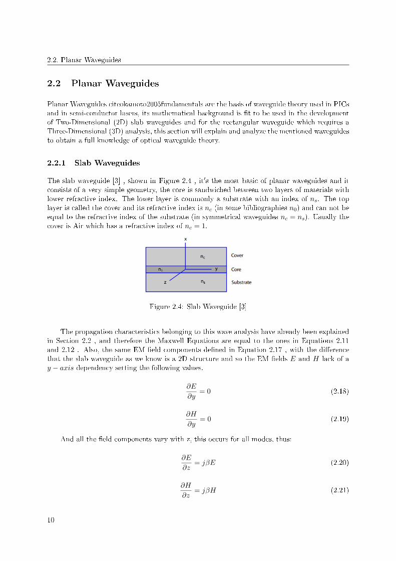
The slab waveguide [3] , shown in Figure 2.4 , it′s the most basic of planar waveguides and itconsists of a very simple geometry, the core is sandwiched between two layers of materials withlower refractive index. The lower layer is commonly a substrate with an index of ns. The toplayer is called the cover and its refractive index is nc (in some bibliographies n0) and can not beequal to the refractive index of the substrate (in symmetrical waveguides nc = ns). Usually thecover is Air which has a refractive index of nc = 1.
Figure 2.4: Slab Waveguide [3]
The propagation characteristics belonging to this wave analysis have already been explainedin Section 2.2 , and therefore the Maxwell Equations are equal to the ones in Equations 2.11and 2.12 . Also, the same EM �eld components de�ned in Equation 2.17 , with the di�erencethat the slab waveguide as we know is a 2D structure and so the EM �elds E and H lack of ay − axis dependency setting the following values.
∂E
∂y= 0 (2.18)
∂H
∂y= 0 (2.19)
And all the �eld components vary with z, this occurs for all modes, thus:
∂E
∂z= jβE (2.20)
∂H
∂z= jβH (2.21)
10

2. Optical Waveguides
These equations produce two di�erent sets of linearly polarized solutions, meaning that weobtain two independent EM modes.
For the TE mode, name which is obtained since the electric �eld lies in the plane that isperpendicular to the z− axis, Ez = 0, Hy = 0 and Ex = 0, and we have the following equationsthat are satis�ed:
d2Eydx2
+ (k20n2 − β2)Ey = 0 (2.22)
wherek0 = ω
√ε0µ0 (2.23)
Hx = − β
ωµ0Ey (2.24)
Hz = − j
ωµ0
dEydx
(2.25)
For TM modes, name given by the fact that the magnetic �eld lies in the plane that isperpendicular to the z − axis, Hz = 0, Hx = 0 and Ey = 0. And are obtained by solving thesame Equation 2.22 written as:
d
dx
(1
n2dHy
dx
)+ (k2 − β2
n2)Hy = 0 (2.26)
where
Ex = − β
ωε0n2Hy (2.27)
Ez = − j
ωε0n2dHy
dx(2.28)
Having the previous equations we can solve separately each layer of the slab waveguide tocalculate the boundary conditions, obtaining:
A cos(κa− φ) exp−σ(x−a) (x > a)
A cos(κx− φ) (−a ≤ x ≤ a)
A cos(κa+ φ) expξ(x+a) (x < −a)
(2.29)
where κ, ξ and σ are wavenumbersin the x− axis in the core and cladding layers. They arede�ned as:
11

2.2. Planar Waveguides
κ2 = k20n
21 − β2
σ2 = β2 − k20n20ξ2 = β2 − k20n2s
(2.30)
At the Hz boundaries the components are continuous, so based on the previous equations:
dEydx
=
−σA cos(κa− φ) exp−σ(x−a) (x > a)
−κA cos(κx− φ) (−a ≤ x ≤ a)
ξA cos(κa+ φ) expξ(x+a) (x < −a)
(2.31)
And the continuity in the boundaries gives:
{σA cos(κa− φ) = κA cos(κx− φ)
κA cos(κx+ φ) = ξA cos(κa+ φ)(2.32)
If we substitute the following we can obtain the eigenvalues mentioned ahead in Equations2.34 and 2.36 :
u = κa
w = ξa
w′ = σa
(2.33)
u =mπ
2+
1
2tan−1
(wu
)+
1
2tan−1
(w′u
)(2.34)
φ =mπ
2+
1
2tan−1
(wu
)− 1
2tan−1
(w′u
)(2.35)
Where m = 0, 1, 2, ...
2.2.2 Rectangular Waveguides
The rectangular waveguide [3] has 3D characteristics and therefore must have another analysis.In these waveguides the light is con�ned in both the x and y dimensions. In the middle corelayer the high index region has a �nite width of 2w and is surrounded on all sides by lower indexmaterials, the refractive index can be di�erent in every side, as shown in Figure 2.5 .
12

2. Optical Waveguides
Figure 2.5: Rectangular Waveguide [3]
Figure 2.6: mode de�nitions and electric �eld distributions in Marcatili′s method [3]
To analyze the best method to follow is the proposed by Marcatili which suggests 2 sim-pli�cations, to ignore the boundary conditions associated with hatched regions and to assumecore-cladding index di�erences are small on all sides. In Figure 2.6 we can see the mode de�ni-tions and the electric �eld distribution (no �elds in the corners of the waveguide).
Taking all these measures into account we can then simply proceed to analyze the rectangularwaveguide as two slab waveguides, one in the y direction and another in the x direction.
First considering EM mode in which Ex and Hy are predominant and setting Hx = 0 we
13

2.2. Planar Waveguides
obtain the wave equation and the EM �eld representation.
∂2Hy
∂x2+∂2Hy
∂y2+ (k20n
2 − β2)Hy = 0 (2.36)
Ex =ωµ0βHy +
1
ωε0n2β
∂2Hy
∂x2
Ey =1
ωε0n2β
∂2Hy
∂x∂y
Ez =−jωε0n2
∂Hy
∂x
Hz =−jβ
∂Hy
∂y
(2.37)
For the other dimension we set Hy = 0 and consider the EM �eld in which Ey and Hx arepredominant we obtain:
∂2Hx
∂x2+∂2Hx
∂y2+ (k20n
2 − β2)Hx = 0 (2.38)
Ex = − 1
ωε0n2β
∂2Hx
∂x∂y
Ey = −ωµ0βHx −
1
ωε0n2β
∂2Hx
∂y2
Ez =j
ωε0n2∂Hx
∂y
Hz =−jβ
∂Hx
∂x
(2.39)
The modes in Equations 2.36 and 2.37 are described as Expq (p and q are integers startingfrom 1). And the modes in Equations 2.38 and 2.39 are described as Eypq . In both cases weobtain the same relations between the transverse wavenumbers kx, ky, γx, and γy.
γ2x = k20(n21 − n20)− k2x (2.40)
γ2y = k20(n21 − n20)− k2y (2.41)
The propagation constant is obtained from
β2 = k20n21 − (k2x + k2y) (2.42)
14

2. Optical Waveguides
If we apply the boundary conditions that the electric �eld Ez is continuous at x = w, andHz in y = d we contain the following dispersion equation:
kxw = (p− 1)π
2+ tan−1
(n21γxn20kx
)(2.43)
kyd = (q − 1)π
2+ tan−1
(γyky
)(2.44)
If we apply the boundary conditions that the magnetic �eld Hz is continuous at x = w, andEz in y = d we contain the following dispersion equation:
kxw = (q − 1)π
2+ tan−1
(γxkx
)(2.45)
kyd = (p− 1)π
2+ tan−1
(n21γyn20ky
)(2.46)
15

Chapter 3
Coupled Mode Theory
The Coupled Mode Theory (CMT) [18] [19] was introduced in 1950′s for microwave devices,it was in the 1970′s when its application extended to optical devices, speci�cally in dielectricwaveguides. The theory is of great use in analyzing devices and predicting fundamental charac-teristics by simple analytic means, and tractable to computational devices. It is essential in theconstruction of practical optical devices dealing with the mutual light-wave interaction betweentwo propagation modes. In the following chapter we will present the derivation of the coupledmode equations, and we will explain the details of important devices.
3.1 Coupled Mode Equations
In this section we will present the EM derivations of the coupled-mode equations [19] partingfrom the con�guration of a basic slab dielectric waveguide. The emntioned waveguide consists ofa �lm of thickness t and index of refraction n2 sandwiched between 2 mediums, the cover withindex n1 and the substrate with n3 .
3.1.1 TE Modes
Taking∂
∂y= 0, this waveguide can support a �nite number of con�ned TE modes with �eld
components Ey, Hx and Hz. The modes not con�ned in the inner layer are not considered. The�eld component Ey of the TE modes obeys the next wave equation:
∇2Ey =n2ic2∂2Ey∂t2
(3.1)
17
3.1. Coupled Mode Equations
Where i = 1, 2, 3 representing the three regions of the waveguide. We take Ey(x, z, t) in theform:
Ey(x, z, t) = Ey(x) expi(ωt−βz) (3.2)
In which the transverse function Ey(x) is equal to:
Ey(x) =
C exp−(qx), 0 ≤ x <∞C[cos(hx)− q
hsin(hx)], −t ≤ x ≤ 0
C[cos(ht) +q
hsin(ht)] expp(x+t), −∞ < x ≤ −t
(3.3)
Which applied to each region we obtain:
h = (n22k2 − β2)1/2
q = (β2 − n21k2)1/2
p = (β2 − n23k2)1/2
k =ω
c
(3.4)
The condition of continuity of components Ey and Hz is that it must be continuous in x = 0and in x = −t and so we get the next equation:
tan(ht) =q + p
h(
1− pq
h2
) (3.5)
Which is used with Equation 3.4 to determine the eigenvalues β of the con�ned TE modes.
If the mode with Ey = AEy(x) which corresponds to a power �ow of |A|2W/m wants to benormalized we determine C with the next condition:
− 1
2
∫ ∞−∞
EyH∗x dx =
βm2ωµ
∫ ∞−∞
[E(m)y (x)]2 dx = 1 (3.6)
Cm = 2hm
ωµ
|Bm|(t+
1
qm+
1
pm
)(h2m + q2m)
1
2
(3.7)
Since the Ey are orthogonal we obtain:∫ ∞−∞E(l)y E(m)
y dx =2ωµ
βmδl,m (3.8)
18

3. Coupled Mode Theory
3.1.2 TM Modes
Taking∂
∂y= 0, this waveguide can support a �nite number of con�ned TM modes with �eld
components Hy, Ex and Ez. The modes not con�ned in the inner layer are not considered. The�eld components of the TM modes are:
Hy(x, z, t) = Hy(x) expi(ωt−iβz)
Ex(x, z, t) =i
ωε
∂Hy
∂z=
β
ωεHy(x) expi(ωt−βz)
Ez(x, z, t) = − i
ωε
∂Hy
∂x
(3.9)
The transverse function Hy(x) is:
Hy(x) =
−C
[h
qcos(ht) + sin(ht)
]expp(x+t), x < −t
C
[−hq
cos(hx) + sin(hx)
], −t < x < 0
−hqC exp−qx), x > 0
(3.10)
The continuity of Hy and Ez requires that the propagation constants obey the eigenvalueequation:
tan(ht) =h(p+ q)
h2 − pq(3.11)
Where
p =n22n23p
q =n22n21q
(3.12)
To normalize the constant so that the �eld carries 1 W per unit width in the y direction wemust follow the next condition:
1
2
∫ ∞−∞
HyE∗x dx =
β
2ω
∫ ∞−∞
H2y(x)
εdx = 1 (3.13)
19

3.1. Coupled Mode Equations
where n21 = ε1/ε0 so we obtain:
Cm = 2
√ωε0
βmteff
teff =q2 + h2
q2
[1
n22+q2 + h2
q2 + h21
n21q+p2 + h2
p2 + h21
n23p
] (3.14)
3.1.3 The Coupling Equation
The wave equation obeyed by the unperturbed modes is:
∇2E(r, t) = µε∂2E
∂t2(3.15)
We can represent the perturbation as a distributed polarization source Ppert(r, t), whichaccounts for the deviation of the medium polarization from that which accompanies the un-perturbed mode. The wave equation for the perturbed case follows directly from Maxwell′sequations if we take D = ε0E + P.
∇2Ey(r, t) = µε∂2Ey∂t2
+ µ∂2
∂t2[Ppert(r, t)]y (3.16)
Similar equations correspond to the remaining components in the other directions.
If we take the eigenmodes of Equation 3.15 as an orthonormal set, and we assume slowvariation so that d2Am/dz
2 << βm dAm/dz, and recalling that E(m)y (x) expi(ωt−βmz) obeys the
unperturbed Equation 3.15 we obtain:
∑l
[−iβl
dAldz
E(l)y (x) expi(ωt−βlz)
]+ c.c. = µ
∂2
∂t2(Ppert)y (3.17)
Where l extends over the discrete set of con�ned modes and includes both positive andnegative traveling waves.
Multiplying Equation 3.17 with E(m)y (x), integrating and making the orthogonality relation
mention before we �nally attain the following equation:
dA(−)m
dzexpi(ωt+βmz)−dA
(+)m
dzexpi(ωt−βmz) +c.c. =
−i2ω
∂2
∂t2
∫ ∞−∞
[Ppert(r, t)]y E(m)y (x) dx (3.18)
Where A(−)m is the complex mode amplitude of the negative traveling TE mode while A(+)
m
is the positive traveling TE mode.
20

Chapter 4
MMI Self-Imaging Model
The operation of any optical MMI device is based on the self-imaging principle [4] of periodicobjects illuminated by coherent light, this principle was �rst described as a property of multimodewaveguides by which an input �eld pro�le is reproduced in single or multiple images at periodicintervals along the propagation direction of the guide.
4.1 MultiMode Waveguides
The main structure of the MMI device is a multimode waveguide [4], which has the property ofbeing able to propagate more than 3 modes. To excite these modes it is necessary to incorpo-rate to the mentioned structure the input and output segments or waveguides which in will besinglemode.
For an analytic point of view a full Modal Propagation Analysis (MPA) is of great use sincethe �eld distribution of the waveguide modes can be determined. To be allowed to easily optimizethe device structure it is of essential use the BPM method.
4.1.1 Propagation Constants
The multimode waveguide is composed by a ridge of an e�ective refractive index of nr of widthWM and a cladding with a e�ective refractive index of nc as shown in Figure 4.1 .
The waveguide is able to propagate m lateral modes with modes numbers v = 0, 1, ...(m−1)as shown in Figure 4.2
The propagation constant βv and the lateral wavenumber kyv are related to the ridge indexby the dispersion equation:
21

4.1. MultiMode Waveguides
Figure 4.1: 2D representation of the refractive step index pro�le and top view of the multimodewaveguide [4]
Figure 4.2: Amplitude-normalized lateral �eld pro�les [4]
kyv2 + β2v = k20n
2r (4.1)
where
k0 =2π
λ0
kyv =(v + 1)π
Wev
(4.2)
Where the e�ective widthWev takes into account the polarization dependent lateral penetra-tion depth of each mode �eld, associated with the Goos-Hähnchen shift at the ridge boundaries.In general the e�ective widths Wev can be approximated by the e�ective width We0 correspond-ing to the fundamental mode.
Wev 'We = WM +
(λ0π
)(ncnr
)2σ
(n2r − n2c)−1/2 (4.3)
22

4. MMI Self-Imaging Model
Where σ = 0 for TE and σ = 1 for TM polarization. By using binomial expansion withkyv
2 � k20n2r , the propagation constant can be deduced into:
βv ' k0nr −(v + 1)2πλ0
4nrW 2e
(4.4)
Therefore, the propagation constants in a step-index multimode waveguide show a nearlyquadratic dependence with respect to the mode number v. By de�ning Lπ as the beat length ofthe two lowest order modes:
Lπ =π
β0 − β1' 4nrW
2e
3λ0(4.5)
And the propagation constants spacing can be expressed as:
(β0 − β1) 'v(v + 2)π
3Lπ(4.6)
4.1.2 Guided Mode Propagation Analysis
An input pro�le Ψ(y, 0) imposed at z = 0 and totally contained within We will be decomposedinto the modal �eld distributions ψv(y) of all modes as shown in Figure 4.3 .
Figure 4.3: Input �eld and mirrored images in the multimode waveguide [4]
Ψ(y, 0) =∑v
cvψv(y) (4.7)
Where the summation should be understood as including guided as well as radiative modes.The �eld excitation coe�cients cv can be estimated by using overlap integrals:
cv =
∫Ψ(y, 0)ψv(y) dy√∫
ψ2v(y)dy
(4.8)
23

4.2. General Interference
If the spatial spectrum of the input �eld is narrow enough to avoid the excitation of unguidedmodes, it can be decomposed into guided modes alone.
Ψ(y, 0) =
m−1∑v=0
cvψv(y) (4.9)
From which we can determine the �eld at a distance z that can be written as a superpositionof all the guided mode �eld distributions:
Ψ(y, 0) =
m−1∑v=0
cvψv(y) expj(ωt−βvz) (4.10)
Or
Ψ(y, 0) =
m−1∑v=0
cvψv(y) expj(β0−β1)z (4.11)
Therefore, substituting Equation 4.6 we obtain the expression with distance z = L.
Ψ(y, 0) =
m−1∑v=0
cvψv(y) exp
[j(v(v + 2)π
3Lπ)L
](4.12)
The di�erent images formed will be determined by the modal excitation cv, and the propertiesof the mode phase factor.
exp
[jv(v + 2)π
3LπL
](4.13)
4.2 General Interference
Self-Imaging interference mechanism in which the images are independent of the modal excita-tion, in this category we have the formation of both the single and the multiple images.
4.2.1 Single Images
The single images are those that are a replica of the input �eld, meaning the single image obtainedat Ψ(y, L) will be equal to the image of Ψ(y, 0), if:
exp
[jv(v + 2)π
3LπL
]= 1 or (−1)v (4.14)
24

4. MMI Self-Imaging Model
The �rst condition refers to the phase changes of all the modes along L and that it mustdi�er by integer multiples of 2π. The replica of the input occurs due to the fact that all theguided modes interfere with the same relative phases, these images are called also direct image.
The second condition means that the phase changes must alternate between odd and evenmultiples of π. This produces the existence of even modes that will be in phase with the inputand the odd modes which will be the anti-phase of the same.
Due to the odd symmetry the interference produces a mirrored image with respect to they = 0 plane. We can see this characteristic in the following Equation:
ψv(−y) =
{ψv(y) for v even
−ψv(y) for v odd(4.15)
and in
v(v + 2) =
{even for v even
odd for v odd(4.16)
Following the property shown in Equation 4.16 and taking into account the conditions inEquation 4.14 we can deduce that it will be ful�lled at:
L = p(3Lπ) with p = 0, 1, 2, ... (4.17)
Where p denotes the periodic nature of the imaging through the multimode waveguide.Therefore, the direct and mirrored single images of the input �eld Ψv(y, 0) will be formed bygeneral interference at a z distance which are, respectively, even and odd multiples of the length(3Lπ).
4.2.2 Multiple Images
Multiple images are also obtained as a result of the input �eld in Ψv(y, 0), these are obtainedbetween the single images determined to be ful�lled at distances given by Equation 4.17 .
If we consider uniquely the images positioned half-way between the direct and the mirroredimages, meaning the following positions:
L =p
2(3Lπ) with p = 1, 3, 5, ... (4.18)
In which we can �nd the �elds by substituting the length into the �eld pro�le,
25
4.2. General Interference
Ψ(y,p
23Lπ) =
m−1∑v=0
cvψv(y) exp[jv((v + 2)p(
π
2)]
(4.19)
Where p is an odd integer, and where if applied the conditions and properties of symmetrywe obtain:
Ψ(y,p
23Lπ) =
∑v even
cvψv(y) +∑v odd
(−j)pcvψv(y)
=1 + (−j)p
2Ψ(y, 0) +
1− (−j)p
2Ψ(−y, 0)
(4.20)
These pair of images obtained from the input �eld are in quadrature and have an amplitudeof 1/
√2, also they are separated between each other by a distance in the propagation direction
of z =1
2(3Lπ),
3
2(3Lπ), ... . This is essential and can be used to produce the 2x2 3-dB coupler.
As seen, the multi-fold images are formed at intermediate z positions. The positions and thephases of the N-fold images at a certain z distance is calculated by using Fourier analysis andproperties of generalized Gaussian sums. To perform this analysis we introduce a �eld Ψin(y) asan extension of the input �eld, asymmetric respect to the y = 0 plane and with periodicity of2We .
Ψin(y) =∞∑
v=−∞[Ψ(y − v2We, 0)−Ψ(−y + v2We, 0)] (4.21)
We can approximate the mode �eld amplitudes to a sine-like function
ψv(y) ' sin(kyvy) (4.22)
Permitting to considerate it as an Fourier expansion at distances
L =p
N(3Lπ) (4.23)
Where p ≥ 0 and N ≥ 1 are integers with no common divisors, and the �eld will be expressedas follows:
Ψ(y, L) =1
C
N−1∑q=0
Ψin(y − yq) exp(jϕq) (4.24)
where
26

4. MMI Self-Imaging Model
yq = p(2q −N)We
N(4.25)
ϕq = p(N − q)qπN
(4.26)
And C is a complex normalized constant with |C| =√N , p refers to the imaging periodicity
along the direction of z , and q represents each of the N images along the y direction.
The mentioned equations show that, at distances z = L, N images are formed of the extended�eld Ψin(y) located at the position yq , each with amplitude 1/
√N and phase ϕq. This leads
to N images, generally not equally spaced between them, of the input �eld, being formed insidethe physical guide and within the lateral boundaries.
The multiple self-imaging mechanism allows the realization of NxN or NxM optical couplers.Shorter devices are obtained with p = 1. Optical phases for the NxN case is given by thefollowing:
ϕrs =π
4N(s− 1)(2N + r − s) + π for r + s even (4.27)
ϕrs =π
4N(r + s− 1)(2N − r − s+ 1) + π for r + s odd (4.28)
where r = 1, 2, ...N is the numbering of the input waveguides (bottom-up) and s = 1, 2, ...Nis the numbering of the output waveguides (top-down).
4.3 Restricted Interference
MMI Couplers permit the restriction of the modal excitation [4], meaning, it is possible to excite,by the input �elds, only some of the guided modes in the multimode waveguide. This selectiveexcitation reveals interesting multiplicities of v(v + 2) which allow new interference mechanismsthrough shorter periodicities of the mode phase factor.
4.3.1 Paired Interference
The selective excitation of modes can o�er us certain advantages, like for example when:
mod3[v(v + 2)] = 0 for v 6= 2, 5, 8, ... (4.29)
We reduce the length periodicity of the mode phase factor 3 times the original size, but alsothe following condition must be taken into account.
27

4.3. Restricted Interference
cv = 0 for v = 2, 5, 8 (4.30)
Resulting in lengths of direct and inverted images, of the input �eld, determined by the nextequation:
L = p(Lπ) with p = 0, 1, 2, ... (4.31)
As long as the mentioned modes are not excited in the multimode waveguide. Parting fromthis point we can determine the length of N-fold images:
L =p
N(Lπ) (4.32)
where p ≥ 0 and N ≥ 1 are integer with no common divisors.
Now that we have explained the advantage, the procedure to excite the wished modes isdetailed. To obtain this behavior we must launch an even symmetric input �eld Ψ(y, 0), usuallya Gaussian beam, at y = ±We/6. Position where the modes v = 2, 5, 8, ... present a zero withodd symmetry. The overlap of the integrals of the �eld excitation coe�cient cv between thesymmetric input and the asymmetric mode �elds will vanish and therefore we will obtain cv = 0for v = 2, 5, 8, ..., in this case the input waveguides are limited to 2.
When the selective excitation is performed, the modes contributing to the imaging will bepaired, the mode pairs 0-1, 3-4, 6-7 and so on, which will have similar properties, based on thisfact they obtain the name paired interference.
A very used case of this restricted interference is the 2x2 MMI Coupler or the Two ModeInterference (TMI), commonly used in silica based dielectric rib type waveguides.
4.3.2 Symmetric Interference
This selective excitation of a 1-to-N beam splitter in which the modes excited are the evensymmetrical can produce the shortage of four times the original result of the waveguides length.As in the previous restricted interference we will proceed to explain through an example, where:
mod4[v(v + 2)] = 0 for v even (4.33)
Having a reduction of the length periodicity of the mode phase when the following conditionis ful�lled:
cv = 0 for v = 1, 3, 5, ... (4.34)
Consequently the direct and inverted single images of the input �eld Ψ(y, 0) will be obtainedat the length of:
28

4. MMI Self-Imaging Model
L =p
N
(3Lπ
4
)(4.35)
With N images of the input �eld, symmetrically located along the y-axis with equal spacingWe/N .
In the symmetrically excited MMI Couplers at half the self imaging length we can observethe formation of the 2-fold image, and as the length diminishes the number of images increasesaccordingly to the Equation 4.35 , until they are no longer resolvable.
We can generalize that to obtain a low-loss well-balanced 1-to-N splitting of a Gaussianbeam the multimode waveguide must support at least m = N + 1 modes. The most commonand simple of symmetric interference is the 1x2 MMI coupler, needing only 2 symmetric modes.
29

Chapter 5
Fabrication Techniques
Throughout this chapter the process of fabrication of a Silicon Waveguide Devices [5] will be ex-plained in detail, passing through the diversity of choices in methods to obtain the characteristicsof the mentioned devices. The usage of this material in the fabrication of photonic devices is dueto the low primary cost of the material, the mature and well characterized processing techniquesthat have been highly researched, developed and manufactured in the microelectronic industrywhich present an enormous advantage and permits the future fusion of both industries.
5.1 Silicon-on-Insulator (SOI)
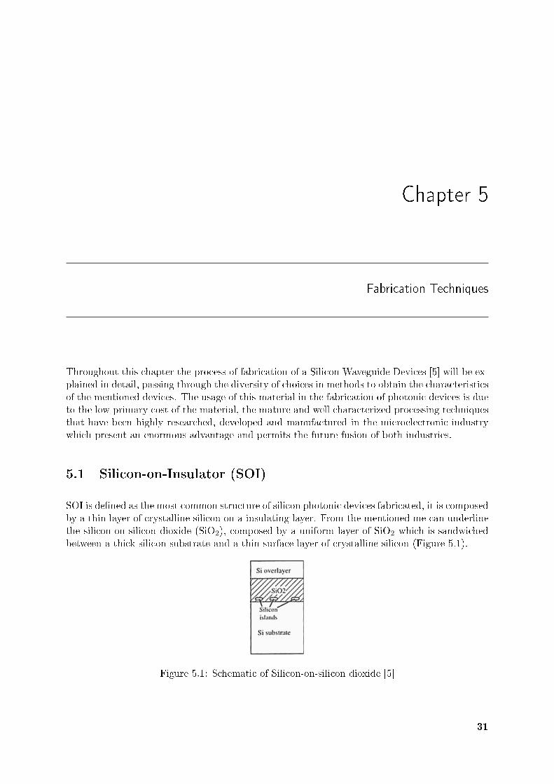
SOI is de�ned as the most common structure of silicon photonic devices fabricated, it is composedby a thin layer of crystalline silicon on a insulating layer. From the mentioned me can underlinethe silicon-on-silicon dioxide (SiO2), composed by a uniform layer of SiO2 which is sandwichedbetween a thick silicon substrate and a thin surface layer of crystalline silicon (Figure 5.1).
Figure 5.1: Schematic of Silicon-on-silicon dioxide [5]
31

5.1. Silicon-on-Insulator (SOI)
The SiO2 has a refractive index of 1.46, and the crystalline silicon layer of 3.5, considerablyhigher and there for generating a speci�c type of SOI forming a classic waveguide form. Bothlayers of crystalline silicon and the buried silicon dioxide layer are characterized by having athickness in the order of microns, but its value can change depending of the method of fabrication.The most commonly used are the explained in the following subsections.
5.1.1 Separation by IMplanted OXygen (SIMOX)
The SIMOX [5] consists on the implantation of a large amount of oxygen ions below the surfaceof a silicon wafer (Figure 5.2). Its simplicity is a factor of relevance that quali�es it as the mostcommon method for the fabrication of large volumes of SOI material.
To describe the total amount of any ion species implanted into a wafer the implanted iondose is used. The ion dose is the total number of ion that pass through one square centimeter ofthe wafer surface, this is measured in units of ions/cm2.
In the SIMOX process it is required to present a total implantation dose of over 1018cm−2,and under normal temperatures we will obtain unwanted amorphous silicon over-layers, thereforeit must be kept at a temperature of 600◦C during the implantation on the silicon substrate.
In this process we obtain a certain depth of the SiO2, and hence the thickness of the siliconoverlayer, through the energy used to implant the oxygen ions into the crystalline silicon. Thementioned energy can go up to 200keV , and the consequences in depth from oxygen variationare viewed in the pro�les showed in Figure 5.3 .
Where we can observe certain behaviors, in the case where we have the application of lessthan 1016cm−2 we get as a pro�le a gaussian function. As the oxygen dose increases, the peakconcentration of ions (O+) saturates to a concentration of that found in stoichiometric SiO2,with further implantation over 1018cm−2, the oxygen pro�le begins to �atten forming a buriedand continuous layer of SiO2. and �nally the silicon wafer is annealed at a temperature of 1300◦C for several hours, this produces a uniform buried SiO2 layer with distinct interfaces with 2adjacent silicon layers. The annealing insures the silicon overlayer is denuded of implantationrelated, primary lattice defects.
The concentration of secondary defects in the silicon overlayer is of great importance to siliconphotonics, and the micro-roughness of the silicon overlayer surface and the overlayer/buried oxideinterface.
5.1.2 Bond and Etch-back SOI (BESOI)
This process is the result of the use of a phenomenon produced by the intimate contact of twohydrophilic surfaces [5], such as SiO2, that creates a highly strong bond between them. Theprocess follows three steps which are shown in Figure 5.4 .
The steps are following:
(a) Oxidation of 2 wafers to be bonded.
32

5. Fabrication Techniques
Figure 5.2: SIMOX processing schematic [6]
(b) Formation of the chemical bond.
(c) Thinning (etching) of one of the wafers.
The bonding process is done by bringing the wafers into contact at room temperature, wherethe initial bond is formed. The bond strength is increased to that of bulk material via subsequentthermal processing to temperatures as high as 1100 ◦C.
The etching or wafer thinning uses the Chemical Mechanical Polishing (CMP) technique,commonly used in microelectronics for wafer planarization. CMP requires that the wafer surfacebe both weakened and subsequently removed during a single processing step.
33

5.1. Silicon-on-Insulator (SOI)
Figure 5.3: Variation of oxygen pro�le during the SIMOX process [5]
Figure 5.4: BESOI process [5]
• The silicon surface to be polished is brought into contact with a rotating pad, and simul-taneously a chemically reactive slurry containing an abrasive component, such as aluminaand glycerin, weakens and removes surface layers.
• The process removes the majority of the polished bonded wafer, leaving a thin siliconoverlayer on a buried SiO2 layer, supported by a silicon substrate.
• The removing method limits the achievable thickness for the silicon overlayer to around 10microns.
An improvement in SOI thickness uniformity can be achieved by the use of an End-Stop inthe thinning process reducing or even eliminating the need for CMP. This improvement is basedon the application of the following modi�cation.
1. Subsequently from the creation of the heavily doped p-type layer, a further, undopedintrinsic layer is epitaxially grown on the wafer surface.
2. Afterwards, a second non-selective etched process is used to remove the exposed p-typelayer following the selective etch.
3. The �nal wafer is then a structure of one undoped silicon overlayer on the buried SiO2.
34

5. Fabrication Techniques
5.1.3 Wafer Splitting (SmartCut Process to produce Unibond Wafers)
It is considered to be the fusion of the SIMOX and the BESOI [6] [5]. The steps that describethe process are shown in Figure 5.5 .
Figure 5.5: Smart Cut process [5]
(a) Thermally oxidized wafer is implanted with a high dose of hydrogen, approximately 1017cm−2.The implanted hydrogen ions form a gaussian-like pro�le. The distance from the wafer sur-face of the peak of the pro�le depends on the H+ ion energy, usually between a few hundrednanometers and a few microns. The hydrogen ions, and the silicon lattice damage causedby the stopping of the ions, are at their greatest concentration at this depth, and here thesilicon lattice bonds are signi�cantly weakened.
(b) A second wafer (which mayor may not have a thermal SiO2-covered surface) is bonded tothe �rst as in the BESOI process.
(c) The thermal processing at 600 ◦C and 1100 ◦C splits the implanted wafer at a point consistentwith the range of hydrogen ions. A�ne CMP is employed (Figure 5.6) to reduce roughnessat the SOI surface.
To increase the thickness of the silicon overlayer can be obtained by the use of the epitaxialsilicon growth. The non-uniformity of the position of the implanted hydrogen pro�le peak andtherefore the overlayer thickness are only a few percent. Although the overlayer receives a highdose implant, the small mass of the hydrogen ion ensures that negligible residual damage remainsat the end of the thermal processing.
5.1.4 Silicon Epitaxial Growth
Epitaxial means that the grown layer is a ordered mono-crystal [5], essential if e�cient opto-electrical devices are to be fabricated.
The use of epitaxial silicon as the waveguiding medium has the additional advantage ofdoping and defect levels bellow those found in wafers cut from an ingot following bulk growthusing the Czochalski (Cz) or Floating Zone (FZ) methods.
35

5.1. Silicon-on-Insulator (SOI)
Figure 5.6: Smart Cut detailed process (sub-steps)[6]
The most common epitaxial silicon growth technique is Chemical Vapor Deposition (CVD),process which deposits a solid �lm on the surface of a silicon wafer by the reaction of a gas mixturea that surface. For silicon deposition, dichlorosilane (SiH2Cl2) is often used as the source gas.
The wafer surface must be raised in temperature (over 1000◦C) to create the chemical re-action. The desired thickness of the �lm required in silicon waveguide fabrication dictates theuse of vapor phase epitaxy, although a solid source can also be used with Molecular Beam Epi-
36
5. Fabrication Techniques
taxy (MBE). The resulting non-uniformity by this process is less than 1%.
5.2 Fabrication of Surface Etched Features
To this point the fabrication of SOI material, structures that are used in the guidance of thelight, but in this section we will approach features that provide lateral con�nement to the men-tioned structures, characteristic of great importance will designing the slab the waveguide. Thefabrication steps in forming the rib and other guiding structures in the silicon overlayer will beexplained in this section.
5.2.1 Photolithography
The control of the photo process is one of the most important factors in silicon photonic fabrica-tion since the width of the rib waveguide is determined by its photolithographical characteristics.
To control the dimensions and obtain a minimal feature size at a level of 10nm the CriticalDimension (CD) is used, this control is in excess of that required to form the most basic of siliconphotonic structures such as large-cross-section and the singlemode silicon rib.
5.2.1.1 Wafer Preparation
This process is basically the elimination of contaminate particles on the surface of the wafer, andlater on it must be desorbed of any moisture. The latest is a great necessity since the cleaningprocess is done via a wet process, ending in a DI wafer rinse and dry, to achieve this the wafer isbaked at 150 ◦C , then the wafer is coated with an adhesion promoter (hexamethyldisilazane).
5.2.1.2 Photoresist Application
To create a better control when fabricating exotic devices or waveguides with dimensions whichare submicron photolithography transfers a mask-de�ned pattern to the wafer by printing on itssurface using a photosensitive polymer called photoresist.
The application is performed by �rst coating the wafer with liquid photoresist followingpreparation. The resist is dispensed on the center of the wafer which is held via a vacuum sealon a metal or polymer chuck. When approximately 10 ml of this liquid has been dispensed, thewafer is spun at a typical speed of 1-5 krmp, this distributes the resist over the entire surface ofthe wafer (Figure 5.7).
5.2.1.3 Soft Bake
A post-spin soft bake is used to drive o� most of the solvents in the resist while at the same timeimproving resist uniformity and adhesion, this is performed at 100 ◦C for a few minutes.
37

5.2. Fabrication of Surface Etched Features
Figure 5.7: The SOI wafer is uniformly coated with a thin polymer known as photoresist [5]
5.2.1.4 Exposure to Ultraviolet Light
The wafer is transferred to the mask-aligner where it is placed, with sub-micron precision, relativeto the permanent pattern de�ned on the mask. Unless this is the �rst wafer layer, the patternwill be integrated with all previous layers. Once correctly aligned, the wafer is exposed to UVlight (Figure 5.8).
Figure 5.8: The resist is exposed to UV light through a permanent mask. The mask shown hereis designed to result in waveguide formation [5]
When the process performed is Positive Resist the light passes through the transparentregions of the mask and activates the photosensitive components of the resist, such that theseareas of resist are removed during the developing stage as shown in Figure 5.9 .
In the Negative Resist process the unexposed areas are removed.
5.2.1.5 Photoresist Developing
At this stage the pattern is created, where the wafer is exposed to a developing solution. Whetherthe process is positive or negative resist, the solution will dissolve the activated resist, or theun-activated, leaving the resist pattern intact.
5.2.1.6 Hard Bake
This process drives o� the remaining resist solvents and further strengthens the resist adhesionto the wafer surface. It is typically performed at a temperature of 90-140 ◦C for several minutes,
38

5. Fabrication Techniques
Figure 5.9: Dry etching using positive photoresist during a photolithography process [7]
the upper limit of the mentioned temperatures must be such that the hardbake does not resultin pattern deformation via resist �ow. Following hardbake, the desired pattern is printed in thephotoresist (Figure 5.10).
39

5.2. Fabrication of Surface Etched Features
Figure 5.10: Following hardbake, the desired pattern is printed in the photoresist ready fortransfer to the wafer [5]
5.2.2 Silicon Etching
Silicon Etching is divided in two categories, Wet Etching and Dry Etching, both have great ad-vantages and disadvantages, but to reproduce features of submicron dimensions the Dry Etchingapproach is the best option. The wet etching employs a liquid chemical agent to remove theuppermost layer of the substrate in the areas that are not protected by the photoresist, the dryetching performs the same procedure but by the use of a plasma chemical agent instead.
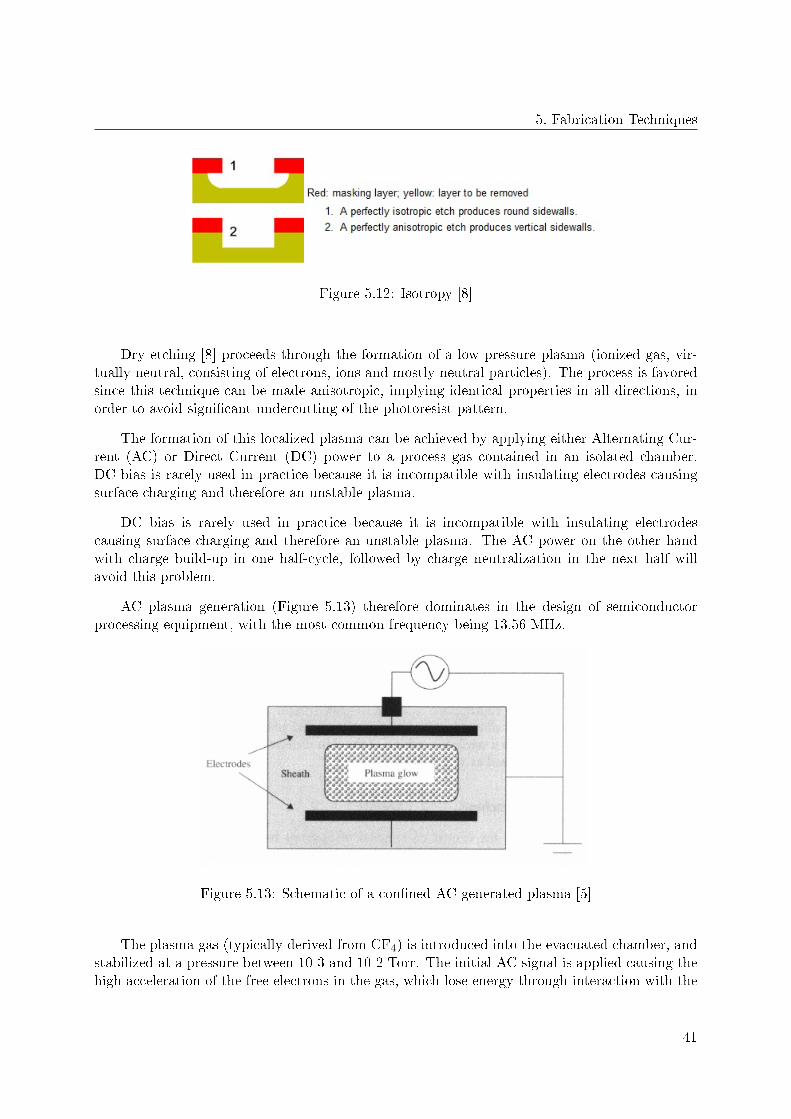
When etching two characteristics [8] are of great importance, Selectivity (Figure 5.11) andIsotropy (Figure 5.12).
Selectivity If the etch is intended to make a cavity in a material, the depth of the cavitymay be controlled approximately using the etching time and the known etch rate. Moreoften, though, etching must entirely remove the top layer of a multilayer structure, withoutdamaging the underlying or masking layers. The etching system's ability to do this dependson the ratio of etch rates in the two materials.
Figure 5.11: Selectivity [8]
Isotropy Some etches undercut the masking layer and form cavities with sloping sidewalls.The distance of undercutting is called bias. Etchants with large bias are called isotropic,because they erode the substrate equally in all directions. Modern processes greatly preferanisotropic etches, because they produce sharp, well-controlled features.
Low-loss waveguides have been produced in both approaches, having small dimensions (typ-ically > 1µm), and having characteristics like �exible process capability, tight tolerances andreproducible production.
40
5. Fabrication Techniques
Figure 5.12: Isotropy [8]
Dry etching [8] proceeds through the formation of a low pressure plasma (ionized gas, vir-tually neutral, consisting of electrons, ions and mostly neutral particles). The process is favoredsince this technique can be made anisotropic, implying identical properties in all directions, inorder to avoid signi�cant undercutting of the photoresist pattern.
The formation of this localized plasma can be achieved by applying either Alternating Cur-rent (AC) or Direct Current (DC) power to a process gas contained in an isolated chamber.DC bias is rarely used in practice because it is incompatible with insulating electrodes causingsurface charging and therefore an unstable plasma.
DC bias is rarely used in practice because it is incompatible with insulating electrodescausing surface charging and therefore an unstable plasma. The AC power on the other handwith charge build-up in one half-cycle, followed by charge neutralization in the next half willavoid this problem.
AC plasma generation (Figure 5.13) therefore dominates in the design of semiconductorprocessing equipment, with the most common frequency being 13.56 MHz.
Figure 5.13: Schematic of a con�ned AC generated plasma [5]
The plasma gas (typically derived from CF4) is introduced into the evacuated chamber, andstabilized at a pressure between 10-3 and 10-2 Torr. The initial AC signal is applied causing thehigh acceleration of the free electrons in the gas, which lose energy through interaction with the
41

5.2. Fabrication of Surface Etched Features
gas atoms via processes such as molecular ionization and dissociation. The excited gas in turngives rise to the emission of light and a distinctive glow is observed. The color of the glow isdependent on the elemental constituents of the gas.
The vast disparity between the mass of the electrons and ions results in a time-averagedbuild-up of negative charge at the electrode surfaces, and a subsequent depletion of electrons inthe gas volume close to the electrodes. Without electrons to drive the process, the excitation ofthe plasma gas in these volumes ceases and dark regions form (this is commonly referred to as asheath).
The result (Figure 5.14) is an e�ective plasma potential (Vp), greater than the potential ateither electrode, causing the acceleration of positively charged ions to the grounded electrode onwhich the process wafer is usually placed.
Figure 5.14: Time-averaged potential distribution in the plasma chamber [5]
Another technique used is the Reactive Ion Etch (RIE) which uses both chemical (reactive)and physical (sputtering) processes to remove material from the wafer surface. Unlike the genericetch chamber described above, the wafer is positioned on the AC driven electrode, which issigni�cantly smaller than the grounded electrode. This way, a large voltage develops between theplasma and the wafer, ensuring the plasma-generated reactive ions have a degree of directionalitynormal to the wafer surface.
This in turn ensures preferential etching in the direction of acceleration. An importantconsideration in any silicon etching process (both wet and dry), but particularly for RIE, is theneed for selectivity to the masking material. In general the greater the degree of physical etchingused, the greater the erosion of the masking medium (usually photoresist).
5.2.3 Critical Dimension Control
A CD [9] is one or more features de�ned by the circuit designer or wafer process engineer asbeing the most important with respect to dimensional control. The features may be oriented inthe X and Y direction and may be clear or opaque. The 3 parameters that are important are:
42

5. Fabrication Techniques
1. The average value of a given critical dimension relative to the specialized value.
2. The uniformity of the critical dimension.
3. The linearity of feature sizes down to some lower limit.
The accuracy of the linewidth measuring tool and the cross-section pro�le of the featuresplay an important role in determining the mentioned parameters, each of which has a uniquee�ect on the wafer processing, as described ahead.
The correct average measure size (Parameter 1) is important to maintain the wafer exposurelevel that gives maximum exposure latitude. Biasing the wafer exposure to compensate fora large deviation in the average mask CD reduces the available exposure latitude. Also, largevariations from one mask level to another requires re-calibrating the wafer exposure level. The CDuniformity (Parameter 2) is important to yield maximum circuit performance. The importanceof feature size linearity (Parameter 3) is dependent on the circuit design.
All of the steps in forming a silicon rib will e�ect a change in the dimensions of the rib, andeach requires characterization and constant monitoring. In high-volume manufacture this willentail the use of Statistical Process Control (SPC).
The dimensions critical to waveguide performace are described in Figure 5.15 .
Figure 5.15: Schematic of a silicon waveguide. The dimensions critical to device performance arehighlighted: rib width (W ), silicon overlayer thickness (h), silicon thickness following rib etch(r) and rib wall angle (θ) [9]
The silicon overlayer thickness (h) is determined primarily by the process used to produce theSOI waveguiding layer. Silicon-on-SiO2 lends itself particularly well to optical characterization,such as that performed with an infrared re�ectometer or ellipsometer, and hence material maybe screened easily prior to the fabrication of silicon photonic circuitry.
The width of the rib (W) and the rib wall angle (θ) depend on both the photolithographyand the silicon etch. In the case of W , a process bias will exist at each process step. For
43
5.3. MMI Device Fabrication and Innovative Fabrication Techniques
instance, the width of the rib image on the photo hard mask is generally di�erent from thatproduced in the developed photoresist, and the ultimate width of the etched rib will be smallerthan the photoresist image. The rib height (h− r) is determined by the dry silicon etch. Opticalabsorption and interferometric techniques exist allowing the determination of etch depth witha considerable degree of accuracy so-called end-point detection. Subsequent to etch a usefulmethod for measuring an etch depth of micron dimensions is via surface pro�lometry.
Finally, an important consideration in calculating process bias for waveguides which havean upper oxide cladding is the reduction in h, r and W following thermal oxidation. Becausethermal oxidation proceeds via a reaction of oxygen and silicon atoms, the e�ect is a consumptionof silicon and hence reduction of critical dimensions. A comparison of the atomic density of silicon(5x1022cm−3) and the molecular density of SiO2 (2.2x1022cm−3) leads immediately to the factthat, for the growth of a given thickness t of SiO2, a thickness of silicon equal to (0.44t) isconsumed.
5.3 MMI Device Fabrication and Innovative Fabrication Tech-niques
MMI devices, which are based on the structure of a multimode waveguide, are commonly ob-tained through the use of fabrication techniques with great precision such as the SIMOX methodexplained in Section 5.1.1, and surface etched features such as Photolithography and Dry Etchingdetailed in Sections 5.2.1 and 5.2.2. But the increasing scalability of this components have drivenus to the use of more innovative techniques that will o�er as result a high accurate structure atthe nanometer level. In the following sections this techniques will be explained.
5.3.1 Electron-beam Lithography
Electron beam lithography [10], also called e-beam lithography, is the practice of emitting abeam of electrons (Figure 5.16) in a patterned fashion across a surface covered with a �lmcalled the resist,exposing the resist and through selectively removing either exposed or unexposedregions of the resist, this procedure is referred to as the developing stage. The purpose, aswith photolithography, is to create very small structures in the resist that can subsequently betransferred to the substrate material, often by etching. Thanks to this feature we obtain thecreation nanotechnology architectures (Figure 5.17).
The primary advantage of electron beam lithography is that it is one of the ways to beatthe di�raction limit of light and make features in the nanometer regime. This form of masklesslithography has found wide usage in photomask-making used in photolithography, low-volumeproduction of semiconductor components, and research and development.
The key limitation of electron beam lithography is throughput, the very long time it takes toexpose an entire silicon wafer or glass substrate. A long exposure time leaves the user vulnerableto beam drift or instability which may occur during the exposure. Also, the turn-around timefor reworking or re-design is lengthened unnecessarily if the pattern is not being changed thesecond time.
44
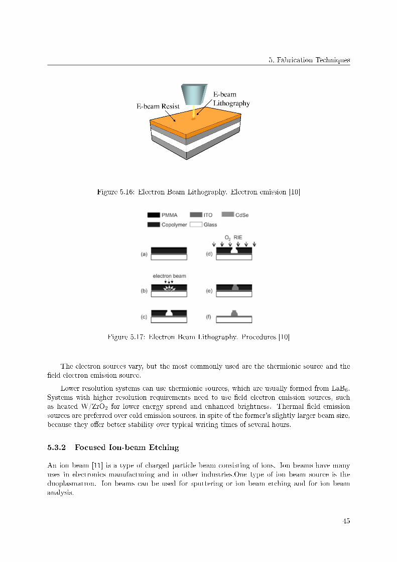
5. Fabrication Techniques
Figure 5.16: Electron Beam Lithography. Electron emission [10]
Figure 5.17: Electron Beam Lithography. Procedures [10]
The electron sources vary, but the most commonly used are the thermionic source and the�eld electron emission source.
Lower resolution systems can use thermionic sources, which are usually formed from LaB6.Systems with higher resolution requirements need to use �eld electron emission sources, suchas heated W/ZrO2 for lower energy spread and enhanced brightness. Thermal �eld emissionsources are preferred over cold emission sources, in spite of the former's slightly larger beam size,because they o�er better stability over typical writing times of several hours.
5.3.2 Focused Ion-beam Etching
An ion beam [11] is a type of charged particle beam consisting of ions. Ion beams have manyuses in electronics manufacturing and in other industries.One type of ion beam source is theduoplasmatron. Ion beams can be used for sputtering or ion beam etching and for ion beamanalysis.
45
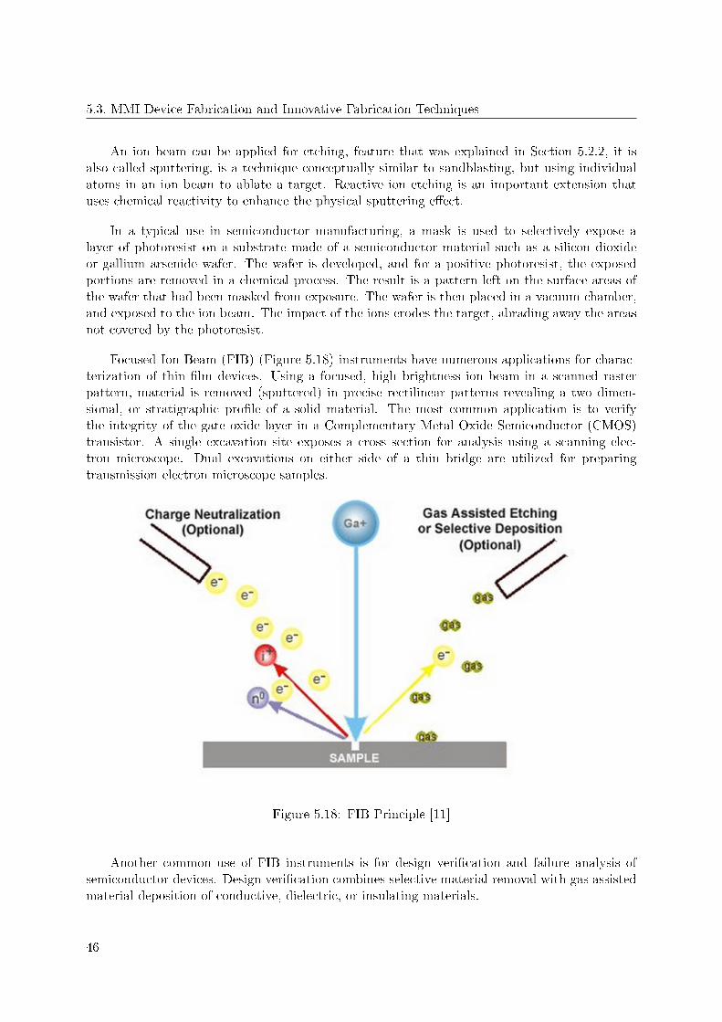
5.3. MMI Device Fabrication and Innovative Fabrication Techniques
An ion beam can be applied for etching, feature that was explained in Section 5.2.2, it isalso called sputtering, is a technique conceptually similar to sandblasting, but using individualatoms in an ion beam to ablate a target. Reactive ion etching is an important extension thatuses chemical reactivity to enhance the physical sputtering e�ect.
In a typical use in semiconductor manufacturing, a mask is used to selectively expose alayer of photoresist on a substrate made of a semiconductor material such as a silicon dioxideor gallium arsenide wafer. The wafer is developed, and for a positive photoresist, the exposedportions are removed in a chemical process. The result is a pattern left on the surface areas ofthe wafer that had been masked from exposure. The wafer is then placed in a vacuum chamber,and exposed to the ion beam. The impact of the ions erodes the target, abrading away the areasnot covered by the photoresist.
Focused Ion Beam (FIB) (Figure 5.18) instruments have numerous applications for charac-terization of thin �lm devices. Using a focused, high brightness ion beam in a scanned rasterpattern, material is removed (sputtered) in precise rectilinear patterns revealing a two dimen-sional, or stratigraphic pro�le of a solid material. The most common application is to verifythe integrity of the gate oxide layer in a Complementary Metal Oxide Semiconductor (CMOS)transistor. A single excavation site exposes a cross section for analysis using a scanning elec-tron microscope. Dual excavations on either side of a thin bridge are utilized for preparingtransmission electron microscope samples.
Figure 5.18: FIB Principle [11]
Another common use of FIB instruments is for design veri�cation and failure analysis ofsemiconductor devices. Design veri�cation combines selective material removal with gas assistedmaterial deposition of conductive, dielectric, or insulating materials.
46

5. Fabrication Techniques
Engineering prototype devices may be modi�ed using the ion beam in combination withgas assisted material deposition in order to rewire an integrated circuit's conductive pathways.The techniques are e�ectively used to verify the correlation between the Computer Aided Design(CAD) design and the actual functional prototype circuit, thereby avoiding the creation of a newmask for the purpose of testing design changes.
Sputtering is also used in materials science for extending surface analytical techniques suchas secondary ion mass spectrometry or electron spectroscopy so that they can depth pro�le them.
47

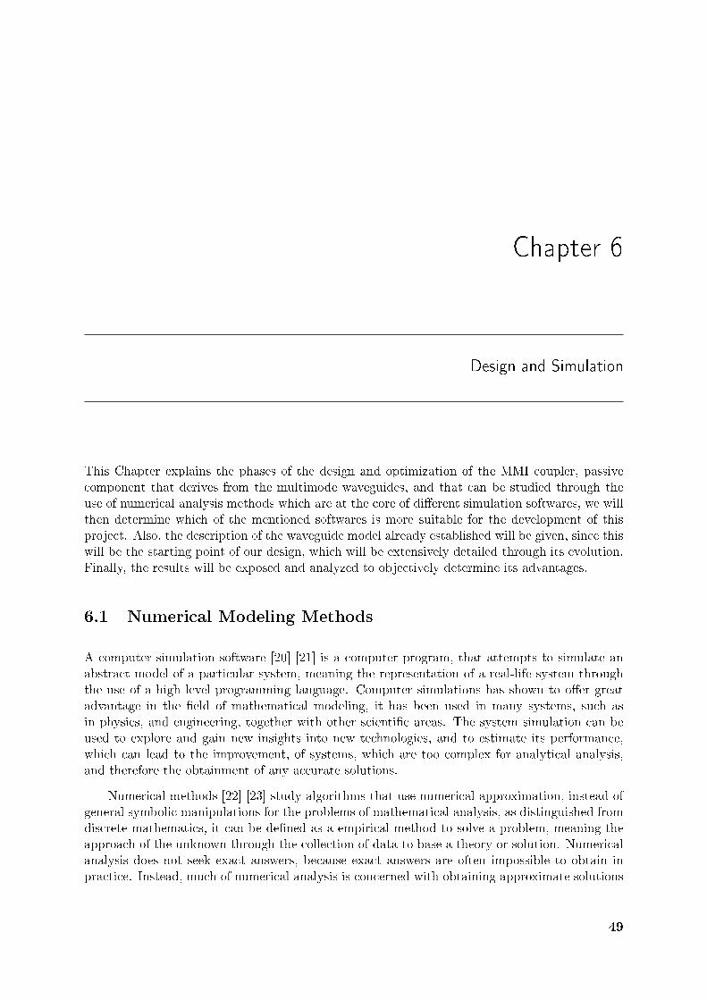
Chapter 6
Design and Simulation
This Chapter explains the phases of the design and optimization of the MMI coupler, passivecomponent that derives from the multimode waveguides, and that can be studied through theuse of numerical analysis methods which are at the core of di�erent simulation softwares, we willthen determine which of the mentioned softwares is more suitable for the development of thisproject. Also, the description of the waveguide model already established will be given, since thiswill be the starting point of our design, which will be extensively detailed through its evolution.Finally, the results will be exposed and analyzed to objectively determine its advantages.
6.1 Numerical Modeling Methods
A computer simulation software [20] [21] is a computer program, that attempts to simulate anabstract model of a particular system, meaning the representation of a real-life system throughthe use of a high level programming language. Computer simulations has shown to o�er greatadvantage in the �eld of mathematical modeling, it has been used in many systems, such asin physics, and engineering, together with other scienti�c areas. The system simulation can beused to explore and gain new insights into new technologies, and to estimate its performance,which can lead to the improvement, of systems, which are too complex for analytical analysis,and therefore the obtainment of any accurate solutions.
Numerical methods [22] [23] study algorithms that use numerical approximation, instead ofgeneral symbolic manipulations for the problems of mathematical analysis, as distinguished fromdiscrete mathematics, it can be de�ned as a empirical method to solve a problem, meaning theapproach of the unknown through the collection of data to base a theory or solution. Numericalanalysis does not seek exact answers, because exact answers are often impossible to obtain inpractice. Instead, much of numerical analysis is concerned with obtaining approximate solutions
49

6.1. Numerical Modeling Methods
while maintaining reasonable bounds on errors. Numerical analysis naturally �nds applicationsin all �elds of engineering and the physical science. Numerical stability is the most desirableproperty seeked in numerical algorithms. Other critical characteristics of a numerical computinganalysis method is the accuracy, the rate of convergence and the e�ciency.
As explained previously, numerical analysis is an essential component of modern science andengineering, for the modeling of numerous technologies and theories. On the following sections wewill mention a collection of software programs available for numerical simulations of waveguidingstructures. The software is divided into two major categories of our concern: Mode Solvers,Wave Propagators.
6.1.1 Mode Solvers
Modes [24] are the �elds that maintain the same transverse distribution and polarization at alldistances along the waveguide axis. For a limited number of ideal, simple waveguide con�gura-tions, modes and corresponding propagation constants can be found analytically. However, for amajority of realistic waveguides, numerical simulations are essential. Even the waveguides withrelatively simple cross-sections and refractive index pro�les in reality may su�er from anisotropy,inhomogeneities due to fabrication tolerances, and material losses that a�ect their modal prop-erties. Depending on the refractive index pro�le and other waveguide characteristics, varioustypes of modes may be supported, including antiguiding, leaky, lossy, or radiating modes.
This section contains several mode solvers based on numerical techniques of di�erent com-plexity and specialization. Some of the tools can simultaneously be used as mode solvers and aswave propagators (Transfer-Matrix Method, Eigenmode Expansion Method, Beam PropagationMethod, Finite Element Method), while others are Mode Solvers only (Plane Wave ExpansionMethod, Multipole Method, Source Model Technique). While some of the numerical methods,such as the Finite Element Method, the Plane Wave Expansion Method, the Beam Propaga-tion Method-based mode solvers, the Film Mode Matching Method, and the Finite-Di�erenceMethod, can be used for �nding modes of the arbitrary cross-section and refractive index pro-�le waveguides, others are more specialized. For instance, the Multipole Method (CUDOS MOFUtilities) and the Source Model Technique (developed by Professor Leviatan's group at Technion)are techniques that are particularly useful mode-�nding modes of microstructured or photoniccrystal �bers.
There are also methods that include several software packages that comprise more than onemode-solving technique (FIMMWAVE Mode Solvers by Photon Design, MODE Solutions byLumerical, OlympIOs Mode Solver Modules by C2V, OptiFIBER by Optiwave). These packagesinclude various techniques, ranging from approximate analytical methods, including the E�ec-tive Index Method and the Marcatili's Method (OlympIOs Mode Solver Modules by C2V), andthe Gaussian Mode Fiber Solver (FIMMWAVE Mode Solvers), to advanced numerical meth-ods, such as the semi-vectorial and full-vectorial Finite-Di�erence Method (MODE Solutions,OlympIOs Mode Solver Modules, OptiFIBER by Optiwave), the Film Mode Matching Method(FIMMWAVE Mode Solvers by Photon Design, OlympIOs Mode Solver Modules), the Transfer-Matrix Method (OptiFIBER by Optiwave), and the Finite Element Solver (FIMMWAVE ModeSolvers by Photon Design). Depending on the problem, required accuracy and simulation speed,the user can choose an appropriate method. The following methods only use a single numerical
50

6. Design and Simulation
tool, the Beam Propagation Method-based mode solvers, utilizing the iterative method and thecorrelation method (BeamPROP Mode Solvers by RSoft), and the Wave Matching Technique(developed by Dr. Hammer at the University of OsnabrÃ1
4ck).
6.1.1.1 Finite Element Method (FEM)
The FEM [25] [24] methods have been implemented in both time and frequency domains, andcan be used as wave propagators and mode solvers simultaneously. However, some of the FEMsoftware packages work only as mode solvers and should not be confused with those allowingpropagation e�ects studies (FEMSim by RSoft, FIMMWAVE-FEM-Solver by Photon Design,pdnMesh free software).
The FEM is a numerical technique for �nding approximate solutions to Partial Di�erentialEquations (PDE) and their systems as well as integral equations, that handle complex geometries,and boundaries, such as waveguides with arbitrary cross-sections, with relative ease. The �eldregion is divided into elements of various shapes, such as triangles and rectangles, allowing theuse of an irregular grid, in simple terms, it divides up a very complicated problem into smallelements that can be solved in relation to each other. The solution approach is based either oneliminating the di�erential equation completely (steady state problems), or rendering the PDEinto an equivalent ordinary di�erential equation, which is then solved using standard techniques,such as �nite di�erences. In a context of optical waveguides, the FEM can be used for modesolving and propagation problems. Two approaches to solve waveguide problem include thevariational method and the weighted residual (Galerkin) method. Both methods lead to thesame eigenvalue equation that needs to be solved.
6.1.1.2 EigenMode Expansion Method (EMEM)
The EMEM [24] is based on a rigorous solution of Maxwell's equations, representing the electro-magnetic �elds everywhere in terms of a basic set of local modes. In principle an exact solutioncan be obtained using an in�nite number of modes in our expansion. Of course, in practice thenumber of modes is limited and there will be numerical errors in the implementation, as in anynumerical technique. To obtain higher accuracy one can simply add more modes, enabling themethod to accurately compute problems that cannot be computed with other techniques. Thealgorithm is inherently bi-directional and utilizes the scattering matrix (S-matrix) technique tojoin di�erent sections of the waveguide or to model nonuniform structures. The scattering matrixtechnique relates the incoming waves, i.e. the forward wave at the beginning of the section andthe backward wave at the end of the section, to the outgoing waves, i.e. the backward wave atthe beginning and the forward wave at the end. All re�ections are taken into account in themethod. If one part of a device is altered, only the S-matrix of that part needs to be re-computed.The method can simulate light propagating at any angle, even 90 degrees to the propagationaxis, simply by adding more modes. Applications include di�ractive elements, directional cou-plers, tapers, MMIs, bend modeling, periodic structures and others. Structures with a very largecross-section are less suitable for the method since computational time typically scales in a cubicfashion, with, for example, cross-section width.
51

6.1. Numerical Modeling Methods
CAvity Modelling FRamework (CAMFR) is a commonly used simulation program, it is aFull-vectorial Maxwell solver based on the EMEM. Although it can handle general electromag-netic problems, its main focus is on applications in the �eld of photonics. CAMFR treats the�eld as a sum of local eigenmodes in each z-invariant layer and does not rely on spatial discretisa-tion and �nite di�erences to solve Maxwell's equations, as other methods, like Finite-Di�erenceTime-Domain (FDTD) 6.1.2.5, do.
Since there is no spatial discretisation, CAMFR can be orders of magnitude faster thanFDTD for a large class of structures. Incorporates advanced boundary conditions, which candrastically improve simulation accuracy and speed.CAMFR is an ongoing active research project.Two-dimensional Cartesian structures and three-dimensional cylindrical symmetric structuresCAMFR can be used to calculate the scattering matrix of a structure, the �eld inside a struc-ture, for any given excitation, the band diagrams of an in�nite periodic structure, the thresholdmaterial gain and resonance wavelength of laser modes, and the response to a current source inan arbitrary cavity.
De�ning structures is quite straightforward, either layer-by-layer, or using geometric primi-tive shapes. There are also integrated plotting routines for rapid simulation feedback. CAMFR isconceived as a C++ framework, with all the algorithms implemented in terms of abstract waveg-uides and scatterers. This makes it extremely easy to extend CAMFR to new geometries. Theend user does not deal with this C++ code directly, but rather through bindings to the Pythonscripting language. It is specialized in the simulation of wavelength-scale microstructures (likephotonic crystal devices), lasers (like vertical-cavity surface-emitting lasers) and light-emittingdiodes (like resonant-cavity Light Emitting Diodes (LED)s).
Another simulation tool is FIMMPROP, a highly innovative tool for simulating propagationin optical waveguides in 2D and 3D, which is fully integrated as part of FIMMWAVE, a genericfull vectorial optical mode solver for waveguide structures, and relies on the rigorous EMEM.
The EMEM enables the �elds to be calculated using fast semi analytical methods. Thespeed and nature of the calculations allow the propagation to be treated in a fully bi-directionalmanner, taking into account all the re�ections at intermediate joints. This makes FIMMPROPcapable of modeling structures which are insolvable by other methods such as BPM.
It is used in the modeling of devices with strong internal re�ections, such as waveguidesterminated by a tilted facet. Use of semi-analytical modal methods by FIMMPROP permitscalculations to achieve high accuracy even for more complicated structures.Calculations permitboth transmission and re�ection coe�cients of the modes at each joint to be determined foruse in the fully bi-directional propagation algorithm. Structures with Z-varying cross-sectionssuch as tapers and Y-junctions are computed using sophisticated extensions to the EMEM. Thealgorithm builds a scattering matrix description of the device and all its elements, which meansthat once the matrices are generated, the response to many di�erent input pro�les can be foundwithout further computation, for example to obtain response to both TE and TM excitation. Ifthe structure is altered, the routine needs only recalculate the elements that have changed.
It is used to model devices and components like the MMI couplers, Mode converters, Codi-rectional couplers (polarization converters), Bends, Periodic structures, Tilted joins, Facets andfree space regions for waveguide-gap-�ber simulations.
52
6. Design and Simulation
6.1.1.3 Full-Vectorial Finite-Di�erence Method (FV-FDM)
The full-vector �nite di�erence mode solver [24] analyses micro-structured optical �bers. It isa new mode solver, a hybrid, that is based on discretization scheme was �rst proposed by Yee.Yee's mesh is widely used in the FDTD analysis. In the FV-FDM the Yee's two-dimensionalmesh is used for complex optical waveguides. It is widely used for the modeling of MMI couplers[26] [27] . It permits the determination of the working principle of devices and to evaluate theirperformance. It can be directly utilized for evaluating e�ective refractive index distributions,as well as eigenmode characteristics, and the calculation of e�ective indexes of the TE and TMpolarized modes.
It shows an improvement for all of the Finite Di�erence mode solvers and is particularlye�ective when combined with Yee's mesh. This results in signi�cantly accelerated convergenceand improved numerical accuracy. The validity and e�ectiveness of this mode solver is the reasonfor its high usage in the MMI device simulation.
6.1.1.4 Full-Vector Finite-Element Beam Propagation Method (VFE-BPM)
The VFE-BPM [28] , is another hybrid which uses both wave propagation analysis and modesolvers. In terms of all the components of slowly varying electric �elds is described for the analysisof 3D nonlinear optical waveguides. Electric �elds obtained with this approach can be directlyutilized for evaluating nonlinear refractive index distributions. To eliminate nonphysical, spurioussolutions, hybrid edge/nodal elements are introduced. Furthermore, to avoid spurious re�ectionsfrom the computational window edges, anisotropic perfectly matched layer boundary conditionsare implemented, and to reduce computational e�ort for the nonlinear optical waveguide analysis,an iterative algorithm is also introduced. The e�ectiveness of the present approach is veri�ed byway of numerical examples: nonlinear directional couplers, spatial soliton emission phenomena,and soliton couplers.
The method is useful for analysis of a three-dimensional nonlinear optical waveguide isnewly developed with all slowly varying electric �eld components as unknown variables. Thederived electric �eld can be used directly for evaluation of the nonlinear refractive index, sothat a nonlinear refractive index directly corresponding to the electric �eld can be obtained.Various methods are included for improving the performance of the VFE-BPM such as theedge/nodal hybrid elements for suppressing generation of spurious solutions, the anisotropicperfectly matched layer for prevention of spurious re�ection from the analysis domain edges, andan iteration method to relax the step width in the propagation direction.
6.1.2 Wave Propagators
Wave propagation techniques [24] are essential components of waveguide and waveguide-basedphotonic device design. While mode-solving methods are based on the assumption that theguiding structures are uniform in the propagation direction, many practical waveguide con�gu-rations, such as tapers, bends and junctions, are actually nonuniform in the longitudinal direc-tion. The analysis of these types of waveguides relies on propagation-type techniques. Even in
53

6.1. Numerical Modeling Methods
uniform structures, propagation methods provide important information about beating betweenmodes in multimode structures, mode �ltering upon propagation, and mode coupling e�ects. Inaddition, propagation methods facilitate numerical studies, accurately re�ecting wave guidingproperties of realistic devices and providing insight into the �eld's evolution inside the structure.In these simulations arbitrary launch conditions are usually allowed and the evolution of such anarbitrary beam/pulse can be monitored at any point inside the structure. This section includesboth time-domain methods, including the FDTD, the Split-Step Method (SSM), and the FEM,and frequency-domain methods, such as the BPM, the Transfer Matrix Method (TMM), and theEMEM.
6.1.2.1 SSM
The SSM [24] is a Nonlinear Schrodinger Equation Solver provided by Professor Agrawal's groupat the Institute of Optics , University of Rochester , OptSim by RSoft, SSPROP provided byProfessor Murphy, University of Maryland , College Park. It is a simple and straightforwardtechnique for the modeling of linear and nonlinear pulse propagation of optical �bers. It allowsthe inclusion of all major e�ects taking place in realistic optical �bers, including group-velocitydispersion and higher-order dispersion, self-phase modulation, cross-phase modulation, four-wavemixing e�ects, Raman ampli�cation and many other linear and nonlinear phenomena.
6.1.2.2 TMM
The TMM [24] (GratingMOD by RSoft, OptiGrating by Optiwave, TMM Mode Solver andAnisotropic TMMMode Solver developed by Henri Uranus at the University of Twente, WAVEG-UIDE provided by the Southern Methodist University group) and the EME (CAMFR developedby Ghent University group, FIMMPROP by Photon Design, OlympIOs Bidirectional EigenmodePropagation Module) methods are relatively simple methods that are inherently bidirectional.They are especially useful for the modeling of waveguides comprising grating structures, waveg-uide tapers and couplers.
6.1.2.3 BPM
The BPM [24] (implemented in BeamPROP by RSoft, OlympIOs by C2V, OptiBPM by Op-tiwave, OptoDesigner by PhoeniX) is a widely used and well-developed method that solveswave propagation problems for a given frequency. Several advanced techniques, including semi-vectorial and vectorial implementations, wide-angle and bi-directional BPM, have been devel-oped, making the BPM a versatile technique for a wide class of optical waveguides with arbitrarycross-sections and complex refractive index pro�les. It is the most commonly used method inMMI devices simulation, since it takes all modes into account, including radiative modes, andtherefore provides the most accurate model for most optical devices.
The BPM was developed for the analysis of light propagation in slowly varying nonuniformguiding structures, such as tapers, bends, and couplers. Various implementations of BPM di�er
54

6. Design and Simulation
by the method used for calculations of the derivatives with respect to the coordinates in the prop-agation directions and include the Finite-Di�erence Beam Propagation Method (FD-BPM), FastFourier Transformer Beam Propagation Method (FFT-BPM), and the Finite-Element BeamPropagation Method (FE-BPM). Historically, the FFT-BPM was widely used until the FD-BPMwas developed. The standard form of implementation of the FD-BPM is the Crank-Nicholson method. The standard BPM solves the Helmholtz equation in paraxial approximation.
The paraxial approximation enables BPM to analyze much longer structures (on the mil-limeter and centimeter scale) than would be realistic for analysis with FDTD. While the BPM isusually used for the modeling of low-index-contrast waveguides, some relatively high-index con-trast structures can be studied as well. Scalar, semi-vectorial, and vectorial formulations havebeen developed, and several advanced features have been proposed and implemented in BPM-based software packages, including wide-angle formulation and bi-directional propagation. TheBPM versions that incorporate nonlinearities, anisotropy, gain and loss have been described andimplemented. In addition, two BPM-based mode solvers (based on imaginary-distance BPMand correlation technique) have been proposed. Typical BPM applications include standard,specialty, and photonic crystal �bers, switches, modulators, multimode interference devices, andpassive splitters.
BeamPROP [29] is the industry-leading design tool based on the BPM for the design andsimulation of integrated and �ber-optic waveguide devices and circuits. The software has beencommercially available since 1994, and is in use by leading researchers and development engineersin both university and industrial environments worldwide. It has been proven to be a topalgorithm for fast and accurate device design. The BeamPROP also has a built-in advancedAWG utility for simplifying router and demultiplexer design. Advanced capabilities allow for thesimulation of complicated devices, and it is fully integrated into the RSoft CAD Environment.
BeamPROP has applications in a wide range of integrated and �ber-optic devices including,but not limited to:
• Wavelength-Division Multiplexing (WDM) devices such as Arrayed Waveguide Grating(AWG) routers.
• Switches, like the directional coupler-based or digital-y type.
• Modulators, for example the Mach-Zehnder type
• Multimode interference devices.
• Passive 1xN or NxN splitters.
• Laser structure transverse mode analysis
• Standard and specialty �ber design.
• Gratings
• Sensor structures.
55
6.1. Numerical Modeling Methods
The BeamPROP delivers superior robust and e�cient results based on an implicit �nite-di�erence scheme. It has numerous features, such as:
• 2D and 3D simulation capabilities.
• Non-uniform mesh.
• Anisotropic and non-linear materials.
• Electrode and heater e�ects.
• Polarization e�ects and coupling via a full-vectorial BPM implementation.
• Wide-angle propagation can be improved by multistep Padé approximation techniques,a variable reference wave number, and conformal index mapping of bends to allow foraccurate and e�cient o�-axis propagation.
• Bidirectional BPM formulation for considering re�ection along the propagation directionto be considered.
• Two BPM-based mode-solvers for the computation of modal propagation constants andpro�les for both guided and radiation modes for 2D and 3D geometries.
• Comprehensive measurement tools to compute �elds, power distribution, loss, etc.
6.1.2.4 Finite-Di�erence Method (FDM)
The FDM [30] is a numerical methods for approximating the solutions to di�erential equationsusing �nite di�erence equations to approximate derivatives. The FDM relies on discretizing afunction on a grid. To use the �nite di�erence method to attempt to solve (or, more generally,approximate the solution to) a problem, one must �rst discretize the problem's domain. This isusually done by dividing the domain into a uniform grid.
The previous explained procedure leads the �nite-di�erence methods to produce sets ofdiscrete numerical approximations to the derivative, which generally can create errors. Thiserror in a method's solution is de�ned as the di�erence between its approximation and the exactanalytical solution.A �nite di�erence is a mathematical expression of the form f(x+b)−f(x+a). If a �nite di�erence is divided by b− a , one gets a di�erence quotient. The approximation ofderivatives by �nite di�erences plays a central role in �nite di�erence methods for the numericalsolution of di�erential equations, especially boundary value problems. The two sources of errorin �nite di�erence methods are round-o� error, the loss of precision due to computer rounding ofdecimal quantities, and truncation error or discretization error, the di�erence between the exactsolution of the �nite di�erence equation and the exact quantity assuming perfect arithmetic.
56
6. Design and Simulation
6.1.2.5 FDTD Method
The FDTD [31] [24] is a numerical analysis technique used for modeling computational electrody-namics, it is implemented in a large number of free and commercially available packages, it is themost general and rigorous time-domain method, and because of this characteristic this system is�t to cover a wide range of frequencies with just one simulation run. It is particularly useful fora large number of optical guiding structures, such as photonic crystal waveguides, surface plas-mon waveguides, high-index contrast waveguide devices, ring and disk resonators, negative indexmaterial structures, dispersive, and nonlinear materials since it tries its properties in a naturalway. Modal properties can be extracted after a single propagation. However, the FDTD maybecome prohibitively computationally intensive and therefore impractical for long waveguidesand devices.
The FDTD technique is based on a discrete representation of time-dependent Maxwell'sequations on a grid that is exact in the limit that the grid spacing goes to zero. Various opti-cal materials can be used with FDTD algorithms. Current FDTD modeling applications rangefrom near-DC (ultralow-frequency geophysics involving the entire Earth-ionosphere waveguide)through microwaves (radar signature technology, antennas, wireless communications devices, dig-ital interconnects, biomedical imaging/treatment) to visible light (photonic crystals, nanoplas-monics, solitons, and biophotonics).
Modal properties can be extracted in a single simulation by Fourier-transformation of thetime-varying response of the system to some input. Then, the peaks in the resulting spectrumcorrespond to the eigenfrequencies. The primary limitation of FDTD is that it is computationallyintensive, especially in the three-dimensional case, but the method is readily applicable to thetwo-dimensional structures. In practice, FDTD needs to have at least 10 to 20 cells per minimumwavelength in every direction, depending on the application and accuracy required. Also, evenhigher sampling rates may be required to reduce the cumulative numerical dispersion error,which is proportional to the length of wave propagation. This renders FDTD impractical forlarge devices.
Various techniques have been proposed to make the FDTD method more e�cient, includ-ing pseudospectral time-domain techniques, nonuniform and adaptive mesh re�nement, hy-brid FDTD-Finite Element techniques, and hardware acceleration concepts. Di�erent softwareproviders take various approaches to optimize the performance of their software in solving prob-lems that require clustering. The approaches include parallel processing features in the softwareand, most recently, dedicated hardware to increase single system processing speeds. Typicalapplications for optical software based on an FDTD algorithm include the modeling of high-index-contrast waveguides, photonic-bandgap structures for photonic crystals, ring resonators,nano-plasmonic devices, gratings and other di�ractive structures, dispersive, nonlinear and gainmaterials, and biophotonics.
6.2 Waveguide Model
Fraunhofer IZM with previous work has already established a general structure for the compo-nents in its optical circuits, and therefore the passive component that will be developed in this
57

6.2. Waveguide Model
project shall follow this basic speci�cations. The description given will detail both for Singlemode and for Multi mode waveguides the layer materials and primary dimensions. This willallow its future incorporation into more complex circuits with as much simplicity as possible.For the same reasons all designs where made in 3D, despite the fact that these devices havethe same behavior through the whole transversal direction, permitting the obtainment of similarresults with a 2D design.
6.2.1 Single Mode Waveguide
In Chapter 2 the waveguide characteristics where exposed and detailed since the design is basedon the SOI slab waveguide with a ridge etched into the upper substrate,changing the e�ectiveindices of refraction on either side, creating conditions for Total internal re�ection (TIR) to occurwithin the ridge area allowing for guidance of light. The materials to be used are shown in Table6.1 together with their respective index, and the dimensions and arrangement of each layer inFigure 6.1 .
Material Refractive Index
Air 1Silicon 3.48
Silicon Dioxide 1.46
Table 6.1: Materials and Refractive index of the Optical Waveguide
Figure 6.1: Single Mode Cross Section of the Waveguide
Where through a vetical cut we will have by order the Cover of the wave guide is the Air
theoretically in�nite, followed by the Ridge and Slab composed by Si (Silicon) that measure290nm and 50nm respectively. Afterwards we encounter the Insulator formed by SiO2 (SiliconDioxide) which, as its name dictates, to isolate the Slab it must have a large vertical dimensiontherefore measuring 2µm. Finally the waveguide ends with the Silicon substrate layer which isalso theoretically in�nite.
58

6. Design and Simulation
Horizontally the only limited layer is the Ridge which will be of 400nm and will be con�nedlaterally and in the upper surface by the Air as shown in the mentioned �gure.
The Single mode waveguides represent the inputs and the outputs (Figure 6.2) of the MMIdevice, and initially it will be used uniquely for this purpose.
Figure 6.2: Design Layout. Input Single mode Waveguides, MMI Section, Output Single modeWaveguides [4]
6.2.2 Multi Mode Waveguide
The Multi Mode Waveguide represents the MMI section of the device shown in Figure 6.2 .Its di�erence with the Single Mode Waveguide relies only in the width of the Ridge since thischaracteristic will determine its Multi Modal properties. Its cross section is shown in Figure 6.3.
In respect to the materials used as seen in the previously mentioned �gure it remains equalto the ones used in the Single Mode Waveguide, as the vertical dimensions are maintained thesame. The width of the Ridge is arbitrary but to obtain a optimized result simulations must beperformed keeping in mind that for the Multi Mode characteristics to prevail the width of thislayer must not decrease from a certain point.
6.3 Design and Simulation
The MMI Coupler to be design will only cover, from the basic cases of self-imaging which wecan observe in Figure 6.4, the Paired and Symmetric interference mechanism, leaving out theGeneral interference case.
59

6.3. Design and Simulation
Figure 6.3: Multi Mode Cross Section of the Waveguide
This cases follow the formulas encountered in the �gure and in Chapter 4. We can see thesummary of analytical characteristics in Table 6.2 . From the mentioned cases we will designand simulate the 1x2, the 1x3, and the 2x2 coupler (Figures 6.5, 6.6 and 6.7).
Interference Mechanism General Paired Symmetric
Inputs x Outputs NxN 2xN 1xNFirst single image distance 3Lπ Lπ (3Lπ)/4
First N fold image distance (3Lπ)/N (Lπ)/N (3Lπ)/4N
Excitation requirements none cv = 0 for v = 2, 5, 8, .. cv = 0 for v = 1, 3, 5, ..
Input(s) location(s) any y = ±We/6 y = 0
Table 6.2: Summary of Characteristics of the General, Paired and Symmetric Interference Mech-anisms
6.3.1 Initial Design
The initial design of the MMI Coupler shall follow the standards detailed previously, but thede�nition of the cross section for practical reasons will be modi�ed as shown in Figure 6.8,eliminating the last silicon layer, which will not change the result, since the Silicon Dioxidesubstrate layer has the task of avoiding any in�uence of this mentioned layer with the functionof the MMI device.
To do such a modi�cation the global description of the waveguides in the BeamPROP soft-ware simulator must be performed as shown in Table 6.3.
Our waveguide is designed in 3D therefore we must de�ne a structure type in the descriptionas well, �lling the Layer Table 6.4 as shown.
Afterwards, the MMI sections width (Wmmi) is arbitrarily determined, and since the widthand the length (Lmmi) of this segment are related through the beat length (Lπ) as noted inEquation 4.5, Figure 6.4, and the next Equations 6.1 and 6.2 .
60
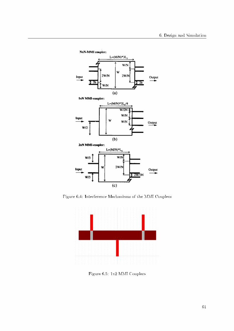
6. Design and Simulation
Figure 6.4: Interference Mechanisms of the MMI Couplers
Figure 6.5: 1x2 MMI Couplers
61

6.3. Design and Simulation
Figure 6.6: 1x3 MMI Couplers
Figure 6.7: 2x2 MMI Couplers
Figure 6.8: Modi�ed Layer Structure of the Waveguide
62

6. Design and Simulation
Parameter Value
Index Di�erence 2.02Background Index 1.46
Free Space Wavelength (µm) 1.55Waveguide Width (µm) 0.4Waveguide Height (µm) 0.34
Cover Index 1Slab Height (µm) 0.05
Table 6.3: Parameters of the Global Settings of the Waveguides in the BeamPROP SoftwareSimulator
Parameter Height (µm) Index
Cover ∞ 1Layer 2 0.29 3.48Layer 1 0.05 3.48Substrate ∞ 1.46
Table 6.4: Parameters for the Layer Table de�nition
L =
(M
N
)3Lπa
(6.1)
Where
a =
1 for NxN
4 for 1xN
3 for 2xN
(6.2)
Beginning with the veri�cation of the excitation of the wanted modes we simulated the1x3 MMI Coupler, obtaining the expected results of a Symmetric Interference, the excitation ofmodes 1, 3, 5,... (Figures 6.9, 6.10 and 6.11 respectively). This was performed by the use of theCompute Mode feature in BeamPROP. Then to run the simulation certain speci�cations had tobe speci�ed, such as:
Launch Field Field where as its name states, determines the point of the structure where theinput �eld should be launched, being this the Single Mode Input Waveguide. And from allthe possible �elds we use a Gaussian Beam.
Monitor This will measure the desired parameter, in our case the amplitude of the �eld, througha de�ned Path.
Path To determine this, we select the Input and Output, and a inactive segment with the outputthat travels through the theoretical position in with the mode will be excited as shown inFigures 6.6 and 6.12.
63

6.3. Design and Simulation
Polarization Which would be TE or TM. Both must be simulated.
Figure 6.9: mode 1 of the Waveguide
Figure 6.10: mode 3 of the Waveguide
By simulating the device with a arbitrary width (Wmmi) of 12µm we obtain that the lengthof the MMI section is in both cases very similar to the calculated by analytical methods, beingthe TM case practically equal. But the di�erence between the length of the MMI section forthe TE (Figure 6.13) polarized and the TM (Figure 6.14) polarized can not be ignored, thisdi�erence is a demonstration of the polarization dependency of the structure, characteristic thatrequires to be modi�ed and eliminated.
64

6. Design and Simulation
Figure 6.11: mode 5 of the Waveguide
Figure 6.12: mode excitation and its amplitude lateral �eld pro�les [4]
6.3.2 Polarization Independent Design
The encounter with a polarization dependent structure leads to take a careful look into thedimensions of the mentioned waveguide, meaning the ridge's height (h) and width(Wmmi), sothat then the length of the MMI will be modi�ed as well. The main objective is to obtain equallength beats, calculated with the two lowest order modes, for both polarizations (TE and TM),this is a result of di�erent propagation constant spacing of the fundamental and the �rst ordermode of the Multimode section.
4 Lπ = LTEπ − LTMπ (6.3)
One proposed solution [26] is based on the fact that 4Lπ is a function of the core's, meaningthe ridge's, dimensions. It is proposed to modify the height of the ridge (h) to make 4Lπ = 0 ,
65

6.3. Design and Simulation
Cases Lmmi (µm)
Analytical method 110.864TE Polarization 107.9TM Polarization 110.88
Table 6.5: Lengths of a Polarization Dependent MMI Coupler
Figure 6.13: Result of the TE 1x3 MMI Coupler simulation
Figure 6.14: Result of the TM 1x3 MMI Coupler simulation
this is based on the characteristics of the TM modes that are sensitive to the waveguide's heightdue to the strong con�nement to the major component of the electric �eld in the vertical direction
66

6. Design and Simulation
(y-direction) while the characteristics of the TE modes are not so sensitive to the height, sincethe major component of the electric �eld is in the lateral direction (x-direction). But as werecall in Table 6.6 the polarization that requires modi�cation to achieve independence is the TEpolarization, and therefore instead of varying the height of the ridge to with the TM is sensitiveand the TE polarization is not, we will modify the width of the ridge, where the TE polarizationis sensitive due to the strong con�nement of its major electric �eld component until we obtain a4Lπ = 0.
This solution has also been taken into account in another paper [12] , with successful results(Figure 6.15) where they state that by choosing a suitable core width the birefridgence in theslab waveguide will be balanced, and hence the polarization insensitive MMI coupler is achieved.
Figure 6.15: (a) Variation of beat length di�erence vs. core width. (b) Core width required toobtain 4Lπ = 0 vs. height (t) [12]
When simulated we obtain a polarization independent MMI coupler, the successful resultwas con�rmed after the collection of data from many simulations where we varied the width ofthe MMI section and measured the corresponding length. The results of each simulation run areshown in Table 6.6, and in Figure 6.16 permitting a easier comparison with the results in Figure6.15 (a) from the paper that proposed this solution.
As we can see the best result is 2.5 µm but after a more �ne simulation the optimum widthwas of 2.55µm. Also, we can appreciate in the table that the result from the simulations di�erfrom slightly from the theoretical prediction, this is due to the approximation of the self-imagingprinciple explained in Chapter 4 . This width results are applicable to all the MMI Couplersto be design, since it depends on the dimensions of the ridge, not on the number of inputs andoutputs.
6.3.3 Tapered Design
Though the problem with the polarization dependence was solved, another issue that requiresattention is still present, and it is at this point where a general view of all 3 designs must end,
67

6.3. Design and Simulation
Wmmi (µm) LTEmmi (µm) LTMmmi (µm) Theoretical Lmmi (µm) 4Lπ (µm)
2 3 2.79 3.079 -0.212.5 4.298 4.3 4.811 0.0023 6.06 6.18 6.929 0.124 30.58 30.94 12.318 0.366 42.9 44.6 27.716 1.710 61.96 67.6 76.989 5.64
Table 6.6: Lengths of a Polarization Dependent MMI Coupler
Figure 6.16: Variation of beat length di�erence vs. core width
since it is only in the 1x3 MMI Coupler design where we encounter this discrepancy, the presenceof Cross-talk (Figure 6.17 and 6.18) between the di�erent output SingleModed waveguides, con-sequence of the small size of the device's width, that creates a closeness that produces the leakageof power from one segment to another, mainly from the central output waveguide to the lateralones. In the 1x2 MMI this does not occur, and in the 2x2 MMI it can be solved in the splittingapplication without the use of tapered widths, but for the switching application, tapering mustbe used as well, since by the use of an parabolically or exponentially tapered section we mayincrease the distance between the outputs and thus eliminate the coupling (cross-talk) betweenthem.
An exponentially tapered width, as the one applied to the 1x3 MMI Coupler, shown in Figure6.19 , and a parabolical one (Figure 6.20) used on the 2x2 switch MMI Coupler, are useful notonly for the mentioned reason, but also it permits the compactness of the device through theshortage of the MMI sections length. In addition tapering the width increases the light intensitynear the dielectric corners, with abrupt discontinuities, becomes smaller, and consequently there�ection is reduced. By all these means the increasing of the tapered width can improve thequality of self-imaging, and thus reduce the Excess Loss (EL).
68

6. Design and Simulation
Figure 6.17: Cross-talk of the MMI Coupler's outputs
Figure 6.18: Cross-talk of the MMI Coupler's outputs. Amplitude pro�les
When simulated the results obtained improved from the cross-talk perspective (Figure 6.21),but the existence of high loss and unbalance between the outputs was still a present problem,which was shared with the 1x2 MMI coupler and the 2x2 MMI coupler applied for spliting power.
69
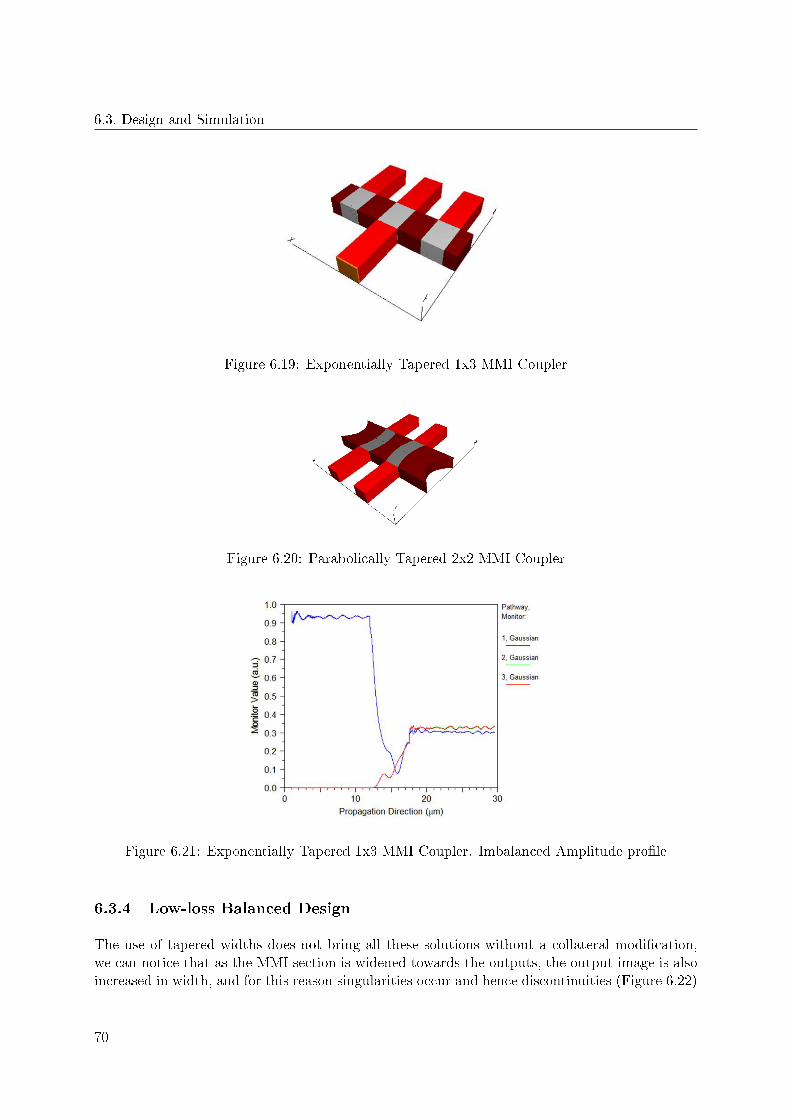
6.3. Design and Simulation
Figure 6.19: Exponentially Tapered 1x3 MMI Coupler
Figure 6.20: Parabolically Tapered 2x2 MMI Coupler
Figure 6.21: Exponentially Tapered 1x3 MMI Coupler. Imbalanced Amplitude pro�le
6.3.4 Low-loss Balanced Design
The use of tapered widths does not bring all these solutions without a collateral modi�cation,we can notice that as the MMI section is widened towards the outputs, the output image is alsoincreased in width, and for this reason singularities occur and hence discontinuities (Figure 6.22)
70

6. Design and Simulation
creating loss in the output.
The imbalance [32] [33] and excess loss in MMI couplers is primarily determined by theway the input power is partitioned into the MMI section modes. Because of this and the factsexplained in the previous Section 6.3.3 we introduce linear width tapers between the MMI sectionand the input-output waveguides (Figure 6.23), called access waveguide, with a taper lengthlong enough to be adiabatic, meaning that it provides an acceptable transition, this improvesthe image quality further making the imaged �eld match well with the fundamental mode of theoutput waveguides.
The partitioning previously mentioned is in turn determined by the normalized access waveg-uide width and position. There exists a number of optimum access waveguide widths that givea minimum imbalance. In particular, paired interference couplers are found to have better im-balance performance.
The imbalance between 2 outputs is determined by Equation 6.4, and the EL by Equation6.6 .
imbalance = 10 log1 0
(P1
P2
)(6.4)
EL = 10 log1 0
(P1 + P2 + P3 + ...
1
)(6.5)
It is recommended [34] , so that the results obtained have a level of requirement, to consideronly acceptable the EL < 0.5 dB, and in respect to the imbalance, which is certain cases has apredominant importance, for example in the MZI, to be < 0.2 dB. The results obtained withoutthe use of the linear taper access waveguide are the following (Table 6.7 for the TE polarizationand Table 6.8 for the TM polarization).
Input Output P1 P2 P3 Imbalance TE (dB) ELTE (dB)
1x3 0.241 0.282 0.241 0.682 1.1691x2 0.413 0.413 - 0 0.83
2x2switch 0.723 0.005 - - 1.372x2split 0.404 0.375 - 0.323 1.084
Table 6.7: Imbalance and EL of a width tapered MMI Coupler. TE polarization
Input Output P1 P2 P3 Imbalance TM (dB) ELTM (dB)
1x3 0.309 0.313 0.309 0.055 0.311x2 0.479 0.479 - 0 0.186
2x2switch 0.889 0.006 - - 0.4812x2split 0.491 0.491 - 0 0.078
Table 6.8: Imbalance and EL of a width tapered MMI Coupler. TM polarization
71

6.3. Design and Simulation
We can see that all the TE polarization results have a very elevated EL, over the level ofstandards, when on the TM polarization the results are very satisfactory, an so we take thesolution previously proposed of the implementation a access waveguided.
As this problem was present in all the designs, the 1x3 MMI coupler, the 1x2 MMI coupler,and the 2x2 MMI coupler applied for spliting power and for switching, the linear tapered accesswaveguide solution was applied to all of them.
Figure 6.22: 1x3 MMI Coupler. Discontinuities
Figure 6.23: 1x3 MMI Coupler with linear tapered access waveguides
When simulated the result is satisfactory as shown in the following section, together withthe ones from the rest of the designs.
72

6. Design and Simulation
6.4 Final Results
Besides all the important parameters to be de�ned mentioned in the previous section, we haveone that is of extreme value to the MMI Coupler, since its one of its advantages against othercouplers that could perform the same tasks, this parameter called the Fabrication Tolerance(FT)), determines the marge of error that the device, as its name states, tolerates for eachdimension, in this case the width and the length of the MMI section. In addition the Polarization-Dependent Loss (PDL) parameter (Equation 6.6) is also calculated for utility reasons in certainapplications and its the di�erence between the EL obtained in each polarization.
PDL = |ELTM − ELTE | (6.6)
The following �gures show the designs of all the MMI Couplers (Figure 6.24).
Figure 6.24: MMI Coupler Designs. 1x3(up-left), 1x2(up-right), 2x2split (down-left), and2x2switch (down-right)
We can observe in the �gure that both width tapered couplers, 1x3 exponentially, and2x2switch parabolically, require that the linear tapered access waveguides to have a similar angleto the tapering to avoid the presence of more discontinuities. In the 2x2split coupler design theposition of the inputs and outputs were modi�ed, by separating them we avoided the cross-talkbetween the outputs and we obtained the images at the output in the same position as the inputswithout major disruptions.
Also we observe a di�erence in many parameters on the design, some obtained by result ofthe simulations optimization (for example Lmmi and Wmmi) , and others like the tapered widthof the MMI section (Wmmi1), and the width (Wtap) and length Ltap of the linear tapered access
73

6.4. Final Results
waveguide were determined by running simulations in with they where varied until the mostoptimum result was obtained, these are:
1x3
Lmmi = 5.66µm
Wmmi = 2.53µm
Wmmi1 = 3.5µm
Ltap = Lmmi
Wtap = 0.75µm
(6.7)
1x2
Lmmi = 6.48µm
Wmmi = 2.5µm
Ltap = 10µm
Wtap = 0.65µm
(6.8)
2x2switch
Lmmi = 20.705µm
Wmmi = 2.55µm
Wmmi1 = 3.2µm
Ltap = 10.345µm
Wtap = 0.63µm
(6.9)
2x2split
Lmmi = 26.603µm
Wmmi = 2.55µm
Ltap = 10µm
Wtap = 0.6µm
(6.10)
The use of tapered widths waveguides produces changes in the dimensions of the device, forexample the length of the MMI section, as we can observe in the previously delivered results.
The �nal result Figures 6.25, 6.26, 6.28 and 6.27 are shown ahead, and result tables areshown next (Table 6.9 and 6.10).
Input Output P1 P2 P3 Imbalance TE (dB) ELTE (dB)
1x3 0.309 0.313 0.309 0.056 0.3101x2 0.465 0.465 - 0 0.315
2x2switch 0.874 0.002 - - 0.5842x2split 0.461 0.446 - 0.143 0.423
Table 6.9: Imbalance and EL of a width tapered MMI Coupler. TE polarization. Final Result
The PDL is determined after applying the formula exposed previously and shown in Table6.11, together with the FT (Table 6.12) of each dimension of the MMI section, with is obtainedafter the parametrical simulation of the MMI coupler, being the parameter to be varied the
74
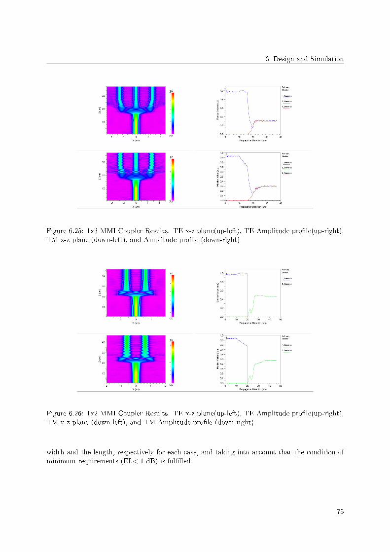
6. Design and Simulation
Figure 6.25: 1x3 MMI Coupler Results. TE x-z plane(up-left), TE Amplitude pro�le(up-right),TM x-z plane (down-left), and Amplitude pro�le (down-right)
Figure 6.26: 1x2 MMI Coupler Results. TE x-z plane(up-left), TE Amplitude pro�le(up-right),TM x-z plane (down-left), and TM Amplitude pro�le (down-right)
width and the length, respectively for each case, and taking into account that the condition ofminimum requirements (EL< 1 dB) is ful�lled.
75
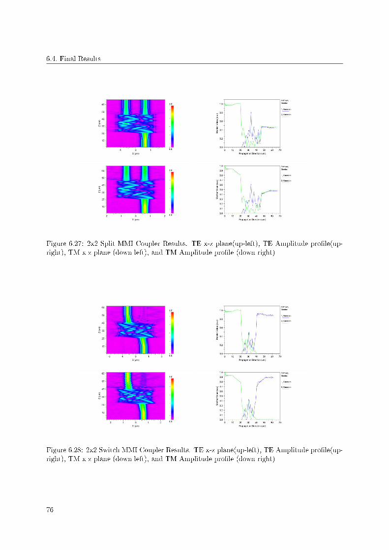
6.4. Final Results
Figure 6.27: 2x2 Split MMI Coupler Results. TE x-z plane(up-left), TE Amplitude pro�le(up-right), TM x-z plane (down-left), and TM Amplitude pro�le (down-right)
Figure 6.28: 2x2 Switch MMI Coupler Results. TE x-z plane(up-left), TE Amplitude pro�le(up-right), TM x-z plane (down-left), and TM Amplitude pro�le (down-right)
76

6. Design and Simulation
Input Output P1 P2 P3 Imbalance TM (dB) ELTM (dB)
1x3 0.303 0.298 0.302 0.072 0.4381x2 0.469 0.469 - 0 0.278
2x2switch 0.884 0.009 - - 0.4912x2split 0.485 0.47 - 0.136 0.199
Table 6.10: Imbalance and EL of a width tapered MMI Coupler. TM polarization. Final Result
Input Output PDL (dB)
1x3 0.1611x2 0.037
2x2switch 0.0932x2split 0.223
Table 6.11: PDL of the MMI Couplers. Final Result
Input Output FTwidthTE (nm) FTlength
TE (nm) FTwidthTM (nm) FTlength
TM (nm)
1x3 ± 46 ± 110 ± 17 ± 951x2 ± 100 ± 620 ± 150 ± 720
2x2switch ± 33 ± 374 ± 25 ± 3002x2split ± 18 ± 331 ± 39 ± 193
Table 6.12: Fabrication Tolerance of the MMI Couplers. Final Result
77

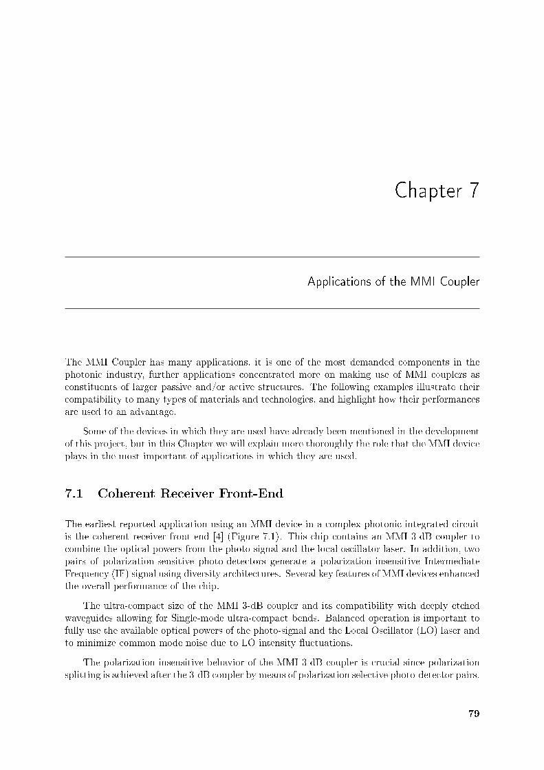
Chapter 7
Applications of the MMI Coupler
The MMI Coupler has many applications, it is one of the most demanded components in thephotonic industry, further applications concentrated more on making use of MMI couplers asconstituents of larger passive and/or active structures. The following examples illustrate theircompatibility to many types of materials and technologies, and highlight how their performancesare used to an advantage.
Some of the devices in which they are used have already been mentioned in the developmentof this project, but in this Chapter we will explain more thoroughly the role that the MMI deviceplays in the most important of applications in which they are used.
7.1 Coherent Receiver Front-End
The earliest reported application using an MMI device in a complex photonic integrated circuitis the coherent receiver front-end [4] (Figure 7.1). This chip contains an MMI 3-dB coupler tocombine the optical powers from the photo-signal and the local oscillator laser. In addition, twopairs of polarization-sensitive photo-detectors generate a polarization-insensitive IntermediateFrequency (IF) signal using diversity architectures. Several key features of MMI devices enhancedthe overall performance of the chip.
The ultra-compact size of the MMI 3-dB coupler and its compatibility with deeply etchedwaveguides allowing for Single-mode ultra-compact bends. Balanced operation is important tofully use the available optical powers of the photo-signal and the Local Oscillator (LO) laser andto minimize common mode noise due to LO intensity �uctuations.
The polarization insensitive behavior of the MMI 3-dB coupler is crucial since polarizationsplitting is achieved after the 3-dB coupler by means of polarization selective photo-detector pairs.
79

7.2. MZI
Figure 7.1: Coherent Receiver Front-end Schematic
This con�guration has the advantage, that in addition to being suitable for polarization-diversityreception, it is also suitable for phase-diversity detection. Finally, the wavelength insensitivebehavior of the 3-dB coupler in combination with the compact design of the photodetectorsshould result in a broad spectral operating range.
7.2 MZI
MZI [4] have been extensively used in practical realizations of optical processing because of theirnatural physical separation between the splitting/recombining functions and the phase-shiftingfunction.
Figure 7.2: Schematic Layouts of a MZI
80

7. Applications of the MMI Coupler
The extinction ratio in a MZI is directly limited by the imbalance of the input splitter andthe output combiner. For example, a 0.2-dB power imbalance would limit the extinction ratioto -33 dB. The good balancing and stable relative phases shown by MMI couplers around theiroptimum operating point, together with their polarization insensitivity make these devices idealcandidates for integration into Mach-Zehnder structures (Figure 7.2). MZI with MMI splittersand recombiners have also been experimented in hollow dielectric waveguides.
The MMI couplers plays a crucial role in attaining large bandwidth and polarization in-dependent operation. The possibility of achieving 1xN and NxN splitter/combiners with MMIdevices allows the realization of very compact integrated multi-way optical switches.
7.3 Micro-ring Resonator
Microring resonators [35] have been used as a basic building block for optical signal processingapplications such as optical switches, �lters, modulators, and add-drop multiplexers. Almost allof the reported works on micro-ring resonator structures have used directional couplers as thecoupling element. In order to meet a variety of requirements for high-speed signal processing,the coupling coe�cient needs to be adjusted arbitrarily and the directional couplers can meetthis requirement. However, for applications requiring high quality factor Q of the resonators, forhigh speed operation, the separations between two waveguides in the directional coupler mustbe very small.As a result, high loss due to conversion loss of modes is occurred recently. Also,the directional coupler has a large size and small fabrication tolerance.
Figure 7.3: Structure of a Micro-ring Resonator
Therefore, MMI couplers are used in such structures (Figure 7.3) instead of directional cou-plers due to their advantages of compactness, ease of fabrication, large fabrication tolerance andease of cascaded integration A micro-ring resonator based on a 2x2 MMI coupler was demon-strated on SOI channel waveguides for the �rst time.
81

7.4. Ring Lasers
7.4 Ring Lasers
MMI devices have also proven to be successful out-coupling elements in ring lasers [4]. The out-coupling element has a crucial in�uence on the performance of the ring laser, since the out-couplerforms an integral part of the ring resonator.
The most commonly used out-coupling element is the Y-junction, which o�ers ease of design,but can only couple one of the counter-propagating beams out of the ring. Directional couplershave not proven to be a successful out-coupler, partly due to their incompatibility with high-contrast waveguides which are required to create low-loss small-radii bends. MMI devices on theother hand provide symmetric out-coupling, relaxed fabrication tolerances, ease of design andcompatibility with high-contrast waveguides. An additional MMI combiner has been used tocombine both counter-propagating beams in a single output waveguide, thereby increasing thee�ciency.
Comparing the performance of ring lasers employing MMI couplers to those using Y-junctions,or directional couplers, the stability of the splitting ratio of the out-coupler is found to be thekey factor. Lasers are subject to varying operating conditions; changes in current a�ect the gainspectrum, change the temperature and cause carrier induced refractive index changes. If thesplitting ratio of the out-coupler, in turn, depends on wavelength, refractive index or excitationconditions, unstable lasing operation results, since laser performance is determined by the inter-play of all these parameters. It is therefore the extreme stability of the splitting ratio of the MMIcoupler, that leads to the improved performance of ring lasers incorporating MMI couplers.
82

Chapter 8
Conclusions and Future Prospects
Through the development of this project, we have reviewed the MultiMode Interference Coupler.The structure of this passive device is based on the MultiMode waveguide, and there for thetheory that backs these structures was fully outlined. In addition, the self-imagining principleand its properties, are the functioning principals in which all MMI devices are grounded on.
It was proposed to design a MMI Coupler on a SOI platform, which lead to investigate itstheoretical background, and to research about the several simulation tools based on numericalanalysis, so the testing of the design would be accurate and reliable. The answer was the use ofthe most commercial photonic simulator developed to analyze general dielectric waveguides, theBeamPROP, which included the e�ects of both guided and radiating �elds.
Through the use of this BPM based mode solver we performed simulations which permitted,not only the design but the optimization of the device, by determining the cause for the polariza-tion dependence, the power loss and the imbalance of the outputs. The results where 4 couplers(1x3, 1x2, 2x2split, and 2x2switch) with a exponentially and parabolically,depending on the case,width tapered MMI section (when necessary) and linearly tapered access waveguide, that wouldeliminate, or lower the gravity of the mentioned problems, enhancing their performance.
To corroborate these attributes the fabrication tolerance of the width and length of the TEand TM polarizations, respectively, has been shown together with other parameters like the PDLand the EL, not only proving the success of the project, but demonstrating its advantages andand qualities compared with other similar devices, so that it is clear that the MMI coupler thebest option in several optical circuit applications.
83

Bibliography
[1] A. Snyder and J. Love, Optical Waveguide Theory. Science Paperbacks, Chapman and Hall,1983.
[2] R. Syms and J. Cozens, Optical Guided Waves and Devices. McGraw-Hill, 1992.
[3] K. Okamoto, Fundamentals of Optical Waveguides. Elsevier Science, 2005.
[4] L. B. Soldano and E. C. M. Pennings, �Optical multi-mode interference devices based on self-imaging: Principles and applications,� tech. rep., Journal of Lightwave Technology, April1995.
[5] G. Reed and A. Knights, Silicon photonics: an introduction. John Wiley & Sons, 2004.
[6] �Silicon on insulator.� en.wikipedia.org/wiki/Silicon_on_insulator.
[7] �Photolithography.� en.wikipedia.org/wiki/Photolithography.
[8] �Etching.� en.wikipedia.org/wiki/Etching_microfabrication.
[9] P. Rai-Choudhury, Handbook of Microlithography, Micromachining, and Microfabrication.No. v. 1 in IEE materials & devices series, SPIE Optical Engineering Press, 1997.
[10] �Electron beam lithography.� en.wikipedia.org/wiki/Electron_beam_lithography.
[11] �Ion beam.� en.wikipedia.org/wiki/Ion_beam.
[12] K. S. Chiang and Q. Liu, �Formulae for the design of polarization-insensitive multimodeinterference couplers,� tech. rep., IEEE Photonic Technology Letters, September 2011.
[13] �Photonics.� en.wikipedia.org/wiki/Photonics.
[14] M. Lipson, �Guiding, modulating, and emitting light on silicon - challenges and opportuni-ties,� tech. rep., Journal of Lightwave Technology, December 2005.
85
Bibliography
[15] �Silicon photonics.� en.wikipedia.org/wiki/Silicon_photonics.
[16] �Refractive index.� en.wikipedia.org/wiki/Refractive_index.
[17] D. Krevelen and K. Te Nijenhuis, Properties of Polymers: Their Correlation With Chemical
Structure; Their Numerical Estimation and Prediction from Additive Group Contributions.Elsevier, 2009.
[18] B. E. Little and W. P. Huang, �Coupled mode theory for optical waveguides,� tech. rep.,Progress in Electromagnetics Research, 1995.
[19] A. Yariv, �Coupled mode theory for guided wave optics,� tech. rep., IEEE Journal of Quan-tum Electronics, September 1973.
[20] P. Humphreys, Extending Ourselves: Computational Science, Empiricism, and Scienti�c
Method. Oxford scholarship online, Oxford University Press, USA, 2004.
[21] S. Obayya, Computational Photonics. Wiley, 2011.
[22] Numerical Methods. McGraw-Hill Education (India) Pvt Ltd, 1999.
[23] �Numerical analysis.� en.wikipedia.org/wiki/Numerical_analysis.
[24] �Optical waveguide modeling.� http://optical-waveguides-modeling.net.
[25] F. Fernandez and Y. Lu, Microwave and optical waveguide analysis by the �nite element
method. Research Studies Press: Taunton, Somerset., 1996.
[26] J. Lin, �Theoretical investigation of polarization-insensitive multimode interference splitterson silicon-on-insulator,� tech. rep., IEEE Photonic Technology Letters, July 2008.
[27] T. T. Le and L. W. Cahill, �The design of multimode interference couplers with arbitrarypower splitting ratios on an soi platform,� tech. rep., Department of Electronic Engineering,La Trobe University, 2008.
[28] T. D. o. E. Fujisawa and S. K. M. Inf. Eng., Hokkaido Univ., �Full-vector �nite-elementbeam propagation method for three-dimensional nonlinear optical waveguides,� tech. rep.,Journal of Lightwave Technology, October 2002.
[29] �Rsoft design.� http://www.rsoftdesign.com.
[30] P. J. Olver, Introduction to Partial Di�erential Equations. 2012.
[31] A. Ta�ove and S. Hagness, Computational Electrodynamics: The Finite-Di�erence Time-
Domain Method. Artech House Antennas and Propagation Library, Artech House, 2005.
[32] M. T. Hill and M. K. Smit, �Optimizing imbalance and loss in 2x2 3-db multimode inter-ference couplers via access waveguide width,� tech. rep., Journal of Lightwave Technology,October 2003.
[33] D. Dai and S. He, �Optimization of ultracompact polarization-insensitive multimode inter-ference couplers based on si nanowire waveguides,� tech. rep., IEEE Photonic TechnologyLetters, October 2006.
86

Bibliography
[34] M. B. Lucas B. Soldano and M. K. Smit, �Large optical bandwidth of ingaasp/inp multi-mode interference 3-db couplers,� tech. rep., Delft University of Technology, Faculty ofElectrical Engineering and the Swiss Federal Institute of Technology.
[35] T. T. Le and L. W. Cahill, �The design of 4x4 multimode interference coupler based micror-ing resonator on an soi platform,� tech. rep., Journal of Telecommunications and InformationTechnology, 2010.
87


![SILICON MULTIMODE PHOTONIC INTEGRATED DE- VICES FOR …jpier.org/PIER/pier143/38.13111003.pdf · photonic multiplexing technologies [3], including wavelength-division-multiplexing](https://img.dokumen.tips/doc/110x75/5ecb1c5092fee2156248d38c/silicon-multimode-photonic-integrated-de-vices-for-jpierorgpierpier14338-.jpg)