Embed Size (px)
Citation preview

UNIVERSITA’ DEGLI STUDI DI PAVIA FACOLTA’ DI INGEGNERIA
DOTTORATO DI RICERCA IN
INGEGNERIA ELETTRONICA, INFORMATICA ED ELETTRICA
XIX CICLO
Design of mixed analog/digital interface circuits for sensors
and micro-systems
Relatore: Chiar.mo Prof Piero Malcovati
Tesi di dottorato di Andrea Rossini
Anno accademico 2005-2006


A mio papà Domenico e a mia mamma Tilde…
…una sola parola: grazie per tutto


4
Index Index............................................................................................... 4
Abstract .......................................................................................... 7 Chapter 1 Introduction ............................................. 9
Introduction................................................................................................................ 9 The light ................................................................................................................... 12 Gamma rays ............................................................................................................. 16 X rays ....................................................................................................................... 18
Photographic plate.....................................................................................................................20 Photostimulable Phosphors (PSPs) ...........................................................................................20 Geiger counter ...........................................................................................................................20 Scintillators ................................................................................................................................21 Image Intensification..................................................................................................................21 Direct Semiconductor Detectors................................................................................................21
Radio astronomy ...................................................................................................... 22 The acquisition chain ............................................................................................... 22 Design overview ...................................................................................................... 23
Chapter 2 The Read-Out Integrated Circuit ............... 25
Introduction.............................................................................................................. 25 The LFDR project .................................................................................................... 29 The ROIC chip ......................................................................................................... 31
The analog acquisition chain.....................................................................................................32 The digital processing chain ......................................................................................................34 The pipeline converter ...............................................................................................................35 The Wilkinson converter ............................................................................................................36
Layout of the test chip.............................................................................................. 37 Chapter 3 The Wilkinson A/D Converter .................. 41
Introduction.............................................................................................................. 41 The basic blocks....................................................................................................... 43
Ramp generator..........................................................................................................................43 Voltage Comparator ..................................................................................................................44 The clock generator ...................................................................................................................47 The counter and the output register...........................................................................................47
Measurement Setup.................................................................................................. 47 Experimental results................................................................................................. 49 Conclusions.............................................................................................................. 54
Chapter 4 Clock-less Pipeline-Like A/D Converter.... 56
Introduction.............................................................................................................. 56 Error on the gain of the amplifier..............................................................................................57 Error on the DAC level ..............................................................................................................59

5
Error in the comparator threshold ............................................................................................59 Basic blocks ............................................................................................................. 63
The ADC.....................................................................................................................................64 The residue amplifier .................................................................................................................65 The DAC.....................................................................................................................................68 The EOC generator....................................................................................................................69
Simulation Results ................................................................................................... 70 Experimental results................................................................................................. 76 Conclusions.............................................................................................................. 79
Chapter 5 Magnetic Sensor Models .......................... 81 Introduction.............................................................................................................. 81 Types of magnetic sensors ....................................................................................... 82
Squid ..........................................................................................................................................83 Search-coil .................................................................................................................................83 Magneto-inductive sensor ..........................................................................................................83 Magneto-resistance....................................................................................................................84 Hall sensor .................................................................................................................................88 Fluxgate .....................................................................................................................................90
The magnetic sensor model ..................................................................................... 94 Magneto-resistance....................................................................................................................96 Fluxgate .....................................................................................................................................97 Hall sensor .................................................................................................................................98 Magneto-inductance...................................................................................................................99 Temperature drift .....................................................................................................................101 Parasitic effects........................................................................................................................102 Dispersed field .........................................................................................................................103 Hysteresis .................................................................................................................................104
Experimental results............................................................................................... 106 Conclusions............................................................................................................ 109
Chapter 6 Interface Circuit for Fluxgate Magnetic
Sensor ................................................................................. 112 The interface circuit design.................................................................................... 112
Timing Block ............................................................................................................................114 Excitation Block .......................................................................................................................115 Read-Out Block ........................................................................................................................117 The ADC...................................................................................................................................118
Simulation Results ................................................................................................. 118 Layout .................................................................................................................... 121 Experimental results............................................................................................... 122 Conclusions............................................................................................................ 126
Bibliography............................................................................... 129
Acknowledgments/Ringraziamenti ............................................ 134

6

Ph.D thesis, Andrea Rossini 7
Abstract Scope of the work described in this thesis is the design of integrated interface circuits for microsensors.
This work can be divided into two parts. The first part describes the interface circuit for an array of X-
ray detectors, which is part of the acquisition chain for an X-ray spectrometer, that will be one of the
instruments used for the space mission towards Mercury “Bepi Columbus” of the European Space
Agency (ESA). More specifically a 10 bit clock-less pipeline-like A/D converter and a 10 bit
Wilkinson A/D converter have been designed, implemented and characterized. Moreover, we
implemented the complete interface circuit for a 16x16 array of X-ray detectors based on the Wilkinson
A/D converter. The complete acquisition chain achieves ±0.2 LSB of differential non-linearity, ±3.3
LSB of integral non-linearity and 34 electrons rms of input referred noise, consuming less than 1 mW
per channel.
The second part of the thesis deals with the interface circuit for an integrated fluxgate magnetic sensor
for electronic compass applications. The circuit can provide a widely programmable excitation current
to the fluxgate sensor and read-out the sensor signal, providing digital output. The interface circuit,
together with an integrated fluxgate sensor, achieves an angular error in detecting the Earth magnetic
field as low as 4 degrees.
This thesis is structured in the following way:
Chapter 1 Introduction
This chapter provides an overview of the integrated interface circuits for microsensors as well
as all the background information about X-ray detectors and detection systems.
Chapter 2 The Read Out Integrated Circuit
This chapter describes an interface circuit for an array of X-ray detectors. The project, named
Large Format Detector Readout, is funded by ESA (European Space Agency) and is carried-out
by University of Pavia, Polytechnic of Milano and Alcatel Alenia Space LABEN.
Chapter 3 The Wilkinson A/D converter

Ph.D thesis, Andrea Rossini 8
This chapter describes the first solution for implementing the A/D conversion in the read-out
integrated circuit described in Chapter 2: a 10-bit Wilkinson A/D converter. All the design and
implementation details are presented together with experimental results.
Chapter 4 Clock-less Pipeline- like A/D converter
This chapter describes the second solution for implementing the A/D conversion in the read-out
integrated circuit described in Chapter 2: a 10-bit clock-less pipeline-like A/D converter. The
peculiarity of this converter is the absence of the clock. The circuit, indeed, acts as a
combinatory logic, thus avoiding the presence of a synchronization. All the design and
implementation details are presented together with experimental results.
Chapter 5 Magnetic sensor models
This chapter provides the background information about magnetic sensors. Moreover, it
describes the magnetic sensors model that have been developed to simulate the behaviour of
four different types of sensors: an hall devices, a magneto-resistance, a flux-gate and a magneto-
inductance. These models have been used to design the interface circuit for fluxgate magnetic
sensors described in Chapter 6.
Chapter 6 Interface circuit for fluxgate magnetic sensor
This chapter describes the interface circuit for fluxgate magnetic sensors. The circuit can
provide a widely programmable excitation current to the fluxgate sensor and read-out the sensor
signal with variable gain. Moreover, the circuit provides digital output. All the design and
implementation details are presented together with experimental results.

Chapter 1 Interface circuits
Ph.D thesis, Andrea Rossini 9
Chapter 1
Introduction
1.1 Introduction
Computers can only handle zeros and ones and if we want to automate the procedure for sensing
any physical quantity in a repetitive mode, we need sensors to translate temperature, pressure,
vehicle speed or any other parameter into a form manageable by computers. This can be done with
appropriate interface circuits that translate the analog output of the sensors into the digital domain
of the computer.
Over the years, sensors have been fabricated by using many different technologies. At the
beginning, sensors were realized in a mechanical way, but, because of the success of the integrated
silicon technologies, also the sensor technology received renewed interest. Around 1965, Prof.
James Angell started a silicon sensor research group at Stanford University. One of his students,
Kensall Wise, started performing selective etching of structures and this marks the start of the
electronic sensors and the interface circuits as we know today. Many internationally well-known
universities in the USA, Europe and Japan were quick to follow.
Obviously, first applications of this sensors were bulky, costly and consuming a lot of power. But
following the development of the integrated circuit technology, new markets for these sensors were
found and even more new applications developed, thus increasing the effort to obtain even better
and cheaper sensors.
The main advantages of an electronic sensor are the lack of any mechanical part that can break, the
possibility to obtain a large number of pieces at the same price and with the same characteristics,
and, more importantly, the possibility to miniaturize the component itself step by step with the
evolution of the electronic integrated technologies.
Thus the need for sensors has grown rapidly in recent years for industrial control, automation and
consumer applications. In modern measurement and control systems, a large number of sensors
collect the information about the process variable in the system being monitored. They usually
provide analog information on the system being monitored through signal conditioning circuits
connected to a processor. The latter interprets the information, makes appropriate decisions most

Chapter 1 Interface circuits
Ph.D thesis, Andrea Rossini 10
likely in conjunction with higher-level control, and implements those decisions via actuators or it
displays the information to the human world.
When developing an interface circuit for sensors, the designer has to take into account several
aspects about not only the electronics itself, but also about the system and the sensor characteristics
as well as the environment where the sensor has to work.[1]
The first step in any sensing device design is to define what is to be sensed and how. The
identification of the physical parameter (quantity) to be sensed is not always obvious. An example
to build a flow meter consists in measuring the rotation of an impeller blade. In this case, it would
be easy to assume that what is to be sensed is the rotation of the impeller blade. In fact, fluid flow is
the desired quantity to be sensed. The limiting identification of the impeller blade motion as the
parameter to be sensed, reduces the possible design approaches and available technologies open to
the designer. In most cases, several methods of sensing a physical parameter can be identified. Each
of these methods will consist of a conceptual approach with an associated technology. The
conceptual approach describes how the sensing function might be implemented without considering
the engineering details and component specifications. At this level of detail, some conceptual
approaches can be immediately eliminated on the basis of cost, complexity, etc. Physical parameters
can often be sensed by using indirect methods: as an example, the requirement to sense temperature
changes. An obvious approach would be to use a thermocouple since it is a temperature sensor. An
alternative method can be a magnetic sensor glued over a bellows. An increase and/or decrease in
temperature causes the bellows to expand or contract, moving the attached magnet. The
corresponding change in magnetic field is sensed by a magnetic sensor, for instance a Hall device.
The final result turns out to be the conversion of the input temperature into a measurable electrical
field or into a current/voltage.
Once the most promising sensing techniques are identified, it is necessary to determine input and
output requirements, the major sensing device components, and the application requirements. For
example, which are the electrical characteristics of the output pulse required for the application
(current, voltage, rise time, fall time, etc.) and if the sensors are able to fulfil it. If the required
electrical characteristics are not met at the output of the sensors, it is necessary to find which
additional circuitry is required. The environmental requirements must also be identified. For
example, if a sensing device has to be used in oil laden air maybe to sense the level of oil in a car,
then an optical approach would be discarded. The strengths and weaknesses of each approach must
be weighed. The features and benefits of each technology must be evaluated with respect to the

Chapter 1 Interface circuits
Ph.D thesis, Andrea Rossini 11
considered application. During the preliminary feasibility study, it is important that all the key
informations are considered. Among them, we can mention:
• the overall cost;
• the volume productivity;
• the component availability;
• the sensor complexity;
• the tolerance of part-to-part variations;
• the compatibility with other system components;
• the reliability;
• the repeatability;
• the maintainability;
• the environmental constraints.
Although several of these considerations can not be quantified until a detailed design is completed,
they must, nevertheless, be weighed at this point.
An important consideration about the interface circuit and the sensor itself when exploiting the
possibility to use integrated circuits is the possibility to integrate both the interface circuit and
several sensors on the same chip or in the same package, leading to micro-systems or micro-
modules[2]. The potential advantages of this approach are: the cost of the measurement system is
strongly reduced thanks to batch fabrication of both sensors and interface circuits, its size and
interconnections are minimized, and its reliability is improved. However, the choice of materials
compatible with silicon IC technologies is limited and their properties are process-dependent.
Therefore, integrated sensors often show worse performance than their discrete counterparts due to
weak signals, offset and nonlinear transfer characteristics. This explains the increasing demand for
sensors interface. There are two possible approaches for implementing micro-sensor systems: the
micro-system approach and the micro-module approach. In the micro-system approach, the sensor
and the interface circuitry are integrated on the same chip. Therefore, a micro-sensor must be
designed by taking into account the material characteristics given by the standard IC process used.
Furthermore, it has to be considered that, when the standard IC fabrication flow is completed,
additional specific process steps are required in order to implement the sensor itself By exploiting
this approach it is worth to point out that cost and yield issues can rise, especially when using
modern technologies with small feature size. In fact, while the silicon area occupied by the interface

Chapter 1 Interface circuits
Ph.D thesis, Andrea Rossini 12
circuit is typically shrinking, together with the feature size of the technology, the sensor area in
most cases remains constant. Therefore, while for integrated circuits the increasing cost per unit
area is abundantly compensated by the reduction in silicon area, leading to an overall reduction of
chip cost with the technology feature size, this might not be true for integrated micro-systems.
Moreover, a defect in the sensors may force us to discard the complete micro-system, even if the
circuitry is working, thereby lowering the yield and again increasing the overall cost. It has to be
underline that parasitic elements due to the interconnections between the sensor and the interface
circuitry are minimized and, more importantly, are well-defined and reproducible. In addition, the
system assembly is simple, inexpensive, and independent of the number of connections needed,
since all the interconnections are implemented during the IC fabrication process. Finally, when
required, the use of the same technology allows us achieving good matching performances between
elements of the sensor and of the interface circuitry. This way accurate compensation of many
parasitic effects can be obtained.
In the micro-module approach, the sensors and the interface circuitry are integrated in different
chips. They are included in the same package or mounted on the same substrate, The
interconnections between the sensor chip and the interface circuit chip can be realized with bonding
wires or other techniques. The two chips can be fabricated with two different technologies, which
are optimized for the sensors and the circuitry. The sensor designer can adjust the material
properties of the technology to optimize the performance of the device, and cost and yield issues
mentioned for the micro-system approach are no longer a concern. However, also the micro-module
approach has a number of drawbacks. First, the assembling of the system can be quite expensive
and a source of possible failures, the number of interconnections allowed between the sensor and
the circuitry is limited. Moreover, the parasitic elements due to the interconnections are some orders
of magnitude larger, more unpredictable, and less repeatable than in the micro system approach,
thus limiting in many cases the effectiveness of any improvements obtained in sensor performance
by technology optimization. Finally, matching between elements of the sensor and of the interface
circuitry cannot be guaranteed. The advantages and disadvantages of both approaches are
summarized in Table 1.1-1.

Chapter 1 Interface circuits
Ph.D thesis, Andrea Rossini 13
Table 1.1-1: Micro-system versus micro-module approach
In the next chapters we will present two interface circuits for sensors, designed for different
applications. One is for a X-ray spectrometer, while the second is for an electronic compass. In the
following paragraphs we will provide some background information on X-ray detectors, while the
state of the art on magnetic sensors is described in chapter 6.
1.2 The light
The only thing that can flow between planets is light. The light is a kind of electromagnetic
radiation, but it is not the only one. In particular, the light as we know is part of the spectrum, that
means the range of all possible electromagnetic radiations that exist in the universe. The visible
spectrum is the portion of the electromagnetic spectrum that is visible to the human eye.
Electromagnetic radiation in this range of wavelengths is called visible light or simply light. There
are no exact bounds to the visible spectrum; a typical human eye will respond to wavelengths from
400 nm to 700 nm. From Figure 1.2-1 it is possible to realize that light as we know it is only a small
part of the total radiation available. If we were able to see all the spectrum we could have more and
more information about all the space around us, but not only, they can give us the tools to built new
applications and open new worlds. The effect of research in this field are various, some simple
applications like television, mobile phone, medical device for radiography, can give and idea how
knowledge over this field is important . This is what scientists correctly though at the beginnings
and explain why research in this field is so much important.
Micro-system Approach Micro-module Approach
+ Reliability + Optimal yield
+ Minimal interconnection parasitic + Optimal process both for sensor and
circuitry
+ Simple and inexpensive assembly + Cost that scales with feature size
- Reduced yield - Reliability
- Cost that doesn’t scales with feature size - Large interconnection parasitic
- Optimal process only for sensor - Expensive assembly

Chapter 1 Interface circuits
Ph.D thesis, Andrea Rossini 14
Nearly all objects in the universe emit, reflect and/or transmit some light. The distribution of this
light along the electromagnetic spectrum (called the spectrum of the object) is determined by the
object composition. Several types of spectra can be distinguished depending upon the nature of the
radiation coming from an object:
• if the spectrum is composed primarily of thermal radiation emitted by the object itself, an
emission spectrum occurs;
• some bodies emit more or less light according to the blackbody spectrum;
• if the spectrum is composed of background light, and the object is able to transmit some part
of it or to absorb it, then an absorption spectrum occurs.
The light is thus composed by different radiations, gamma ray, X-ray ultra-violet, infrared,
microwaves and radiowaves, as shown in Figure 1.2-1.
Figure 1.2-1: Electromagnetic radiation spectrum
Radiowaves generally are used by antennas of appropriate size (according to the principle of
resonance), with wavelengths ranging from hundreds of meters to about hundreds of millimetres.
They are used for data transmission. Television, mobile phones, wireless networking and amateur
radio all use radiowaves.
The super high frequency (SHF) and extremely high frequency (EHF) of Microwaves come next up
the frequency scale. Microwaves are waves which are typically short enough to employ tubular
metal waveguides of reasonable diameter. Microwave energy is produced with klystron and
magnetron tubes, and with solid state diodes such as Gunn and IMPATT devices. Microwaves are
absorbed by molecules that have a dipole moment in liquids. In a microwave oven, this effect is
used to heat food. Low-intensity microwave radiation is used in Wi-Fi internet connection.
Terahertz radiation is a region of the spectrum between far infrared and microwaves. Until now, the
range has been rarely studied and few sources existed for microwave energy at the high end of the

Chapter 1 Interface circuits
Ph.D thesis, Andrea Rossini 15
band (sub-millimetre waves or so-called terahertz waves), but applications such as imaging and
communications are now appearing. Scientists are also looking to apply Terahertz technology in the
armed forces, where high frequency waves might be directed at enemy troops to incapacitate their
electronic equipments.
The infrared part of the electromagnetic spectrum covers the range from roughly 300 GHz (1 mm)
to 400 THz (750 nm). It can be divided into three parts:
• Far-infrared, from 300 GHz (1 mm) to 30 THz (10 μm). The lower part of this range may
also be called microwaves. This radiation is typically absorbed by so-called rotational
modes in gas-phase molecules, by molecular motions in liquids, and by phonons in
solids. The water in the Earth's atmosphere absorbs so strongly in this range that it
renders the atmosphere effectively opaque. However, there are certain wavelength
ranges ("windows") within the opaque range which allow partial transmission, and can
be used for astronomy. The wavelength range from approximately 200 μm up to a few
mm is often referred to as "sub-millimetre" in astronomy, reserving far infrared for
wavelengths below 200 μm.
• Mid-infrared, from 30 to 120 THz (10 to 2.5 μm). Hot objects (black-body radiators) can
radiate strongly in this range. It is absorbed by molecular vibrations, i.e. when different
atoms in a molecule vibrate around their equilibrium positions. This range is sometimes
called the fingerprint region since the mid-infrared absorption spectrum of a compound
is very specific for that compound.
• Near-infrared, from 120 to 400 THz (2500 nm to 750 nm). Physical processes that are
relevant for this range are similar to those for visible light.
By moving to higher frequencies (Figure 1.2-1) the ultraviolet region can be found. The wavelength
of the radiation in this zone is shorter than the violet end of the visible spectrum.
Being very energetic, UV can break chemical bonds, making molecules unusually reactive or
ionizing them, in general changing their mutual behaviour. Sunburn, for example, is caused by the
disruptive effects of UV radiation on skin cells, which can even cause skin cancer, if the radiation
damages the complex DNA molecules in the cells (UV radiation is a proven mutagen). The Sun
emits a large amount of UV radiations, which could quickly turn Earth into a barren desert, but
most of them are absorbed by the atmosphere ozone layer before reaching the planet surface.

Chapter 1 Interface circuits
Ph.D thesis, Andrea Rossini 16
After UV we have the X-rays. Hard X-rays have shorter wavelengths than soft X-rays. Sources of
X-rays are stars, and strongly some types of nebulae, Neutron stars and accretion disks around black
holes. X-rays are used for they ability to pass through many substances, and this feature makes them
useful in medicine and industry fields. An X-ray machine works by firing a beam of electrons at a
"target". If the electron beam intensity is adequate, X-rays can be produced.
In Figure 1.2-1, hard X-rays are followed by gamma rays. These are the most energetic photons,
having no lower limits to their wavelength. They are useful to astronomers in the study of high-
energy objects or regions and they are used by physicists, thanks to their penetrative ability and
thanks to the possibility to be produced from radioisotopes. The wavelength of gamma rays can be
measured with high accuracy by means of Compton scattering.
Note that there are no defined boundaries between the types of electromagnetic radiations. Some
wavelength is characterized by properties typical of two regions of the spectrum. For example, red
light resembles infra-red radiation since it can be able to resonate some chemical bonds. At the
same times there is an overlap between the hard X-rays and the gamma rays that doesn’t permit to
define a sharp limit between the two radiation.
Since this two last form of radiation are the highest-energy end of the electromagnetic spectrum, we
will focus our attention on their nature, their possible applications and how to detect them.
1.3 Gamma rays
As explained in the previous paragraph, gamma rays form the highest-energy end of the
electromagnetic spectrum. They are often defined to begin at an energy of 10 keV, corresponding to
a minimum frequency of 2.42 EHz (ExaHertz or 1018 Hertz), or a maximum wavelength of 124 pm,
although electromagnetic radiation from around 10 keV to several hundred keV is also referred to
as hard X-rays. It is important to note that there is no physical difference between gamma rays and
X-rays of the same energy. They are two names for the same electromagnetic radiation, just like
sunlight and moonlight are two names for visible light. Rather, gamma rays are distinguished from
X-rays by their origin. Gamma ray is a term for high-energy electromagnetic radiation produced by
nuclear transitions, while X-ray is a term for high-energy electromagnetic radiation produced by
energy transitions due to accelerating electrons. Since it is possible for some electron transition to
be of higher energy than some nuclear transitions, there is an overlap region between what it is
referred to as low energy gamma rays and high energy X-rays.

Chapter 1 Interface circuits
Ph.D thesis, Andrea Rossini 17
Gamma rays are a form of ionizing radiation; they are more penetrating than either alpha or beta
radiation (neither of which is electromagnetic radiation), but less ionizing. For instance, a gamma
ray will pass through 1 cm of aluminium, while an alpha particle will be stopped by even a single
sheet of paper. Gamma sources are used for a number of applications in both medicine and industry
field.
When a gamma ray passes through matter, its probability of absorption is proportional to the
thickness of the layer itself. In passing through matter, gamma radiation ionizes via three main
processes: the photoelectric effect, Compton scattering, and pair production, [3], [4], [5].
• Photoelectric Effect: This describes the case in which a gamma photon interacts with atoms
and transfers its energy to an atomic electron, ejecting that electron from the atom. The
kinetic energy of the resulting photoelectron is equal to the energy of the incident
gamma photon minus the binding energy of the electron. The photoelectric effect is the
dominant energy transfer mechanism for X-ray and gamma ray photons with energies
below 50 keV, but it is much less important at higher energies.
• Compton Scattering: This is an interaction in which an incident gamma photon transfers
enough energy to an atomic electron to cause its ejection, with the remainder of the
original photon's energy being emitted as a new, lower energy gamma photon with an
emission direction different from that of the incident gamma photon. The probability of
Compton scatter decreases with increasing photon energy. Compton scattering is
considered to be the main absorption mechanism for gamma rays in the intermediate
energy range (100 keV to 10 MeV). It can be interesting to note that such an energy
spectrum includes most gamma radiations present in a nuclear explosion. Compton
scattering is relatively independent of the atomic number of the absorbing material.
• Pair Production: By interaction via the Coulomb force, in the proximity of the nucleus, the
energy of the incident photon is spontaneously converted into the mass of an electron-
positron pair. A positron is the anti-matter equivalent of an electron; it has the same
mass as an electron, but it has a positive charge equal in strength to the negative charge
of an electron. Energy in excess of the equivalent rest mass of the two particles
(1.02 MeV) appears as the kinetic energy of the pair and the recoil nucleus. The positron
has a very short lifetime (about 10-8 seconds). The positron combines with a free
electron and the entire mass of these two particles is then converted into two gamma
photons of 0.51 MeV energy each.

Chapter 1 Interface circuits
Ph.D thesis, Andrea Rossini 18
The secondary electrons (or positrons) produced in any of these three processes frequently have
enough energy to produce many ionizations up to the end of range.
The nature of gamma rays makes them useful to kill bacteria in medical equipments sterilization
process. They are also used to kill insects in foodstuffs, particularly meat, marshmallows, pies,
eggs, and vegetables.
Due to their tissue penetrating property, gamma rays and X-rays have a wide variety of medical
uses such as in CT (Computerised Tomography) Scans and radiation therapy. However, as a form
of ionizing radiation, they have the capability to produce molecular changes, particularly to DNA,
giving them the potential to cause cancer.
Despite their cancer-causing properties, gamma rays are also used to treat some types of cancer. In
the procedure called gamma-knife surgery, multiple concentrated beams of gamma rays are directed
on the growth in order to kill the cancerous cells. The beams are aimed from different angles to
focus the radiation on the growth while minimizing damages to the surrounding tissues.
Gamma rays are also used for diagnostic purposes in nuclear medicine. Several gamma-emitting
radioisotopes are used in such a field. One of these is technetium-99m. When administered to a
patient, a gamma camera can be used to form an image of the radioisotope distribution by detecting
the gamma radiation emitted. Such a technique can be employed to diagnose a wide range of
conditions (e.g. spread of cancer to the bones).
Gamma ray detectors are also starting to be used in Pakistan as part of the Container Security
Initiative (CSI). These machines are advertised to scan 30 containers per hour. The objective of this
technique is to pre-screen merchant ship containers before they enter ports.
1.4 X rays
X-rays are a form of electromagnetic radiation with a wavelength in the range from 10 to 0.01 nm,
corresponding to frequencies in the range from 30 to 30000 PHz (1015 Hertz). X-rays are primarily
used for diagnostic radiography and crystallography. X-rays are a form of ionizing radiation and as
such can be dangerous.
When medical X-rays are being produced, a thin metallic sheet is placed between the emitter and
the target, effectively filtering out the lower energy (soft) X-rays. The resultant X-ray is called hard.
Soft X-rays overlap the range of extreme ultraviolet. The frequency of hard X-rays is higher than
the one of soft X-rays, and the wavelength is shorter. Hard X-rays overlap the range of "long"-
Chapter 1 Interface circuits
Ph.D thesis, Andrea Rossini 19
wavelength (lower energy) gamma rays. However, the distinction between the two terms depends
on the source of the radiation, not on its wavelength. X-ray photons are generated by energetic
electron processes, while gamma rays by transitions within atomic nuclei.
The basic production of X-rays is obtained by accelerating electrons in order to collide with a metal
target (usually tungsten, but sometimes molybdenum). Here the electrons suddenly decelerate upon
colliding with the metal target and, if the electron is energetic enough, it is able to knock out an
electron from the inner shell of the metal atom. As a result, electrons from higher energy levels fill
up the vacancy and X-ray photons are emitted. This causes the spectral line part of the wavelength
distribution. There is also a continuum bremsstrahlung component given off by the electrons as they
are scattered by the strong electric field near the high Z (proton number) nuclei.
Nowadays, for many (non medical) applications, X-ray production is achieved by synchrotrons.
The detection of X-rays is based on various methods. The most popular methods are a photographic
plate, X-ray film in a cassette, and rare earth screens.
1.4.1 Photographic plate
The X-ray photographic plate or film is used in hospitals to produce images of the internal organs
and bones of a patient. The part of the patient to be X-rayed is placed between the X-ray source and
the photographic receptor to produce what is a shadow of all the internal structures of that particular
part of the body being X-rayed. The X-rays are blocked by dense tissues such as bone and pass
through soft tissues. Those areas where the X-rays strike the photographic receptor turn black when
it is developed. So where the X-rays pass through "soft" parts of the body such as organs, muscles,
and skin, the plate or film turns out to be black. Contrast compounds containing barium or iodine,
which are radiopaque, can be injected in the artery of a particular organ, or given intravenously. The
contrast compounds essentially block the X-rays and, hence, the circulation of the organ can be
more readily seen. For some procedures, the contrast can have a syrupy consistency, which can be
thinned by warming, and is introduced with a power injector, such as the Nemoto Injector.

Chapter 1 Interface circuits
Ph.D thesis, Andrea Rossini 20
1.4.2 Photostimulable Phosphors (PSPs)
An increasingly common method of detecting X-rays is the use of Photostimulable Luminescence
(PSL), pioneered by Fuji in the 1980's. In modern hospitals a PSP plate is used instead of the
photographic plate. After the plate is X-rayed, excited electrons in the phosphor material remain
'trapped' in 'colour centres' in the crystal lattice until stimulated by a laser beam passed over the
plate surface. The light given off during laser stimulation is collected by a photomultiplier tube and
the resulting signal is converted into a digital image by computer technology, which gives this
process its common name, computed radiography. The PSP plate can be used over and over again.
1.4.3 Geiger counter
Initially, most common detection methods were based on the ionisation of gases, as in the Geiger-
Müller counter: a sealed volume, usually a cylinder, with a polymer or thin metal window contains
a gas, and a wire. An high voltage is applied between the cylinder (cathode) and the wire (anode).
When an X-ray photon enters the cylinder, it ionises the gas. These ions accelerate toward the
anode, in the process causing further ionisation along their trajectory. This process, known as an
avalanche, is detected as a sudden flow of current, called a "count" or "event". Finally, the electrons
form a virtual cathode around the anode wire drastically reducing the electric field in the outer
portions of the tube. This halts the collision ionizations and limits further growth of avalanches. As
a result, all "counts" on a Geiger counter are the same size and it can give no indication as to the
particle energy of the radiation, unlike the proportional counter. The intensity of the radiation is
measurable by the Geiger counter as the counting-rate of the system.
In order to gain energy spectrum information a diffracting crystal may be used to first separate the
different photons. The method is called wavelength dispersive X-ray spectroscopy (WDX or WDS).
Position-sensitive detectors are often used in conjunction with dispersive elements. Other inherently
energy-resolving detection equipments may be used, such as the aforementioned proportional
counters. In either case, the use of suitable pulse-processing (MCA) equipments allows digital
spectra to be created for later analysis.
For many applications, counters are not sealed but are constantly fed with purified gas (thus
reducing problems of contamination or gas aging). These are called "flow counter".
Chapter 1 Interface circuits
Ph.D thesis, Andrea Rossini 21
1.4.4 Scintillators
Some materials such as sodium iodide (NaI) can "convert" an X-ray photon to a visible photon; an
electronic detector can be built by adding a photomultiplier. These detectors are called
"scintillators", filmscreens or "scintillation counters". The main advantage of using these is that an
adequate image can be obtained while subjecting the patient to a much lower dose of X-rays.
1.4.5 Image Intensification
X-rays are also used in "real-time" procedures such as angiography or contrast studies of the hollow
organs (e.g. barium enema of the small or large intestine) using fluoroscopy acquired with an image
intensifier. Angioplasty, medical interventions of the arterial system, rely heavily on X-ray-sensitive
contrast to identify potentially treatable lesions.
1.4.6 Direct Semiconductor Detectors
Since 1970s, new semiconductor detectors have been developed (silicon or germanium doped with
lithium, Si(Li) or Ge(Li)). X-ray photons are converted to electron-hole pairs in the semiconductor
and are collected to detect the X-rays. When the temperature is low enough (the detector is cooled
by Peltier effect or better by liquid nitrogen), it is possible to directly determine the X-ray energy
spectrum. This method is called energy dispersive X-ray spectroscopy (EDX or EDS) and it is often
used in small X-ray fluorescence spectrometers. These detectors are sometimes called "solid
detectors". Cadmium telluride (CdTe) and its alloy with zinc, cadmium zinc telluride detectors have
an increased sensitivity, which allows lower doses of X-rays to be used. These kind of detectors
have not been adopted in practical applications in Medical Imaging until 1990's. Actually,
amorphous selenium is used in commercial large area flat panel X-ray detectors for chest
radiography and mammography. Silicon drift detectors (SDDs), produced by conventional
semiconductor fabrication process, now provide a cost-effective and high resolving radiation
measurement. They replace conventional X-ray detectors, such as Si(Li)s, since liquid nitrogen
cooling process is not required.

Chapter 1 Interface circuits
Ph.D thesis, Andrea Rossini 22
1.5 Radio astronomy
Radio astronomy is the field in which study of gamma and x-rays is most helpful. Radio astronomy
is the study of celestial phenomena through measurements of the characteristics of radio waves
emitted by physical processes occurring in the space. In order to receive good signals, radio
astronomy requires large antennas, or arrays of smaller antennas all working together (the Very
Large Array near Socorro, New Mexico can be taken such an example). Most radio telescopes use a
parabolic dish to reflect the waves to a receiver which, in turn, detects and amplifies the signal into
usable data. This allows astronomers to see a region of the radio sky. By taking multiple scans of
overlapping strips of the sky it is possible to reconstruct an image ('mosaicing'). Radio astronomy is
a relatively new field of astronomical research that still has much more to be discovered.
Radio astronomy has led to substantial increases in astronomical knowledge, particularly with the
discovery of several classes of new objects, including pulsars, quasars and radio galaxies. This has
been possible since radio astronomy allows detecting things that are not observable in optical
astronomy. Radio astronomy is also partly responsible of the idea that dark matter is an important
component of our universe. Radio measurements of the rotation of galaxies suggest that there is
much more mass in galaxies than the one which has been directly observed (see Vera Rubin). The
cosmic microwave background radiation was also first detected using radio telescopes. However,
radio telescopes have also been used to investigate objects much closer to our planet, including
observations of the Sun and solar activity, together with planets radar mapping.
Radio telescopes can now be found all over the world. Widely separated telescopes are often
combined using a technique called interferometry in order to obtain observations with much higher
resolution with respect the one that could be achieved by using a single receiver. Initially,
telescopes within a few kilometres of each other were combined (see, for example, the Mullard
Radio Astronomy Observatory), but since the 1970s telescopes from all over the world (and even in
Earth orbit) have been combined to perform Very Long Baseline Interferometry.
1.6 The acquisition chain
Once the X-rays or gamma rays are detected and the proportional electrical signal is available, it is
necessary to develop all the circuitry to process the signal itself. In a typical acquisition chain,
shown in Figure 1.6-1, the charge produced by the detector is similar to a current Dirac delta. This

Chapter 1 Interface circuits
Ph.D thesis, Andrea Rossini 23
charge is integrated in a charge sensitive amplifier (CSA), that produces a voltage step at the output
equal to the charge divided by the feedback capacitor. This voltage step is filtered by means of a
band-pass filter (or pulse shaper amplifier, PSA) in order to reduce the noise and increase the
signal-to-noise ratio (SNR). The resulting output is a waveform whose peak value is related to the
area of the detector current pulse and, hence, to the energy absorbed. The peak of the signal
typically occurs after few microseconds (depending on the characteristics of the filter). The useful
information for the data processing is therefore contained in the peak value of the signal obtained at
the output of PSA. In order to digitize this value, the analog chain requires a specific circuit that
detects the peak and then stores it for the A/D conversion,[6] ,[7].
Figure 1.6-1: The acquisition chain
1.7 Design overview
In the next chapters we will describe an interface circuit for X-rays spectrometry called “Read-Out
Integrated Circuit” (ROIC). The circuit has been developed in the frame of a project of the
European Space Agency (ESA) named LFDR, Large Format Detector Read-out, for the detection of
X-rays emitted by the Sun and reflected by the surface of Mercury. This project is scheduled to be
used in the ‘Bepi Colombo’ space ship. The Mercury mission, proposed in May 1993 and accepted
by the Scientific Program Commission (SPC) in September 1999, takes its name form the Italian
scientist Giuseppe Colombo (1920-1984), first man to explain the peculiar rotation of Mercury, that
rotates three times on itself every two rotations around the Sun. The expect lift-off date is planned
for August 2009, while the land on the surface of Mercury is scheduled for October 2012. The
activity of design of the ASIC is a collaboration between the University of Pavia, Laben Alenia
Alcatel Spazio and Politecnico di Milano, [8].

Chapter 1 Interface circuits
Ph.D thesis, Andrea Rossini 24
Chapter 2 The Read-Out Integrated Circuit
Ph.D thesis, Andrea Rossini 25
Chapter 2 The Read-Out Integrated Circuit
In this chapter we describe an interface circuit for a matrix of X-rays sensors. The project,
named Large Format Detector Readout (LFDR), is founded by the European Space Agency
(ESA) in cooperation with University of Pavia, Politecnico di Milano and Laben Alcatel Alenia
Space.
2.1 Introduction
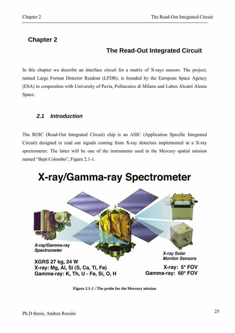
The ROIC (Read-Out Integrated Circuit) chip is an ASIC (Application Specific Integrated
Circuit) designed to read out signals coming from X-ray detectors implemented in a X-ray
spectrometer. The latter will be one of the instruments used in the Mercury spatial mission
named “Bepi Colombo”, Figure 2.1-1.
Figure 2.1-1 : The probe for the Mercury mission

Chapter 2 The Read-Out Integrated Circuit
Ph.D thesis, Andrea Rossini 26
The Mercury mission, proposed in May 1993 and accepted by the Scientific Program
Commission (SPC) in September 1999, takes its name form the Italian scientist Giuseppe
Colombo (1920-1984), first man to explain the peculiar rotation of Mercury, that rotates three
times on itself every two rotations around the Sun. The expected lift-off date is planned for
August 2009, while the land on the surface of Mercury is scheduled for October 2012.
The mass of the space ship at the take-off will be approximately 1500 kg while it is previewed
that at the arrival on the planet surface it will be about 1100 kg. Mercury is the nearest planet to
the Sun and its exploration should give important informations about the origins of the solar
system.
Mercury, Venus, Earth and Mars form the ‘terrestrial planet family’ and everyone carries
essential informations to reconstruct the history of this group. Knowing their origins and their
evolution is a milestone to know how the conditions necessary for life in our solar system have
been developed and if it is possible to find the same conditions in other systems. Moreover,
thanks to the proximity to the Sun, it will be possible to investigate the validity of the Einstein
gravity theory.
After one year of theoretical studies about the technologies and the system finished in 1999, the
best approach to reach the proposed goals is to send two Orbiters and one Lander:
• The Mercury Planetary Orbiter (MPO), shown in Figure 2.1-2, is a module that will
be in a low orbit at the nadir to observe and relieve the planet.
Figure 2.1-2: The Mercury Planetary Orbiter (MPO) module
Chapter 2 The Read-Out Integrated Circuit
Ph.D thesis, Andrea Rossini 27
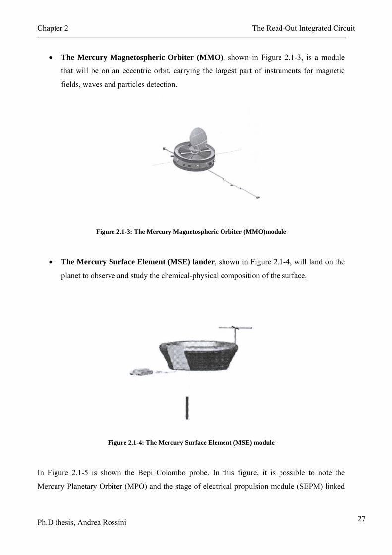
• The Mercury Magnetospheric Orbiter (MMO), shown in Figure 2.1-3, is a module
that will be on an eccentric orbit, carrying the largest part of instruments for magnetic
fields, waves and particles detection.
Figure 2.1-3: The Mercury Magnetospheric Orbiter (MMO)module
• The Mercury Surface Element (MSE) lander, shown in Figure 2.1-4, will land on the
planet to observe and study the chemical-physical composition of the surface.
Figure 2.1-4: The Mercury Surface Element (MSE) module
In Figure 2.1-5 is shown the Bepi Colombo probe. In this figure, it is possible to note the
Mercury Planetary Orbiter (MPO) and the stage of electrical propulsion module (SEPM) linked

Chapter 2 The Read-Out Integrated Circuit
Ph.D thesis, Andrea Rossini 28
with the Chemical Propulsion Module (CPM). In the background are depicted the Mercury
Magnetospheric Orbiter (MMO) and the Mercury Surface Element (MSE).
Figure 2.1-5: The Bepi Colombo probe
The interplanetary journey will use an electrical propulsion system fed by solar energy. This
module will be unfastened at the arrival on the planet surface. The Chemical Propulsion Module
(CPM) will be used for all the movements necessary to reach the established orbit. Finally, after
that all the elements are ready and out of the probe, including MSE, the CPM will be unfastened
as well.
The basic idea is to divide the ship elements in two structures that use propulsion engines really
similar. The ship is divided into modules and it is suitable for a large variety of choices
compatible with the objective of the mission.
Chapter 2 The Read-Out Integrated Circuit
Ph.D thesis, Andrea Rossini 29
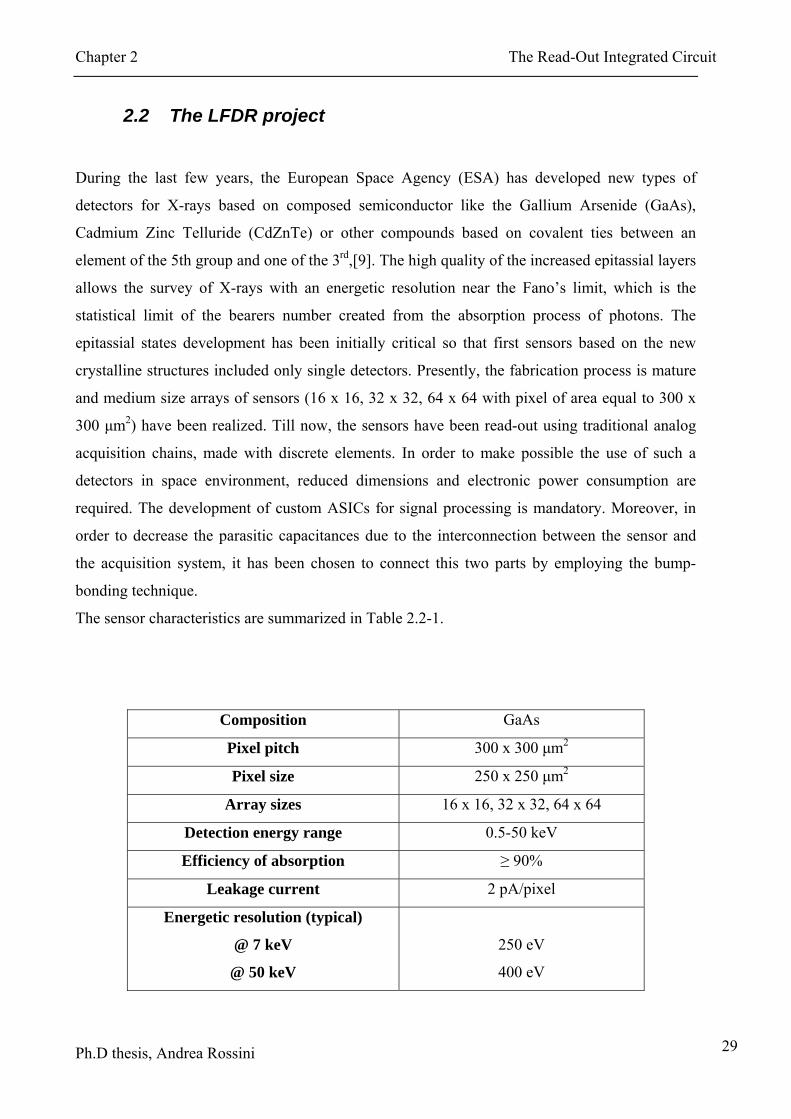
2.2 The LFDR project
During the last few years, the European Space Agency (ESA) has developed new types of
detectors for X-rays based on composed semiconductor like the Gallium Arsenide (GaAs),
Cadmium Zinc Telluride (CdZnTe) or other compounds based on covalent ties between an
element of the 5th group and one of the 3rd,[9]. The high quality of the increased epitassial layers
allows the survey of X-rays with an energetic resolution near the Fano’s limit, which is the
statistical limit of the bearers number created from the absorption process of photons. The
epitassial states development has been initially critical so that first sensors based on the new
crystalline structures included only single detectors. Presently, the fabrication process is mature
and medium size arrays of sensors (16 x 16, 32 x 32, 64 x 64 with pixel of area equal to 300 x
300 μm2) have been realized. Till now, the sensors have been read-out using traditional analog
acquisition chains, made with discrete elements. In order to make possible the use of such a
detectors in space environment, reduced dimensions and electronic power consumption are
required. The development of custom ASICs for signal processing is mandatory. Moreover, in
order to decrease the parasitic capacitances due to the interconnection between the sensor and
the acquisition system, it has been chosen to connect this two parts by employing the bump-
bonding technique.
The sensor characteristics are summarized in Table 2.2-1.
Composition GaAs
Pixel pitch 300 x 300 μm2
Pixel size 250 x 250 μm2
Array sizes 16 x 16, 32 x 32, 64 x 64
Detection energy range 0.5-50 keV
Efficiency of absorption ≥ 90%
Leakage current 2 pA/pixel
Energetic resolution (typical)
@ 7 keV
@ 50 keV
250 eV
400 eV

Chapter 2 The Read-Out Integrated Circuit
Ph.D thesis, Andrea Rossini 30
Pixel capacitance (estimated) ≈ 200 fF
Bump bond capacitance (estimated) ≈ 200 fF
Table 2.2-1: Sensor characteristics
The detector has been realized with an epitassial layer of elevated purity, grown over n-type
substrate. The thickness of the layer can vary from a minimum of some tens of micrometers until
some hundreds of micrometers. A microphotograph of a matrix formed by 32 x 32 elements
(12x12 mm2) in Gallium Arsenide with pixel size 250 x 250 μm2 (pitch of 300 x 300 μm2) is
shown in Figure 2.2-1.
Figure 2.2-1: Microphotography of 32x32 matrix
The main characteristics of the read-out electronics are:
• input referred noise lower than 30e-;
• power consumption lower than 1 mW/channel;
• shaping time programmable from 1 μs to 10 μs;
• resolution A/D higher than 9 bit
• INL lower than ±2LSB
• DNL lower than ±0.25LSB
• signal frequency 104 events/s for single pixel and 106 events/s for the all array;
• input range from 120 electrons up to 12000 electrons;
• possibility to handle positive and negative signals;
• sensor maximum leakage current equal to ±150 pA/pixel;
• power supply equal to 3.3 V.
To achieve the characteristics described above, a 0.35-μm four metal two poly-silicon CMOS
technology has been adopted.

Chapter 2 The Read-Out Integrated Circuit
Ph.D thesis, Andrea Rossini 31
To connect with the bump-bonding technique the sensor and the acquisition chain it has been
necessary to space the front-end channels on the read-out chip of 300 μm in each directions. This
spacing is due to the geometry of the detector array. Moreover it has been made possible to
disable the charge preamplifier and the trigger generator for every single channel in order to
perform evaluations about the linearity of a single channel without any noise due to the cross-
talk among channels or eliminate from the matrix damaged or non-working pixels.
2.3 The ROIC chip
The block diagram of the ROIC (Read-Out Integrated Circuit) is shown in Figure 2.3-1.
Figure 2.3-1: The ROIC integrated circuit block diagram
The chip is composed by two main blocks, [11]:
• the analog acquisition chain;
• the digital process chain.

Chapter 2 The Read-Out Integrated Circuit
Ph.D thesis, Andrea Rossini 32
When the two blocks are connected, we obtain the structure on which is based the ROIC
ASIC,[10].
The ROIC basic circuits are:
• low noise charge amplifier for each pixel detector;
• a pulse shaper for each pixel detector;
• a peak and hold circuit for each pixel detector;
• a multiplexing circuit between the output of the peak and hold circuit and the A/D
converter;
• a threshold detect circuit for each pixel;
• a digital circuit to identify the pixel that detected the event;
• an acquisition interface;
• the A/D converter;
• a digital circuit to enable/disable each single channel and/or the charge pre-amplifier;
• a digital circuit to set parameters in the acquisition chain.
2.3.1 The analog acquisition chain
A block diagram of the circuit is shown in Figure 2.3-2. It can be divided in three main parts: the
front-end electronics (containing one readout cell per pixel), the backend electronics (including
the A/D converters) and the auxiliary services. The front-end part of the circuit consists of a
charge sensitive preamplifier, a second-order RC-CR shaper, a baseline restorer (BLR), a peak
stretcher and an output buffer. The charge preamplifier employs a PMOS transistor as input
device and an NMOS transistor to perform a continuous reset. A pole-zero compensation
network is present between the preamplifier and the first shaping stage. The second shaping
stage is realized with a current mode cell feeding the BLR. In order to achieve long shaping
times (up to 10 μs) within the pixel area constrain, a current conveyor technique has been
employed in both the shaping stages as well as in the BLR. The BLR feeds a high precision peak
stretcher. An output buffer is included to drive the signal line to the A/D converter. The power
consumption of this section is 380 μW.
In addition, the front-end circuit includes also a digital part, which consists of a current mode
amplitude discriminator, a voltage mode peak discriminator and a logic circuit for reset and
pulse pile up rejection. The front-end circuit includes also other features: the possibility to

Chapter 2 The Read-Out Integrated Circuit
Ph.D thesis, Andrea Rossini 33
disable the preamplifier and/or the discriminators in order to inhibit the channel in case of
anomalous behaviour. The power consumption of the digital section is 200 μW.
Figure 2.3-2: Block diagram of the acquisition chain
The front-end section of the ROIC performs the conventional processing of the detector signal:
low-noise amplification, pulse shaping, peak-stretching and peak discrimination, providing at the
output a dc voltage proportional to the energy of the event and a trigger signal. By contrast, the
back-end section of the ROIC performs three main functions:
• processing the trigger signals produced by the front-end section in order to provide to the
external acquisition system the information that some events have been detected;
• performing the A/D conversion of the analog data produced by the front-end section;
• delivering outside the chip the digital converted energy value and the location of the
occurred events.
When a front-end cell asserts its trigger output, the back-end section schedules the analog output
of the pixel for conversion on the A/D converter. At the same time, it starts the handshake with
the external acquisition system to deliver the converted data. Until the acquisition system
acknowledge, the ROIC continues to acquire events from the detector and stores them on the
analog output memory of each pixel. Two different modes of operation are foreseen, a slow
event-rate mode and a fast event-rate mode. In slow event-rate mode the acquisition of few

Chapter 2 The Read-Out Integrated Circuit
Ph.D thesis, Andrea Rossini 34
events is inhibited by disabling the front-end electronics during A/D conversion, while in fast
event-rate mode the acquisition continues during A/D conversion. Upon acknowledgement by
the acquisition system, the ROIC starts to convert and transfer the data (in slow event-rate mode
the acquisition is stopped at this point), [12].
2.3.2 The digital processing chain
The digital processing chain is a fundamental part of the chip in order to ensure the correct
operation of the read-out system. The digital chain has to enable and provide proper timing for
the A/D conversion and set the programmable parameters of the blocks of the analog acquisition
chain. The basic block diagram of the system is shown in Figure 2.3-3.
AnalogChain
Channel
AnalogChain
Channel
Row/ColumnSelector
AnalogChain
Channel
Row/ColumnSelector
AnalogChain
Channel
Row/ColumnSelector
Row/ColumnSelector
Column Selector
A/DConverter
ControlLogic
Management
Output
Trigger
Trigger
Figure 2.3-3: Digital process chain block diagram
For implementing the ROIC two different solutions have been followed:

Chapter 2 The Read-Out Integrated Circuit
Ph.D thesis, Andrea Rossini 35
• to use a single fast converter able to work at a frequency higher than the detected event
rate;
• to use a slower converter which can be employed in more channels, to fulfil the desired
maximum event frequency.
A pipeline converter without clock and a Wilkinson converter, typically used for the sensor
arrays, are the architectures chosen for the converters. The two converters work on two 8x16
matrix.
2.3.3 The pipeline converter
Figure 2.3-4 shows the block diagram of the system with the pipeline converter.
Figure 2.3-4 Block diagram of the system with the pipeline converter
The pipeline converter satisfies all the events that occur in the matrix with a latency time lower
than 1 µs. Thanks to the high speed in data conversion there is no need of any kind of memory.
When a photon hits the matrix, a charge signal is created. If the signal is higher than the
threshold, all circuits are enabled for the signal processing. To be more specific, the Trigger
signal is sent to the Global Trigger Logic (GTL). The GTL sends the GlobalTrigger signal to the
Acquisition Interface (AI) and freezes the state of the matrix. The AI starts the handshaking with

Chapter 2 The Read-Out Integrated Circuit
Ph.D thesis, Andrea Rossini 36
the external acquisition system and sends a start of conversion (SOC) signal to the A/D
converter and to the GTL. The GTL acquires the address of the pixel that has detected the event
and sen the Trigger signal and connects the output of the peak and hold circuit within the
addressed pixel to the Data line and hence to the A/D converter. After the conversion, the
converter sends an end of conversion signal (EOC) to the AI. The latter needs to deliver the
output data to the external world. When the data has been delivered, the GTL resets the peak and
hold output and the pixel address stored.
2.3.4 The Wilkinson converter
The operating frequency of the Wilkinson A/D converter is lower than the event frequency that
occurs in the matrix, but several converters are used in parallel, thus allowing all the events to be
handled in the required time.
A block diagram of the system in which is included the Wilkinson converter is shown in Figure
2.3-5.
Figure 2.3-5: Block diagram of the system with the Wilkinson converter

Chapter 2 The Read-Out Integrated Circuit
Ph.D thesis, Andrea Rossini 37
When a photon hits the detector, the pixel sends a signal to the Local Trigger Logic (LTL) and,
from here, to the Global Trigger Logic (GTL).
Moreover the LTL decodes the address of the pixel where the event occurs. If more events occur
in the same channel a priority logic decides the first to serve.
The GTL with the signal GlobalTrigger enables the handshaking with the external acquisition
system through the Acquisition Interface (AI). If the system is ready then the TriggerAck is sent
to the GTL, that rises the Convert signal for the LTL. The LTL addresses the pixel and gives the
Start of Conversion signal (SOC) to the channel where the event has been detected. Once the
converter has sent the End of Conversion signal (EOC) to the GTL, the results are saved and can
be fed to the acquisition system by means of the AI.
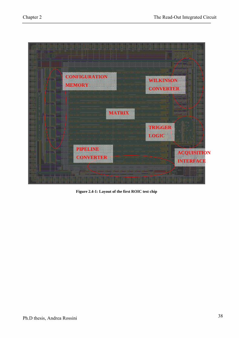
2.4 Layout of the test chip
The layout of the first test chip is depicted in Figure 2.4-1 in which the main blocks of the
system are highlighted. In particular, it is possible to note in the middle the huge matrix of
acquisition channels. The Wilkinson and the pipeline converters are located on the right and on
the bottom sides of the matrix respectively. The LTL, the GTL and the Acquisition Interface are
under the Wilkinson converter, while the memory for storing the configuration of the analog
acquisition channels (Configuration Memory) is on the left side of the matrix.
Due to the large number of connections with the back-end of the ASIC, only the first two metal
levels have been used inside each single pixel read-out cell, while the other metal levels have
been employed to ensure connections on the top level.
The clocked circuits have been arranged on the top-right corner of the ASIC and shielded with
many guard-rings. Furthermore, the routing has been kept wider than the minimum allowed from
the technology rules in order to reduce resistive paths.
The empty areas have been filled with filtering capacitors, placed between the power supply and
the ground lines. Different power pins have been placed for each block of the chip in order to
avoid any spike from the digital part to the analog one. This solution allows also monitoring the
power consumption of each block.
The microphotograph of the ROIC ASIC is shown in Figure 2.4-2. The resulting chip area is
equal to 8.6 x 7.2 mm2.
Chapter 2 The Read-Out Integrated Circuit
Ph.D thesis, Andrea Rossini 38
Figure 2.4-1: Layout of the first ROIC test chip
MATRIX
PIPELINE
CONVERTER
TRIGGER
LOGIC
WILKINSON
CONVERTER
CONFIGURATION
MEMORY
ACQUISITION
INTERFACE

Chapter 2 The Read-Out Integrated Circuit
Ph.D thesis, Andrea Rossini 39
Figure 2.4-2: Microphotograph of the ASIC ROIC

Chapter 2 The Read-Out Integrated Circuit
Ph.D thesis, Andrea Rossini 40

Chapter 3 The Wilkinson A/D Converter
Ph.D thesis, Andrea Rossini 41
Chapter 3
The Wilkinson A/D Converter
In this chapter we describe the Wilkinson A/D converter, and the solutions adopted to obtain the
desired specifications.
3.1 Introduction
The Wilkinson converter is a slow A/D converter able to handle a large number of acquisition
channels at the same time, thus allowing to support a large event rate in a sensor array in spite of the
long conversion time.
In ROIC test chip, described in Chapter 2, we have placed 16 Wilkinson converters, one for each
row of the 16x16 array of detectors. Each converter handles the output of the 16 pixels of the row.
In case of multiple events on the same row, the Trigger Logic implemented on the chip is able to
handle the priority of the events, [13], [39].
The main characteristics of the Wilkinson converter are:
• INL lower than ±0.5LSB;
• DNL lower than ±0.25LSB;
• Clock frequency equal to 50 MHz;
• Input range equal to 1.2 V;
• Resolution larger than 9 bit.
The block diagram of the Wilkinson A/D converter (ADC) are shown in Figure 3.1-1. The converter
consists of an input buffer, a voltage comparator, an output register, a ramp generator, a counter and
a clock generator. The ADC performs a voltage-to-time conversion of the input signal by using the
voltage ramp as reference to be compared with the output of the Peak and Hold circuit present in the
acquisition chain associated with each pixel of the matrix

Chapter 3 The Wilkinson A/D Converter
Ph.D thesis, Andrea Rossini 42
Figure 3.1-1: Wilkinson A/D converter block diagram
During the conversion process, the voltage comparator compares the output of the ramp generator
with the input signal, which is a constant voltage proportional to the incident photon energy. If the
Start Of Conversion (SOC) is at the high logic level, the value of the output register is stored when
the ramp becomes higher than the input signal. The value of the register represents the digital
conversion of the signal itself. When the counter reaches the last value, it is reset to the initial value.
The clock is provided as a differential sinusoidal waveform whose amplitude is 300 mV, centred
around 1.5 V with a frequency equal to 50 MHz. This solution has been adopted in order to avoid
any noise problems due to undesired glitches related to the rising edge of the clock signal.
Moreover, there is the possibility to program the slope of the ramp signal with a resolution of 7 bit
by means of the configuration memory.
The A/D converter achieves a complete conversion in a time ranging from 20 µs to 40 µs depending
if the conversion starts at the beginning of the ramp period or at the end. Indeed, two ramp periods
are actually used for the conversion in order to avoid spurious zero-crossings of the comparator due
to the settling of the input signal (i.e. the zero-crossing with the second ramp period after SOC is
used for the actual conversion), [14], [15].
An example of the conversion cycle is shown in Figure 3.1-2.
Chapter 3 The Wilkinson A/D Converter
Ph.D thesis, Andrea Rossini 43
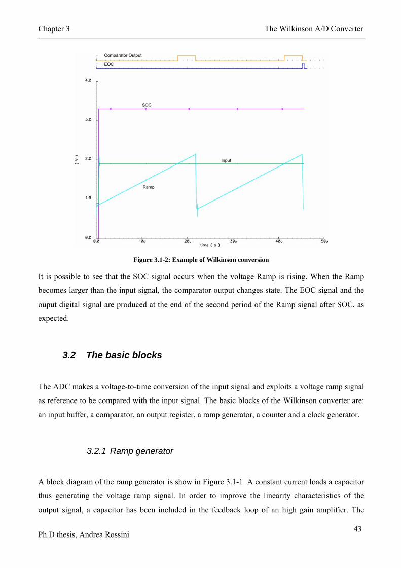
Figure 3.1-2: Example of Wilkinson conversion
It is possible to see that the SOC signal occurs when the voltage Ramp is rising. When the Ramp
becomes larger than the input signal, the comparator output changes state. The EOC signal and the
ouput digital signal are produced at the end of the second period of the Ramp signal after SOC, as
expected.
3.2 The basic blocks
The ADC makes a voltage-to-time conversion of the input signal and exploits a voltage ramp signal
as reference to be compared with the input signal. The basic blocks of the Wilkinson converter are:
an input buffer, a comparator, an output register, a ramp generator, a counter and a clock generator.
3.2.1 Ramp generator
A block diagram of the ramp generator is show in Figure 3.1-1. A constant current loads a capacitor
thus generating the voltage ramp signal. In order to improve the linearity characteristics of the
output signal, a capacitor has been included in the feedback loop of an high gain amplifier. The

Chapter 3 The Wilkinson A/D Converter
Ph.D thesis, Andrea Rossini 44
latter supplies all the current required by the following stage. In order to ensure a constant slope of
the ramp in the useful input range of the converter, the swing of the ramp signal has been extended
from 800 mV to 2.15 V, but only the central part of this range is actually used. In this way, it is
possible to neglect the second order effects and the glitches during the reset phase of the capacitor.
The value of the input current is programmed by a 7-bit DAC, controlled from the configuration
memory of the chip. The DAC has been implemented with cascode current mirrors in order to
guarantee the maximum output resistance and linearity. In order to obtain a slope of 60 V/μs, i.e.
required value to ensure the proper operation of the converter, the output current of the DAC has to
be equal to 1 μA, considering a capacitor of 18 pF.
Slope
Ib
C
-
+
Vout
CurrentDAC
Figure 3.2-1: Block diagram of the ramp generator
The overall useful output swing is 1.2 V (from 0.9 V to 2.1 V). The operational amplifier used is
based on a folded cascode architecture, as in the pipeline converter described in Chapter 4. The gain
of the amplifier is 83 dB with a GBW equal to 100 MHz.
3.2.2 Voltage Comparator
The schematic diagram of the voltage comparator used in the Wilkinson A/D converter is shown in
Figure 3.2-2. It is similar to a mirrored operational amplifier, but we added transistors M10 and M11
to obtain a positive feedback loop, which boosts the response time. These two transistors are also
used to introduce a slight hysteresis.

Chapter 3 The Wilkinson A/D Converter
Ph.D thesis, Andrea Rossini 45
M1 M2
M3 M4
M5
M6
M7
M8
M9
M11M10
MB
IBIAS
IN - IN + Vout
VDD
GND
Figure 3.2-2: Comparator schematic diagram
The output current of the comparator is given by
6
62
4
4
out mM in
WlI g V
Wl
⎛ ⎞⎜ ⎟⎝ ⎠= • •
⎛ ⎞⎜ ⎟⎝ ⎠
(3.1)
where W, l, gm are the width, the length and the tranconductance of the transistors, respectively. The
voltage gain turns out to be
( )6
62 7 6
4
4
//outout out mM ds ds
in
WlV R I g r rV W
l
⎛ ⎞⎜ ⎟⎝ ⎠= • = • •
⎛ ⎞⎜ ⎟⎝ ⎠ (3.2)
where r is is the drain to source resistance.
When applying the threshold voltage VG1 at the gate terminal of M1, and Vin at the gate of M2, with
Vin < VG1, M1 is on while M2 is off. In these conditions, M3 and M10 are turned on, while M4 and
M11 are off.

Chapter 3 The Wilkinson A/D Converter
Ph.D thesis, Andrea Rossini 46
All the current i5 flows through M1 and M3, and the drain voltage of M4 is close to Vdd, thus forcing
Vout to be close to ground. When Vin overcomes the threshold voltage, i5 begins to flow through M2
until it becomes equal to the current flowing into M10. At this point, the comparator output changes.
Most of the current flows into M2 and M4, thus causing M11 to be turned on and M3 and M10 off.
When Vin decreases and becomes lower than the threshold voltage, i5 begins to flow through M1.
The comparator output changes when i1 equals i11 (the current flowing through M11).
It is worth to point out that the hysteresis is controlled by ratios β10/β3 and β11/β4, related to
transistors M10-M3 and M11-M4 respectively. These ratios have to be larger than 1.
If VREF is applied at the gate terminal of M1 and the ratios β10/β3 and β11/β4 have the same value,
hysteresis turns out to be centred at VREF as shown in Figure 3.2-3.
To enhance the circuit performances, an output stage (i.e., transistors M6 and M7) and two inverters
have been added, thus obtaining sharp output transitions.
The transistors sizes are summarized in Table 3.2-1:
VREF V+V-
Vout
Vin
Figure 3.2-3: Comparator transfer function with hysteresis
Transistor W/L (μm/μm)
M1, M2, M3, M4 35/0.35
MB, M6, M7, M8, M9 40/0.35
M5 50/0.35
M10, M11 100/0.35
Table 3.2-1: MOS transistors sizes in the comparator

Chapter 3 The Wilkinson A/D Converter
Ph.D thesis, Andrea Rossini 47
3.2.3 The clock generator
The comparator structure discussed in the previous section has been used also in the clock
generator, by using as input signal a 300-mV sinusoidal differential waveform. The comparator
transforms this sinusoidal differential clock into a single-ended square wave, which is then used
throughout the chip.
To increase the speed of the comparator, the bias current has been slightly increased. This is not a
critical issue in the overall power budget, because the clock is common for all channels. Its power
consumption must be, hence, divided among all the used cells.
3.2.4 The counter and the output register
The counter has been designed to obtain a Gray code at the output. In this way, considering that the
comparator can change its state at any time independently of the clock signal, if we take the output
of the register before the settling transient after the clock rising edge is finished, we have an error
that is lower then 1LSB. The counter has been designed by using an automatic tool and then, with a
place and route program, inserted in the layout.
To implement the output register, ten flip-flops controlled with the comparator output as clock
signal have been adopted. At the rising edge of the comparator output, the register copies the output
of the counter. The Gray-to-binary conversion is performed at the output of the counter.
3.3 Measurement Setup
The measurements on the prototype chip have been carried out at the Alcatel Alenia Space LABEN
laboratories where a complete customized setup has been built.
The setup, shown in Figure 3.3-1, consists of standard instruments, like power supply, voltage
generators, voltmeters and oscilloscope. The ROIC ASIC, which includes the Wilkinson ADC, has
been hosted in a ad-hoc board with flash based FPGA for the readout procedure. To obtain the
digital acquisition we used a PC which implements some automatic procedures. Moreover, we have
used a National Instruments Acquisition Board and a MIO PCI Configuration Board.

Chapter 3 The Wilkinson A/D Converter
Ph.D thesis, Andrea Rossini 48
Figure 3.3-1: The measurements setup
A screen-shot of the acquisition tool is shown in Figure 3.3-2.

Chapter 3 The Wilkinson A/D Converter
Ph.D thesis, Andrea Rossini 49
Figure 3.3-2: Automatic acquisition tool developed at Alcatel Alenia Space LABEN laboratories
3.4 Experimental results
The chip has been measured to verify its correct operation. First of all, we verified the functionality
of the system with a single input signal. Figure 3.4-1 shows the measured waveforms obtained
during the Wilkinson ADC conversion cycle. It is possible to note the Start of Conversion signal
(SOC, channel 4) in the middle of the voltage ramp period, the ramp signal itself (channel 1) and the
End of Conversion (EOC, channel 3).

Chapter 3 The Wilkinson A/D Converter
Ph.D thesis, Andrea Rossini 50
Figure 3.4-1: Waveforms of the Wilkinson ADC conversion cycle
To verify the linearity of the ADC in the acquisition chain, we applied an input signal directly to the
converter through a dedicated multiplexer implemented on-chip.

Chapter 3 The Wilkinson A/D Converter
Ph.D thesis, Andrea Rossini 51
Figure 3.4-2: DNL (a) and INL (b) of the Wilkinson A/D converter
The DNL and INL of the A/D converter, depicted in Figure 3.4-2, are of the order of ±0.5LSB and
±0.6LSB respectively with a resolution of 10 bit.
Figure 3.4-3:DNL (a) and INL (b) of the complete acquisition chain
b)a)
a)
b)

Chapter 3 The Wilkinson A/D Converter
Ph.D thesis, Andrea Rossini 52
To verify the DNL and the INL of the entire acquisition chain, a pulse generator was used to
simulate the signal from the detector, with a rise time of 100 ns, duration 50 µs, fall time of 200 µs,
a pulse rate of 500 Hz and with amplitude varying continuously (ramp mode) between 50 mV and
1795 mV and a duration set to 900 s. The equivalent charge range is deemed about 300 to 11200
electrons.
From this measurement the DNL of the end-to-end chain is in the order of ±0.2LSB, and the INL in
the order of ±3.3LSB, as shown in Fig. 3.4-3.
Figure 3.4-4: Spectrum of the Wilkinson chain
Figure 3.4-4 shows an energy spectrum obtained by applying different input signals to the whole
chain. We considered 10 peaks with amplitudes ranging from the minimum detectable signal to near
the maximum ADC code, which correspond to a charge signal varying from 144 e- to 10300 e-. The
width of the peaks leads to an input referred noise as low as 34 e-.
The offset and the gain of the chains have been also measured. The output of the peak and hold has
been evaluated both with the internal ADC and with an external multichannel analyzer (MCA), as
shown in Figure 3.4-5 and Figure 3.4-6.

Chapter 3 The Wilkinson A/D Converter
Ph.D thesis, Andrea Rossini 53
Figure 3.4-5: Offset of the Wilkinson converters.
It is possible to notice the correlation between the two data set: the variation in the offset levels at
the output of the peak and hold is directly reflected into the ADC output code.
Also the gain of the various channels with the ADC has been evaluated to understand if there was
any spread due to the process or not. The correlation suggests that the ADC gain variation between
channels has a negligible effect with request to the gain variation within the front-end electronics.
Figure 3.4-6: Gain of the Wilkinson converter

Chapter 3 The Wilkinson A/D Converter
Ph.D thesis, Andrea Rossini 54
The power consumption of the whole chain is 0.9 mW while the power consumption of one A/D
converter stand alone is about 0.4 mW.
3.5 Conclusions
In this chapter we have presented a Wilkinson A/D converter able to resolve 10 bit. The main
characteristic of the converter are:
• INL lower than ±0.5 LSB;
• DNL lower than ±0.6 LSB;
• Clock frequency 50 MHz;
• Input range 1.2 V.
The basic blocks of the Wilkinson converter are: an input buffer, a comparator, an output register, a
ramp generator, a counter and a clock generator.
For every row of channels of the pixel matrix there is one Wilkinson A/D converter. Therefore, each
Wilkinson converter serves sixteen pixels and its power consumption is averaged, thus allowing to
maintain the overall power consumption lower than 1 mW per channel.
The A/D converter has been measured to evaluate its performance both as stand-alone cell and
inside the acquisition chain. The DNL and INL obtained considering the whole acquisition chain are
lower than ±0.2LSB and ±3.3LSB, respectively with a resolution equal to 10 bits.
The offset and gain spread between the different channels is not substantial. The input referred
noise achieved in the whole chain is as low as 34 e-.

Chapter 3 The Wilkinson A/D Converter
Ph.D thesis, Andrea Rossini 55

Chapter 4 Clock-less Pipeline-Like A/D Converter
Ph.D thesis, Andrea Rossini 56
Chapter 4
Clock-less Pipeline-Like A/D Converter
In this chapter the pipeline-like A/D converter structure is presented and discussed. The peculiarity
of this converter is the absence of the clock signal. Indeed, it acts as a combinatory logic, thus
avoiding the presence of a synchronization signal for all stages.
4.1 Introduction
The pipeline-like A/D converter realized is a fast A/D converter without clock, able to convert all
the data arriving from the pixel matrix with a latency time lower than 1 μs. Peculiarity of this
converter is the absence of a clock signal, that leads a significant reduction of the noise introduced
by the synchronization signal (clock) typical in the traditional high-speed A/D converter
implementations. The absence of the clock introduces the disadvantage of the lack of a signal that
indicates the end of the conversion. To be able to synchronize the output data, therefore we realized
an analog delay cell that emulates the latency of the converter, [16].
This cell is excited by the Start of Conversion (SOC) signal and generates an End of Conversion
(EOC). The delay introduced has to ensure the complete conversion of the input data also in the
worst process corners. The idea to realize a converter without clock arises from the ascertainment
that a traditional pipeline A/D converter for static signals acts as a sequential machine. The
innovative idea is in changing the approach to the conversion systems, passing from a sequential
operation of several cells to a combinatorial operation of the circuit. Actually, the data at the input
enters into the chain which evolves until it reaches a steady state, provided that the input signal
remains constant (this is the case in the ROIC chip since the input signal to the A/D converter is
provided by a peak and hold circuit). The block diagram of the ADC is shown in Figure 4.1-1. The
output of the first stage evolves with the time dictated mainly from the residue amplifier. The
second stage begins to work on the output of the first stage when it is not yet stable and, therefore,
the time required to reach the steady state turns out to be smaller than in a traditional
implementation with clock. Moreover the successive stages do not have to wait for the end of the
operation of the previous stages and can begin their conversion, limiting the dead-times required in

Chapter 4 Clock-less Pipeline-Like A/D Converter
Ph.D thesis, Andrea Rossini 57
a traditional architecture to accommodate the worst cases. When the steady state is reached, the
digital output is the exact conversion of the input data, [17], [18].
For this A/D converter we have used 9 stages which resolve 1.5 bit for stage, with a final 2 bit flash
stage. The error correction logic is needed for the recombination of the bits, as is possible to see in
Figure 4.1-1.
The GlobTrigD signal is needed to synchronize the data with the Trigger Logic.
Figure 4.1-1: Block diagram of the pipeline converter
The choice to use 1.5 bit per stage with digital correction logic allows us to tolerate a larger offset
in the comparators used in each stage, [19].
4.1.1 Error on the gain of the amplifier
Let us consider the case of a non ideal 1.5 bit cell, with an error in the amplifier gain, [20]. We
have:
( )2 1 AA E= −i (4.1)
where EA is the gain error . The cell transfer characteristic is shown in Figure 4.1-2

Chapter 4 Clock-less Pipeline-Like A/D Converter
Ph.D thesis, Andrea Rossini 58
Figure 4.1-2: 1.5 bit cell transfer characteristic
Considering a signal applied at the input of the stage equal to
4ref
inVV V= − Δ (4.2)
where ΔV is small compared to Vref/4, the digital output is D = 01 and the DAC output is VDAC = 0.
At the output of the amplifier holds:
( ) ( )2 14 4ref ref
out in DAC AV VV A V V A V A E⎛ ⎞= − = − Δ = −⎜ ⎟
⎝ ⎠i i i i (4.3)
where ΔV has been neglected.
The amplitude error is EAVref/2. In the worst case, if the ADC threshold has an error equal to -Vref/4,
the error turns out to be EAVref.
If n’ is the resolution left after the cell, to obtain an error lower than x LSB the following has to be
satisfied
'2 2nA ref refE V x V−<i i i (4.4)
The gain error leads to a shift in the level and then a loss in the output code. To obtain an INL
between ±½LSB, it is necessary to have x= ½ , thus obtaining:
'2 nAE −< (4.5)
If we have 10 bit of resolution, for the first cell we have n’=9. Than the maximum error is:
9 32 2 10AE −< − • (4.6)

Chapter 4 Clock-less Pipeline-Like A/D Converter
Ph.D thesis, Andrea Rossini 59
4.1.2 Error on the DAC level
If we consider an offset ΔVDAC on the ideal VDAC, the error at the output of the amplifier turns out to
be equal to 2ΔVDAC. By following a mathematical approach as the one discussed in the previous
section, we obtain
'2n
DAC refV x VΔ < i i (4.7)
With A = 2 (we have supposed no error in the amplifier gain) and x = ½, we have
9 22 2 2
refDAC
V LSBV +Δ < =i (4.8)
Since the difference between VDAC and Vin, directly affects the input of the cell, each error on the
DAC level in the first stage will affect the output of the second. Since for every stage the error is
amplified by a factor of two, it is mandatory that the error on the first cell is compatible with the
resolution of the complete converter. This means also that for each stage following the first one the
requirements about the maximum error tolerated double respect with the previous stage.
4.1.3 Error in the comparator threshold
In order to understand the effect of an error on the comparator threshold, we can look at the ideal 1
bit per stage cell and consider an input swing equal to 1 V, obtaining the situation in Figure 4.1-3,
[21].
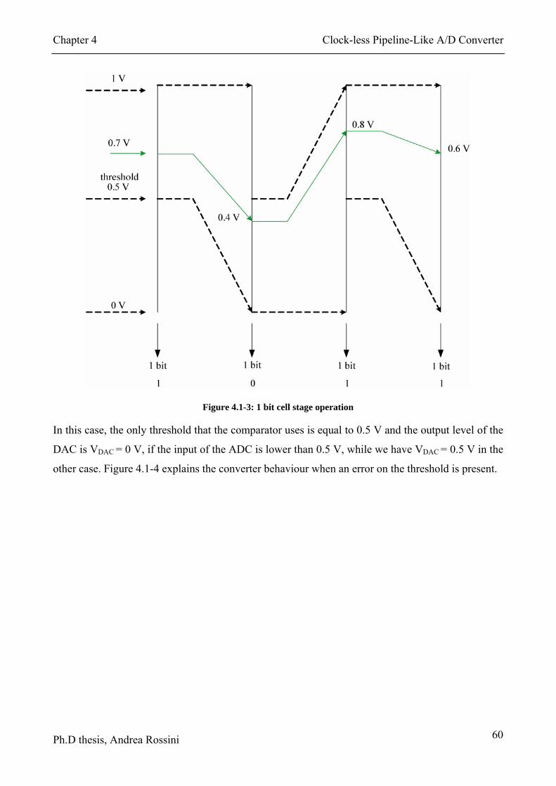
Chapter 4 Clock-less Pipeline-Like A/D Converter
Ph.D thesis, Andrea Rossini 60
Figure 4.1-3: 1 bit cell stage operation
In this case, the only threshold that the comparator uses is equal to 0.5 V and the output level of the
DAC is VDAC = 0 V, if the input of the ADC is lower than 0.5 V, while we have VDAC = 0.5 V in the
other case. Figure 4.1-4 explains the converter behaviour when an error on the threshold is present.

Chapter 4 Clock-less Pipeline-Like A/D Converter
Ph.D thesis, Andrea Rossini 61
Figure 4.1-4: 1 bit cell operation with error on the threshold
Due to the error on the threshold we have a wrong conversion of the input data and a negative
residue Vres, equal to:
( )2 0.4 0.5 0.2ResV = − = −i ( 4.9)
The resulting residue is out of the input swing for the next stage. The next stage will give a negative
output again, since there is no possibility to recover from this error (Vres2=2(-0.2-0.5)=-1,4 V).
Instead, if we use a 1.5 bit per stage architecture, we have three decision zone, thanks to the two
comparators and we are able to recover from this problem using a suitable logic to recombine the
bits produced by the different stages. Basically, we are adding redundancy, which is useful to
recover from the error. The output of the residue amplifier that has an maximum amplitude lower
than in the 1 bit case and, therefore, the amplifier avoids saturation even with an error in the
threshold level. Figure 4.1-5 shows the ideal operation of a 6 bit A/D converter with 1.5 bits per
stage, while Figure 4.1-6 illustrates the case in which a threshold error is present.

Chapter 4 Clock-less Pipeline-Like A/D Converter
Ph.D thesis, Andrea Rossini 62
Figure 4.1-5 : Ideal 6 bit A/D converter output with 1.5 bits per stage
0010 00 01 00 01
00 0 0 11
0.5V
-0.125V
0V
-0.5V
-0.125V
-0.4V
-0.3V
-0.1V
-0.2V
-0.1V
Figure 4.1-6: 6 bit A/D converter output with 1.5 bits per stage and offset on a threshold
From Figure 4.1-6 we can notice that the converter can recover at the fourth stage from the initial
error.
In order to obtain the proper digital code at the output from the bits produced by the different
stages, we need an error correction logic, which basically adds the different bits according to Table
4.1-1.

Chapter 4 Clock-less Pipeline-Like A/D Converter
Ph.D thesis, Andrea Rossini 63
b17 b16 +
b15 b14 +
b13 b12 +
b11 b10 +
b09 b08 +
b07 b06 +
b05 b04 +
b03 b02 +
b01 b00 =
O09 O08 O07 O06 O05 O04 O03 O02 O01 O00
Table 4.1-1: The error correction logic function characteristic
4.2 Basic blocks
The A/D converter consists of 9 1.5 bit stages and a final 2 bit flash stage, [22].
The 1.5 bit cells are composed by a flash ADC with 3 levels, a DAC and an amplifier. The analytic
expression of the amplifier output is
( )2out in DACV V V= −i (4.10)
which is graphically reported in Figure 4.2-1.

Chapter 4 Clock-less Pipeline-Like A/D Converter
Ph.D thesis, Andrea Rossini 64
Figure 4.2-1: Transfer characteristic 1.5 bit cell
To obtain a correct conversion, the first stage needs to have a residue with a precision higher than
the minimum signal detected by the converter. This is possible if the amplifier DC gain in the open
loop configuration is equal to 2KA = , where k is the resolution of the converter.
4.2.1 The ADC
Two types of ADC have been implemented in the pipeline converter, one used in the 1.5 bit cell and
one employed in the final flash stage. They are depicted in
-Vref 1.35 V
+Vref 1.65 V
Figure 4.2-2 and
-Vref 1.2 V
Vagnd 1.5 V
+Vref 1.8 V
Figure 4.2-3, respectively.

Chapter 4 Clock-less Pipeline-Like A/D Converter
Ph.D thesis, Andrea Rossini 65
-
+VLSB
Vin
-VRef
-
+VMSB+VRef
-Vref 1.35 V
+Vref 1.65 V
Figure 4.2-2: 1.5 bit ADC.
-
+
Vb2
Vin
-VRef
Vb1+Vagnd -
+
-
+
+VRef
-Vref 1.2 V
Vagnd 1.5 V
+Vref 1.8 V
Figure 4.2-3: 2 bits ADC
The comparator scheme is the same used in the Wilkinson A/D converter, which has been discussed
in Chapter 3. Also in this case an hysteresis has been introduced in the voltage comparator in order
to avoid oscillations due to noise when the input signal is close to the threshold. Even if this can be
considered as an offset added to the threshold, the error correction logic can compensate for the
introduced error.
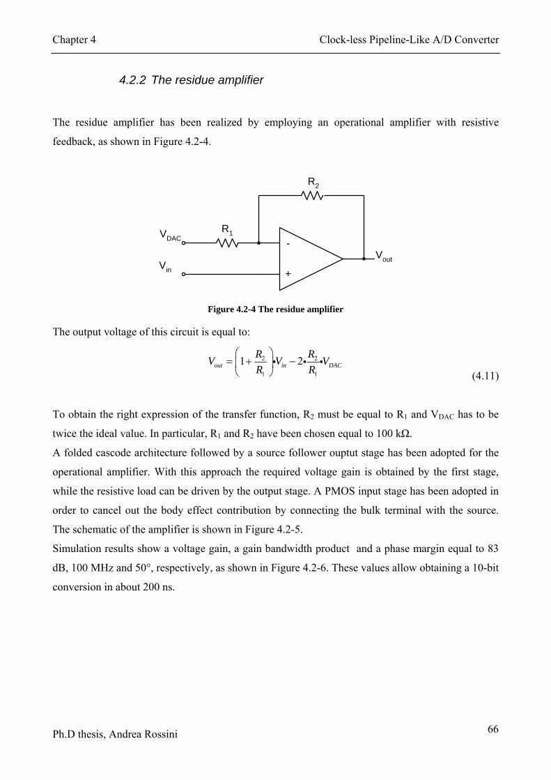
Chapter 4 Clock-less Pipeline-Like A/D Converter
Ph.D thesis, Andrea Rossini 66
4.2.2 The residue amplifier
The residue amplifier has been realized by employing an operational amplifier with resistive
feedback, as shown in Figure 4.2-4.
-
+
VoutVin
VDAC
R2
R1
Figure 4.2-4 The residue amplifier
The output voltage of this circuit is equal to:
2 2
1 1
1 2out in DACR RV V VR R
⎛ ⎞= + −⎜ ⎟
⎝ ⎠i i i
(4.11)
To obtain the right expression of the transfer function, R2 must be equal to R1 and VDAC has to be
twice the ideal value. In particular, R1 and R2 have been chosen equal to 100 kΩ.
A folded cascode architecture followed by a source follower ouptut stage has been adopted for the
operational amplifier. With this approach the required voltage gain is obtained by the first stage,
while the resistive load can be driven by the output stage. A PMOS input stage has been adopted in
order to cancel out the body effect contribution by connecting the bulk terminal with the source.
The schematic of the amplifier is shown in Figure 4.2-5.
Simulation results show a voltage gain, a gain bandwidth product and a phase margin equal to 83
dB, 100 MHz and 50°, respectively, as shown in Figure 4.2-6. These values allow obtaining a 10-bit
conversion in about 200 ns.

Chapter 4 Clock-less Pipeline-Like A/D Converter
Ph.D thesis, Andrea Rossini 67
Figure 4.2-5: Schematic of the operational amplifier used in the residue amplifier
The components sizes are summarized in Table 4.2-1.
Device Value
M1, M2 100/0.5 µm/µm
M3, M4 90/0.5 µm/µm
M5, M6 150/1 µm/µm
M7, M8 100/0.35 µm/µm
M9, M10 250/2 µm/µm
M11 300/0.35 µm/µm
M12 200/0.35 µm/µm
M13 260/0.35 µm/µm

Chapter 4 Clock-less Pipeline-Like A/D Converter
Ph.D thesis, Andrea Rossini 68
M14 90/0.35 µm/µm
M15 250/0.35 µm/µm
M16 2/0.35 µm/µm
Mb 450/0.35 µm/µm
R 3 kΩ
C 5 pF
Ibias 100 uA
Table 4.2-1: Design parameters of the operational amplifier used in the residue amplifier
Figure 4.2-6: DC gain and phase margin of the amplifier in open loop configuration
4.2.3 The DAC
The DAC has to produce the proper analog signal according to the bits bo and b1 provided by the
ADC. The precision required for the conversion from the digital to the analog domain influences
the value of the residue at the output of the cell. For the first stage, this precision must be higher
than VFS/2k, where k is the number of bits resolved by the stage, and VFS is the full scale voltage.
Figure 4.2-7 shows the circuit used for the DAC.

Chapter 4 Clock-less Pipeline-Like A/D Converter
Ph.D thesis, Andrea Rossini 69
Figure 4.2-7: Schematic of the DAC
The DAC output levels are:
V1 = 0.9 V
V2 = 2.1 V
Vagnd = 1.5 V
4.2.4 The EOC generator
The EOC generator, as mentioned above, has to delay the SOC signal. The generator consists of
two inverters, two comparator and an RC delay line, as shown in Figure 4.2-8.
Figure 4.2-8: EOC generator schematic diagram

Chapter 4 Clock-less Pipeline-Like A/D Converter
Ph.D thesis, Andrea Rossini 70
When a positive pulse occurs at the input node s_c, at the output of the first inverter holds
-1V
t
DDV e τ−= i (4.12)
where 1 3onMC Rτ = ⋅ (RonM3 is the on resistance of the NMOS M3 transistor) so that the voltage at
this node can rapidly decrease. At the output of the second inverter holds
( )- '
2V 1t
DDV e τ−= ⋅ − (4.13)
where τ’ =C2 * R2.
When V-1 reaches 1.5 V, the input of the second comparator switches to the high logic level. When
the SOC goes down, C1 starts to charge following this equation
( )- ''
1V 1t
DDV e τ−= ⋅ − (4.14)
where τ’’=R1C1
The output of the first inverter switches to the low logic level with a delay proportional to τ’’,
causing a fast discharge of C2 through the on resistance of the NMOS transistor. The circuit is able
to delay the rising edge and the falling edge with different delay values. In particular τ’ controls the
delay of the rising edge, while τ’’ the delay of the falling edge. For a correct timing, the edges have
to occur only when the output data is ready. To ensure the correct conversion in all process corners
in which the converter has been simulated, the EOC occurs after 700 ns.
4.3 Simulation Results
Let us assume that the input signal of the i-th stage is equal to the threshold voltage of one of the
two comparators of the ADC. As in any electronic circuit some noise is superimposed to the signal.
Every time the input signal, because of the noise, crosses the threshold voltage, the comparator
output changes state, thus producing a change in the output bits of the converter stage. These bits, in
turn, produce a change in the output voltage of the DAC, thus inducing a variation of the residue.
Therefore, a noise on the input signal when it is close to the threshold voltage of the ADC induces a
variation of the residue. This residue is the input of the next stage and therefore the noise is
propagated in all the stages of the converter. Moreover, if the output bits are stored after the adder,
additional noise is produced. In fact, if the adder never has stable inputs, it produces an output (the
digital conversion of the input value) that is continuously changing. The can produce an equivalent

Chapter 4 Clock-less Pipeline-Like A/D Converter
Ph.D thesis, Andrea Rossini 71
noise as large as the most significant bit (MSB). Simulating the A/D converter in Simulink with a
constant input equal to the high threshold of the ADC and with 1 LSB of superimposed noise, we
obtained the result shown in Figure 4.3-1, that illustrates the not corrected operation of the
structure.
Figure 4.3-1: Output of the converter with 1LSB noise on the input signal
The above drawbacks can be overcome by adopting the following solutions: introduce hysteresis in
the comparators of the ADC and store the converted bits before sending them to the adder. Different
kind of hysteresis have been simulated, either centered around the comparator threshold or shifted
towards the top or the bottom The converter has been simulated to estimate the DNL (Differential
Not Linearity) and the INL (Integral Not Linearity). In particular the DNL does not have to exceed
the value of 0.5 LSB (least significant bits).
The main simulation results are here summarized
• Hysteresis aligned at the bottom on both comparators
Passing from 200 mV to 210 mV of hysteresis the DNL becomes higher than 0.5 LSB.
• Hysteresis aligned at the top on both comparators
Passing from 140 mV to 150 mV of hysteresis the DNL becomes higher than 0.5 LSB.

Chapter 4 Clock-less Pipeline-Like A/D Converter
Ph.D thesis, Andrea Rossini 72
• Hysteresis aligned at the bottom on the high threshold comparator and hysteresis aligned at
the top on the low threshold comparator
Passing from 140 mV to 150 mV of hysteresis the DNL becomes higher than 0.5 LSB.
• Hysteresis centered on both comparators
Passing from 150 mV to 160 mV of hysteresis the DNL becomes higher than 0.5 LSB.
As it can be noticed, all the cases respect the 1.5-bit per stage theory of a A/D pipeline converter:
the digital correction technique corrects threshold errors up to VREF/4 (VREF = 0.6 V). The final
choice was to use a centered hysteresis around the threshold voltage level, because of its layout
symmetry. The amplitude of the hysteresis is set to 100 mV because it ensures a good robustness to
noise and at the same time it is lower than VREF/4 and hence it does not affect the linearity of the
conversion, obtaining in the same condition of 1 LSB noise over an input signal near the high
threshold of the DAC, the results shown in Figure 4.3-2.
Figure 4.3-2 : Output code of the 1LSB input noise at the converter with the hysteresis solution
The maximum error that we can have is one LSB on the final value, as expected with 1 LSB noise.

Chapter 4 Clock-less Pipeline-Like A/D Converter
Ph.D thesis, Andrea Rossini 73
Figure 4.3-3 : Converter structure with the Flip Flop Array
Figure 4.3-3 shows the modified structure of the converter. It is possible to see that the conversion
bits are sampled from the array of flip-flops controlled by the EOC signal before the error
correction logic. Subsequently the data are sent to the Ripple Carry Adder that carries out the sum
producing the 10 bits of conversion. The time required for the addition is equal to 9 tcarry where tcarry
is required for a full adder to produce the carry output. Therefore after approximately 9 tcarry from
the rising edge of the EOC signal we have the 10 bit word that constitutes the conversion of the
analog value at the input.
The maximum error that we obtain also in this case with 1 LSB noise superimposed to the signal is
one LSB, as shown in Figure 4.3-4.

Chapter 4 Clock-less Pipeline-Like A/D Converter
Ph.D thesis, Andrea Rossini 74
Figure 4.3-4: Output code of the converter with 1 LSB noise superimposed to the input signal with the flip-flop
array
The simulated DNL and INL of the converter are shown in Figure 4.3-5 and Figure 4.3-6.

Chapter 4 Clock-less Pipeline-Like A/D Converter
Ph.D thesis, Andrea Rossini 75
Figure 4.3-5: DNL of the converter
Figure 4.3-6: INL of the converter

Chapter 4 Clock-less Pipeline-Like A/D Converter
Ph.D thesis, Andrea Rossini 76
The converter has been simulated also in the process corners, as shown in Table 4.3-1, where tm=
typical case, ws=worst speed, wz=worst zero, wo=worst one, wp=worst power, achiving results
within specifications.
Corner Model transistor CMOS
Model resistance
Model capacitor Temperature
Corner 1 tm tm tm 27° C
Corner 2 tm tm tm 80° C
Corner 3 tm tm tm -20° C
Corner 4 wp wp wp 27° C
Corner 5 wp wp wp -20° C
Corner 6 ws ws ws 27° C
Corner 7 wo wp wp 27° C
Corner 8 wz wp wp 27° C
Corner 9 wo ws ws 27° C
Corner 10 wz ws ws 27° C
Corner 11 ws ws ws 80° C
Table 4.3-1: Process Corners
4.4 Experimental results
A test chip of the pipeline-like A/D converter has been fabricated in a 0.35 µm CMOS and has been
measured to evaluate either static (INL & DNL) and dynamic (SNR & ENOB) performance
parameters. An external sample and hold was used to match the configuration of the final
spectrometry application.
Figure 4.4-1 and Figure 4.4-2 show the measured DNL (within ±1.2LSB) and INL (within ±2.5
LSB), respectively.

Chapter 4 Clock-less Pipeline-Like A/D Converter
Ph.D thesis, Andrea Rossini 77
Figure 4.4-1: DNL of the converter
Figure 4.4-2: INL of the converter

Chapter 4 Clock-less Pipeline-Like A/D Converter
Ph.D thesis, Andrea Rossini 78
Figure 4.4-3: Spectrum of the converter
A typical FFT spectrum measured with an 80 kHz input sine wave at 400kS/s is reported in Figure
4.4-3. Notice that operating with a ratio fin/Fs=1/5 corresponds to have large steps between
consecutive samples, and this could be critical for a clock-less ADC. In addition an external sample
and hold is not perfectly suitable for this timing-less converter. However, in this case a SNR=55.4
dB (i.e. an ENOB = 8.91b) is achieved.
Figure 4.4-4 shows the microphotograph of the test chip, whose size is 2.4 mm2.
Figure 4.4-4: Microphotograph of the pipeline-like A/D converter
The values obtained for the INL and DNL and the conversion time obtained make this converter not
completely suitable for the desired application. A possible solution is to increase the current in
order to fulfil the speed requirements, thus worsening the power consumption of the converter.

Chapter 4 Clock-less Pipeline-Like A/D Converter
Ph.D thesis, Andrea Rossini 79
Anyhow, for the implementation of the final ROIC chip, we decided to use the Wilkinson A/D
converter described in Chapter 3.
4.5 Conclusion
A 10 bit pipeline-like A/D converter without clock for X-ray spectrometry is presented. The
converter is able to convert an input signal in 2.5 μs and achieves almost 9 bits of effective
resolution. The structure consist of 9 1.5 bit stages and a final 2 bit flash stage. The structure acts
like a combinatory logic, propagating the residue asynchronously along the stages. An EOC
generator is needed to indicate when the conversion is finished.
The overall features of the converter are summarized in the following outline:
• Power consumption 95 mW (12 [email protected] )
• DNL ± 1.2 LSB
• INL ± 2.5 LSB
• SNR 55.4 dB
• Conversion time 2.50 μs

Chapter 4 Clock-less Pipeline-Like A/D Converter
Ph.D thesis, Andrea Rossini 80

Chapter 5 Magnetic Sensor Model
Ph.D thesis, Andrea Rossini 81
Chapter 5
Magnetic Sensor Models
In this chapter different kinds of magnetic sensors will be discussed together with the possibility to
create a model that can help the designer during the development of an integrated sensor system.
The attention will be focused on four types of magnetic sensors: hall devices, magneto-resistance,
flux-gate and magneto-inductance.
The models will be compared with a real sensor to validate the model itself.
5.1 Introduction
Magnetic sensors have been used since hundreds of years. At the beginnings they were available
only as mechanical devices for navigation and orientation in open spaces. Recently to detect a
magnetic field it is possible to use both mechanical and electronic sensors. The main advantage of
the electronic sensors, which have been recently developed, is that they can be integrated together
with electronic interface circuits in the data processing flow. There are several types of magnetic
sensors, but, basically, all of them, when detecting a magnetic field, show a small variation of a
physical property or parameter of the device. The entity of this variation, which is related to the
sensitivity of the sensor to the magnetic field applied, makes the sensor itself suitable for a specific
type of application. It is thus possible to classify the magnetic sensors by using their field sensing
range. As shown in Table 5.1, three categories can be identified: low field, medium field, and high
field sensors. Magnetic fields less than 1 μgauss (where 1 gauss = 100 μT) are very low and well
below the Earth magnetic field. Sensors with a range of 0.1 gauss to few gauss will be considered
Earth’s field sensors and sensors with sensitivity above 10 gauss can be considered bias magnet
field sensors. For measuring the Earth magnetic field with devices that are suitable for portable
applications, the magneto-resistance and magneto-inductance (to be used as discrete sensors) are
available as well as the Fluxgate magnetic sensors. Fluxgates and magneto-resistances require using
magnetic material. They, as well as magneto-transistor and Hall sensors, can be integrated by using
CMOS technologies. It has to be pointed out that the use of magnetic material as concentrator can
help in increasing their sensitivity. Fluxgate, Hall sensor with magnetic concentrator, magneto-

Chapter 5 Magnetic Sensor Model
Ph.D thesis, Andrea Rossini 82
transistors allow achieving 2D on chip,[23]. By contrast, conventional Hall devices are for 1D.
Each sensor has specific characteristics that make it suitable for a given range of applications. In
addition to the sensitivity, it is necessary to take into account the range of temperature, the sensor
volume, and its on-chip manufacturability.
Table 5.1: Classification of magnetic sensors
Nowadays there are several different applications where magnetic sensors can be used. Among
them electronic compasses, sensors for traffic control, magnet activated switches for cellular
phones, and notebooks or handheld devices can be mentioned. Other applications are in the
automotive field or home appliances: devices based on magnetic sensors are used, for example, to
control the car engine or apparatus used in domestic ambient.[24]
In order to be able to design circuits for a particular application, which requires also magnetic
sensors, it is thus important to have tools able to properly describe the behaviour of magnetic
sensors.
5.2 Types of magnetic sensors
As shown in Table 5.1, there are several magnetic sensors that use different technologies to detect
magnetic field. The principles of operation of the most used types of magnetic sensors are listed
below.

Chapter 5 Magnetic Sensor Model
Ph.D thesis, Andrea Rossini 83
5.2.1 Squid
The magnetic sensor with the highest sensitivity is the Superconducting Quantum Interface Device
(SQUID). Developed around 1962, it is able to detect magnetic fields from few fempto-Tesla to
tens of Tesla. It is used in medical applications since it can detect the human brain neuro-magnetic
field (about few femptoTesla). The main drawback of such a sensor is the low temperature of
operation (about 4 K) needed to cool down the junction required to measure the current induced by
the magnetic field.
5.2.2 Search-coil
Search coils are based on the induction Faraday law, that establishes that the induced voltage in a
coil is proportional to the variation of the magnetic field concatenated to the same coil. This voltage
creates a current that is proportional to the speed of the variation of the field itself. The sensitivity
of the search-coil depends on the properties of the magnetic material used, the area of the coils and
the number of coils used. The direct application of the Faraday law makes this sensor not suitable
for static or slow frequency fields.
5.2.3 Magneto-inductive sensor
The magneto-inductive sensor is a new type of magnetic sensor developed about fifteen years ago.
Nowadays it is one of the cheapest and most used sensor thanks to its reliability. For this reason, a
model of such a sensor has been developed and will be discussed in this chapter. The magneto-
inductive sensor is basically a solenoid with magnetic material inside. If a current flows inside the
solenoid, it generates a magnetic field and an induced voltage. By linking this voltage to the initial
current it is possible to obtain the value of the inductance of the sensor. An external magnetic field
Hext changes the value of the magneto-inductance, since it changes the value of the induced voltage
by the sensed magnetic field. By employing a circuit able to detect the value of the inductance, it is
possible to derive the value of an external magnetic field.

Chapter 5 Magnetic Sensor Model
Ph.D thesis, Andrea Rossini 84
5.2.4 Magneto-resistance
Magneto-resistive sensors are based on the anisotropic magneto-resistance effect (AMR) and have
been developed in the last 30 years, [25]. Magneto-resistive sensors exploit the fact that external
fields H influence the electrical resistance ρ of certain ferromagnetic alloys. This solid-state
magneto-resistive effect can be easily realized by using a thin film technology. The specific
resistance ρ of anisotropic ferromagnetic metals depends on the angle θ between the internal
magnetization M and the current I, according to
( ) ( ) ( )2|| cosp pρ θ ρ ρ ρ θ= + − (5.1)
where pρ and ||ρ are the resistivities perpendicular and parallel to M, [26]. The quotient
( )|| / /pρ ρ ρ ρ ρ− = Δ (5.2)
is called the magneto-resistive effect and may amount to several percent. Sensors are always made
of ferromagnetic thin films as this has two major advantages over bulk material: the resistance is
high and the anisotropy can be made uni-axial. The ferromagnetic layer behaves like a single
domain and has one distinguished direction of magnetization in its plane called the easy axis (e.a.),
which is the direction of magnetization without external field influence.
Figure 5.2-1: Geometry of a simple sensor
Figure 5.2-1 shows the geometry of a simple sensor where the thickness (t) is much smaller than the
width (W), which, in turn, is less than the length (L) (i.e. t « W ‹ L). With the current (I) flowing in

Chapter 5 Magnetic Sensor Model
Ph.D thesis, Andrea Rossini 85
the x-direction (i.e. θ = 0 or Θ = φ) the following equation can be obtained from (1)
( )20 cosR R R ϕ= + Δ (5.3)
and with a constant current I, the voltage drop in the x-direction Ux becomes
x pU Iρ= (5.4)
Besides this voltage, which is directly linked to the resistance variation, there is a voltage in the y-
direction, Uy, given by
y pU Iρ=
This is called the planar or pseudo Hall effect. It resembles the normal or transverse Hall effect but
has a physically different origin. The signal obtained from the sensor depends on the angle between
the magnetization M and the x-direction. If M changes due to external field H, this field determines
the sensor signal.
It is possible to show that
2
0
1 1 yx p
HLU IW t H
ρρρ
⎛ ⎞⎛ ⎞⎛ ⎞⎛ ⎞Δ⎛ ⎞ ⎜ ⎟⎜ ⎟= • • + • − ⎜ ⎟⎜ ⎟ ⎜ ⎟ ⎜ ⎟⎜ ⎟•⎝ ⎠ ⎝ ⎠ ⎝ ⎠⎝ ⎠⎝ ⎠ (5.5)
( )
1/ 22
0 0
/ 1y yy p
H HU I L t
H Hρρρ
⎛ ⎞⎛ ⎞Δ ⎜ ⎟= • • • • − ⎜ ⎟⎜ ⎟⎝ ⎠⎝ ⎠ (5.6)
In the case in which Hx ≠ 0, it is necessary to replace H0 with H0+ Hx/cos φ.
The main difference is that Ux depends on the square of Hy/H0 while the Hall voltage Uy is linear
for Hy<<H0, and the ratio of their maximum values is L/W, so that the Hall voltage is lower
(L>>w).
As shown in Eq. 5.5, the basic magneto-resistor has a square resistance-field (R-H) dependence, so
a simple magneto-resistive element cannot be used directly for linear field measurements. A
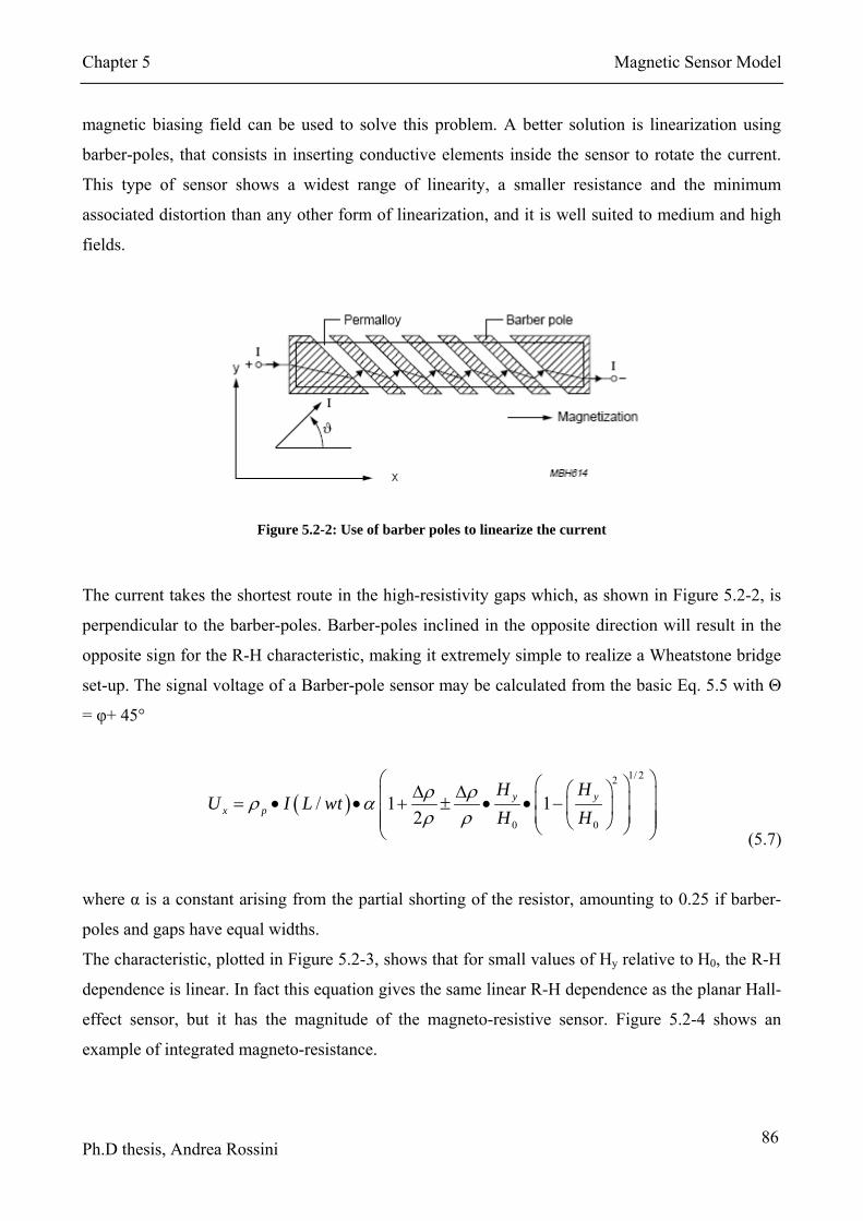
Chapter 5 Magnetic Sensor Model
Ph.D thesis, Andrea Rossini 86
magnetic biasing field can be used to solve this problem. A better solution is linearization using
barber-poles, that consists in inserting conductive elements inside the sensor to rotate the current.
This type of sensor shows a widest range of linearity, a smaller resistance and the minimum
associated distortion than any other form of linearization, and it is well suited to medium and high
fields.
Figure 5.2-2: Use of barber poles to linearize the current
The current takes the shortest route in the high-resistivity gaps which, as shown in Figure 5.2-2, is
perpendicular to the barber-poles. Barber-poles inclined in the opposite direction will result in the
opposite sign for the R-H characteristic, making it extremely simple to realize a Wheatstone bridge
set-up. The signal voltage of a Barber-pole sensor may be calculated from the basic Eq. 5.5 with Θ
= φ+ 45°
( )1/ 22
0 0
/ 1 12
y yx p
H HU I L wt
H Hρ ρρ αρ ρ
⎛ ⎞⎛ ⎞⎛ ⎞Δ Δ⎜ ⎟⎜ ⎟= • • + ± • • − ⎜ ⎟⎜ ⎟⎜ ⎟⎜ ⎟⎝ ⎠⎝ ⎠⎝ ⎠ (5.7)
where α is a constant arising from the partial shorting of the resistor, amounting to 0.25 if barber-
poles and gaps have equal widths.
The characteristic, plotted in Figure 5.2-3, shows that for small values of Hy relative to H0, the R-H
dependence is linear. In fact this equation gives the same linear R-H dependence as the planar Hall-
effect sensor, but it has the magnitude of the magneto-resistive sensor. Figure 5.2-4 shows an
example of integrated magneto-resistance.

Chapter 5 Magnetic Sensor Model
Ph.D thesis, Andrea Rossini 87
Figure 5.2-3: Effect of the barber poles (continuous line) and the normal sensor (dot line) versus magnetic field
Figure 5.2-4: An integrated magneto-resistance

Chapter 5 Magnetic Sensor Model
Ph.D thesis, Andrea Rossini 88
5.2.5 Hall sensor
The Hall effect was discovered by Dr. Edwin Hall in 1879. Dr. Hall found that when a magnet was
placed so that its field was perpendicular to one face of a thin rectangle of gold through which
current was flowing, a difference in potential appeared at the opposite edges. He found that this
voltage was proportional to the current flowing through the conductor, and the flux density or
magnetic induction perpendicular to the conductor. When a current-carrying conductor is placed
into a magnetic field, a voltage will be generated perpendicular to both the current and the field.
This principle is known as the Hall effect. Figure 5.2-5 illustrates the basic principle of the Hall
effect. It shows a thin sheet of semiconducting material (Hall element) through which a current
flows. The output connections are perpendicular to the direction of the current. When no magnetic
field is present, the current distribution is uniform and no potential difference is seen across the
output. When a perpendicular magnetic field is present a Lorentz force is exerted on the current.
This force disturbs the current distribution, resulting in a potential difference (voltage) across the
output. This voltage is the Hall voltage (VH).

Chapter 5 Magnetic Sensor Model
Ph.D thesis, Andrea Rossini 89
Figure 5.2-5: Effect of the magnetic field on the current
For the Lorentz’s law, a charged particle q moving inside the conductor in a magnetic field B with a
speed equal to vd, is subject to a force equal to:
dF q v B= ×i (5.8)
where × is the vectorial product operator between vd and B.
In stationary condition this force is balanced by the induced electrical field generated from a charge
redistribution, named Hall field HE. The integral of this field along the conductor gives the Hall
voltage VH. This voltage is equal to VH = EH W in the case that B is uniform along the conductor,
where W is the width. An electron placed inside the conductor is subject to a force equal to F =
qEH.
Using Eq.5.8, and using vd = -Jx/q, where Jxis the current density, it results
H dq E q v B=i i i (5.9)
that means
H H xE R J B= i i (5.10)

Chapter 5 Magnetic Sensor Model
Ph.D thesis, Andrea Rossini 90
where RH is defined as the Hall coefficient. By considering parameter r that takes into account
statistic variation of speed of the carrier (+ for electrons or – for holes)
H
rRq
= ± (5.11)
it is possible to express the Hall voltage as
810H H
I BV Vt
=ii
(5.12)
By using this equation it is possible to determine the type of carriers and the concentration. From
this values and knowing the current, it is then possible to obtain the conductivity and the Hall
mobility (μ = σ|RH|).
5.2.6 Fluxgate
Fluxgate sensors are among most used magnetometers thanks to their possibility to be integrated
together with microelectronic circuits. Fluxgate magnetometers were first introduced in the 1930’s.
Some development was for airborne magnetic surveys and for submarine detection, like Hall
devices. They were further developed for geomagnetic studies, for mineral prospecting and for
magnetic measurements in outer space. They have also been adapted and developed for various
detections and surveillance devices, both for civil and military use. Despite the advent of newer
technologies for magnetic field measurements, Fluxgate magnetometers continue to be used
successfully in all of these areas, thanks to their reliability, relative simplicity, and economy. In the
late 1950’s, the Fluxgate was adapted to space magnetometer applications. Even as early as 1948, a
three-axis Fluxgate was used in an Aerobee sounding rocket to a peak altitude of 112 km. The first
satellite to carry a magnetometer of any type was Sputnik 3 which was launched in 1958 and carried
a servo-oriented Fluxgate. Luniks 1 and 2 (Russian lunar probes), both launched in 1958, carried
triaxial Fluxgates. The USSR Venus probe launched in 1961 carried two single-axis Fluxgates. The
first American satellite to carry a Fluxgate was Earth orbiting Explorer 6 launched in 1959. Some
satellites or space probes carrying Fluxgate have included USSR Mars probe, Nasa Explorer 12, 14

Chapter 5 Magnetic Sensor Model
Ph.D thesis, Andrea Rossini 91
and 18, Mariner 2 (Venus) the USSR Earth-orbit Electron 2 and Apollo 12, 14, 15 and 16.
Nowadays, developments for this sensor are expected in the solution based on CMOS technology
for the coils and CMOS compatible post-process technology (i.e. sputtering) for the core deposition.
This way, it is possible to realize micro-Fluxgates featuring very low power consumption (in the
order of few mW) and minimum silicon area. They show some common point with magneto-
inductances due essentially to the common structure they have together. The basic structure of a
Fluxgate sensor, shown in Figure 5.2-6, consists of two coils: a primary (excitation) and a
secondary (sensing) coil, wrapped around a common high permeability ferromagnetic core.
Figure 5.2-6: Structure of a Fluxgate in a magnetic field
The excitation current Iexc flowing through the excitation coil produces a field that periodically
saturates the soft magnetic material core (in both directions). In saturation (Figure 5.2-6-b), the
permeability of the core drops and the DC flux associated with the DC magnetic field B0 to be
measured decreases. The name of the device derives from this “gating” of the flux that occurs when
the core is saturated. When the field to be measured is present, the 2nd harmonic, and also higher
order even harmonics, appears in the voltage Vind, induced in the sensing coil. This behaviour is
strictly related to the transfer function of the system that is the hysteresis loop of the magnetic field.
Without an external magnetic field, exciting the excitation coil with a current at frequency f, the
induced voltage will be due to the sum of different harmonics at frequency f, 3f, 5f, 7f, and so on,
according with the odd transfer function. When an external magnetic field is applied, the different
operating point degrades the symmetry in the transfer function and therefore, together with the odd

Chapter 5 Magnetic Sensor Model
Ph.D thesis, Andrea Rossini 92
harmonics, the even harmonics will appear. The amplitude of this even harmonics, that represent
the sensor output, will be proportional to the intensity of the external magnetic field. The amplitude
of the induced voltage is described by the Faraday’s law
( )0
sin 2 excexc
ind sens
f td N I
ldV N Sdt dt
πμ⎛ ⎞⎜ ⎟
Φ ⎝ ⎠= − = −
i ii i i
i i (5.13)
where Nsens and Nexc are respectively the number of turns of the sensing coil and of the excitation
coil, S is the cross section of the sensing coil, l is the length of the excitation coil, μ is the magnetic
permeability and I0·sin(2π·fexc·t) is the sinusoidal excitation current at frequency fexc. The sensor
sensitivity can be improved by maximizing the induced voltage, and this can be done using the
following solutions:
• by increasing the excitation frequency (fexc); however, an upper bound to fexc is given by the
cut-off frequency of the ferromagnetic material relative permeability;
• by increasing the number of turns of the sensing coil (Nsens);
• by increasing the cross section of the ferromagnetic material (S), considering that a larger
cross-section requires a larger current to saturate the ferromagnetic material and, hence, an
increased power consumption.
The main drawback of Fluxgate magnetic sensors realized with the coils wrapped around the core is
the complex construction of the core and of the coils when they have to be realized within planar
technologies. For this reason, new topologies of planar integrated micro-Fluxgate were recently
presented in the open literature. For instance, a structure for a differential single axis planar
Fluxgate magnetic sensor is shown in Figure 5.2-7. The ferromagnetic core is placed over the
diagonal of the excitation coil.

Chapter 5 Magnetic Sensor Model
Ph.D thesis, Andrea Rossini 93
Figure 5.2-7: Structure of a planar Fluxgate
Supplying the excitation coil with a suitable current, each half of the core periodically saturates in
opposite directions, as illustrated in Figure 5.2-8. When no external magnetic field is applied, the
two sensing coils, connected in antiseries, show an output voltage that ideally is zero. By contrast,
when an external magnetic field component is present and parallel to the core, the magnetization in
one half of the core is in the same direction as the external magnetic field, while the magnetization
of the other half of the core is in the opposite direction. Therefore, the voltage induced in the two
sensing coils is not the same and the differential output voltage increases its value, resulting in an
amplitude modulation. In Figure 5.2-8 three different cases are shown, when the external magnetic
field was not applied and applied with two different values.

Chapter 5 Magnetic Sensor Model
Ph.D thesis, Andrea Rossini 94
Figure 5.2-8: Effect of the magnetic field on the sensor output
5.3 The magnetic sensor model
In order to be able to simulate the electronic interface circuits together with the magnetic sensors, a
magnetic sensor model compatible with SPICE-like simulators has to be developed. The Analog
High-level Description Language (AHDL) code developed describes the behavioural model of four
different types of sensors: a magneto-resistance, a magneto-inductance, a hall device and a
Fluxgate.

Chapter 5 Magnetic Sensor Model
Ph.D thesis, Andrea Rossini 95
Struttura delcomponente e
comportamento(moduli)
Struttura del sistem a(netlist)Set di equazioni
Risposta del sistema
Figure 5.3-1:Structure used by simulator
In particular, the VERILOG-A language has been used
since it is suitable for the CADENCE simulation
environment, tool widely used for IC design. From a set of
equations it is possible to define the component behaviours.
This set of equation is taken by the simulator and inserted
into the netlist to obtain the behaviour of the complete
system and carry on the simulation. Of course, the more
accurate is the set of equation, the more accurate will be the
result of the simulation.
The symbol of the magnetic sensor is a 5-terminal
component. The meaning of some of the terminals can
change depending on the type of sensor. For all models two
main terminals have been introduced, one of which is the
reference, representing the electrical output of the sensor,
the other, the differential voltage across the main terminals
or the current through them is the effect of the magnetic
field. A voltage generator or a current source through a
third terminal represents the input of the device: the
external magnetic field, H. The remaining two terminals have been introduced for the pick-up coil
in Fluxgates or to monitor internal quantities for other sensors. A set of equations describes the
sensor operation. The model also includes non-idealities typical of real devices. Performance
depends on a number of parameters that are specified in the model card similarly to what is done for
Figure 5.3-2: Simulator model card

Chapter 5 Magnetic Sensor Model
Ph.D thesis, Andrea Rossini 96
active components. The global parameters for a given type of sensor are given in the sensor model
card.
5.3.1 Magneto-resistance
The magneto-resistance changes with external magnetic field, Hext. We assume that the output
variable is the voltage across the magneto-resistance, Vout. It is given by
( )0 1out extV R H Iα ρ= +i i i i (5.14)
where R0 is the resistance without external field, ρ is the resistance for unit of length and α is a
fitting parameter accounting for the different orientations between magnetization and current
flowing in the sensor.
The parameters that the designer can change are both geometrical, like the area and the length, but
also structural depending on the magnetic characteristics of the sensor, like the resistance R0 and the
internal magnetic field.
By using the circuit depicted in Figure 5.3-3 it is possible to evaluate the behaviour of the sensor.
Figure 5.3-3: Circuit for reading the output of the magneto-resistance

Chapter 5 Magnetic Sensor Model
Ph.D thesis, Andrea Rossini 97
This circuit consists of a Wheatstone bridge where the resistance R1A and R4A are equal and have
the barber-poles oriented in the opposite direction with respect to R2A and R3A. When the external
field changes, like in Figure 5.3-4 a), the magneto-resistance shows a variation with the magnetic
field, Figure 5.3-4 b). For small value of the external field, the difference output of the Wheatstone
bridge shows a linear variation in the transient response, Figure 5.3-4 c). The output of the sensor is
then amplified by the operational amplifier to make it usable for the following circuit, Figure 5.3-4
d).
Figure 5.3-4: Output of the simulated sensors: a) magnetic field applied, b) resistance of the sensor c) output of
the sensor d) output of the amplifier
5.3.2 Fluxgate
In the Fluxgate sensor a given current through a primary coil induces a voltage on the secondary
(pick-up) coils that depends on the external magnetic field Hext. The output variable is Vout, the
pick-up signal, [28]. The used equations are
1 extH n I Hα= +i i (5.15)
( )2 1tanhsatB B Hβ γ= +i i (5.16)
2out
dBV n l Sdt
= i i i (5.17)
a) c)
b) d)

Chapter 5 Magnetic Sensor Model
Ph.D thesis, Andrea Rossini 98
where H1 is the magnetic field generated by the primary coils, B2 the field on the secondary coils,
and the tanh function is used to model the magnetization curve.
The equivalent circuit used as well as the effect of the magnetic field within the Fluxgate sensor are
shown in Figure 5.3-5.
Figure 5.3-5: Equivalent circuit for the Fluxgate magnetic sensor, and effect of the magnetic field
5.3.3 Hall sensor
In an Hall sensor, the voltage across the Hall terminal depends on the bias current and the external
magnetic field Hext. The output variable is the Hall voltage Vout. It is estimated by
( )01H H extR R R H= + Δi i (5.18)
out H biasV R I= i (5.19)
where RH is the Hall resistance and ΔR0 the resistance sensitivity to the magnetic field.
Figure 5.3-6 shows different equivalent configurations for the Hall devices, in which the source is a
current generator and different terminal of the sensor are used. For every configuration the output of
the amplifier is shown and it is possible to notice that all the configurations are comparable and lead
to the same results, thus validating the sensor model itself.

Chapter 5 Magnetic Sensor Model
Ph.D thesis, Andrea Rossini 99
Figure 5.3-6:Different output for different test configuration for the hall device
5.3.4 Magneto-inductance
In the magneto-inductance the external magnetic field Hext changes the value of the inductance. We
use as output variable the voltage across the inductance, Vout, [29], [30]. It is estimated by using the
set of equations
extH n I Hα= +i i (5.20)
( )tanhsatB B Hβ γ= +i i (5.21)
out
dBV n l Sdt
= i i i (5.22)

Chapter 5 Magnetic Sensor Model
Ph.D thesis, Andrea Rossini 100
where α accounts for the possible loss of magnetic field; β = µ0µr/Bsat is proportional to the
magnetic permeability in vacuum, γ is the residual magnetic field due to hysteresis, n the number of
coils per unit of length, l the length of the sensor and S the area.
To test the sensor the circuit shown in Figure 5.3-7 has been used.
Figure 5.3-7: Magneto-inductance test circuit
The circuit works as follows, assuming that the comparator output is zero. The output voltage rises
at the power-on until the voltage across the resistance R2 exceeds the positive threshold voltage
Vth1; the output of the comparator switches down and the current flows in the opposite direction.
The oscillation depends on the time constant of the R/L series and is (R1+R2)/L.
The simulations results are shown in Figure 5.3-8 and Figure 5.3-9, which report the variation of the
frequency of operation due to the effect of the magnetic field both at the input and at the output of
the comparator, respectively.

Chapter 5 Magnetic Sensor Model
Ph.D thesis, Andrea Rossini 101
Figure 5.3-8: Input of the comparator
Figure 5.3-9: Output of the comparator
5.3.5 Temperature drift
The temperature effect is taken into account with a polynomial equation that enables non-linear
responses. The polynomial parameters are given in the model card. The effectiveness of the model
has been verified using a relaxation oscillator that incorporates a magneto-inductance. Figure 5.3-10
shows the variation with temperature of the frequency of operation for a given constant magnetic
field. The result, that matches experimental data, shows significant temperature dependence. Thus,
an electronic interface will be required to correct the drift using the signal from a temperature
sensor.

Chapter 5 Magnetic Sensor Model
Ph.D thesis, Andrea Rossini 102
Figure 5.3-10: Temperature effect over the frequency
5.3.6 Parasitic effects
The effect of package, solder dot and, more in general, parasitic elements affect the output response
of the sensors. Their effect is taken into account with an equivalent circuit, that includes parasitic
capacitances and parasitic contact resistances. Figure 5.3-11 shows the circuit used to take into
account parasitic effects. Obviously, their importance depends on the circuit where the sensor is
used. For example, for the relaxation oscillator circuit there is a significant dependence on the
parasitic capacitance (Figure 5.3-12) and resistance (Figure 5.3-13).
Figure 5.3-11: Block diagram of the model including solder and package effects

Chapter 5 Magnetic Sensor Model
Ph.D thesis, Andrea Rossini 103
Figure 5.3-12: Effect of the parasitic capacitance on the frequency in the relaxation oscillator
Figure 5.3-13: Effect of the parasitic resistance on the frequency in the relaxation oscillator
Observe that the effect of the resistance worsens the response of the sensor more than the variation
of parasitic capacitance.
5.3.7 Dispersed field
The model enables specifying the amount of magnetic field concatenated by the sensor. A suitable
parameter takes into account the loss in magnetic field. The loss decreases the sensitivity of the
sensor and its value controls the overall gain.

Chapter 5 Magnetic Sensor Model
Ph.D thesis, Andrea Rossini 104
5.3.8 Hysteresis
When a magnetic sensor uses a ferromagnetic material it is necessary to account for hysteresis, [31],
[32]. The effect comes from the magnetization of domains that do not completely de-magnetize
when the magnetic field goes to zero. Moreover, when all the magnetic domains are oriented in the
direction of the external field the value of B saturates. The model of the B-H response use Eq.5.23
as primary function. It assumes that B depends as tanh on H but through the parameters Bsat, δ, β
permits scaling and shifts as well as slope variations. Bres,i, and Hres,i are 0 for the first magnetization
cycle.
The B-H function is recalculated every time the magnetic field reaches a given value and reverses.
The value reached by the magnetic field, Binv,i, defines a new pair of Bres,i and Hres,i. They are
calculated according to Eq.5.24. The use of Eq.5.25 with the pairs Bres,i and Hres,i, and -Bres,i and -
Hres,i, defines two primary functions. They are suitable for the new B(H) response in the positive or
negative quadrants of the B-H plane. The transition between the two functions as H changes its sign
is done with a weighting function W(H) that is Fermi-Dirac like.
( ) ( ), , , ,, , tanhp Res i Res i sat Res i Res iB H B H B H H Bδ β= + +i i i (5.23)
,1, , ,; tanh Res i
Res i Inv i Res iSat
BB B H
Bδ δ − ⎛ ⎞
= = ⎜ ⎟⎝ ⎠
i i (5.24)
( ) ( ) ( ) ( ) ( ), , , ,, , 1 , ,p Res i Res i p Res i Res iB H W H B H B H W H B H B H= + − − −⎡ ⎤⎣ ⎦i i (5.25)
Parameter β takes into account the temperature effect and size of the sensor. The algorithm is light
and easy to simulate. Figure 5.3-14, 5.3-15, and 5.3-16 show simulation results. They represent
several cycles starting from the first magnetization curve. The model also enables local hysteresis
loops.
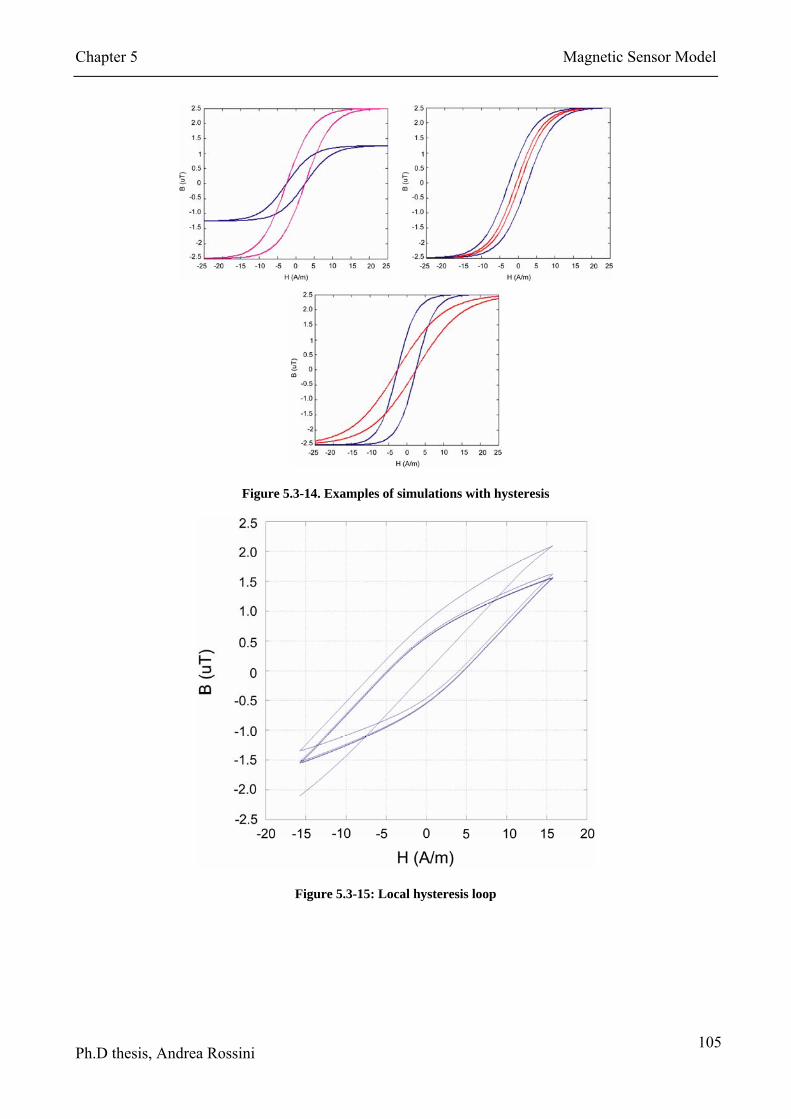
Chapter 5 Magnetic Sensor Model
Ph.D thesis, Andrea Rossini 105
Figure 5.3-14. Examples of simulations with hysteresis
Figure 5.3-15: Local hysteresis loop

Chapter 5 Magnetic Sensor Model
Ph.D thesis, Andrea Rossini 106
Figure 5.3-16: Complete hysteresis curve from the initial non magnetized condition to saturation
5.4 Experimental results
In order to validate the model, a magneto-inductance sensor has been emulated and compared with
a real device available commercially, shown in Figure 5.4-1. The circuit depicted in Figure 5.4-2
has been realized with discrete elements, where R1 = 13.5 kΩ, R3 = 100 kΩ, R4 = 4.7 kΩ, R5-8 =
0.2 kΩ, R9-12 = 100 Ω, 74AC08 element is a AND logic gate, 74HC4066 is a transmission gate
and TLC37021 is a LinCMOS micro-power voltage comparator, Figure 5.4-2.

Chapter 5 Magnetic Sensor Model
Ph.D thesis, Andrea Rossini 107
Figure 5.4-1: The PNI magneto-inductance sensor
Figure 5.4-2: The schematic of the circuit used with the magneto-inductance

Chapter 5 Magnetic Sensor Model
Ph.D thesis, Andrea Rossini 108
Figure 5.4-3: The PCB for the magneto-inductive sensor
To change the external magnetic field Helmholtz coils have been used. By means of a counter it has
been possible to determine the frequency and then the inductance of the sensor for the applied
magnetic field.
In
Figure 5.4-4 the measurement results obtained on the PNI sensor and the simulations results are
reported. Simulations results with and without the hysteresis introduced in the model are depicted.

Chapter 5 Magnetic Sensor Model
Ph.D thesis, Andrea Rossini 109
150
170
190
210
230
250
270
-800 -600 -400 -200 0 200 400 600 800
Magnetic Field [uT]
Freq
uenc
y [k
Hz]
=Experimental data Simulation with hysteresisSimulation without hysteresis
Figure 5.4-4: Comparison between the real sensor and the modelled one
It is possible to notice that in the case of the sensor model without hysteresis an error that is lower
than 10% compared with the real sensor has been obtained, while the error is lower than 5% with
the magnetic hysteresis enabled.
5.5 Conclusions
An Analog High-level Description Language (AHDL) model has been developed. The model has
been written in VERILOGA language for SPICE-like simulators.
The model describes the behaviour of four different types of sensors: a magneto-resistance, a
magneto-inductance, a hall device and a Fluxgate. The symbol of the magnetic sensor is a 5
terminal component, the meaning of some of the terminals can change depending on the type of
sensor. For all the models we have two main terminals, one of which is the reference, representing
the electrical output of the sensor, the other, the differential voltage across the main terminals or the
current through them is the effect of the magnetic field. A voltage generator or a current source
through a third terminal represents the input of the device: the external magnetic field, H. The

Chapter 5 Magnetic Sensor Model
Ph.D thesis, Andrea Rossini 110
remaining two terminals serve for the pick-up coil in Fluxgates or for monitoring internal quantities
for other sensors.
Performance depends on a number of parameters that are specified in the model card similarly to
what is done for active components. The global parameters for a given type of sensor are given in
the sensor model card, in which it is possible to set all the characteristic of the model, from the
physical dimension to the second order effect, like the temperature, the solder effect, the dispersed
field or the hysteresis.
The sensor has been compared with a real sensor to verify the correctness of the used equations.
The sensor show a very good match with the real one and a maximum error in the order of 10%
with the hysteresis disable, and 5% with the hysteresis enable.
The model is suitable to help the designers in the CADENCE environment providing the designers
with a tool that can simulate a real sensor behaviour. Indeed, the developed model has been
intensively used to design the Fluxgate magnetic sensor interface circuit described in Chapter 6.

Chapter 5 Magnetic Sensor Model
Ph.D thesis, Andrea Rossini 111

Chapter 6 Interface Circuit for Fluxgate Magnetic Sensor
Ph.D thesis, Andrea Rossini 112
Chapter 6
Interface Circuit for Fluxgate Magnetic Sensor
In this chapter an interface circuit for fluxgate magnetic sensors will be presented and discussed. In
particular, the circuit developed for the magnetic sensors, together with the simulation results and
the layout of the chip will be described. Finally, the experimental results and the measurement setup
will be shown.
6.1 The interface circuit design
The interface circuit presented in this chapter is suitable to supply and read-out a double axis micro
fluxgate magnetic sensor devoted to detect the Earth magnetic field.
The basic idea is to realize an interface circuit able to drive different types of fluxgate integrated
magnetic sensors with different characteristics. In particular, the dc resistance and excitation current
has to be taken into account as critical issues. The adopted solution has to allow a proper and smart
testing considering the instrumentation available nowadays and, in addition, it has to be cheap,
[33],.
The main advantages of an integrated solution are essentially related to its low power consumption
and small area occupation, without significant losses in performances. For this reason, the goal of
this project is to develop an integrated CMOS front-end circuit which guarantees the performance
required both in terms of noise and power consumption, in order to meet the requirements explained
above. The solution proposed will be useful not only for a System on Chip (SoC) or microsystem
solution, but also for a System on Package (SoP) or micromodule approach. Indeed, if the magnetic
sensor previously mentioned is realized in a separate die it is possible to bond together on the same
substrate the two dies. In this way the micromodule approach can be implemented, [34], [35].
It is worth to point out that, in the open literature, front-end circuits for fluxgate sensors are
typically based on a sinusoidal or pulsed excitation. By contrast, the approach followed in the
circuit discussed in this chapter uses a triangular current to feed the excitation coil and a
synchronous demodulation for reading-out the voltage induced in the sensing coils. This solution
represents a trade-off between the low-noise performance achieved by the solutions based on

Chapter 6 Interface Circuit for Fluxgate Magnetic Sensor
Ph.D thesis, Andrea Rossini 113
sinusoidal excitation and the simple implementation of solutions based on pulsed excitation, [36],
[37], [38].
Figure 6.1-1: Block diagram of the complete micro-system for magnetic field sensing
The block diagram of the entire micro-system is shown in Figure 6.1-1. The circuit is realized in a
standard 0.35-μm, 2 poly, 4 metal levels, high resistivity polysilicon CMOS process with high
voltage module (25-V devices).
The sensor,[28] used to test the front-end circuit, has been realized in a 0.5-μm CMOS technology
with a post processing step for the ferromagnetic material deposition which includes copper metal
lines for the excitation coil and aluminium metal lines for the sensing coils. The total area of the
planar copper excitation coil (5.5 µm thickness, 71 turns and 12 µm pitch (8 µm metal width and 4
µm of spacing between two metals) is 1760 x 1760 µm2 and its resistance is about of 123.4 Ω. The
total area for the aluminium sensing coils (1 µm thickness, 66 turns, 3 µm pitch 1.4 µm metal width
and 1.6 µm of spacing between two metals) is 650 x 650 µm2 and their resistance is about 1.84 kΩ.
A photograph of the sensor chip is shown in Figure 6.1-2.

Chapter 6 Interface Circuit for Fluxgate Magnetic Sensor
Ph.D thesis, Andrea Rossini 114
Figure 6.1-2: Microphotography the sensor chip
The front-end circuit can be divided into four main blocks: the timing block, the excitation block,
the read-out unit and the ADC converter.
6.1.1 Timing Block
In order to ensure proper timing for the excitation and read-out blocks, the whole circuit is driven
by a clock at 400 kHz. This clock is internally divided, by a cascade of flip-flops.
The outputs of this timing block are two signals: a 100 kHz square wave signal with its
complementary output, that is used to drive the excitation block, and a 200 kHz square wave signal,

Chapter 6 Interface Circuit for Fluxgate Magnetic Sensor
Ph.D thesis, Andrea Rossini 115
used to drive the read-out block and to realize the second harmonic demodulation, needed to
measure the sensor output. By using a 400 kHz master clock a duty cycle of 50% on both the 100
kHz and the 200 kHz output waveforms can be ensured. A duty cycle different from 50%, indeed,
could compromise the demodulation of the signals produced by the sensing coils and, therefore, it
has to be avoided.
6.1.2 Excitation Block
To periodically saturate the ferromagnetic material deposited over the excitation coil of the planar
fluxgate sensor a triangular current waveform has been used, as shown in Figure 5.2-8. The
excitation circuit consists of two different blocks, with two different power supplies values: the first
is a low voltage block, with a power supply equal to 3.3 V, while the second, realized by employing
high-voltage transistors, uses a power supply as high as 25 V. The first block generates a square
wave with frequency equal to 100 kHz. Moreover, in order to guarantee the programmability of the
system and, hence, the possibility to use it with different kinds of sensors and magnetic materials,
the input of the integrator in not fixed. In this way it is possible to modify the output current,
according to the sensor characteristics and the power consumption requirements. This current is
then integrated, with a two stage amplifier with a capacitor in the feedback loop, in order to obtain a
triangular waveform centered around half of the low power supply. Indeed, an higher excitation
current improves the saturation of the ferromagnetic materials, thus allowing achieving better
results in terms of noise and sensitivity, but with higher power consumption.
The second block, depicted in Figure 6.1-3, consists of an high voltage mirrored operational
amplifier with low-impedance output stage, which receives the triangular waveform at the input
and, by means of a resistive feedback loop (not shown in figure), produces a triangular current at its
output. The mirrored amplifier allows achieving the maximum swing at the output terminal. The
class-AB amplifier output stage is designed to provide all the current required by the sensor. A
decoupling stage between the low-voltage and the high-voltage blocks is necessary to level shift the
triangular wave produced by the low-voltage block around half of the high power supply voltage.

Chapter 6 Interface Circuit for Fluxgate Magnetic Sensor
Ph.D thesis, Andrea Rossini 116
Figure 6.1-3: High voltage mirrored amplifier
The behaviour of the excitation block is the following: for half of the clock period the integrator
input is connected to Vin, while in the other half to –Vin, changing the slope of the triangular wave at
the voltage integrator output. This voltage feeds the trans-conductance amplifier. The peak output
current can be regulated by trimming the value of Vin, according to:
1
1
1 t T
out intV V dt
RC+
= − ∫i i (6.1)
The chip has to work with different sensors with different resistance of the excitation coils, varying
from several tens to few hundreds of Ohm. The highest resistance of the integrated coil (estimated
around 280 Ω) and the possibility to test the sensor with an excitation current higher than ±15 mA
(e.g. ±20 mA or higher) could produce a 6-V output swing. For this reason, the output stage of the
tranconductance amplifier has been supplied with 25 V (HV) and, hence, the use of high voltage
transistors has been required. In addition, in this way, it is possible to separate the power
consumption of the two structures, supplying with high voltage only the power stage and, hence,
reducing the power consumption in the integrator and the amplifiers.
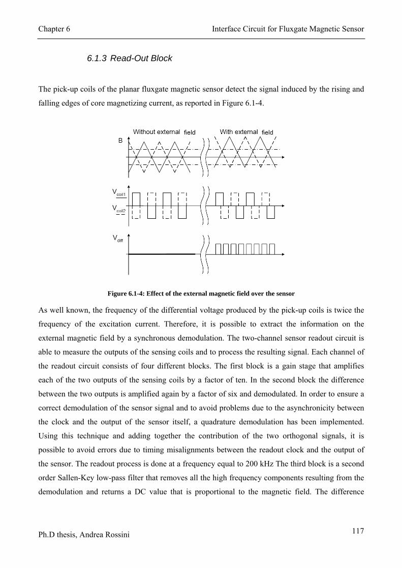
Chapter 6 Interface Circuit for Fluxgate Magnetic Sensor
Ph.D thesis, Andrea Rossini 117
6.1.3 Read-Out Block
The pick-up coils of the planar fluxgate magnetic sensor detect the signal induced by the rising and
falling edges of core magnetizing current, as reported in Figure 6.1-4.
Figure 6.1-4: Effect of the external magnetic field over the sensor
As well known, the frequency of the differential voltage produced by the pick-up coils is twice the
frequency of the excitation current. Therefore, it is possible to extract the information on the
external magnetic field by a synchronous demodulation. The two-channel sensor readout circuit is
able to measure the outputs of the sensing coils and to process the resulting signal. Each channel of
the readout circuit consists of four different blocks. The first block is a gain stage that amplifies
each of the two outputs of the sensing coils by a factor of ten. In the second block the difference
between the two outputs is amplified again by a factor of six and demodulated. In order to ensure a
correct demodulation of the sensor signal and to avoid problems due to the asynchronicity between
the clock and the output of the sensor itself, a quadrature demodulation has been implemented.
Using this technique and adding together the contribution of the two orthogonal signals, it is
possible to avoid errors due to timing misalignments between the readout clock and the output of
the sensor. The readout process is done at a frequency equal to 200 kHz The third block is a second
order Sallen-Key low-pass filter that removes all the high frequency components resulting from the
demodulation and returns a DC value that is proportional to the magnetic field. The difference

Chapter 6 Interface Circuit for Fluxgate Magnetic Sensor
Ph.D thesis, Andrea Rossini 118
between this output and the analog ground is then amplified with programmable gain (from 0 to
100) in the last block.
6.1.4 The ADC
The DC output of the readout chain is finally processed by a 13-bit ADC and delivered in digital
form to the output. A single ADC with a multiplexer for both readout channels has been used. With
the switched-capacitor oversampled 13-bit incremental A/D converter available in the library, it is
possible to have a resolution equal to 13 bit in a range of 1 V centred at 1.65 V, giving a least
significant bit (LSB) equal to 122 μV. This range is flexible and can be adjusted according to the
output of the read-out circuitry. The A/D converter operates at a nominal sampling frequency of 1
MHz providing a full resolution conversion in 8 ms with a power consumption of 950 μW. Thus the
nominal system read-out rate is 100 Hz.
6.2 Simulation Results
The proposed system has been simulated in order to evaluate the overall performance. For this
purpose we have first used, for the excitation block and the readout block, the magnetic model
described in the previous chapter, in order to obtain a good approximation with the real resistance
value of the excitation coils of the actual sensor that loads the excitation circuit.
Then a real signal obtained from the oscilloscope while measuring the actual sensor has been used
as input signal for the readout circuit in Cadence environment for the simulation. The actual input
signal, indeed, shows some non-idealities in the output of the sensors that are not easily
reproducible with an ideal source. The actual signal has been saved in a text file and then used in
Cadence with a specific routine, as shown in Figure 6.2-1. In particular it is possible to notice the
presence of a square waveform superimposed on top of the useful signal, due to a capacitive
coupling between the excitation and the sensing coils. Moreover, it is possible to observe that the
differential sensor signal near the positive or negative edges is very small if compared with the
common-mode noise. Thanks to the difference between the two sensor signals performed inside the
interface circuit, it is possible to eliminate the common mode noise and amplify only the signal
proportional to magnetic field.

Chapter 6 Interface Circuit for Fluxgate Magnetic Sensor
Ph.D thesis, Andrea Rossini 119
Figure 6.2-2 shows the triangular current with the maximum amplitude allowed by the class-AB
push-pull high-voltage output stage, equal to 22 mA, in the case of a resistance for the excitation
coil of about 280 Ω.
The interface circuit has been simulated with different input signals, chosen on the basis of the
signal obtained from the oscilloscope, as shown in Figure 6.2-3. This signal has been modelled for
simplicity as a square wave with the signal superimposed not at the edge but at the centre of the
positive or negative value. The different output signals (Figure 6.2-4) obtained have been used to
evaluate the linearity of the whole readout system with different values of the overall gain. The
linearity error obtained is lower than 1% of the full scale (1.05 V to 2.15 V at the input of A/D
converter). The maximum swing of the circuit ranges between 0.4 V and 2.9 V and is tuneable by
setting the gain of the readout chain, according to the sensor sensitivity.
Figure 6.2-1:Sensor signal from the oscilloscope
Figure 6.2-2: Output current of the excitation block

Chapter 6 Interface Circuit for Fluxgate Magnetic Sensor
Ph.D thesis, Andrea Rossini 120
Figure 6.2-3: Different input signals
Figure 6.2-4: Simulated output swing of the chip
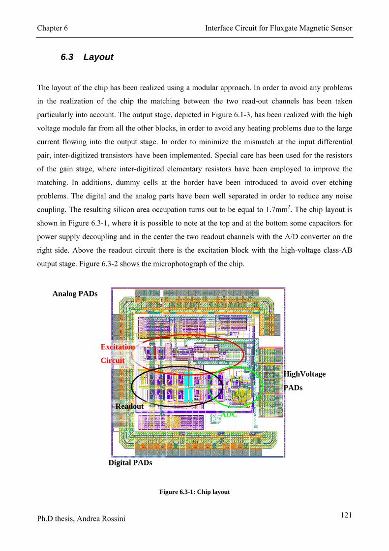
Chapter 6 Interface Circuit for Fluxgate Magnetic Sensor
Ph.D thesis, Andrea Rossini 121
6.3 Layout
The layout of the chip has been realized using a modular approach. In order to avoid any problems
in the realization of the chip the matching between the two read-out channels has been taken
particularly into account. The output stage, depicted in Figure 6.1-3, has been realized with the high
voltage module far from all the other blocks, in order to avoid any heating problems due to the large
current flowing into the output stage. In order to minimize the mismatch at the input differential
pair, inter-digitized transistors have been implemented. Special care has been used for the resistors
of the gain stage, where inter-digitized elementary resistors have been employed to improve the
matching. In additions, dummy cells at the border have been introduced to avoid over etching
problems. The digital and the analog parts have been well separated in order to reduce any noise
coupling. The resulting silicon area occupation turns out to be equal to 1.7mm2. The chip layout is
shown in Figure 6.3-1, where it is possible to note at the top and at the bottom some capacitors for
power supply decoupling and in the center the two readout channels with the A/D converter on the
right side. Above the readout circuit there is the excitation block with the high-voltage class-AB
output stage. Figure 6.3-2 shows the microphotograph of the chip.
Figure 6.3-1: Chip layout
Readout ADC
Digital PADs
HighVoltage
PADs
Analog PADs
Excitation
Circuit

Chapter 6 Interface Circuit for Fluxgate Magnetic Sensor
Ph.D thesis, Andrea Rossini 122
Figure 6.3-2: Microphotography of the Read-Out chip
6.4 Experimental results
A custom Printed Circuit Board (PCB) has been realized in order to allow the characterization of
the chip. By using the custom PCB, shown in Figure 6.4-1, it is possible to correctly provide biasing
and power supply voltages to the chip. Furthermore, by employing a logic analyzer, it is possible to
evaluate the digital output of the ADC, in the board we reserved space for the sensor wide apart
from the copper layer in order to allow a correct read-out of the signal inside the Helmhtoz coils.
The measurements performed concern the linearity of the acquisition channel and the correct
reconstruction of the rotation angle of the chip referred to the north-south direction. The
measurements obtained have been compared with the previous results of the stand-alone sensor.
Using a HP spectrum analyzer and a function generator and applying directly a triangular excitation
current with a peak of 18 mA at 100 kHz, the stand-alone sensor shows a magnetic sensitivity of
about 0.45 mV/µT, suitable for detecting the Earth’s magnetic field (±50 µT), while the linearity
error is 1.15% of the full scale. The maximum angle error, when combining the measurements of
the X and Y components of the Earth magnetic field, is 3.4°.
The chip linearity has been first evaluated by using the Helmholtz coils.

Chapter 6 Interface Circuit for Fluxgate Magnetic Sensor
Ph.D thesis, Andrea Rossini 123
Figure 6.4-1: Printed circuit board for the chip
Varying the current flowing into the Helmholtz coils it is possible to generate an external field with
a well-know value. If the sensor is oriented in a direction parallel to this field and perpendicularly to
the Earth’s magnetic field, then it is possible to evaluate only the effect of the external field and
obtain a characterization of the device itself. Figure 6.4-2 shows the output of the ADC from the
negative to the positive saturation as a function of the external magnetic field applied with the
Helmholtz coils, while Figure 6.4-3 shows a zoom in the earth magnetic field zone.
Space for
sensor

Chapter 6 Interface Circuit for Fluxgate Magnetic Sensor
Ph.D thesis, Andrea Rossini 124
Figure 6.4-2: Digital output of the sensor as a function of the magnetic field generated from saturation to
saturation
Figure 6.4-3: Digital output of the interface circuit as a function of the applied magnetic induction in the Earth
field range

Chapter 6 Interface Circuit for Fluxgate Magnetic Sensor
Ph.D thesis, Andrea Rossini 125
The system response is linear in the range of ±60 µT, with a maximum non-linearity error of about
3% of the full-scale from the ideal fit, as shown in Figure 6.4-4. The sensitivity obtained is 11
LSB/µT, where 1 LSB is equal to 125 µV.
Figure 6.4-4: Linearity error as a function of the applied magnetic induction
In order to evaluate the performance of the micro-fluxgate sensing system as a compass, the device
has been rotated in an horizontal plane, while exposing it to the Earth magnetic field. Figure 6.4-5
shows the digital output of the two axes of sensitivity as a function of rotation angle. The angle
error is smaller than 4° and includes signal non-linearity, hysteresis and noise, as well as the
inaccuracy of the setup.
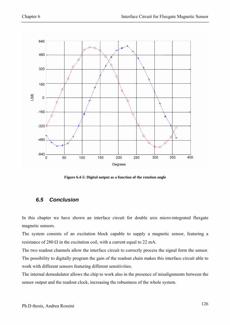
Chapter 6 Interface Circuit for Fluxgate Magnetic Sensor
Ph.D thesis, Andrea Rossini 126
Figure 6.4-5: Digital output as a function of the rotation angle
6.5 Conclusion
In this chapter we have shown an interface circuit for double axis micro-integrated fluxgate
magnetic sensors.
The system consists of an excitation block capable to supply a magnetic sensor, featuring a
resistance of 280 Ω in the excitation coil, with a current equal to 22 mA.
The two readout channels allow the interface circuit to correctly process the signal form the sensor.
The possibility to digitally program the gain of the readout chain makes this interface circuit able to
work with different sensors featuring different sensitivities.
The internal demodulator allows the chip to work also in the presence of misalignments between the
sensor output and the readout clock, increasing the robustness of the whole system.

Chapter 6 Interface Circuit for Fluxgate Magnetic Sensor
Ph.D thesis, Andrea Rossini 127
The most important features of the device are summarized in Features of the proposed chipTable
6.1.
Parameter Value
Sensor technology 0.5 µm CMOS
Ferromagnetic core Vitrovac 6025 X deposited by DC-magnetron
sputtering
Interface circuit technology 0.35 µm CMOS
Sensor area 3.2 mm2
Interface circuit area 1.7 mm2
Supply voltage 3.3 V–26 V
Magnetic field range ±60 µT
Linearity error 3% of full scale
Angle error (Earth magnetic field) 4°
Table 6.1: Features of the proposed chip
The application areas for the developed micro-sensor interface circuit are wide. Good sensitivity,
small dimensions and low power consumption from low power supply voltage make it interesting
for portable applications where it is possible to interface the circuit directly to the digital domain.
These applications include:
• Electronic compass;
• Magnetic field detection for medical applications;
• Current measurement;
• Vehicle recognition and other.

Chapter 6 Interface Circuit for Fluxgate Magnetic Sensor
Ph.D thesis, Andrea Rossini 128

127
Conclusions In this thesis we have presented a Wilkinson A/D converter able to resolve 10 bit. The main
characteristic of the converter are:
• INL lower than ±0.5 LSB;
• DNL lower than ±0.6 LSB;
• Clock frequency 50 MHz;
• Input range 1.2 V centered around 1.5 V;
The basic block of the Wilkinson converter are: an input buffer, a comparator, an output register, a
ramp generator, a counter and a clock generator.
For every channel of the pixel matrix there is available one Wilkinson converter, so special care has
been taken in order to limit the power consumption of the whole chip. Since the Wilkinson
converter will not serve only one pixel but sixteen it is possible to slightly increase the current of
the converter without worst the power budget.
The converter has been measured to evaluate the linearity inside the acquisition chain, obtaining a
total DNL and INL lower than ±0.2LSB and ±3.3LSB with a resolution equal to 10bit.
The offset and gain spread between the different channels show no substantial differences, that
suggests that their variation between channels have a negligible effect with request to the variation
within the RPCs..
The power consumption of all the chain is estimated in 0.9mW while the one of the converter stand
alone is about 0.4mW.
A 10 bit pipeline without clock for X-ray spectrometry is presented. The converter is able to convert
an input signal in 2.5μs and achieves 8 bit of resolution. The structure consist of 9 1.5 bit for cell
and a final flash of 2 bit. The structure acts like a combination logic, where the second stage starts
to convert the output of the first stage before that the output itself is stable, and the same also for the
third stage and so on. A SOC/EOC generator is needed to indicate when the conversion is finished.
The total characteristics of the converter are reassumed in the following outline:
• Power consumption 95mW ([email protected] )
• DNL ± 1.2LSB
• INL ± 2.5LSB
• SNR 55.4 dB
• Conversion time 2.50μs

128
An Analog High-level Description Language (AHDL) model has been developed. The model has
been written in VERILOGA language for SPICE-like simulators.
The model describes the behaviour of four different types of sensors: a magneto-resistance, a
magneto-inductance, a hall device and a fluxgate. The symbol of the magnetic sensor is a 5 terminal
component, the meaning of some of the terminals can change depending on the type of sensor. For
all the models we have two main terminals, one of which is the reference, representing the electrical
output of the sensor. Thus, the differential voltage across the main terminals or the current through
them is the effect of the magnetic field. A voltage generator or a current source through a third
terminal represents the input of the device: the external magnetic field, H. The remaining two
terminals serve for the pick-up coil in flux-gates or for monitoring internal quantities for other
sensors.
Performance depends on a number of parameters that are specified in the model card similarly to
what is done for active components. The global parameters for a given type of sensor are given in
the sensor model card, in which it is possible to set all the characteristic of the model, from the
physical dimension to the second order effect, like the temperature, the solder effect, the dispersed
field or the hysteresis.
The sensor has been compared with a real sensor to verify the correctness of the used equations.
The sensor show a maximum error in the order of 10% with the hysteresis disable, and 5% with the
hysteresis enable.
The model is suitable to help the designers in the CADENCE environment providing the designers
with a tool that can simulate a real sensor behavior. In this chapter we have shown an interface
circuit for double axis micro-integrated fluxgate magnetic sensors.
The system consists of an excitation block capable to supply a magnetic sensor, featuring a
resistance of 280 Ω in the excitation coil, with a current equal to 22 mA.
The two readout channels allow the interface circuit to correctly process the signal form the sensor.
The possibility to digitally program the gain of the readout chain makes this interface circuit able to
work with different sensors featuring different sensitivities.
The internal demodulator allows the chip to work also in the presence of misalignments between the
sensor output and the readout clock, increasing the robustness of the whole system.
The most important features of the device are summarized in Errore. L'origine riferimento non è
stata trovata.Errore. L'origine riferimento non è stata trovata..
The application areas for the developed micro-sensor interface circuit are wide. Good sensitivity,
small dimensions and low power consumption from low power supply voltage make it interesting

129
for portable applications where it is possible to interface the circuit directly to the digital domain.
These applications include:
• Electronic compass;
• Magnetic field detection for medical applications;
• Current measurement;
• Vehicle recognition and other.

130

129
Bibliography
1. Hall Effect sensing and application, Honeywell tutorial book, available at www.honeywell.com
2. Technology-Driven Alternatives for Smart Sensor Interfaces, A. Baschirotto and P. Malcovati,
chapter 4
3. An Introduction to Classical Electromagnetic Radiation, Gleen Smith, Cambridge press,1997
4. Scintillation light read-out by low-gain thin avalanche photodiodes in silicon wells Allier, C.P.;
Hollander, R.W.; Sarro, P.M.; de Boer, M.; van Eijk, C.W.E. Nuclear Science, IEEE
Transactions on, Vol.47, Iss.4, Aug 2000, Pages:1303-1306;
5. CsI(Tl)-photodiode detectors for γ-ray spectroscopy, Fioretto, E.; Innocenti, F.; Viesti, G.;
Cinausero, M.; Zuin, L.; Fabris, D.; Lunardon, M.; Nebbia, G.; Prete, G., Nuclear Science,
IEEE Transactions on, Vol.47, Iss.4, Aug 2000, Pages:1315-131;
6. A 16 channel analogue sparse readout I.C. for INTEGRAL (International Gamma-Ray
Astrophysics Laboratory); Prydderch, M.L.; Seller, P. Nuclear Science, IEEE Transactions on,
Vol.42, Iss.4, Aug 1995, Pages:776-780;
7. A Double Polarity CMOS Peak and Hold Circuit for Satellite Radiation Detection System;
F. Borghetti, R. Magni, P. Malcovati, A. Rossini, ISCAS 2005, Kobe Japan,23 May-26 May
2005;
8. ICARUS ASIC: a 16 channel photodiode read out system, Labanti, C.; Rossi, E.; Mauri, A.;
Bastia, P.; Foglia, L.; Krummenacher, F.; Valence, V., Nuclear Science, IEEE Transactions on,
Vol.46, Iss.3, Jun 1999, Pages:144-149;
9. The Imager on Board INTEGRAL; P. Ubertini et al., SPIE Vol 2806, pag 246, 1996;
10. ICARUS ASIC: a 16 channel photodiode read out system; Labanti, C.; Rossi, E.; Mauri, A.;
Rastia, P.; Foglia, L.; Krummenacher, F.; Valence, V., Nuclear Science Symposium, 1998.
Conference Record. 1998 IEEE, Vol.1, Iss., 1998, Pages:428-433 vol.1
11. CMOS Preamplifier with High Linearity and Ultra Low Noise for X-Ray Spectroscopy;
P. O’Connor, G. Gramegna, P. Rehak, F. Corsi, C. Marzocca; Nuclear Science, IEEE
Transactions on; Vol. 44 Pages 318-325;
12. Current Mirror Reset for Low-Power BiCMOS Charge Amplifiers; M. Sampietro, G. Bertuccio,
L. Fasoli; Nuclear Instrumentation and Method; A439 Pages 447-450 2000;

130
13. An Integrated Reset/Pile-up Rejector Circuit for Pixel Readout ASIC's; P. Bastia, G. Bertuccio,
F. Borghetti, S. Caccia, V. Ferragina, F. Ferrari, D. Maiocchi, P. Malcovati, D. Martin,
A. Pullia, N. Ratti; Submetted to to Nuclear Science Symposium 2004;
14. A multi-channel ADC for use in the PHENIX detector; Emery, M.S.; Frank, S.S.; Britton, C.L.,
Jr.; Wintenberg, A.L.; Simpson, M.L.; Ericson, M.N.; Young, G.R.; Clonts, L.G.; Allen, M.D.;
Nuclear Science, IEEE Transactions on, Vol.44, Iss.3, Jun 1997; Pages:374-378
15. Implementation of a Novel Read-Out Strategy Based on a Wilkinson ADC for a 16x16 Pixel X-
Ray Detector Array; V. Ferragina, P. Malcovati, F. Borghetti, A. Rossini, N. Ratti, F. Ferrari, G.
Bertuccio; submitted to ISCAS ’05;
16. Proceeding of the 11th International Workshop on Room Temperature Semiconductor X and
Gamma Ray Detectors and Associated Electronics, in R. James, P. Siffert ed., Nuclear
Instruments and Methods A, vol. 458, Elsevier Science, 2001.
17. M. Prydderch, P. Seller, “A 16 channel analogue sparse readout IC for Integral”, IEEE Nucl.
Sc. Symp. And Med. Imag. Conf., 1 , pp. 65-68, 1994.
18. R. van de Plassche, Integrated Analog to Digital and Digital to Analog Converters, 2nd ed.,
Kluwer 2003
19. Progetto di un convertitore A/D pipeline senza clock per la catena di acquisizione di uno
spettrometro a raggi x, Luca Picolli, Thesis degree, 2004
20. Gain error correction scheme for multiply-by-two gain amplifier in pipelined ADC; Lee, Y.P.;
Geiger, R.L.; Circuits and Systems, 1999. 42nd Midwest Symposium on, Vol.1, Iss., 1999;
Pages:190-193 vol. 1;
21. Digital error correction and calibration of gain non-linearities in a pipelined ADC; Ravindran,
A.; Savia, A.; Leonard, J.; Circuits and Systems, 2004. ISCAS '04. Proceedings of the 2004
International Symposium on, Vol.1, Iss., 23-26 May 2004; Pages: I-1- I-4 Vol.1
22. A pipelined A/D converter for high-speed and high-resolution application; Runhua Sun; Lihua
Peng; Circuits and Systems, 2002. ISCAS 2002. IEEE International Symposium on, Vol.1, Iss.,
2002; Pages: I-917- I-920 vol.1
23. Improvements of CMOS Hall Microsystems and Application for Absolute Angular Position
Measurements, Michel Demierre thesis, Ecole Politecnique Federal de Lausanne
24. Behavioral Model of Magnetic Sensors for SPICE Simulations,A. Rossini, F. Borghetti, P.
Malcovati, F. Maloberti, ICECS 2005, Gammart Tunisi, December 11-14th 2005

131
25. Magnetoresistance (MR) Transducers And How to Use Them as Sensors, Perry A. Holman,
Ph.D., Honeywell International Inc., July 2004 available at www.honeywell.com
26. General Appendices, File under Discrete Semiconductors, SC17,1997 Jan 09, Philips
semiconductors, available at www.philips.com
27. Electronic compass using two-axis micro fluxgate sensing element, Hwang, J.-S.; Parket
others.;TRANSDUCERS, Solid-State Sensors, Actuators and Microsystems, 12th International
Conference on, 8-12 June 2003 Page(s):1618 - 1621 vol.2
28. Fluxgate Magnetic Sensor System for Electronic Compass Marco Marchesi, Ph.D thesis,
University of Pavia, Pavia, 2005
29. PNI SEN-S65 Magneto-Inductive Sensor 1000619 R04 - March 2004, available at
www.pnicorp.com
30. PNI V2Xe 2-Axis Compass Module, 1000883 R03 - January 2004, available at
www.pnicorp.com
31. Mathematical model for hysteresis, Physical review letter, I.D. Mayergoyz vol.56 n15, 14 april
1986
32. Limiting Loop Proximity Hysteresis Model, Luiz Alberto Luz de Almeida et others, IEEE
TRANSACTIONS ON MAGNETICS, VOL. 39, NO. 1, JANUARY 2003
33. S. Kawahito, A. Cerman, K. Aramaki, and Y. Tadokoro, “A weak magnetic field measurement
system using micro-fluxgate sensors and delta-sigma interface,” IEEE Trans. Instrum. Meas.,
vol. 52, no. 1, pp. 103–110, Feb. 2003.
34. Predrag M. Drljaca, Pavel Kejik, Franck Vincent, Dominique Piguet, and Radivoje S. Popovic,
“Low-Power 2D Fully Integrated CMOS Fluxgate Magnetometer”, IEEE Sensors Journal
(2005).
35. A. Rossini et other “A CMOS 2D Micro-Fluxgate Earth Magnetic Field Sensor with Digital
Output” ISSCC 2007,10-15 febbruary 2007, san Francisco California
36. A. Baschirotto, E. Dallago, P. Malcovati, M. Marchesi, G. Venchi, “From a PCB Fluxgate to an
integrated micro Fluxgate magnetic sensor“, Proceeding of Instrumentation and Measurement
Technology Conference (IMTC-2005), Ottawa (Canada) 17 – 19 May 2005, pp. 1756-1760.
37. P. Ripka, San On Choi; A. Tipek, S. Kawahito, M. Ishida, “Pulse excitation of microfluxgate
sensors”, IEEE Transactions on Magnetics, Vol.37, N. 4, pp. 1998-2000, 2001.

132
38. A. Baschirotto, F. Borghetti, E. Dallago, P. Malcovati, M. Marchesi, E. Melissano, P.Siciliano,
G. Venchi, “Fluxgate magnetic sensor and front-end circuitry in a microintegrated system”,
Proceedings of EUROSENSORS, Barcellona 11-14 September 2005,pp. WPb42, 2005.
39. Wilkinson A/D Converter for X-Ray Detectors for Space Applications. A. Rossini, F. Borghetti,
P. Malcovati, G. Bertuccio, N. Ratti, I. Cappelletti , 20th EUROSENSORS conference
GÖTEBORG, SWEDEN 17th-20th september

133

Acknowledgments/Ringraziamenti
Ph.D thesis, Andrea Rossini
134
Acknowledgments/Ringraziamenti Dopo questo lavoro di tesi, desidero ringraziare le persone che hanno reso possibile questa
esperienza, prima di tutto il Prof. Piero Malcovati e il Prof Franco Maloberti, per avermi dato la
possibilità di lavorare nel loro laboratorio ed avermi aiutato ogni volta che ne avevo bisogno, la loro
competenza e professionalità mi è stata di grande aiuto in questi tre anni di dottorato. Un grazie va
rivolto anche al Prof. Andrea Baschirotto, anche in lui ho trovato un valido e prezioso aiuto. Oltre
alla professionalità e alla competenza con queste persone si è instaurato anche un rapporto di stima e
amicizia che spero vivamente continuerà anche fuori dall’ambito universitario.
Ringrazio anche il prof. Enrico Dallago con cui ho collaborato nell’ultimo anno di attività, e il prof.
Guido Torelli con cui invece ho lavorato il primo anno e i loro rispettivi team.
Desidero ringraziare poi tutte le persone del laboratorio di microsistemi integrati con cui ho
condiviso questi anni di studio/lavoro/divertimento, dai dottorandi anziani quando ero io un
dottorando giovane, ai dottorandi giovani quando ero io quello anziano. Ringrazio anche gli amici
degli altri laboratori, quelli incontrati e conosciuti alle conferenze, o semplicemente in giro. Tra tutti
Fausto (il maestro), Ivan (l’aiutante), Paolo (Paolissimo), Cristina (team digitale e analogico
assieme), Luca (il Picoz), Max (Svezia) e Max (dali), Roberto (www.zampironi.org), Marco
(l’uomo magnetico), Edo (arredo), Ale (carbons) e Ale (il vero Ale…).
Desidero ringraziare gli amici della compagnia di Mede, Ottobiano, Pavia e Garlasco, teo (il Teo),
Marco con cui ho condiviso parte dell’esperienza in Olanda e Andrea suo cugino per i suoi preziosi
consigli/conoscenza della geografia europea, Trama e Aleandro(il pilota), Paolo per le tantissime
domeniche al mare, Giacomo (vendimi la tua casa al mare) e Fra (magicosnafuz).
Ovviamente gli altri non si sentano esclusi se non li ho citati direttamente, la lista diventerebbe
troppo lunga. Ringrazio tutti vivamente e di cuore.
Infine dedico il mio lavoro di tesi e ringrazio i miei genitori e le mie sorelle. Il motivo è sempre il
solito: hanno sempre creduto in me anche quando non ci credevo io. Mi hanno sempre aiutato e
spronato quando volevo smettere e mi hanno dato la forza di andare avanti nonostante tutto quello
che è successo. Se non fosse per voi, non starei scrivendo queste righe. GRAZIE!!

Acknowledgments/Ringraziamenti
Ph.D thesis, Andrea Rossini
135