Embed Size (px)
Citation preview

1
EECS 373 Design of Microprocessor-Based Systems Ronald Dreslinski University of Michigan Lecture 14: Memory and Peripheral Busses
PCB design/terminology
Slides developed in part by Prof. Dutta & Brehob

Administrative
• Milestone Meeting 1 – Thur/Friday of this week
• Group Lecture Presentations – Details on Thursday – Start on Mar. 22nd
• No Lecture Next Tuesday (3/20) – Work on projects
2

Outline
• Memory review
• AHB bus
• PCB material
3

Memory basics
• Read only
• Volatile – Dynamic
• Wearout
• Latencies
4

Memory array types
5
Memory Arrays
Random Access Memory Serial Access Memory Content Addressable Memory(CAM)
Read/Write Memory(RAM)
(Volatile)
Read Only Memory(ROM)
(Nonvolatile)
Static RAM(SRAM)
Dynamic RAM(DRAM)
Shift Registers Queues
First InFirst Out(FIFO)
Last InFirst Out(LIFO)
Serial InParallel Out
(SIPO)
Parallel InSerial Out
(PISO)
Mask ROM ProgrammableROM
(PROM)
ErasableProgrammable
ROM(EPROM)
ElectricallyErasable
ProgrammableROM
(EEPROM)
Flash ROM

• Ferroelectric RAM
• Phase change memory
• Magnetoreseistive RAM
• Programmable metallization cell
6

Outline
• Memory review
• AHB-Lite bus
• Start on PCB material (time allowing)
7

Modern embedded systems have multiple busses
8
Atmel SAM3U
Today

Advanced Microcontroller Bus Architecture (AMBA) - Advanced High-performance Bus (AHB) - Advanced Peripheral Bus (APB)
AHB • High performance • Pipelined operation • Burst transfers • Multiple bus masters • Split transactions
APB • Low power • Latched address/control • Simple interface • Suitable of many
peripherals
9
10
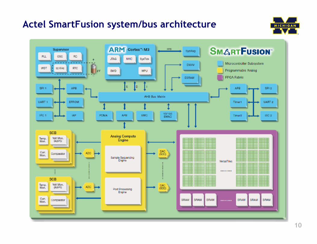
Actel SmartFusion system/bus architecture

11
AHB-Lite supports single bus master and provides high-bandwidth operation
• Burst transfers
• Single clock-edge operation
• Non-tri-state implementation like APB
• Configurable bus width
Most figures in this section from AMBA 3 AHB-Lite Protocol v1.0 You have to register with ARM (trivial) for this, we can’t post it.

12
AHB-Lite bus master/slave interface
• Global signals – HCLK – HRESETn
• Master out/slave in – HADDR (address) – HWDATA (write data) – Control
• HWRITE • HSIZE • HBURST • HPROT • HTRANS • HMASTLOCK
• Slave out/master in – HRDATA (read data) – HREADY – HRESP
13
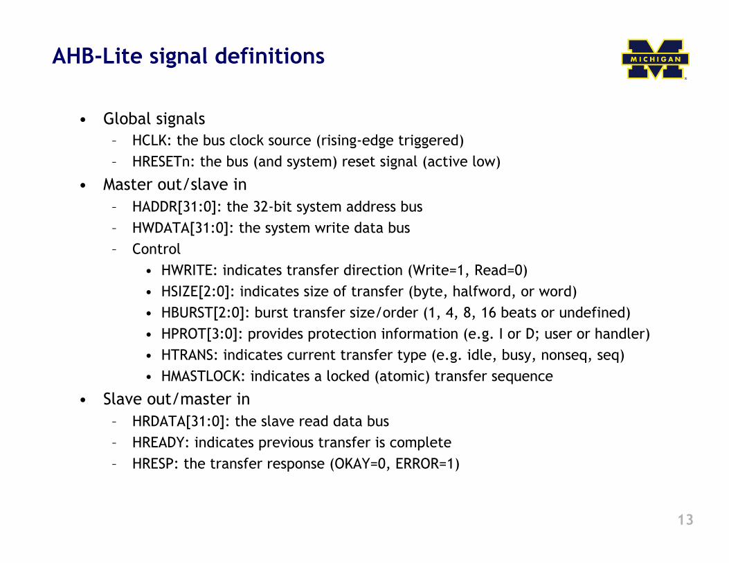
AHB-Lite signal definitions
• Global signals – HCLK: the bus clock source (rising-edge triggered) – HRESETn: the bus (and system) reset signal (active low)
• Master out/slave in – HADDR[31:0]: the 32-bit system address bus – HWDATA[31:0]: the system write data bus – Control
• HWRITE: indicates transfer direction (Write=1, Read=0) • HSIZE[2:0]: indicates size of transfer (byte, halfword, or word) • HBURST[2:0]: burst transfer size/order (1, 4, 8, 16 beats or undefined) • HPROT[3:0]: provides protection information (e.g. I or D; user or handler) • HTRANS: indicates current transfer type (e.g. idle, busy, nonseq, seq) • HMASTLOCK: indicates a locked (atomic) transfer sequence
• Slave out/master in – HRDATA[31:0]: the slave read data bus – HREADY: indicates previous transfer is complete – HRESP: the transfer response (OKAY=0, ERROR=1)

14
Key to timing diagram conventions (As APB)
• Timing diagrams – Clock – Stable values – Transitions – High-impedance
• Signal conventions – Lower case ‘n’ denote
active low (e.g. RESETn) – Prefix ‘H’ denotes AHB – Prefix ‘P’ denotes APB

15
Basic read and write transfers with no wait states
Pipelined Address & Data Transfer

16
Read transfer with two wait states
Two wait states added by slave by asserting HREADY low
Valid data produced
17
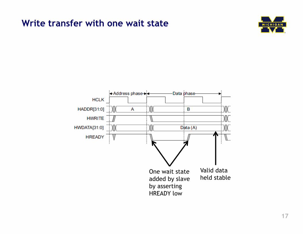
Write transfer with one wait state
One wait state added by slave by asserting HREADY low
Valid data held stable

18
Wait states extend the address phase of next transfer
One wait state added by slave by asserting HREADY low
Address stage of the next transfer is also extended

19
Transfers can be of four types (HTRANS[1:0])
• IDLE (b00) – No data transfer is required – Slave must OKAY w/o waiting – Slave must ignore IDLE
• BUSY (b01) – Master inserts idle cycles in a burst (wait states) – Burst will continue afterward – Address/control reflects next transfer in burst – Slave must OKAY w/o waiting – Slave must ignore BUSY
• NONSEQ (b10) – Indicates single transfer or first transfer of a burst – Address/control unrelated to prior transfers
• SEQ (b11) – Remaining transfers in a burst – Addr = prior addr + transfer size

HTRANS
20

21
A four beat burst with master busy and slave wait
One wait state added by slave by asserting HREADY low
Master busy indicated by HTRANS[1:0]

22
Controlling the size (width) of a transfer
• HSIZE[2:0] encodes the size
• The cannot exceed the data bus width (e.g. 32-bits)
• HSIZE + HBURST is determines wrapping boundary for wrapping bursts
• HSIZE must remain constant throughout a burst transfer

23
Controlling the burst beats (length) of a transfer
• Burst of 1, 4, 8, 16, and undef number of beats
• HBURST[2:0] encodes the type
• Incremental burst
• Wrapping bursts – 4 beats x 4-byte words wrapping – Wraps at 16 byte boundary – E.g. 0x34, 0x38, 0x3c, 0x30,…
• Bursts must not cross 1KB address boundaries

24
A four beat wrapping burst (WRAP4)
25
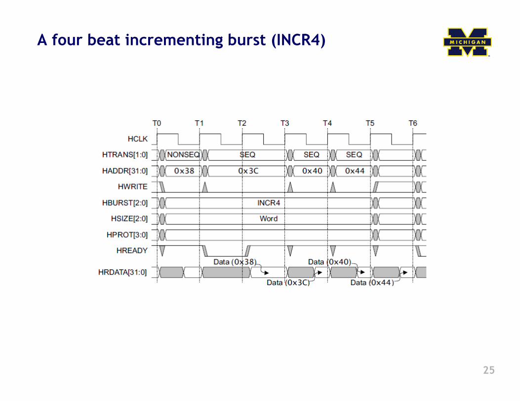
A four beat incrementing burst (INCR4)

26
An eight beat wrapping burst (WRAP8)

27
An eight beat incrementing burst (INCR8) using half-word transfers

28
An undefined length incrementing burst (INCR)

29
Multi-master AHB-Lite requires a multi-layer interconnect
• AHB-Lite is single-master
• Multi-master operation – Must isolate masters – Each master assigned to layer – Interconnect arbitrates slave
accesses
• Full crossbar switch often unneeded – Slaves 1, 2, 3 are shared – Slaves 4, 5 are local to Master 1
AHB-Lite takeaways
• AHB-Lite is a pipelined bus – Address of one transaction at the same time as data of
another transaction
• AHB-Lite deals with real-world problems – Critical-word first (for caches) – Longer data phases (burst) to reduce overhead. – Locks
• Still has flow control
30

SoyouwanttomakeaPrintedCircuitBoard…
• AttheendofthedayaPCBisjustasetofwiresthatconnectcomponents.– Buttherearesomeissues
• Thewireshaverestricteddimensionality
• Thewiresareverythin– Sohighresistance(as
conductorsgo)
• Theboardneedstoincludeholes(orpads)forthedevices.
• Youcan’teasilychangethingsonceyoubuildit.
hEp://www.linkwitzlab.com/Pluto/supplies-subw.htm,hEp://www.musicfromouterspace.com/analogsynth/SINGLEBUSSKEYBOARD2007/SINGLEBUSSKEYBOARD2007.php
PCBs–basicterminology

BasicTerminology• Thewiresyouarelayingout
arecalled“traces”or“tracks”• Insideofagiven“layer”
traceswhichcrossareelectricallyconnected.– Ifyouhavetracesonbothsides
oftheboard,youaresaidtohavetwolayers.
• Through-hole:HavingholesinthePCBdesignedtohavepinsputthroughthehole– Contrastwithsurfacemount
wheredevicegoesontop.
PCBs–basicterminology

33
PartsofaPCB
Drill holes Via Bottom side
Silkscreen (white)
Copper (pads & traces)
Soldermask (green)
PCBs–basicterminology

Vias
• Some]mesyouneedtoconnecttwotracesontwodifferentlayers.– Todothisweuseavia.– Itisjustaaplatedthroughhole• Generallysmallerthanathroughholeforapart.
PCBs–basicterminology
Clearances
• Therewillbespacebetweenthetraces,platedholesandeachother.– Youneedtomeettherequirementofthemanufacturer.
PCBs–basicterminology

Thelayeredconstruc]onofaPCB:Asixlayerboard
36
PCBs–basicterminology
Figurefromal]um.com

So,howdoIdesignaPCB?
1. Createschema]c
2. Placeparts
3. Routeinterconnect
4. Generatefiles
PCBs–designsteps

Step1:Createschema]c
• Thefirstthingyouwantissomethingthatlookslikeatextbookcircuitdiagram.Itjustshowsthedevicesandhowtheyareconnected.– Some]mesyouwillworryaboutpinoutshere(saywhenworkingwithamicroprocessormaybe)
– Butusuallyyoudon’t• Nono%onoflayoutbelongshere!
PCBs–designsteps:schema]c

Exampleschema]cPCBs–designsteps:schema]c
Whyaschema]c?
• Ingeneralitisdrawntobereadable.– Thisisprobablywhatyoursketchonpaperwouldlooklike.
– YoucanfindandfixbugsmoreeasilyherethanthePCBlayout.
PCBs–designsteps:schema]c

Step2:Placeparts
• YouneedtoplacethepaEernsontheboard.– Youneedtonotoverlapthemtothatthecomponentscanactuallyfitontheboard.
– Youwanttoleaveroomforthetracestoconnecteverything.
• Thisisverymuchanartform.– Infactyouwillfindpeoplewhorantabout“sloppy”or“unprofessional”placements.
• Sometoolswilldothisforyou.Nooneseemstolikethem.
PCBs–designsteps:placement

PaEerns• Onceyouknowwhatitis
youwanttobuild,youneedtofigureouthowtolayitoutontheboard. – Youneedtoknowhowbig
eachpieceis,andwheretheholesneedtobeplaced.
• EachdevicehasapaEernwhichshowsexactlythat.– Youwilloccasionallyneedto
createapaEern.
PCBs–designsteps:placement

Step3:Routeinterconnect
• Arouteisaconnec]onbetweendevices.– Itmayconsistofmul]pletraces
• Therearedesignruleswhichinclude:– Minimumtracewidth– Minimumspacingbetweentracesandholes– Minimumspacingbetweenholesandholes.
• Theseruleswillvarybymanufacturer.– EvenbeEer,unitswillvarybymanufacturer!– Timeforabriefaside…
PCBs–designsteps:rou]ng

Issuesofmeasure
• PCBlandusessomeinteres]ngterminology.– A“thou”isathousandthofaninch.– A“mm”isamillimeter– A“mil”isathousandthofaninch.• Thouisgenerallypreferredovermilltoavoidconfusion,butmosttools/vendorsusemill.
PCBs–anaside

Tracewidth• IngeneralmostPCBmanufacturesseemtohavetrace-widthminimumsof6-10thous.– Mostarewillingtogosmallerforaprice.
• Aruleofthumbistousea50thouminimumforpower/groundand25foreverythingelse.– Thisistodroptheresistanceofthetraces.– Ingeneralyouareworriedaboutheatdissipa]on
• Therearelotsofguidelinesforwidth/powerbutingeneralyouarelookingat:– A10cmtraceneedstobe10thouwideifitwillcarry1amp.
– 5ampsat10cmwouldrequire110thou.
PCBs–anaside

Tracewidthcon]nued
• Theproblemwithwidetracesisthattheyarehardtoroute.– Inpar]cularyoumightwishtogobetweenpinsofadevice.
• Onesolu]onistobewidenormallyand“neckdown”whenyouhaveto.– Thisismorereasonablethanyouthink.• Thinkresistorsinseries.
PCBs–anaside

Rat’snest.
• Arat’snestshowstheplacementofthedevicesandtheconnec]onsbutnottherou]ng– Automa]callygeneratedforyou.• Some]mesbeforeplacement,some]mesaler– Variesbytool.
PCBs–designsteps:rou]ng

Rou]ngforreal• Youcanusean
autoroutertorouteyourtraces– Somepeoplehatetheseasthedesignwillbe“ugly”
– Savesalotof]me.– Oddly,notasgoodasapersoncando.• Butmuchfaster.
• S]llgenerallyneedtodosome(orall)oftherou]ngbyhand– Verytedious...
PCBs–designsteps:rou]ng
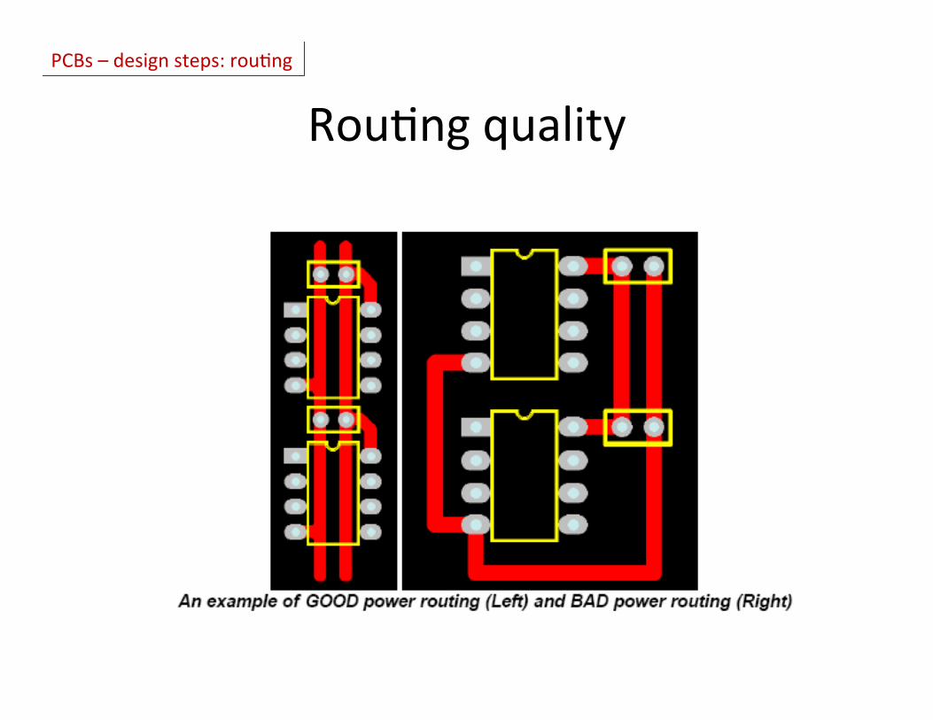
Rou]ngqualityPCBs–designsteps:rou]ng

Step4:Generatefiles• Oncethedesignisdone,asetoffilesaregenerated.
– Eachfiledescribessomethingdifferent(e.g.)• Copperonagivenlayer• Silkscreen• Soldermask
– Mostfilesarein“Gerber”format• Human-readable(barely)ASCIIformat• Hascommandslikedrawandfill.
– DrillfilesareadifferentformatcalledExcellon• Alsohuman-readable(barely)ASCIIwithloca]onsanddiametersfortheholes.
• GenerallyyouzipallthesefilesupandshipthemasasinglefiletothePCBmanufacturer.– Olenagoodideatoincludethedesignfile(s)too.
PCBs–designsteps:generatefiles
51
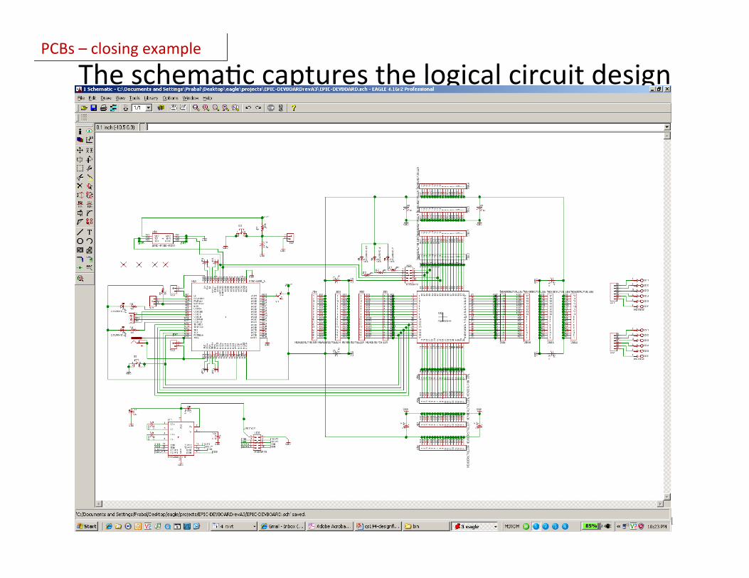
Theschema]ccapturesthelogicalcircuitdesignPCBs–closingexample

52
Floorplanningcapturesthedesiredpartloca]onsPCBs–closingexample

53
Theauto-routerplacestracksontheboard,saving]mePCBs–closingexample
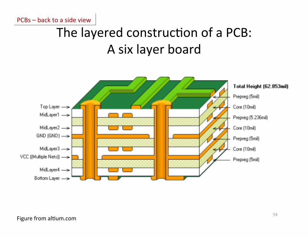
Thelayeredconstruc]onofaPCB:Asixlayerboard
54
PCBs–backtoasideview
Figurefromal]um.com