Embed Size (px)
Citation preview

INTERNATIONAL JOURNAL ON SMART SENSING AND INTELLIGENT SYSTEMS SPECIAL ISSUE, SEPTEMBER 2017
344
DESIGN OF LOW LEAKAGE CURRENT AVERAGE POWER
CMOS CURRENT COMPARATOR USING SVL TECHNIQUE
WITH PSEUDO NMOS AND TRANSMISSION GATE LOGICS
1T.R.Dinesh Kumar ,
2K.Mohana Sundaram
1 M.Anto Bennet
1*
3M.Pooja ,
3 A.P. Kokila
3K.Anusuya
1Faculty of Electronics and Communication Engineering,Vel Tech,Chennai,Tamilnadu,India
2Faculty of Electrical and Electronics Engineering,Vel Tech Multitech Dr. Rangarajan Dr.
Sakunthala Engineering College,,Chennai,Tamilnadu,India
3UG Student of Electronics and Communication Engineering,Vel Tech,Chennai,Tamilnadu,India
* Email: [email protected]
Submitted: May 27, 2017 Accepted: June 15, 2017 Published: Sep 1, 2017
Abstract- Comparatorare most widely used second electronic components after operational amplifier.
For ADC circuit we have to use the high speed and low power consumption based comparator. SVL
circuit is used tom reduce the offset voltage which requires high voltage gain. A SVL circuit can supply
maximum DC voltage to an active load circuit on request or can decrease the DC voltage supplied to a
load circuit in the standby mode was developed. SVL circuit is used with comparator which reduce the
power consumption from 258.6µw to 156.7µw. Pseudo nmos logic and transmission gate logic is used
with the SVL based current comparator which further reduce the power consumption in the standby
mode. This technique based comparator is fabricated on the tanner tool of 45nm technology.SVL
technique is mostly recommended for CMOS logic.
Index terms: current comparator, SVL circuit, pseudo nmos, transmission gate, low power consumption,
standby mode.

T.R.Dinesh Kumar, K.Mohana Sundaram, M.Pooja, A.P. Kokila and K.Anusuya
Design of low leakage current average power cmos current comparator using svl technique with pseudo
nmos and transmission gate logics
345
I. INTRODUCTION
Comparators are one of the most important elements for analog circuit design because of low
power consumption, minimum size transistors, high speed, small chip area and there are large
number of applications such as scientific computation, test circuit application and general
purpose processor component. Comparator is very attractive for memory, sensing elements,
analog to digital convertors and data receivers. The basic block diagram of comparator is
shown in fig.1.1 and fig.1.2.
II. LITERATURE SURVEY:
There are two well-known existing techniques for reducing stand-by-power(Pst).One
is multi threshold voltage cmos(MTCMOS)[10] which reduces Pst by disconnecting the power
supply through the P-MOSFET switches(SWs) with higher threshold voltage(Vth).However it
has serious drawback that it requires additional fabrication process for higher Vth and storage
circuit based on this technique cannot retain data. The another technique is variable threshold
voltage cmos(VTMOS) [11] this also faces some problem such as very slow substrate bias
controlling operation,large area and power penalty.
To solve this drawbacks, a SVL circuit which decreases the stand by power with
high speed performance have been developed. When the loads circuit is in active mode the SVL
circuit supplies maximum DC voltages through switches that are turned on i.e., “on SWs” so that
it can operate quickly.When the load circuit is in stand by mode it supplies slightly lower Vd and
higher Vs through “on SWs” so that Vdsn decreases and Vsub increases. Thus, Vth increases and
subthreshold current decreases so that Pst is reduced.
In this paper we have designed the current comparator using SVL technique with
pseudo nmos and transmission gate logic style. Thus the result compraising of power
INTERNATIONAL JOURNAL ON SMART SENSING AND INTELLIGENT SYSTEMS SPECIAL ISSUE, SEPTEMBER 2017
346
consumption of basic current comparator and SVL based current comparator with these two
logics.
III. PROPOSED SYSTEM:
SVL technique which reduces the stand by power with high speed performance was proposed in
cmos current comparator with pseudo nmos and transmission gate logic .There are three types of
SVL technique type 1 – upper svl, type 2 - lower svl, type 3 – svl circuit (combination of upper
and lower svl circuit).
In SVL circuit when control signal (CL) is applied n – sw turns on and p – sw turns off .Vdd is
applied to the inverter through n – SWs. Thus, a drain to source voltage (Vdsn) i.e., drain voltage
(Vd) of the “off n-mos” can be expressed as
Vdsn= Vdd-mv - (1)
Where v is the voltage drop of the single n-sw and m is the number of the n-sw used. Vdsn can be
changed by varying m or v. Vdsn can be decreased by increasing mv which increases the barrier
height of the “off n-mos” which further increase the Vth and reduces the leakage current. The
type 1 upper SVL circuit is shown in the figure 3.1.
In the lower SVL circuit when negative control signal is applied it turns on p-sw and n-sw is
turned off. Vss is supplied through p-SWs. The increase in the gate bias increases the Vth which
reduces the threshold current and leakage current. The type 2 lower SVL circuit is shown in the
figure 3.2.

T.R.Dinesh Kumar, K.Mohana Sundaram, M.Pooja, A.P. Kokila and K.Anusuya
Design of low leakage current average power cmos current comparator using svl technique with pseudo
nmos and transmission gate logics
347
The working of the type 3-SVL circuit is same as the combination of the upper svl circuit and
lower svl circuit and the power consumption is reduced more in this circuit. The type 3 SVL
circuit is shown in the figure3.3.
IV. CMOS CURRENT COMPARATOR CIRCUIT DESCRIPTION AND OPERATION:
The most signal processing applications of comparator is the detection of multiple threshold so
we discuss about multiple comparator circuit configuration for example a trio of simple current
comparator with outputs A,B and C are shown in figure 4.1.
We will discuss the operation of comparator A where the input current Iin is applied to the drain
of the transistor T1 and diode connnected. Transistor T2 reproduces this input current that is also
INTERNATIONAL JOURNAL ON SMART SENSING AND INTELLIGENT SYSTEMS SPECIAL ISSUE, SEPTEMBER 2017
348
reproduced by T3 to establish the threshold current Ith. If the input current is less than the
threshold current we want voltage Vds to be low. But we need the output voltage to fall low
when the threshold current exceeds the input current for that reason transistor T1 and T2 will be
operating in the saturation and linear regions.
The N-channel transistor T generates Vgs and for T1 in the saturation region
Iin = X1(W/L)1 (Vgs-VTH)2 - (2)
And for transistor T2 in the linear region
Id2=X2(W/L)2(2(Vgs-Vt2)Vds2-V2
ds2) – (3)
The identical Nmos transistor with identical(W/L) ratio has identical X‟s and Vth.To turn off the
gate Vds must be low and set the maximum allowable low logic level of the output to be about
one-third the NmosVth.let assume that the low value of the output voltage occurs when the input
current is 1.1 times as large as the threshold cuurent. when the output becomes low by using the
above two drain current equation we can solve Vgs as 1.5v.By having Vgs and input current we
can solve width to length ratio of transistor T1 and T2.
V. CMOS CURRENT COMPARATOR LOGIC STYLES :
1.PSEUDO NMOS LOGIC
2.TRANSMISSION GATE LOGIC
5.1. PSEUDO NMOS LOGIC:
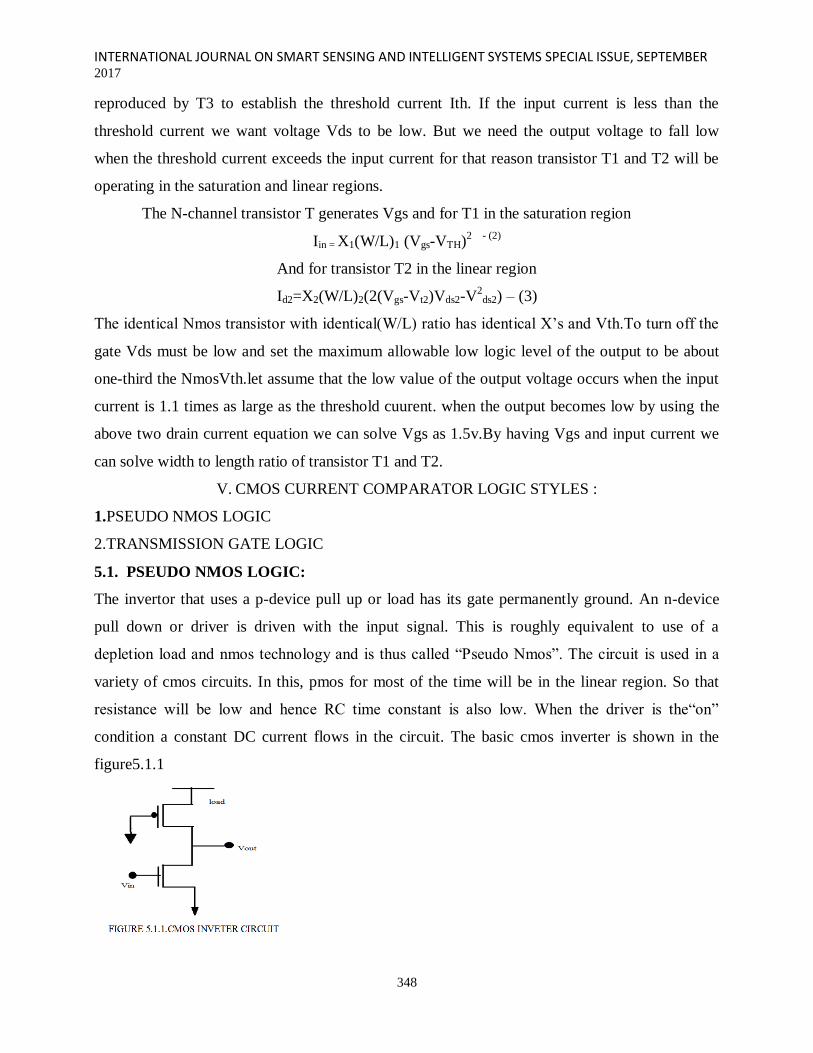
The invertor that uses a p-device pull up or load has its gate permanently ground. An n-device
pull down or driver is driven with the input signal. This is roughly equivalent to use of a
depletion load and nmos technology and is thus called “Pseudo Nmos”. The circuit is used in a
variety of cmos circuits. In this, pmos for most of the time will be in the linear region. So that
resistance will be low and hence RC time constant is also low. When the driver is the“on”
condition a constant DC current flows in the circuit. The basic cmos inverter is shown in the
figure5.1.1

T.R.Dinesh Kumar, K.Mohana Sundaram, M.Pooja, A.P. Kokila and K.Anusuya
Design of low leakage current average power cmos current comparator using svl technique with pseudo
nmos and transmission gate logics
349
5.1.1 OPERATION:
In pseudo nmos the cmos pull up network is replaced by single pmos transistor with its gate
grounded. Since the pmos is not driven by signals, it is always „on‟. The effective gate voltage
seen by the pmos transistor is Vdd. Thus overall voltage on the p channel gate is always Vdd-
Vtp. When the nmos is turned „on‟ a direct path between supply and ground exist and static
power will be drawn. However the dynamic power is reduced due to lower capacitance loading.
The logic network representation of pseudonmos logic is shown in figure 5.1.2.
The advantages of pseudo nmos is it requires less number of transistor than cmos and
transmission gate style because of this advantage speed is more. This logic is also called as
ratioed logic where its reduces dynamic power by reducing capacitive loading. It produces low
noise margin due to high VOL. It produces non-zero static power dissipation and do not provide
full output voltage swing because of pmos always „on‟. If the output is zero it has static power
dissipation and if the output is non-zero it has no static power dissipation. The schematic
representation of comparator using pseudo nmoslogic style is shown in figure 5.1.3 .
5.2. TRANSMISSION GATE:
A transmission gate or analog switch is defined as an electronic element that will selectively
block or pass a signal from the input to the output and this switch is comprised of a pmos
transistor and nmos transistor. The control gates are biased in a complementary manner so that

INTERNATIONAL JOURNAL ON SMART SENSING AND INTELLIGENT SYSTEMS SPECIAL ISSUE, SEPTEMBER 2017
350
both transistor are „on‟ or „off‟. The transmission gate is also known as bidirectional switch. The
common circuit symbol of the transmission gate is shown in figure 5.2.1.
5.2.1 OPERATION:
The values of p-gate and n-gate are expected to be opposite to each other. When the voltage on
node A i.e., n-gate is a logic 1 the complementary logic 0 is applied to node active low A i.e., p-
gate, allowing both the transistor to conduct and pass the signal at IN and OUT. When the
voltage on node active low A is a logic 0,the complementary logic 1 is applied to the node A
turning both the transistor off an forcing a high-impedance condition on both the IN and OUT
nodes. This high-impedance condition represents the third state that the channel may reflect
down stream. In all other cases drain receives an error output in which source and drain is
floating. This behaviour is summarized by the following table shown below.
p-gate n-gate Drain
0 0 M*
0 1 SOURCE
1 0 N
1 1 M*
M/N ANY M*
ANY M/N M*
*If source is N,drain is N;otherwise drain is M.
The basic circuit of transmission gate is shown in the figure 5.2.2 and the schematic
representation of the comparator using transmission gate logic style is shown in the figure 5.2.3.

T.R.Dinesh Kumar, K.Mohana Sundaram, M.Pooja, A.P. Kokila and K.Anusuya
Design of low leakage current average power cmos current comparator using svl technique with pseudo
nmos and transmission gate logics
351
VI. SIMULATION RESULT:
In this section the simulation of current comparator and the SVL modified CMOS current
comparator was designed as shown in the figure 6.1 and 6.2 and 6.3. The simulation and design
are obtained in the tanner tool using s-edit. The analysis of power consumption and delay are
obtained using t-spice simulator. The power consumption of conventional CMOS current
comparator is 258.6µw and the power consumption of SVL modified CMOS is 156.7µw where
60% of power consumption is reduced. The result shows thst SVL modified CMOS consumes
less power when compared to conventional CMOS current comparator.

INTERNATIONAL JOURNAL ON SMART SENSING AND INTELLIGENT SYSTEMS SPECIAL ISSUE, SEPTEMBER 2017
352
The simulation of CMOS current comparator with pseudo nmos logic using SVL technique is
shown in the figure 6.4 and 6.5 and 6.6. The power consumption of CMOS current comparator
with pseudo nmos is 248.75µw and for CMOS current comparator with pseudo nmos using SVL
technique is198.50µw where 80% of power consumption is reduced. The result shows that SVL
modified CMOS current comparator consumes less power.

T.R.Dinesh Kumar, K.Mohana Sundaram, M.Pooja, A.P. Kokila and K.Anusuya
Design of low leakage current average power cmos current comparator using svl technique with pseudo
nmos and transmission gate logics
353
The simulation of CMOS current comparator with transmission gate logic style using
SVL technique is shown in the figure 6.7 and 6.8 and 6.9. The power consumption of CMOS
current comparator with transmission gate logic is 435.9µw and for CMOS current comparator
with transmission gate logic using SVL technique is 289.7µw where 55% of power consumption
is reduced. The result shows that SVL modified CMOS current comparator consumes less power.

INTERNATIONAL JOURNAL ON SMART SENSING AND INTELLIGENT SYSTEMS SPECIAL ISSUE, SEPTEMBER 2017
354
VII. CONCLUSION:
A SVL self controllable voltage level circuit with current comparator which overcomes
the drawbacks of MTCMOS and VTCMOS was developed. This SVL circuit can dynamically
reduce Vdsn drain to source voltage and increase the substrate bias of MOSFET which is in off
condition in the stand by load circuit. After simulations of designs with pseudo nmos and
transmission gate logic final results are obtained for power consumption. The result shows that
Pseudo nmos logic consumes low power when compared to transmission gate logic style.

T.R.Dinesh Kumar, K.Mohana Sundaram, M.Pooja, A.P. Kokila and K.Anusuya
Design of low leakage current average power cmos current comparator using svl technique with pseudo
nmos and transmission gate logics
355
An important factor is that output voltage swing is better in cmos design and transmission gate
logic style. But transmission gate requires more number of transistors when compared to cmos
design style. The drawback in transmission gate can be overcome in pseudo nmos logic which
requires less number of transistor. The power consumption of the current comparator with pseudo
nmos and transmission gate logic using SVL circuit consumes less power when compared to
normal current comparator with these logics.
REFERENCES
[1] Aizat Azmi, Ahmad Amsyar Azman, Sallehuddin Ibrahim, and Mohd Amri Md Yunus,
“Techniques In Advancing The Capabilities Of Various Nitrate Detection Methods: A Review”,
International Journal on Smart Sensing and Intelligent Systems., VOL. 10, NO. 2, June 2017, pp.
223-261.
[2] Tsugunosuke Sakai, Haruya Tamaki, Yosuke Ota, Ryohei Egusa, Shigenori Inagaki, Fusako
Kusunoki, Masanori Sugimoto, Hiroshi Mizoguchi, “Eda-Based Estimation Of Visual Attention
By Observation Of Eye Blink Frequency”, International Journal on Smart Sensing and Intelligent
Systems., VOL. 10, NO. 2, June 2017, pp. 296-307.
[3] Ismail Ben Abdallah, Yassine Bouteraa, and Chokri Rekik , “Design And Development Of 3d
Printed Myoelctric Robotic Exoskeleton For Hand Rehabilitation”, International Journal on
Smart Sensing and Intelligent Systems., VOL. 10, NO. 2, June 2017, pp. 341-366.
[4] S. H. Teay, C. Batunlu and A. Albarbar, “Smart Sensing System For Enhanceing The
Reliability Of Power Electronic Devices Used In Wind Turbines”, International Journal on Smart
Sensing and Intelligent Systems., VOL. 10, NO. 2, June 2017, pp. 407- 424
[5] SCihan Gercek, Djilali Kourtiche, Mustapha Nadi, Isabelle Magne, Pierre Schmitt, Martine
Souques and Patrice Roth, “An In Vitro Cost-Effective Test Bench For Active Cardiac Implants,
Reproducing Human Exposure To Electric Fields 50/60 Hz”, International Journal on Smart
Sensing and Intelligent Systems., VOL. 10, NO. 1, March 2017, pp. 1- 17
[6] P. Visconti, P. Primiceri, R. de Fazio and A. Lay Ekuakille, “A Solar-Powered White Led-
Based Uv-Vis Spectrophotometric System Managed By Pc For Air Pollution Detection In

INTERNATIONAL JOURNAL ON SMART SENSING AND INTELLIGENT SYSTEMS SPECIAL ISSUE, SEPTEMBER 2017
356
Faraway And Unfriendly Locations”, International Journal on Smart Sensing and Intelligent
Systems., VOL. 10, NO. 1, March 2017, pp. 18- 49
[7] Samarendra Nath Sur, Rabindranath Bera and Bansibadan Maji, “Feedback Equalizer For
Vehicular Channel”, International Journal on Smart Sensing and Intelligent Systems., VOL. 10,
NO. 1, March 2017, pp. 50- 68
[8] Yen-Hong A. Chen, Kai-Jan Lin and Yu-Chu M. Li, “Assessment To Effectiveness Of The
New Early Streamer Emission Lightning Protection System”, International Journal on Smart
Sensing and Intelligent Systems., VOL. 10, NO. 1, March 2017, pp. 108- 123
[9] Iman Heidarpour Shahrezaei, Morteza Kazerooni and Mohsen Fallah, “A Total Quality
Assessment Solution For Synthetic Aperture Radar Nlfm Waveform Generation And Evaluation
In A Complex Random Media”, International Journal on Smart Sensing and Intelligent Systems.,
VOL. 10, NO. 1, March 2017, pp. 174- 198
[10] P. Visconti ,R.Ferri, M.Pucciarelli and E.Venere, “Development And Characterization Of A
Solar-Based Energy Harvesting And Power Management System For A Wsn Node Applied To
Optimized Goods Transport And Storage”, International Journal on Smart Sensing and Intelligent
Systems., VOL. 9, NO. 4, December 2016 , pp. 1637- 1667
[11] YoumeiSong,Jianbo Li, Chenglong Li, Fushu Wang, “Social Popularity Based Routing In
Delay Tolerant Networks”, International Journal on Smart Sensing and Intelligent Systems.,
VOL. 9, NO. 4, December 2016 , pp. 1687- 1709
[12] Seifeddine Ben Warrad and OlfaBoubaker, “Full Order Unknown Inputs Observer For
Multiple Time-Delay Systems”, International Journal on Smart Sensing and Intelligent Systems.,
VOL. 9, NO. 4, December 2016 , pp. 1750- 1775
[13] Rajesh, M., and J. M. Gnanasekar. "Path observation-based physical routing protocol for
wireless ad hoc networks." International Journal of Wireless and Mobile Computing 11.3 (2016):
244-257.
[14]. Rajesh, M., and J. M. Gnanasekar. "Congestion control in heterogeneous wireless ad hoc
network using FRCC." Australian Journal of Basic and Applied Sciences 9.7 (2015): 698-702.
[15]. Rajesh, M., and J. M. Gnanasekar. "GCCover Heterogeneous Wireless Ad hoc Networks."
Journal of Chemical and Pharmaceutical Sciences (2015): 195-200.

T.R.Dinesh Kumar, K.Mohana Sundaram, M.Pooja, A.P. Kokila and K.Anusuya
Design of low leakage current average power cmos current comparator using svl technique with pseudo
nmos and transmission gate logics
357
[16]. Rajesh, M., and J. M. Gnanasekar. "CONGESTION CONTROL USING AODV
PROTOCOL SCHEME FOR WIRELESS AD-HOC NETWORK." Advances in Computer
Science and Engineering 16.1/2 (2016): 19.
[17]. Rajesh, M., and J. M. Gnanasekar. "An optimized congestion control and error management
system for OCCEM." International Journal of Advanced Research in IT and Engineering 4.4
(2015): 1-10.
[18]. Rajesh, M., and J. M. Gnanasekar. "Constructing Well-Organized Wireless Sensor
Networks with Low-Level Identification." World Engineering & Applied Sciences Journal 7.1
(2016).
[19] L. Jamal, M. Shamsujjoha, and H. M. Hasan Babu, “Design of optimal reversible carry look-
ahead adder with optimal garbage and quantum cost,” International Journal of Engineering and
Technology, vol. 2, pp. 44–50, 2012.
[20] S. N. Mahammad and K. Veezhinathan, “Constructing online testable circuits using
reversible logic,” IEEE Transactions on Instrumentation and Measurement, vol. 59, pp. 101–109,
2010.
[21] W. N. N. Hung, X. Song, G. Yang, J. Yang, and M. A. Perkowski, “Optimal synthesis of
multiple output boolean functions using a set of quantum gates by symbolic reachability
analysis,” IEEE Trans. on CAD of Integrated Circuits and Systems, vol. 25, no. 9, pp. 1652–
1663, 2006.
[22] F. Sharmin, M. M. A. Polash, M. Shamsujjoha, L. Jamal, and H. M. Hasan Babu, “Design of
a compact reversible random access memory,” in 4th IEEE International Conference on
Computer Science and Information Technology, vol. 10, june 2011, pp. 103–107.
[23] Dr. AntoBennet, M, Sankar Babu G, Suresh R, Mohammed Sulaiman S, Sheriff M,
Janakiraman G ,Natarajan S, “Design & Testing of Tcam Faults Using TH Algorithm”, Middle-
East Journal of Scientific Research 23(08): 1921-1929, August 2015 .
[24] Dr. AntoBennet, M “Power Optimization Techniques for sequential elements using pulse
triggered flipflops”, International Journal of Computer & Modern Technology , Issue 01
,Volume01 ,pp 29-40, June 2015.