Embed Size (px)
Citation preview

Design of CPU Simulation Software for ARMv7 Instruction Set Architecture
Author: Dillon Tellier
Advisor: Dr. Christopher Lupo
Date: June 2014
1 INTRODUCTION
Simulations have long been a part of the engineering process in both the professional and academic domain. From a
pedagogic standpoint, simulations allow students to explore the dynamics of engineering scenarios by controlling
variables, taking measurements, and observing behavior which would be difficult or impossible without simulation. One
such tool is a CPU simulator used in Cal Poly’s Computer Architecture classes; this software simulates an instruction
accurate operation of a computer processor and reports statistics regarding the execution of the supplied compiled
machine code. For the last several years Cal Poly’s computer architecture classes have used a previous version of the
CPU simulator that simulated the MIPS architecture. Although the previous system was a functional and useful tool, it
had significant room for improvement. Although it was once common, the MIPS architecture is much relevant in
industry today, especially in the face of its current competitors. From a technical standpoint the MIPS architecture is
very similar to other common RISC architectures, but as current technology evolves the usefulness of a MIPS simulator in
helping students understand the operation of modern CPUs will continue to diminish. Another place for improvement
was in the design of the simulator itself. Since class assignments involving the CPU simulator often require the students
to modify an intentionally incomplete version of the simulator, students must also understand the design of the
simulator software itself. Though it is functional, the design of the MIPS simulator was minimally documented and the
logical organization of the code obfuscates the system being simulated. This has been a source of frustration for not only
students, but also for the professors who teach the courses in which the simulator is used. I sought to address these
problems in 2 fundamental ways: first, by migrating the simulation to the ARMv7-A architecture and secondly, by doing
a complete structural redesign of the simulator as to make the simulation architecture as transparent as possible vis-à-
vis the architecture being simulated.
2 BACKGROUND
2.1 INSTRUCTION SET ARCHITECTURES The design of a central processing unit (CPU) can be, in its simplest form, described as a two-parts. The instructions set
architecture (ISA), which describes the operations than can be performed by the CPU and the exact behavior of the
those operations, and the microarchitecture, which is the way that the ISA is implement using semiconductor devices in
the physical device itself. These two parts can be designed by the same firm, but often these two parts are designed
separately with one firm designing the ISA and subsequently licensing the ISA to manufacturers who then develop
methods of converting the architectures to a microchip.
ISA’s can be classified into two families, Reduced Instruction Set Computing (RISC) and Complex Instruction Set
Computing (CISC). RISC devices, unlike CISC devices, only perform one basic operation per instruction. Although this may
initially seem like a disadvantage, RISC architectures are easier to develop and debug due to the fact that every internal
operation can be mapped to a single instruction. Both the MIPS (Microprocessor Without Interlocked Pipeline Stages)
and ARM (Advanced RISC Machines) architectures follow the RISC design model which makes them ideal for educational
environments, especially simulations.
2.2 INSTRUCTION CYCLES
2.2.1 Overview
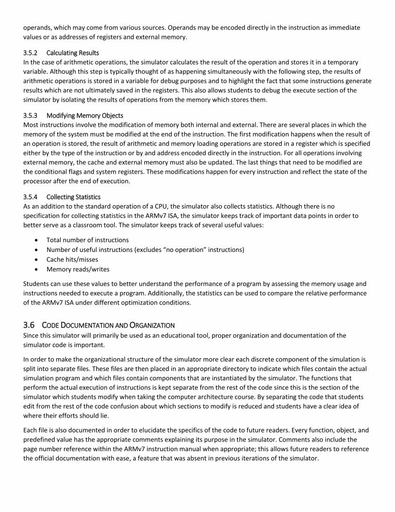
For any ISA the instruction cycle describes the abstract workflow and dataflow of the processor during the execution of a
single instruction. For RISC devices in general follow the same basic architecture: first an instruction is fetched from the
instruction memory at the location pointed to by a program counter, secondly the instruction is decoded and the
operation to be performed is identified, and lastly the instruction is executed and the effects of the operation are
reflected in the state of the system. Instruction set architectures describe the types of instructions that can exist, how
the instructions are decoded, and what the internal and external state of the system should be after the execution of an
instruction.
2.2.2 Fetch
The first part of the instruction cycle is the fetch operation. A
single instruction is a binary number of fixed width stored in the
instruction segment of random access memory (RAM). A
counter, called the Program Counter (PC) keeps track of the
current instruction of the program. After the end of each
instruction the PC is incremented thus pointing to a new
instruction; some instructions however may modify the value of
the PC so that it points to a different segment of memory, this
allows for jumps between sections of the program.
2.2.3 Decode
The next step of the cycle is the decoding of the instruction. For
any given instruction, the type of operation and the operands are
stored within the instruction itself. At least one segment of any
instruction represents the type of operation that needs to be
performed, these segments are known as opcodes. Different
opcodes usually represent different instructions although some instructions are mapped to by multiple opcodes. The
remaining bits in the instruction can represent different things depending on the type of instruction, often these bits
represent the operands of arithmetic manipulations which are typically registers, immediate values, or some
combination of both. For instructions that do not require all the bits to express the operation and operands then the
remaining bits are usually fixed to a certain value to ensure that instructions always have the same length.
2.2.4 Execute
The last part of the cycle is the execution of the operation. Once the instruction type and operands are known then the
CPU can perform the requested operation. The execution step is often thought of being divided into 3 steps itself. First
any arithmetic result is calculate, secondly the result is written to the appropriate destination register in internal
memory, and lastly any operations involving the loading or storing of instructions in external memory will be completed.
At the end of the execute cycle the state of the CPU and external memory reflect the end of the operation.
2.3 MEMORY
2.3.1 Registers
The most fundamental memory structure for a CPU is the register, a form of very rapid memory that is integrated within
the microarchitecture of the CPU. Because of the difficulty and expense in creating registers modern CPUs only contain a
Image 1: Instruction Cycle

handful of registers, typically 16 – 64 registers in modern CPUs. Each register holds a predetermined amount of data,
usually the same number of bits as an instruction or memory address. Registers hold the most immediately necessary
information for the processor to operate such as the program counter, the stack pointer, the operands of the current
function, and the return value of the previous function.
2.3.2 External Memory
Since a CPU can only perform operations on the limited data in its registers it must store any additional necessary data in
external memory. The values within registers can be stored in main memory which consists of Random Access Memory
(RAM) and any long term non-volatile storage like a hard drive or SSD. The contents of main memory can also be loaded
into a register when the CPU needs to use that data. Although external memory can be much larger than the registers it
is also much slower.
2.3.3 Caches
Caches are memory structures that act as an intermediary between internal memory (registers) and external memory.
Caches are also internal to a CPU and tend to fall between registers and RAM in capacity. Caches are slower than
registers but are still much faster than external memory. When a value is requested from main memory a CPU will first
check its cache for the value; if the cache entry is valid (cache hit) then the time to go to external memory was saved, if
the entry is not found (cache miss) then the data request either moves to a bigger but slower cache, or if none exists, to
external memory. A fixed algorithm determines how the cache is populated and how cache contents are replaced in
order to maximize the ratio of hits.
2.3.4 CPU Condition Flags
Condition flags are 1-bit registers used by the CPU to rapidly check whether or not an instruction met a certain common
condition. In most CPUs the condition flags represent things like whether the previous instruction’s result was zero,
negative, or caused integer overflow. These flags are critical in maintaining the efficient operation of a CPU since
dedicated instructions for checking certain conditions are not needed beyond verifying the value of a register.
3 DESIGN
3.1 SYSTEM OVERVIEW
3.2 PRELIMINARY DESIGN DECISIONS
3.2.1 Why ARMv7-A?
One of the principal differences between the previous simulation and my own system is the migration from the older
MIPS architecture to the newer ARMv7-A architecture. The primary motivation for this transition is the exponential
increase in the relevance of ARM processors in the market, especially in the mobile, embedded, and low power
segments. Using a more modern architecture will expose students to more current technologies which they may
encounter in their careers.
The ARM ISA has been revised several times since its inception. The newest revision is eight version (v8) but the seventh
version (v7) was selected since v8 is new enough that most firms are still designing the build environments and
microarchitectures for it. Although there are some differences from version to version most revisions build upon each
other which means that a conversion to a newer version is significantly easier than a migration to a new ISA.
The ARM ISA also has different profiles which are subtly different versions of the ISA that are tuned for different
scenarios. The “A” (application) profile of the architecture (v7-A) is the most general version of the instruction sets and
was chosen because it is the canonical instruction set and includes all possible subsets of instructions from the other

revisions. The following sections will define the specifics of the ARMv7 ISA, the differences between MIPS, and the way
in which my system simulates the architecture.
3.2.2 Programming Language Choice
The entire codebase for the simulator is written in C++, like its predecessor, for several reasons. The main reason why
C++ was chosen was for its flexibility; by allowing for a mix of object-oriented and procedural programming styles,
sections of the simulator could be written in the style that was clearest and best suited for presenting the simulator
code in a way that was transparent to the process it is simulating. Additionally, C++ programs do not require a virtual
runtime environment to execute and take advantage of some of the object-oriented features that make the code
understandable. This makes the programs easier to run and test on the university’s servers as well as minimizing any
additional external factors which might affect the ability of the code to produce instruction accurate results.
3.2.3 Input file format
The simulator requires an objdump of the binary file as the input. The objdump is run with the –s and –x flags to ensure
that the different segments within the binary file are pre-parsed and the program counter can be determined. The
program then parses this file to load the instruction and data memory.
3.3 MEMORY MODEL
3.3.1 Registers
The ARMv7 ISA defines 16 registers which are each register
contains 32 bits. Within the simulator the registers are stored as a
Vector of register types which are redefined unsigned integers.
Certain registers have specific functions: the stack pointer, link
register, and program counter are all mapped to registers 13-15
respectively. Of the thirteen remaining registers some are defined
for specific uses by convention, i.e. the hardware does not
enforce their contents but assemblers will always use the same
location to represent things like the return value of a function
(register 0) or the arguments of the current function (registers 1-
4). The simulator code maps the specific names of the registers to
their associated register values to simplify the addressing of
registers and to clearly indicate when a register is being used for
its nominal purpose in the case of registers 0-12.
3.3.2 External Memory
Since an ISA does not dictate the architecture of external memory
but, external memory is required for the execution of virtually all
programs, an abstract representation of external memory exists
within the simulator. External memory in the simulator is divided
into data memory and instruction memory with each memory object being a Map that uses 32-bit memory address as a
keys for 32-bit data values. Accesses to the memory are made as simple as possible by ignoring the timing specifics and
direct physical continuity of data i.e. from the simulator’s point of view there is no time disparity between accessing
main memory and accessing registers. The external memory structures in the simulator still exist however to maintain
the correct instruction count and results of the CPU operations. By keeping track of statistics regarding memory accesses
within the simulator information about the runtime of the program can be determined without directly simulating the
difference in time between different memory accesses.
Image 2: ARMv7 Registers [5.1]

3.3.3 Caches
Like external memory, cache architectures are not directly included in an ISA. Unlike external memory, caches are not
necessary for simulating an ARMv7 processor since the existence of a cache is to speed up memory access and the
simulator does not directly incorporate measurements of execution time at the instruction level. A single tiered cache
however is included in order to collect more statistics about the typical operation of an ARM processor during
simulation. Like the external memory, accesses to the cache are kept as simple as possible in order to keep the scope of
simulation mainly on the behavior of the CPU according to its ISA.
3.4 INSTRUCTION PROCESSING
3.4.1 Format
The ARMv7 ISA defines the length of an instruction as a 32 bit word. The simulator contains a redefinition of a 32-bit
unsigned integer to represent the raw instruction before decoding. An instruction class also exists that represents a
decoded instruction by regrouping the raw value of the instruction with other data and operations related to the
decoding of an instruction. Each instruction object is constructed from a raw 32-bit instruction type.
3.4.2 Fetching
A raw 32-bit instruction is fetched from the instruction memory address pointed to by the program counter register. In
the simulator the instructions are retrieved from memory and are used to construct the instruction object that the rest
of the simulator uses to perform the operation.
3.4.3 Decoding
Instruction decoding in ARMv7, like MIPS, involves identifying opcodes within the raw instructions. Unlike simpler
architectures, ARM has variable opcode locations which require a tiered decoding approach. The first round of decoding
determines which instruction group the instruction belongs to. For each instruction group a different set of opcodes
within the same raw instruction may represent an individual instruction or another sub-group of instructions with its
own set of opcode locations.
The simulator mirrors this
tiered decode by separating
the methods which decode
different groups and sub-
groups. The primary decode
method calls on secondary
decode methods which in
turn may return an
instruction or call a tertiary
decode etc. Once the final
level of decoding has been
reached the appropriate
opcode variable is returned
and stored as a field within
the instruction object. Since
the ARMv7 documentation
also portrays the decode
process by groups and sub-
groups of instructions each
function can be associated
with the exact location in the
documentation that explains
the process occurring in the

specific method. The combination of separating the decode process into tiered methods and documenting each decode
stage makes the decoding process much more understandable to anyone who will read the code.
Image 3: Tiered Decoding [6.1]
One main feature of the ARMv7 ISA decoding scheme is the inclusion of a conditional preposition in most instructions.
The conditional preposition is a 4-bit wide field at the beginning of some instructions that specifies a condition that must
be met for the instruction to be successfully decoded. Each condition represents the state of the four condition flags
found in the ARMv7 ISA: the carry flag, the zero flag, the overflow flag, and the negative flag. Instructions who do not
meet this requirement are decoded to a “no operation” instruction. By checking for conditionals during decode, the
ARMv7 ISA reduces the number of instructions necessary to run any program by removing the need to dedicate an
entire instruction to checking whether a condition situations is met, a common recurring action in most programs.
Table 1: Conditional Codes [6.1]
The decode process in this simulator is limited to decoding the most common instruction groups, namely integer
arithmetic, basic memory operations, and stack management. Instructions for floating-point numbers, memory
virtualization, and parallelization return an invalid instruction type in the simulator in order to simplify the code. Since
the unsupported instructions typically require the most hardware support exterior from the CPU they are the most
difficult to properly simulate and are not necessary for many useful simulations. The design of the simulator is as such
that these instructions can be added as an extension in the future.
3.5 EXECUTING INSTRUCTIONS
3.5.1 Identifying Operands
Once an instruction has been decoded the execution portion of the cycle can begin. The first part of executing an
instruction is identifying what operands are needed for the operation. Instructions may have between zero and two
operands, which may come from various sources. Operands may be encoded directly in the instruction as immediate
values or as addresses of registers and external memory.
3.5.2 Calculating Results
In the case of arithmetic operations, the simulator calculates the result of the operation and stores it in a temporary
variable. Although this step is typically thought of as happening simultaneously with the following step, the results of
arithmetic operations is stored in a variable for debug purposes and to highlight the fact that some instructions generate
results which are not ultimately saved in the registers. This also allows students to debug the execute section of the
simulator by isolating the results of operations from the memory which stores them.
3.5.3 Modifying Memory Objects
Most instructions involve the modification of memory both internal and external. There are several places in which the
memory of the system must be modified at the end of the instruction. The first modification happens when the result of
an operation is stored, the result of arithmetic and memory loading operations are stored in a register which is specified
either by the type of the instruction or by and address encoded directly in the instruction. For all operations involving
external memory, the cache and external memory must also be updated. The last things that need to be modified are
the conditional flags and system registers. These modifications happen for every instruction and reflect the state of the
processor after the end of execution.
3.5.4 Collecting Statistics
As an addition to the standard operation of a CPU, the simulator also collects statistics. Although there is no
specification for collecting statistics in the ARMv7 ISA, the simulator keeps track of important data points in order to
better serve as a classroom tool. The simulator keeps track of several useful values:
Total number of instructions
Number of useful instructions (excludes “no operation” instructions)
Cache hits/misses
Memory reads/writes
Students can use these values to better understand the performance of a program by assessing the memory usage and
instructions needed to execute a program. Additionally, the statistics can be used to compare the relative performance
of the ARMv7 ISA under different optimization conditions.
3.6 CODE DOCUMENTATION AND ORGANIZATION Since this simulator will primarily be used as an educational tool, proper organization and documentation of the
simulator code is important.
In order to make the organizational structure of the simulator more clear each discrete component of the simulation is
split into separate files. These files are then placed in an appropriate directory to indicate which files contain the actual
simulation program and which files contain components that are instantiated by the simulator. The functions that
perform the actual execution of instructions is kept separate from the rest of the code since this is the section of the
simulator which students modify when taking the computer architecture course. By separating the code that students
edit from the rest of the code confusion about which sections to modify is reduced and students have a clear idea of
where their efforts should lie.
Each file is also documented in order to elucidate the specifics of the code to future readers. Every function, object, and
predefined value has the appropriate comments explaining its purpose in the simulator. Comments also include the
page number reference within the ARMv7 instruction manual when appropriate; this allows future readers to reference
the official documentation with ease, a feature that was absent in previous iterations of the simulator.

3.7 EXTENSIONS, MODIFICATIONS, AND FUTURE REVISION The last main goal of this simulator is to make it adaptable for extensions and modifications. In the future, students will
be able to extend the functionality of the system to even more accurately represent the operation of an ARM CPU. Some
areas in which future students will be able to expand on the simulator are: support for expanded instruction groups and
pipelining/cycle-accuracy.
The current system only supports the basic sets of instructions necessary to execute simple programs. The framework
for decoding and executing instructions however, supports decoding all instructions. Students in the future may want to
modify the code so that the entire set of instructions are allowable. These expanded instructions include floating-point
arithmetic, Single Instruction Multiple Data (SIMD) operations, and memory virtualization primitives. All of these
instruction sets will require a modification of the memory model in order to work, with many of the abstractions that
simplified the current model needing to be made more specific. With the full instruction set the simulator will be able to
work on a much wider range of programs which are more complex than the basic integer arithmetic based programs
that the current system executes.
The other area in which the simulator can be improved is in providing cycle specific results. Since the current simulator’s
goal is to provide instruction accurate results the timing specifics of a single instruction are not simulated. Additionally,
unlike real CPUs, the simulator does not pipeline its instructions, which is the process of starting one instruction cycle
while another one is still completing in a manner such that they do not overlap on the same section of the instruction
cycle. A pipelined simulator means that statistics recorded can be as accurate as possible down to the each clock cycle.
Cycle level accuracy also offers more valuable data regarding the time of execution of programs on ARM simulators.
Like any engineering system, expansions to the simulator will lead to an increase in the complexity of the system. If the
system becomes too complex it may become a less useful tool in the context of Cal Poly’s undergraduate computer
architecture classes. Future expansions of the project may be completed within the scope of a graduate level class, or as
a part of a graduate thesis.
4 CONCLUSION
Although the newest version of the CPU simulator is not
entirely functional, success was had in setting up the
framework for the simulation as well as parsing and
decoding the instructions. The system is able to
successfully compile, parse, and decode the instructions
of all the test files at all optimization levels. In the future
this design can serve as a guideline for continuing the
design and implementation of the ARM simulator in
order to achieve a complete and useful pedagogic tool.
The continuation of the project will also serve as an
experiment in the maintaining of a codebase across
multiple generations of students within the same
university; the ideal situation in the future would be a
piece of software where each version builds upon the
last with the effort of many students cumulating into a
useful tool that the CPE department at Cal Poly can use
for many years to come.
Image 4: Parsed and Decoded data

5 APPENDIX A: ADDITIONAL DIAGRAMS & CHARTS
5.1 SYSTEM DIAGRAM
6 APPENDIX B: REFERENCE DOCUMENTS
6.1 ARMV7-AR REFERENCE MANUAL (ISSUE C): http://infocenter.arm.com/help/index.jsp?topic=/com.arm.doc.ddi0406c/index.html
6.2 MIPS REFERENCE MANUAL (V5.03): http://www.imgtec.com/mips/architectures/mips32.asp