Embed Size (px)
Citation preview
7 DESIGN OF COMPUTER
INSTRUCTION SET AND THE CPU
This chapter describes the design of the instruction set and the central processor unit (CPU). Topics include op-code encoding, design of typical microprocessor registers, the arithmetic logic unit (ALU), and the control unit.
7.1
A program consists of a sequence of instructions. An instruction performs operations on stored data. There are two components in an instruction: an op-code field and an address field. The op-code field defines the type of operation to be performed on data, which may be stored in a microprocessor register or in the main memory. The address field may contain one or more addresses of data. When data are read from or stored into two or more addresses by the instruction, the address field may contain more than one address. For example, consider the following instruction:
MOVE DO, D1
Desim of the ComDuter Instructions
Op-code field Address field Assume that this computer uses DO as the source register and D 1 as the destination
register. This instruction moves the contents of the microprocessor register DO to register D 1. The number and types of instructions supported by a microprocessor vary from one microprocessor to another and primarily depend on the microprocessor architecture. The number of instructions supported by a typical microprocessor depends on the size of the op-code field. For example, an 8-bit op-code can specify a maximum of 256 unique instructions.
As mentioned before, a computer only understands 1 ’s and 0’s. This means that the computer can execute an instruction only if it is in binary. A unique binary pattern must be assigned to each op-code by a process called “op-code encoding.”
The Block code method is one of the simplest techniques of designing instructions. In this approach, a fixed length of binary pattern is assigned to each op-code. For example, an n-bit binary number can represent 2” unique op-codes. Consider for example, a hypothetical instruction set shown in Figure 7.1. In this figure, there are 8 different instructions that can be encoded using three bits i,, i,, i, as shown in Figure 7.2. A 3-to-8 decoder can be used to encode the 8 hypothetical instructions as shown in Figure 7.3.
An n-to-2” decoder is required for an n-bit op-code. As n increases, the cost of the decoder and decoding time will also increase. In some op-code encoding techniques such as
237
Fundamentals of Digital Logic andhficrocomputer Design. M. Rafiquzzaman Copyright 0 2005 John Wiley & Sons, Inc.
238 Fundamentals of Digital Logic and Microcomputer Design
the “expanding op-code” method, the length of the instruction is a function of the number of addresses used by the instruction. For example, consider a 16-bit instruction in which the lengths of the op-code and address fields are 5 bits and 1 1 bits respectively. Using such an instruction format, 32 ( F ) operations allowing access to 2048 (2”) memory locations can be specified. Now, if the size of the instruction is kept at 16 bits but the address field is increased to 12 bits, the op-code length will then be decreased to 4 bits. This change will specify 16 (24) operations with access to 4096 (212) memory locations. Thus, the number of
Instruction Operation Performed
MOVE reg,, reg,
CLR reg reg - 0
ADD reg,, reg,
SUB reg,, reg,
AND reg,, reg,
OR reg,, reg,
reg, - reg,
reg, + reg, + reg,
reg, + reg - reg,
reg, - reg, AND reg,
reg, - reg, OR reg,
I N C reg
JMP addr
reg + reg + 1
PC - addr; Unconditionally Jump to addr
FIGURE 7.1 A hypothetical instruction set
Instruction
MOVE
CLR
ADD
SUB
AND
OR
I N C
JMP
3-Bit Op-Code
4 i , ill
0 0 0
0 0 1
0 1 0
0 1 1
1 0 0
1 0 1
1 1 0
1 1 1
FIGURE 7.2 Op-code encoding using block code
FIGURE 7.3 Instruction decoder

Design of Computer Instruction Set and the CPU 239
operations is reduced by 50% and the number of memory locations is increased by 100%. This concept is used in designing instructions with expanding op-code technique.
Consider an instruction format with 8-bit instruction length and a 2-bit op-code field. Four unique two-address (3 bits for each address) instructions can be specified. This is depicted in Figure 7.4. If three rather than four two-address instructions are used, eight one-address instructions can be specified. This is shown in Figure 7.5. The length of the op-code field for each one-address instruction is 5 bits. Thus, the length of the op-code field increases as the number of address field is decreased. Now, if the total number of one-address instructions is reduced from 8 to 7, then eight 0-address instructions can also be specified. This is shown in Figure 7.6.
7.2 Reduced Instruction Set ComDuter (RISC)
RISC, which stands for reduced instruction set computer, is a generation of faster and inexpensive machines. The initial application of FUSC principles has been in desktop workstations. Note that the PowerPC is a RISC microprocessor. The basic idea behind
OP- Code Address 1 Address 2 (2-bits) (3-bits) (3-bits)
i , i,
0 0 x2 XI xo Y2 YI Yo
0 1 x2 XI xo Y2 YI Yo
1 0 x2 xi xo Y2 Yl Yo
1 1 x2 XI xo Y2 YI Yo
FIGURE 7.4 Four two-address instructions
OP code Address 1 Address 2 (3 bits) (3 bits)
i 1 io
x 2 x, xo
x 2 x, xo
Y, Y, Y o
Y, Y, Y o instructions
1 0 x z x, xo Y, Y, Yo
5-b1l+( 1 1 0 0 0 1 Y , Y , Y o opcode 0 0 1 Y, Y, Yo
1 1 0 1 0 Y , Y , Y o
1 1 1 0 0 Y , Y , Y o 1 1 1 0 1 Y , Y , Y o 1 1 1 1 0 Y , Y , Y o
1 1 1 1 1 Y , Y , Y O Y , Y , Y o
1 1 0 1 1 Y z Y , Y o Eight 1 -address
FIGURE 7.5 Three 2-address and eight 1 -address instructions

240 Fundamentals of Digital Logic and Microcomputer Design
1 1 0 1 1 Y I Y , Y 1 1 1 0 0 y, y, y 1 1 1 0 1 Y , Y , Y 1 1 1 1 0 y2 y, y
1 -address
&bit +I 1 1 1 1 1 0 0 0 I oocode 1 1 1 1 1 0 0 1 Eight 1 1
\ ' : : )-address nstructions
1 1 1 _ _ _ _ _ _
0 1 0 _ _ _ _ _ _
FIGURE 7.6 5 two-address, 7 one-address, and 8 zero-address instr tions
RISC is for machines to cost less yet run faster, by using a small set of simple instructions for their operations. Also, RISC allows a balance between hardware and software based on functions to be achieved to make a program run faster and more efficiently. The philosophy of RISC is based on six principles: reliance on optimizing compilers, few instructions and addressing modes, fixed instruction format, instructions executed in one machine cycle, only call/return instructions accessing memory, and hardwired control.
The trend has always been to build CISCs (complex instruction set computers), which use many detailed instructions. However, because of their complexity, more hardware would have to be used. The more instructions, the more hardware logic is needed to implement and support them. For example, in a RISC machine, an ADD instruction takes its data from registers. On a CISC, each operand can be stored in any of many different forms, so the compiler must check several possibilities. Thus, both RISC and CISC have advantages and disadvantages. However, the principles of understanding optimizing compilers and what actually happens when a program is executed lead to RISC.
Case Study: RISC I (University of California, Berkeley) The RISC machine presented in this section is the one investigated at the University of California, Berkeley. The RISC I is designed with the following design constraints:
1. Only one instruction is executed per cycle. 2. All instructions have the same size. 3. Only load and store instructions can access memory. 4. High-level languages (HLL) are supported. Two high level Languages (C and Pascal) were supported by RISC I. A simple
architecture implies a fewer transistors, and this leads to the fact that most pieces of a RlSC HLL system are in software. Hardware is utilized for time-consuming operations. Using C and Pascal, a comparison study was made to determine the frequency of occurrence of particular variable and statement types. Studies revealed that integer constants appeared most frequently, and a study of the code produced revealed that the procedure calls are the most time-consuming operations.
Design of Computer Instruction Set and the CPU 24 1
opcode(7) I scc(1) I dest(5)
i) Basic FUSC Architecture The RISC I instruction set contains a few simple operations (arithmetic, logical, and shift). These instructions operate on registers. Instruction, data, addresses and registers are all 32 bits long. RISC instructions fall in four categories: ALU, memory access, branch, and miscellaneous. The execution time is given by the time taken to read a register, perform an ALU operation, and store the result in a register. Register 0 always contains a 0. Load and store instructions move data between registers and memory. These instructions use two CPU cycles. Variations of memory-access instructions exist in order to accommodate sign-extended or zero-extended %bit, 16-bit and 32-bit data. Though absolute and register indirect addressing are not directly available, they may be synthesized using register 0. Branch instructions include CALL, RETURN, and conditional and unconditional jumps. The following instruction format is used:
sourcel(5) imm(1) I source2(13)
For register-to-register instructions, dest selects one of the 32 registers as destination of the result of the operation that is itself performed on registers source 1 and source2. If imm equals 0, the low-order 5 bits of source2 specify another register. If imm equals 1, then source2 is regarded as a sign-extended 13-bit constant. Since the frequency of integer constants is high, the immediate field has been made an option in every instruction. Also, SCC determines whether the condition codes are set. Memory-access instructions use source 1 to specify the index register and source2 to specify offset.
ii) Register Windows The procedure-call statements take the maximum execution time. A RISC program has more call statements, since the complex instructions available in CISC are subroutines in RISC. The RISC register window scheme strives to make the call operation as fast as possible and also to reduce the number of accesses to data memory. The scheme works as follows.
Using procedures involve two groups of time-consuming operations, namely, saving or restoring registers on each callheturn and passing parameters and results to and from the procedure. Statistics indicate that local variables are the most frequent operands.
This creates a need to support the allocation of locals in the registers. One available scheme is to provide multiple banks of registers on the chip to avoid saving and restoring of registers. Thus each procedure call results in a new set of registers being allocated for use by that procedure. The return alters a pointer that restores the old set. A similar scheme is adopted by RISC. However, there are some registers that are not saved or restored; these are called global registers. In addition, the sets of registers used by different processes are overlapped in order to allow parameters to be passed. In other machines, parameters are usually passed on the stack with the calling procedure using a register to point to the beginning of the parameters (and also to the end of the locals). Thus all references to parameters are indexed references to memory. In RISC I the set of window registers (r10 to r3 1) is divided into three parts. Registers r26 to 1-3 1 (HIGH) contain parameters passed from the calling procedure. Registers r16 to r25 (LOCAL) are for local storage. Registers r l0 to 1-15 (LOW) are for local storage and for parameters to be passed to the called procedure. On each call, a new set of r l 0 to r3 1 registers is allocated. The LOW registers of the caller are required to become the HIGH registers of the called procedure. This is accomplished by having the hardware overlap the LOW registers of the calling frame with the HIGH registers of the called frame. Thus without actually moving the information, parameters are

242 Fundamentals of Digital Logic and Microcomputer Design
transferred. Multiple register banks require a mechanism to handle the case in which there
are no free register banks available. RISC handles this problem with a separate register- overflow stack in memory and a stack pointer to it. Overflow and underflow are handled with a trap to a software routine that adjusts the stack. The final step in allocating variables in registers is handling the problem of pointers. RISC resolves this by giving addresses to the window registers. If a portion of the address space is reserved, we can determine with one comparison whether an address points to a register or to memory. Load and store are the only instructions that access memory and they take an extra cycle already. Hence this feature may be added without reducing the performance of the load and store instructions. This permits the use of straightforward computer technology and still leaves'a large fraction of the variables in registers.
iii) Delayed Jump A normal RISC I instruction cycle is long enough to execute the following sequence of operations:
1. Read a register. 2. Perform an ALU operation. 3. Store the result back into a register. Performance is increased by prefetching the next instruction during the current
instruction. To facilitate this, jumps are redefined such that they do not occur until after the following instruction. This is called delayed jump.
7.3 Desim of the CPU
The CPU contains three elements: registers, the ALU (Arithmetic Logic Unit), and the control unit. These topics are discussed next. Verilog and VHDL descriptions along with simulation results of a typical CPU are provided in Appendices I and J respectively.
7.3.1 Register Design The concept of general-purpose and flag registers is provided in Chapters 5 and 6. The main purpose of a general-purpose register is to store address or data for an indefinite period of time. The computer can execute an instruction to retrieve the contents of this register when needed. A computer can also execute instructions to perform shift operations on the contents of a general-purpose register. This section includes combinational shifter design and the concepts associated with barrel shifters.
A high-speed shifter can be designed using combinational circuit components such as a multiplexer. The block diagram, internal organization, and truth table of a typical combinational shifter are shown in Figure 7.7. From the truth table, the following equations can be obtained:
yo = s1 soi, + s,soi., + sls0i.2 + s1s0i.,
The 4 x 4 shifter of Figure 7.7 can be expanded to obtain a system capable of
This design can be extended to obtain a more powerful shifter called the barrel rotating 16-bit data to the left by 0, 1,2, or 3 positions, which is shown in Figure 7.8.

Design of Computer Instruction Set and the CPU
i3 iz il io i., i.2 i l
243
i3 i2 i, io Block Diagram
S1
so I I 1 I
Internal Schematic
0 1 1 i, i-, i-, L~ Left shift three times ’
Truth Table (X is don’t care in the above)
FIGURE 7.7 4 x 4 combinational shifter
shifter. The shift is a cycle rotation, which means that the input binary information is shifted in one direction; the most significant bit is moved to the least significant position.
The block-diagram representation of a 16 x 16 barrel shifter is shown in Figure 7.9. This shifter is capable of rotating the given 16-bit data to the left by n positions, where 0 5; n s 15. Figure 7.9 shows the truth table representing the operation of the shifter. The barrel shifter is an on-chip component for typical 32-bit and 64-bit microprocessors.
244 Fundamentals of Digital Logic and Microcomputer Design
~ Count Shift ~
output I
(b) Truth Table FIGURE 7.8 2, or 3 positions
Combinational shifter capable of rotating 16-bit data to the left by 0, 1,
7.3.2 Adders Addition is the basic arithmetic operation performed by an ALU. Other operations such as subtraction and multiplication can be obtained via addition. Thus, the time required to add two numbers plays an important role in determining the speed of the ALU.
The basic concepts of half-adder, full adder, and binary adder are discussed in Section 4.5.1. The following equations for the full-adder were obtained. Assume x, = x, y, = y , c, = z, and C,+, = C in Table 4.6.
sum,^, = T i c , +x,y ,c , + x , k F +x,y,c, - -
= x, 0 y , 0 c,
The logic diagrams for implementing these equations are given in Figure 7.10. As has been made apparent by Figure 7.10, for generating C#+, from c,, two gate
delays are required. To generate S, from c,, three gate delays are required because c, must be inverted to obtain c. Note that no inverters are required to get x, or y , from x, or y,, respectively, because the numbers to be added are usually stored in a register that is a collection of flip-flops. The flip-flop generates both normal and complemented outputs.
- -

Design of Computer Instruction Set and the CPU 245
iy= Barrel 16x16 SMfter $ ), amounl Shift
so
(a) Block Diagram of a 16 x 16 Barrel Shifter
(b) Truth Table of the 16 x 16 Barrel Shifter
FIGURE 7.9 Barrel shifter
For the purpose of discussion, assume that the gate delay is A time units, and the actual value of A is decided by the technology. For example, if transistor translator logic (TTL) circuits are used, the value of A will be 10 ns.
By cascading n full adders, an n-bit binary adder capable of handling two n-bit operands (X and Y) can be designed. The implementation of a 4-bit ripple-cany or binary adder is shown in Figure 7.1 1. When two unsigned integers are added, the input carry, co, is always zero. The 4-bit adder is also called a “carry-propagate adder” (CPA), because the carry is propagated serially through each full adder. This hardware can be cascaded to obtain a 16-bit CPA, as shown in Figure 7.12; co = 0 or 1 for multiprecision addition.
Although the design of an n-bit CPA is straightforward, the carry propagation time limits the speed of operation. For example, in the 16-bit CPA (see Figure 7.12), the

246 Fundamentals of Digital Logic and Microcomputer Design - x i y ,
5 S,
x , y, -
xi Y,
(b) Carry FIGURE 7.10 Logic circuit of full adder
(a) Block Diagram of a 4-bit Ripple-Carry Adder
y, x, y, 5 y, x, yo 5
(b) FIGURE 7.1 1 Implementation of a 4-bit Ripple-Carry Adder
addition operation is completed only when the sum bits so through sI5 are available. To generate sIs, c , ~ must be available. The generation of cI5 depends on the
availability of cI4, which must wait for cI3 to become available. In the worst case, the carry process propagates through 15 full adders. Therefore, the worst-case add-time of the 16-bit CPA can be estimated as follows:
Four 4-bit Full Adders are Cascaded to implement a 4-Bit Ripple-Carry Adder

Time taken for carry to propagate through 15 full adders (the delay involved in the path from co to cI5)
Time taken to generate sI5 from cI5
Total = 3 3 A
= 1 5 * 2 A
= 3 A
If A = 10 ns, then the worst-case add-time of a 16-bit CPA is 330 ns. This delay is prohibitive for high-speed systems, in which the expected add-time is typically less than 100 ns, which makes it necessary to devise a new technique to increase the speed of operation by a factor of 3. One such technique is known as the “carry look-ahead.’’ In this approach the extra hardware is used to generate each carry (c,, i > 0 ) directly from co. To be more practical, consider the design of a 4-bit carry look-ahead adder (CLA). Let us see how this may be used to obtain a 16-bit adder that operates at a speed higher than the 16-bit CPA.
Recall that in a full adder for adding X,, Y,, and C,, the output carry C,,, is related to its carry input C,, as follows:
The result can be rewritten as
whereG,=X,Y, andP,=X,+ Y, The function G, is called the carry-generate function, because a carry is generated
when X, = Y, = 1. IfX, or Y, is a 1, then the input carry C, is propagated to the next stage. For this reason, the function P, is often referred to as the “carry-propagate” function. Using G, and P,, Cl, C,, C,, and C, can be expressed as follows:
c,+, =KY, + XC, + yc,
c,+i = G,+ PIC,
C, = Go + POCO C, = GI + PIC, C, = G, + P,C, C, = G, + P,C,

248 Fundamentals of Digital Logic and Microcomputer Design
go=
Po=
FIGURE 7.13
Therefore C,, C,, C3, and C, can be generated directly from Co. For this reason, these equations are called “carry look-ahead equations,” and the hardware that implements these equations is called a “4-stage look-ahead circuit” (4-CLC). The block diagram of such circuit is shown in Figure 7.13. The following are some important points about this system:
A Four-Stage Carry Look-ahead Circuit
A 4-CLC can be implemented as a two-level AND-OR logic circuit (The first level consists of AND gates, whereas the second level includes OR gates). The outputs go and po are useful to obtain a higher-order look-ahead system.
To construct a 4-bit CLA, assume the existence of the basic adder cell shown in Figure 7.14. Using this basic cell and 4-bit CLC, the design of a 4-bit CLA can be completed as shown in Figure 7.15. Using this cell as a building block, a 16-bit adder can be designed as shown in Figure 7.16.
The worst-case add-time of this adder can be calculated as follows:
&
f romX,,Y,(Osis 15) ... A
For P,, G, generation
To generate C, from Co ... 2 8
To generate C, from C, ... 2A
To generate C,, from C, ... 2A
To generate C,, from C,, ... 2A
To generate S,, from C,, ... 3 8
Total delay ... 12A
A graphical illustration of this calculation can be shown as follows: Data available H GiPi --t C, 3 CS 3 C I ~ 2 CIS ~ S I S
From this calculation, it is apparent that the new 16-bit adder is faster than the 16-bit CPA by a factor of 3. In fact, this system can be speeded up further by employing another 4-bit CLC and eliminating the carry propagation between the 4-bit CLA blocks. For this purpose, the g, and p , outputs generated by the 4-bit CLA are used. This design task is left as an exercise to the reader.
A 2A
Design of Computer Instruction Set and the CPU
G, - p, +-
249
BA + XI
Y, (Basicadder) - FIGURE 7.14 Basic CLA cell
I 1
4 C L C
FIGURE 7.15 A 4-bit CLA
p ! 4-bit CIA
X,> -x. Y,, Y .
4-bit CLA
FIGURE 7.16 Design of a 16-bit adder using 4-bit CLAs

250 Fundamentals of Digital Logic and Microcomputer Design
If there is a need to add more than 3 operands, a technique known as “carry-save addition” is used. To see its effectiveness, consider the following example:
44 28 32 - 79 - 63+Sum vector
L t C a r r y vector M+Fina l answer
In this example, four decimal numbers are added. First, the unit digits are added, producing a sum of 3 and a carry digit of 2. Similarly, the tens digits are added, producing a sum digit of 6 and a carry digit of 1. Because there is no carry propagation from the unit digit to the tenth digit, these summations can be carried out in parallel to produce a sum vector of 63 and a carry vector of 12. When all operands are exhausted, the sum and the shifted carry vector are added in the conventional manner, which produces the final answer. Note that the carry is propagated only in the last step, which generates the final answer no matter how many operands are added. The concept is also referred to as “addition by deferred carry assimilation.”
7.3.3 Addition, Subtraction, Multiplication and Division of unsigned and signed numbers The procedure for addition and subtraction of two’s complement signed binary numbers is straightforward. The procedure for adding unsigned numbers is discussed in Chapter 2. Also, addition of two 2’s complement signed numbers was included in Chapter 2. Note that binary numbers represented in two’s complement form contain both unsigned numbers (Most Significant Bit = 0) and signed numbers (Most Significant Bit = 1). The procedure for adding two 2’s complement signed numbers using pencil and paper is provided below:
Add the two numbers along with the sign bits. Check the overflow bit (V) using V = C, 0 C, where C, is the final carry and C, is the previous carry. If V = 0, then the result of addition is correct. On the other hand, if V = 1 , then the result is incorrect; one needs to increase the number of bits for each number, and repeat the addition operation until V = 0 to obtain the correct result.
Subtraction of two 2’s complement signed binary numbers using pencil and paper can be performed as follows:
Take the 2’s complement of subtrahend along with the sign bit and add it to the minuend . The result is correct if there is no overflow. The result is wrong if there is an overflow. In case of overflow, increase the number of bits for each number, repeat the subtraction operation until the overflow is zero to obtain the correct result. Note that if there is a final carry after performing the 2’s complement subtraction, the result is positive. On the other hand, if there is no final carry after 2’s complement subtraction, the result is negative.
Computers utilize common hardware to perform addition and subtraction operations for both unsigned and signed numbers. The instruction set of computers typically include the same ADD and SUBTRACT instructions for both unsigned and signed numbers. The interpretations of unsigned and signed ADD and SUBTRACT operations are performed by the programmer. For example, consider adding two 8-bit numbers, A and B ( A = FF,, and B= FF,, ) using the ADD instruction by a computer as follows:
Design of Computer Instruction Set and the CPU
1 1 1 1 1 1 1 - Intermediate carries FF,,= 1111 1111
+ FF,,= 1111 1111 ---________________________
Final carry -1 11 11 11 10 = FE,,
25 1
When the above addition is interpreted as an unsigned operation by the programmer, the result will be A + B =FF,, + FFl6 = 255,,+ 255,,= 510,, which is FE,, with a carry as shown above. However, if the addition is interpreted as a signed operation, then, A + B =FF,, + FF,, =
(-1 ,,) + (- 1 ,,) = -2], which is FE,, as shown above, and the final carry must be discarded by the programmer. Similarly, the unsigned and signed subtraction can be interpreted by the programmer.
Typical 8-bit microprocessors, such as the Intel 8085 and Motorola 6809, do not include multiplication and division instructions due to limitations in the circuit densities that can be placed on the chip. Due to advances in semiconductor technology, 16-, 32-, and 64-bit microprocessors usually include multiplication and division algorithms in a ROM inside the chip. These algorithms typically utilize an ALU to carry out the operations. one can write a program that multiplies two numbers. Although this solution seems viable, the operational speed is unsatisfactory.
For application environments such as real-time digital filtering, in which the processor is expected to perform 32 to 64 eight-bit multiplication operations within 100 p e c (sampling frequency = 10 kHz), speed is an important factor. New device technologies such as BICMOS and HCMOS, allow manufacturers to pack millions of transistors in a chip. Consequently, state-of-the-art 32-bit microprocessors such as the Motorola 68060 (HCMOS) and Intel Pentium (BICMOS) designed using these technologies, have a larger instruction set than their predecessors, which includes multiplication and division instructions. In this section, multiplier design principles are discussed. Two unsigned integers can be multiplied using repeated addition as mentioned in Chapter 2. Also, they can be multiplied in the same way as two decimal numbers are multiplied by paper and pencil method. Consider the multiplication of two unsigned integers, where the multiplier Q = 15 and the multiplicand is M = 14, as illustrated:
In the paper and pencil algorithm, shifted versions of multiplicands are added.
252 Fundamentals of Digital Logic and Microcomputer Design
FIGURE 7.17 the Paper and Pencil Algorithm
Generalized Version of the Multiplication of Two 4-bit Numbers Using
a. Bast Cell
FIGURE
b. Infernal Organizabon
7.18 4 x4 Array Multiplier
This procedure can be implemented by using combinational circuit elements such as AND gates and FULL adders. Generally, a 4-bit unsigned multiplier Q and a 4-bit unsigned multiplicand M can be written as M: m, m2 m, m, and Q: q, q2 ql q,.The process of generating the partial products and the final product can also be generalized as shown in
FIGURE 7.19 ROM-based 4x4 Multiplier
Design of Computer Instruction Set and the CPU 253
Figure 7.17. Each cross-product term (mi qj) in this figure can be generated using an AND gate. This requires 16 AND gates to generate all cross-product terms that are summed by full adder arrays, as shown in Figure 7.18. Consider the generation of p2 in Figure 7.18(b). From Figure 7.1 7, p 2 is the sum of m2qo, m,q, and m0q2. The sum of these three elements is obtained by using two full adders. (See column for p2 in Figure 7.18). The top full-adder in this column generates the sum m,q, + m,q,. This sum is then added to m0q2 by the bottom full-adder along with any carry from the previous full-adder for pI. The time required to complete the multiplication can be estimated by considering the longest carry propagation path comprising of the rightmost diagonal (which includes the full-adder forp, and the bottom full-adders forp, andp,), and the last row (which includes the full-adder for p6 and the bottom full-adders for p4 and ps ) . The time taken to multiply two n-bit numbers can be expressed as follows:
In this equation, all cross-product terms miqi can be generated simultaneously by an array of AND gates. Therefore, only one AND gate delay is included in the equation. Also, the rightmost diagonal and the bottom row contain (n - 1) full-adders each for the n x n multiplier. Assuming that A = A cur~p,opagofion = 2gate delays = 2A, the preceding expression can be simplified as shown: T(n) = 28 + (2n - 2)2A = (4n - 2)A. The array multiplier that has been considered so far is known as Braun’s multiplier. The hardware is often called a nonadditive multiplier (NM), since it does not include any additive inputs. An additive multiplier (AM) includes an extra input R, it computes products of the form P = M * Q + R This type of multiplier is useful in computing the sum of products of the form EXiYi. Both an NM and an AM are available as standard 1C blocks. Since these systems require more components, they are available only to handle 4- or 8-bit operands. Alternatively, the same 4x4 NM discussed earlier can be obtained using a 256 x 8 ROM as shown in Figure 7.19. It can be seen that a given MQ pair defines a ROM address, where the corresponding 8-bit product is held. The ROM approach can be used for small-scale multipliers because:
The technological advancements allow the manufacturers to produce low-cost ROMs. The design effort is minimum.
T(n) + A ANDgure + (n - ) A currypropagarion + - A currypropugurion
In case of large multipliers, ROM implementation is unfeasible, since large-size ROMs are required. For example, in order to implement an 8 x 8 multiplier, a 216 x 16 ROM is required. If the required 8 x 8 product is decomposed into a linear combination of four 4x4 products, an 8 x 8 multiplier can be implemented using four 256 x 8 ROMs and a few 4-bit parallel adders. However, PLDs can be used to accomplish this. Signed multiplication can be performed using various algorithms. A simple algorithm follows.
In the case of signed numbers, there are three possibilities: 1. M and Q are in sign-magnitude form. 2. M and Q are in ones complement form. 3. M and Q are in twos complement form.
For the first case, perform unsigned multiplication of the magnitudes without the sign

254 Fundamentals of Digital Logic and Microcomputer Design
bits. The sign bit of the product is determined as M, 0 Qn, where M, and Qn are the most significant bits (sign bits) of the multiplicand (M> and the multiplier (Q), respectively. For the second case, proceed as follows:
Step 1 : If M, = 1, then compute the ones complement of M. Step 2: If Q, = 1, then compute the ones complement of Q. Step 3: Multiply the n - 1 bits of the multiplier and the multiplicand. Step 4: S, = M, 0 Qn Step 5: If S, = 1, then compute the ones complement of the result obtained in Step 3. Whenever the ones complement of a negative number (sign bit = 1) is taken, the
sign is reversed. Hence, with respect to the multiplier, the inputs are always a positive quantity. When the sign of the bit is negative, however (M, 0 Q, = l), the result must be presented in the ones complement form. This is why the ones complement of the product found by the unsigned multiplier is computed. When M and Q are in twos complement form, the same procedure is repeated, with the exception that the twos complement must be determined when Q, = 1, M, = 1, or M, 0 Q, = 1. Consider M and Q as twos complement numbers. Suppose M = 1 100, and Q = 01 1 1,. Because M, = 1, take the twos complement of M = 0 100,; because Qn = 0, do not change Q. Multiply 0 1 1 1 , and 0 100, using the unsigned multiplication method discussed before. The product is 0001 1 100,. The sign of the product S, = M, 0 Qn = 1 0 0 = 1. Hence, take the twos complement of the product 000 1 1 100, to obtain 11 lOOlOO,, which is the final answer: -28,,.
As mentioned in Chapter 2, unsigned division can be performed using repeated subtraction. However, the general equation for division can be used for signed division. Note that the general equation for division is Dividend = Quotient *Divisor + Remainder. For example, consider dividend = - 9, divisor = 2. Three possible solutions are shown below:
(a) (b) (c)
- 9 = - 4 * 2 - 1, Quotient = - 4 , Remainder =- 1. - 9 ~ - 5 * 2 + 1, Quotient = - 5, Remainder = +l. - 9 = - 6 * 2 + 3, Quotient = - 6, Remainder = +3.
However, the correct answer is shown in (a) in which, Quotient = - 4 and Remainder =
- 1. Hence, for signed division, the sign of the remainder is the same as the sign of the dividend, unless the remainder is zero. Typical microprocessors such as Motorola 68XXX follow this convention.
7.3.4 ALU Design Functionally, an ALU can be divided up into two segments: the arithmetic unit and
the logic unit. The arithmetic unit performs typical arithmetic operations such as addition, subtraction, and increment or decrement by 1. Usually, the operands involved may be signed or unsigned integers. In some cases, however, an arithmetic unit must handle 4-bit binary-coded decimal (BCD) numbers and floating-point numbers. Therefore, this unit must include the circuitry necessary to manipulate these data types. As the name implies, the logic unit contains hardware elements that perform typical operations such as Boolean NOT and OR. In this section, the design of a simple ALU using typical combinational elements such as gates, multiplexers, and a 4-bit parallel adder is discussed. For this approach, an arithmetic unit and a logic unit are first designed separately; then they are combined to obtain an ALU.
For the first step, a two-function arithmetic unit, as shown in Figure 7.20 is designed. The key element of this system is a 4-bit parallel adder. The multiplexers select
Design of Computer Instruction Set and the CPU
n
I I
Y
255
FIGURE 7.20
either Y or 7 for the 3-input of the parallel adder. In particular, if so = 0, then B = R otherwise B = 7. Because the selection input (so) also controls the input carry (CJ, the following results:
Ifs,=OthenF=Xplus Y
Organization of an arithmetic unit
else F = Xplus Tplus 1 = Xminus Y
This arithmetic unit generates addition and subtraction operations. For the second step, let us design a two-function logic unit; this is shown in Figure 7.21. From Figure 7.21 it can be seen that when so = 0, the output G = X AND Y; otherwise the output G = X@ Y. Note that from these two Boolean operations, other operations such as NOT and OR can be derived by the following Boolean identities:
x O R y = x @ y @ x y Therefore, NOT and OR operations can be obtained by using additional hardware
and the circuit of Figure 7.21. The outputs generated by the arithmetic and logic units can be combined by using a set of multiplexers, as shown in Figure 7.22. From this organization it can be seen that when the select line s, = 1, the multiplexers select outputs generated by the logic unit; otherwise, the outputs of the arithmetic unit are selected.
More commonly, the select line, s,, is referred to as the mode input because it selects the desired mode of operation (arithmetic or logic). A complete block diagram schematic of this ALU is shown in Figure 7.23. The truth table illustrating the operation of this ALU is shown in Figure 7.24. This table shows that this ALU is capable of performing 2 arithmetic and 2 logic operations on the 4-bit operands Xand Y.
The rapid growth in IC technology permitted the manufacturers to produce an ALU as an MSI block. Such systems implement many operations, and their use as a system
l o x = ;

256 Fundamentals of Digital Logic and Microcomputer Design
FIGURE 7.21 Organization of a 4-bit two-function logic unit
FIGURE 7.22 Combining the outputs generated by the arithmetic and logic units
component reduces the hardware cost, board space, debugging effort, and failure rate. Usually, each MSI ALU chip is designed as a 4-bit slice. However, a designer can easily interconnect n such chips to get a 4n-bit ALU. Some popular 4-bit ALU chips are the 74381 and 74181. The 74381 ALU performs 3 arithmetic and 2 miscellaneous operations on 4-bit operands. The 74 18 1 ALU performs 16 arithmetic and 16 Boolean operations on two 4-bit operands, using either active high or active low data. A complete description and operational characteristics of these devices may be found in the data books.
Typical 8-bit microprocessors, such as the Intel 8085 and Motorola 6809, do not include multiplication and division instructions due to limitations in the circuit densities that can be placed on the chip. Due to advanced semiconductor technology, 16-, 32-, and 64-bit

Design of Computer Instruction Set and the CPU
Select Lines
SI Sn
257
Output z Comment
Y-
,
0
0
4
0 x plus Y Addition
1 x DlUS P PlUS 1 2’s ComDlement subtraction
L
1
Arithmetic u4
1 X O Y Exclusive-OR
Logic unit
4
1
FIGURE 7.23 Schematic representation of the four functions
4
/ - z
I l I O I X A Y I Boolean AND I
FIGURE 7.24 Truth table controlling the operations of the ALU of Figure 7.23
microprocessors usually include multiplication and division algorithms in a ROM inside the chip. These algorithms typically utilize an ALU to carry out the operations. Verilog and VHDL descriptions along with simulation results of typical ALU’s are included in Appendices I and J respectively.
7.3.5 The main purpose of the control unit is to translate or decode instructions and generate appropriate enable signals to accomplish the desired operation. Based on the contents of the instruction register, the control unit sends the selected data items to the appropriate processing hardware at the right time. The control unit drives the associated processing hardware by generating a set of signals that are synchronized with a master clock.
The control unit performs two basic operations: instruction interpretation and instruction sequencing. In the interpretation phase, the control unit reads (fetches) an instruction from the memory addressed by the contents of the program counter into
Design of the Control Unit

258 Fundamentals of Digital Logic a n d Microcomputer Design
the instruction register. The control unit inputs the contents of the instruction register. It recognizes the instruction type, obtains the necessary operands, and routes them to the appropriate functional units of the execution unit (registers and ALU). The control unit then issues the necessary signals to the execution unit to perform the desired operation and routes the results to the specified destination.
In the sequencing phase, the control unit generates the address of the next instruction to be executed and loads it into the program counter. To design a control unit, one must be familiar with some basic concepts such as register transfer operations, types of bus structures inside the control unit, and generation of timing signals. These are described in the next section.
There are two methods for designing a control unit: hardwired control and microprogrammed control. In the hardwired approach, synchronous sequential circuit design procedures are used in designing the control unit. Note that a control unit is a clocked sequential circuit. The name “hardwired control” evolved from the fact that the final circuit is built by physically connecting the components such as gates and flip-flops. In the microprogrammed approach, on the other hand, all control functions are stored in a ROM inside the control unit. This memory is called the “control memory.” RAMS and PALS are also used to implement the control memory. The words in this memory are called “control words,” and they specify the control functions to be performed by the control unit. The control words are fetched from the control memory and the bits are routed to appropriate functional units to enable various gates. An instruction is thus executed. Design of control units using microprogramming (sometimes calledfirmware to distinguish it from hardwired control) is more expensive than using hardwired controls. To execute an instruction, the contents of the control memory in microprogrammed control must be read, which reduces the overall speed of the control unit.The most important advantage of microprogramming is its flexibility; many additions and changes are made by simply changing the microprogram in the control memory. A small change in the hardwired approach may lead to redesigning the entire system.
There are two types of microprocessor architectures: CISC (Complex Instruction Set Computer) and RISC (Reduced Instruction Set Computer). CISC microprocessors contain a large number of instructions and many addressing modes while RISC microprocessors include a simple instruction set with a few addressing modes. Almost all computations can be obtained from a few simple operations. RISC basically supports a small set of commonly used instructions which are executed at a fast clock rate compared to CISC which contains a large instruction set (some of which are rarely used) executed at a slower clock rate. In order to implement fetch /execute cycle for supporting a large instruction set for CISC, the clock is typically slower. In CISC, most instructions can access memory while RISC contains mostly loadhtore instructions. The complex instruction set of CISC requires a complex control unit, thus requiring microprogrammed implementation. RISC utilizes hardwired control which is faster. CISC is more difficult to pipeline while RISC provides more efficient pipelining. An advantage of CISC over RISC is that complex programs require fewer instructions in CISC with a fewer fetch cycles while the RISC requires a large number of instructions to accomplish the same task with several fetch cycles. However, RISC can significantly improve its performance with a faster clock, more efficient pipelining and compiler optimization. PowerPC and Intel 8OXXX utilize RISC and CISC architectures respectively. Intel Pentium family, on the other hand, utilizes a combination of RISC and CISC architectures for providing high performance. The Pentium uses RISC (hardwired control) to implement efficient pipelining for simple

Design of Computer Instruction Set and the CPU 259
Register 9 Register
FIGURE 7.25 16-Bit register transfer from R, to R,
Register
E $ ' I Register
FIGURE 7.26 An enable input controlling register transfer
instructions. CISC (microprogrammed control) for complex instructions is utilized by the Pentium to provide upward compatibility with the Intel 8086/80X86 family.
Basic Concepts Register transfer notation is the fundamental concept associated with the control
unit design. For example, consider the register transfer operation of Figure 7.25. The contents of 16-bit register R, are transferred to 16-bit register R, as described by the following notation:
4 - Ro
The symbol +- is called the transfer operator. However, this notation does not indicate the number of bits to be transferred. A declaration statement specifying the size of each register is used for the purpose:
Declare registers RO [ 1 6 ] , R1 [16] The register transfer notation can also be used to move a specific bit from one
register to a particular bit position in another. For example, the statement
means that bit 14 of register R, is moved to bit 1 of register R,. An enable signal usually controls transfer of data from one register to another.
For example, consider Figure 7.26. In the figure, the 16-bit contents of register R, are transferred to register R, if the enable input E is HIGH; otherwise the contents of R, and R, remain the same. Such a conditional transfer can be represented as
E: R, +- R, Figure 7.27 shows a hardware implementation of transfer of each bit of R, and R,.
The enable input may sometimes be a function of more than one variable. For example, consider the following statement involving three 16-bit registers: If R, < R, and R, [ 11 = 1 then R, - R, .
The condition R,, < R, can be determined by an 8-bit comparator such that the output y of the comparator goes to 0 if R, < R,. The conditional transfer can then be
R, [11+ R, ~ 4 1

260 Fundamentals of Digital Logic and Microcomputer Design
of Register of Registei R i Muniplexer
FIGURE 7.27 Hardware for each bit transfer from R, to R, 15 __---- 1 0
FIGURE 7.28 Hardware implementation E R , - R, where E = y * R, [l]
Declare registers R[81 ,M[81 ,Q[81; Declare buses inbus[8],outbus[8];
Start: R + 0, M - inbus; Clear register R to 0 and move multiplicand
Q - inbus; Transfer multiplier
If Q < > 0 then go t o loop; repeatifQ#O
Outbus - R; Loop : R +- R + M, Q +- Q-1; Add multiplicand
Halt: Go to Halt:
FIGURE 7.29 8-bit result)
Register transfer description of 8 x 8 unsigned multiplication (Assume
expressed as follows: E: R, +- R, where E = y . R, [l]. Figure 7.28 depicts the hardware implementation.
A number of wires called “buses” are normally used to transfer data in and out of a digital processing system. Typically, there will be a pair of buses (“inbuses” and “outbuses”) inside the CPU to transfer data from the external devises into the processing section and vice versa. Like the registers, these buses are also represented using register transfer notations and declaration statements. For example, “Declare inbus [ 161 and outbus [16]” indicate that the digital system contains two 16-bit wide data buses (inbus and outbus). R, - inbus means that the data on the inbus is transferred into register R, when the next clock arrives. An equate (=) symbol can also be used in place of -. For example, “outbus = R, [15:8]” means that the high-order 8 bits of the 16-bit register R, are made available on the outbus for one clock period. An algorithm implemented by a digital system can be described by using a set of register transfer notations and typical control structures such as if-then and go to. For example, consider the description shown in Figure 7.29 for
Design of Computer Instruction Set and the CPU 26 1
multiplying two 8-bit unsigned numbers (Multiplication of an 8-bit unsigned multiplier by an 8-bit multiplicand) using repeated addition.
The hardware components for the preceding description include an 8-bit inbus, an 8-bit outbus, an 8-bit parallel adder, and three 8-bit registers, R, M, and Q. This hardware performs unsigned multiplication by repeated addition. This is equivalent to unsigned multiplication performed by assembly language instruction.
A distinguishing feature of this description is to describe concurrent operations. For example, the operations R - 0 and M - inbus can be performed simultaneously. As a general rule, a comma is inserted between operations that can be executed concurrently. On the other hand, a semicolon between two transfer operations indicates that they must be performed serially. This restriction is primarily due to the data path provided in the hardware. For example, in the description, because there is only one input bus, the operations M - inbus and Q + inbus cannot be performed simultaneously. Rather, these two operations must be carried out serially. However, one of these operations may be overlapped with the operation R - 0 because the operation does not use the inbus. The description also includes labels and comments to improve readability of the task description. Operations such as R +- 0 and M - inbus are called “micro-operations”, because they can be completed in one clock cycle. In general, a computer instruction can be expressed as a sequence of micro- operations.
The rate at which a microprocessor completes operations such as R - R + M is determined by its bus structure inside the microprocessor chip. The cost of the microprocessor increases with the complexity of the bus structure. Three types of bus structures are typically used: single-bus, two-bus, and three-bus architectures.
The simplest of all bus structures is the single-bus organization shown in Figure 7.30. At any time, data may be transferred between any two registers or between a register and the ALU. If the ALU requires two operands such as in response to an ADD instruction, the operands can only be transferred one at a time. In single-bus architecture, the bus must be multiplexed among various operands. Also, the ALU must have buffer registers to hold the transferred operand.
In Figure 7.30, an add operation such as R, - R, + R, is completed in three clock cycles as follows:
First clock cycle: The contents of R, are moved to buffer register B, of the ALU. Second clock cycle: The contents of R, are moved to buffer register B, of the ALU. Third clock cycle: The sum generated by the ALU is loaded into R,.
A single-bus structure slows down the speed of instruction execution even though data may already be in the microprocessor registers. The instruction’s execution time is longer if the operands are in memory; two clock cycles may be required to retrieve the operands into the microprocessor registers from external memory.
Prcgram CDlnfer (PC)
Addrsu Register (Ao)
Stack Pointer
Buffer BUfW Rwislem.01 ReQistemBZ
~
R , ~
~~
FIGURE 7.30 Single-bus architecture
R I
RZ
7 special Pvpase __
I Registers

262 Fundamentals of Digital Logic and Microcomputer Design
Bus A - T t
Bus 6
TI- Register 0
-
1 1
\ I
i l
1
Special Register Group2 0
FIGURE 7.31 Two-bus architecture
Group1 :o : L Bus C
FIGURE 7.32 Three-bus architecture
To execute an instruction such as ADD between two operands already in register, the control logic in a single-bus structure must follow a three-step sequence. Each step represents a control state. Therefore, a single-bus architecture requires a large number of states in the control logic, so more hardware may be needed to design the control unit. Because all data transfers take place through the same bus one at a time, the design effort to build the control logic is greatly reduced.
Next, consider a two-bus architecture, shown in Figure 7.3 1. All general-purpose registers are connected to both buses (bus A and bus B ) to form a two-bus architecture. The two operands required by the ALU are, therefore, routed in one clock cycle. Instruction execution is faster because the ALU does not have to wait for the second operand, unlike the single-bus architecture. The information on a bus may be from a general-purpose register or a special-purpose register. In this arrangement, special-purpose registers are often divided into two groups. Each group is connected to one of the buses. Data from two special-purpose registers of the same group cannot be transferred to the ALU at the same time.
In the two-bus architecture, the contents of the program counter are always transferred to the right input of the ALU because it is connected to bus A . Similarly, the contents of the special register MBR (memory buffer register, to hold up data retrieved from external memory) are always transferred to the left input of the ALU because it is connected to bus B.
Design of Computer Instruction Set and the CPU 263
In Figure 7.3 1, an add operation such as R, * R, + R, is completed in two clock
First clock cycle: The contents of R, and R, are moved to the inputs of ALU. The ALU then generates the sum in the output register.
Second clock cycle: The sum from the output register is routed to R,.
cycles as follows:
The performance of a two-bus architecture can be improved by adding a third bus (bus C), at the output of the ALU. Figure 7.32 depicts a typical three-bus architecture. The three-bus architecture perform the addition operation R, + R, + R, in one cycle as follows:
The contents of R, and R, are moved to the inputs of the ALU via bus A and bus B respectively. The sum generated by the ALU is then transferred to R, via bus C.
The addition of the third bus will increase the system cost and also the complexity of the control unit design.
Note that the bus architectures described so far are inside the microprocessor chip. On the other hand, the system bus connecting the microprocessor, memory, and I/O are external to the microprocessor.
Another important concept required in the design of a control unit is the generation of timing signals. One of the main tasks of a control unit is to properly sequence a set of operations such as a sequence of n consecutive clock pulses. To cany out an operation, timing signals are generated from a master clock. Figure 7.33 shows the input clock pulse and the four timing signals To, T , , T,, and T3. A ring counter (described in Chapter 5) can be used to generate these timing signals. To carry out an operation Pi at the ith clock pulse, a control unit must count the clock pulses and produce a timing signal T,.
First cycle:
1.
2. 3. 4.
5 .
Hardwired Control Design The steps involved in hardwired control design are summarized as follows:
Derive a flowchart from the problem definition and validate the algorithm by using trial data. Obtain a register transfer description of the algorithm from the flowchart. Specify a processing hardware along with various components. Complete the design of the processing section by establishing the necessary control inputs. Determine a block diagram of the controller.
Timing Sigrui
Timing Signal T,
FIGURE 7.33 Timing signals
264 Fundamentals of Digital Logic and Microcomputer Design
6 . 7.
8.
Obtain the state diagram of the controller. Specify the characteristic of the hardware for generating the required timing signals used in the controller. Draw the logic circuit of the controller. The following example is provided to illustrate the concepts associated with
implementation of a typical instruction in a control unit using hardwired control. The unsigned multiplication by repeated addition discussed earlier is used for this purpose. A 4-
M <- Muniplicand
R <-- R + M
I c
V
FIGURE 7.34 Flowchart for 4-bit x 4-bit multiplication
Initialization 0 0 0 0 0 1 0 0 R M
Iteration 1 R <-- R + M Q <-- Q - 1
0 1 0 0 0 1 0 0
Q 0 0 1 1
0 0 1 0
Iteration 2 1 0 0 0 0 1 0 0 0 0 0 1 R <-- R + M
Q <-- Q - 1
Iteration 3 R <-- R + M 1 1 0 0 0 1 0 0 0 0 0 0
‘y, Product =12,,
Q <-- Q - 1
FIGURE 7.35 Verification of the unsigned multiplication algorithm
Design of Computer Instruction Set and the CPU 265
bit by 4-bit unsigned multiplication will be considered. Assume the result of multiplication is 4 bits. Step I : Derive a flowchart from the problem definition and then validate the algorithm using trial data. Figure 7.34 shows the flowchart. In the figure, Mand Q are two 4-bit registers containing the unsigned multiplicand and unsigned multiplier respectively. Assume that the result of multiplication is 4-bit wide. The 4-bit result of the multiplication called the “product” will be stored in the 4-bit register, R. The contents of R are then output to the outbus.
The flowchart in Figure 7.34 is similar to an ASM chart and provides a hardware description of the algorithm. The sequence of events and their timing relationships are described in the flowchart. For example, the operations, R +- 0 and M + multiplicand shown in the same block are executed simultaneously. Note that M - multiplicand via inbus and Q +- multiplier via inbus must be performed serially because both operations use a single input bus for loading data. These operations are, therefore, shown in different
Clear Register to 0 and move multiplicand
Perform addition, decrement counter
Start: R - 0, M + inbus; Q + i n b u s ; Transfer Multiplier
If Q < > 0 then goto Loop; RepeatifQ+ 0 outbus +- R;
L O O P : R + R + M, Q + Q -1;
H a l t : Go to Halt;
FIGURE 7.36 Register transfer description 4-bit x 4-bit unsigned multiplication
C L D Clack Action
1 0 0 Clear 0 1 0 LOadExterrddata o o 1 1 Decrementbyom 0 0 0 1 Nochanpe
(a) General Purpose Register
Control Input F
1 I + r Control 0 No operation
Input
(b) 4-bit w Adder 4
$ 4 Control Y
X Control Input Input 1
0 High lmpedence
State
(c) Tristate Buffer FIGURE 7.37 Components of the processing section of 4-bit by 4-bit unsigned
multiplication

266 Fundamentals of Digital Logic and Microcomputer Design
blocks. Because R - 0 does not use the inbus, this operation is overlapped, in our case, with initializing of M via the inbus. This simultaneous operation is indicated by placing them in the same block.
The algorithm will now be verified by means of a numerical example as shown in Figure 7.35. Suppose M = 0100, = 4,, and Q = 001 1, = 310; then R = product = 1100, =
Step 2: Obtain a register transfer description of the algorithm from the flowchart. Figure 7.36 shows the description of the algorithm. Step 3: Specify a processing hardware along with various components. The processing section contains three main components:
1210
General-purpose registers 4-bit adder Tristate buffer Figure 7.37 shows these components. The general-purpose register is a trailing
edge-triggered device. Three operations (clear, parallel load, and decrement) can be performed by
applying the appropriate inputs at C, L, and D. All these operations are synchronized at the trailing (high to low) edge of the clock pulse.
The 4-bit adder can be implemented using 4-bit adder circuits. The tristate buffer is used to control data transfer to the outbus. Step 4: Complete the design of the processing section by establishing the necessary
control inputs. Figure 7.38 shows the detailed logic diagram of the processing section, along with
the control inputs. Step 5: Determine a block diagram of the controller. Figure 7.39 shows the block diagram.
The controller has three inputs and seven outputs. The Reset input is an asynchronous input used to reset the controller so that a new computation can begin. The Clock input is used to synchronize the controller’s action. All activities are assumed to be synchronized with the trailing edge of the clock pulse. Step 6: Obtain the state diagram of the controller.
The controller must initiate a set of operations in a specified sequence. Therefore, it is modeled as a sequential circuit. The state diagram of the unsigned multiplier controller is shown in Figure 7.40.
Initially, the controller is in state To. At this point, the control signals C,, and C, are HIGH. Operations R + 0 and M + inbus are carried out with the trailing edge of the next clock pulse. The controller moves to state TI with this clock pulse. When the controller is in T2, R - R + M and Q - Q - 1 are performed.
All these operations take place at the trailing edge of the next clock pulse. The controller moves to state T, only when the unsigned multiplication is completed. The controller then stays in this state forever. A hardware reset input causes the controller to move to state To, and a new computation will start.
In this state diagram, selection of states is made according to the following guidelines:
If the operations are independent of each other and can be completed within one clock cycle, they are grouped within one control state. For example, in Figure 7.40, operations R +- 0 and M - inbus are independent of each other. With this hardware, they can be executed in one clock cycle. That is, they are

Design of Computer Instruction Set and the CPU
Reset b
Z b
267
---+C
d C
--+C Controller --+C
- C
- C
A ---+C
C,:RCO
C q Mbinbus
C , 'Ofinbus
C,: F = r + l
c,: a a - i
c; ournus 6 R
C , : R f F
1 4
i i
-
FIGURE 7.38 Detailed logic diagram of the processing section
FIGURE 7.39 Block diagram of the unsigned multiplier controller
4 z=1
z=o
T.4
8
Control State
TO
TI
TP
T3
T4
T5
Operation Performed
R t 0, M t inbus
Q t inbus
R t R + M ,
None
outbus t R
None
Q t Q - 1
Control Signal to be
activated
co, c1 CP
CB, c4, c6
None
c5
None
(a) State Diagram (b) Controller action
FIGURE 7.40 Controller description
268 Fundamentals of Digital Logic and Microcomputer Design
Input Cbck puke
Timing Signal To
Timing Signal
Timing T2 Signal yy-- Timing Signal
T ,
+ t T,
FIGURE 7.41 Timing signals generated by the controller
microoperations. However, if they cannot be completed within the To clock cycle, either clock duration must be increased or the operations should be divided into a sequence of microoperations. Conditional testing normally implies the introduction of new states. For example, in the figure, conditional testing of Z introduces the new state T3. One should not attempt to minimize the number of states. When in doubt, new states must be introduced. The correctness of the control logic is more important than the cost of the circuit.
Step 7: Specify the characteristics of the hardware for generating the required timing signals.
There are six states in the controller state diagram. Six nonoverlapping timing signals (To through T,) must be generated so that only one will be high for a clock pulse. For example, Figure 7.41 shows the four timing signals To, T,, T,, and T3. A mod-8 counter and a 3-to-8 decoder can be used to accomplish this task. Figure 7.42 shows the mod-8 counter. Step 8: Draw the logic circuit of the controller.
Figure 7.43 shows the logic circuit of the controller. The key element of the implementation in Figure 7.43 is the sequence controller (SC) hardware, which sequences
External Data
Clock
0, 0 , 0,
w Counter Output
C L E Cloc Action
1 X X X Clear
0 1 X J Load external
0 0 1 J Count up
0 0 0 J No operation
k
data
Note: X = don’t care
(a) Block Diagram (b) Function Table
FIGURE 7.42 Characteristics of the counter used in the controller design

Design of Computer Instruction Set and the CPU
Inputs
Z T, T, 0 1 X
X X 1
Clock J
outputs
L d* d, do 1 0 1 0
1 1 0 1
FIGURE 7.43 Logic diagram of the unsigned multiplier controller
(a) Truth Table
Or Array (Sum Array)
(b) PLA Implementation FIGURE 7.44 Sequence controller design
269
the controller according to the state diagram of Figure 7.40. Figure 7.44(a) shows the truth table for the SC controller.
Consider the logic involved in deriving the entries of the SC truth table. The mod- 8 counter is loaded (or initialized) with the specified external data if the counter control inputs C and L are 0 and 1 respectively from Figure 7.42. In this counter, the counter load
270
control input L overrides the counter enable control input E. From the controller’s state diagram of Figure 7.40, the controller counts up
automatically in response to the next clock pulse when the counter load control input L =
0 because the enable input E is tied to HIGH. Such normal sequencing activity is desirable for the following situations:
Fundamentals of Digital Logic and Microcomputer Design
Present control state is To, T I , T,, T4. Present control state is T3 and Z = 1 ; the next state is T4. The SC must load the counter with the appropriate count when the counter is
required to load the count out of its normal sequence. For example, from the controller’s state diagram of Figure 7.40, if the present
control state is T3 (counter output O,O,O,= 01 1) and if Z = 0, the next state is T2. When these input conditions occur, the counter must be loaded with external value 010 at the trailing edge of the next clock pulse (T, = 1 only when O,O,O,= 010. Therefore, the SC generates L = 1 and d2dld0 = 010.
Similarly, from the controller’s state diagram of Figure 7.40, if the present state is T,, the next control state is also T,. The SC must generate the outputs L = 1 and d2d,do =
101. The SC truth table of Figure 7.41 shows these out-of-sequence counts. For each row of the SC truth table of Figure 7.44(a), a product term is generated in the PLA:
Po i- 2T3 and PI = T,. The PLA (Figure 7.44b) generates four outputs: L, d,, d,, and do. Each output is
directly generated by the SC truth table and the product terms. The PLA outputs are as follows:
L = P,+P, d2 = P, d, = P o do = P ,
The controller design is completed by relating the control states (To through T,) to the control signals (C, though C,) as follows:
C, = C, = To C, = TI c = c = c = C, = T4
3 4 6 T 2
From these equations, when the control is in state To or T,, multiple micro- operations are performed. Othenvise,when the control is in state TI or T4, a single micro- operation is performed.
The unsigned multiplication algorithm just implemented using hardwired control can be considered as an unsigned multiplication instruction with a microprocessor. To execute this instruction, the microcomputer will read (fetch) this multiplication instruction from external memory into the instruction register located inside the microprocessor. The contents of this instruction register will be input to the control unit for execution. The control unit will generate the control signals C , through C, as shown in Figure 7.43. These control signals will then be applied to the appropriate components of the processing section in Figure 7.38 at the proper instants of time shown in Figure 7.40. Note that the control signals are physically connected to the hardware elements of Figure 7.38. Thus, the execution of the unsigned multiplication instruction will be completed by the microprocessor.
Microprogrammed Control Unit Design As mentioned earlier, a microprogrammzd control unit contains programs written

Design of Computer Instruction Set and the CPU 27 1
using microinstructions. These programs are stored in a control memory normally in a ROM inside the CPU. To execute instructions, the microprocessor reads (fetches) each instruction into the instruction register from external memory. The control unit translates the instruction for the microprocessor. Each control word contains signals to activate one or more microoperations. A program consisting of a set of microinstructions is executed in a sequence of micro-operations to complete the instruction execution. Generally, all microinstructions have two important fields:
Control word Next address The control field indicates which control lines are to be activated. The next
address field specifies the address of the next microinstruction to be executed. The concept of microprogramming was first proposed by W. V. Wilkes in 195 1 utilizing a decoder and an 8 x 8 ROM with a diode matrix. This concept is extended further to include a control memory inside the CPU. The cost of designing a CPU primarily depends on the size of the control memory. The length of a microinstruction, on the other hand, affects the size of the control memory. Therefore, a major design effort is to minimize the cost of implementing a microprogrammed CPU by reducing the length of the microinstruction.
The length of a microinstruction is directly related to the following factors: The number of micro-operations that can be activated simultaneously. This is called the “degree of parallelism.” The method by which the address of the next microinstruction is determined. All microinstructions executed in parallel can be included in a single
microinstruction with a common op-code. The result is a short microprogram. However, the length of the microinstruction increases as parallelism grows.
The control bits in a microinstruction can be organized in several ways. One obvious way is to assign a single bit for each control line. This will provide full parallelism. No decoding of the control field is necessary. For example, consider Figure 7.45 with two registers, Xand Y with one outbus.
In figure 7.45, the contents of each register are transferred to the outbus when the
FIGURE 7.45 An example of a register transfer
do d l
Decoder li ;t04i ii unused c No
1 ‘0 operation
FIGURE 7.46 Encoded format

272 Fundamentals of Digital Logic and Microcomputer Design
Control Bits
C, C,
appropriate control line is activated: C,: outbus + X C,: outbus +- Y
Here, each operation can be performed one at a time because there is only one outbus. A single bit can be assigned to perform each transfer as follows:
Operation Performed
1 0
0 1
0 0
Outbus - X
Outbus-Y
No operation
This method is called “unencoded format.” The three operations can be implemented using two bits and a 2-to-4 decoder
as shown in Figure 7.46. This is called “encoded format.” The relationship between the encoded and actual control information is as follows:
Encoded Bits
d , dn
Operation Performed
0 1 I Outbus-x
1 0 Outbus - y
Note that a 5-bit control field is required for five operations. However, three encoded bits are required for five operations using a 3 to 8 decoder. Hence, the encoded format typically provides a short control field and thus results in short microinstructions. However, the need for a decoder will increase the cost. Therefore, there is a trade-off between the degree of parallelism and the cost. Microinstructions can be classified into two groups: horizontal and vertical. The horizontal microinstruction mechanism provides long microinstructions, a high degree of parallelism, and little or no encoding. The vertical microinstruction method, on the other hand, offers short microinstructions, limited parallelism, and considerable decoding.
Microprogramming is the technique of writing microprograms in a microprogrammed control unit. Writing microprograms is similar to writing assembly language programs. Microprograms are basically written in a symbolic language called microassembly language. These programs are translated by a microassembler to generate microcodes, which are then stored in the control memory.
In the early days, the control memory was implemented using ROMs. However, these days control memories are realized in writeable memories. This provides the flexibility of interpreting different instruction set by rewriting the original microprogram, which allows implementation of different control units with the same hardware. Using this approach, one CPU can interpret the instruction set of another CPU. The design of a microprogrammed control unit is considered next. The 4-bit x 4-bit unsigned multiplication

Design of Computer Instruction Set and the CPU 273
Control Memory Address
Control Word
0 START R - 0, M - i n b u s ;
1 Q + i n b u s ;
2 LOOP R -R -t M I Q + Q - 1;
3 If Z = 0 t h e n g o t o Loop;
4 o u t b u s - R;
5 HALT Go t o HALT
FIGURE 7.47 Symbolic microprogram for 4-bit x 4-bit unsigned multiplication using repeated addition
C , :R-0 C, : M - inbus
C, : F - 1 + r
C, : outbus - R
%- Control Memory C, : Q - inbus (CM)
6 x 1 2
C, Q + Q - 1
1 l2 Condition Branch CWR C , : R - - F Control (cornmi
Select Adder Functions
I 2 , 3 J . 4 c,c , .. c,
FIGURE 7.48 Microprogrammed unsigned multiplier control unit
using hardwired control (presented earlier) is implemented by microprogramming. The register transfer description shown in Figure 7.36 is rewritten in symbolic microprogram language as shown in Figure 7.47. Note that the unsigned 4-bit x 4-bit multiplication uses repeated addition. The result (product) is assumed to be 4 bits wide.
To implement the microprogram, the hardware organization of the control unit shown in Figure 7.48 can be used. The various components of the hardware of Figure 7.48 are described in the following:
Microprogram Counter (MPC). The MPC holds the address of the next microinstruction to be executed. It is initially loaded from an external source to point to the starting address of the microprogram. The MPC is similar to the program counter (PC). The MPC is incremented after each microinstruction fetch. If a branch instruction is encountered, the MPC is loaded with the contents of the branch address field of the microinstruction. Control Word Register (CWR). Each control word in the control memory in this example is assumed to contain three fields: condition select, branch address, and control function. Each microinstruction fetched from the Control Memory is loaded into the CWR. The organization of the CWR is same for each control word
1.
2.
274 Fundamentals of Digital Logic and Microcomputer Design
and contains the three fields just mentioned. In the case of a conditional branch microinstruction, if the condition specified by the condition select field is true, the MPC is loaded with the branch address field of the CWR; otherwise, the MPC is incremented to point to the next microinstruction. The control function field contains the control signals. MUX (Multiplexer). The MUX is a condition select multiplexer. It selects one of the external conditions based on the contents of the condition select field of the microinstruction fetched into the CWR.
3.
In Figure 7.48, a 2-bit condition select field is required as follows:
~~ ~
Condition Select Field
0 0
Interpretation
No branching (no condition)
0 1 I Branch i f Z = 0
'
1 0 I Unconditional branching
ROM Address Control Word Comments In decimal In binary Condition Branch Control Function
Select Address Co C1 C2 C, C4 C5 C6 0 0 0 0 0 0 0 0 0 1 1 0 0 0 0 0 R t 0 , M t i n b u s 1 0 0 1 0 0 0 0 0 0 0 1 0 0 0 O Q t i n b u s 2 0 1 0 0 0 0 0 0 0 0 0 1 1 0 1 R t R + M , Q t Q - 1 ,
3 0 1 1 0 1 0 1 0 0 0 0 0 0 0 0 I fZ=Othengoto
4 1 0 0 0 0 0 0 0 0 0 0 0 0 1 0 o u t b u s t R 5 1 0 1 1 0 1 0 1 0 0 0 0 0 0 0 Gotoaddress5(HALT)
R t F
address 2 (loop)
From Figure 7.47 six control memory address (addresses 0 through 5) are required for the control memory to store the microprogram. Therefore, a 3-bit address is necessary for each microinstruction. Hence, three bits for the branch address field are required. From Figure 7.48 seven control signals (C, through C,) are required. Therefore, the size of the control function field is 7 bits wide. Thus, the size of each control word can be determined as follows:
size of a = size of the condition + size of the branch + number control word select field address field of control
signals
2 + 3 + 7 - -
12 bits - -
Therefore, the size of the control memory is 6 bits x 12 bits because the microprogram requires six addresses (0 through 5) and each control word is 12 bits wide. The size of the CWR is 12 bits. The complete binary listing of the microprogram is shown in Figure 7.49.

Design of Computer Instruction Set and the CPU 275
Let us now explain the binary program. Consider the first line of the program. The instruction contains no branching. Therefore, the condition select field is 00. The contents of the branch in this case filled with 000. In the control function field, two micro- operations, C, and C,, are activated. Therefore, both C, and C, are set to 1; C, through C, are set to 0.
(address 0) of Figure 7.49: This results in the following binary microinstruction shown in the first line
Condition Branch Control Select Address Function
00 000 1 100000
Next, consider the conditional branch instruction of Figure 7.49. This microinstruction implements the conditional instruction “If Z = 0 then go to address 2.” In this case, the microinstruction does not have to activate any control signal of the control function field. Therefore, C, through C, are zero. The condition select field is 01 because the condition is based on Z = 0. Also, if the condition is true (Z = 0), the program branches to address 2. Therefore, the branch address field contains 010,. Thus, the following binary microinstruction is obtained:
Condition Branch Control Select Address Function
01 010 000000
The other lines in the binary representation of the microprogram can be explained similarly. To execute an unsigned multiplication instruction implemented using the repeated addition just described, a microprogrammed microprocessor will fetch the instruction from external memory into the instruction register. To execute this instruction, the microprocessor uses the control unit of Figure 7.48 to generate the control word based on the microprogram of Figure 7.49 stored in the control memory. The control signals C, through C, of the control function field of the CWR will be connected to appropriate components of Figure 7.38 The instruction will thus be executed by the microprocessor.
By examining the microprogram in Figure 7.49, it is obvious that the control function field contains all zeros in case of branch instructions. In a typical microprogram, there may be several conditional and unconditional branch instructions. Therefore, a lot of valuable memory space inside the control unit will be wasted if the control field is filled with zeros. In practice, the format of the control word is organized in a different manner to minimize its size. This reduces the implementation cost of the control unit. Whenever there are several branch instructions, the microinstructions, can be formatted by using a method called multiple microinstruction format. In this approach, the microinstructions are divided into two groups: operate and branch instructions.
An operate instruction initiates one or more microoperations. For example, after the execution of an operate instruction, the MPC will be incremented by 1. In the case of a branch instruction, no microoperation will usually be initiated, and the MPC may be loaded with a new value. This means that the branch address field can be removed from the microinstruction format. Therefore, the control function field is used to specify the branch address itself. Typically,

ROM Address Control Word In decimal In binary Condition Branch Control Function
Select Address Co C, Cz C3 C4 Cs CC, 0 0 0 0 0 0 0 0 0 1 1 0 0 0 0 0 1 0 0 1 0 0 0 0 0 0 0 1 0 0 0 2 0 1 0 0 0 0 0 0 0 0 0 1 1 0 1
0 1 1 0 I 0 1 0 0 0 0 0 0 0 0
4 1 0 0 0 0 0 0 0 0 0 0 0 0 1 0 5 1 0 1 1 0 1 0 1 0 0 0 0 0 0 0
1 3
each microinstruction will have two fields, as shown next:
Comments
R t 0 , M t i n b u s O Q t i n b u s
R t F I fZ=Othengoto address 2 (loop) o u t b u s t R Gotoaddress5(HALT)
R t R + M , Q t Q - 1 ,
CONDITION- SELECT FIELD
If S, So = 00, the microinstruction is considered as an operate instruction, and the contents of the control function field are treated as the control signals. Assume the Condition Select Field is encoded as follows:
CONTROL FUNCTION FIELD
Sl S O
0 0 No branch 0 1 Branch if cond-1 = 1 1 1 Branch if cond-2 = 1 1 0 Unconditional branch
If S, So = 01, the instruction is regarded as a branch instruction, and the contents of the control field are assumed to be a 7-bit branch address. In this example, it is assumed that when S, So = 01, the MPC will be loaded with the appropriate address specified by C, C, C4 C3 C, C, C, if the condition Z = 0 is satisfied; on the other hand, if S, So = 10, an unconditional branch to the address specified by the Control Function I Branch Address Field occurs.
In order to illustrate this concept, the microprogram for 4-bit by 4-bit unsigned multiplication of Figure 7.49 is rewritten using the multiple instruction format as shown in Figure 7.50.
It can be seen from the figure 7.50 that the total size of the control store is 54 bits (6 x 9 = 54). In contrast, the control store of figure 7.49 contains 72 bits. For large microprograms with many branch instructions, tremendous memory savings can be accomplished using the multiple microinstructon format. Addresses 0, 1, 2, and 4 contain microinstructions with the contents of the conditional select field as 00, and are considered as operate instructions. In this case, the contents of the control fimction field are directed to the processing hardware.
Address 3 contains a conditional branch instruction since the contents of the condition select field are 01 ; while address 5 contains an unconditional branch instruction
Design of Computer Instruction Set and the CPU 277
I , I
scsc4c3 c2 CI b
To the Pmcesrcng Section
FIGURE 7.51 Microprogrammed Controller for the Microprogram of Figure 7.50. CPU
7 A 0
Memory
256 x 8 RAM
FIGURE 7.52 Programming Model of a Simple Processor
(halt instruction; that is, jump to the same address) since the condition select field is 10. Hence, the 7-bit control function field directly specifies the desired branch addresses 2 and 5, respectively. Figure 7.5 1 shows the hardware schematic.
7.4
Next, the design of a microprogrammed processor is illustrated. The programming model of this processor is shown in Figure 7.52. The CPU contains two registers: 1. An 8-bit register A The flag register holds only zero (Z) and carry (C) flags. All programs and data are stored in the 256 x 8 RAM. The detailed hardware schematic of the data-flow part of this processor is shown in Figure 7.53. From Figure 7.53, it can be seen that the hardware organization includes four more 8-bit registers, PC, IR, MAR, and BUFFER. These registers are transparent to a programmer. The 8-bit register BUFFER is used to hold the data that is retrieved from memory. In this system, only a restricted number of data paths are available. These paths are controlled by the control inputs C, through C,, as defined in Table 7.1.
Desim of a MicroDroPrammed CPU
2. A 2-bit flag register F

278 Fundamentals of Digital Logic and Microcomputer Design
256 A 8
Data out
FIGURE 7.53 Hardware Schematic of the Simple Processor (Note: 8-bit PC is connected to eight 2 to 1 MUXs-- Not shown above)
From Figure 7.54, notice that the proposed instruction set contains 11 instructions. The first 7 instructions are classified as memory reference instructions, since they all require a memory address (which is an 8-bit number in this case). The last 4 instructions do not require any memory address; they are called nonmemory reference instructions. Each memory reference instruction is assumed to occupy 2 consecutive bytes in the RAM. The first byte is reserved for the op-code, and the second byte indicates the 8-bit memory address. In contrast, a nonmemory reference instruction takes only one byte of storage. This instruction set supports only two addressing modes: implicit and direct. Both branch instructions are assumed to be absolute mode branch instructions. The op-code encoding for this instruction set is carried out in a logical manner, as explained in Figure 7.55. The bit I3 of Figure 7.55 decides the instruction type. If I3 = 1, it is a memory reference instruction (MRI), otherwise it is a nonmemory reference instruction (NMRI). Within the memory reference category, instructions are classified into four groups, as follows:
GROUP NO. INSTRUCTIONS 0 Load and store 1 Add and subtract 2 Jumps 3 Logical
There are two instructions in the first three groups. Bit I, is used to determine the desired instruction of a particular group. If Io of group 0 equals zero, it is the load (LDA) instruction; otherwise it is the store (STA) instruction. Nevertheless, no such classification is required for group 3 and the nonmemory reference instructions.
As mentioned before, the instruction execution involves the following steps:
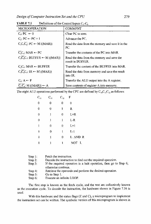
Design of Computer Instruction Set and the CPU 279
c,: PC - 0
TABLE 7.1 Definitions of the Control Inputs C,-C,
MICROOPERATION I COMMENT
Clear PC to zero.
C5GC,: BUFFER - M ((MAR))
C,C,: MAR - BUFFER
C,cC,: IR - M ((MAR))
C,: A +- F
C, C,: M ((MAR)) - A --
C , : P C - P C + 1 I Advance the PC.
Read the data from the memory and save the result in BUFFER.
Transfer the content of the BUFFER into MAR.
Read the data from memory and save the result into IR.
Transfer the ALU output into the A register.
Save contents of register A into memory.
C,C,G: PC - M ((MAR))
C,C,: MAR - PC -
Read the data from the memory and save it in the PC.
Transfer the contents of the PC into MAR.
Cl
0
0
0
0
1
1
1
1
Step 1: Step 2: Step 3:
Step 4: Step 5: Step 6:
1 c,, CI,
0 0
0 1
1 0
1 1
0 0
0 1
1 0
1 1
F
0
R
L+R
L-R
L+ 1
L- 1
L AND R
NOT L
Fetch the instruction. Decode the instruction to find out the required operation. If the required operation is a halt operation, then go to Step 6; otherwise continue. Retrieve the operands and perform the desired operation. Go to Step 1. Execute an infinite LOOP.
The first step is known as the fetch cycle, and the rest are collectively known as the execution cycle. To decode the instruction, the hardware shown in Figure 7.56 is used.
With this hardware and the status flags (Z and C), a microprogram to implement the instruction set can be written. The symbolic version of this microprogram is shown in

280 Fundamentals of Digital Logic and Microcomputer Design
(add&: 8-bit memory address in binary taddrH): 8-bit memory address in hex
MRI: memory reference instruction NMRI: nonmemory reference instruction.
FIGURE 7.54 Instruction Set to be Implemented
Figure 7.57. The hardware organization of the microprogrammed control unit for this situation
shown in Figure 7.58 directly follows the symbolic listing shown in Figure 7.57. No attempt has been made toward arriving at a minimal microprogram. Rather, the concept was presented. The task of translating the symbolic microprogram of Figure 7.57 into a binary microprogram is left as an exercise.

Design of Computer Instruction Set and the CPU 28 1
TC: GN:
Type classifier (if I3 = 1, then it is a MRI; otherwise it is Group number within a type
( I 2 I1 Group no.
0 0 0
0 1 1
1 0 2
1 1 3 1 SC: Subcategory within a group
FIGURE 7.55 Op-code Encoding Logic
a NMRI)
FIGURE 7.56 Instruction-decoding Hardware
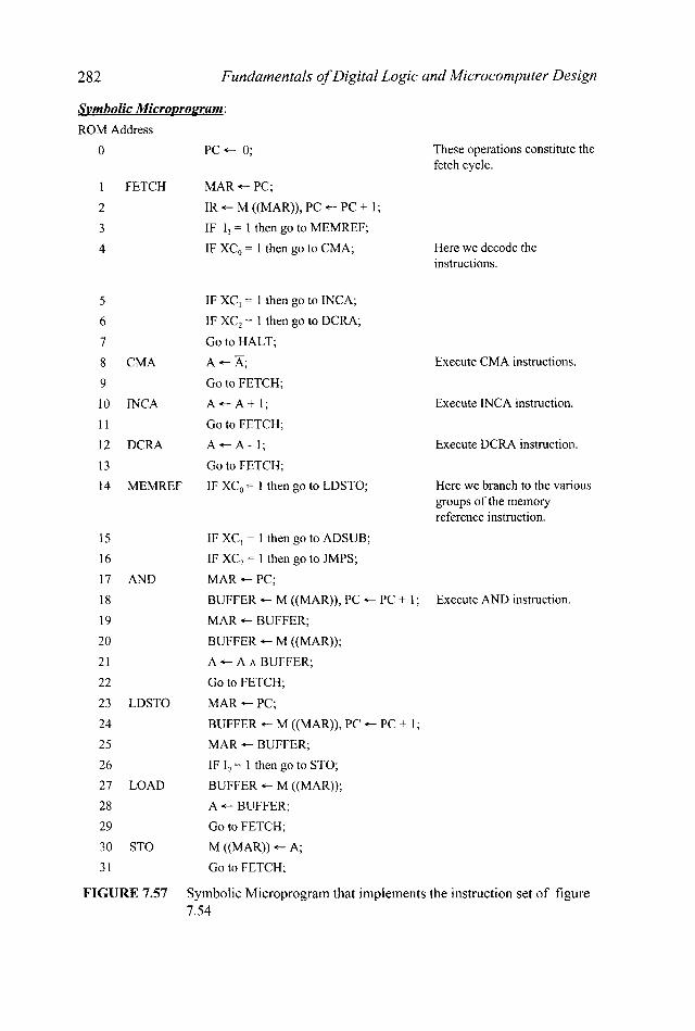
282 Fundamentals of Digital Logic and Microcomputer Design
Svmbolic MicroDrogram:
ROM Address
0
1 FETCH
2
3
4
5
6
7
8 CMA
9
10 INCA
1 1
12 DCRA
13
14 MEMREF
15
16
17 AND
18
19
20
21
22
23 LDSTO
24
25
26
27 LOAD
28
29
30 STO
31
PC- 0;
MAR - PC;
IR - M ((MAR)), PC - PC + 1;
IF 1, = 1 then go to MEMREF;
IF XC, = 1 then go to CMA;
IF XC, = 1 then go to INCA;
IF XC, = 1 then go to DCRA;
Go to HALT;
A - A; Go to FETCH;
A - A + l ;
Go to FETCH;
A - A - 1;
Go to FETCH;
IF XC, = 1 then go to LDSTO;
These operations constitute the fetch cycle.
Here we decode the instructions.
Execute CMA instructions.
Execute INCA instruction.
Execute DCRA instruction.
Here we branch to the various groups of the memory reference instruction.
IF XC, = 1 then go to ADSUB;
IF XC, = 1 then go to JMPS;
MAR - PC;
BUFFER - M ((MAR)), PC - PC + 1;
MAR + BUFFER;
BUFFER - M ((MAR));
A - A A BUFFER;
Go to FETCH;
MAR - PC;
BUFFER +- M ((MAR)), PC - PC + 1;
MAR - BUFFER;
IF I, = 1 then go to STO;
BUFFER + M ((MAR));
A + BUFFER;
Go to FETCH;
M ((MAR)) +- A;
Go to FETCH;
Execute AND instruction.
FIGURE 7.57 Symbolic Microprogram that implements the instruction set of figure 7.54

Design of Computer Instruction Set and the CPU
- 0 - Z - 1
C 2
13 3
xc2 4 MUX - xc 1 .5 xco - 6 10 7
"CL - 8
A Condition
select field Interpretation ,I 4
0000 No branch 0001 Branchif 2 1 001 0 Branch if C = 1 001 1 Branch if 13 = 1
283
4 Load16
MPC Reset
6
Control memory (52 x 33)
23
Condition Branch Control CMDB select address functions
J 6 4 c co c,,
32 ADSUB MAR-PC;
33
34 MAR - BUFFER ;
35 BUFFER 6 M ((MAR));
36 IF I, = 1 then go to SUB;
37 ADD A - A + BUFFER, Execute ADD instruction
38 Go to FETCH;
39 SUB A + A - BUFFER; Execute SUB instruction
40 Go to FETCH;
41 JMPS MAR - PC;
42
43
44 JOZ IF Z = 1 then go to LOADPC; Execute JZ instruction
BUFFER - M ((MAR)), PC + PC + 1 ;
IF I, = 1 then go to JOC;
IF I, = 1 then go to JOC;
45 P C - P C + l ;
46 Go to FETCH;
47 JOC IF C = 1 then go to LOADPC; Execute JC instruction
48 P C t P C + l ;
49 Go to FETCH;
50 LOADPC PC - M((MAR));
51 Go to FETCH;
52 HALT Go to HALT; Execute HALT instruction
FIGURE 7.57 Continued

284 Fundamentals of Digital Logic and Microcomputer Design
FIGURE 7.59 A microprogram of size A x B
Upper integer of
Microprogram Nanoprogram
Nanoprogram Control Memory
FIGURE 7.60 Nanomemory
O0 01
10
3 x 4 nanocontrol store
000 00 1 010 01 1 100 101 110
0100 El FIGURE 7.61 7 x 4-bit single control memory
000 00 1 010 01 1 100 101 110
7 x 2-bit mici rocontrol store
FIGURE 7.62 Two-level store (nanomemory) I t 9 4 I I+- 70 4
640 x 9
store 640 1 Microcontrol
FIGURE 7.63 68000 nanomemory

Design of Computer Instruction Set and the CPU
Example 7.1 If the following two instructions are to be added to the instruction set of Figure 7.54, write a symbolic microprogram for the CPU of section 7.3 that describes the execution of each
285
instruction:
GENERAL FORMAT
( 4 CLRA
(b) PRSA
OPERATION DESCRIPTION
A+O Clear register A
A+ 11 11 11 1 1 Set register A to all ones
Solution: (a) CLRA: A+O
(b) PRSA: A t 0 A+A go to FETCH
go to FETCH ; Use ALU’s zero output (C,,C,,C,,=OOO) 9
; Use ALU’s zero output (C,,C, ,C,,=OOO) ,
Nanomemory is another approach for reducing the size of the control memory. This technique contains a two-level memory: control memory and nanomemory. At the outset, are may feel that the two-level memory will increase the overall cost. In fact, it reduces the cost of the system by minimizing the memory size.
The concept of nanomemory is derived from a combination of horizontal and vertical instructions. However, this method provides trade-offs between them.
Motorola uses nanomemory to design the control units of their popular 16-bit and 32-bit microprocessors, including the 68000, 68020, 68030, and 68040. The nanomemory method provides significant savings in memory when a group of micro-operations occur several times in a microprogram. Consider the microprogram of Figure 7.59, which contains A microinstructions B bits wide. The size of the control memory to store this microprogram is AB bits. Assume that the microprogram has n (n < A ) unique microinstructions. These n microinstructions can be held in a separate memory called the “nanomemory” of size nB bits. Each of these n instructions occurs once in the nanomemory. Each microinstruction in the original microprogram is replaced with the address that specifies the location of the nanomemory in which the original B-bit-wide microinstructions are held.
Because the nanomemory has n addresses, only the upper integer of log,n bits is required to specify a nanomemory address. This is illustrated in Figure 7.60. The operation of microprocessor employing a nanomemory can be explained as follows: The microprocessor’s control unit reads an address from the microprogram. The content of this address in the nanomemory is the desired control word. The bits in the control word are used by the control unit to accomplish the desired operation. Note that a control unit employing nanomemory (two-level memory) is slower than the one using a conventional control memory (single memory). This is because the nanomemory requires two memory reads (one for the control memory and the other for the nanomemory). For a single conventional control memory, only one memory fetch is necessary. This reduction in control unit speed is offset by the cost of the memory when the same microinstructions occur many times in the microprogram.
Consider the 7 x 4-bit microprogram stored in the single control memory of Figure 7.61. This simplified example is chosen to illustrate the nanomemory concept even though this is not a practical example. In this program, 3 out of 7 microinstructions are unique.

286 Fundamentals of Digital Logic and Microcomputer Design
Therefore, the size of the microcontrol store is 7 x 2 bits and the size of the nanomemory is 3 x 4 bits. This is shown in Figure 7.62.
Memory requirements for the single control memory = 7 x 4 = 28 bits. Memory requirements for nanomemory = (7 x 2 + 3 x 4) bits = 26 bits. Therefore, the saving using nanomemory = 28 - 26 = 2 bits. For a simple example like this, 2 bits are saved. The HMOS 68000 control unit nanomemory includes a 640 x 9-bit microcontrol store and a 280 x 70-bit nanocontrol store as shown in Figure 7.63. In Figure 7.63, out of 640 microinstructions, 280 are unique. If the 68000 were implemented using a single control memory, the requirements would have been 640 x 70 bits. Therefore,
Memory savings = (640 x 70) - (640 x 9 + 280 x 70) bits
= 19,440 bits = 44,800 - 25,360
This is a tremendous memory savings for the 68000 control unit.
DUESTIONS AND PROBLEMS
7.1
7.2
7.3
7.4
7.5
7.6
It is desired to implement the following instructions using block code: ADD, SUB, XOR, MOVE, HALT. Draw a block diagram.
The instruction length and the size of an address field are 9 bits and 3 bits respectively. Is it possible to have
6 two-address instructions 15 one-address instructions 8 zero-address instructions
using expanding op-code technique? Justify your answer.
Using the instruction format of Problem 7.2, is it possible to have 7 two-address instructions 7 one-address instructions 8 zero-address instructions
using expanding opcode technique? Justify your answer.
Assume that it is desired to have 2 two-address, 7 one-address, and 25 zero- address instructions in a computer instruction set. Using expanding op-code technique with a 2-bit op-code and 3-bit address field, is it possible to accomplish the above? If so, justify your answer and determine the instruction length.
Assume that using an instruction length of 9 bits and the address field size of 3 bits, 5 two-address and 10 one-address instructions have already been designed, using expanding op-code technique. Is it possible to have at least 48 zero-address instructions that can be added to the instruction set?
Design a combinational logic shifter with 4-bit input and 4-bit output as follows:

- OE
1 0 0 0 0
7.7
7.8
7.9
7.10
7.1 1
7.12
7.13
Shift Count 4 - bit output
s, so X X High Impedance output lines 0 0 No Shift 0 1 Right Shift once 1 0 Right Shift twice 1 1 Right Shift three times
where X means don’t care. Using multiplexers and tristate buffers, draw a logic diagram.
Draw a logic diagram for a 4 x 4 barrel shifter.
Using a minimum number of full adders and multiplexers, design an incremented decrementer circuit as follows: If S = 0, output y = x + 1 ; otherwise, y = x - 1. Assume x and y are 4-bit signed numbers and the result is 4 bits wide.
Design a combinational circuit to compute the absolute value of an 8-bit twos complement number. Use %bit binary adder and exclusive-OR gates. Draw a logic circuit.
Using a 4-bit CLA as the building block, design an 8-bit adder.
Design: (a)
(b)
(c)
a 16-bit adder whose worst-case add-time is 10A using a 4-bit CLA as a building block. the fastest 64-bit adder using a 4-bit CLA as the building block. Estimate the worst-case add-time of your design. a combinational circuit to compute the fimctionf(x) = (3/8) * x where x is a 4-bit 2’s complement number.
Design an arithmetic logic unit to perform the following hnctions:
A minus B A AND B A O R B
Use multiplexers, binary adders, and gates as needed. Assume that A and B are 4-bit numbers. Draw a logic circuit.
Design a combinational circuit that will perform the following operations:
B 15
288
7.14
Fundamentals of Digital Logic and Microcomputer Design _--_
Assume that A is a 4-bit number and B = u3 a, a , a,. Draw a logic diagram.
Design a 4-bit ALU to perform the following operations:
S F 0 1 0
Logical Left Shift A once
7.15
7.16
7.17
7.18
7.19
7.20
7.2 1
7.22
Assume that A is a 4-bit number. Draw a logic diagram using a binary adder, multiplexers, and inverters as necessary.
Design a 4-bit arithmetic unit as follows:
S I F A plus B
Assume that A and B are 4-bit numbers
Design an ALU to perform the following operations:
O B XO
_ _ _ _ Assume that x and y are 4-bit numbers, and B= y3 y , y , y,. Draw a logic diagram.
Assume two 2’s complement signed numbers, M = 1 1 1 1 1 1 1 1 , and Q = 1 1 1 1 1 100,. Perform the signed multiplication using the algorithm described in Section 7.2.2.
What is the purpose of the control unit in a microprocessor?
Draw a logic diagram to implement the following register transfers: (a) If the content of the 8-bit register R is odd, then
x + x o y else x+ x AND y
Assume x and y are 4 bits wide. (b) If the number in the 8-bit register R is negative, then x + x - 1 else x -
x + 1. Assume x and y are 4 bits wide.
Discuss briefly the merits and demerits of single-bus, two-bus, and three-bus architectures inside a control unit.
What is the basic difference between hardwired control, microprogramming, and nanoprogramming? Name the technique used for designing the control units of the Intel 8086, Motorola 68000, and PowerPC.
Using the following components: 4-bit general-purpose register, 4-bit adderhubtractor, and tristate buffer, and assuming the inbus and outbus are
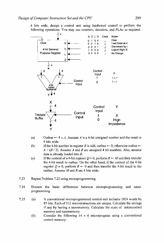
Design of Computer Instruction Set and the CPU 289
4 bits wide, design a control unit using hardwired control to perform the following operations. You may use counters, decoders, and PLAs as required.
I
Clock R 4
4-bit General c Purpose Register
~
7.23
7.24
7.25
4
D-
1
F 4 4
X ,L-4
Control Input
t Y
R C L D Clock
0 1 0 0 1 0 0 1 0 1 0 0 0 1 1 1 0 0 0 .J 0 0 0 0 .J
Control Input
1
0
Control Input
1 0
Action Clear Load External d Decrement by ( Logical Right Sl No Change
F I + r I - r
Y
X High
lmpedence
(a)
(b)
Outbus - 4 x A . Assume A is a 4-bit unsigned number and the result is 4 bits wide. If the 4-bit number in register B is odd, outbus +- 0; otherwise outbus - A + ( B I 2). Assume A and B are unsigned 4 bit numbers. Also, assume data is already loaded into B. If the content of a 4-bit register Q = 0, perform R + M and then transfer the 4-bit result to outbus. On the other hand, if the content of the 4-bit register Q # 0, perform R - 0 and then transfer the 4-bit result to the outbus. Assume M and R are 4 bits wide.
(c)
Repeat Problem 7.22 using microprogramming.
Discuss the basic differences between microprogramming and nano- programming.
(a) A conventional microprogrammed control unit includes 1024 words by 85 bits. Each of 5 12 microinstructions are unique. Calculate the savings if any by having a nanomemory. Calculate the sizes of microcontrol memory and nanomemory. Consider the following 14 x 6 microprogram using a conventional control memory:
(b)

290
s1
1
Fundamentals of Digital Logic and Microcomputer Design
so Y,
0 1 4 0 0 0 Circuit
- o x , so
1 1 1
0000 000 1 0010 001 1 0100 0101 01 10 0111 1000 1001 1010 101 1 1100 1101 1110
000001 00001 1 0000 10 00001 1 0000 1 0 B 000001
Implement this microprogram in a nanomemory. Justify the use of either a single- control memory or a two-level memory for the program.
7.26 Discuss the basic differences between CISC and RISC.
7.27 Design and implement a combinational circuit that will work as follows:
Shift left A A lus B lus 1
1 Shift left A + 1 Note that A and B are 4-bit operands
7.28 i) Design a combinational circuit that will satisfy the following specification.
ii) Using the results of part i), design a 4-bit, 8-function arithmetic unit ii) will function as described next:
A plus B 0 A plus
that
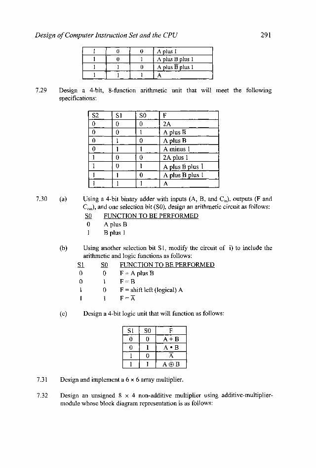
Design of Computer Instruction Set and the CPU
1 1 1
29 1
0 1 A plus B plus 1 1 0 A plus B plus 1 1 1 A
1 1 1 0 1 0 I A plus 1 I
0 l o 1 1 0 1 1 l o
A plus E A plus B
7.29 Design a 4-bit, 8-function arithmetic unit that will meet the following specifications:
1 1 1 1
s 2 I s 1 I so I F 0 l o l o I 2A
0 0 2Aplus 1 0 1 A plus B plus 1 1 0 A plus B plus 1 1 1 A
I o I 1 I 1 I ~ m i n u s 1 I
(b) Using another selection bit S1, modify the circuit of i) to include the arithmetic and logic functions as follows: - s1 - SO FUNCTION TO BE PERFORMED 0 0 F = A p l u s B 0 1 F - B 1 0 F = shift left (logical) A 1 1 F = A
(c) Design a 4-bit logic unit that will function as follows:
7.3 1 Design and implement a 6 x 6 array multiplier.
7.32 Design an unsigned 8 x 4 non-additive multiplier using additive-multiplier- module whose block diagram representation is as follows:

292 Fundamentals of Digital Logic and Microcomputer Design
M Q
1 P - M.0- Y
Assume that M, Q, and Y are unsigned integers.
7.33 Using four 256 x 8 ROMS and 4-bit parallel adders, design a 8 x 8 unsigned, nonadditive multiplier. Draw a logic diagram of your implementation.
7.34 Consider the registers and ALU shown in Figure P7.34:
C, -
Load 8
The intemretation of various control points are summarized as follows:
R minus S A + F R and S R EX-OR
FIGURE P7.34
Answer the following questions by writing suitable control word(s). Each control word must be specified according to the following format: C, C , C2 C, Co For example:
c4 c3 c2 c, co 1 0 0 0 1 ; A - A p l u s B

Design of Computer Instruction Set and the CPU 293
(a)
(b)
How will the A register be cleared? (Suggest at least two possible ways.) DIRECT CLEAR input is not available. Suggest a sequence of control words that exchanges the contents of A and B registers (exchange means A .E- B and B -+ A).
7.35 Consider the following algorithm: Declare registers A [8], B [8], C [8]; START: A - 0; B * 0000 10 10; LOOP: A + A + B; B + B - 1;
If B < > 0 then go to LOOP C c- A;
HALT: Go to HALT Design a hardwired controller that will implement this algorithm.
7.36 It is desired to build an interface in order establish communication between a 32- bit host computer and a front end 8-bit microcomputer (See Figure P7.36). The operation of this system is described as follows: Step 1: First the host processor puts a high signal on the line “want” (saying that
it needs a 32-bit data) for one clock period. Step 2: The interface recognizes this by polling the want line. Step 3: The interface unit puts a high signal on the line “fetch” for one clock
period (that is it instructs the microcomputer to fetch an 8-bit data). Step 4: In response to this, the microcomputer samples the speech signal,
converts it into an 8-bit digital data and informs the interface that the data is ready by placing a high signal on the “ready” line for one clock period.
Step 5: The interface recognizes this (by polling the ready line), and it reads the 8-bit data into its internal register.
.Step 6: The interface unit repeats the steps 3 through 5 for three more times (so that it acquires 32-bit data from the microcomputer).
Step 7: The interface informs the host computer that the latter can read the 32-bit data by placing a high signal on the line “takeit” for one clock period.
Step 8: The interface unit maintains a valid 32-bit data on the 32-bit output bus until the host processor says that it is done (the host puts a high signal on the line “done” for one clock period). In this case, the interface proceeds to step 1 and looks for a high on the “want” line.
(a) (b) (c) (d)
Provide a Register Transfer Language description of the interface. Design the processing section of the interface. Draw a block diagram of the interface controller. Draw a state diagram of the interface controller.
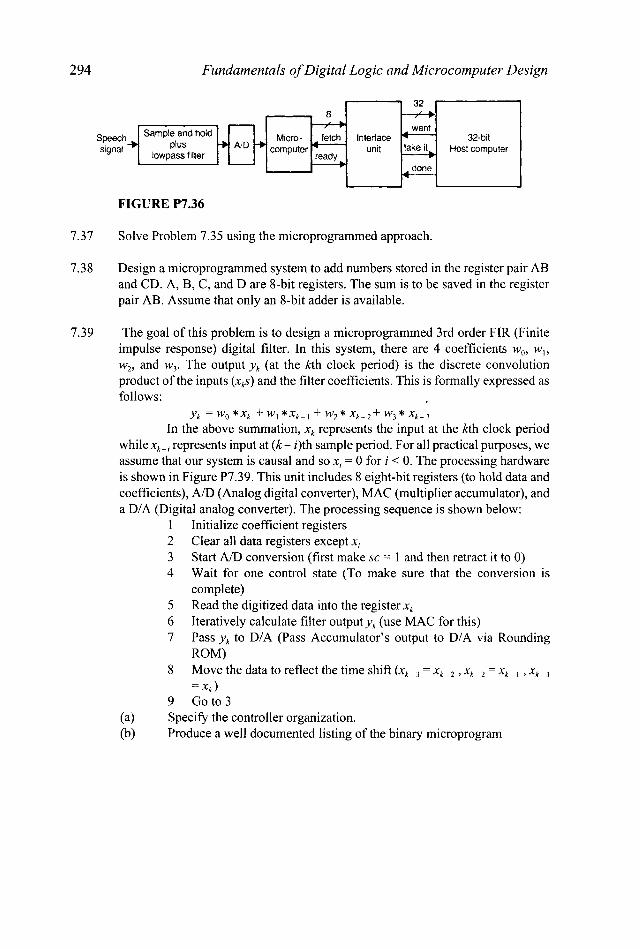
294
Speech Sample and hold
signat -* plus lowpass titter
-*
Fundamentals of Digital Logic and Microcomputer Design
want Micro- fetch Interface +-- 32-blt
-* computer t-
7.37 Solve Problem 7.35 using the microprogrammed approach.
7.38 Design a microprogrammed system to add numbers stored in the register pair AB and CD. A, B, C, and D are 8-bit registers. The sum is to be saved in the register pair AB. Assume that only an 8-bit adder is available.
7.39 The goal of this problem is to design a microprogrammed 3rd order FIR (Finite impulse response) digital filter. In this system, there are 4 coefficients w,, w,, w,, and w3. The output y , (at the kth clock period) is the discrete convolution product of the inputs ( x ~ ) and the filter coefficients. This is formally expressed as follows:
y , = wg *x, + WI *xk-1 + w2* x,-2+ w,* Xk-3 In the above summation, x, represents the input at the kth clock period
while xk-, represents input at (k- i)th sample period. For all practical purposes, we assume that our system is causal and so xi = 0 for i < 0. The processing hardware is shown in Figure P7.39. This unit includes 8 eight-bit registers (to hold data and coefficients), N D (Analog digital converter), MAC (multiplier accumulator), and a D/A (Digital analog converter). The processing sequence is shown below:
1 Initialize coefficient registers 2 3 4
5 6 7
Clear all data registers except x, Start N D conversion (first make sc = 1 and then retract it to 0) Wait for one control state (To make sure that the conversion is complete) Read the digitized data into the register x, Iteratively calculate filter output y, (use MAC for this) Pass y , to D/A (Pass Accumulator’s output to D/A via Rounding ROM)
8 Movethedatatoreflectthetimeshift(x,_,=x,_, , X ~ . ~ - X , - ~ -
9 G o t 0 3 (a) Specify the controller organization. (b) Produce a well documented listing of the binary microprogram

Design of Computer Instruction Set and the CPU 295
sc (slan mnverston)
AnalDg
(mnicient databus)
dm (data move)
(dala dear)
Deader
i-' I I I I I l l I I
le (baa enable)
I I- - I I
I
I- L - - - - - - - - - - - - - - -
filter
I I I I I I I I I I I I I I
Rounding
16
? MAC
FIGURE P7.39
7.40 Your task is to design a microprogrammed controller for a simple robot with 4 sensors (see Fig. A). The sensor output will go high only if there is a wall or an obstruction within a certain distance. For example, if F= 1, there is an obstruction or wall in the forward direction. In particular, your controller is supposed to communicate with a motor controller unit shown in Fig. B. The flow chart that describes the control algorithm is shown in Fig. C. The outputs such as MFTS, MRT, MLT, MUT, and STP, andd the status signals such as FMC, and TC will be high for one clock period. Assume that a power on reset causes the controller to go the WAIT STATE 0.
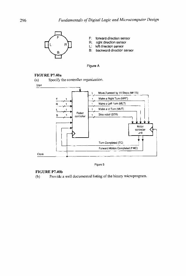
296
F 1
R 1
L ,1 * B 1
Fundamentals of Digital Logic and Microcomputer Design
1
1
I Make a U-Turn (MUT)
Make a Right Turn (MRT)
Make a Left Turn (MLT) -
Robot 1 Stop robot(STR)
1
F: forward direction sensor R: right direction sensor L: left direction sensor B: backward direction sensor
Figure A
FIGURE P7.40a (a) Specify the controller organization.
Stan
Clock
$ 4 4 4 4 Motor
controller unit
Turn Completed (TC)
Fonvard Motion Completed (FMC)
Figure 0
FIGURE P7.40b (b) Provide a well documented listing of the binary microprogram.

Design of Computer Instruction Set and the CPU 297
MFTS = 1 b No
No A MRT = 1
1r MLT = 1
L r
I’
STP = 1 9 Wait slate 6-
-7i Wait slate
+J$ = l ?
L . r
Figure C
FIGURE P7.40~
7.41 It is desired to add the following instructions to the instruction set shown in Figure 7.54.
(a) MVIA tdata8) A 6 (data% This is an immediate mode move GENERAL FORMAT OPERATION DESCRIPTION
instruction. The first byte contains the op-code while the second byte contains the 8- bit data.
(b) NEGA A + - A This instruction negates the contents o f A
Write a symbolic microprogram that describes the execution of each instruction.
7.42 Explain how the effect of an unconditional branch instruction of the following form is simulated: JP taddri
298 Fundamentals of Digital Logic and Microcomputer Design
Use the instruction set shown in Figure 7.54.
7.43 Using the instruction set shown in Figure 7.54, write a program to add the contents of the memory locations 64,, through 6D,, and save the result in the address 6%
7.44 Show that it is possible to specify 675 microoperations using a 10 bit control function field.
7.45 A microprogram occupies 100 words and each word typically emits 70 control signals. The architect claims that by using a 2’ x 70 nanomemory (for some i > 0), it is possible to save 4260 bits. If this were true, determine the number of distinct control states in the original microprogram (Note that here when we say a control state we refer only to the control function field). Hint: You may have to employ a trial and error approach to solve this problem.