Embed Size (px)
Citation preview
Turk J Elec Eng & Comp Sci
(2016) 24: 2806 – 2824
c⃝ TUBITAK
doi:10.3906/elk-1404-174
Turkish Journal of Electrical Engineering & Computer Sciences
http :// journa l s . tub i tak .gov . t r/e lektr ik/
Research Article
Design of compact octagonal slotted hexagonal and rectangular shaped monopole
antennas for dual/UWB applications
Praveen Naidu VUMMADISETTY1, Raj KUMAR2,∗
1Department of Electronics and Telecommunication, Symbiosis International University, Pune, India2Department of Armament Electronics, Armament Research and Development Establishment, Pashan, Pune, India
Received: 10.04.2014 • Accepted/Published Online: 06.12.2014 • Final Version: 15.04.2016
Abstract: Two CPW-fed compact printed slot antennas for UWB applications are proposed in this paper. In both
antennas, the slot in the ground plane is of octagonal shape, while the patch is rectangular in one of the antennas and
hexagonal in the other. Thin metallic stubs of different lengths are added to the ground plane and protrude into the
slot. These stubs help to improve the impedance matching over a broader bandwidth. The antennas are very compact
in size and designed on low-cost FR4 substrate. The measured impedance bandwidths (S11 < –10 dB) achieved by the
rectangular and hexagonal patch antennas are from 3.1 GHz to 5.6 GHz and 3.14 GHz to 5.34 GHz, respectively. The slot
antenna with hexagonal patch is further modified to have dual-band characteristics. An L-shaped stub is attached to the
ground plane to achieve an additional band from 2.45 GHz to 2.52 GHz for WLAN applications. The radiation patterns
of the antennas are dumb-bell shape in the E-plane and omnidirectional in the H-plane. Detailed parametric studies of
the antennas have been carried out. The simulated results are found to be in good agreement with the measured results.
Key words: CPW-fed antenna, monopole antenna, ultrawideband antenna
1. Introduction
In 2002, the Federal Communications Commission (FCC) had allotted a frequency spectrum range from 3.1
GHz to 10.6 GHz for unlicensed ultrawideband (UWB) communications (https://transition.fcc.gov/Bureaus/
Engineering Technology/Orders/2002/fcc02048.pdf). After that, many researchers have paid attention to the
design of compact antennas for UWB. There are two standard approaches for UWB systems, i.e. DS-CDMA
(direct-sequence code division multiple access) and MB-OFDM (multiband orthogonal frequency division multi-
plexing). The DS-CDMA approach divides the full band into three modes of operation, i.e. a low band consisting
of frequencies ranging from 3.1 GHz to 5.15 GHz, a high band consisting of frequencies ranging from 5.82 GHz
to 10.6 GHz, and a multiband or mixed band consisting of frequencies ranging from 3.1 GHz to 10.6 GHz.
MB-OFDM divides the full band of 3.1 GHz to 10.6 GHz into 14 subbands, each with a bandwidth of 528 MHz,
and each subband is composed of 128 tones and is modulated using OFDM. The lower three subbands (3.168
GHz to 4.752 GHz) are decided as mandatory mode (Group A) in the MB-OFDM system, which can provide
more than 100 Mbps data rate (IEEE Document P802.15-03/268r1, September 2003; https://www.ieee.org/).
As shown in Figure 1, Group A has three channels, 3168–3696 MHz (Channel 1), 3696–4224 MHz (Channel 2),
and 4224–4752 MHz (Channel 3).
∗Correspondence: [email protected]
2806

VUMMADISETTY and KUMAR/Turk J Elec Eng & Comp Sci
3.432 3.960 4.488 5.016 5.806 f (GHz)
Power
level
UWB MB-OFDM Group A
UWB MB-OFDM Group B
Hiperlan
5.125-5.325 GHz
IEEE 802.11a
5.725-5.825 GHz
Maximum power allotted
-41.3 dBm/MHz
DS-CDMA lower band 3.1-5.15 GHz
528 MHz
Figure 1. Frequency band of MB-OFDM and DS-CDMA.
To implement the MB-OFDM/DS-CDMA approach, UWB antennas of compact size, omnidirectional
radiation patterns, and constant gain are required. Recently many researchers have reported UWB antennas
[1–22] for MB-OFDM/low-band DS-CDMA systems with a frequency range of 3.1 GHz to 4.8 GHz/3.1 GHz to
5.15 GHz. In [1], a compact 20 mm × 30 mm tree shaped fractal UWB antenna was presented for MB-OFDM
lower three band (3.1–4.8 GHz) applications. A 26 mm × 41.8 mm coplanar waveguide (CPW)-fed balanced
wideband dipole antenna was proposed for 3-7 GHz UWB applications in [2]. A compact 30 mm × 30 mm
filter combined UWB antenna for 3.1 GHz to 5.2 GHz DS-CDMA/MB-OFDM applications was proposed in [3].
A CPW-fed, pentagonal cut fractal antenna (31 mm × 32 mm) was presented in [4] for 4.69 GHz to 15 GHz
DS-CDMA higher band applications. A compact 30 mm × 20 mm monopole antenna with two symmetrical
strips for 3.1–4.8 GHz frequency band operation was proposed in [5]. In [6] a 50 mm × 67 mm diamond shaped
fractal antenna was designed using the CPW-fed technique for UWB applications with frequency range from 2.0
GHz to 6.2 GHz. A U-shaped open stub CPW-fed antenna was proposed in [7] for dual frequency applications.
The proposed design has overall dimensions of 35 mm × 30 mm and works for 2.4 GHz WLAN and 3.0 GHz to
6.0 GHz UWB applications. Similarly, various monopole antennas were reported in [8–11] for 3.0 GHz to 5.15
GHz frequency operation but these antennas have the drawback of larger size in comparison with our proposed
designs. Various dual-band antennas were also presented in [12–15]. In [12], a 25 mm × 25 mm microstrip-fed
antenna was proposed for dual frequency band applications. By using a meander in the ground plane, lower
frequency at 2.44 GHz was generated, and by using an L-shaped radiator higher resonance frequency at 5.8 GHz
was achieved. Similarly, for achieving dual-band operation a bow-tie shaped slot in [13], U-shaped slot in [14],
and rectangular slot in [15] were used in the antenna design. A 120 mm × 100 mm slot antenna was proposed
in [16] by using the microstrip-feeding technique. For achieving an UWB from 3.1 GHz to 10.6 GHz a square
ring slot was introduced in the structure. Various slot antennas with different dimensions were reported in
[17–22] for WLAN/UWB applications. A comparison study of all the UWB and dual-band antennas mentioned
in references [1–21] in terms of overall size and bandwidth achieved is given in Table 1. Though some of the
referenced antennas cover the entire UWB band, those antennas have the drawback of large dimensions. As a
result, it is very difficult to integrate the antenna with other RF and MIMO circuits.
In this paper, two compact CPW-fed octagonal slot antennas with hexagonal and rectangular shaped
patches are designed. These antennas have bandwidths of 2.5 GHz (3.10–5.6 GHz) and 2.20 GHz (3.14–5.34
GHz), respectively. In addition, an UWB and dual-band antennas are also presented in Sections 7 and 8. These
designs offer an extended bandwidth up to 9.2 GHz (3.1 GHz to 12.3 GHz) in the case of UWB antenna design
and an additional band centered at 2.5 GHz in the case of dual-band antenna design, respectively. All the
2807

VUMMADISETTY and KUMAR/Turk J Elec Eng & Comp Sci
above designed antennas have more compact size (20 mm × 20 mm) compared to the reference antennas. The
antennas are designed, simulated, and optimized using CST Microwave Studio 3D-electromagnetic software and
validated experimentally. The proposed antennas can be used for DS-CDMA/MB-OFDM (Group A) UWB
systems.
Table 1. Comparison of the proposed antenna with reference antennas.
Serial. no. No Reference Antenna type Size (mm × mm) Operating band1. Ref [1] UWB 30 × 20 3.1–4.8 GHz2. Ref [2] UWB 26 × 41.8 3.1–4.8 GHz3. Ref [3] UWB 30 × 30 3.1–5.2 GHz4. Ref [4] UWB 31 × 32 4.69–15 GHz5. Ref [5] UWB 30 × 20 3.1–4.8 GHz6. Ref [6] UWB 50 × 67 2.0–6.2 GHz7. Ref [7] Dual-band 35 × 30 2.45 GHz & 3–6 GHz8. Ref [8] UWB 40 × 100 3.1–5.15 GHz9. Ref [9] UWB 24 × 25 3.1–5.1 GHz10. Ref [10] UWB 20 × 30 3.1–4.8 GHz11. Ref [11] UWB 24 × 25 3.1–5.1 GHz12. Ref [12] Dual band 25 × 25 2.38–2.51 GHz & 4.79–5.98 GHz13. Ref [13] Dual-band 60 × 45 2.26–2.57 GHz & 4.81–6.56 GHz14. Ref [14] Dual-band 40 × 40 2.4–2.484 GHz & 5.15–5.825 GHz15. Ref [15] Dual-band 75 × 75 2.4 GHz & 5 GHz16. Ref [16] Single-band 120 × 100 3.1–10.6 GHz17. Ref [17] Single-band 45 × 21.5 3.0–10 GHz18. Ref [18] Single-band 85 × 85 2.8–14 GHz19. Ref [19] Single-band 66.1 × 44 3.1–12 GHz20. Ref [20] Single-band 90 × 90 4.71–6.14 GHz21. Ref [21] Single-band 100 × 100 3.1–10.6 GHz22. Proposed antenna Dual band 20 × 20 2.5 GHz & 3.0–6.0 GHz
2. Antenna structure
The geometries of the proposed antennas are shown in Figure 2. The antennas are designed on FR-4 substrate
having thickness of 1.58 mm and permittivity of 4.3. The ground plane is printed on one side of the substrate.
An octagonal slot is etched on the ground plane for both antennas. The radiating element is a hexagonal
patch for one of the antennas and a two-stepped rectangular patch for the other. The hexagonal patch’s height
(denoted by ‘g10’ in Figure 2a) gives higher cut-off frequency near 5.15 GHz while the hexagonal patch’s width
‘g9’ is optimized to get the best return loss characteristic. Another parameter in the design that has to be
optimized to ensure good return loss performance is the vertical separation between the patch and the ground
plane. This parameter is denoted by ‘g5’ and its optimal value is found to be equal to 3 mm. For the rectangular
patch antenna, the patch’s height, ‘g13’ (Figure 2b), gives the higher cut-off frequency near 5 GHz, while the
patch’s width, ‘g8’, is optimized to get the best return loss characteristic. Three vertical stubs are added to the
octagonal shaped ground section for better impedance matching. The vertical separation between the patch
and the lower ground plane is denoted by ‘b10’ and its optimal value is found to be equal to 3.5 mm. The
dimensions of all the parameters of the two antennas are listed in Tables 2 and 3, respectively.
Figure 3 shows the different stages in the design of the proposed hexagonal patch antenna and the
corresponding reflection coefficients are shown in Figure 4. The initial design (Antenna #1a) as seen in Figure
2808
VUMMADISETTY and KUMAR/Turk J Elec Eng & Comp Sci
L
W
b8
b1
b2b2
b12g3
b1
b7
g1
b9
b3
g4
b11b10
b6
b5 b5g6
g2g5 b4
g8
g9
g7
g10
g11
x
y
z
Figure 2. a)Proposed hexagonal patch antenna.
b7
b3
L
W
b5 b5
g1
b2b8g3
b2
b1 b1
g10
b12
g4
g12
g11
b6
b10
g2
g
b9
b11b4
g9
g8
g7
g13
g5
g6
x
y
z
Figure 2. b) Proposed rectangular patch antenna.
Table 2. Optimal parameters of the proposed hexagonal patch antenna.
Parameter W L b1 b2 b3 b4 b5 b6 b7 b8Value (mm) 20 20 11 4.2 10 2.5 4.3 2.5 1 0.5Parameter b9 b10 b11 b12 g1 g2 g3 g4 g5 g6Value (mm) 1 3 3.1 4 0.4 0.2 2 1.5 3 2Parameter g7 g8 g9 g10 g11Value (mm) 3 7 12 6 3.9
3 consists of a hexagonal shaped patch surrounded by octagonal shaped slot etched on the ground plane and
excited by a 50 Ω CPW feed line. To enhance the impedance bandwidth, the initial design is modified and
the modified versions are named Antenna #2a, Antenna #3a, and proposed antenna. It can be seen in Figure
4 that there is an improvement in the impedance bandwidth along with enhanced impedance matching with
successive modifications in the design.
2809
VUMMADISETTY and KUMAR/Turk J Elec Eng & Comp Sci
Table 3. Optimal parameters of the proposed rectangular patch antenna.
Parameter W L b1 b2 b3 b4 b5 b6 b7 b8Value (mm) 20 20 11 3.6 12 2.8 4.3 2.8 1.5 4Parameter b9 b10 b11 b12 g1 g2 g3 g4 g5 g6Value (mm) 3 3.7 2 5 0.5 0.4 0.4 0.5 0.8 1.7Parameter g7 g8 g9 g10 g11 g13 g12 gValue (mm) 2.6 6.8 4.8 4.6 1.5 5.5 1.8 1.0
Antenna #1(a) Antenna #2(a) Antenna #3(a) Proposed antenna
Figure 3. Different stages of the proposed hexagonal patch antenna.
2 2.35 2.7 3.05 3.4 3.75 4.1 4.45 4.8 5.15 5.5 5.85 6.2 6.5–60
–50
–40
–30
–20
–10
0
Frequency (GHz)
S11
(d
B)
Antenna #1(a)Antenna #2(a)Proposed AntennaAntenna #3(a)
Figure 4. Simulated S11 for different stages of hexagonal patch antenna.
The initial designs of the rectangular patch antenna along with the modified versions are shown in Figure
5. The simulated reflection coefficients are shown in Figure 6. The slot used is similar to that of the hexagonal
patch antenna. However, the tuning stubs are shaped differently. Again it can be seen in Figure 6 that there
is an improvement in the impedance bandwidth with successive addition of rectangular shaped stubs in the
design.
3. Measured and simulated results
The proposed two antennas (hexagonal patch and rectangular patch) are designed and fabricated with optimized
dimensions. Figures 7 and 8 show the fabricated prototypes of the hexagonal and rectangular patch antennas
along with their measured and simulated reflection coefficients. The measurements were performed using
a Rohde & Schwarz Vector Network Analyzer (R&S ZVA-40). The measured impedance bandwidth of the
2810

VUMMADISETTY and KUMAR/Turk J Elec Eng & Comp Sci
octagonal slotted rectangular patch antenna is 2.5 GHz from 3.10 GHz to 5.6 GHz and that of the hexagonal
patch antenna is 2.20 GHz from 3.14 GHz to 5.34 GHz. It can be seen in the figures that the measured and
simulated reflection coefficients are in good agreement. The slight difference between the measured and simulated
results is due to fabrication constraints, uncertainties in the dielectric constant and substrate thickness, soldering
effects, and the quality of the SMA connector used.
Antenna #1 Antenna #2
Antenna #3
Proposed antenna
Figure 5. Different stages of the proposed rectangular patch antenna.
2 2.5 3 3.5 4 4.5 5 5.5 6 6.5–50
–45
–40
–35
–30
–25
–20
–15
–10
–5
0
Frequency (GHz)
Ret
urn
Lo
ss (
dB
)
Antenna #1
Antenna #2Antenna #3Proposed Antenna
Figure 6. Simulated S11 for different stages of the proposed rectangular patch antenna.
2.5 2.9 3.3 3.7 4.1 4.5 4.9 5.3 5.7 6–60
–50
–40
–30
–20
–10
0
Frequency (GHz)
S1
1 (
dB
)
Simulated (Hexagonal patch Antenna)Measured (Hexagonal patch Antenna)
Figure 7. Photograph of the proposed hexagonal patch antenna with the corresponding simulated and measured return
loss.
2811

VUMMADISETTY and KUMAR/Turk J Elec Eng & Comp Sci
2.5 2.8 3.1 3.4 3.7 4 4.3 4.6 4.9 5.2 5.5 5.8 6.1 6.4 6.6–45
–40
–35
–30
–25
–20
–15
–10
–5
0
Frequency (GHz)
S1
1 (
dB
)
Simulated Measured
Figure 8. Photograph of the proposed rectangular patch antenna with the corresponding simulated and measured
return loss.
4. Theoretical analysis
The contributing factor for the first resonance (fH1 = 3.46 GHz and fR1 = 3.25 GHz) seen in the simulated
S11 curves (Figures 7 and 8) of the proposed hexagonal and rectangular patch antennas is due to the octagonal
slot perimeter. The resonance frequencies for these two antennas are approximately obtained from Eqs. (1)
and (2). The second resonances (near 5.15 GHz and 5.05 GHz) are due to the patch height and also affected
by the coupling between the lower edge of the patch and the upper edge of the ground plane. As given in [23],
the second resonance frequencies are obtained from Eqs. (3) and (4).
fH1 =C
l1√εr,eff
(1)
fR1 =C
L1√εr,eff
(2)
f2 =C
4l2√εr,eff
(3)
f3 =C
4l3√εr,eff
(4)
l1 + L1 = 2b1 + 2b2 + b3 + b4 + 2b5 + b6 (5)
l2 = g5 + g10 (6)
l3 = b10 + g13 (7)
L2+H7+H10+H11+H12+H13+H14+H15+H16εr,eff =εr + 1
2(8)
2812

VUMMADISETTY and KUMAR/Turk J Elec Eng & Comp Sci
Here, c stands for the velocity of light in free space; l1 and L1 are the slot perimeters of the hexagonal and
rectangular patch antennas, respectively; and l2 and l3 are the effective monopole heights of hexagonal and
rectangular patch antennas, respectively, while εr,eff is the effective relative permittivity to be calculated using
Eq. (8). For calculating the effective relative permittivity, it is assumed that for a CPW-fed monopole, half of
the established field lies in the air while the remaining half is distributed in the substrate. The first and second
resonance frequencies are calculated using Eqs. (1)–(8). Table 4 shows the comparison between calculated and
simulated resonance frequencies.
Table 4. Comparison between calculated and simulated resonances.
Resonance frequency Calculated value Simulated valuefH1 (hexagonal patch, first resonance) 3.39 GHz 3.46 GHzfR1 (rectangular patch, first resonance) 3.30 GHz 3.25 GHzf2 (hexagonal patch, second resonance) 5.08 GHz 5.17 GHzf3 (rectangular patch, second resonance) 4.98 GHz 5.05 GHz
The return loss or resonance frequency characteristics of the hexagonal and rectangular shaped patch
antennas can also be explained by observing the current distributions on the proposed antennas. The surface
current distributions for the hexagonal patch antenna at 3.5 GHz and 5.25 GHz are given in Figures 9a and 9b,
while for the rectangular patch at 3.25 GHz and 5.25 GHz they are given in Figures 9c and 9d. In Figure 9, the
red color indicates maximum current density while blue indicates minimum current density. It can be seen that
at lower frequencies maximum current is distributed on the octagonal slot and there is much less current on the
patch. Similarly, at the high frequencies maximum current is distributed on the patch and there is much less
current on the octagonal slot. Thus, the current distributions justify the conclusions drawn previously wherein,
for both antennas, the lower resonances were attributed to the slot and the higher resonances were attributed
to the patch.
f = 3.5 GHz f = 5.25 GHz f = 3.25 GHz f = 5.25 GHz
a b c d
Figure 9. Surface current distribution for hexagonal patch (a, b) and rectangular patch (c, d) antennas.
5. Parametric study
5.1. Hexagonal shaped patch antenna
5.1.1. Effect of varying the separation between patch and lower ground
The separation between the patch and the ground plays a crucial role in obtaining wider impedance bandwidth.
Figure 10 shows the variation in return loss by varying the separation between the patch and the ground. It can
2813

VUMMADISETTY and KUMAR/Turk J Elec Eng & Comp Sci
be seen that a smaller separation gives better impedance matching at higher frequencies, whereas a larger value
improves the impedance matching at the lower frequencies. Hence, the separation ‘g5’ needs to be optimized and
the optimum value is found to be 3.0 mm. At this optimum value, the maximum coupling of electromagnetic
energy between the patch and the ground is achieved in wider bandwidth.
5.1.2. Effect of varying the gap between feed line and ground
The gap between the feed line and the ground plane ‘g2’ is an important factor that decides the feed line
impedance. The effect of varying the gap between the feed line and the ground (by fixing feed width ‘g7’ =
3 mm) on the return loss is shown in Figure 11. It is seen that an increase in the gap between the feed line
and ground plane increases the return loss due to impedance mismatch. For a small gap of ‘g2’ = 0.2 mm, the
imaginary part of the feed impedance approaches zero while the real part approaches 50 Ω to get optimized
broad impedance matching.
2 2.5 3 3.5 4 4.5 5 5.5 6–60
–50
–40
–30
–20
–10
0
Frequency (GHz)
S11
(d
B)
g5=3mmg5=2.8mmg5=2.6mmg5=2.4mmg5=3.3 mmg5=3.7 mm
2 2.5 3 3.5 4 4.5 5 5.5 6 6.5 7–60
–50
–40
–30
–20
–10
0
Frequency (GHz)
S1
1(d
B)
g2=0.2mmg2=0.4mm
g2=0.6mmg2=0.8mm
Figure 10. Effect of the patch-ground separation ‘g5’ on
return loss.
Figure 11. Effect of the separation gap ‘g2’ between feed
line and ground on return loss.
5.1.3. Effect of varying the patch height
The effect of varying the patch height ‘g10’ on the return loss is shown in Figure 12. The second resonance
is attributed to the patch and it is seen that with an increase in the patch height, the second resonance shifts
towards the lower side. The first resonance is also affected due to the varying coupling between the upper part
of the patch and one of the tuning stubs attached to the ground plane. The increase in the coupling diverts
more current towards the tuning stub and shortens the path of the loop current, thus increasing the resonant
frequency. As far as the impedance matching is considered, an optimal value is found at ‘g10’ = 6 mm.
5.1.4. Effect of varying the height of tuning stub ‘b12’
The effect of varying the height of the rectangular tuning stub of the hexagonal patch antenna is shown in Figure
13. Here, the stub height varies from 3 mm to 5.5 mm with a step of 0.5 mm by keeping stub width fixed at ‘g3’
= 2 mm. It is observed from Figure 13 that the first resonance is affected slightly while the second resonance
is strongly affected. With an increase in the stub length, the second resonance shifts towards the lower side.
The overall impedance matching improves up to a certain value for the stub length and then deteriorates. The
optimized value for ‘b12’ is found to be 4 mm.
2814

VUMMADISETTY and KUMAR/Turk J Elec Eng & Comp Sci
2.5 3 3.5 4 4.5 5 5.5 6–60
–50
–40
–30
–20
–10
0
Frequency (GHz)
S1
1 (
dB
)
g10=4.5mmg10=5mm
g10=6mm
g10=6.5mm
g10=7.5mm
2.5 3 3.5 4 4.5 5 5.5 6–60
–50
–40
–30
–20
–10
0
Frequency (GHz)
S11
(dB
)
b12=3.5mmb12=3 mmb12=4.5 mmb12=5 mmb12=5.5 mmb12=4 mm
Figure 12. Effect of the patch height ‘g10’ on return
loss.
Figure 13. Effect of height ‘b12’ on the performance of
the proposed antenna.
5.2. Rectangular shaped patch antenna
5.2.1. Effect of varying the separation between ground and patch
The variations in the reflection coefficient magnitude with the ground-patch separation ‘b10’ are shown in Figure
14. It can be observed from the figure that the operating band can be divided into three subbands that respond
differently to a change in the separation. While the impedance matching at central frequencies seems to improve
with a decrease in the separation, the impedance matching at the other two ends improves with a decrease in
the separation. Again, an optimal value has to be found, which is obtained as 2.0 mm for broader bandwidth.
5.2.2. Effect of varying the rectangular tuning stub height
The effect of varying the dimensions of the rectangular tuning stub of the proposed antenna is presented. The
octagonal slot and rectangular patch dimensions remain unchanged in the study. The variations in the reflection
coefficient characteristics with variations in the height ‘b8’ of the narrow rectangular stub are illustrated in Figure
15. It can be observed from the figure that as the height of ‘b8’ increases the lower and higher resonances shift
towards the lower side. However, the shift in the higher resonance is more than the shift in the lower resonance.
Hence, there is a change in the bandwidth. The optimal value for ‘b8’ is achieved as 4 mm.
2.5 3 3.5 4 4.5 5 5.5 6 6.5–45
–40
–35
–30
–25
–20
–15
–10
–5
0
Frequency (GHz)
Retu
rn L
oss
(d
B)
b10=4.2 mmb10=4 mm
b10=3.7 mm
b10=3.3 mm
b10=3 mm
b10=2.7 mm
2.5 3 3.5 4 4.5 5 5.5 6 6.5–45
–40
–35
–30
–25
–20
–15
–10
–5
0
Frequency (GHz)
Ret
urn
Lo
ss (
dB
)
b8 =3mmb8 =3.5mmb8 =4mmb8 =4.5mmb8 =5mmb8 =5.5mm
Figure 14. Effect of the separation ‘b10’ on the perfor-
mance of the proposed antenna.
Figure 15. Effect of height ‘b8’ on the performance of
the proposed antenna.
2815

VUMMADISETTY and KUMAR/Turk J Elec Eng & Comp Sci
6. Radiation patterns and peak gain
The radiation patterns of the two slot antennas are simulated using CST Microwave Studio and measured in an
in-house anechoic chamber using an antenna measurement system. A standard double ridged horn antenna is
used as a reference antenna. The simulated and measured radiation patterns of the octagonal slotted hexagonal
shaped patch antenna are shown in Figures 16a–16c for different frequencies (3.5 GHz, 4.3 GHz, and 5.1 GHz).
Similarly, the radiation patterns in the E-plane and H-plane of the octagonal slotted rectangular shaped patch
antenna are shown in Figures 16d–16f for different frequencies (3.6 GHz, 4.4 GHz, and 5.0 GHz). The nature of
H-plane radiation patterns is omnidirectional while the E-plane radiation patterns are bidirectional (dumb-bell
shaped). For both cases, the simulated and measured results are found to be in close agreement with a little
difference due to measurement and alignment errors.
Figure 16. a) Radiation patterns of the hexagonal patch antenna at 3.5 GHz.
Figure 16. b) Radiation patterns of the hexagonal patch antenna at 4.3 GHz.
2816

VUMMADISETTY and KUMAR/Turk J Elec Eng & Comp Sci
Figure 16. c) Radiation patterns of the hexagonal patch antenna at 5.1 GHz.
Figure 16. d) Radiation patterns of the rectangular patch antenna at 3.6 GHz.
Figure 16. e) Radiation patterns of the rectangular patch antenna at 4.4 GHz.
2817

VUMMADISETTY and KUMAR/Turk J Elec Eng & Comp Sci
Figure 16f. Radiation patterns of the rectangular patch antenna at 5.0 GHz.
7. Modified hexagonal patch antenna for dual-band
In this section, a modified version of the hexagonal patch antenna to generate dual-band is shown. For this
antenna the structure and dimensions are considered as nearly same as the antenna designed in Section 2.
The proposed antenna geometry and its corresponding optimized parameter values are given in Figure 17 and
Table 5, respectively. By adding an L-shaped stub to the ground plane, a new band is generated at 2.5 GHz.
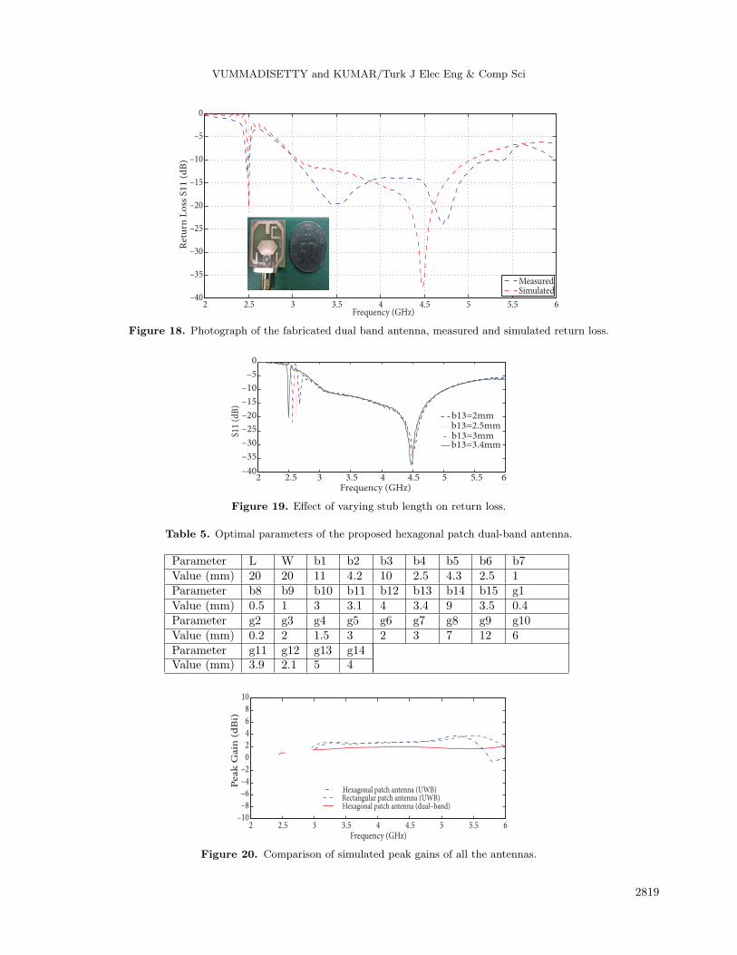
The length of the stub is 16.5 mm, which nearly corresponds to λ/4 at the resonance frequency (2.5 GHz).
A photograph of the fabricated antenna and comparison of measured and simulated return loss are shown in
Figure 18. To illustrate how the length of the stub controls the added resonance, a parametric variation in the
horizontal part of the stub ‘b13’ and its effect on the return loss is shown in Figure 19. As the stub length is
increased, the added resonance shifts towards the lower side.
L
W
b1b8
b2
b7
b1
g1
b2b12 g3
g13
g12
b6
g4
b4g5g2
b5 b5g6
b3
g14
g8
g9
g7
g10
g11
b15
b13
b14
0.5 mm
1.0 mm
b9
x
y
z
Figure 17. Proposed hexagonal patch antenna with L-shape stub for extra resonance.
The simulated peak gains across the operating bands for all the proposed antennas are shown in Figure
20. As can be seen, stable gains across desired bands have been achieved. The simulated peak gains remains
between 1 and 4 dBi in the useful bands.
2818
VUMMADISETTY and KUMAR/Turk J Elec Eng & Comp Sci
2 2.5 3 3.5 4 4.5 5 5.5 6–40
–35
–30
–25
–20
–15
–10
–5
0
Frequency (GHz)
Ret
urn
Lo
ss S
11
(d
B)
MeasuredSimulated
Figure 18. Photograph of the fabricated dual band antenna, measured and simulated return loss.
2.52 3 3.5 4 4.5 5 5.5 6
–35
–40
–30
–25
–20
–15
–10
–5
0
Frequency (GHz)
S11
(dB
)
b13=2mmb13=2.5mmb13=3mmb13=3.4mm
Figure 19. Effect of varying stub length on return loss.
Table 5. Optimal parameters of the proposed hexagonal patch dual-band antenna.
Parameter L W b1 b2 b3 b4 b5 b6 b7Value (mm) 20 20 11 4.2 10 2.5 4.3 2.5 1Parameter b8 b9 b10 b11 b12 b13 b14 b15 g1Value (mm) 0.5 1 3 3.1 4 3.4 9 3.5 0.4Parameter g2 g3 g4 g5 g6 g7 g8 g9 g10Value (mm) 0.2 2 1.5 3 2 3 7 12 6Parameter g11 g12 g13 g14Value (mm) 3.9 2.1 5 4
2 2.5 3 3.5 4 4.5 5 5.5 6–10
–8
–6
–4
–2
0
2
4
6
8
10
Frequency (GHz)
Peak
Gain
(d
Bi)
Hexagonal patch antenna (UWB)Rectangular patch antenna (UWB)Hexagonal patch antenna (dual–band)
Figure 20. Comparison of simulated peak gains of all the antennas.
2819

VUMMADISETTY and KUMAR/Turk J Elec Eng & Comp Sci
8. UWB antenna design
In order to operate the antenna over the entire UWB range (3.1 GHz to 10.6 GHz), the antenna proposed in
Section 2 has been modified and a new design is proposed, given in Figure 21. This proposed antenna consists
of a simple rectangular patch, an L-shaped stub, and an asymmetric staircase shaped ground structure. The
overall dimensions (20 mm × 20 mm) of the antenna are kept the same as in other proposed designs in Section
2. The optimized dimensions of the antenna are given in Table 6. The simulated reflection coefficient (S11)
for the proposed antenna is shown in Figure 22. From the figure, it can be seen that the –10 dB impedance
bandwidth is around 9.2 GHz, starting from 3.1 GHz to 12.3 GHz.
W1
W2
W3
W4
W5
L
W
L1 L2 L3g2
W8
W9
W10
L5
L6
W6
W7
L9
L4
g
L7
L8
g1
Figure 21. Structure of the proposed UWB antenna.
Table 6. Final parameter values of the proposed antenna.
Parameter L W L1 L2 L3 L4 L5 L6 L7Value (mm) 20 20 7.3 2.9 7.4 4.6 2.1 2 3.4Parameter L8 L9 W1 W2 W3 W4 W5 W6 W7Value (mm) 3.9 6 2 3.5 3.9 3 2 8.2 2.5Parameter W8 W9 W10 g g1 g2Value (mm) 4.6 7.9 7 1 1.1 0.7
Figure 23a shows the evolutionary stages of the UWB antenna and its corresponding return loss charac-
teristics are given in Figure 23b. The initial design is a simple rectangular slot containing a rectangular patch.
The bandwidth achieved with this design is 4.5 GHz, from 2.9 GHz to 7.4 GHz. In stage 2 (Figure 23a), by
changing the simple rectangular ground plane profile to an asymmetric slot, bandwidth is extended to 6 GHz
from 3.0 GHz to 9 GHz. Next, in stage 3, a staircase profile is introduced to the ground plane; as a result,
good return loss improvement is achieved at higher frequencies. Finally, by adding an L-shaped stub to the
ground plane nearer to the patch, a good return loss (below –10 dB) in the 5 GHz to 6 GHz band and also
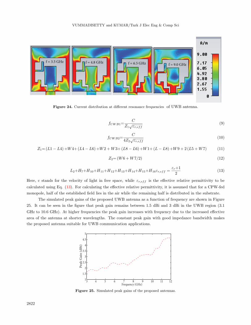
good impedance matching in the entire UWB are achieved. Figure 24 shows the simulated surface current
distribution of the proposed UWB slot antenna. The current distribution is shown at four frequencies. It can
2820

VUMMADISETTY and KUMAR/Turk J Elec Eng & Comp Sci
be seen in the figure that for the proposed UWB antenna, at 3.5 GHz maximum current is distributed on the
slot and much less or zero current is distributed on the patch and on the L-shaped stub. This clearly indicates
that the first resonant frequency is due to the slot perimeter and expression in terms of the slot perimeter ‘Z1’
given in Eq. (9). From Figure 24 it is seen that at 4.8 GHz frequency, the surface current is more on the patch
and slot. This indicates that the resonance at 4.8 GHz frequency is because of the monopole height ‘Z2’. The
expression for the second resonance frequency can be approximated by equating the height of the rectangular
patch to λeff/4 and it is given in Eq. (10). Due to the L-shaped stub and asymmetric staircase shape, the
ground plane and fundamental harmonics of the first two resonant frequencies of the overall bandwidth of the
proposed antenna have been improved. This can be understood by observing the current distribution at 6.5
GHz and 9 GHz in Figure 24.
2 3 4 5 6 7 8 9 10 11 12 13 14–30
–25
–20
–15
–10
–5
0
5
Frequency (GHz)
Ret
urn
Lo
ss (
dB
)
Figure 22. Simulated return loss of the proposed UWB antenna.
stage 1 stage 2
stage 3
proposed antena
Figure 23. a) Evaluation stages of the proposed UWB antenna.
2 3 4 5 6 7 8 9 10 11 12 13 14–45
–40
–35
–30
–25
–20
–15
–10
–5
0
5
Frequency (GHz)
Ret
urn
Lo
ss (
dB
)
stage 2
proposed antenna stage 3
stage 1
Figure 23. b) Simulated return loss against frequency for different stages of the UWB antenna.
2821
VUMMADISETTY and KUMAR/Turk J Elec Eng & Comp Sci
f = 3.5 GHz f = 4.8 GHz f = 6.5 GHz
f = 9.0 GHz
Figure 24. Current distribution at different resonance frequencies of UWB antenna.
fUWB1=C
Z1√εr,eff
(9)
fUWB2=C
4Z2√εr,eff
(10)
Z1=(L1− L4)+W4+ (L4− L6)+W2 +W3+ (L8− L6)+W1+ (L− L8)+W9 + 2 (L5 +W7) (11)
Z2=(W6 +W7/2) (12)
L2+H7+H10+H11+H12+H13+H14+H15+H16εr,eff =εr+1
2(13)
Here, c stands for the velocity of light in free space, while εr,eff is the effective relative permittivity to be
calculated using Eq. (13). For calculating the effective relative permittivity, it is assumed that for a CPW-fed
monopole, half of the established field lies in the air while the remaining half is distributed in the substrate.
The simulated peak gains of the proposed UWB antenna as a function of frequency are shown in Figure
25. It can be seen in the figure that peak gain remains between 1.5 dBi and 3 dBi in the UWB region (3.1
GHz to 10.6 GHz). At higher frequencies the peak gain increases with frequency due to the increased effective
area of the antenna at shorter wavelengths. The constant peak gain with good impedance bandwidth makes
the proposed antenna suitable for UWB communication applications.
3 4 5 6 7 8 9 10 11 121
1.5
2
2.5
3
3.5
4
4.5
5
Frequency (GHz)
Pea
k G
ain
(d
Bi)
Figure 25. Simulated peak gains of the proposed antennas.
2822

VUMMADISETTY and KUMAR/Turk J Elec Eng & Comp Sci
9. Conclusions
Two CPW-fed UWB slot antennas have been designed and experimentally validated. The slot is octagonal
in shape and the radiating elements are rectangular and hexagonal shaped patches. The measured impedance
bandwidth obtained is 2.5 GHz at the center frequency of 4.35 GHz for the rectangular patch antenna and 2.2
GHz at the center frequency of 4.24 GHz for the hexagonal patch antenna. By introducing an additional L-
shaped stub in the ground plane, a dual-band response is obtained in case of the hexagonal patch antenna. The
radiation patterns of both antennas are omnidirectional in the H-plane and bidirectional in the E-plane. The
peak gain is in an acceptable range. These antennas are simple to design and easily integrated with MIC/MMIC
devices. These antennas have potential applications for WLAN and DS-CDMA/MB-OFDM (Group A) UWB
systems.
Acknowledgment
The first author is a doctoral student at Symbiosis International University (Deemed University), Pune, India,
and doing research under the guidance of Dr. Raj Kumar and also acknowledges his support for availing the
Microwave and Millimeter wave Antenna Laboratory Facilities at DIAT (DU).
References
[1] Park JK, An HS, Lee JN. Design of the tree-shaped UWB antenna using fractal concept. Microw Opt Techn Let
2008; 50: 144-150.
[2] Chan KCL, Huang Y. A novel CPS-fed balanced wideband dipole for ultra-wideband applications. In: First
European Conference on Antennas and Propagation; 6–10 November 2006; Nice, France. pp. 1-4.
[3] Lee JN, Park JK, Choi IIH. A compact filter-combined ultra-wide band antenna for UWB applications. Microw
Opt Techn Let 2008; 50: 2839-2845.
[4] Kumar R, Chaubey PN. On the design of CPW-fed pentagonal-cut UWB fractal antenna. Int J Microw Opt Techn
2011; 6: 249-254.
[5] Song HW, Park JK, Yoo JH. A novel ultra-wideband monopole antenna with two symmetrical strips. Microw Opt
Techn Let 2008; 50: 2845-2848.
[6] Kumar R, Malathi P. On the design of CPW-fed diamond shape fractal antenna for UWB applications. Int J
Electron 2011; 98: 1157-1168.
[7] Lee JN, Kim JH, Park JK, Kim JS. Design of dual-band antenna with U-shaped open stub for WLAN/UWB
applications. Microw Opt Techn Let 2009; 51: 284-289.
[8] Lee JN, Park JK. Compact UWB chip antenna design using the coupling concept. Prog Electromagn Res 2009; 90:
341-351.
[9] Yazdanboost KY, Kohno R. Ultra wideband L-loop antenna. In: IEEE International Conference on Ultra-Wideband;
5–8 September 2005; Zurich, Switzerland. pp. 201-205.
[10] Song HW, An HS, Lee JN, Park JK, Kim JS. Design of the tree-shaped UWB antenna using fractal concept. In:
Korea-Japan Microwave Conference; 15–16 November 2007; Okinawa, Japan. pp. 73-76.
[11] Yazandoost KY, Kohno R. UWB antenna for wireless body area network. In: Asia Pacific Microwave Conference;
12–15 December 2006; Yokohoma, Japan. pp. 1647-1652.
[12] Sun XL, Cheung SW, Yuk TI. A compact monopole antenna for WLAN applications. Microw Opt Techn Let 2014;
56: 469-475.
[13] Tsai LC. A triple-band bow-tie-shaped CPW-fed slot antenna for WLAN applications. Prog Electromagn Res C
2014; 47: 167-171.
2823

VUMMADISETTY and KUMAR/Turk J Elec Eng & Comp Sci
[14] Flores RL, Jardon HA, Tirado AM, Acevo RH. Reduced microstrip slot multiband antenna with AU-shaped
resonator for WLAN applications. Microw Opt Techn Let 2012; 54: 2684-2689.
[15] Wu JW, Hsiao HM, Lu JH, Chang SH. Dual broadband design of rectangular slot antenna for 2.4 and 5 GHz
wireless communication. Electron Lett 2004; 40: 1461-1463.
[16] Sadat S, Fardis M, Geran FG, Dadashzadeh GR. A compact microstrip square-ring slot antenna for UWB applica-
tions. Prog Electromagn Res 2007; 67: 173-179.
[17] Azenui NC, Yang HYD. A printed crescent patch antenna for ultrawideband applications. IEEE Antenn Wirel Pr
2007; 6: 113-116.
[18] Dastranj A, Biguesh M. Broadband coplanar waveguide-fed wide-slot antenna. Prog Electromagn Res C 2010; 15:
89-101.
[19] Ma TG, Tseng CH. An ultrawideband coplanar waveguide-fed tapered ring slot antenna. IEEE T Antenn Propag
2006; 54: 1105-1110.
[20] Mitra D, Das D, Bhadra Chaudhuri SR. Bandwidth enhancement of microstrip line and CPW-fed asymmetrical
slot antennas. Prog Electromagn Res Lett 2012; 32: 69-79.
[21] Dawood SJ, Salari MA, Ghoochani OH. Cross-slot antenna with U-shaped tuning stub for ultra-wideband applica-
tions. International Journal of Antennas and Propagation 2008; 2008: 262981.
[22] Kumar R, Naidu PV, Kamble V. Design of asymmetric slot antenna with meandered narrow rectangular slit for
dual band applications. Prog Electromagn Res B 2014; 60: 111-123.
[23] Kushwaha N, Kumar R, Ram Krishna RVS. Design of CPW-fed asymmetric slot UWB antenna for wireless
application. Journal of Electronics (China) 2014; 31: 341-347.
2824