Embed Size (px)
Citation preview

DEPARTMENT OF ELECTRICAL AND ELECTRONIC ENGINEERING
Design of an Isolated DC/DC power converter to
connect a low voltage supercapacitor string to a
DC power system
AUTHOR Angel Guillermo Hidalgo Oñate
SUPERVISOR Dr. Christian Klumpner
DATE September 2016
Project thesis submitted in part fulfilment of the requirements for the degree of Master of
Science Electrical and Electronic Engineering, The University of Nottingham.

1
FINAL REPORT
List of Contents
FINAL REPORT ....................................................................................................................... 1
List of Contents ...................................................................................................................... 1
List of Figures ........................................................................................................................ 4
List of Tables .......................................................................................................................... 9
Acknowledgment ................................................................................................................. 10
Abstract ................................................................................................................................ 11
1. Introduction ................................................................................................................... 12
2. Literature Review.......................................................................................................... 14
2.1. Energy Storage Systems ........................................................................................ 14
2.2. Supercapacitors as energy storage devices ............................................................ 14
2.2.1. Supercapacitor model ..................................................................................... 15
2.2.1. Applications ................................................................................................... 16
2.3. Interface DC-DC converters .................................................................................. 16
2.3.1. Review of the inverter technology ................................................................. 17
2.3.2. Dual Active Bridge (DAB) ............................................................................ 17
2.4. Transformer as galvanic isolator of the DAB ........................................................ 19
2.4.1. Leakage inductance ........................................................................................ 21
2.4.2. Leakage inductance on a DAB ....................................................................... 22

2
2.4.3. Control of leakage inductance ........................................................................ 22
3. Design of the system ..................................................................................................... 24
3.1. Requirements ......................................................................................................... 24
3.2. Design of the string of Supercapacitors ................................................................. 26
3.3. Steady State Operation of Phase Shifted DAB Converter ..................................... 30
3.3.1. Mathematical analysis of Steady State Operation of Phase Shifted DAB
Converter....................................................................................................................... 31
3.4. Design of the high frequency transformer for the prototype ................................. 39
3.4.1. Ideal magnetizing inductance estimation ....................................................... 46
3.4.1. Magnetizing and leakage inductance estimation of the transformer .............. 47
3.4.2. Turn radio of the transformer ......................................................................... 48
3.5. Selection of the Controller ..................................................................................... 49
3.1. Isolation of control signals for gating power devices ............................................ 50
3.2. Selection of the Power Devices ............................................................................. 51
3.3. Snubbers ................................................................................................................ 52
3.4. Control Loop.......................................................................................................... 54
3.4.1. Sensing the supercapacitor voltage ................................................................ 56
3.4.1. Sensing the input current ................................................................................ 57
3.5. Control Algorithm for the prototype ..................................................................... 58
4. Simulation Results and Discussion ............................................................................... 61
4.1. Open Loop Results ................................................................................................ 61

3
4.2. Close Loop Results ................................................................................................ 63
4.2.1. Tracking of Supercapacitor Voltage for different values of ESR .................. 63
4.2.1. Supercapacitor voltage (𝑽𝒐𝒖𝒕 = 𝑽𝟐) when reaches 𝑽𝟐_𝒎𝒂𝒙 or 𝑽𝟐_𝒎𝒊𝒏 .. 63
4.2.2. Supercapacitor Voltage between minimum and maximum values ................ 65
4.2.3. Power Losses .................................................................................................. 66
5. Experimental Results and Discussion ........................................................................... 67
5.1. Open loop experimental results ............................................................................. 71
5.2. Close loop experimental results ............................................................................. 72
6. Conclusion .................................................................................................................... 74
7. References ..................................................................................................................... 75
4
List of Figures
Figure 1. Energy storage system interfaced with MV grid and AC load (based on [6]). ........ 14
Figure 2. (a) Simple model of the supercapacitor including a voltage-dependent shunt current
𝑖𝑃 which models the leakage current (b) Small signal (linear) model for simulation/control
purposes (reprinted from [10]) ................................................................................................. 16
Figure 3. Transformer design flow diagram (Based on [21]) .................................................. 20
Figure 4. Dual Active Bridge converter connecting an ESS ................................................... 24
Figure 5. The supercapacitor module connected to a DC link bus via a charge/discharge
interface (DAB) ....................................................................................................................... 26
Figure 6. Theoretical waveforms when 𝑉1 > 𝑛𝑉2 and positive phase shift (left), negative
phase shift (right) ..................................................................................................................... 30
Figure 7. Typical transformer primary winding current waveform. ........................................ 32
Figure 8. Typical waveform of the output current of the DAB ............................................... 35
Figure 9. Variation of normalized power factor with phase shift ............................................ 37
Figure 10. Leakage inductance required by the DAB for simulation purposes (left) for prototype
(right) ....................................................................................................................................... 39
Figure 11. Transformer primary voltage waveform, illustration the volt-second applied during
the positive portion of the cycle ............................................................................................... 41

5
Figure 12. Non interleaved winding configuration (reprinted from [29]) ............................... 45
Figure 13. Transformer built for the prototype ....................................................................... 46
Figure 14. Model of the transformer neglecting copper resistance and leakage inductance ... 46
Figure 15. Voltage and current applied on the magnetizing inductance .................................. 47
Figure 16. Schematic to measure approximately the magnetizing inductance (left) and the
leakage inductance (right) using the LCR meter HM8018 ...................................................... 48
Figure 17. Primary and secondary sinusoidal voltages applied to the transformer ................. 49
Figure 18. Texas Instrument DSP TMS320F28335 ................................................................ 49
Figure 19. Recommended LED Drive and Application Circuit (based on [31]) ..................... 50
Figure 20. Drain-Source voltage (𝑉𝐷𝑆) of a mosfet (left) HV bridge, and (right) LV bridge 51
Figure 21. Date-Source voltage (𝑉𝐷𝑆) of a mosfet (left) HV bridge, and (right) LV bridge .. 52
Figure 22. Period of ringing frequency (𝑓𝑝) of 𝑉𝐷𝑆 for a MOSFET in (left) HV bridge, and
(right) LV bridge ...................................................................................................................... 53
Figure 23. 𝑉𝐷𝑆 for a MOSFET in (left) HV bridge, and (right) LV bridge after snubber circuit
implementation ........................................................................................................................ 54
Figure 24. Control loop for simulation purposes ..................................................................... 55

6
Figure 25. First stage of the circuit for sensing the supercapacitor voltage ............................ 56
Figure 26. Second stage of the circuit for sensing the supercapacitor voltage ........................ 57
Figure 27. DAB which includes the input current sensor ....................................................... 58
Figure 28. Flow chart of the main program for the DSP ......................................................... 59
Figure 29. Flow chart of the ADC conversion routine ............................................................ 60
Figure 30. DAB results for ideal supercapacitor (constant capacitance, ESR=0, Ip=0A). ...... 61
Figure 31. DAB results for string of supercapacitor (constant capacitance, ESR=150mΩ,
Ip=260uA). ............................................................................................................................... 62
Figure 32. DAB results for string of supercapacitor (constant capacitance, ESR=30mΩ,
Ip=1300uA). ............................................................................................................................. 62
Figure 33. Supercapacitor voltage (Vout = V2) when ESR is 0.5 mΩ (left) and 5 mΩ (right).
.................................................................................................................................................. 63
Figure 34. Supercapacitor voltage (Vout = V2) when reaches V2_max ................................. 64
Figure 35. Control algorithm when V2_max is reached and power reference is changed. ...... 64
Figure 36. Supercapacitor voltage (Vout = V2) when reaches V2_min ................................. 64
Figure 37. Control algorithm when V2_min is reached and power reference is changed. ...... 65

7
Figure 38. Supercapacitor voltage response while power flow reference has positive and
negative values ......................................................................................................................... 65
Figure 39. Comparison of Pin and Pout when the Pref is positive .......................................... 66
Figure 40. Comparison of Pin and Pout when the Pref is negative ......................................... 66
Figure 41. Two H-bridges implemented in breadboard ........................................................... 67
Figure 42. H-bridge for the HV side ........................................................................................ 68
Figure 43. H-bridge for the LV side ........................................................................................ 68
Figure 44. 𝑣𝑎𝑐1 and 𝑣𝑎𝑐2 tested with different power sources and RL load ......................... 69
Figure 45. External inductance of 66.2 µH connected in the LV side ..................................... 69
Figure 46. Input DC current and supercapacitor voltage measurement board. ....................... 70
Figure 47. Whole DAB connected ........................................................................................... 70
Figure 48. 𝑖𝐿 , 𝑣𝑎𝑐1 and 𝑣𝑎𝑐2 waveforms tested with a positive phase shift ........................ 71
Figure 49. 𝑖𝐿 , 𝑣𝑎𝑐1 and 𝑣𝑎𝑐2 waveforms tested with a negative phase shift ....................... 71
Figure 50. 𝑣𝑎𝑐1, 𝑣𝑎𝑐2, 𝑖𝐿 and 𝑖𝑖𝑛 when positive power flow is required (left) transient (right)
steady state ............................................................................................................................... 72

8
Figure 51. 𝑣𝑎𝑐1, 𝑣𝑎𝑐2, 𝑖𝐿 and 𝑖𝑖𝑛 when positive power flow is required and 𝑣𝑎𝑐1 ≈ 𝑛𝑣𝑎𝑐2
.................................................................................................................................................. 72
Figure 52. Supercapacitor voltage linear response (left) increasing (right) decreasing .......... 73
Figure 53. DAB operation when supercapacitor voltage is lower than 𝑉2_𝑚𝑖𝑛 ..................... 73
Figure 54. Duration of input current peak during commutation of HV bridge ........................ 74

9
List of Tables
Table 1. Nomenclature of the DAB used in the report ............................................................ 24
Table 2. System Requirements ................................................................................................ 25
Table 3. Requirements for supercapacitor sizing ..................................................................... 27
Table 4. Data of supercapacitor modules ................................................................................. 29
Table 5. Values of ∆𝐼 ............................................................................................................... 38
Table 6. Core dimensions ........................................................................................................ 42
Table 7. Summary of electrolytic and film capacitors used for HV and LV bridges. ............. 52
Table 8. Summary of RCD snubber circuits for HV and LV bridges. ..................................... 54
Table 9. Voltages measured at each point of the circuit used to sense the voltage of the
supercapacitor string ................................................................................................................ 57

10
Acknowledgment
I would like to express my gratitude to Secretary of Superior Education, Science, Technology
and Innovation of Ecuador (Secretaria de Educación Superior, Ciencia, Tecnología e
Innovación de Ecuador) which has been my sponsor during my studies, without its support
nothing could have been done.
In addition, I would like to thank to the University of Nottingham and to my supervisor
Christian Klumpner who guided to me and contributed actively in order to complete this
project.
Thanks are also due to my family and friends, especially to my mother Aurora who always was
supporting me in spite of the distance. I am very grateful to all.

11
Abstract
This report presents a step by step design procedure for a dual active bridge DAB converter
which is connected to a DC link in the primary side and a supercapacitor module in the
secondary side. The supercapacitors are used in energy storage systems (ESS) as an energy
storage device ESD, in order to save and provide energy according load requirements. The
characteristics of DAB allows the bidirectional power flow and a series inductance connected
to the primary side of the transformer allows the controllability of the system. This inductance
can be an external element or can be the leakage inductance of the transformer. This project
aimed to control the active power flow without an external inductance. Limitation of time and
interference issues have not allowed to complete the close loop design meeting the all
requirements. However, several open and close loop results are presented obtained by
simulation and others obtained using the experimental prototype.

12
1. Introduction
As a consequence of the continuous increase of energy needs of modern life, the development
of high-performance energy storage devices (ESDs) has gained substantial attention [1].
Renewable energy sources going offline and high load demand during short periods of time are
both, problems that an electric power grid normally faces [2] because the power grid must
provide enough energy to the loads at any time.
As a response of sudden changes in load, fast damped oscillations are required as well as
continuous power supplying during transmission or distribution interruptions [3]. Thus, an
Energy Storage System (ESS) can be a suitable solution taking into account maintenance,
flexibility, controllability, reliability and power quality [2]- [3]. Although there are different
technologies for storing energy, supercapacitors deserve a special attention because some of
their characteristics have been enhanced in comparison with batteries and traditional capacitors
[1] such as higher energy density, greater life time and more number of cycles [4].
In a typical ESS, which combines supercapacitors and batteries as ESDs or is made of batteries
only, a low voltage (LV) energy storage cells are interfaced with a medium (MV) or high
voltage (HV) ac grid by means a bidirectional DC/DC converter [5]. Then, several topologies
have been proposed in order to provide the bidirectional power flow [6]. In this project, one of
the approaches is to study the dual active bridge (DAB) as the interface. A DAB converter
includes two H-bridges that are coupled through a high frequency transformer [7]. This
topology is attractive because the transformer provides galvanic isolation between two sides of
the converter and also it allowss large voltage and current transfer ratios [6]. Some
applications, as in aerospace systems [7], require galvanic isolation for sensitive and safety-

13
critical avionic loads in order to reduce supply noise by creating a floating ground on the
secondary side of the DAB [7].
The use of supercapacitors as ESDs is the best option to handle energetic power peaks and
longer lifetime. However, the rating voltage of them are very low, around 2.7 V for a standard
supercapacitor technology, this results in a high voltage boost ratio. In addition, supercapacitors
store energy by exhibiting a wide voltage variation. These facts make the design of the power
converter very challenging, because the operating point is not fixed and normally a large signal
modelling is required [4].
One important element of the converter to control the amount of power flow is the series
external inductance added in the primary [6], [8] or secondary side [7]. However, in terms of
reducing the number of elements taking part of the converter, it can be designed the transformer
with a relatively high and controlled leakage inductance [5], [9]. Depending on the feasibility
of the implementation it can result in reducing of its cost. As it is obvious, there are some
disadvantages if this approach is followed. One of them, it is the fact that the core and copper
losses may increase [5]. Therefore, making an appropriate trade-off during transformer design
is a challenging task which has been addressed in this project building a prototype.
Finally, comments about limitations of the converter design are addressed related to high
frequency transformer, supercapacitor voltage range and semiconductors ratings.
This report starts with the literature review chapter, then the design of the open loop system is
described. After that, the control loop is addressed, then simulation and experimental results
are presented, and finally the conclusion is included.

14
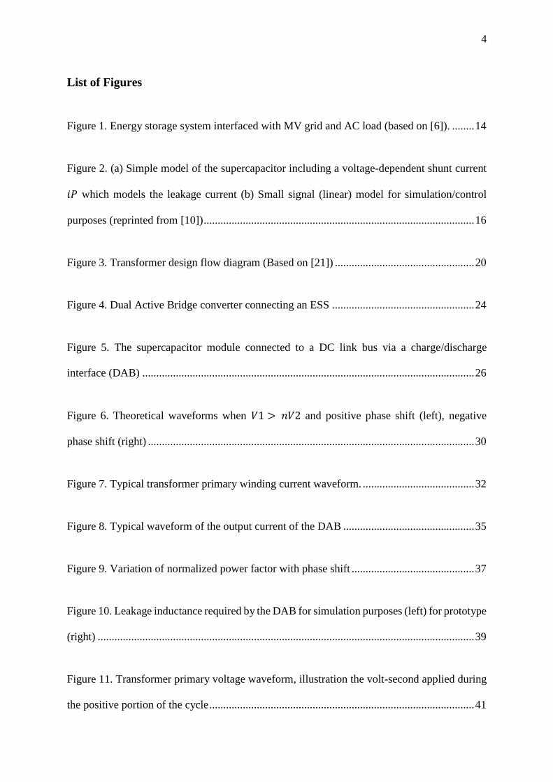
2. Literature Review
2.1. Energy Storage Systems
The necessity of combining future sustainable energy supply with the standard of technical
services and products has motivated to develop and improve energy storage systems (ESS) [1]
in terms of energy density, life time and number of cycles of charging and discharging. The
integration of an ESS enables higher efficiency and cost-effectiveness of the power grid
because problems related to peak demand and the intermittent nature of power sources such as
renewable energies can be solved [1] taking out the needed energy from the ESS.
In general, an ESS combines batteries and supercapacitors as ESDs (refer Figure 1). They
complement each other because while a bank of batteries provides the bulk energy during a
shortage of electric power, a stack of supercapacitors provides the exact peak power required
during transient load conditions [6].
Figure 1. Energy storage system interfaced with MV grid and AC load (based on [6]).
2.2. Supercapacitors as energy storage devices
Supercapacitors are energy storage devices ESDs which increase the energy storage capability
because of a large surface area by means the use of a porous material (frequently made of

15
activated carbon or carbon nano-tubes) [10]. These devices regularly store energy by means of
an electrolyte solution between two solid conductors [11]. The difference with ordinary
electrostatic and electrolytic capacitors is that supercapacitors exhibit an ionically conducting
solution between the electrodes [3], [12]. Supercapacitors are compact in size, easy to install,
and can operate effectively in different environments such as hot, cold, and moist ones. They
can be charged substantially faster than conventional batteries [11]. Characteristics as low
energy density and capability of huge number of cycling periods (over 100 000 [11]) are
reasons why fast cycling high power applications are recommended for supercapacitors [3],
[11].
Commercially, supercapacitors are available at low operation voltage of between 2.5 and 2.7
V. Nevertheless, most high power applications require considerably higher voltages. Therefore,
multiple supercapacitors are interconnected in series in order to increase this feature [13], [12]
to lower the converter current.
2.2.1. Supercapacitor model
Figure 2 (a) shows an approximate electrical model of a supercapacitor that consist of an
equivalent series resistance (ESR) 𝑅𝐶0, an ideal linear capacitor 𝐶0 in parallel with another
voltage-depended capacitor 𝐶(𝑈𝐶) and a shunt resistance 𝑅𝑃 (which models the leakage current
of the supercapacitors). Also, Figure 2 (b) depicts the small signal (linear) model used for
simulation and control [10]. Either ESR and capacitance are frequency-depending. However,
the models presented assume that ESR and capacitance are frequency-independent parameters
[10]. The simplest way to model a supercapacitor is a ESR in series with a constant
capacitance.

16
Figure 2. (a) Simple model of the supercapacitor including a voltage-dependent shunt current 𝑖𝑃 which models
the leakage current (b) Small signal (linear) model for simulation/control purposes (reprinted from [10])
2.2.1. Applications
Supercapacitors integrated with an interface DC-DC converter are typically used in
applications in order to smooth down strong variations of the load or input power [12]- [10].
For instance, in renewable energy source systems (wind, PV, and marine current) are useful
because variations of the input power should not be transferred to the grid [12]. In addition,
for UPS systems, the load must not be affected by the supply interruption. Another common
application, where energy storage systems must compensate the power flow fluctuations, takes
place in controlled electric drives where two scenarions can occur. Firstly, motor load
variations (e.g. braking and peak power such as in elevators) and secondly, interruption of
power supplying, as worst case when ride-through capability should apply [12]- [10].
2.3. Interface DC-DC converters
In order to charge and discharge the supercapacitors, a DC-DC converter is required as an
interface to connect the DC bus with the energy storage system [10] which allows bidirectional
power flow between input and output [14]. Three control objectives are required to the
interface, firstly, monitoring of the supercapacitor DC voltage to keep it within a valid range
17
[7]. Secondly, smoothing the drive input power, regardless any variation of the drive load.
Finally, monitoring the supercapacitor state of the charge, including control of the
supercapacitor current [10].
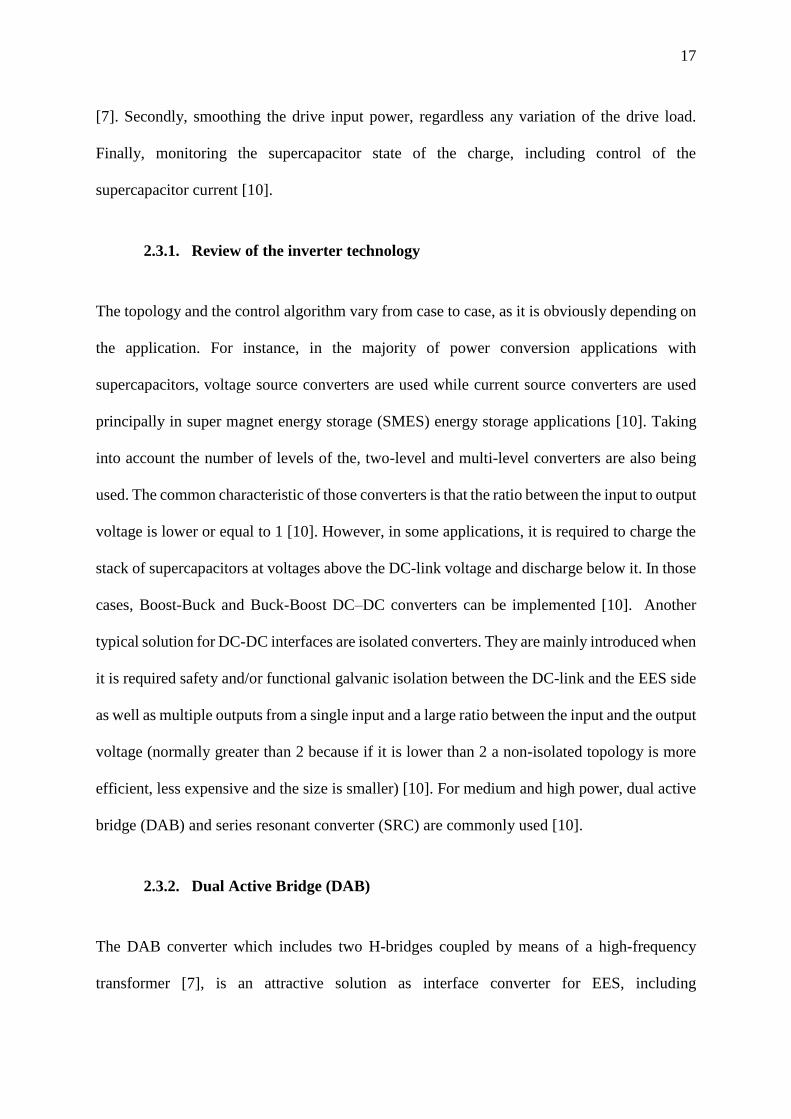
2.3.1. Review of the inverter technology
The topology and the control algorithm vary from case to case, as it is obviously depending on
the application. For instance, in the majority of power conversion applications with
supercapacitors, voltage source converters are used while current source converters are used
principally in super magnet energy storage (SMES) energy storage applications [10]. Taking
into account the number of levels of the, two-level and multi-level converters are also being
used. The common characteristic of those converters is that the ratio between the input to output
voltage is lower or equal to 1 [10]. However, in some applications, it is required to charge the
stack of supercapacitors at voltages above the DC-link voltage and discharge below it. In those
cases, Boost-Buck and Buck-Boost DC–DC converters can be implemented [10]. Another
typical solution for DC-DC interfaces are isolated converters. They are mainly introduced when
it is required safety and/or functional galvanic isolation between the DC-link and the EES side
as well as multiple outputs from a single input and a large ratio between the input and the output
voltage (normally greater than 2 because if it is lower than 2 a non-isolated topology is more
efficient, less expensive and the size is smaller) [10]. For medium and high power, dual active
bridge (DAB) and series resonant converter (SRC) are commonly used [10].
2.3.2. Dual Active Bridge (DAB)
The DAB converter which includes two H-bridges coupled by means of a high-frequency
transformer [7], is an attractive solution as interface converter for EES, including

18
supercapacitors as ESD (refer Figure 4). It is able to achieve bidirectional power flow and
galvanic isolation between energy storage and load side [15]. This topology is commonly used
for its low device count and component stresses because of low VA ratings of the
semiconductor switches. Moreover, DAB includes small filter components, low switching
losses, zero-voltage switching (ZVS) within certain limits [6], high power density, high
efficiency and feasibility of buck-boost operation [7]. Bidirectional power transfer is allowed
because each inverter has two-quadrant capability [6]. The reactive network in a DAB includes
an inductor 𝐿𝑒𝑥𝑡 which can be an external one [7] or just the leakage inductance of the
transformer, if sufficiently large [5], [9].
Furthermore, the waveforms of the transformer currents in the primary and secondary side are
highly depending on the terminal voltage of the supercapacitors. For this reason, high
transformer RMS currents are obtained when the supercapacitor voltage is minimum [6]. In
addition, the control algorithms used to generate the gate signals for the power devices
(MOSFETs or IGBTs) [6] and meet the requirements getting high performance of the converter
can increase the complexity in terms of implementation.
Several papers have been published related to applications, where a DAB has been interfaced
with a ESS. In [15], it has been proposed a composite energy storage system (CESS) for
microgrid application to compensate the intermittent nature of renewable energy sources, using
PV as example, and the continuous variations of the load. The CESS has been implemented
based on DAB modules whose terminals are connected in series or parallel depending on need
and feasibility. The modularity of the system allows sharing the power between different
batteries and supercapacitor with enough flexibility. In [16], a smart user network (SUN) is
studied, where SUN includes several kinds of micro-generation and small storage systems.
Moreover, in [17], mathematical analysis of DAB is presented. In order to avoid circulation of

19
an excessive reactive current, the value of phase shift is limited to 0.275 to have a power factor
in the primary side of the converter equal to 0.8 or higher.
On the other hand, there are some topologies for resonant DC–DC converters. Most of them
are related to unidirectional power plow. Bidirectional power flow is also possible but they are
less popular because they might have higher converter complexity and additional HF
components are necessary [6].
2.4. Transformer as galvanic isolator of the DAB
The transformer is indispensable for voltage matching and/or galvanic isolation between the
utility grid and the energy storage device [18]. Designing a power and high-frequency
transformer is based on trade-off of different facts such as core material, turn ratio, frequency
of operation, windings, efficiency, output power, weight, cost and physical dimensions [19],
[20]. High-frequency operation presents design problems because of increased effects of core
losses, leakage inductance, and winding capacitance [19]
In order to have a suitable control of the currents in the DAB, it is required a leakage inductance
(𝐿) with a desired value. If a separate inductor in series with the transformer is added, it
increases overall size, cost and losses of the magnetic device, as long as if the leakage
inductance of the transformer is intelligently modified (to meet the requirement), it is possible
to have a better solution which optimizes the overall cost because of less hardware required,
and better controllability of the power flow [5]. Precisely the second solution is more
challenging and it will be reviewed as part of this project. Thus, Figure 3 shows a flow diagram
which summarizes one procedure to design a high frequency transformer.

20
START
Specify:1. Wire effective resistivity (r)2. Total rms winding current, referred to the primary (I_tot)3. Desired turn ratio (n)4. Applied primary volt-seconds ( l1)5. Allowed total power dissipation (P_tot)6. Winding fill factor (Ku)7. Core loss exponent (b)8. Core loss coefficient (Kfe)
Calculate the threshold of Kgfe
Select a core and a geometry which meet Kgfe threshold
Calculate the peak AC flux density (DB)
DB + margin < Bsat
Calculate the number of turns for the primary side (n1)
Calculate the number of turns for the secondary side (n2)
Evaluate fraction of window area allocated to each winding
Evaluate wire sizes
Evaluate other phenomema that can appear such as skin effect and copper
losses due to the proximity effect
Depending on the requeriments, estimate parameters of the transformer such as
magnetizing inductance, leakage inductance, peak ac magnetizing current,
winding resistences or others.
Determine the winding geometry
Define core dimensions:1. Core cross-section area (Ac)2. Core Window Area (WA)3. Mean length per turn (MLT)4. Magnetic path length (lm)5. Saturation flux density (Bsat)
Build the transformer
END
YES
NO
Parameter estimated @ Parameter requerired
YES
NO
Figure 3. Transformer design flow diagram (Based on [21])

21
2.4.1. Leakage inductance
Transformer leakage inductance (𝐿) is an inductive component which is distributed along the
windings of a transformer and results from the imperfect magnetic linking of primary winding
to secondary [19]. This parameter affects negatively the performance of the transformer [22]
because losses increase and higher magnetizing current is required. It is related to the energy
of the magnetic field linked to the windings. This energy is obtained by means equation (1),
where μ is the permeability of a space where the energy is calculated, V is the volume of the
space, H is the magnetic field intensity and I is the current flowing through the windings. [23]
12
𝐿𝐼2 =12
∫ 𝜇𝐻2𝑑𝑉𝑉𝑤
(1)
From (1), it can be noticed that the leakage inductance depends on the several parameters such
as core geometry. Then, in order to estimate the value of 𝐿, a general expression for the leakage
inductance of a split winding arrangement is shown in (2). The expression takes into account
the insulation between adjacent conductors in the same layer [24].
𝐿 ≈𝜇𝑜𝑛1
2𝑀𝐿𝑇
𝑝2ℎ𝑤(𝑏𝐶𝑢
3+ 𝑏𝑖)
(2)
Where 𝑝 is the number of winding partitions, n1 is the primary winding turns, 𝑀𝐿𝑇 is the
mean turn per length, ℎ𝑤 is the core window height, 𝑏𝐶𝑢 is the total width of the copper in the
winding window and 𝑏𝑖 is the interwinding insulation thickness.

22
2.4.2. Leakage inductance on a DAB
Leakage inductance cause voltage spikes during commutation, which could be destructive to
power devices such as MOSFETs. Voltage spikes always appear on the rising edge of the
transistor voltage waveform. In addition, leakage inductance can be observed by the leading
edge slope of the trapezoidal current waveform [19]. Since leakage inductance and winding
resistance of a high frequency transformer are dependent each other, typically, any rise in
leakage inductance implies an increase of the winding resistance and transformer efficiency is
affected [5]. Furthermore, while a small value of the inductance causes instability in the control
at low current, a large inductance limits the power transfer capability [5]. Therefore, for
transformer designing purposes, there must be a compromise between leakage inductance and
the winding losses [5].
2.4.3. Control of leakage inductance
In order to control the leakage inductance, the leakage flux must be modified [19]. Core
material, its geometry, windings are some parameters which cause a variation of leakage flux
winding design, its arrangement and evaluation [5]. In Eq. 2, it can be noticed that the leakage
inductance can be modified by varying the field intensity (𝐻) in the winding space, the volume
of the windings (𝑉𝑤) and/or permeability of the winding space (𝜇) [23].
Some attempts have been tried, in [23] for instance, a leakage layer, which has high
permeability, was inserted between the winding layers. This fact increases the leakage field
locally and then it increases the leakage inductance. Although, the simulation results were
acceptable, the experimental ones failed because of isolation breakdown in prototype. Another
attempt was performed in [5]. Different asymmetric winding arrangements were evaluated and

23
a flux diverter caps made of a relatively small amount of ferrite material was used. The aim
was to get the desired value of inductance whilst maintaining the losses in the windings at
acceptable levels. In this case, the leakage inductance has been increased without affecting the
value of the winding resistance.
24
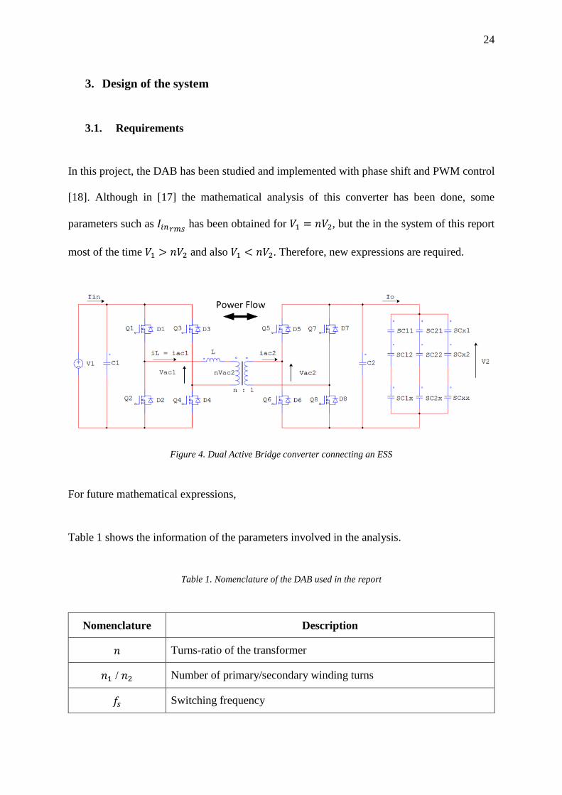
3. Design of the system
3.1. Requirements
In this project, the DAB has been studied and implemented with phase shift and PWM control
[18]. Although in [17] the mathematical analysis of this converter has been done, some
parameters such as 𝐼𝑖𝑛𝑟𝑚𝑠 has been obtained for 𝑉1 = 𝑛𝑉2, but the in the system of this report
most of the time 𝑉1 > 𝑛𝑉2 and also 𝑉1 < 𝑛𝑉2. Therefore, new expressions are required.
Figure 4. Dual Active Bridge converter connecting an ESS
For future mathematical expressions,
Table 1 shows the information of the parameters involved in the analysis.
Table 1. Nomenclature of the DAB used in the report
Nomenclature Description
𝑛 Turns-ratio of the transformer
𝑛1 / 𝑛2 Number of primary/secondary winding turns
𝑓𝑠 Switching frequency

25
𝑇𝑠 = 1/𝑓𝑠 Half switching period (for the convenience of analysis)
𝑉1 DC input voltage of the secondary bridge (DC link)
𝑉2 DC output voltage of the secondary bridge (Supercapacitors)
𝑛𝑉2 DC output voltage of the secondary bridge referred to the primary side
𝑣𝐴𝐶1 Transformer primary voltage
𝑣𝐴𝐶2 Transformer secondary voltage
𝑇𝜑 = 𝑑𝑇𝑠
2
Phase-shift between the two bridges
𝐿 Leakage inductance of the transformer
𝐿𝑚 Magnetizing inductance of the transformer
𝐿𝑒𝑥𝑡 Probable eternal inductance to be added
𝑖𝐿 = 𝑖𝐴𝐶1 Current through the leakage inductance
𝑖𝐴𝐶2 Current in the secondary side of the transformer
In order to study and analyze the DAB as interface to control the power flow between the DC-
link and the string of supercapacitors, this project has been split in two parts, simulation and
implementation. Therefore, different set of specs/requirements have been used and these are
shown in Table 2.
Table 2. System Requirements
Requirements Simulation Experimental
DC-link voltage 400 V 60 V
Maximum voltage of the supercapacitors 40 V 12 V
Rated power ± 10 kW ± 100 W
Frequency range 2 to 5 kHz 10 and 20 kHz
26
Taking into account the requirements given in Table 2, it is necessary to derive other parameters
for designing the system.
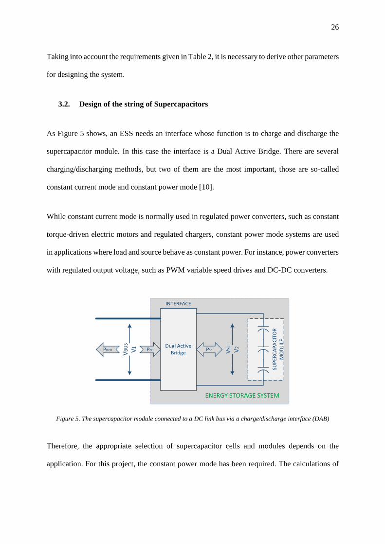
3.2. Design of the string of Supercapacitors
As Figure 5 shows, an ESS needs an interface whose function is to charge and discharge the
supercapacitor module. In this case the interface is a Dual Active Bridge. There are several
charging/discharging methods, but two of them are the most important, those are so-called
constant current mode and constant power mode [10].
While constant current mode is normally used in regulated power converters, such as constant
torque-driven electric motors and regulated chargers, constant power mode systems are used
in applications where load and source behave as constant power. For instance, power converters
with regulated output voltage, such as PWM variable speed drives and DC-DC converters.
Figure 5. The supercapacitor module connected to a DC link bus via a charge/discharge interface (DAB)
Therefore, the appropriate selection of supercapacitor cells and modules depends on the
application. For this project, the constant power mode has been required. The calculations of

27
supercapacitor sizing have been based on the second method for constant power mode provided
in an application note by Tecate Group [25].
In addition, some assumptions have been taken. For instance, a 1:2 𝑉𝑚𝑖𝑛/𝑉𝑚𝑎𝑥 supercapacitor
voltage variation as well as equal charging/discharging times have been chosen. Table 3
summarizes the complete information used for the supercapacitor sizing.
Table 3. Requirements for supercapacitor sizing
Requirements Simulation Experimental
DC-link voltage 400 V 60 V
Maximum voltage of the supercapacitors 40 V 12 V
Maximum power ± 10 kW ± 100 W
Charge/Discharge time 0.3 s 3 s
Supercapacitor voltage variation 50 % 50 %
Minimum voltage of the supercapacitors 20 V 6 V
This method used is based on the energy needed. In [25] it is mentioned that this method works
well for low power application where the losses because of ESR are minimal. Then, the
calculations that are shown are related to simulation purposes. For the prototype
implementation, the results are presented in Table 4.
𝐸𝑛𝑒𝑟𝑔𝑦 𝑛𝑒𝑒𝑑𝑒𝑑 = 𝑃𝑜𝑤𝑒𝑟 ∗ ∆𝑡 [𝐽] (3)
𝐸𝑛𝑒𝑟𝑔𝑦 𝑛𝑒𝑒𝑑𝑒𝑑 = 10000 ∗ 0.3 [𝐽] (4)
𝐸𝑛𝑒𝑟𝑔𝑦 𝑛𝑒𝑒𝑑𝑒𝑑 = 3000 [𝐽] (5)
On the other hand, taking into account the energy which is stored in a capacitor:

28
𝐸𝑛𝑒𝑟𝑔𝑦 𝑠𝑡𝑜𝑟𝑒𝑑 = 0.5 ∗ 𝐶𝑇 ∗ (𝑉𝑚𝑎𝑥2 − 𝑉𝑚𝑖𝑛
2 ) (6)
Making 𝐸𝑛𝑒𝑟𝑔𝑦 𝑛𝑒𝑒𝑑𝑒𝑑 = 𝐸𝑛𝑒𝑟𝑔𝑦 𝑠𝑡𝑜𝑟𝑒𝑑 = 𝐸 :
𝐶𝑇 =2 ∗ 𝐸
(𝑉𝑚𝑎𝑥2 − 𝑉𝑚𝑖𝑛
2 )
(7)
𝐶𝑇 =2 ∗ 3000
(402 − 202)
(8)
𝐶𝑇 = 5 F (9)
However, it is known that a supercapacitor normally has low rated terminal voltage [10]. This
limitation makes that the performance of supercapacitors is degraded significantly if the
voltage is tried to increase. For these reason, it is necessary to connect several supercapacitors
in series in order to achieve the voltage required by the application. Furthermore, if the
capacitance is not enough it is required that supercapacitors are connected in parallel as well.
Then, taking into account 2.7 V as a rated voltage of the supercapacitor, the number of elements
that have to be connected in series is defined as follows:
𝑆𝑒𝑟𝑖𝑒𝑠 =𝑉𝑚𝑎𝑥
𝑉𝑟𝑎𝑡𝑒𝑑
(10)
𝑆𝑒𝑟𝑖𝑒𝑠 =40 𝑉
2.7 𝑉= 14.8
(11)
𝑆𝑒𝑟𝑖𝑒𝑠 = 15 (12)
Now, applying the principle of adding capacitors in series, it is possible to figure out the
minimum value of individual capacitance required for the application. Since 𝐶1 = 𝐶2 = ⋯ =
𝐶15 = 𝐶, the result is:
1
𝐶𝑇=
15
𝐶
(13)

29
𝐶 = 15 ∗ 𝐶𝑇 = 15 ∗ 5 = 75 𝐹 (14)
At this point is important to analyze mainly two facts: a) Commercial availability, and b)
Equivalent Series Resistance (ESR). In the first case, PowerStore supplier offers a range of
different values of capacitance, the nearest one is 100 F @ 2.7 V [26] and depending on the
frequency of operation the ESR changes from 10 mΩ at 1 kHz to 12 mΩ at 100 kHz. Then for
this work the value chosen is 10 mΩ. Thus, the total ESR is:
𝐸𝑆𝑅𝑇 = 15 ∗ 10 𝑚𝛺 (15)
𝐸𝑆𝑅𝑇 = 150 𝑚𝛺 (16)
This value of 𝐸𝑆𝑅𝑇 is acceptable depending on the amount of current flowing through the
circuit, which will be considered later on. For the prototype the same procedure has been
followed. Table 4 depicts the summary of the results for the both systems.
Table 4. Data of supercapacitor modules
Parameters Simulation Experimental
Minimum total capacitance 5 F 5.56 F
Number of elements in series 15 5
Parallel arrangement 1 1
Nominal working voltage 2.7 V 2.7 V
Individual capacitance 100 F 100 F
Real total capacitance 6.6 F 20 F
Total ESR 150 mΩ 50 mΩ
Real maximum voltage per supercapacitor 2.6 V 2.4 V
Nominal leakage current after 72 hours at
20ºC
260 uA 260 uA

30
3.3. Steady State Operation of Phase Shifted DAB Converter
In Figure 6, it can be seen the simplified theoretical waveforms of the DAB when 𝑉1 > 𝑛𝑉2
and Phase Shift Modulation [6], which match with the proposed system, either positive phase
shift (power flow from left to right side – string of supercapacitors charge) and negative phase
shift (power flow from right to left side – string of supercapacitors discharge). The waveforms
of the current look slightly different in [7], this is because the assumption there, is 𝑉1 < 𝑛𝑉2.
The DAB produces square voltages 𝑣𝐴𝐶1 and 𝑣𝐴𝐶2.
Figure 6. Theoretical waveforms when 𝑉1 > 𝑛𝑉2 and positive phase shift (left), negative phase shift (right)
In [17], it can be seen that the power transfer 𝑃𝐷 can be controlled by adjusting the phase shift
(d) between 𝑣𝐴𝐶1 and 𝑣𝐴𝐶2.
𝑃𝐷 =𝑛𝑉1𝑉2𝑇𝑠𝑑(1 − 𝑑)
2𝐿
(17)
For the system proposed, 𝑇𝑠 is the period of the switching signal, and 𝐿 is the whole transformer
leakage inductance [18]. If 𝑉1 < 𝑛𝑉2, 𝑃𝐷 must change the directions, it means that the phase

31
shift (𝑑) should be higher than 𝑇𝑠/2. In addition, the other parameters that affect power transfer
is the switching frequency (𝑓𝑠) and the inductance 𝐿.
From the previous equation, it can be derived that the maximum amount of transferring power
occurs when 𝑑 = 0.5 [6]. Then:
𝑃𝐷𝑚𝑎𝑥 =𝑛𝑉1𝑉2𝑇𝑠
8𝐿
(18)
However, it is not recommended to set up the system at this operational point because the
amount of reactive power becomes the same as the active power [17]. Then, the power factor
is low. It means that high reactive currents flow through the converter. This fact increases the
power losses as well as the size of wires and sizing of power devices.
3.3.1. Mathematical analysis of Steady State Operation of Phase Shifted DAB
Converter
As it has previously been stated that the aim of this project is to design and practically
implement a phase shifted DAB converter. Therefore, steady state analyses of the converter.
Then, for steady state analyses purposes, several assumptions have been made:
All losses are neglected because power devices like MOSFETs and diodes are ideal (no
recovery, no voltage drop and switching at zero time)
Phase shift control only.
All low voltage (LV) quantities are referred to the high voltage (HV) side.
The magnetizing inductance and parasitic capacitance in the transformer is neglected
Constant supply voltages 𝑉1 and 𝑉2 are considered.

32
It is important to point out that mathematical analysis has been done because based on the
equations that describes the DAB, the value of the leakage inductance of the transformer (𝐿)
required for the converter operation has been obtained. Some equations have been taken from
past papers (𝑃𝐷 and 𝑝𝑓), but others have been derived from scratch (∆𝑖1, ∆𝑖2, ∆𝐼, 𝑖𝑀𝐴𝑋, 𝐼𝑖𝑛𝑟𝑚𝑠
and 𝐼𝑂) for two main reasons: firstly, the converter topology is not exactly the same as the
topology presented in this report. For instance, most of the paper present equations when 𝑉1 =
𝑛𝑉2 [17], or when the series inductance is modeled in the secondary [7] or when input and output
filters are included [6] or when the transformer turn ratio is 1/n [27]. Secondly, the
nomenclature also is different. For instance, while in [6], phase shift is considered as angle, in
[17], the phase shift is a fraction of the half of the switching period (𝑇𝑠/2).
Figure 6 depicts the complete waveforms for phase shift control operation of the DAB.
However, for the steady state analysis, the leakage inductor current is mainly used (refer to
Figure 7). The case which is analyzed is when the power flow is towards the string of
supercapacitors and 𝑉1 > 𝑛𝑉2.
Figure 7. Typical transformer primary winding current waveform.
The waveform can be mathematically defined expressed as follows:
𝑖𝐿(𝑡) = 𝑖𝐿(0) + 𝑉1+𝑛𝑉2
𝐿𝑡 𝑤ℎ𝑒𝑛 0 < 𝑡 < 𝑇𝜑 – MODE I (19)

33
𝑖𝐿(𝑡) = 𝑖𝐿(𝑇𝜑) + 𝑉1−𝑛𝑉2
𝐿(𝑡 − 𝑇𝜑) 𝑤ℎ𝑒𝑛 𝑇𝜑 < 𝑡 < 𝑇𝑠/2 – MODE II (20)
Looking into the Figure 7 it can be seen that if 𝑡 = 𝑇𝜑 then 𝑖𝐿_𝑀𝑂𝐷𝐸 𝐼 = 𝑖𝐿_𝑀𝑂𝐷𝐸 𝐼𝐼
𝑖𝐿(0) +(𝑉1 + 𝑛𝑉2)𝑇𝜑
𝐿= 𝑖𝐿 (𝑇𝜑) +
(𝑉1 − 𝑛𝑉2)
𝐿(𝑇𝜑 − 𝑇𝜑)
(21)
Then:
∆𝑖1 = −𝑖𝐿(0) + 𝑖𝐿 (𝑇𝜑) =𝑉1 + 𝑛𝑉2
𝐿𝑇𝜑
(22)
Evaluating the 𝑖𝐿(0), and 𝑖𝐿 (𝑇𝜑), the result is:
𝑖𝐿(0) = (𝑛𝑉2 − 𝑉1
2𝐿)
𝑇𝑠
2−
𝑛𝑉2
𝐿𝑇𝜑
(23)
𝑖𝐿(𝑇𝜑) = (𝑛𝑉2 − 𝑉1
2𝐿)
𝑇𝑠
2+
𝑉1
𝐿𝑇𝜑
(24)
Then:
𝑖𝐿 (𝑇𝑠
2) = 𝑖𝐿(𝑇𝜑) +
𝑉1 − 𝑛𝑉2
𝐿(
𝑇𝑠
2− 𝑇𝜑)
(25)
∆𝑖𝐿2= 𝑖𝐿 (
𝑇𝑠
2) − 𝑖𝐿(𝑇𝜑) =
𝑉1 − 𝑛𝑉2
𝐿(
𝑇𝑠
2− 𝑇𝜑)
(26)
∆𝑖𝐿2=
𝑉1 − 𝑛𝑉2
𝐿(
𝑇𝑠
2− 𝑇𝜑)
(27)
From Figure 6, it is also possible to see that maximum value of 𝑖𝐿 varies depending on the 𝑉1
and 𝑛𝑉2. Therefore:
𝑖𝑀𝐴𝑋 = 𝑖(
𝑇𝑆2
)= (
𝑉1 − 𝑛𝑉2
2𝐿)
𝑇𝑠
2+
𝑛𝑉2
𝐿𝑇𝜑 𝑖𝑓 𝑉1 > 𝑛𝑉2
(28)
𝑖𝑀𝐴𝑋 = 𝑖(𝑇𝜑) = (𝑛𝑉2 − 𝑉1
2𝐿)
𝑇𝑠
2+
𝑉1
𝐿𝑇𝜑 𝑖𝑓 𝑉1 < 𝑛𝑉2
(29)

34
As was shown before 𝑇𝜑 = 𝑑𝑇𝑠
2 , then:
𝑖𝑀𝐴𝑋 =𝑉1 − (1 − 2𝑑)𝑛𝑉2
4𝐿𝑓𝑠 𝑖𝑓 𝑉1 > 𝑛𝑉2
(30)
In addition, the expression in order to obtain the input rms current has been derived applying
the general definition.
𝐼𝑖𝑛𝑟𝑚𝑠
2 =1
𝑇𝑠
2
[∫ (𝑖𝐿(0) +𝑉1 + 𝑛𝑉2
𝐿𝑡)
2
𝑑𝑡 + ∫ (𝑛𝑖𝐿(𝑇𝜑) +𝑉1 − 𝑛𝑉2
𝐿(𝑡 − 𝑇𝜑))
2
𝑑𝑡𝑇𝑠
2⁄
𝑇𝜑
𝑇𝜑
0
] (31)
After a long and careful mathematical process to evaluate the expression, the result is:
𝐼𝑖𝑛𝑟𝑚𝑠
2 =2
𝑇𝑆
[(10
3
𝑛𝑉1𝑉2
𝐿2− 4
𝑉12
𝐿2) 𝑇𝜑
3 + 𝑇𝜑2𝑇𝑠 [
𝑉12
𝐿2−
3
2
𝑛𝑉1𝑉2
𝐿2+
𝑛2𝑉2
𝐿2] +
𝑇𝑆3
96(
𝑛2𝑉22
𝐿2−
2𝑛𝑉1𝑉2
𝐿2+
𝑉12
𝐿2)]
(32)
Considering that 𝑇𝜑 = 𝑑 𝑇𝑆
2 , the expression is:
𝐼𝑖𝑛𝑟𝑚𝑠
2 =𝑇𝑆
2
2𝐿2(𝑛𝑉1𝑉2 (
5
3𝑑3 −
3
2𝑑2 −
1
12) − 𝑉1
2 (2𝑑3 − 𝑑2 −1
24) + 𝑛2𝑉2
2 (𝑑2 +1
24))
(33)
𝐼𝑖𝑛𝑟𝑚𝑠= √
𝑇𝑆2
2𝐿2(𝑛𝑉1𝑉2 (
5
3𝑑3 −
3
2𝑑2 −
1
12) − 𝑉1
2 (2𝑑3 − 𝑑2 −1
24) + 𝑛2𝑉2
2 (𝑑2 +1
24))
(34)
For the specific case where 𝑛𝑉2 = 𝑉1, the expression becomes:
𝐼𝑖𝑛𝑟𝑚𝑠
2 =𝑇𝑆
2𝑉12𝑑2
4𝐿2(
3 − 2𝑑
6)
(35)
𝐼𝑖𝑛𝑟𝑚𝑠= √
𝑇𝑆2𝑉1
2𝑑2
4𝐿2(
3 − 2𝑑
6)
(36)
In addition, Figure 8 shows the typical waveform of the output current of the DAB, the
expression for its average value has been also derived.

35
Figure 8. Typical waveform of the output current of the DAB
Applying the definition of the average value, next expression must be evaluated:
𝐼0 =1
𝑇𝑆
2
[− ∫ (𝑛𝑖𝐿(0) + 𝑛𝑉1 + 𝑛𝑉2
𝐿𝑡) 𝑑𝑡 + ∫ (𝑛𝑖𝐿(𝑇𝜑)
𝑇𝑠2⁄
𝑇𝜑
+ 𝑛𝑉1 − 𝑛𝑉2
𝐿(𝑡 − 𝑇𝜑))
𝑇𝜑
0
𝑑𝑡] (37)
As a result, it has been obtained:
𝐼0 =2𝑛𝑉1𝑇𝜑
𝐿𝑇𝑆[𝑇𝑆
2− 𝑇𝜑]
(38)
When 𝑇𝜑 = 𝑑𝑇𝑠
2
𝐼0 =𝑛𝑉1𝑇𝑠
2𝐿𝑑(1 − 𝑑)
(39)
On the other hand, from [17] the value of ∆𝐼 (refer to Figure 7) has been obtained:
∆𝐼 = ∆𝑖𝐿1+ ∆𝑖𝐿2
(40)
∆𝐼 = (𝑉1 + 𝑛𝑉2)𝑑𝑇𝑆
2𝐿+ (𝑉1 − 𝑛𝑉2)
(1 − 𝑑)𝑇𝑆
2𝐿
(41)
∆𝐼 =𝑇𝑠
2𝐿(𝑉1 + 𝑛𝑉2(2𝑑 − 1))
(42)
Expressions of ∆𝐼 and for 𝑃𝐷 incudes 𝐿, then getting 𝐿 from ∆𝐼 equation:

36
𝐿 =𝑇𝑆
2∆𝐼(𝑉1 + 𝑛𝑉2(2𝑑 − 1))
(43)
The leakage inductance (𝐿) can be also derived from expression of 𝑃𝐷 (17):
𝐿 =𝑛𝑉1𝑉2𝑇𝑆𝑑(1 − 𝑑)
2𝑃𝐷
(44)
Then, (43) and (44) equations of 𝐿 can be matched.
𝑇𝑆
2∆𝐼(𝑉1 + 𝑛𝑉2(2𝑑 − 1)) =
𝑛𝑉1𝑉2𝑇𝑆𝑑(1 − 𝑑)
2𝑃𝐷
(45)
∆𝐼 = 𝑃𝐷
(𝑉1 + 𝑛𝑉2(2𝑑 − 1))
𝑛𝑉1𝑉2𝑑(1 − 𝑑)
(46)
As it can be seen the variation of current depends on the active power, voltage in the DC bus,
voltage in the supercapacitor side and the phase shift between waveforms.
In [17], it is also obtained the expression for the power factor in the primary side of the DAB,
which only depends on the phase shift.
𝑝𝑓 = (1 − 𝑑)√3
3 − 𝑑
(47)
This is an important parameter to take into account, actually Figure 9 depicts the variation of
normalized power factor with phase shift.
In order to make best use of the transformer capacity, the Dual Active Bridge should be
designed to operate with low values of phase shift [17]. Therefore, the power factor is high as
well as the ratio of active power to apparent power. If 𝑑𝑚𝑎𝑥 = 0.15, the power factor will be
0.9 or greater as well as if 𝑑𝑚𝑎𝑥 = 0.28, the power factor will be 0.8 or greater. However, at
values of phase shift greater than 0.4, the pf is less than 0.7, and consequently, circulating
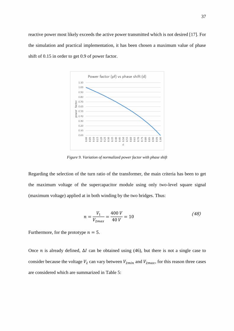
37
reactive power most likely exceeds the active power transmitted which is not desired [17]. For
the simulation and practical implementation, it has been chosen a maximum value of phase
shift of 0.15 in order to get 0.9 of power factor.
Figure 9. Variation of normalized power factor with phase shift
Regarding the selection of the turn ratio of the transformer, the main criteria has been to get
the maximum voltage of the supercapacitor module using only two-level square signal
(maximum voltage) applied at in both winding by the two bridges. Thus:
𝑛 =𝑉1
𝑉2𝑚𝑎𝑥=
400 𝑉
40 𝑉= 10
(48)
Furthermore, for the prototype 𝑛 = 5.
Once 𝑛 is already defined, ∆𝐼 can be obtained using (46), but there is not a single case to
consider because the voltage 𝑉2 can vary between 𝑉2𝑚𝑖𝑛 and 𝑉2𝑚𝑎𝑥, for this reason three cases
are considered which are summarized in Table 5:

38
Table 5. Values of ∆𝐼
Condition of 𝑽𝟐 at Pmax ∆𝑰 for Simulation ∆𝑰 for Experimental
𝑉2 = 𝑉2𝑚𝑖𝑛 254.90 A 16.99 A
𝑉2 = 0.75 ∗ 𝑉2𝑚𝑎𝑥 124.18 A 8.28 A
𝑉2 = 𝑉2𝑚𝑎𝑥 58.82 A 3.92 A
As it is described in [4], the range of voltage of supercapacitors can vary between 𝑉2𝑚𝑖𝑛 and
𝑉2𝑚𝑎𝑥. The controller of the system should be able to keep the voltage around an intermediate
voltage, defined previously as 0.75 ∗ 𝑉2𝑚𝑎𝑥. Hence, for designing purposes, the rated active
power is guaranteed for the intermediate voltage. Thus, the value of the leakage inductance
required by the system can be obtained as follows:
𝐿 =𝑇𝑆
2∆𝐼(𝑉1 + 𝑛𝑉2(2𝑑 − 1))
(49)
Considering that 𝑓𝑠 =1
𝑇𝑆, the expression becomes:
𝐿 =1
2𝑓𝑠∆𝐼(𝑉1 + 𝑛𝑉2(2𝑑 − 1))
(50)
As it can be seen in (50) the leakage inductance required is also depending on the switching
frequency (𝑓𝑠). For this reason, Figure 10 presents the relationship between the leakage
inductance required by the DAB and the switching frequency at which the system should
operate.

39
Figure 10. Leakage inductance required by the DAB for simulation purposes (left) for prototype (right)
From the previous graphs, it can be seen that when the switching frequency increases, the
inductance required decreased. Since one of the approach of the of this project is not to use an
external inductance, the leakage inductance of the transformer must be as high as possible, the
first chose of frequency is the highest within the range allowed. Therefore, while for simulation
it is chosen 5 kHz as switching frequency and the leakage inductance must be 153 µH, for the
prototype the frequency selected is 20 kHz and the leakage inductance of the transformer
ideally must be 86 uH.
3.4. Design of the high frequency transformer for the prototype
Design a high frequency transformer can become a simple or a very challenging task depending
on the requirements that the transformer need to meet. This is because there are several
parameters which need to be taken into account and optimized. At the same time there are
several approaches to complete the design. For instance, while in [19] the area-product
approach, based on the core geometrical constant (𝐾𝑔), is shown, in [21] is presented a more
general approach, based on the geometrical constant (𝐾𝑔𝑓𝑒) a measure of the effective magnetic
size of core in a transformer design application. This allows to determine the operating flux
density that minimizes the total power loss due to the core and copper [21]. The method

40
selected for this project has been which is based on 𝐾𝑔𝑓𝑒. The design of the transformer has
been obtained following the procedure presented in Figure 3.
First of all, several parameters are stated and listed:
a) Since the switching frequency chosen for the prototype is 20 kHz, ferrite is the most
recommended material to use [19].
b) The wire material is copper; therefore, its resistivity is 1.72e-6 Ωcm
c) For the total rms winding current (𝐼𝑡𝑜𝑡), it has been used the following expression:
𝐼𝑡𝑜𝑡 =𝑛1
𝑛1𝐼1 +
𝑛2
𝑛1𝐼2 = 𝐼1 +
1
𝑛𝐼2
(51)
The primary rms current (𝐼1 = 𝐼𝑖𝑛𝑟𝑚𝑠) has been obtained from (34) ensuring the maximum
active power (100 kW) at maximum phase shift allowed (𝑑 = 0.15), considering 𝑉1 = 60𝑉,
𝑛 = 5, 𝑓𝑠 = 20𝑘𝐻𝑧 and 75% of the maximum supercapacitor terminal voltage (𝑉2 = 9𝑉). The
value calculated has been 𝐼1 = 2.455 𝐴.
Then, taking into account the turn ratio (𝑛), the secondary rms current (𝐼2) is equal to
𝐼2 = 𝑛𝐼2 = 5(2.455)𝐴 = 12.27 𝐴 (52)
Then, the total rms winding current, referred to the primary, is
𝐼𝑡𝑜𝑡 = 2.455 +1
512.27 = 4.91 𝐴
(53)
d) In the Figure 11, it can be seen the applied primary volt-seconds (𝜆1) for the square
waveform applied to the high voltage bridge.

41
Figure 11. Transformer primary voltage waveform, illustration the volt-second applied during the positive
portion of the cycle
𝜆1 = 𝑉1 ∗𝑇𝑆
2= 𝑉1 ∗
1
2𝑓𝑠= 60 ∗
1
2 ∗ 20000= 0.0015 [𝑉𝑠]
(54)
e) In addition, since the maximum power of the system is 100 W, it is assumed the total power
dissipation by the transformer 𝑃𝑡𝑜𝑡 = 1 𝑊 as well as the winding fill factor 𝐾𝑢 = 0.3, value
which is recommended to be used in [19] for ferrite cores. Also, the core loss exponent (𝛽)
has been set as 2.6, based on the information provided in [21] for ferrite materials.
f) In order to calculate core losses (𝑃𝑓𝑒), it is necessary to know the value of the core loss
coefficient 𝐾𝑓𝑒. Note that 𝐾𝑓𝑒 increases its value when the switching frequency is also be
increased. Using the technical information of the core provided by the supplier, 𝐾𝑓𝑒 has
been obtained approximately for 20 kHz. For N97 ferrite core material the value obtained
is 5.91 𝑊/𝑐𝑚3𝑇𝛽 .
The next step in the design transformer is to calculate the threshold of 𝐾𝑔𝑓𝑒, then:
𝐾𝑔𝑓𝑒𝑡ℎ𝑟𝑒𝑠=
𝜌𝜆12𝐼𝑡𝑜𝑡
2 𝐾𝑓𝑒(2/𝛽)
4𝐾𝑢(𝑃𝑡𝑜𝑡)((𝛽+2)/𝛽)108
(55)
Therefore,
𝐾𝑔𝑓𝑒𝑡ℎ𝑟𝑒𝑠=
(1.72𝑥10−6)(0.0015)2(4.91)2(5.91)(2/2.6)
4(0.3)(1)((2.6+2)/2.6)108 = 0.023
(56)

42
Now the it is necessary to find a specific core material and its corresponding geometry whose
𝐾𝑔𝑓𝑒 is greater than 𝐾𝑔𝑓𝑒𝑡ℎ𝑟𝑒𝑠 obtained previously. There are several geometries which meet
this condition. However, due to availability ETD-59 geometry has been chosen whose physical
dimensions, given by Ferroxcube supplier, are listed in Table 6.
Table 6. Core dimensions
Parameter ETD-59 - N97
Core cross-sectional area (𝐴𝐶) 3.68 𝑐𝑚2
Core window area (𝑊𝐴) 3.66 𝑐𝑚2
Mean length per turn (𝑀𝐿𝑇) 10.6 𝑐𝑚
Magnetic path length (𝑙𝑚) 13.9 𝑐𝑚
Suppliers of cores usually do not provide the value of 𝐾𝑔𝑓𝑒 directly, but it can be computed
from other known parameters.
𝐾𝑔𝑓𝑒 =𝑊𝐴 (𝐴𝐶)(2(𝛽−1)/𝛽)
(𝑀𝐿𝑇)𝑙𝑚(2/𝛽)
((𝛽
2)
−(𝛽
𝛽+2)
+ (𝛽
2)
(2
𝛽+2)
)
−(𝛽+2
𝛽)
(57)
The expression can also be written
𝐾𝑔𝑓𝑒 =𝑊𝐴 (𝐴𝐶)
(2(𝛽−1)
𝛽)
(𝑀𝐿𝑇)𝑙𝑚
(2𝛽
)𝑢(𝛽)
(58)
Since 𝛽 = 2.6, then 𝑢(𝛽) = 0.298. Then,
𝐾𝑔𝑓𝑒 = 0.0675 (59)

43
The result shows that the condition 𝐾𝑔𝑓𝑒 ≥ 𝐾𝑔𝑓𝑒𝑡ℎ𝑟𝑒𝑠 is met. Therefore, the selection of the
core is done. The next step is to evaluate the peak ac flux density using next equation:
𝛥𝐵 = (108𝜌𝜆1
2𝐼𝑡𝑜𝑡2
2𝐾𝑢
(𝑀𝐿𝑇)
𝑊𝐴𝐴𝐶3 𝑙𝑚
1
𝛽𝐾𝑓𝑒)
(1
𝛽+2)
(60)
Then,
𝛥𝐵 = 0.105 𝑇 (61)
As it can be seen, the value obtained of Δ𝐵 is lower than the 𝐵𝑠𝑎𝑡 of the N97 ferrite material,
which is around 400 mT. Furthermore, there is an adequate margin between those values. This
is important because the risk of getting transformer core saturation is low.
Following with the design, the next step has been to evaluate the number of turns for the
primary side.
𝑛1 =𝜆1
2𝛥𝐵𝐴𝐶104 =
0.0015 𝑉𝑠
2(0.105 𝑇)(3.68 𝑐𝑚2)104 = 21.85
(62)
Since the number of turns must be an integer, it has been set 𝑛1 = 25. Thus, the new value of
Δ𝐵 = 0.081 𝑇 and that is also acceptable. Now, the number of turns for the secondary is
obtained:
𝑛2 =𝑛1
𝑛=
25
5= 5
(63)
According the procedure presented in Figure 3, the next step is to evaluate the fraction of
window area allocated to each winding. From equations presented in [21], those fraction can
be calculated:

44
𝛼1 =𝑛1𝐼1
𝑛1𝐼𝑡𝑜𝑡=
2.455
4.91= 0.5
(64)
𝛼2 =𝑛2𝐼2
𝑛1𝐼𝑡𝑜𝑡=
5(12.27)
25(4.91)= 0.5
(65)
It is clear to see and understand that 𝛼1 and 𝛼2 are the same because in the secondary side,
there is only one winding. These coefficients can change when the secondary has more than
one winding.
In order to determine the wire size, it has been used expressions also given in [21].
𝐴𝑤1 ≤𝛼1𝐾𝑢𝑊𝐴
𝑛1=
0.5(0.3)(3.66 𝑐𝑚2)
25= 0.0289
(66)
𝐴𝑤2 ≤𝛼2𝐾𝑢𝑊𝐴
𝑛2=
0.5(0.3)(3.66 𝑐𝑚2)
5= 0.144
(67)
The commercial wire gauge is selected using the wire table included in the Appendix D of [21],
then for the primary AWG #16 has area 13.07𝑥10−3𝑐𝑚2 and it is suitable for the primary
winding. On the other hand, for the secondary winding, the AWG #10 has area
52.41𝑥10−3𝑐𝑚2 and it should be fine. However, this is not a practical solution because
proximity effect appears and significant losses can be got. Another fact to be considered is the
skin effect, because the maximum frequency for 100% skin depth for solid conductor copper
for AWG #10 is 2600Hz only [28]. Therefore, there are some options: interleaved foil
windings, Litz wire or several parallel strands of smaller wire [21]. Because of the cost and
availability, the third option has been used. In order to define the number of strands, it has been
taken the ratio between the areas of the wires, as follows:
𝑚 =52.41𝑥10−3𝑐𝑚2
13.07𝑥10−3𝑐𝑚2= 4
(68)

45
The winding geometry is crucial in order to get low or high values of leakage inductance in the
transformer. Several researches have been developed which have combined different winding
arrangements [5], [29], [30], [9] as well as modification of the cores adding a ferrite flux
diverter [5] or a leakage layer [9]. Due to the time and complexity of modifying physically the
core, only the winding arrangement has been considered. In [29], four winding configurations
were analyzed and also the leakage inductance were calculated and obtained by simulation. It
can be seen that the highest leakage inductance is achieved when the primary and secondary
winding are not interleaved (refer to Figure 12). Therefore, this winding configuration has
been chosen for the transformer.
Figure 12. Non interleaved winding configuration (reprinted from [29])
Another fact considered has been the size of the insulation thickness. In [19], it is shown that
when the insulation thickness increases, the leakage inductance also increases. Practically,
during the construction of the transformer several turns of insulated tape were added.
Figure 13 shows the transformer which has been built. In order to avoid core saturation during
transient periods, a very thin airgap in each leg of the core geometry and a piece of paper sheet
has been introduced.

46
Figure 13. Transformer built for the prototype
3.4.1. Ideal magnetizing inductance estimation
In order to estimate the ideal magnetizing inductance required by the transformer to meet the
maximum power (neglecting the resistance due to the copper and leakage inductance), the ideal
magnetizing inductance required can be calculated. Then:
Figure 14. Model of the transformer neglecting copper resistance and leakage inductance
𝑣𝑎𝑐1𝑟𝑚𝑠= 2𝜋𝑓𝑠𝐿𝑚𝐼𝑚𝑟𝑚𝑠
(69)
In addition,
𝑃𝑚𝑎𝑥 = 𝑣𝑎𝑐1𝑟𝑚𝑠𝐼𝑁𝑟𝑚𝑠
(70)
For simulation purposes:
𝐼𝑁𝑟𝑚𝑠=
𝑃𝑚𝑎𝑥
𝑣𝑎𝑐1𝑟𝑚𝑠
=10000
400= 25𝐴
(71)
For the prototype:

47
𝐼𝑁𝑟𝑚𝑠=
𝑃𝑚𝑎𝑥
𝑣𝑎𝑐1𝑟𝑚𝑠
=10000
400= 1.6𝐴
(72)
Considering a magnetizing inductance equal to 0.2 times the rated value of the current (𝐼𝑁𝑟𝑚𝑠),
the result for simulation is:
𝐼𝑚𝑟𝑚𝑠= 5𝐴 (73)
𝐿𝑚 =𝑣𝑎𝑐1𝑟𝑚𝑠
2𝜋𝑓𝑠𝐼𝑚𝑟𝑚𝑠
=400
2𝜋(5000)(5)= 2.55 𝑚𝐻
(74)
For the prototype is:
𝐼𝑚𝑟𝑚𝑠= 0.32𝐴 (75)
𝐿𝑚 =𝑣𝑎𝑐1𝑟𝑚𝑠
2𝜋𝑓𝑠𝐼𝑚𝑟𝑚𝑠
=60
2𝜋(20000)(0.32)= 1.49 𝑚𝐻
(76)
3.4.1. Magnetizing and leakage inductance estimation of the transformer
In terms of implementation, after building the transformer, it has been applied a square
waveform of voltage in the primary side to see the response of the magnetizing inductance. As
it was expected that the transformer is operating out of the saturation region and the linear
shape of the magnetizing current is shown in Figure 15 which demonstrates that this is the case.
Figure 15. Voltage and current applied on the magnetizing inductance

48
The scale of 𝐼𝑚 in the Figure 15 is in volts because it was used a 1 Ω shunt resistor. Then Δ𝐼𝑚
is 1.26 A. As a result of this:
𝑣𝑎𝑐1 = 𝑣𝐿𝑚= 𝐿𝑚
𝛥𝐼𝑚
𝛥𝑡
(77)
Then,
𝐿𝑚 =𝛥𝑡
𝛥𝐼𝑚𝑣𝐿𝑚
=𝑇𝑠
2𝛥𝐼𝑚𝑣𝐿𝑚
=𝑣𝐿𝑚
2𝑓𝑠𝛥𝐼𝑚=
60
2(20000)(1.26)= 1.19𝑚𝐻
(78)
Finally, using the LCR meter HM8018, the magnetizing and leakage inductance has been
measured approximately as Figure 16 shows. The value obtained is 1.34 mH at 10 kHz. The
leakage inductance has been also measured, however, since the turn ratio is not 1:1 the measure
is not completely real, but at least it gives an approximation. Then, the value obtained is
10.5µH.
Figure 16. Schematic to measure approximately the magnetizing inductance (left) and the leakage inductance
(right) using the LCR meter HM8018
3.4.2. Turn radio of the transformer
Once the transformer was build, the turn ratio has been obtained dividing the peak to peak
sinusoidal voltage applied to the primary (21.6 V) and the secondary side of the transformer
(4.64 V). Therefore, 𝑛 = 4.65.

49
Figure 17. Primary and secondary sinusoidal voltages applied to the transformer
3.5. Selection of the Controller
In order to generate the control signals to operate the H bridges, the Texas Instrument DSP
TMS320F28335 has been used (Figure 18). Aside from its high clock frequency operation (150
MHz), this processor gives several enhanced features which are useful to implement the PWM
signals as well as read and convert analogue data to complete the control loop. This is because
internally, this processor already supports dead times, phase shifts and obviously the duty cycle
control. In terms of ADC conversion, the processor includes IEEE-754 Single-Precision
Floating-Point Unit (FPU), then the manipulation of floating point data is easier. In order to
implement the control algorithm, Code Composer Studio version 6.1.3 has been used. This
software is provided by Texas Instrument and includes a powerful debugging tool.
Figure 18. Texas Instrument DSP TMS320F28335

50
3.1. Isolation of control signals for gating power devices
In order to isolate the control signals generated by the DSP, it is necessary to use an additional
stage for each power device, which has been implemented using the isolated IGBT/MOSFET
gate drive HCPL-3120.
Figure 19. Recommended LED Drive and Application Circuit (based on [31])
The value of the resistance 𝑅𝑔 has been obtained the recommendation given in the application
note [31].
𝑅𝑔 ≥𝑉𝐶𝐶 − 𝑉𝑂𝐿
𝐼𝑂𝐿𝑃𝐸𝐴𝐾=
15 − 2
2.5= 5.2 𝛺
(79)
In order to meet the conditions, then, it has been chosen 15 Ω as 𝑅𝑔. On the other hand, the
power source 𝑉𝐶𝐶 = 15𝑉 has been obtained using the NMA0515SC which is an Isolated 1W
Dual Output DC/DC Converters. The value of 𝑉𝐶𝐶 = 15𝑉 was chosen according the
specification of 𝑉𝐺𝑆𝑀𝐴𝑋 which is ±20𝑉 for IRF530 and ±18𝑉 STP36NF06L.

51
3.2. Selection of the Power Devices
On the HV side, the rated voltage to be handled is 60V and the maximum input current is
4.79A. Therefore, the MOSFET IRF530 has been chosen. This device handles 100 V as Drain-
Source breakdown voltage, 14 A as maximum continuous Drain current and 0.16 Ω as Drain-
Source On-State resistance.
On the LV side, the maximum voltage to be handled is 12V. However, due to overvoltage
spikes during switching and availability, a set of MOSFETs with a Drain-Source breakdown
voltage equal to 60 V are selected. In terms of current, due to the ripple, the maximum output
current is 23.95A. Then, the MOSFET STP36NF06L is selected which handles 30 as Drain-
current. It has a low on-state resistance, only 40 mΩ.
Figure 20 shows the Drain-Source voltage (VDS) taken from one of the MOSFET of HV bridge
and LV bridge when a resistive-inductive load was connected to each bridge independently. It
can be seen a high ripple and oscillations during the commutation.
Figure 20. Drain-Source voltage (𝑉𝐷𝑆) of a mosfet (left) HV bridge, and (right) LV bridge
In order to reduce the overshoot seen in Figure 20, it has been required to add an electrolytic
and a film capacitor in HV bridge and LV bridge. While the electrolytic capacitor normally is
used to compensate variations because of an unstable power source, the film capacitor, also

52
called decoupling capacitor, helps to reduce the noise and oscillations. The values were defined
after several trial and error tests. Table 7 gives a summary of the capacitors used.
Table 7. Summary of electrolytic and film capacitors used for HV and LV bridges.
Bridge Capacitor Capacitance Voltage
High voltage Electrolytic 470 uF 400 V
Film 0.33 uF 250 V
Low voltage Electrolytic 2200 uF 63 V
Film 0.33 uF 250 V
Figure 21 shows the resulting waveforms of gate-source voltages once the capacitors have been
included. It can be noticed a considerable reduction of the overshoot detected before.
Figure 21. Date-Source voltage (𝑉𝐷𝑆) of a mosfet (left) HV bridge, and (right) LV bridge
3.3. Snubbers
Once the two bridges are interconnected by means the high frequency transformer, it has been
tested again the commutation of the MOSFETs in each bridge. Figure 22 shows the Gate-
Source voltages (VGS) and it can be seen that there is a lot of ringing caused by the recovery-
induced oscillations [22].

53
Figure 22. Period of ringing frequency (𝑓𝑝) of 𝑉𝐷𝑆 for a MOSFET in (left) HV bridge, and (right) LV bridge
Then, a RCD snubber circuit for each MOSFET is required to minimized the oscillations. By
knowing the parasitic capacitance (𝐶𝑝) taken from the datasheet of the MOSFET, the snubber
capacitance (𝐶𝑠𝑛𝑏) will be within the range of 0.5 to 2 times the parasitic capacitance [22].
From Figure 22, the ringing frequency (𝑓𝑝) is measured for each set of MOSFETs and the
snubber resistance (𝑅𝑠𝑛𝑏) can be estimated as follows:
𝑅𝑠𝑛𝑏 =1
4𝜋𝑓𝑝𝐶𝑝
(80)
In addition, the wattage of 𝑅𝑠𝑛𝑏 is calculated with:
𝑃𝑠𝑛𝑏 =1
2𝐶𝑠𝑛𝑏𝑉𝑠𝑛𝑏
2 𝑓𝑠 (81)
Then, taking into account measurements, availability of elements in the laboratory and some
trial and error test, the elements of the RCD snubber circuits are summarized in Table 8.
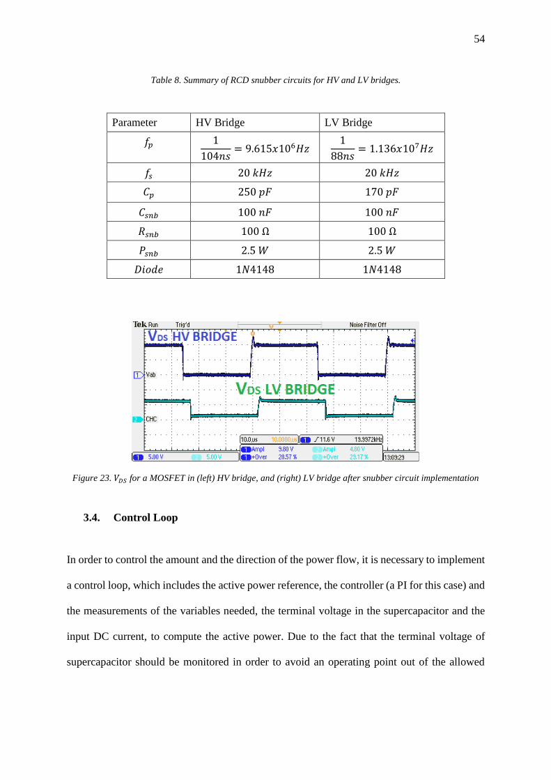
After implementing the snubber circuit for each MOSFET, the resulting waveforms are
presented in Figure 23 where it is notorious the reduction of the ringing and the overshoot of
𝑉𝐷𝑆 in MOSFETs from HV and LV bridges.
54
Table 8. Summary of RCD snubber circuits for HV and LV bridges.
Parameter HV Bridge LV Bridge
𝑓𝑝 1
104𝑛𝑠= 9.615𝑥106𝐻𝑧
1
88𝑛𝑠= 1.136𝑥107𝐻𝑧
𝑓𝑠 20 𝑘𝐻𝑧 20 𝑘𝐻𝑧
𝐶𝑝 250 𝑝𝐹 170 𝑝𝐹
𝐶𝑠𝑛𝑏 100 𝑛𝐹 100 𝑛𝐹
𝑅𝑠𝑛𝑏 100 Ω 100 Ω
𝑃𝑠𝑛𝑏 2.5 𝑊 2.5 𝑊
𝐷𝑖𝑜𝑑𝑒 1𝑁4148 1𝑁4148
Figure 23. 𝑉𝐷𝑆 for a MOSFET in (left) HV bridge, and (right) LV bridge after snubber circuit implementation
3.4. Control Loop
In order to control the amount and the direction of the power flow, it is necessary to implement
a control loop, which includes the active power reference, the controller (a PI for this case) and
the measurements of the variables needed, the terminal voltage in the supercapacitor and the
input DC current, to compute the active power. Due to the fact that the terminal voltage of
supercapacitor should be monitored in order to avoid an operating point out of the allowed

55
voltage range, an additional stage has been included. Figure 24 shows the block diagram used
for simulation purposes.
Figure 24. Control loop for simulation purposes
Because of the time, the small signal model of the DAB has not been presented in the report.
Therefore, the PI controller has been set after many trial and error simulations. The output of
the control loop is 𝑑 , which is the phase shift between the HV and LV bridges. Moreover, a
limiter block has been included in order to limit the maximum phase shift to 0.15.
On the other hand, 𝐸𝑛𝑎𝑏𝑙𝑒 signal activate or deactivate the operation of the H-bridges
depending on the terminal voltage of the supercapacitors and the reference of the power flow.

56
3.4.1. Sensing the supercapacitor voltage
The supercapacitor voltage is one of the variables that has to be measured and feedback to
complete the power flow control algorithm. For measuring this variable, the HCPL-7840
isolation amplifier circuit has been used. To set the input voltage to the HCPL-7840 and
adequate voltage divider has been used (refer Figure 25). Then, according the circuit suggested
in the application noted provided by the supplier has been used to get a differential output
voltage on the other side of the HCPL-7840 optical isolation barrier, where the differential
output voltage is proportional to the terminal voltage of the string of supercapacitors. In the
input side of the isolation amplifier circuit has been used a low-pass (RC) filter formed by 68
Ω resistor and 0.01uF capacitor also recommended by the supplier.
Figure 25. First stage of the circuit for sensing the supercapacitor voltage
A second stage of signal conditioning (Figure 26) has been introduced in order to limit the
voltage range to be sensed between 6 to 12 V only. In addition, a 3.0 V Zener diode was used
to clamp the maximum voltage going to the DSP as 3.0 V.

57
Figure 26. Second stage of the circuit for sensing the supercapacitor voltage
Table 9 shows the values of the voltages measured at each point of the circuit after
implementing two stages of conditioning signal of voltage of the supercapacitor string
𝑉2.
Table 9. Voltages measured at each point of the circuit used to sense the voltage of the supercapacitor string
𝑽𝟐 𝑽𝑹𝑩 𝑽𝟕−𝟔 𝑽𝑶𝑼𝑻𝟏 𝑽𝑺𝑪 (𝒕𝒐 𝒕𝒉𝒆 𝑫𝑺𝑷)
6.00 0.05 0.39 -1.51 0.02
7.00 0.06 0.45 -1.76 0.52
8.00 0.07 0.52 -2.01 1.02
9.00 0.07 0.58 -2.26 1.53
10.00 0.08 0.64 -2.51 2.03
11.00 0.09 0.71 -2.77 2.53
12.00 0.10 0.77 -3.02 3.09
3.4.1. Sensing the input current
Another variable which needs to be sensed is the current flowing through the converter. There
are several options. The current can be measured in the HV side or LV side, in the DC or AC
side. Since the turn ratio ideally is equal to 5, the value of the AC and DC currents in the LV
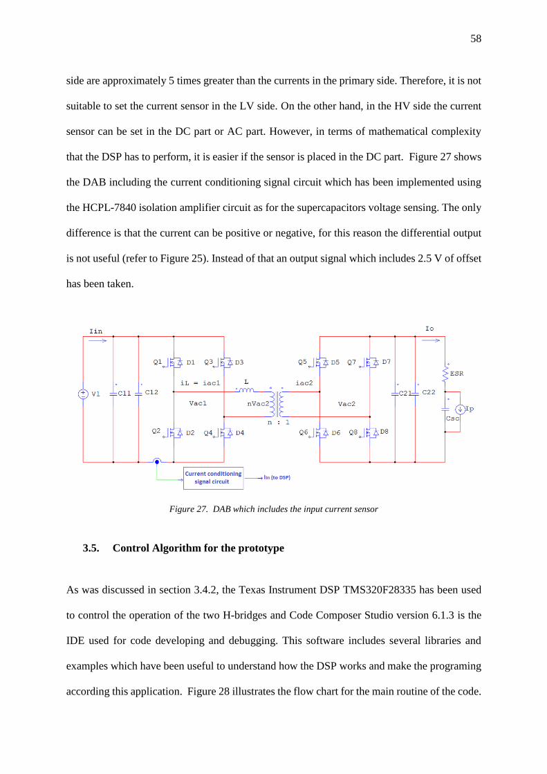
58
side are approximately 5 times greater than the currents in the primary side. Therefore, it is not
suitable to set the current sensor in the LV side. On the other hand, in the HV side the current
sensor can be set in the DC part or AC part. However, in terms of mathematical complexity
that the DSP has to perform, it is easier if the sensor is placed in the DC part. Figure 27 shows
the DAB including the current conditioning signal circuit which has been implemented using
the HCPL-7840 isolation amplifier circuit as for the supercapacitors voltage sensing. The only
difference is that the current can be positive or negative, for this reason the differential output
is not useful (refer to Figure 25). Instead of that an output signal which includes 2.5 V of offset
has been taken.
Figure 27. DAB which includes the input current sensor
3.5. Control Algorithm for the prototype
As was discussed in section 3.4.2, the Texas Instrument DSP TMS320F28335 has been used
to control the operation of the two H-bridges and Code Composer Studio version 6.1.3 is the
IDE used for code developing and debugging. This software includes several libraries and
examples which have been useful to understand how the DSP works and make the programing
according this application. Figure 28 illustrates the flow chart for the main routine of the code.

59
START
Include libraries
Declare Prototype statements, functions and interruptions
Declare Prototype statements, functions and interruptions
Declare Variables
Define constants used to set the switching frequency and initial duty cycle, maximum
phase shift
Initialize System Control, GPIO, EPWM1-4 pins as outputs, ADC module.
Enable interrupts
Enable global interrupts
Configure the ADC conversion
Configure EPWM1 to EPWM4
END
Set the Enable signal based on the Figure 24 control algorithm
Figure 28. Flow chart of the main program for the DSP
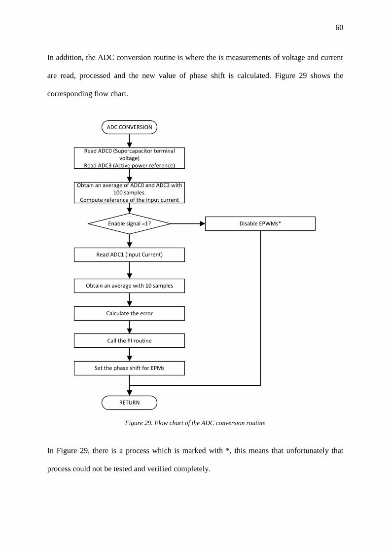
60
In addition, the ADC conversion routine is where the is measurements of voltage and current
are read, processed and the new value of phase shift is calculated. Figure 29 shows the
corresponding flow chart.
ADC CONVERSION
Read ADC0 (Supercapacitor terminal voltage)
Read ADC3 (Active power reference)
Read ADC1 (Input Current)
Obtain an average with 10 samples
Enable signal =1?
Call the PI routine
Disable EPWMs*
Set the phase shift for EPMs
Calculate the error
RETURN
Obtain an average of ADC0 and ADC3 with 100 samples.
Compute reference of the Input current
Figure 29. Flow chart of the ADC conversion routine
In Figure 29, there is a process which is marked with *, this means that unfortunately that
process could not be tested and verified completely.

61
4. Simulation Results and Discussion
4.1. Open Loop Results
While Figure 30 illustrates the waveforms obtained for an ideal supercapacitor, Figure 31
shows the same waveforms taking into account the ESR and Ip which are part of its model and
obtained from the designing section. From those results, it can be concluded that ESR is a very
important parameter which affects the behavior of the DAB, especially for the inductor current.
In order to reduce ESR, several parallel cells must be included. Figure 32 shows the result when
5 parallel cells have been connected and the new ESR is 30mΩ. For a real system, the design
process an iterative process is performed.
Figure 30. DAB results for ideal supercapacitor (constant capacitance, ESR=0, Ip=0A).

62
Figure 31. DAB results for string of supercapacitor (constant capacitance, ESR=150mΩ, Ip=260uA).
Figure 32. DAB results for string of supercapacitor (constant capacitance, ESR=30mΩ, Ip=1300uA).

63
4.2. Close Loop Results
4.2.1. Tracking of Supercapacitor Voltage for different values of ESR
As was described in Section 4.1, ESR affects the supercapacitor voltage waveform. For low
values of ESR (units of miliomhs or less), waveform is linear but when the ESR is higher the
ripple increases. Figure 33 shows the supercapacitor voltage (𝑉𝑜𝑢𝑡 = 𝑉2) when ESR is 0.5 mΩ
(left) and 5 mΩ (right). It can be noticed a linear response as was expected. In addition, it is
included the reference current (𝐼1_𝑟𝑒𝑓) and the signal which is feedback (𝐼1_𝑚𝑒𝑎𝑠𝑢𝑟𝑒𝑑) instead of
the power flow signals because they are proportional.
Figure 33. Supercapacitor voltage (𝑉𝑜𝑢𝑡 = 𝑉2) when ESR is 0.5 mΩ (left) and 5 mΩ (right).
4.2.1. Supercapacitor voltage (𝑽𝒐𝒖𝒕 = 𝑽𝟐) when reaches 𝑽𝟐_𝒎𝒂𝒙 or 𝑽𝟐_𝒎𝒊𝒏
The algorithm for controlling the power flow and monitoring the supercapacitor voltage has
been implemented in order to disable the control signals for two H-bridges when 𝑉2_𝑚𝑎𝑥 or
𝑉2_𝑚𝑖𝑛 are reached. Figure 34 and Figure 36 illustrate small periods of time when the control
signals are disabled, after that the reference of power is changed and the control algorithm starts
to generate signals again (refer to Figure 35 and Figure 37).

64
Figure 34. Supercapacitor voltage (𝑉𝑜𝑢𝑡 = 𝑉2) when reaches 𝑉2_𝑚𝑎𝑥
Figure 35. Control algorithm when 𝑉2_𝑚𝑎𝑥 is reached and power reference is changed.
Figure 36. Supercapacitor voltage (𝑉𝑜𝑢𝑡 = 𝑉2) when reaches 𝑉2_𝑚𝑖𝑛
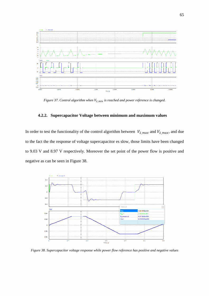
65
Figure 37. Control algorithm when 𝑉2_𝑚𝑖𝑛 is reached and power reference is changed.
4.2.2. Supercapacitor Voltage between minimum and maximum values
In order to test the functionality of the control algorithm between 𝑉2_𝑚𝑎𝑥 and 𝑉2_𝑚𝑎𝑥, and due
to the fact the the response of voltage supercapacitor es slow, those limits have been changed
to 9.03 V and 8.97 V respectively. Moreover the set point of the power flow is positive and
negative as can be seen in Figure 38.
Figure 38. Supercapacitor voltage response while power flow reference has positive and negative values

66
4.2.3. Power Losses
When the converter is working at rated power, the input and output power has been measured.
This is because it is possible to determine the power losses for the system. This result has been
obtained using the parameters of the prototype and a neglected ESR. Then the 𝑃𝑟𝑒𝑓 = 100𝑊,
after simulation Figure 39 shows that the input power is 99.32 W and output power is 95 W.
As a result of these values the efficiency is 95%.
Figure 39. Comparison of Pin and Pout when the Pref is positive
On the other hand, if 𝑃𝑟𝑒𝑓 = −100𝑊, running simulation the efficiency results dividing 98.33
W and 109.26 W, as can be seen in Figure 40, 90%.
Figure 40. Comparison of Pin and Pout when the Pref is negative

67
5. Experimental Results and Discussion
The experimental prototype was implemented practically from scratch. Therefore, at the
beginning, the isolation circuit and H-bridges were inmplemented in the breadborad as Figure
41 shows.
Figure 41. Two H-bridges implemented in breadboard
Once each bridge was working properly and individually, they were transfer to a solderable
breadboard, including decoupling capacitors according supplier’s recommendations, heat sinks
for the MOSFETs and connectors. While Figure 42 illustrates the H-bridge for the HV side,
Figure 43 shows H-bridge for the LV side.

68
Figure 42. H-bridge for the HV side
Figure 43. H-bridge for the LV side
Using a RL load, it was tested again the operation of each bridge individually. Figure 44 shows
the output waveforms of them. Since each H-bridge was designed for different rated voltages
and currents, two individual power sources were used to complete this activity.

69
Figure 44. 𝑣𝑎𝑐1 and 𝑣𝑎𝑐2 tested with different power sources and RL load
Then, the high frequency transformer was connected between two bridges to have the DAB.
Unfortunately, when a constant phase shift was set, at very low voltages of 𝑉1, such as 10 to
15V, a huge interference appeared. As a result of this, the control signals generated by the DSP
were highly affected and the operation of the DAB was wrong. After a lot of testing in order to
detect the source of that interference and solve it, it was found that adding an external
inductance in the secondary side of the transformer the interference decreased. This fact means
that the leakage inductance of the transformer was not enough as was expected.
While higher was the value of the external inductance the interference was better counteract.
Then, other tests were performed in order to get the minimum value required. Due to
availability, a 66.2 µH inductance were selected (see Figure 45).
Figure 45. External inductance of 66.2 µH connected in the LV side
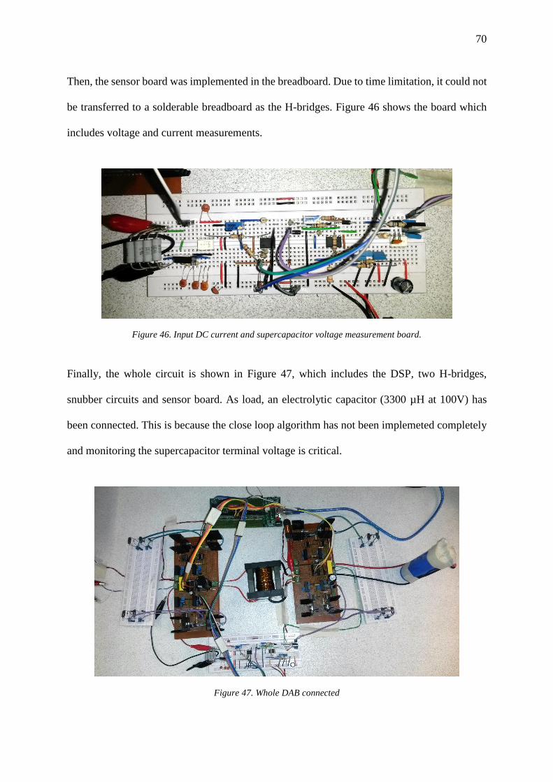
70
Then, the sensor board was implemented in the breadboard. Due to time limitation, it could not
be transferred to a solderable breadboard as the H-bridges. Figure 46 shows the board which
includes voltage and current measurements.
Figure 46. Input DC current and supercapacitor voltage measurement board.
Finally, the whole circuit is shown in Figure 47, which includes the DSP, two H-bridges,
snubber circuits and sensor board. As load, an electrolytic capacitor (3300 µH at 100V) has
been connected. This is because the close loop algorithm has not been implemeted completely
and monitoring the supercapacitor terminal voltage is critical.
Figure 47. Whole DAB connected

71
5.1. Open loop experimental results
Figure 48 depicts the waveforms 𝑖𝐿 , 𝑣𝑎𝑐1 and 𝑣𝑎𝑐2 and obtained for a fix phase shift 𝑑 = 0.128
when the active power flow is from HV side to LV side. It can be noticed that, because of no
voltage control was implemented, 𝑛𝑣𝑎𝑐2 > 𝑣𝑎𝑐1, therefore, the slope of current is negative
when the voltages in two H-bridges have the same sign. In addition, a high spikes are obtained
when MOSFETs commutation are performed. It was noticed that the current test probe used
introduces them.
Figure 48. 𝑖𝐿 , 𝑣𝑎𝑐1 and 𝑣𝑎𝑐2 waveforms tested with a positive phase shift
On the other hand, Figure 49 shows the same waveforms that Figure 48. However, in this case,
the phase shift is negative 𝑑 = −0.128, the active power flow is from LV side to HV side and
𝑛𝑣𝑎𝑐2 < 𝑣𝑎𝑐1, therefore, the slop if the current is the same as was analyzed in section 3.3.
Figure 49. 𝑖𝐿 , 𝑣𝑎𝑐1 and 𝑣𝑎𝑐2 waveforms tested with a negative phase shift

72
5.2. Close loop experimental results
Once the close loop has been implemented some tests were performed. The evolution of the
waveforms is one the first test done. Figure 50 shows vac1, vac2, iL and iin when positive
power flow is required during transient and steady state, left and right pictures respectively.
Although the waveforms are similar to the theoretical ones, it can be seen noise for iL and
undesirable peaks for iin.
Figure 50. 𝑣𝑎𝑐1, 𝑣𝑎𝑐2, 𝑖𝐿 and 𝑖𝑖𝑛 when positive power flow is required (left) transient (right) steady state
The waveform of iL shown in Figure 51 indicates the condition when vac1 ≈ nvac2 and V1 =
25 V. However, it can be noticed that V2 = 21.6 V, therefore 𝑛 ≈ 2.3. This change in the turn
radio apparently is due to the external inductance included in the prototype.
Figure 51. 𝑣𝑎𝑐1, 𝑣𝑎𝑐2, 𝑖𝐿 and 𝑖𝑖𝑛 when positive power flow is required and 𝑣𝑎𝑐1 ≈ 𝑛𝑣𝑎𝑐2

73
Depending on the power flow requirements the supercapacitor voltage increases or decreases
and this variation according the control algorithm should be linear. Figure 52 shows the results
obtained in both cases, left picture for increasing and left one for decreasing. It is also included
Figure 52. Supercapacitor voltage linear response (left) increasing (right) decreasing
When 𝑉2_𝑚𝑎𝑥 or 𝑉2_𝑚𝑖𝑛 are reached the control order in the simulation was to disable the control
signals. However, in the practical implementation, the control order has been to set zero phase
shift, this was done because mores testing is required. Figure 53 shows vac1, vac2, iL and iin
under these conditions.
Figure 53. DAB operation when supercapacitor voltage is lower than 𝑉2_𝑚𝑖𝑛
Figure 54 depicts the primary and secondary voltages during commutation as well as the peak
of input current which appears during this period of time. This peak of current is not desired
and it appears apparently because of the snubber circuits included for each MOSFET. Then,
the power losses have been increased.

74
Figure 54. Duration of input current peak during commutation of HV bridge
6. Conclusion
The DAB converter addressed in this report has several advantages. One of this is the
bidirectional power flow. It is regularly used in ESS which can combine batteries and
supercapacitors. Supercapacitors have been only included in this project.
It can be concluded that theoretical analysis is not as close as it was expected with the real
operation of the DAB, because some phenomena like EMI, resonance due to parasitic elements
are not taken into account.
This report presents some issues during hardware implementations which were overcome
adding an external inductance to the secondary side of the transformer. General speaking a
better performance of the experimental prototype could be obtained using a compact PCB
board which helps to reduce EMI, stray inductances, long parallel wires and ground loops.
Finally, a lot of further work can be addressed with this converter because application such as
electrical vehicles use supercapacitors as ESDs.

75
7. References
[1] F. Pires, E. Romero-Cadaval, D. Vinnikov, I. Roasto y J. F. Martins, «Power converter
interfaces for electrochemical energy storage systems - A review,» Energy Conversion
and Management, vol. 86, pp. 453-475, 2014.
[2] D. Trowler y B. Whitaker, «Bi-Directional Inverterand Energy StorageSystem,»
University of Arkansas, 2008.
[3] P. F. Ribeiro, B. K. Jhonson, M. L. Crow, A. Arsoy y Y. Liu, «Energy Storage Systems
for Advanced Power Applications,» Proceedings of the IEEE, vol. 89, nº 12, December
2001.
[4] P. J. Grbović, P. Delarue y P. Le Moigne, «Selection and design of ultra-capacitor
modules for power conversion applications: From theory to practice,» de Power
Electronics and Motion Control Conference (IPEMC), 2012 7th International, 2012.
[5] D. De, C. Klumpner, M. Rashed, C. Patel, P. Kulsangcharoen y G. Asher, «Achieving
the desired transformer leakage inductance necessary in DC-DC converters for energy
storage applications,» IET Proc. of Power Electronics Machines and Drives Conf.
PEMD’12, nº Paper 213, March 2012.

76
[6] F. Krismer, «Modeling and optimization of bidirectional dual active bridge DC-DC
converter topologies,» 2010.
[7] R. Naayagi, A. Forsyth y R. Shuttleworth, «Bidirectional control of a dual active bridge
DC-DC converter for aerospace applications,» IET Power Electronics, vol. 5, nº 7, pp.
1104 - 1118, 2012.
[8] A. K. Jain y R. Ayyanar, «Pwm control of dual active bridge: Comprehensive analysis
and experimental verification,» IEEE Transactions on Power Electronics, vol. 26, nº 4,
pp. 1215 - 1227, 2011.
[9] B. Cougo y J. W. Kolar, «Integration of Leakage Inductance in Tape Wound Core
Transformers for Dual Active Bridge Converters,» de CIPS 2012, Nuremberg/Germany,
2012.
[10] P. J. Grbovic, Ultra-Capacitors in Power Conversion Systems - Applications, Analysis
and Design from Theory to Practice, Germany: Wiley, 2014.
[11] P. Du y N. Lu, Energy Storage for Smart Grids, Elsevier, 2015.
[12] P. T. Moseley y J. Garche, Electrochemical Energy Storage for Renewable Sources and
Grid Balancing, Amsterdam, Netherlands: Elsevier, 2015.
[13] N. Kularatna, Energy Storage Devices for Electronic Systems - Rechargeable Batteries
and Supercapacitors, Elsevier, 2015.

77
[14] D. Wenzhong Gao, Energy Storage for Sustainable Microgrid, Elsevier, 2015.
[15] H. Zhou, T. Bhattacharya, D. Tran, T. S. Terence y A. M. Khambadkone, «Composite
Energy Storage System Involving Battery and Ultracapacitor With Dynamic Energy
Management in Microgrid Applications,» IEEE Transactions on Power Electronics, vol.
26, nº 3, pp. 923 - 930, 2011.
[16] G. Barone, G. Brusco, A. Burgio, M. Motta y D. Menn, «A dual active bridge dc-dc
converter for application in a smart user network,» de Australasian Universities Power
Engineering Conference, Australia, 2014.
[17] M. N. Gitau, G. Ebersohn y J. G. Kettleborough, «Power processor for interfacing
battery storage system to 725 V DC bus,» Energy Conversion and Management, vol. 48,
p. 871–881, 2007.
[18] Shigenori Inoue y Hirofumi Akagi, «A Bidirectional DC–DC Converter for an Energy
Storage System With Galvanic Isolation,» IEEE Transactions on Power Electronics,
vol. 22, nº 6, November 2007.
[19] C. McLyman y T. William, Transformer and Inductor Design Handbook, Fourth ed.,
CRC Press, 2011.
[20] O. A. Hassan, C. Klumpner y G. Asher , «Design Considerations for Core Material
Selection and Operating Modes for a High Frequency Transformer Used in an Isolated

78
DC/DC Converter,» de Power Electronics and Applications (EPE 2011), Proceedings
of the 2011-14th European Conference on, Birmingham/UK, September 2011.
[21] R. W. Erickson y D. Maksimovic, Fundamentals of Power Electronics, Second ed., New
York: Kluwer Academic Publishers, 2004.
[22] A. A. S. Mohamed, D. Allen, T. Youssef y O. Mohammed, «Optimal design of high
frequency H-bridge inverter for wireless power transfer systems in EV applications,» de
Environment and Electrical Engineering (EEEIC), 2016 IEEE 16th International
Conference on, 2016.
[23] M. Pavlovsky, S. De Hann y J. A. Ferreira., «Winding losses in high current high
frequency transformer foil winding with leakage layer,» IEEE PESC, 2006.
[24] N. Mohan, T. Undeland y W. Robbins, Power electronics: Converters, applications, and
design., Second ed., John wiley and Sons, 1995.
[25] Tecate Group, «www.tecategroup.com,» [En línea]. Available:
https://www.tecategroup.com/app_notes/0_Tecate_Group_Ultracapacitor%20sizing.pd
f. [Último acceso: 15 07 2016].
[26] PowerStor, «www.farnell.com,» [En línea]. Available:
http://www.farnell.com/datasheets/1786661.pdf?_ga=1.170674211.202172677.146461
2771. [Último acceso: 20 07 2016].

79
[27] Z. Zhang, O. C. Thomsen, M. A. E. Andersen, J. D. Schmidt y H. R. Nielsen, «Analysis
and Design of Bi-directional DC-DC Converter in Extended Run Time DC UPS System
Based on Fuel Cell and Supercapacitor,» de Applied Power Electronics Conference and
Exposition, 2009. APEC 2009. Twenty-Fourth Annual IEEE, Denmark, 2009.
[28] Powerstream, «www.powerstream.com,» [En línea]. Available:
http://www.powerstream.com/Wire_Size.htm. [Último acceso: 30 07 2016].
[29] Z. Ouyang, J. Zhang y W. G. Hurley, «Calculation of Leakage Inductance for High-
Frequency Transformers,» IEEE Transactions on Power Electronics, vol. 30, nº 10, pp.
5769 - 5775, 2015.
[30] P. R. Wilson y R. Wilcock, «Frequency Dependent Model of Leakage Inductance for
Magnetic Components,» Advanced Electromagnetics, VOL. X, NO. Y, MONTH 2012,
vol. X, nº Y, 2012.
[31] AVAGO Technologies, «www.avagotech.com,» [En línea]. Available:
http://www.avagotech.com/cs/Satellite?blobcol=urldata&blobheader=application%2Fp
df&blobheadername1=Content-Disposition&blobheadername2=Content-
Type&blobheadername3=MDT-
Type&blobheadervalue1=attachment%3Bfilename%3DAV02-0161EN_DS_HCPL-
3120_2016-03-21.pdf&b. [Último acceso: 01 08 2016].
[32] D. R. Louis, «Practical Magnetic Design: Inductors and Coupled Inductors».
80
[33] K. D. Hoang y J. Wang, «Design optimization of high frequency transformer for dual
active bridge DC-DC converter,» de Electrical Machines (ICEM), 2012 XXth
International Conference on, Marseille, 2012.
[34] M. Amari, I. Khelifi y F. Bacha, «Average model of dual active bridge interfacing ultra-
capacitor in electrical vehicle,» de Renewable Energy Congress (IREC), 2014 5th
International, Hammamet, Tunisia, 2014.
[35] M. A. Bahmani y T. Thiringer, «Accurate Evaluation of Leakage Inductance in High-
Frequency Transformers Using an Improved Frequency-Dependent Expression,» IEEE
Transactions on Power Electronics, vol. 30, nº 10, pp. 5738 - 5745, 2015.
[36] A. Rodríguez Alonso, J. Sebastian, D. G. Lamar, M. M. Hernando y A. Vazquez, «An
overall study of a Dual Active Bridge for bidirectional DC/DC conversion,» de Energy
Conversion Congress and Exposition (ECCE), 2010 IEEE, Gijón, Spain, 2010.