Embed Size (px)
Citation preview

1
ILANA THAISE FIRST – GRR20152613 Departamento de Engenharia Elétrica
Universidade Federal do Paraná
Design of a Wake-up Radio for a Sensor Network
Curitiba - Brazil February 2021

ILANA THAISE FIRST – GRR20152613
Design of a Wake-up Radio for a Sensor Network
Trabalho de Conclusão de Curso de Engenharia Elétrica, Departamento de Engenharia Elétrica, Setor de Tecnologia, Universidade Federal do Paraná.
Orientador: André Augusto Mariano
Curitiba - Brazil February 2021

ILANA THAISE FIRST – GRR20152613
Design of a Wake-up Radio for a Sensor Network
Work presented to the electrical engineering course, from the Federal University of Paraná, as a requirement to obtain the graduation title.
Examining committee
_______________________________________ Prof. PhD. André Augusto Mariano
_______________________________________ Prof. Dr. Luis Henrique Assumpção Lolis
_______________________________________ Prof. Dr. Oscar da Costa Gouveia Filho
Curitiba - Brazil February 2021

ACKNOWLEDGMENT
I would like first of all to address my gratitude to my family for giving me all
the support that I needed during all these years as a student and for always believing
in me and encouraging my dreams.
I also express my deepest thanks to Professors PhD. André Augusto
Mariano and PhD. Thierry Taris, for having advised me and helped me with this
project. I would also like to kindly thank all the professors who contributed to my
education so I could get to where I am, I choose this moment to acknowledge
their contribution gratefully.
Finally, I would like to express my gratitude to everyone who contributed
in some way so that I could fulfill the dream of taking one step closer to obtaining
my engineering diploma and all the friends who made all this process a lot lighter.

ABSTRACT
This study depicts the project of a Wake-up Radio system for a Sensor
Network to operate in a frequency of 900 MHz with an OOK modulation, seeking
ultra-low power consumption, high sensitivity, low data rate and precise selective
awakenings. The used technology is RFCMOS IBM 130 nm and the chosen topologies are
presented in a theoretical foundation section. The steps for defining the each one of
the composing circuits are presented, in addition to the construction of the layouts
of the respective parts in order to build up the WuRx. The results obtained from the
simulations performed on Cadence Virtuoso to evaluate the functioning of the circuits
are shown. In addition, this work is compared with other WuRx developed in the area
and to a PCB version of the same circuit.
During this project, the schematics and layouts of an envelope detector and
a comparator were developed to attain the desired characteristics defined for the
WuRx. The envelope detector is capable of operating with an input voltage of
50 mVp-p, leading to a system input sensitivity of -34 dBm and occupying an area of
96.19 x 52.28 µm2. The comparator has a power consumption of 2.4 nW, occupying
an area of 17.70 x 38.43 µm2.

LIST OF FIGURES
FIGURE 1 – WIRELESS SENSOR NETWORK [1] ................................................. 9
FIGURE 2 – THE ARCHITECTURE OF A WIRELESS SENSOR NETWORK INCLUDING A WURX [1] ....................................................................................... 10
FIGURE 3 – WURX ARCHITECTURE .................................................................. 12
FIGURE 4 – SIGNAL THROUGHOUT A WURX ................................................... 13
FIGURE 5 – LC FILTER APPLIED AS MATCHING NETWORK ........................... 14
FIGURE 6 – EXPECTED OUTPUT SIGNAL FOR AN ENVELOPE DETECTOR .. 14
FIGURE 7 – PASSIVE VOLTAGE MULTIPLIER ................................................... 15
FIGURE 8 – ACTIVE VOLTAGE MULTIPLIER ..................................................... 15
FIGURE 9 – CROSS-COUPLED RECTIFIER ....................................................... 16
FIGURE 10 – INPUT AND OUTPUT VOLTAGES FOR A TRADITIONAL COMPARATOR ..................................................................................................... 17
FIGURE 11 – SIMPLE NMOS COMPARATOR ..................................................... 17
FIGURE 12 – DYNAMIC COMPARATOR ............................................................. 18
FIGURE 13 – INPUT VOLTAGES FOR THE DYNAMIC COMPARATOR............. 19
FIGURE 14 – DYNAMIC COMPARATOR RESET PHASE ................................... 19
FIGURE 15 – DYNAMIC COMPARATOR COMPARAISON PHASE .................... 20
FIGURE 16 – OUTPUT SIGNALS OBTAINED FOR THE DYNAMIC COMPARATOR ..................................................................................................... 20
FIGURE 17 - MEASUREMENTS SETUP .............................................................. 21
FIGURE 18 - SIGNALS MEASURED FOR THE COTS CIRCUIT ......................... 22
FIGURE 19 – FLOWCHART OF THE DEVELOPMENT OF THE WAKE-UP RADIO ............................................................................................................................... 26
FIGURE 20 – VOLTAGE MULTIPLIER RECTIFIER ............................................. 29
FIGURE 21 – CROSS-COUPLED RECTIFIER ..................................................... 29
FIGURE 22 - SINGLE-STAGE CROSS-COUPLED RECTIFIER AND VOLTAGE MULTIPLIER OPERATION.................................................................................... 30
FIGURE 23 - THREE-STAGE CROSS-COUPLED RECTIFIER AND VOLTAGE MULTIPLIER OPERATION.................................................................................... 30
FIGURE 24 – OOK SIGNAL SIMULATION ON CADENCE VIRTUOSO ............... 31

FIGURE 25 - SINGLE-STAGE VOLTAGE MULTIPLIER ENVELOPE DETECTOR OPERATION .......................................................................................................... 32
FIGURE 26 – SINGLE-STAGE CROSS-COUPLED RECTIFIER ENVELOPE DETECTOR OPERATION ..................................................................................... 32
FIGURE 27 - SIMPLE NMOS COMPARATOR ...................................................... 33
FIGURE 28 - SIMPLE NMOS COMPARATOR OPERATION ................................ 34
FIGURE 29 – DYNAMIC LATCH COMPARATOR 1 ............................................. 35
FIGURE 30 – DYNAMIC LATCH COMPARATOR 2 ............................................. 36
FIGURE 31 - CURRENT CALCULATION METHODOLOGY ................................ 37
FIGURE 32 - DYNAMIC LATCH COMPARATOR 1 OPERATION ........................ 38
FIGURE 33 – ENVELOPE DETECTOR LAYOUT ................................................. 39
FIGURE 34 – ZOOM OF THE ENVELOPE DETECTOR LAYOUT ....................... 39
FIGURE 35 – COMPARATOR LAYOUT ............................................................... 40
FIGURE 36 - CIRCUIT MEASUREMENTS COMPARISON .................................. 42

LIST OF TABLES
TABLE 1 : COMPARISON BETWEEN STATE OF THE ART REFERENCES ...... 23
TABLE 2 : VOLTAGE MULTIPLIER RECTIFIER PARAMETERS ......................... 29
TABLE 3 : CROSS-COUPLED RECTIFIER PARAMETERS ................................. 29
TABLE 4 : SIMPLE NMOS COMPARATOR PARAMETERS ................................ 33
TABLE 5 : DYNAMIC LATCH COMPARATOR 1 PARAMETERS ......................... 35
TABLE 6 : DYNAMIC LATCH COMPARATOR 2 PARAMETERS ......................... 36
TABLE 7: ENVELOPE DETECTOR SPECIFICATION .......................................... 41
TABLE 8: COMPARATOR SPECIFICATION ........................................................ 41
TABLE 9 : COMPARISON BETWEEN THIS WORK AND THE STUDIED REFERENCES ...................................................................................................... 43

ACRONYM LIST
ADC - Analog/Digital Converter CDMA - Code-division multiple access CLK - Clock CMOS - Complementary metal-oxide-semiconductor COTS - Components off the shelf f - Frequency GND - Ground HL - High to low I,I - Electric current IBM - International Business Machine IC - Integrated Circuit IoT - Internet of Things L - Length LH - Low to high Nfing - Number of fingers N - Stages NMOS - nFET metal oxide silicon OOK - On-off keying P - Power PCB - Printed Circuit Board PMOS - pFET metal oxide silicon PSS - Periodic steady state Ref - Reference RF - Radio-frequency t - Time USD - US Dolar Vcc - Constant current voltage Vd - Diode threshold voltage Vdd - Supply voltage Vin - Input voltage Vout - Output voltage Vinp - Positive input voltage Vinn - Negative input voltage Vref - Reference voltage Vth - Transistor threshold voltage µC - Micro-controller W - Width WuRx - Wake-up Radio

LIST OF SYMBOLS AND UNITS
A - Ampère °C - Celsius degrees C - Capacitor 𝚫 - Variation D - Diode dB - Decibel F - Farad f - Femto, 10-12 G - Giga, 109
Hz - Hertz k - Kilo, 103
L - Inductor M - Mega, 109 M - Transistor m - Meter m2 - Square meter n - Nano, 10-9
µ - Micro, 10-6
V - Volts Vp-p - Peak to peak voltage W - Ohms

SUMMARY
1 INTRODUCTION ............................................................................................... 9
1.1 MOTIVATION ................................................................................................. 9 1.2 APPLICATIONS ............................................................................................ 10 1.3 OBJECTIVE ................................................................................................. 10
1.3.1 Main Objective ....................................................................................... 10 1.3.2 Specific objectives ................................................................................. 11
2 THEORETICAL FOUNDATION ...................................................................... 12
2.1 CONCEPTS OF A WURX ............................................................................... 12 2.2 CIRCUIT ARCHITECTURE ............................................................................... 13
2.2.1 Matching network .................................................................................. 13 2.2.2 Envelope detector ................................................................................. 14 2.2.3 Comparator ........................................................................................... 16
2.3 CIRCUIT BENCHMARK ................................................................................... 21 2.3.1 COTS circuit .......................................................................................... 21 2.3.2 State of the art references ..................................................................... 22
2.4 SPECIFICATIONS ......................................................................................... 23
3 MATERIALS AND METHODS ........................................................................ 25
4 DEVELOPMENT ............................................................................................. 28
4.1 CIRCUIT DESIGN .......................................................................................... 28 4.1.1 Matching network .................................................................................. 28 4.1.2 Envelope detector ................................................................................. 28 4.1.3 Comparator ........................................................................................... 33
4.2 SUGGESTED CIRCUIT LAYOUT ...................................................................... 38 4.2.1 Envelope detector Layout ...................................................................... 38 4.2.2 Comparator Layout ................................................................................ 40
5 RESULTS ....................................................................................................... 41
6 MARKET POTENTIAL.................................................................................... 44
7 CONCLUSION AND FUTURE WORK............................................................ 45
8 REFERENCES ................................................................................................ 46
9 APPENDIX ...................................................................................................... 48
9.1 APPENDIX 1 ................................................................................................ 48

9
1 INTRODUCTION
1.1 MOTIVATION In order to capture and send information, a wireless sensor network is
composed of a set of nodes containing the sensors, in charge of gathering the
information and a radio system, responsible for sending it [1].
Figure 1 is the base for understanding the constitution of a wireless sensor
network.
Figure 1 – Wireless sensor network [1]
In general, in this type of system, we have a small power budget, which implies
in that the circuit must have a low power consumption. In a traditional network, in order
to decrease the consumption, the node alternates between a sleeping state and a wake
state, a behavior known and duty-cycling [2].
Due to the intermittent nature of the communication, ultra-low power
consumption radios spend most of the time on standby, when radios are not able to
send or receive data, in order to conserve energy. This creates a real challenge when
two radios must establish communication. The two systems must wake up and
communicate at the same time, which demands that the two radios must be well
synchronized.
An alternative to this type of synchronization is the use of a Wake-Up Radio.
The WuRx acts as a secondary receiver, while the other components of the radio save
energy by staying in a standby state consuming very low power, the WuRx stays on to
survey the activity in the channel and activates the receiver of the main communication
system if it detects another radio trying to communicate. As the WuRx stays on
continuously, its power consumption must be very low, being this one of the main

10
specifications aimed during its design. In order to be practical, the WuRx’s active power
should be below the sensor node’s sleep power [2].
Figure 2 depicts the architecture of a wireless sensor network including a Wake-
Up Radio.
Figure 2 – The architecture of a wireless sensor network including a WuRx [1]
1.2 APPLICATIONS This circuit can be applied to multiple types of wireless systems, including
Internet of Things (IoT) applications that require energy efficiency while providing
similar latency and packet delivery performances. Some examples of these
applications include the monitoring of biological activities, connected objects, smart
cities and the X.0 industry [3].
According to the projections made by the Statista Research Department, 75.44
billion devices will be connected with the IoT worldwide by 2025 [3] and one of the
greatest challenges is to find alternatives to minimize the consumption of these devices
without compromising their quality of operation in a world with infinite simultaneous
connections.
1.3 OBJECTIVE
1.3.1 Main Objective
The objective of the presented project is to characterize a Wake-Up Radio
(WuRx) made up of the functions proposed on a printed circuit board and conceive on
a transistor level, the main blocks necessary to build the desired WuRx (envelope

11
detector and comparator) in a 130 nm CMOS technology using Cadence Virtuoso
software.
1.3.2 Specific objectives
The following specific objectives are proposed in this work:
• Characterize the previously assembled COTS circuit as a reference for
WuRx circuit characteristics;
• Define the envelope detector circuit to compose the WuRx circuit, based on
specific calculations and references;
• Define the comparator circuit to compose the WuRx circuit, based on
specific calculations and references;
• Perform simulations and calculations to evaluate the circuits performance:
comparator and envelope detector input/output, circuit sensitivity and power
consumption;
• Build the envelope detector and comparator circuit layouts and perform
layout checks;
• Compare the results obtained with those of the characterized COTS circuit
and state of the art work presented in articles on the topic.
12
2 THEORETICAL FOUNDATION
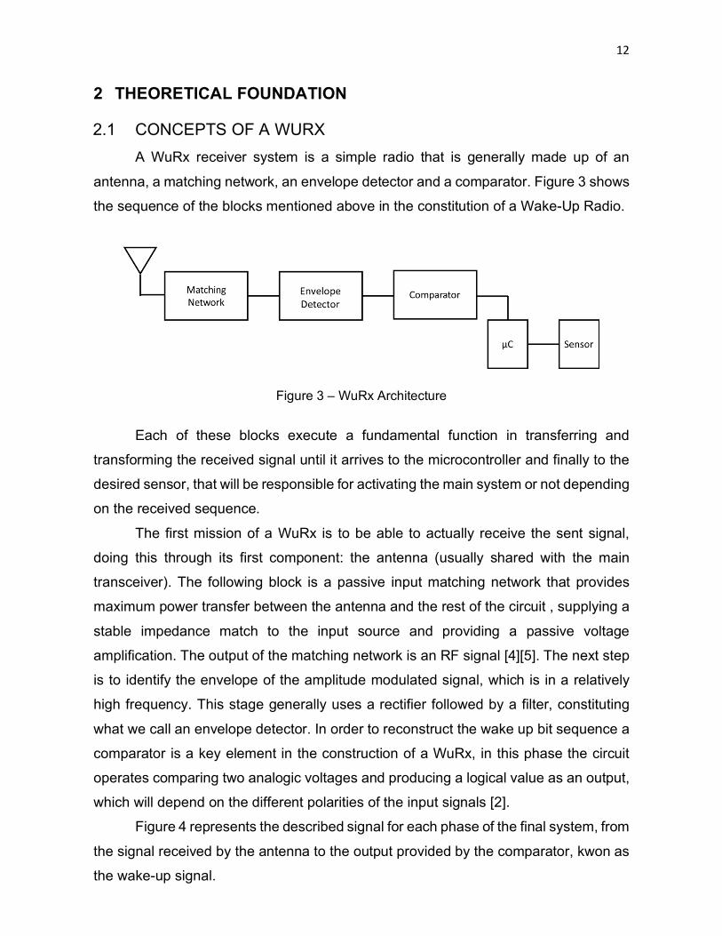
2.1 CONCEPTS OF A WURX A WuRx receiver system is a simple radio that is generally made up of an
antenna, a matching network, an envelope detector and a comparator. Figure 3 shows
the sequence of the blocks mentioned above in the constitution of a Wake-Up Radio.
Figure 3 – WuRx Architecture
Each of these blocks execute a fundamental function in transferring and
transforming the received signal until it arrives to the microcontroller and finally to the
desired sensor, that will be responsible for activating the main system or not depending
on the received sequence.
The first mission of a WuRx is to be able to actually receive the sent signal,
doing this through its first component: the antenna (usually shared with the main
transceiver). The following block is a passive input matching network that provides
maximum power transfer between the antenna and the rest of the circuit , supplying a
stable impedance match to the input source and providing a passive voltage
amplification. The output of the matching network is an RF signal [4][5]. The next step
is to identify the envelope of the amplitude modulated signal, which is in a relatively
high frequency. This stage generally uses a rectifier followed by a filter, constituting
what we call an envelope detector. In order to reconstruct the wake up bit sequence a
comparator is a key element in the construction of a WuRx, in this phase the circuit
operates comparing two analogic voltages and producing a logical value as an output,
which will depend on the different polarities of the input signals [2].
Figure 4 represents the described signal for each phase of the final system, from
the signal received by the antenna to the output provided by the comparator, kwon as
the wake-up signal.

13
Figure 4 – Signal throughout a WuRx
The next section seeks to better describe each one of the components that build
this type of system and the studied and chosen topologies for each case.
2.2 CIRCUIT ARCHITECTURE This section aims to describe in detail the functions, functionalities and features
of each one of the building blocks constituting the wake-up radio system as a whole,
including the matching network to the comparator. This description is followed by the
depiction of the studied topologies and the justification of choice to be used in the
construction of the circuit later on. In this unit, the function of the block for the general
system is presented first, followed by the theoretical foundations of its operation and
then the adaptation to the requirements of the project. The elements are presented in
the order in which they are applied for the constitution of the system.
2.2.1 Matching network
The impedance matching network is the block in charge of assuring the
maximum transfer of power between the antenna and the rest of the circuit, through
impedance matching in the input source. Typically, this network is made up of a LC
filter, in which the values of the inductor and the capacitor are dimensioned according
to the transmission frequency. The output of the block is a radiofrequency (RF) signal
that will connect to the envelope detector, responsible for retrieving the content of the
information from the modulated signal. Figure 5 is a schematic for a LC filter that can
be applied as a matching network.

14
Figure 5 – LC filter applied as matching network
Due to the size of the inductor and the capacitor, according to the used
references, this is usually a passive off chip circuit, since its total area would make it
unviable to be made as an integrated circuit.
2.2.2 Envelope detector
The goal of an envelope detector circuit is to capture an amplitude modulated
signal with a relatively high frequency and provide as an output the envelope of the
original signal. The base of this type of circuit is a rectifier, responsible for the
conversion of the alternated current input in a continuous pulsed signal, to which a filter
is added in order to smoothen the final result. Figure 6 depicts the expected signal to
be obtained for this type of circuit.
Figure 6 – Expected output signal for an envelope detector
In the case of this project, the chosen base was a voltage multiplier, as shown
on figure 7.

15
Figure 7 – Passive voltage multiplier
The voltage multiplier is a type of rectifier circuit using diodes to produce an
output voltage superior to the applied input voltage, according to the following formula:
𝑉#$% = 2𝑁(𝑉*+ − 𝑉-) (1) In which N represents the number of stages used and Vd is the threshold voltage
of the diodes.
In order to make an active version of the rectifier, the diodes can be substituted
by diode-connected transistors, as shown on figure 8.
Figure 8 – Active voltage multiplier
In this case, the formula becomes:
𝑉#$% = 2𝑁(𝑉*+ − 𝑉%/) (2) And Vth is the transistor’s threshold voltage.
Analyzing this condition, it is possible to conclude that this topology becomes
very limited for low voltage inputs [6]. An alternative to get around this limitation is a
cross coupled rectifier [7]. In this case, a polarization scheme is used in order to
increase the commutation transistors gate voltage in the rectifier. The proposed circuit
is as shown on figure 9.

16
Figure 9 – Cross-coupled rectifier
Using this topology, the output voltage is defined by the following equation:
𝑉#$% = 𝑁(2𝑉*+ − 𝑉%/) (3) For any of the two proposed topologies, it is possible to use several stages to
achieve higher output voltages. It is important to use an envelope detector topology
that assures the desired sensitivity.
In order for the circuit to work properly as an envelope detector, a high
impedance charge must be used in the output so that the recovery phenomenon
amplifies the signal level.
2.2.3 Comparator
Once the signal is rectified, the received wake up bit sequence is reconstructed
with the help of an comparator.
The comparator in a key element in analog to digital conversion. In general, it
operates comparing two analogic voltages (Vin and Vref) and producing a logical value
as an output, which will depend on the different polarities of the input signals. In the
example shown below for a traditional comparator, when our input voltage (Vin) is
smaller than the reference voltage (Vref), we have an output logic value “0”, when Vin
is greater than the reference voltage, our output is a logic value “1”. This operation is
shown in figure 10.
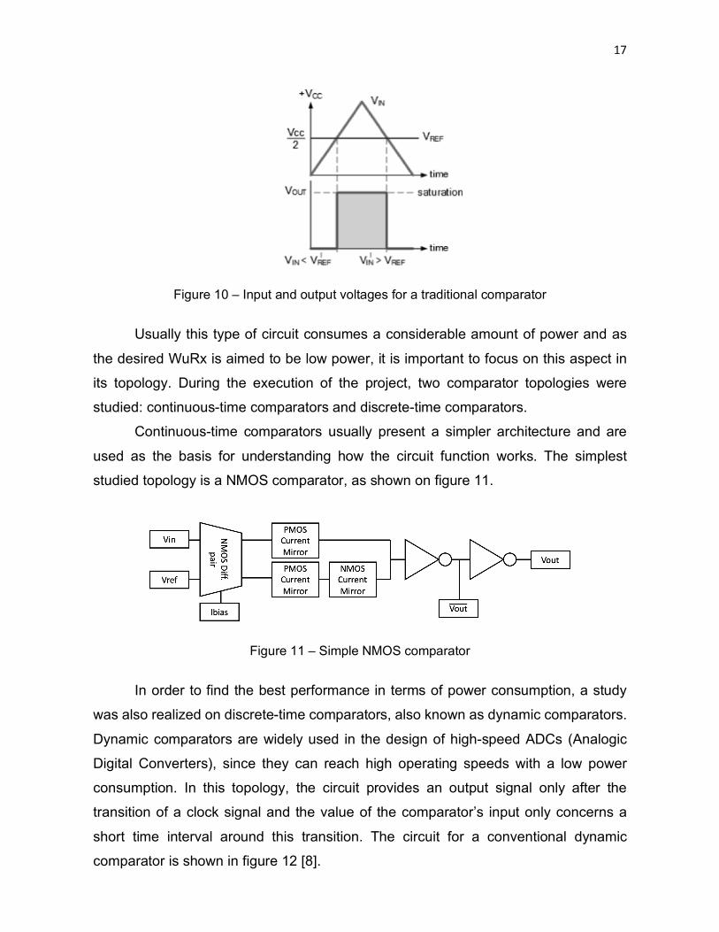
17
Figure 10 – Input and output voltages for a traditional comparator
Usually this type of circuit consumes a considerable amount of power and as
the desired WuRx is aimed to be low power, it is important to focus on this aspect in
its topology. During the execution of the project, two comparator topologies were
studied: continuous-time comparators and discrete-time comparators.
Continuous-time comparators usually present a simpler architecture and are
used as the basis for understanding how the circuit function works. The simplest
studied topology is a NMOS comparator, as shown on figure 11.
Figure 11 – Simple NMOS comparator
In order to find the best performance in terms of power consumption, a study
was also realized on discrete-time comparators, also known as dynamic comparators.
Dynamic comparators are widely used in the design of high-speed ADCs (Analogic
Digital Converters), since they can reach high operating speeds with a low power
consumption. In this topology, the circuit provides an output signal only after the
transition of a clock signal and the value of the comparator’s input only concerns a
short time interval around this transition. The circuit for a conventional dynamic
comparator is shown in figure 12 [8].

18
Figure 12 – Dynamic comparator
Several improvements can be made to this comparator topology, such as the
use of two tailed transistors to reduce power consumption and delays, optimize
structure to reduce offset voltage, and achieve greater precision of operation [9].
The studied dynamic comparator is composed by two stages: an interface stage
made up of all transistors except two cross-coupled inverters and a regeneration stage
that includes the two cross-coupled inverters, where each input is connected to the
output of the other. Each stage is responsible for one of the two operating stages of
the circuit. We also have a tail transistor connected to ground. When the clock is low,
the transistor is turned off and, depending on the input voltages, the output reaches
Vdd or Gnd. When the clock is high, the transistor is on and both outputs are discharging
to ground. The output voltages, which had been pre-charged on Vdd, begin to discharge
with different discharge rates depending on the corresponding input voltage. This
process is better detailed in the example below.
Considering the following input voltages for the circuit presented on figure 12:
• A clock signal;
• A pulse signal representing our bit sequence as the positive input
voltage;
• A constant voltage as the negative input voltage.

19
Figure 13 – Input voltages for the dynamic comparator
During the reset phase when CLK = 0 and Mtail is off, reset transistors (M7–M8)
pull both output nodes Outn and Outp to VDD to define a start condition and to have a
valid logical level during reset, as exemplified on figure 14.
Figure 14 – Dynamic comparator reset phase
In the comparison phase, when CLK = VDD, transistors M7 and M8 are off, and
Mtail is on. Output voltages (Outp, Outn), which had been pre-charged to VDD, start
to discharge with different discharging rates depending on the corresponding input
voltage (INN/INP). Assuming the case where VINP >VINN, Outp discharges faster than
Outn, if VINP< VINN Outn discharges faster than Outp. This is shown on figure 15.

20
Figure 15 – Dynamic comparator comparaison phase
According the operation detailed above, the output signals obtained are
depicted in figure 16.
Figure 16 – Output signals obtained for the dynamic comparator

21
2.3 CIRCUIT BENCHMARK
2.3.1 COTS circuit
As a base and in order to understand the general functioning of the system to
be developed, a characterization of a Wake-up radio consisting of the same functions
proposed on a PCB board with components off the shelf was carried out. The complete
circuit has the function of measuring and transmitting data concerning the room
temperature.
The analyzed circuit uses as a four-stage rectifier voltage multiplier with HSMS-
285C Schottky diodes and a TS811 integrated circuit as comparator to do the
demodulation [1].
As a first step, a communication test was made for the whole system using a
Manchester type signal at a frequency of 935 MHz. Since the receiver circuit uses
wireless power, it needs to charge the capacitors up to a supply voltage of 4 V before
the circuit starts to operate properly. In addition, the chosen rectifier has an efficiency
of 30% due to the chosen diodes. For a distance of about 1m in between the receiver
and transmitter, the result as showed on figure 17 was obtained by measuring the
signals of the receiver circuit.
Figure 17 - Measurements setup

22
Figure 18 - Signals measured for the COTS circuit
In figure 18 we have:
• Channel 1 (yellow): comparator input;
• Channel 2 (pink): comparator output;
• Channel 3 (blue): WuRx output;
• Channel 4 (green): microcontroller test output.
We verify with this test that the WuRx signal fulfills its function of waking up the
microcontroller for the reception of data. We can notice that following the reception of
the wake-up signal, the data received by the microcontroller is displayed (CH 4).
Following this test, the magnitude of the true voltage at the comparator input
and the sensitivity of the circuit for the four-stage rectifier and comparator were
measured. For a data rate of 1 kHz, an amplitude of 100 mV was measured at a
−30 dBm sensitivity, considering an input impedance of 50 W, and 10 mV at −40 dBm,
for the same condition. For the COTS circuit, the comparator is responsible for a
consumption of 780 nW.
These results were used to compare the performance of the circuit developed
during the project to the performance described in the used references.
2.3.2 State of the art references
In [10] the system consisted of an off-chip impedance matching network with a
large passive gain, an active envelope detector with a large input impedance and gain
and a low power precision comparator. The combination of the impedance network
with a high Q-factor and an envelope detector circuit with a large input impedance
enabled a passive voltage gain of 25 dB in the stage before the rectifier circuit. The
measured sensitivity for the circuit was −69 dBm, equivalent to 112.2 μV. With a Q-
factor of 25 and a voltage of about 30 mVp-p at the input of the envelope detector. The
total consumption for this circuit is 4.5 nW.

23
In the case of [11], the system also consists of an off-chip impedance matching
network, but this time, the Q-factor is close to 1. The voltage gain is obtained through
a 30 stage rectifier circuit and a dynamic comparator. The measured sensitivity for the
circuit was -40 dBm, equivalent to 3.16 mV. With a Q-factor of 1, and a gain of 30 for
the rectifier, a voltage of 100 mVp-p is obtained at the input of the comparator. For the
comparator circuit, we have a gain of 5 times, and a voltage of 500 mVp-p as output.
The total consumption of the circuit is 116 nW.
The following table synthesizes the most relevant values obtained in state-of-
the-art articles and the characterized COTS circuit.
Table 1 : Comparison between state of the art references
2.4 SPECIFICATIONS Having in mind the motivation of the project and the perspectives obtained
through the provided references, the specification presents the characteristics to be
applied and the objectives to be obtained throughout the project.
Other than the low power already mentioned in the previous paragraphs, other
issues must be considered, such as the sensitivity and the accuracy of the selective
awakenings.
Regarding the sensitivity, it is the characteristic that defines the smallest
correctly detectable signal. This value impacts the overall power consumption of the
radio and its range. The higher the sensitivity, the smaller the signals that can be
detected by the radio and the farther it can communicate. In order to improve
sensitivity, the system requires good amplification and noise performance.
Work Frequency (MHz)
Sensitivity (dBm)
Power consumption
(nW) Year
[4] 868 -55 1276 2015 [6] 868 -55 196 2014 [7] 868 -33 0* 2014 [10] 113.5 -69 4.5 2018 [11] 2400 -43.2 116 2015 [12] 405 -63.8 4.5 2017
COTS 935 -30 780 2018 *Fully passive with energy harvesting

24
Another issue that need to be addressed are false wake-ups, guaranteeing that
the system is precise in its selective awakenings. This is most commonly done with
CDMA codes that reject interferers and enable individual WuRx awakenings in the
presence of multiple similar systems.
These values were mainly defined using the possibilities found on the studied
references and in order to obtain improved results in terms of power consumption in
comparison to the characterized COTS circuit, while maintaining the same system
characteristics.
Characteristics of the Wake-Up Radio system.
• Frequency: 900 MHz
• Modulation: OOK
Objectives:
• Ultra-low power consumption: <100 nW – measured for the comparator;
• Modulation: high sensitivity: -35 dBm – measured for the envelope detector;
• Precise selective awakenings.

25
3 MATERIALS AND METHODS The materials used for the development of this project were as follows:
• Microsoft Excel: used for the calculations in order to characterize and scale
the different circuits and to calculate certain results;
• Cadence Virtuoso: used for the design and simulation of the circuits, as well
as the construction and verification of the layouts and post-layout simulation;
• IBM library for IBM130 nm RFCMOS technology: used on Cadence Virtuoso;
• Books, e-books and articles: used for theoretical foundation and definition of
operational parameters of the circuits making up the project.
The articles used as a comparison to the developed project were chosen
according to the following aspects:
• Active wake-up radio system containing an impedance matching network,
an envelope detector and a comparator as building blocks;
• Low power circuit;
• High sensitivity at envelope detector input.
The flowchart in figure 19 presents the simplified method used to develop the
Wake Up radio, including all the necessary circuits and integrations.

26
Figure 19 – Flowchart of the development of the Wake-Up Radio
From the parameter definition phase to the defined circuit for layout
construction, the necessary circuits were defined in the following order:
-Comparator;
-Rectifier, later on adapted to become an envelope detector.
Definition of the circuit’s main parameters
Circuit design
Circuit simulation
ok?
Circuit defined for layout
Layout construction
Layout validation
ok?
Post-layout simulation
ok?
Final circuit and layouts
yes
yes
yes
no
no
no

27
This order was chosen on terms of circuit complexity defined during the study
phase of the project, starting with the most complex circuit with multiple possibilities of
topology to the least complex.
The table in appendix 1 presents the action plan followed for the different stages
of the project as well as the necessary materials and methods and the objectives to be
attained.

28
4 DEVELOPMENT
4.1 CIRCUIT DESIGN Using the topologies previously studied, different alternatives of envelope
detector and comparator were developed and tested on Cadence Virtuoso, at a
transistor level. For each assembled circuit, in addition to the proper functioning of the
desired function, key characteristics have been tested and optimized in order to comply
with the specifications proposed for the project.
4.1.1 Matching network
As it is a simple circuit, with restricted topology alternatives and components
that would occupy a great area, the matching network is considered as an off-chip
circuit [1].
The values used for the capacitor and inductor were calculated according to the
desired frequency, established for the COTS circuit. The results obtained in its
measurements were later modeled to be considered as the inputs of the integrated
circuit for the envelope detector.
4.1.2 Envelope detector
For the envelope detector, the two studied circuits, voltage multiplier and cross-
coupled rectifier, were assembled on Cadence and their performances were
compared. The initial values of the components used in the circuit were based on
references with characteristics close to those desired and modified empirically to fine
tune the results.
The circuits as built on the software are shown in figures 20 and 21 and the
values for each component are specified on tables 2 and 3.

29
Figure 20 – Voltage multiplier rectifier
Table 2: Voltage multiplier rectifier parameters Parameter Value Unity
Cin 10 pF
M1, M2 W=5, L=0,60 µm
Figure 21 – Cross-coupled rectifier
Table 3: Cross-coupled rectifier parameters Parameter Value Unity
Cin 10 pF
M1, M2, M3, M4 W=5, L=0,60 µm

30
First, simulations were done to test the operation in rectifying mode. A PSS
simulation is used to visualize the operation of circuits in an input voltage range
(between 0 and 400 mV). The results of the PSS simulation for the cross-coupled
rectifier circuit and the voltage multiplier circuit are shown in Figures 22 and 23. The
images compare the results of the single and three stage circuits.
Figure 22 - Single-stage cross-coupled rectifier and voltage multiplier operation
Figure 23 - Three-stage cross-coupled rectifier and voltage multiplier operation

31
It is observed that for an input voltage higher than the threshold voltage of the
transistors (which is close to 350 mV for the chosen technology), the two circuits work
well according to the theory and we have for the cross-coupled rectifier a rectification
close to N (2Vin - Vth), greater than the rectification of the voltage multiplier, which is
2N (Vin - Vth). This result is observed for input voltages greater than 250 mV. For an
input voltage between 100 mV and 200 mV, therefore below the threshold voltage of
the transistors, the circuit rectifies the signal but the value of the output voltage is not
easily calculable.
Looking at the results of the simulations, we can conclude that for these values
of input voltage, the cross-coupled rectifier has a better performance than the voltage
multiplier. If we increase the number of stages in the circuits, we continue to increase
the rectified voltage but the increase does not occur linearly, as expected in theory.
For an input voltage lower than 50 mV, well below the threshold voltage of the
transistor, we still have a rectification, but the output voltage does not increase with
increasing stages. Using this voltage level, the transistor stops working and
rectification comes mostly from the first local PN junction the signal finds than from the
circuit topology.
In order to use circuits in envelope detector mode, a high impedance output load
must be used. In this case, the choice was a resistance of 1 GΩ and a capacitance of
50 fF, values which allow a suitable conversion factor.
To simulate an operation close to the WuRx system, an OOK signal is generated
on Cadence Virtuoso using a pvcvsp source to combine a vbits source and a sinusoidal
source, as shown on figure 24. The Vin pin is directly connected to the input of the
rectifier circuit.
Figure 24 – OOK signal simulation on Cadence Virtuoso

32
According to the specifications, the frequency of the signal generated by the
sinusoidal source was 900 MHz. Transient simulations were made with a 50 mV
amplitude Vin signal for the single-stage voltage multiplier circuit and for the single-
stage cross-coupled circuit as well. The results obtained are shown in Figures 25 and
26, respectively.
Figure 25 - Single-stage voltage multiplier envelope detector operation
Figure 26 – Single-stage cross-coupled rectifier envelope detector operation

33
According to the results obtained, since we aim to work at low input voltages,
the best option found is to use only one stage of the cross-coupled rectifier circuit,
since we have a much cleaner curve for this topology.
4.1.3 Comparator
First to test the operation of a comparator circuit and better understand its
principles, the simple topology of a NMOS comparator was assembled on Cadence.
The circuit as built in the software is shown in figure 27 and the values of each
component are specified on table 4.
Figure 27 - Simple NMOS comparator
Table 4: Simple NMOS comparator parameters Parameter Value Unity
M1, M3, W=0,500, L=0,180 µm
M2, M4 W=0,500, L=0,210 µm
M5 W=0,320, L=0,290 µm
M6 W=0,380, L=0,370 µm
M7,M8 W=0,600, L=0,180 µm
M9 W=0,600, L=0,190 µm
M10 W=0,600, L=0,260 µm
M11, M13 W=1,200, L=0,180 µm
M12, M14 W=0,600, L=0,180 µm

34
To test the operation of the circuit, a triangular wave was applied to one of the
differential inputs and a reference voltage with the mean value of the triangular wave
was applied to the other entry. The result obtained by doing a transient simulation is
as seen in figure 28.
Figure 28 - Simple NMOS comparator operation
Despite the good functioning of the comparator circuit, by reducing the supply
voltage value in order to reduce the consumption, for values lower than 1 V, we start
to have a significant delay between the input and the output generated by the circuit.
The lowest power consumption obtained for this circuit was 2.5 μW, with an input
voltage of 1 V. Since this consumption is higher than the one presented by the COTS
circuit, other circuits were studied and tested to try to optimize this parameter, which is
essential to the success of the project.
From the studied benchmarks, a good option for a low power comparator is the
Dynamic Latch Comparator which has had its operation explained in the previous
sections.
For this topology, two circuits were assembled and tested on Cadence, the
reference circuit with the lowest consumption and the reference circuit with the best
overall performance according to [9]. Both arrangements can be seen in Figures 29

35
and 30 and the values used for the components in each case are specified on tables
5 and 6.
Figure 29 – Dynamic Latch comparator 1
Table 5: Dynamic latch comparator 1 parameters Parameter Value Unity
M1, M2, M3, M4, M11, M12 W=1,040, L=0,180 µm
M5, M6, M7, M8, M9, M10,
M13, M14, M15 W=0,520, L=0,180 µm

36
Figure 30 – Dynamic Latch comparator 2
Table 6: Dynamic latch comparator 2 parameters Parameter Value Unity
M1, M2, M3, M4, M5, M6,
M11, M12, M13, M14, M20,
M22
W=1,040, L=0,180 µm
M7, M8, M9, M10, M15, M16,
M17, M18, M19, M21, M23 W=0,520, L=0,180 µm
As for the NMOS comparator, the two circuits were simulated in transient mode.
Initially, two rectangular signals were used at the inputs. The result obtained for each
circuit was as expected for a comparator, with an interface stage and a regeneration
stage, as previously explained on section 3.2.2.
To measure the power consumption of the circuits, which was a challenge at
this stage, as there were peaks at each clock transition and data, the curve of the
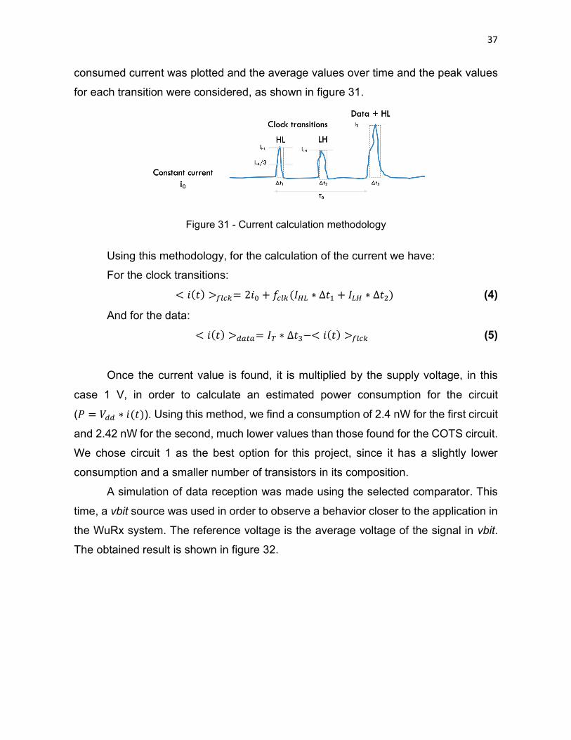
37
consumed current was plotted and the average values over time and the peak values
for each transition were considered, as shown in figure 31.
Figure 31 - Current calculation methodology
Using this methodology, for the calculation of the current we have:
For the clock transitions:
< 𝑖(𝑡) >4567= 2𝑖8 + 𝑓657(𝐼<= ∗ ∆𝑡@ + 𝐼=< ∗ ∆𝑡A) (4)
And for the data:
< 𝑖(𝑡) >-B%B= 𝐼C ∗ ∆𝑡D−< 𝑖(𝑡) >4567 (5)
Once the current value is found, it is multiplied by the supply voltage, in this
case 1 V, in order to calculate an estimated power consumption for the circuit
(𝑃 = 𝑉-- ∗ 𝑖(𝑡)). Using this method, we find a consumption of 2.4 nW for the first circuit
and 2.42 nW for the second, much lower values than those found for the COTS circuit.
We chose circuit 1 as the best option for this project, since it has a slightly lower
consumption and a smaller number of transistors in its composition.
A simulation of data reception was made using the selected comparator. This
time, a vbit source was used in order to observe a behavior closer to the application in
the WuRx system. The reference voltage is the average voltage of the signal in vbit.
The obtained result is shown in figure 32.

38
Figure 32 - Dynamic Latch Comparator 1 operation
We observe that when we have “1” at the input (high level of the signal
generated by the vbit source), we have a low level signal at the positive output. On the
other hand, if we have “0” at the input (low level of the signal generated by the vbit
source), we have a low level signal at the negative output. To have a good functioning
of the circuit, it was found that the clock frequency must be at least five times greater
than the frequency of generation of bits, this was determined empirically.
4.2 SUGGESTED CIRCUIT LAYOUT The proposed layouts were built according to the method presented in section
3, for each of the final circuits chosen previously. Several layout optimization
techniques were applied, such as: previous floor planning, device matching and
orientation, common centroid and symmetry [13].
4.2.1 Envelope detector Layout
For the envelope detector circuit, as mentioned previously, the chosen topology
was a cross coupled envelope detector, composed of 2 capacitors and 4 transistors.
As the capacitors occupy the main area of the integrated circuit, the transistors were
positioned between these two components in order to optimize the space. The inputs

39
of the circuit are located on the top of each capacitor, while the output is located on the
right top area of the transistors and the reference on the left bottom area, since it is
usually connected to gnd. The final area of the proposed circuit is constituted by a
height of 96.19 µm and a length of 52.28 µm.
Figure 33 shows the suggested layout as a whole.
Figure 33 – Envelope detector layout
The detail of the envelope detector layout, highlighting the central devices is
shown in figure 34.
Figure 34 – Zoom of the envelope detector layout

40
4.2.2 Comparator Layout
Concerning the comparator, the chosen topology was the one that presented
the lowest power consumption, the first model of the dynamic latch comparator, made
up of 15 transistors. For this layout, each block of the final comparator was built
individually to be later assembled into the final circuit. The inputs are strategically
placed on the left, the outputs on the right and the clock signal on the lower part of the
circuit, as defined on the previous floorplan. The final area of the proposed circuit is
constituted by a height of 17.70 µm and a length of 38.43 µm.
Figure 35 shows the suggested layout
Figure 35 – Comparator Layout

41
5 RESULTS The main results obtained from the simulations for the desired characteristics,
already presented in the corresponding development sections, are synthesized in
tables 7 and 8 for each of the built circuits.
Table 7: Envelope detector specification
Parameter Value Unity Input voltage 50 mVp-p
Area 96.19 x 52.28 µm2
Operating temperature 27 °C
Table 8: Comparator specification
Parameter Value Unity Supply voltage 1 V
Calculated Current 2.4 nA
Power consumption 2.4 nW
Area 17.70 x 38.43 µm2
Operating temperature 27 °C
Considering that the initial objectives of the project :
• Ultra-low power consumption: <100 nW – measured for the comparator;
• High sensitivity: -35 dBm – measured for the envelope detector.
The power consumption considered for this purpose was the one obtained for
the comparator circuit, which according to the studied references, is usually the main
power consumer of the WuRx system. For the developed project, the value obtained
for this aspect was 2.4 nW. A huge improvement compared to the characterized COTS
circuit, which presents a value of 780 nW for this same parameter.
Regarding the sensitivity, in this case, this is an aspect mainly defined by the
operation of the envelope detector, which in this developed project was capable of
operating with an input voltage of 50 mVp-p. Since for this work, we are considering the
characteristics of the matching network of the COTS circuit to model the input of our
system, this implies on a Q-factor of approximately 4, which gives us an input voltage
of 12,5 mVp-p at the input of the WuRx, equivalent to -34 dBm, considering an

42
impedance of 50 W. This result is very close to the established objective of -35 dBm
and represents an improvement regarding the COTS circuit, which presented a
measured sensitivity of -30 dBm.
Figure 36 compares in a visual manner the values obtained in the simulations
of the transistor level circuit developed during the project and the values of the
characterized COTS circuit previously explained.
Figure 36 - Circuit measurements comparison
In short, considering the obtained results, the projected circuit was able to
improve the desired characterized values, obtaining through the low-power dynamic
comparator a much reduced power consumption of 2.4 nW and through the envelope
detector a higher sensitivity, functioning at 50 mVp-p. The values in the input of the
system were estimated based on the performance of the matching network of the
COTS circuit in both cases and represent a sensitivity of -34 dBm for the proposed
project.
These results were later compared to the benchmark values defined in the
study phase of the project. Table 9 synthesizes the values found on the references
and in the last line, the results of this project.

43
Table 9 : Comparison between this work and the studied references
In comparison to the other works presented as references, the proposed circuit
has a very low power consumption, while the sensitivity can still be improved.
In the studied works, some modifications are already identified in order to better
tune the built circuits, such as:
• Switched-capacitors as comparator inputs to combat kickback
noise;
• Use of two tail transistors on the comparator to reduce power
consumption and delays;
• Comparator structure optimization to reduce offset voltage.
In addition, other topologies of the envelope detector can be studied or else the
use of transistors with a technology presenting a lower threshold voltage, in order to
obtain a circuit that works with even lower input voltages.
Work Frequency (MHz)
Sensitivity (dBm)
Power consumption (nW) Year
[4] 868 -55 1276 2015 [6] 868 -55 196 2014 [7] 868 -33 0* 2014
[10] 113.5 -69 4.5 2018 [11] 2400 -43.2 116 2015 [12] 405 -63.8 4.5 2017
COTS 935 -30 780 2018 This work 900 -34 2.4 2020
*Fully passive with energy harvesting

44
6 MARKET POTENTIAL Bearing in mind that this type of system is used in networks of communicating
objects and the great growth of this type of application in the last years and in the years
to follow, this section aims to briefly explore the market potential of the developed
project.
Since basically everything can be connected to the Internet, there is seemingly
no upper limit to the growth potential for the application on communicating objects, a
market more commonly known as Internet of Things. According to a report published
by the Mckinsey Global Institute in 2016 [14], the IoT market will grow to somewhere
between 3.9 to 11.1 trillion USD by 2025, being equivalent at least to the current GPD
of Germany. The top two application areas are predicted to be Health Care and
Manufacturing, a forecast also made by the market research company Gartner [15].
As in 2020 worldwide IoT spending surpassed 1 trillion USD, and just three industries:
discrete manufacturing, logistics and transportation, and utilities have accounted
for 50% of all IoT spending.
While IoT devices may vary in application and come in different forms and
manners, in general they will require common functioning blocks enabled by analog
electronics. IoT applications cannot work without sensors and integrated circuits, so all
IoT devices will require semiconductors. This industry is broadly reshaped by the
market requirements aiming to increase the number of device used at the same time,
while guaranteeing a reliable connection and keeping the users and the data safe. In
order to do so, wireless communication systems must focus on a certain number of
elements, such as design for power and precision, both target characteristics of the
presented project.
The proposed circuit is an essential building block in order to maintain sensor
networks working in a low power routine, and can be used for the most various
applications throughout the communicating objects industry, being a base block for
autonomous systems, such as those used in smart cities, home automation and self-
driving vehicles, trends presented only as illustrations of the countless possibilities. In
a world of machine-machine interactions, a sensor system is essential for the
perception of the surrounding environment, providing the basic data for the operation
of a later automation.

45
7 CONCLUSION AND FUTURE WORK At the end of the proposed project, the expected functioning and the desired
characteristics according to the specifications defined before the project execution
were achieved. In a manner that the specific objectives of designing the envelope
detector and the comparator, as well as their layouts, in addition to the step of
comparing results with other works and the characterized COTS circuit, were all
completed.
This project has led to a better understanding of the function and operation of a
Wake-Up radio system and its building blocks. In addition, different envelope detector
and comparator circuits were investigated, as well as optimization techniques to
achieve better accuracy and lower power consumption for the WuRx.
At a software level, the project also provided training for new simulations in the
Cadence Virtuoso environment. It can be concluded that the project was a great
learning curve in the field of analog electronics, going through several circuit design
processes.
For future projects, the main optimizations can be done throughout the
comparator, aiming to decrease the circuit’s power consumption and increase the
sensitivity, as well as the modification of the circuit to work with more complex
modulations. The next steps would involve the union of the circuits and tests including
the matching network, followed by the application of the whole system connected to a
microcontroller, executing the full function proposed by the COTS circuit.

46
8 REFERENCES
[1] NICOT John, FADEL Ludivine, TARIS Thierry, 2019,”An RF-Powered IoT Node
for Environment Sensoring”.
[2] ROBERTS Nathan E. et WENTZLOFF David D., 2015, ”Ultra-Low Power Wake-
Up Radios”.
[3] Statista Research Department, 2017, “Internet of Things (IoT) connected devices
installed base worldwide from 2015 to 2025”.
[https://www.statista.com/statistics/471264/iot-number-of-connected-devices-
worldwide/]
[4] SPENZA Dora, MAGNO Michele, BASAGNI Stefano, BENINI Luca, PAOLI Mario,
PETRIOLO Chiara, “Beyond Duty Cycling: Wake-up Radio with Selective
Awakenings for Long-lived Wireless Sensing Systems”.
[5] CHENG Kuang-Wei , LIU Xiu, JE Minkyu, 2012, "A 2.4/5.8 GHz 10 μW Wake-Up Receiver With -65/-50 dBm Sensitivity Using Direct Active RF Detection”
[6] MAGNO Michele, BENINI Luca, 2014,”An Ultra Low Power High Sensitivity Wake-
Up Radio Receiver with Addressing Capability”.
[7] KAMALINEJAD Pouya, KEIKHOSRAVYL Kamyar, MAGNO Michele, MIRABBA-
SIL Shahriar, LEUNG Victor C.M., BENIN Luca, 2014, ”A High-Sensitivity Fully
Passive Wake-Up Radio Front-End for Wireless Sensor Nodes”.
[8] SATHISHKUMAR A. et SARAVANAN S., 2014, ”Analysis and Design of Low
Power High Speed Dynamic Latch Comparator using CMOS Process”.
[9] SAROJAL G. et SATYANARAYANA M., 2016, ”Design Of High Performance
CMOS Dynamic Latch Comparator”.
[10] WANG Po-Han Peter, JIANG Haowei, GAO Li, SEN Pinar, KIM Young-Han, RE-
BEIZ Gabriel M., MERCIER Patrick P., HALL, Drew A., 2018, ”A Near-Zero-Power
Wake-Up Receiver Achieving −69-dBm Sensitivity”.

47
[11] OH Seunghyun,ROBERTS Nathan E. et WENTZLOFF David D., 2013, ”A
116nW Multi-Band Wake-Up Receiver with 31- bit Correlator and Interference
Rejection”.
[12] WANG Po-Han Peter, JIANG Haowei, GAO Li, SEN Pinar, KIM Young-Han, RE-
BEIZ Gabriel M., MERCIER Patrick P., HALL, Drew A., 2017, “A 400 MHz 4.5 nW
−63.8 dBm Sensitivity Wake-up Receiver Employing an Active Pseudo-Balun
Envelope Detector”.
[13] SAINT Christopher, SAINT Judy, 2004, “Ic Mask Design: Essential Layout
Techniques”
[14] Mckinsey & Company, 2016, “Unlocking the potential of the Internet of Things”.
[http://www.mckinsey.com/insights/business_technology/the_internet_of_things_the_
value_of_digitizing_the_physical_world]
[15] Gartner, 2016, “Gartner Says the Internet of Things Installed Base Will Grow to
26 Billion Units By 2020”. [https://www.gartner.com/newsroom/id/2636073]

48
9 APPENDIX
9.1 APPENDIX 1
Table : Materials and methods used to carry out the project tasks.
Task Material Method Objective
Researches concerning comparator topologies
Articles
Researches on low power comparator on IEEE Explore portal
Find the optimal comparator topology for the project descriptions
Assembly of the comparator circuit
Cadence virtuoso
Schematic assembly
Assemble the comparator circuit
Comparator circuit simulation
Cadence virtuoso
Transient simulation with triangular signal
Check if the circuit is working according to the expected function
Comparator circuit simulation
Cadence virtuoso
Transient simulation with bit signal
Current measurement to calculate power consumption
Calculation of comparator power consumption
Excel
Use of current values obtained in the transient simulation
Calculate the circuit’s power consumption
Researches concerning envelope detector topologies
Articles
Researches on sensible envelope detector on IEEE Explore portal
Find the optimal envelope detector topology for the project descriptions
Assembly of the one stage rectifier circuit
Cadence Virtuoso
Schematic assembly
Assemble the rectifier circuit
One stage rectifier circuit simulation
Cadence Virtuoso PSS simulation Define the rectifier
voltage gain Assembly of the three-stage rectifier circuit
Cadence Virtuoso
Schematic assembly
Assemble the rectifier circuit
Three stage rectifier circuit simulations
Cadence Virtuoso PSS simulation Define the rectifier
voltage gain
Assembly of the rectifier envelope detector
Cadence Virtuoso
Schematic assembly
Assemble the envelope detector circuit
Rectifier envelope detector circuit simulations
Cadence Virtuoso
Transient simulation with modulated signal
Check if the circuit is working according to the expected function

49
Assembly of the cross coupled rectifier circuit
Cadence Virtuoso
Schematic assembly
Assemble the cross coupled rectifier circuit
One stage cross coupled rectifier circuit simulation
Cadence Virtuoso PSS simulation Define the rectifier
voltage gain
Assembly of the three-stage cross coupled rectifier circuit
Cadence Virtuoso
Schematic assembly
Assemble the rectifier circuit
Three-stage cross coupled rectifier circuit simulations
Cadence Virtuoso PSS simulation Define the rectifier
voltage gain
Assembly of the cross coupled rectifier envelope detector
Cadence Virtuoso
Schematic assembly
Assemble the envelope detector circuit
Cross coupled rectifier envelope detector circuit simulations
Cadence Virtuoso
Transient simulation with modulated signal
Check if the circuit is working according to the expected function
Comparison of envelope detector topologies
Excel Use of results obtained in the simulation
Definition of the best envelope detector for the project
Comparator Layout Cadence Virtuoso
Use the circuit schematic to build the layout
Build the circuit layout
Comparator Layout checks
Cadence Virtuoso
DRC (Design Rule Check) LVS (Layout Versus Schematic) Parasite Extraction
Check if the layout rules have been followed and if the layout corresponds to the circuit built as a schematic
Post Layout simulation on Comparator Layout
Cadence Virtuoso
Transient simulation with modulated signal
Check if the layout circuit is working according to the expected function
Envelope detector Layout
Cadence Virtuoso
Use the circuit schematic to build the layout
Build the circuit layout
Envelope detector Layout checks
Cadence Virtuoso
DRC (Design Rule Check) LVS (Layout Versus Schematic) Parasite Extraction
Check if the layout rules have been followed and if the layout corresponds to the circuit built as a schematic
Post Layout simulation on Envelope detector Layout
Cadence Virtuoso
Transient simulation with modulated signal
Check if the layout circuit is working according to the expected function