Embed Size (px)
Citation preview
DESIGN OF A DSP-BASED SERVO SPEED CONTROLLER
by
Jiabing Lu, B. Eng
A thesis submitted to
Dublin City Universityfor the degree of
Master of Engineering
School of Electronic Engineering
DUBLIN CITY UNIVERSITY
July 1992
Abstract
The brushless servo drive is arguably the most important emerging drive category for
robotics, machine tools and other applications. This places increasingly high demands
on the servo motor and controller.
In this thesis, a digital speed and thermal protection controller is developed for a high
performance brushless DC servo system. The speed controller is designed to produce
a high accuracy and a fast dynamical response. The thermal protection controller
prevents the motor against overheating while providing a high utilization of the drive.
Two PID design methods are studied for the speed controller, an "analog design
approach" and a "grapho-analytical pole-placement procedure". The former provided an
easy design and the later resulted in a more satisfactory control performance.
The thermal protection controller uses a generic lumped capacitance-resistance thermal
model to predict the motor temperature. A current limit regulator is developed to
maintain the motor temperature below this insulation limit, and to maximize the motor
output once the limit is reached.
A simulation scheme for this servo system is developed to investigate the control
characteristics of the system before experimental testing.
The digital speed controller has been implemented using the TMS320C30, a high
performance digital signal processor. The control software, written in the TMS320C30
assembly language, is developed.
Experimental results are presented, which demonstrate the performance improvement of
the designed control system.

DECLARATION
I hereby declare that all the work presented in this thesis is my own, except
where references have been made. I also declare that no part of this thesis has been
submitted for a degree at any other institution.
0 ¿¿/¡i/if £**-SIGNATURE:_______________________
DATE:____________• H -

ACKNOWLEDGEMENTS
I wish to express my sincere gratitude to my supervisor, Dr. A. Murray, who provided
me the opportunity to undertake this research project for a higher degree. Throughout
the course of this work, he has been a constant source of advice, support and
encouragement, which is and will always be much appreciated.
I also wish to thank Dr. M.J. Barrett, J. Se ton and P. Moran for their help in proof
reading the thesis and helping to turn it into a readable document.
Thanks to all technical staffs of the school of Electronic Engineering, especially
C. Maguire, S. Neville, D. Condell and J . Whelan for providing the necessary
equipment and help to complete this research.
Thanks to my fellow postgrads in the power electronics laboratory for their kind help
and support.
Finally a special thanks to Dr. J . Yan for his valuable assistance and encouragement
during this research.
CONTENTS
CHAPTER 1 INTRODUCTION ..................................................................................1
CHAPTER 2 PERMANENT MAGNET BRUSHLESS DRIVE SYSTEM................. 5
2.1 Introduction..................................................................................................5
2.2 Brushless DC d riv e .......................................................................................6
2.2.1 The motor ..................................................................................... 6
2.2.2 The sensing sy stem ........................................................................6
2.2.3 The electronic commutator ..........................................................7
2.3 Mode of opera tion ........................................................................................7
2.3.1 The three-phase half-wave BLDC d riv e ......................................7
2.3.2 The three-phase full-wave BLDC d r iv e ..................................... 8
2.4 Brushless motor characteristics.............................................................. 12
2.5 Position sensing sy s te m .............................................................................14
2.6 Brushless motor servo c o n tro l ..................................................................14
CHAPTER 3 DESIGN OF THE DIGITAL SPEED CONTROLLER ............... 18
3.1 Introduction ................................................................................................18
3.2 The servo system m odel.............................................................................19
3.3 Simplifying the mathematical model ...................................................... 21
3.3.1 Current loop simplification ........................................................21
3.3.2 Filters and tachogenerator sim plification.............................. 23
3.3.3 The open-loop transfer function ........................................ 26
3.4 Analogue design of the discrete controller..............................................26
3.4.1 Minimum peak overshoot method ..........................................27
3.4.2 Optimizing model m ethod................................ 33
3.4.3 Discretization of the analogue con tro lle r.............................. 35
3.5 Design of a digital controller using the pole-placement technique . . . 38
3.5.1 Design requirements .................................................................. 38
3.5.2 Design speed digital con tro ller.................................................. 39
3.5.3 Selection of controller parameters............................................... 40
3.5.3.1 The selection of sampling interval ............................ 40
3.5.3.2 The characteristic equation of closed-loop system . 41
3.5.3.3 Graph-analytical m e th o d .............................................45
3.5.3.4 Parameter calculation..................................................48
3.6 Conclusion................................................................................................... 50
CHAPTER 4 SIMULATION OF BRUSHLESS SERVO SYSTEM ..........................51
4.1 Introduction.................................................................................................51
4.2 The typical b lo c k ........................................................................................ 53
4.2.1 Numerical integration method for the differential equation . 54
4.3 Block-oriented simulation program .......................................................... 55
4.3.1 Simulation of the continuous part of the system ...................... 55
4.3.2 Simulation of the digital controller............................................ 56
4.4 Simulation resu lts........................................................................................ 57
4.5 Conclusion................................................................................................... 58
CHAPTER 5 BRUSHLESS MOTOR THERMAL PROTECTION ........................ 60
5.1 Introduction.................................................................................................60
5.2 Power l o s s ................................................................................................... 61
5.2.1 Power flow of a brushless m otor...............................................62
5.2.2 Thermal power loss calculation................................................. 63
5.2.3 Maximum allowable power loss ...............................................64
5.2.4 Calculation the equivalent resistance Rj,.................................. 66
5.2.5 Drawing the max continuous Speed-torque c u rv e .................. 67
5.3 Single-component thermal model .............................................................69
5.3.1 Thermal resistance .................................................................... 69
5.3.2 Thermal capacitance ................................................................. 71
5.3.3 Thermal equation ....................................................................... 71
5.4 Two-component thermal model ................................................................73
5.4.1 Establishing thermal m o d e l .......................................................73
5.4.2 Winding temperature calculation.............................................. 73
5.5 Brushless motor thermal protection control procedure........................... 75
5.6 Thermal protection sim ulation.................................................................. 76
5.7 Conclusion................................................................................................... 78
CHAPTER 6 IMPLEMENTING THE TMS320C30 CONTROLLER................. 82
6.1 Introduction ................................................................................................ 82
6.2 The TMS320C30 PC system board description........................ 84
6.2.1 P rocessor..................................................................................... 84
6.2.2 Memory m a p ................................................................................85
6.2.2.1 Memory maps .............................................................85
6.2.2.2 Peripheral bus map ................................................. 85
6.2.2.3 Reset/interrupt/trap vector m a p .............................. 85
6.2.2.4 External memory map ............................................... 86
6.2.3 Analogue interface ..................................................................... 88
6.3 Software design ...........................................................................................89
6.3.1 Selection of software tools.......................................................... 89
6.3.2 Program flowchart ..................................................................... 89
6.3.2.1 Initializing rou tine ....................................................... 89
6.3.2.2 Control rou tine .............................................................99
6.4 PC control program .................................................................................102
6.5 Conclusion................................................................................................. 102
CHAPTER 7 PERFORMANCE MEASUREMENT................................................ 104
7.1 Introduction.............................................................................................. 104
7.2 Experimental equipment and procedure ................................................ 104
7.3 Test of the servo system .........................................................................105
7.3.1 Design I t e s t ..............................................................................105
7.3.2 Design II te s t ..............................................................................105
7.3 Sensitivity to controller param eters........................................................ 106
7.4 Conclusion................................................................................................. 106
CHAPTER 8 CONCLUSION AND RECOMMENDATION ................................113
8.1 Conclusions .............................................................................................. 113
8.2 recommendations...................................................................................... 115
8.2.1 Sinusoidal type of brushless AC m o to r...................................115
8.2.2 All-digital c o n tro l..................................................................... 115
8.2.3 More advanced control algorithms.......................................... 115
REFERENCE ...............................................................................................................117
i ii
APPENDIX A THE SERVO SYSTEM MODEL ............................................... Al
APPENDIX B ............................................................................................................. B1
B-I. The simulation program for design I .......................................................B1
B-II. The simulation program for design I I ....................................................B5
APPENDIX C ................................................................................................................Cl
C-l. The program for the Speed-Torque characteristics..................... Cl
C-2. Measurement of the BHT motor PWM power lo s s .............................. C3
C-3. The simulation program for the motor temperature............................... C4
APPENDIX D ............................................................................................................... D1
D-l. TMS320C30 assembly language program ........................................... D1
D-2. The PC control program ........................................................................ D7
D-3. Interface circuit design...........................................................................D9
D-3.1. Interface board using inverting amplifiers ...........................D9
D-3.2. Interface circuit .................................................................... D ll
iv
CHAPTER 1INTRODUCTION
Brushless dc motors with permanent magnetic material, such as Samarium-Cobalt, have
been in ever-increasing use for more than ten years. They are currently considered
among the best options not only in high performance control systems such as machine
tool feed drives, robotics, indexing equipment, punch/press machines, radar/antenna
drives, and tracking systems, but also in more mundane applications such as consumer
and commercial air conditioning, etc [1-1]. At present, modem methods , technology
and materials have enabled the industry to develop large (up to 200 hp) brushless dc
motors to operate as general purpose machines to do the routine tasks of variable speed
control in the industry applications such as pumps, conveyors, extruders, presses etc.
The permanent magnet brushless DC motor has the following major advantages:
(1) high starting torque;
(2) high torque at low speed;
(3) excellent speed regulation (greater than 20,000:1) from no load to full load;
(4) low inertia;
(5) easy maintenance;
(6) high power/volume ratios since the windings are only on the stator, therefore
the I2R thermal losses can be more easily dissipated in the air - this allows a
brushless motor of the same frame size as a brush motor to have a higher specific
power output;
(7) a high degree of accuracy of the adjustable speed or position;
(8) easy to control;
(9) capable of operating in clean and hazardous environments in industries such
as food processing, chemical and aeronautics industries or operating fully
immersed in fluid or vacuum;
(10) better overall efficiency because any friction losses between the brush and
the commutator are eliminated;
1
(11) a constant power factor, better than 90% even at zero speed, and typically
95 % when driven by a pulse width modulated motor drive.
The prices of brushless dc motors are becoming competitive than ever due to the
increasing market for these motors, the continual improvement in the manufacturing
process of the motors, and the advancements in the solid-state power electronic devices
and circuits. These brushless motors are replacing, at a rapid pace, the existing
hydraulic as well as the conventional electric drive systems in a number of applications
that require the above advantages.
At present most brushless dc drives are controlled using analogue controllers. However,
with the rapid development of microcomputers, especially the DSP processor, digital
feedback control is being now applied. The control results achieved through digital
control are often better than analogue systems and they are much less expensive to
implement, change or replace. Digital controllers can exchange complex blocks of
information at quite high speeds and can store different programs, some of which are
scheduled only if certain conditions are met. They are not affected by component aging
and temperature drift, and they enhance greatly the performance characteristics of the
system. At present, digital computers are much smaller, lighter and more powerful.
Their cost and their power requirements are reasonably low and becoming lower every
year. They are ideal control device for the servo application.
The aim of this thesis is to develop a digital speed controller for a permanent magnet
brushless DC servo motor that will replace the analogue speed loop of the system and
develop a thermal protection for the brushless dc motor. A digital signal processor,
TMS320C30, is used for this purpose.
This thesis presents two digital control methods used in the design of the speed
controller. An "analogue design of discrete controller" method [1-7] is successfully
achieved due to the high speed of the TMS320C30. This method combines the
advantages of fast sampling intervals of the TMS320C30 and well-developed analogue
design techniques. This makes the controller design become simple and convenient. An
2
alternate design of the speed controller is a direct-digital proportional-integral-derivative
implementation based on a pole-placement technique [1-8]. Using this scheme one can
obtain a desired performance by adjusting the control parameters on the accuracy, speed
of response, and stability margin of the system. This controller has a better dynamic
performance due to the fact that a more accurate direct digital design method than the
first designed controller is used.
A simulation method is also described in the thesis. The method using a block-oriented
technique exactly simulates the designed system on a personal computer. This can
examine the system and adjust the parameters of the controller to the desired level before
a practical test is carried out on the system. Implementations of the simulation are
presented.
The thermal protection of PM brushless motors is a key problem in motor servo drives
in industrial applications. This thesis presents a real-time thermal protection control
scheme for a brushless DC servo motor. A thermal model of the motor is established,
and the thermal controller uses this to predict the temperature of the motor windings.
Once the predicted temperature reaches the winding insulation limit, the thermal
controller maintains the motor operation within a maximum allowable speed-torque
region. This keeps the winding temperature below the insulation limit, while
maximizing the motor power output. Simulation results for this scheme are presented.
An implementation of the TMS320C30 based control system is detailed and a real-time
control software program is developed to realize this DSP based servo system. The
experimental results are presented and this shows the successful design of the digital
speed controller for the brushless DC drive system using the TMS320C30 DSP device.
Thesis Structure
The thesis is divided into eight chapters. Chapter 1, the introduction, is an overview.
Chapter 2 is a general description of the permanent magnet brushless DC servo system.
It describes the component parts of the brushless servo system. A typical analogue
3
current-controlled brushless DC motor servo system is studied. Chapter 3 details the
mathematical model of the brushless DC servo system based on the AEG BHT 2214
brushless servo drive. Following this, two digital speed controllers are designed. One
method utilizes the "analogue design of discrete controller" technique and the other is
a digital PID controller using the pole-placement scheme to complete digital servo
control. Chapter 4 develops an application-oriented simulation technique based on the
fourth-order Runge-Kutta method. Chapter 5 presents a thermal protection scheme for
the brushless servo system. This scheme ensures a maximum utilization of the motor
output power. Chapter 6 introduces the TMS320C30 PC System board and its
application for the speed controller of the brushless DC servo. Chapter 7 shows the
experimental and simulation results. Chapter 8 summarizes the overall research and
gives recommendations for further work.
4
r*
CHAPTER 2PERM ANENT M AGNET BRUSHLESS DRIVE SYSTEMS
2.1 Introduction
DC motors have many desirable features when applied to servo systems whilst still
having some disadvantages. There has been a desire to replace the DC motor with a
machine of similar performance characteristics, but without the brushes and
commutators. Brushes require replacement, commutator surfaces wear and have to be
turned, arcing cannot be permitted in certain hazardous locations, and the system
imposes severe speed limitations on the motor. With the development of electronic
switching devices, these mechanical switching components in the conventional dc motor
can be replaced by power electronics components. The system is built using a motor
with a multipolar permanent-magnet rotor and stator windings, electronic switching
circuits, and a position sensing system. This is called a brushless DC motor because it
behaves like a DC motor. From the following discussions, we can see that it is a dc
motor in name only, since it is more similar to a permanent magnet synchronous motor.
In a conventional dc motor, the torque-speed characteristics are linear, except at high
torque levels, where armature reaction effects become significant. The term "brushless
dc motor" is used to identify the combination of an ac machine, a solid-state inverter,
and rotor position sensors that results in a drive system having a linear torque-speed
characteristic, as in a conventional dc machine. The ‘ac’ motor has polyphase windings
on the stator and permanent magnets on the rotor. The motor operation is made self-
synchronous by the addition of a rotor position sensor which controls the firing signals
for the solid-state inverter. In response to these firing signals, the inverter directs
5
current through the stator phase windings in the controlled sequence to give a constant
torque. It is much like a standard permanent magnet synchronous machine and operates
as a self controlled synchronous motor. A distinction is that the synchronous motor
requires sinusoidal current excitation, whereas the brushless DC motor is energized with
square-wave or quasi-square-wave currents. The rotor position sensors for the brushless
DC motor usually consist of a number of simple position detectors such as Hall-effect
devices that sense the rotor magnetic field and so determine the phase switching points.
The synchronous motor requires more precise position information to allow accurate
synthesis of the sinusoidal current waveforms.
The torque contribution of a particular stator phase of the motor is a function of phase
current and rotor position. If a constant direct current is supplied to one stator phase
and the rotor is allowed to rotate, the developed torque due to the interaction between
the winding current and the magnet flux will vary periodically with shaft position. This
characteristic is known as the torque function or static torque/angle characteristic of the
motor. In the brushless dc motor, the torque function is trapezoidal, whereas in the
permanent magnet synchronous motor, the torque function is sinusoidal.
2.2 The brushless DC drive
The brushless DC drive system consists of the following components:
2.2.1 The motor
The motor consists of a rotor on which permanent magnets are mounted in pole pairs to
supply the field flux. The stator contains the stator windings in which the current is fed
in the correct sequence so as to produce a constant torque.
2.2.2 The sensing system
In order for the coils to be switched in the correct sequence and at the correct time, the
angular location of the rotor field magnets must be known. This requires a position
6

sensing system which can consist of Hall sensors, an encoder, or a resolver.
2.2.3 The electronic commutator
The electronic commutator performs like the commutator in a brush DC motor. It uses
information from the sensors and the control input to switch the inverter, this adjusts the
DC power to drive the brushless DC motor.
2.3 Mode of operation
The brushless motor can have two, three or more stator phase windings. The three
phase motor is the most common and has following modes of operation.
• Three-phase half-wave BLDC operation
• Three-phase full-wave BLDC operation
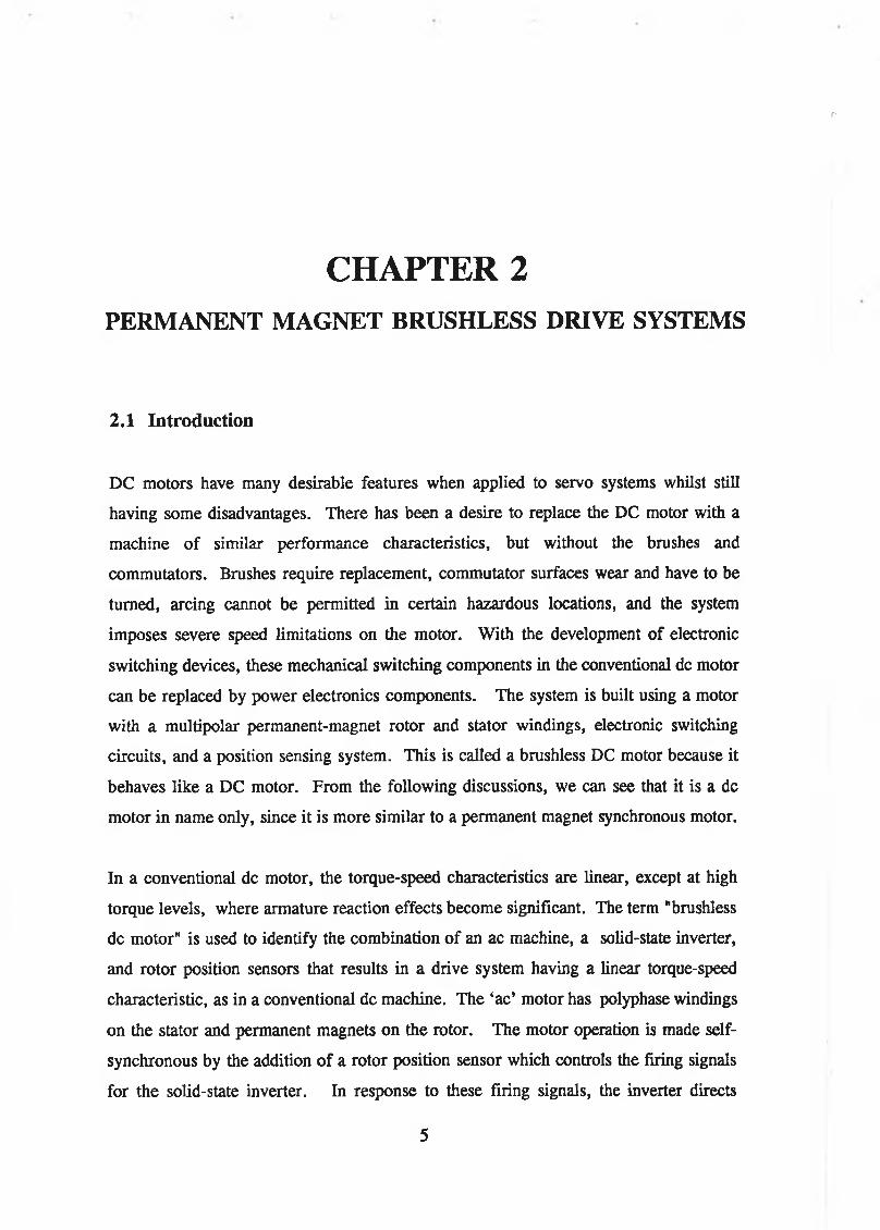
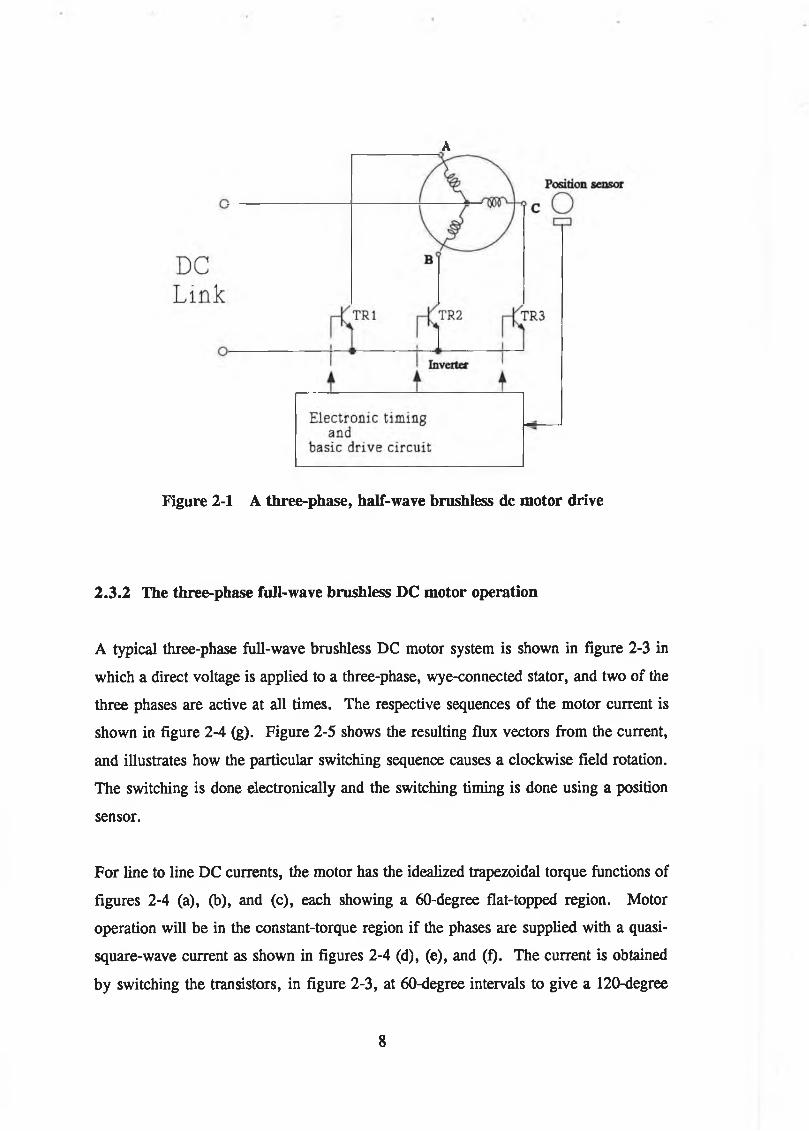
2.3.1 The three-phase half-wave brushless DC motor drive
For economic reasons, the three-phase half-wave brushless DC motor drive is often
selected because the cost of the electronic package is lower than that of the three-phase
full-wave brushless motor.
Figure 2-1 shows a basic three-phase half-wave brushless DC motor system The three
stator phases are wye-connected with the neutral point joined to the positive terminal of
the DC supply. Transistors TR1, TR2, and TR3 deliver unidirectional phase currents
in response to base drive signals which are under the control of the rotor position sensor.
This simple half-wave circuit is unusual in that there are no free-wheeling or feedback
diodes to provide an alternative path for the inductive winding current when a transistor
is turned off. Figure 2-2 shows a switching process of transistors and the current flow
in one phase each time.
7
A
Figure 2-1 A three-phase, half-wave brushless dc motor drive
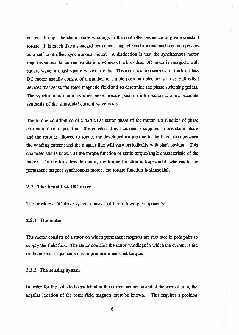
2.3.2 The three-phase full-wave brushless DC motor operation
A typical three-phase full-wave brushless DC motor system is shown in figure 2-3 in
which a direct voltage is applied to a three-phase, wye-connected stator, and two of the
three phases are active at all times. The respective sequences of the motor current is
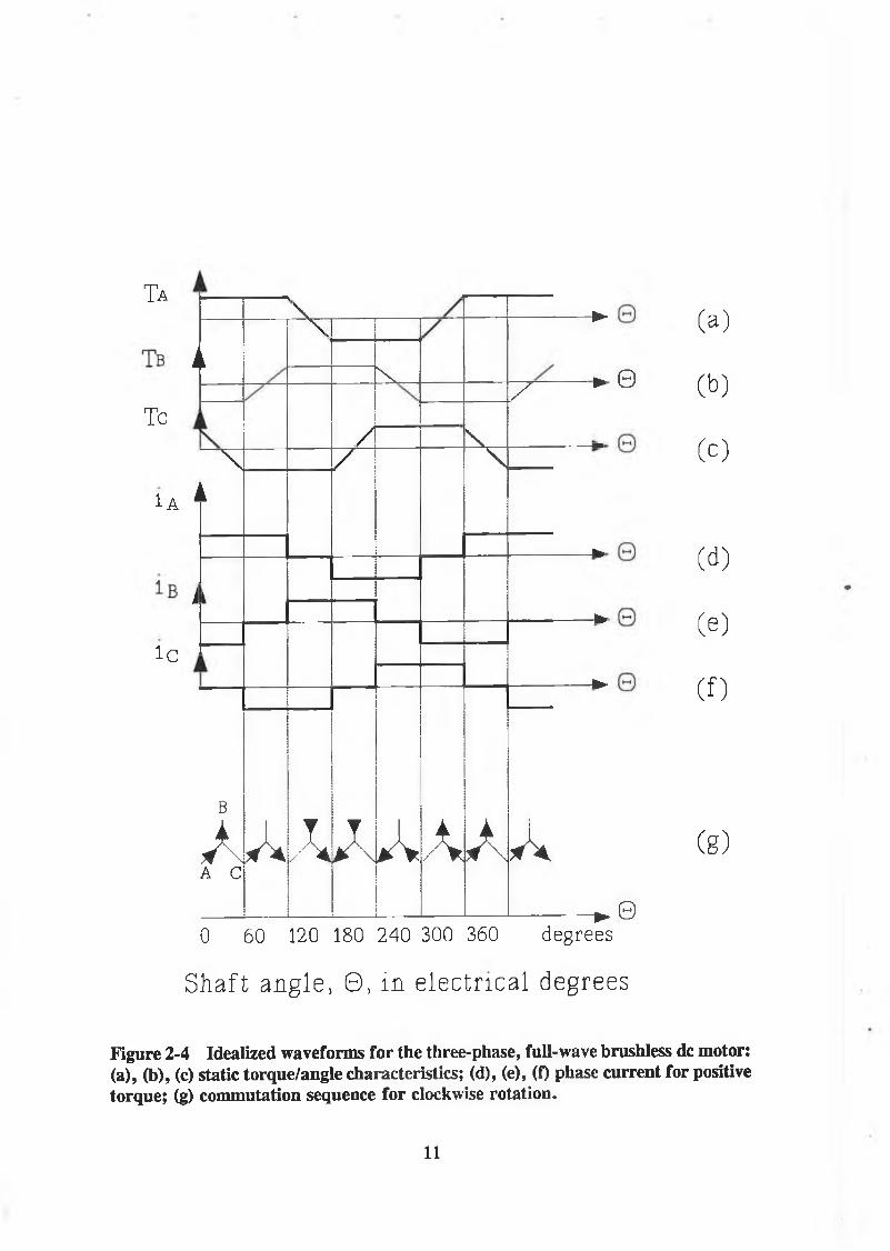
shown in figure 2-4 (g). Figure 2-5 shows the resulting flux vectors from the current,
and illustrates how the particular switching sequence causes a clockwise field rotation.
The switching is done electronically and the switching timing is done using a position
sensor.
For line to line DC currents, the motor has the idealized trapezoidal torque functions of
figures 2-4 (a), (b), and (c), each showing a 60-degree flat-topped region. Motor
operation will be in the constant-torque region if the phases are supplied with a quasi
square-wave current as shown in figures 2-4 (d), (e), and (f). The current is obtained
by switching the transistors, in figure 2-3, at 60-degree intervals to give a 120-degree
8
Figure 2-2 Three switch positions of the three-phase half-wave brushless DC motor
conduction angle. Each transistor switching occurs in response to the rotor position
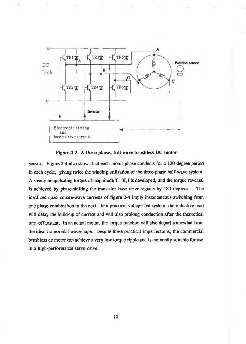
Figure 2-3 A three-phase, full-wave brushless DC motor
sensor. Figure 2-4 also shows that each motor phase conducts for a 120-degree period
in each cycle, giving twice the winding utilization of the three-phase half-wave system.
A steady nonpulsating torque of magnitude T=KXI is developed, and the torque reversal
is achieved by phase-shifting the transistor base drive signals by 180 degrees. The
idealized quasi-square-wave currents of figure 2-4 imply instantaneous switching from
one phase combination to the next. In a practical voltage-fed system, the inductive load
will delay the build-up of current and will also prolong conduction after the theoretical
turn-off instant. In an actual motor, the torque function will also depart somewhat from
the ideal trapezoidal waveshape. Despite these practical imperfections, the commercial
brushless dc motor can achieve a very low torque ripple and is eminendy suitable for use
in a high-performance servo drive.
10
T a
T e
l A
l e
k
I S .
V
---------------- ►
/ \
X *
\
A
/ \
to-
i tto-
— ►
B
AA C
A A A A A A A
----------------- ►
0
0
(a)
(b)
(c)
(d)
(e)
(f)
(g)
0 60 120 180 240 300 360 degrees
Shaft angle, 0 , in electrical degrees
Figure 2-4 Idealized waveforms for the three-phase, full-wave brushless dc motor: (a), (b), (c) static torque/angle characteristics; (d), (e), (O phase current for positive torque; (g) commutation sequence for clockwise rotation.
11
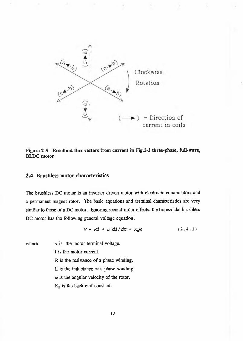
Figure 2-5 Resultant flux vectors from current in Fig.2-3 three-phase, full-wave, BLDC motor
2.4 Brushless motor characteristics
The brushless DC motor is an inverter driven motor with electronic commutators and
a permanent magnet rotor. The basic equations and terminal characteristics are very
similar to those of a DC motor. Ignoring second-order effects, the trapezoidal brushless
DC motor has the following general voltage equation:
v = Ri + L d i / d t + Keio ( 2 . 4 . 1 )
where v is the motor terminal voltage,
i is the motor current.
R is the resistance of a phase winding.
L is the inductance of a phase winding.
Co is the angular velocity of the rotor.
Ke is the back emf constant.
12
As stated already, the trapezoidal motor develops a torque of KTi, where KT is the torque
constant. The dynamic equation is:
T = K j l = J dco/dt + DU + Tf + Tl ( 2 . 4 . 2 )
where J is the total system inertia
D is the viscous damping coefficient
Tf is the frictional torque
Tl is the load torque.
Equation (2.4.1) and (2.4.2) are the usual DC machine equations, and within the
international system of units (SI), the values of KE and Kx are numerically equal.
The combination of the inverter, rotor position sensor and the brushless motor constitutes
an electronic commutator in which the inverter DC link voltage and current correspond
to the armature voltage and current of the motor. Consequently, the brushless DC motor
can employ standard DC drive techniques for speed and torque control. Thus the
average DC link voltage for the inverter can be controlled by a series transistor acting
as PWM regulator. In this manner, the voltage supplied to the electronic commutator
is varied and motor speed is controlled. This approach is clearly analogous to speed
control by armature voltage regulation of a DC motor. It is more usual to operate a DC
motor with an inner current loop that gives direct torque control, and in the brushless
DC system, a series transistor regulator in the DC link can operate in a current-
controlled PWM mode. However, this external transistor is not really necessary because
the main inverter transistors can regulate the amplitude of the motor current by PWM
control as well as commutating the current from phase to phase at the appropriate shaft
positions. Current sensing is required in the motor leads, and the current feedback
signal is used in a conventional PWM current loop. These controllers are now available
in integrated circuit form for brushless DC motor applications which will be discussed
later.
2.5 Position sensing system
13
The rotor position sensors are an integral part of the brushless DC motor system. They
are used to indicate the intermediate position of the rotor so that appropriate switching
signals can be generated for the inverter. For small motors, the rotor position sensors
are usually mounted on the inside surface of the stator, whilst for larger motors, they
are usually a separate unit fixed onto the non-drive end of the shaft. There are several
types of rotor position sensors; hall effect sensors, electro optical sensors, resolvers,
and digital encoders are the most commonly used device. For brushless DC motors,
hall effect sensors are normally selected to detect the magnitude and direction of
magnetic fields. Motors require three of these sensors symmetrically mounted on the
stator. The output signals from the sensors are processed to provide the position signals
required for the base device circuits to switch the transistors in the inverter.
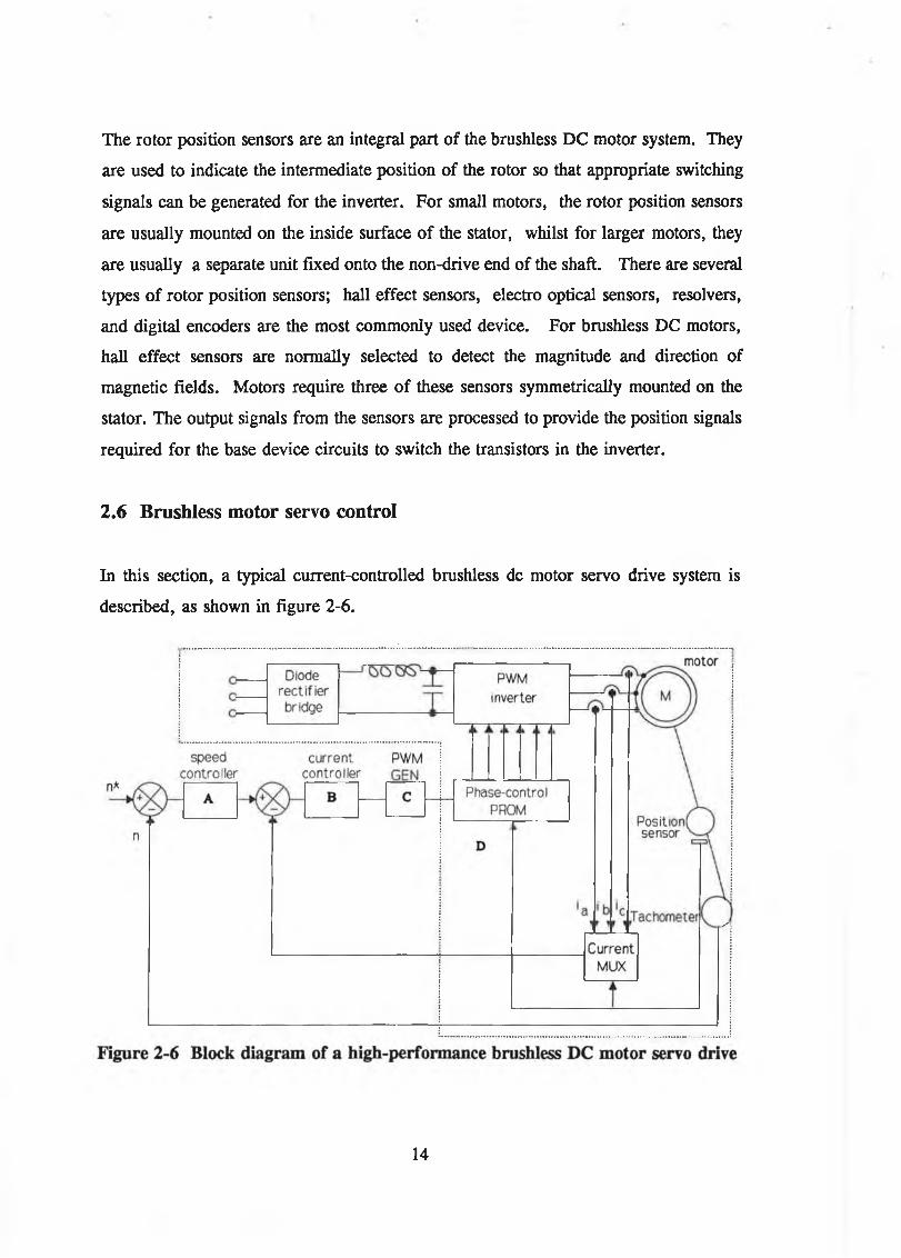
2.6 Brushless motor servo control
In this section, a typical current-controlled brushless dc motor servo drive system is
described, as shown in figure 2-6.
14
Precise control of the motor speed is achieved by a classical double-loop control scheme
with an outer high-gain speed loop and an inner current loop. For the sake of
discussion, the major portions of the system are labelled A through D and described as
follows.
1. Speed loop (A)
The speed loop adjusts the motor torque to ensure that the motor speed follows the input
command. The magnitude and polarity of the set speed command represent the desired
motor speed and direction of rotation, respectively. This signal is compared with the
tachometer signal to produce a speed error that is fed to the speed loop A. Normally,
the tachometer used in a brushless drive is itself brushless. The speed loop is
compensated in various ways, such as with lead and lag networks or PID techniques, to
ensure stable operation and to allow a dynamic match of the drive system to the load.
As in the classical DC servo drive, the compensated speed error is the demanded current
and hence the demanded torque in the motor. The negative value of the speed error
signifies a negative torque demand and, in the brushless DC motor, this torque reversal
is achieved by energizing each motor phase in the negative-torque region of the static
torque/angle characteristic. Therefore the servo drive can be controlled in all four
quadrants.
B. Current controller (B)
The current loop gives a signal to the PWM generator to ensure that the motor current
follows the motor torque command. In figure 2-8, the current from the speed loop is
compared with the actual current by multiplexing the current feedback signals from the
three phases into one loop. The error signal is fed into the current loop which is also
compensated in the same manner as the speed loop, with lead and lag networks, to
ensure a fast and accurate response during load variations.
C. PWM generator (C)
15
The PWM generator is used to generate base drive signals for the inverter transistors.
This loop is implemented using a usual current-controlled PWM technique, in which the
amplified current error is fed to a comparator circuit with a fixed-frequency triangular
wave of several kilohertz. The comparator functions as a PWM generator and delivers
PWM waveforms whose duty cycle varies with the current error.
D. Brushless motor drive system (D)
Block D includes a brushless dc motor, power supply (uncontrolled diode bridge rectifier
and filter), inverter, position sensing system and tachometer. The PWM signals and
the position sensor signals are fed to a programmable read only memory (PROM), as
shown in figure 2-8. This phase control PROM stores a table containing the correct
state (on or off) of each transistor for each position of the shaft and for positive and
negative torque. Therefore, positive and negative torque can be developed with a
magnitude determined by the demanded current.
The current controlled brushless DC motor servo drive system gives full four-quadrant
operation of the brushless DC motor. When the speed is reduced suddenly, the negative
speed error results in a large braking torque and rapid deceleration of the motor, and the
energy is regenerated through the power inverter to the DC link. This regenerated
energy must be dissipated in a dynamic braking resistor across the DC link.
This brushless DC motor servo drive can be used for high-performance industrial servo
systems due to its static stiffness and low speed torque smoothness. The dynamic
characteristics of the drive can equal or excel those of conventional DC brush servo
drives with PWM transistor amplifiers. Compared with sinusoidal brushless drives, the
cost advantage of the motor can be emphasized because a low-resolution sensor will
suffice to detect the phase switching points. In addition, for a given shaft torque, the
peak current demand is less in a trapezoidal system than a sinusoidal system, and
therefore a lower current capacity is required by the inverter. Although the brushless
DC motor can have a much greater torque ripple than the sinusoidally based system or
the induction motor, the careful magnetic circuit design of the trapezoidal machine and
16

the use of rare earth materials result in satisfactory torque smoothness. The effects of
any residual ripple can be suppressed by the closed-loop action of the velocity and
current feedback loop, to give excellent low-speed performance. Torque smoothness and
static stiffness are perfectly satisfactory for servo applications in machine tools and
robotics. Because of its simplicity, low cost, and good performance characteristics, the
trapezoidal brushless dc motor is a major contender in the field of high-performance
servo drives.
17
CHAPTER 3DESIGN OF THE DIGITAL SPEED CONTROLLER
3.1 Introduction
The previous chapter described the permanent magnet brushless DC motor with a typical
current control servo system. In early applications of the brushless servo motor, the
electronic control systems were always built using analogue components. With the
development of the microprocessor, especially the digital signal processor(DSP), the
controller can now be designed more precisely and more flexibly using digital
techniques.
This thesis presents a digital speed controller for a permanent magnet brushless DC
servo drive. The design is based on an existing analogue system and it is implemented
by a digital signal processor, the TMS320C30. Digital controllers have many
advantages over analogue controllers.
• They are not affected by component ageing and temperature drift and they
provide stable performance.
• When the design is done in the z-domain, the behaviour of digital controllers
can be more precisely controlled.
• Digital controllers are programmable, thus making them more easy to
upgrade.
18
• They can be timeshared to implement different functions in the system, like
notch filters and system control,thus reducing system cost.
The controller is designed using two schemes, one directly in the z-plane, and the other
in the continuous domain which is converted into a digital form. The speed of the
TMS320C30 processor is very fast, so a short sample time can be selected such as 100
Hs or less. Due to the small interval, the delay of the ZOH (zero-order hold) can almost
be neglected and so the behaviour of the system is similar to that of an analogue system.
Obviously, if the sampling rate is fast enough, the sample period approaches zero, and
the speed response of the digital control system approaches that of the continuous
system. Therefore we use a design scheme, "analogue design of discrete controller",
which is appropriate for the TMS320C30 due to its fast speed. The design of a speed
controller using well known analogue control technology is described first. The
controller is then transformed into a digital form using the Tustin’s transformation [3-2].
An alternative speed controller using a direct digital design is also described. This
controller uses a feedback PID implementation in which the parameters are adjusted
using a graph-analytical method of pole-placement. This controller has a faster dynamic
response and better performance than conventional PID controllers. Both designs are
based on an AEG BHT brushless servo drive system. The modelling of the analogue
drive system is detailed in appendix A. The model simplification is described in section
3.3 and this is used for both designs.
3.2 The servo system model
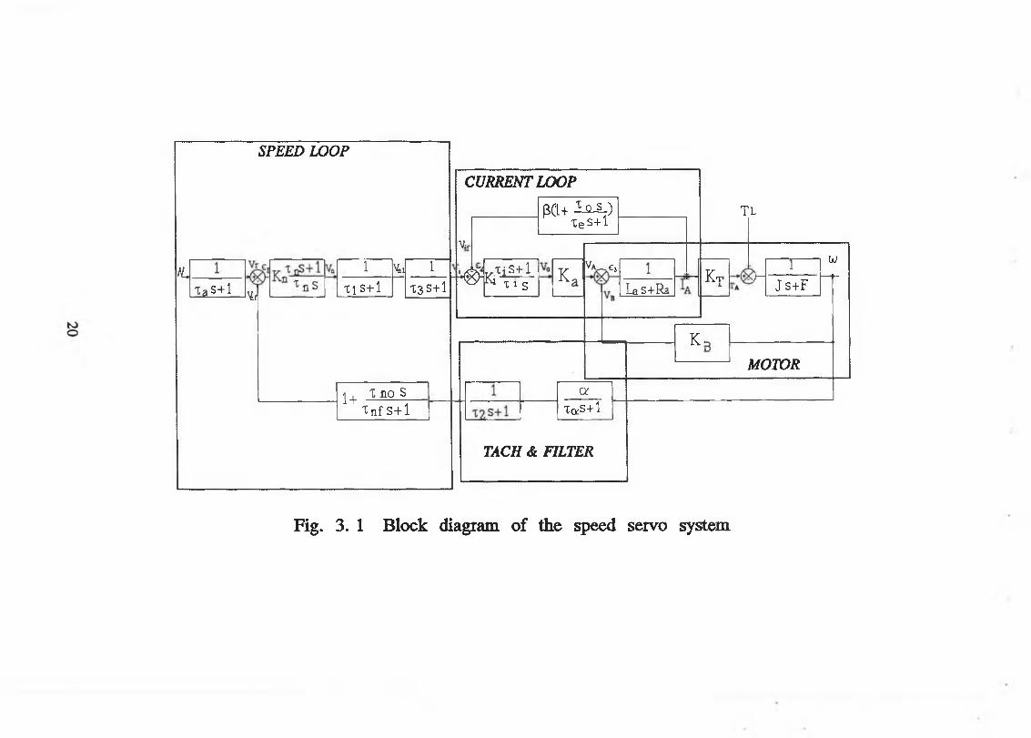
The servo drive selected for this project is one of the AEG BHT brushless motor series.
It is a current-controlled brushless DC servo system, and as already stated it generally
consists of a double closed loop control, ie, an inner current loop and an outer speed
loop as shown in Fig 2-8. The whole analogue servo system model is shown in figure
3-1. The modelling procedure is described in detail in appendix A.
19
S P E E D L O O P
AL
TaS+1 Yfl
1 \\ 1XI s+1 X3S+1
1+ X no S Xnf S+l
C U R R E N T L O O P
V,
PCL+ iiUL) xes+l
w -tiS±l Kl X 1 s K,
Va- c,
LaS+Ra
TL
Kn .1 bJ
/Js+F
a
Tq/S+ 1
K,M O T O R
T A C H & F I L T E R
Fig. 3. 1 Block diagram of the speed servo system
3.3 Simplifying the mathematical model
For the purpose of the design, the complex system model can be simplified into an
equivalent lower order transfer function.
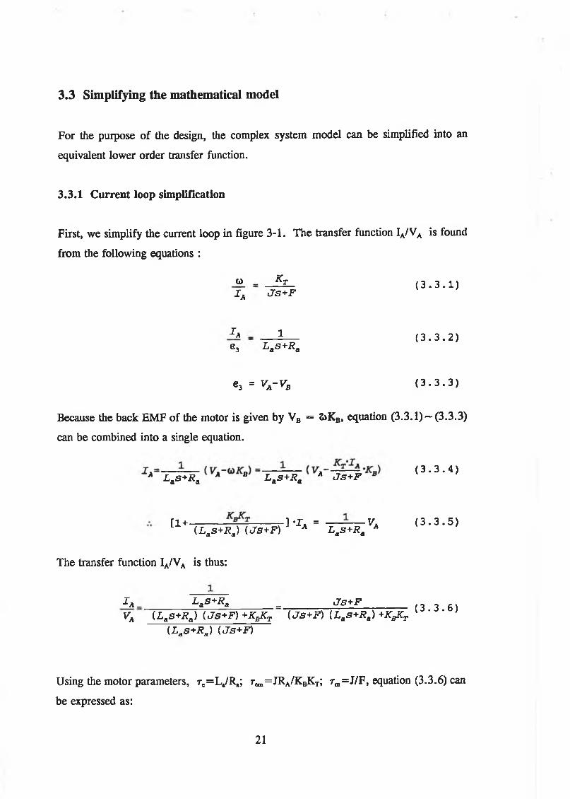
3.3.1 Current loop simplification
First, we simplify the current loop in figure 3-1. The transfer function IA/VA is found
from the following equations :
(i) K fI A J s + F
I A _ 1
e3 Las + R a
( 3 . 3 . 1 )
( 3 . 3 . 2 )
e3 = VA- V B ( 3 . 3 . 3 )
Because the back EMF of the motor is given by VB = S>KB, equation (3.3.1) — (3.3.3)
can be combined into a single equation.
( 3 . 3 . 4 )A LaS+Ra A B LaS+Ra A J S + F
[1 + ------------------- ] -J, = V. ( 3 . 3 . 5 )(L aS+Ra) {JS+F) A LaS +Ra A
The transfer function IA/VA is thus:
I A _ LaS +Ra _ J s + FVA (L aS+Ra) (JS+F) +KbKt (JS+F) (LaS+Ra) +KgKT
(LaS+Ra) (J s+ F )
( 3 . 3 . 6 )
Using the motor parameters, re=L,/R,; rem=JRA/KBKT; rm=J/F, equation (3.3.6) can
be expressed as:
21
A _ ^ < V +1)
V U W e ® 2* X*ws+ I* Ie S !s + l ° i 2 + 1 ] ( 3 . 3 . 7 )
In equation (3.3.7), the t o t and re are very small time constant. For the servo system,
1 h m and l/re are much greater than the system crossover frequency foc, hence the term
TOTres2 can be ignored. The term (reO /T m is much smaller than rm and the term TmlTm
« 1, so they can also be ignored, and equation (3.3.7) can be simplified as:
I * ± T6jL( Tmg+1) (3.3.8)
This represents the motor transfer function in the current loop as shown in figure 3-2.
Motor
Fig. 3-2 The block diagram of the current loop
Next we can simplify the current loop in figure 3-2 into an equivalent transfer function.
Ki’Ka"Cea(xi s+ l) (xms+1)= ----------------------TyR.a—rn-------------------------------------- ( 3 . 3 . 9 )
x i S ( T alBS + l ) + - i ^ F ^ S 5 [ l + ( T 0 +Xi ) s ] ( t mS + l )
22
Substituting K=(KiKjSTem)/(TmRJ into equation (3.3.9) gives:
T -^(-CjS+1 ) ( x _ s + l )_£a = ______________ P j ' a ______________ ( 3 . 3 . 1 0 )v x ( X jx m+ t t 0T am+Ktax i ) S 2+ (T i+ K to + K T i+ K x J S+ K
Because < < K iTo^+ rj.J and r;< < K(T0+ 7 ; + r J , equation (3.3.10) can be
approximated as:
^ - j ^ g + l ) (Ta a + i )
VI i f i T o T ^ + T ^ ) s 2+JC(t0+ t j + t J s+iT
• i ( X j S + 1 ) ( t ^ s + l ) ( 3 . 3 . 1 1 )
[ ( T 0+Tjr) S + l ] (XmS + 1 )
TjS + 1i T u ^ + x ^ T s + i T
This simplified transfer function represents the current loop and the motor windings.
3.3.2 Filters and tachogenerator simplification
At this point, we substitute the parameters of BHT servo system in Appendix A into the
system block diagram, as shown in figure 3-4. The transfer function of the filter in
block 4 cancels the numerator of the current loop transfer function.
Block 12 and block 13 in the feedback loop can be combined and simplified as follows:
23
Block 1 Speed loop Block3 Block4 C urrent loop Motor
Fig. 3-4 The transfer function block diagram of the servo system
1 0 . 0 4 3 5O.OOls+1 0 . 003S+1
=______ 0 . 0435______ 12)3 x l 0 ”6S2+0 . 004S+1
A 0 . 0 4 3 5 0 . 004S+1
where the coefficient of the term s2, much smaller than 1/S>C (crossover frequency of the
system), is neglected.
This feedback combination may be replaced by two transfer functions in the forward
path as shown in figure 3-5.
The leftside transfer function, 0.0435/(0.004s+l) can be cancelled by block 1, and
hence the whole servo system model can be simplified into figure 3-6.
Finally, in figure 3-6, the intermediate three blocks can be simplified to a single block
24
Fig. 3-5 The transferring feedback block to forward path
Fig. 3-6 The simplified block diagram of Fig. 3-4
as shown in figure 3-7 and described below:
0 . 0 4 3 5 . 1 . 0 . 5990 . 0 0 0 4 5 + 1 0 . 0 0 0 2 5 + 1 0 . 003155+1
( 3 . 3 . 1 3 )„_______ 0 . 0435x0 . 599_________ 0 . 0 2 6
( 0 . 0 0 0 4 + 0 . 0 0 0 2 + 0 . 0 0 3 1 5 ) 5 + 1 “ 0 . 0037 55+1
where the second and third order terms are ignored because these time constants are
much smaller than 1/5>C.
25
▼e
Fig. 3-7. The simplified diagram of Fig. 3-6
3.3.3 The open-loop transfer function of the servo system
The open-loop transfer function of the servo system plant of figure 3-7 is of the
following form:
G ( s ) = ^ -----------r ( 3 . 3 . 1 4 )( E x s + 1 ) ( t „ s + 1 )
where = 0.026x140.3 = 36.48; E r= 0 .00375; rm = 2.571. Because rm> > E r and
it can be simplified as:
= -------, 5 * ,t ( 3 . 3 . 1 5 )t^sCSts+ 1 )
This simplified system model is used for the design of the digital controllers.
3. Analogue design o f the discrete controller
The actual controller can be designed in two different ways, either directly in the z-
plane or indirectly in the s- plane using well-developed analogue design techniques and
26
then converting it into a digital form. The AEG brushless servo system has a
conventional analogue PI controller which can be expressed as:
This is described in detail in appendix A. The PI scheme has been developed over
several decades, and there are many possible design methods. The following sections
will describe two of them. One is the minimum overshoot method and the other is an
optimal model method.
3.4.1 Minimum peak overshoot method [3-8]
This method selects a control law which makes the system dynamic response have a
minimum peak overshoot. The design procedure is based on a frequency response
technique in which the desired open-loop log magnitude characteristics is shown in figure
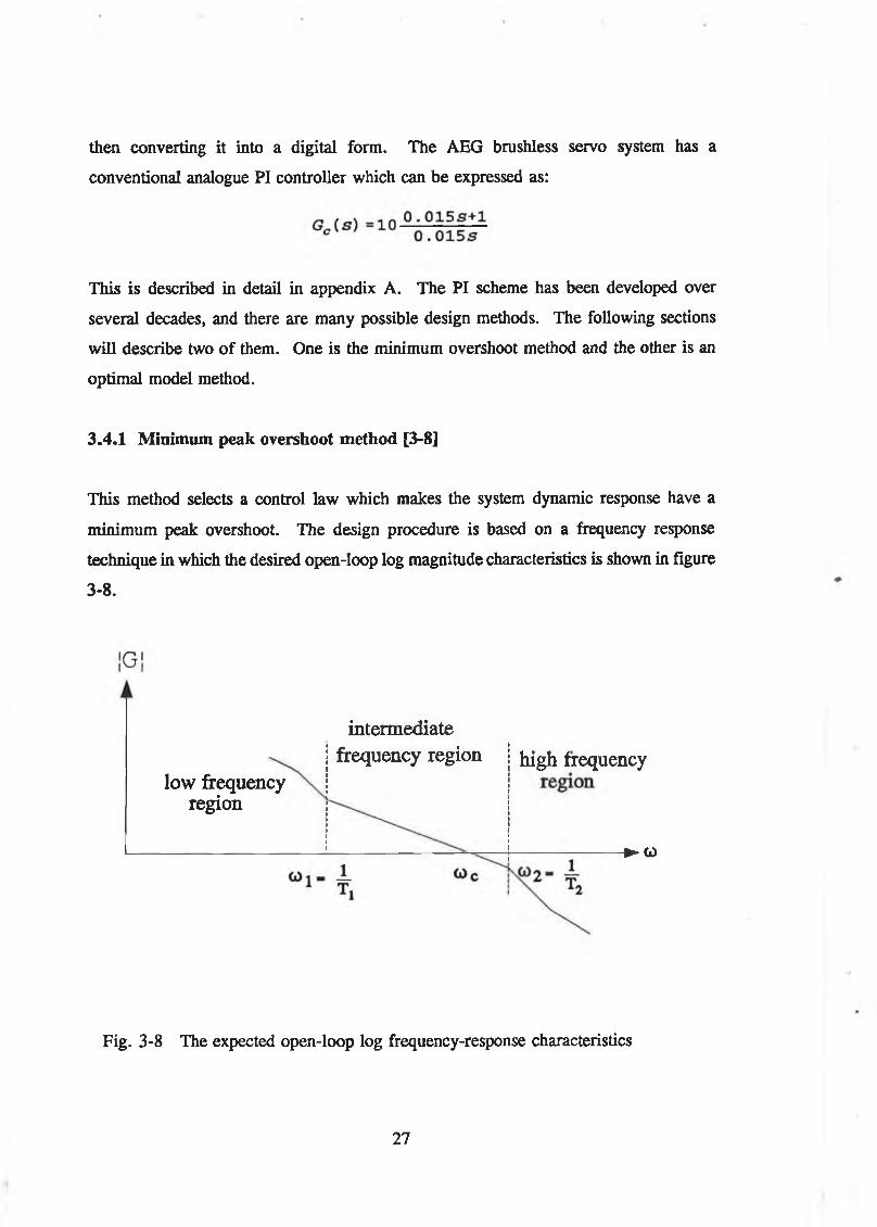
3-8.
intermediatefrequency region j high frequency
low frequency region
► 0)
Fig. 3-8 The expected open-loop log frequency-response characteristics
27
For figure 3-8, we should meet the following requirements.
1. In the medium frequency region, the -20db/decade goes through zero db and
should have a certain width to ensure the stability of the system.
2. The comer frequency must be big enough to give a fast system respqnse.
3. The gain in the low frequency region must be high enough to ensure static
accuracy.
4. The attenuation in high frequency region must be high enough to reject noise.
It is not easy to satisfy all the above requirements owing to the contradictions among
them, but if the servo system can be transformed into a typical Type 2 system, this issue
can be solved. For the Type 2 system, the open-loop transfer function of the system is
expressed as:
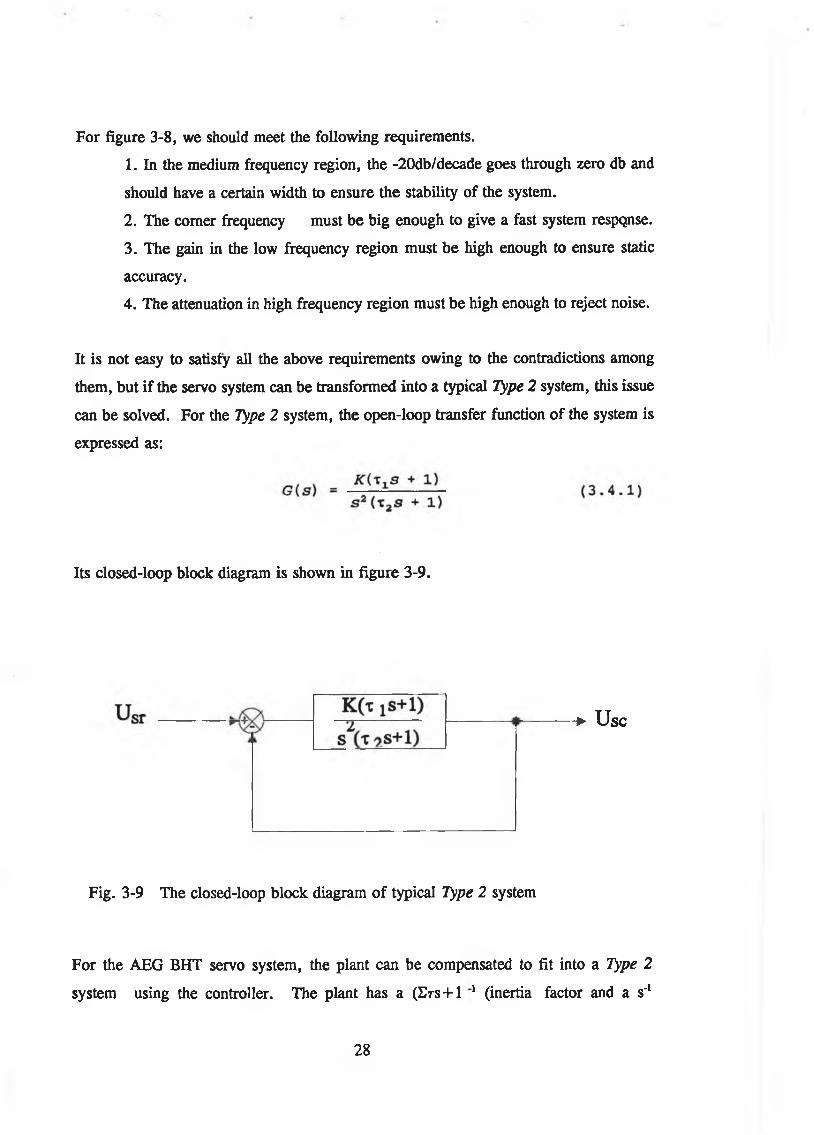
Its closed-loop block diagram is shown in figure 3-9.
Fig. 3-9 The closed-loop block diagram of typical Type 2 system
For the AEG BHT servo system, the plant can be compensated to fit into a Type 2
system using the controller. The plant has a (Ers+1 1 (inertia factor and a s'1
► Use
28
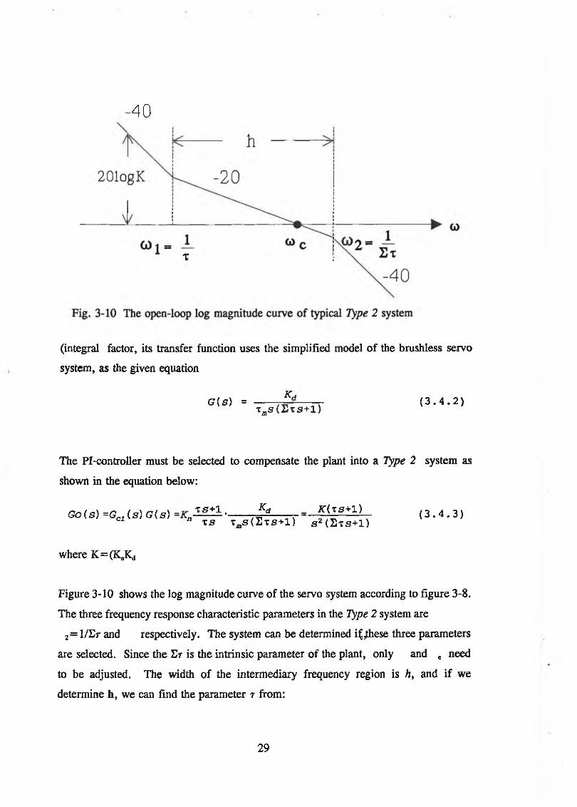
■40
(integral factor, its transfer function uses the simplified model of the brushless servo
system, as the given equation
G ( s ) =Ka
•cffls ( E x s + l )( 3 . 4 . 2 )
The Pl-controller must be selected to compensate the plant into a Type 2 system as
shown in the equation below:
T g + 1 . Kd _ K ( x s + 1)'n t s ^ ( S - r s + l ) s 2 ( S t s + 1 )
g o ( s ) =g c1( S ) G ( S ) . 0 . 4. 3)
where K=(KnKd
Figure 3-10 shows the log magnitude curve of the servo system according to figure 3-8.
The three frequency response characteristic parameters in the Type 2 system are
2=1 /Er and respectively. The system can be determined i^Jhese three parameters
are selected. Since the Er is the intrinsic parameter of the plant, only and c need
to be adjusted. The width of the intermediary frequency region is h, and if we
determine h, we can find the parameter r from:
29
h .“ I - _E_ col “ S t
( 3 . 4 . 4 )
From figgure 3-10, we have
So,
20 logic = 401090)1+20109— - = 20109»!»,.» 1
2C = CDjto
( 3 . 4 . 5 )
( 3 . 4 . 6 )
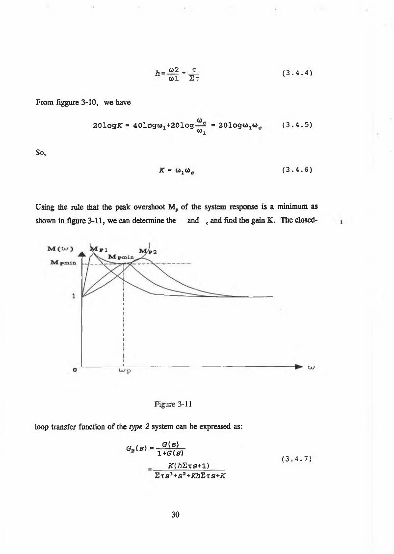
Using the rule that the peak overshoot Mp of the system response is a minimum as
shown in figure 3-11, we can determine the and c and find the gain K. The closed-
Figure 3-11
loop transfer function of the type 2 system can be expressed as:
G A s) =_ g ( s )1 +G(s)
K{hHzs+l)E t s 3+s 2 +JG2Et s +JC
( 3 . 4 . 7 )
30
Gfl(j<o) = --------- K U + j h L x a ) — ( 3 .4 . 8 )(Rf~<i) ) +j (KtiLt -E t co2) co
where the overshoot can be expressed by the amplitude of GB(jS>
M ( < j i , K ) = |Gb ( j w ) |
= _______________ kJi +A2S t 2(j2_______________ ( 3 . 4 . 9 )v / S t 2w 6+ ( l - 2 K h ' L x 2)<J>i + (K2h 2H^z -2 K ) oi 2+ K2
The frequency response form of equation (3.4.7 is:
Whena w dMp
-ïp. =0 , we can obtain MP as a function of K, and letting =0 we can
obtain the minimum peak overshoot of the closed-loop system as shown in figure
3-11. At the point of the there are optimal ratios of S>2 / 5>c and / which
are expressed as functions of h [3-8]:
w2 _ 2 htoc h+1
Wç = h+i 2
( 3 . 4 . 1 1 )
( 3 . 4 . 1 2 )
The with respect to h can be expressed as:
( 3 . 4 . 1 3 )h - l
By selecting different values of h, the corresponding Mp , and / values can be
derived and are given in table 3.4.1 [3-8].
31
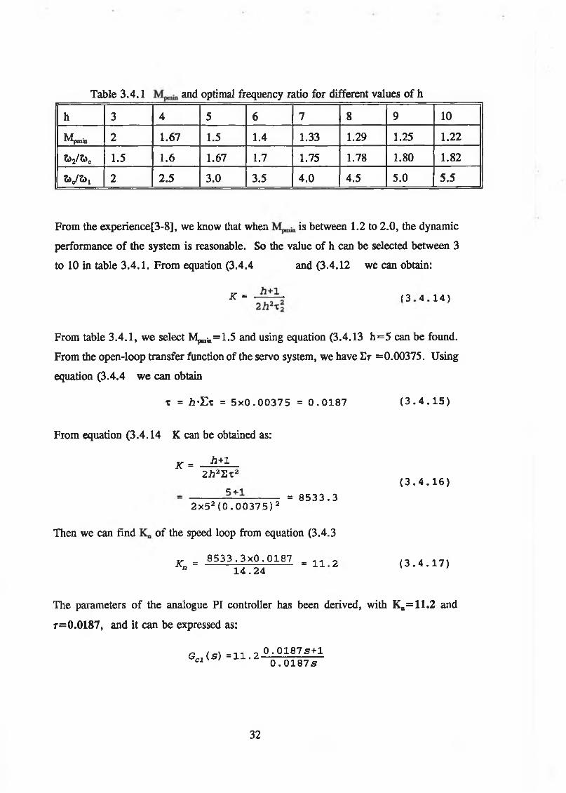
Table 3.4.1 and optimal frequency ratio for different values of h
h 3 4 5 6 7 8 9 10
pmin 2 1.67 1.5 1.4 1.33 1.29 1.25 1.22
5>2/3>e 1.5 1.6 1.67 1.7 1.75 1.78 1.80 1.82
V i> i 2 2.5 3.0 3.5 4.0 4.5 5.0 5.5
From the experience[3-8], we know that when is between 1.2 to 2.0, the dynamic
performance of the system is reasonable. So the value of h can be selected between 3
to 10 in table 3.4.1. From equation (3.4.4 and (3.4.12 we can obtain:
K = — — (3 4 14 )
From table 3.4.1, we select Mpmin=1.5 and using equation (3.4.13 h=5 can be found.
From the open-loop transfer function of the servo system, we have Er =0.00375. Using
equation (3.4.4 we can obtain
x = h - L x = 5 x 0 . 0 0 3 7 5 = 0 . 0 1 8 7 ( 3 . 4 . 1 5 )
From equation (3.4.14 K can be obtained as:
h+1K =2 A 2 2 xz
E 0 . 1
= 8 5 3 3 . 3( 3 . 4 . 1 6 )
2 x 52 (0 . 00375 ) 2
Then we can find of the speed loop from equation (3.4.3
K = 8 5 3 3 - 3 x 0 . 0 1 8 7 = X1 2 ( 3 . 4 . 1 7 )71 1 4 . 2 4
The parameters of the analogue PI controller has been derived, with K„=11.2 and
r = 0.0187, and it can be expressed as:
G c j ( s)=11.2 0 ^ 1 8 7 £ l lC1 0 . 0 1 8 7 s
32
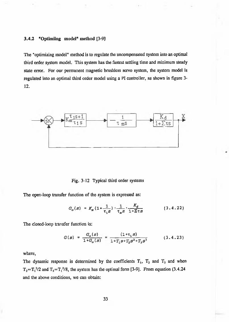
3.4.2 "Optimiing model" method [3-9]
The "optimizing model" method is to regulate the uncompensated system into an optimal
third order system model. This system has the fastest settling time and minimum steady
state error. For our permanent magnetic brushless servo system, the system model is
regulated into an optimal third order model using a PI controller, as shown in figure 3-
12.
Fig. 3-12 Typical third order systems
The open-loop transfer function of the system is expressed as:
G0 ( s ) = Km( 1 + — ) •— •° m T1S T mS 1 + Ï T S
The closed-loop transfer function is:
G J s )G ( s ) =
( 1 +T1 S)i + g 0 ( s ) i + r 1 s + r 2s 2 + r 3 s 3
( 3 . 4 . 2 2 )
( 3 . 4 . 2 3 )
where,
The dynamic response is determined by the coefficients T1} T2 and T3 and when
T2= T t2/2 and T3=T i3/8, the system has the optimal form [3-9]. From equation (3.4.24
and the above conditions, we can obtain:
33
r, « TlT"2 % ( 3 . 4 . 2 4 )
r 3 =
t ^ E r ; J r .-2^ ( 3 . 4 . 2 6 )
Substituting equation (3.4.26 and (3.4.24 to equation (3.4.23 we have the optimal
third order transfer function:
G t s ) = __________ l + 4 S T g __________ ( 3 . 4 . 2 7 )1+4Et s +8St2£T2 + 8St3S3
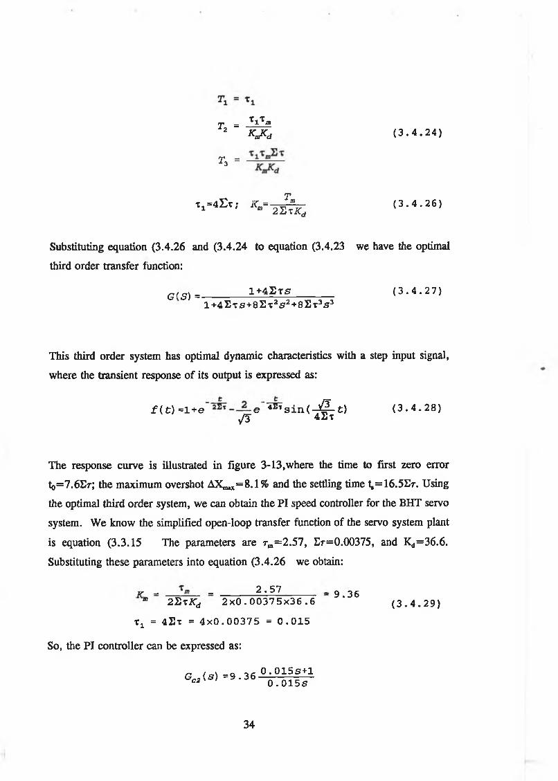
This third order system has optimal dynamic characteristics with a step input signal,
where the transient response of its output is expressed as:
f ( t ) = l + e e ^ s i n i - ^ - 1 ) ( 3 . 4 . 2 8 )v/J 4Et
The response curve is illustrated in figure 3-13,where the time to first zero error
to=7.6Er; the maximum overshot AXmilx=8.1% and the settling time t,=16.5Er. Using
the optimal third order system, we can obtain the PI speed controller for the BHT servo
system. We know the simplified open-loop transfer function of the servo system plant
is equation (3.3.15 The parameters are rm=2.57, E r=0.00375, and Kd=36.6.
Substituting these parameters into equation (3.4.26 we obtain:
zr — _ 2 . 57_______ _ g j gm 2 2 x 2 ^ 2 x 0 . 0 0 3 7 5 x 3 6 . 6 ’ ( 3 . 4 . 2 9 )
X1 = 4 S t = 4 x 0 . 0 0 3 7 5 = 0 . 0 1 5
So, the PI controller can be expressed as:
/ „ n _ o 0 . 0 1 5 S + 1 G« < s ) " 9 - 3 6 0 . 0 1 5 5
34

Fig. 3-13 The response curve of optimal third order system
Comparing both designed PI speed controllers, we can see that they are very similar.
They are also nearly same as the speed loop of the BHT system in appendix 1 which
proves that the analogue controller of the AEG system is well designed.
3.4.3 Discretiation of the analogue controller
The simplest method of obtaining the digital speed controller is directly to discretize the
analogue controller to a digital form. However, due to the digital controller having a
zero order hold, the accuracy and stability of the system can be effected. Fortunately,
since we use the very fast DSP-TMS320C30, this can be greatly reduced. The design
procedure is as follows:
(1 Design the controller Gc(s in the continuous-time domain.
(2 Determine the delay of the series connection of the leading sampler and the
35
ZOH (zero order hold which is approximated by a continuous transfer function
C ( s) = T ' 1. - T— = £ _ ( 3 . 4 . 3 0 )1 T s + 2 Ts+2
Where T 1 represents the transfer function of the sampler and 2T(Ts+2 '* is
Pade’s first approximation of the ZOH.
(3 Find the digital controller D(s in the continuous-time domain.
D ( s ) = ^ ( 3 . 4 . 3 1 )GapiS)
(4 Transform the adopted controller D(s transfer function to the z-plane by
using Tustin’s transformation [3-2].
[£>(3 ) ] ^ . ~ D ( z ) ( 3 . 4 . 3 2 )
(5 A combination of the continuous-time controller design and Tustin’s
transformation may yield a physically unrealizable system if there are poles at
z = l . It is usual to replace the excessive poles (z+1 by their d.c. gain as
(z+1 z=1=2.
(6 It may be necessary to adjust the open-loop transfer function gain in order to
meet the design requirements precisely.
Step 1: We have already obtained the analogue speed controller for the AEG BHT servo
system in the previous sections.
^ _ n ( 0 . 0 1 5 S + 1 )G« <s) “ o 7 o i 5 s
36
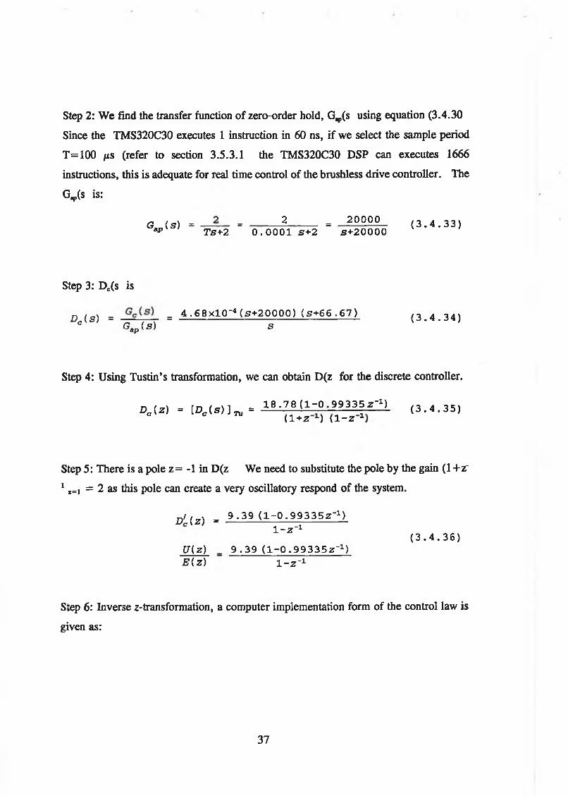
Step 2: We find the transfer function of zero-order hold, Gv(s using equation (3.4.30
Since the TMS320C30 executes 1 instruction in 60 ns, if we select the sample period
T=100 ¡is (refer to section 3.5.3.1 the TMS320C30 DSP can executes 1666
instructions, this is adequate for real time control of the brushless drive controller. The
G.p(s is:
G ( S ) = — — = ----------? --------- = 2 0 0 0 0 ( 3 . 4 . 3 3 )ap Ts+2 0 . 0 0 0 1 S + 2 s + 2 0 0 0 0
Step 3: Dc(s is
D, ( s ) = = 4 . 6 8 x 1 0 ~4 ( s + 2 0 0 0 0 ) ( g + 6 6 . 6 7 ) ( 3 . 4 . 3 4 )c ' ~ ' Gap( s ) S
Step 4: Using Tustin’s transformation, we can obtain D(z for the discrete controller.
1>„<z> = [Dc ( s ) ] „ = 1 8 . 7 e t 1 - 0 9 9 3 3 | z ^ > , , 3 . 4 . 3 5 ,(1 + z ■*•) (1 - z
Step 5: There is a pole z= -1 in D(z We need to substitute the pole by the gain (1 + z
1 Z=1 = 2 as this pole can create a very oscillatory respond of the system.
D 1 ( z ) = 9 . 3 9 ( 1 - 0 . 9 9 3 3 5 Z " 1 )
1 - z ~ x( 3 . 4 . 3 6 )
U ( z ) _ 9 . 3 9 ( 1 - 0 . 9 9 3 3 5 z ' 1 )
E ( z ) 1 - 2 - i
Step 6: Inverse z-transformation, a computer implementation form of the control law is
given as:
37
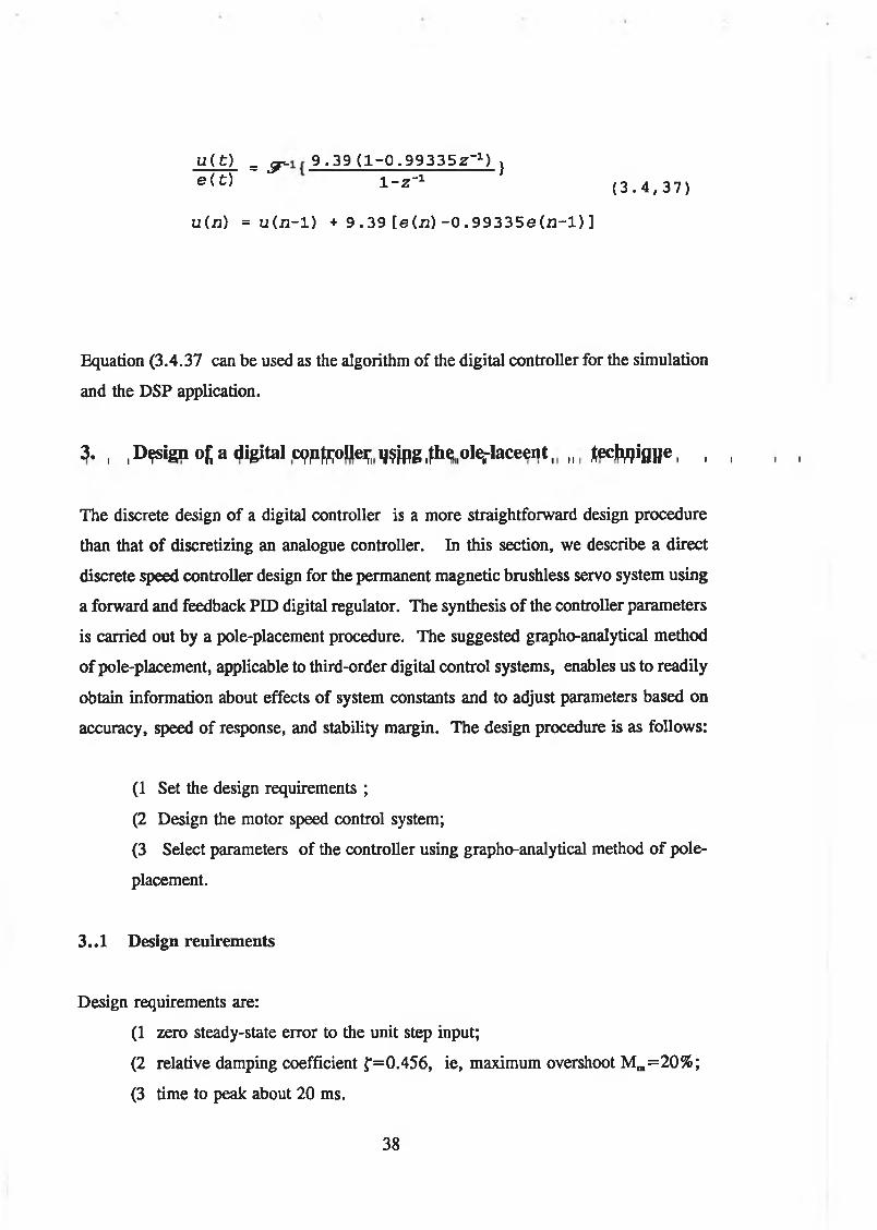
u ( t) = p . 9 .39 ( 1 - 0 . 9 9 3 3 5 Z ' 1) ^
e ( t ) 1 - 2 - 1 ( 3 . 4 , 3 7 )
u(n) = u ( n - l ) + 9 .39 [e(n) - 0 . 9 9 3 3 5 e ( n - l ) ]
Equation (3.4.37 can be used as the algorithm of the digital controller for the simulation
and the DSP application.
3. , .Design of a digital cpp^ollei^ ij^pg^he ol^laceent, „ techfliflHe ...........................
The discrete design of a digital controller is a more straightforward design procedure
than that of discretizing an analogue controller. In this section, we describe a direct
discrete speed controller design for the permanent magnetic brushless servo system using
a forward and feedback PID digital regulator. The synthesis of the controller parameters
is carried out by a pole-placement procedure. The suggested grapho-analytical method
of pole-placement, applicable to third-order digital control systems, enables us to readily
obtain information about effects of system constants and to adjust parameters based on
accuracy, speed of response, and stability margin. The design procedure is as follows:
(1 Set the design requirements ;
(2 Design the motor speed control system;
(3 Select parameters of the controller using grapho-analytical method of pole-
placement.
3..1 Design reuirements
Design requirements are:
(1 zero steady-state error to the unit step input;
(2 relative damping coefficient f=0.456, ie, maximum overshoot Mm=20%;
(3 time to peak about 20 ms.
38
3..2 Design the speed digital controller
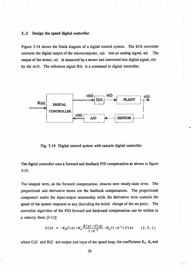
Figure 3-14 shows the block diagram of a digital control system. The D/A converter
converts the digital output of the microcomputer, u(n into an analog signal, u(t The
output of the motor, c(t is measured by a sensor and converted into digital signal, c(n
by the A/D. The reference signal R(n is a command to digital controller.
Fig. 3-14 Digital control system with cascade digital controller
The digital controller uses a forward and feedback PID compensation as shown in figure
3-15.
The integral term, as the forward compensation, ensures zero steady-state error. The
proportional and derivative terms are the feedback compensators. The proportional
component scales the input-output relationship while the derivative term controls the
speed of the system response to any (including the initial change of the set point. The
controller algorithm of the PID forward and backward compensation can be written in
a velocity form [3-11]:
U(z) = -KpC{z ) +KX J?(-z) ~°^zl - K ^ l - z - 1) C{ z ) ( 3 . 5 . 1 )1 - z 1
where C(Z and R(Z are output and input of the speed loop, the coefficients KP, Kj and
39
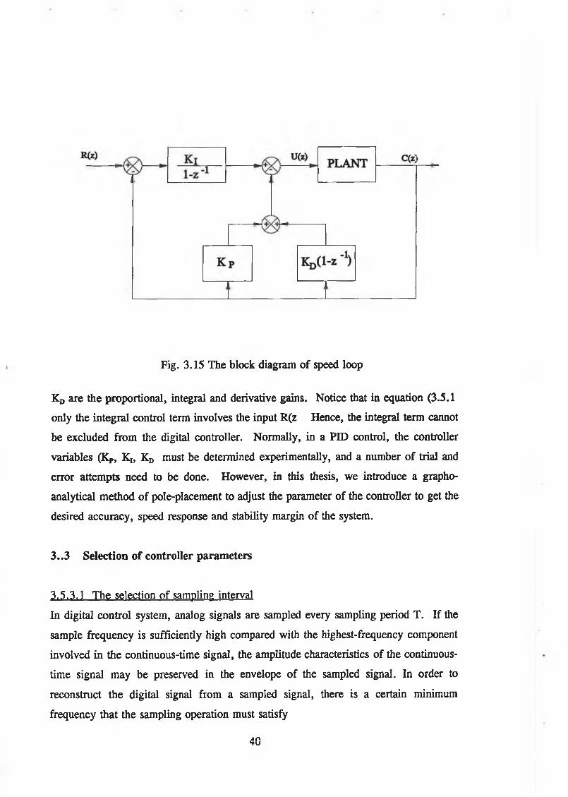
Fig. 3.15 The block diagram of speed loop
Kd are the proportional, integral and derivative gains. Notice that in equation (3.5.1
only the integral control term involves the input R(z Hence, the integral term cannot
be excluded from the digital controller. Normally, in a PID control, the controller
variables (K,, KI} KD must be determined experimentally, and a number of trial and
error attempts need to be done. However, in this thesis, we introduce a grapho-
analytical method of pole-placement to adjust the parameter of the controller to get the
desired accuracy, speed response and stability margin of the system.
3..3 Selection of controller parameters
3.5.3.1 The selection of sampling interval
In digital control system, analog signals are sampled every sampling period T. If the
sample frequency is sufficiently high compared with the highest-frequency component
involved in the continuous-time signal, the amplitude characteristics of the continuous
time signal may be preserved in the envelope of the sampled signal. In order to
reconstruct the digital signal from a sampled signal, there is a certain minimum
frequency that the sampling operation must satisfy
40
ClÌg > 2(JÌ1 ( 3 . 5 . 2 )
Where S>, is the sampling frequency, which is defined as 2x/T.
S>! is the highest-frequency component present in the continuous-time signal x(t
Normally, the sample time should be less than the smallest time constant in the plant
model, by factor 30 to 100 minimum [3-10]. For the BHT servo system the smallest
time constant is 3.75 ms, the sample interval T should be selected between
0.0375ms ~ 0.2ms. For our application, we selected T=0.1 ms.
3.5.3.2 The characteristic equation of the closed-loop system
We design the digital speed controller using the continuous parts of the brushless motor
servo system as the plant. The transfer function of the continuous part can be obtained
from equation (3.3.15 and it is expressed as:
Gp (a)Tas ( E T s + 1 )
( 3 . 5 . 3 )
The transfer function of zero-order hold can be expressed as:
( 3 . 5 . 4 )
We transfer the plant to digital form by using the z-transformation.
Gp ( z ) = C [Gzoh( s ) Gp ( s ) ] = K ( z + 1 )( 3 . 5 . 7 )
( z - P x ) ( z - P 2 )
where K=0.00186 Pj = l and P2= e rrT=0.947.
The closed-loop transfer function of the system is:
C ( z )R ( z )
KI Z2 Gp { z )( 3 . 5 . 8 )
( z - 1) z + { K p z ( z - 1) +Kt z 2+Kd ( z - l ) 2}Gp ( z )
41
z ( z - l ) + [ K p z ( z - l ) + K j Z 2 +Kd ( z - 1 ) *] Gp (z) = 0 ( 3 . 5 . 9 )
Substituting Gp(z from equation (3.5.7 into (3.5.9 and then simplifying (3.5.9 into
the polynomial form, one can obtain, after simple manipulations
z 4 + a2z 3 + a2z 2 + axz + a 0 = 0 ( 3 . 5 . 1 0 )
where
a3=K(KP+K I+K D
a2= PlP2 + (Pl+P2 Da1=KKD-K(KP+2KD
a o = K K D
Notice that: when KD=0, the coefficient ao is zero and the system characteristic
equation becomes
Z 3 +A2Z 2 +A1Z + A 0 = 0 ( 3 . 5 . 1 1 )
where A2=K(KP+K I 1 +P2 i
Ai=p1p2+(pi+p2 A0=-p1p2-KKp=-0.974-0.0186Kp
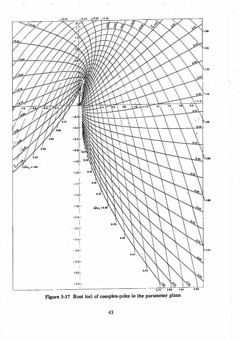
The characteristic equation (3.5.11 is a third-order equation. The proper root-set of this
equation can be achieved by employing the charts in figure 3-17 or figure 3-18. The
construction of the charts and their application in solving the pole placement problem for
the third-order digital control system are explained in detail in the following section.
The characteristic equation of closed loop system is given by:
42
Nu25
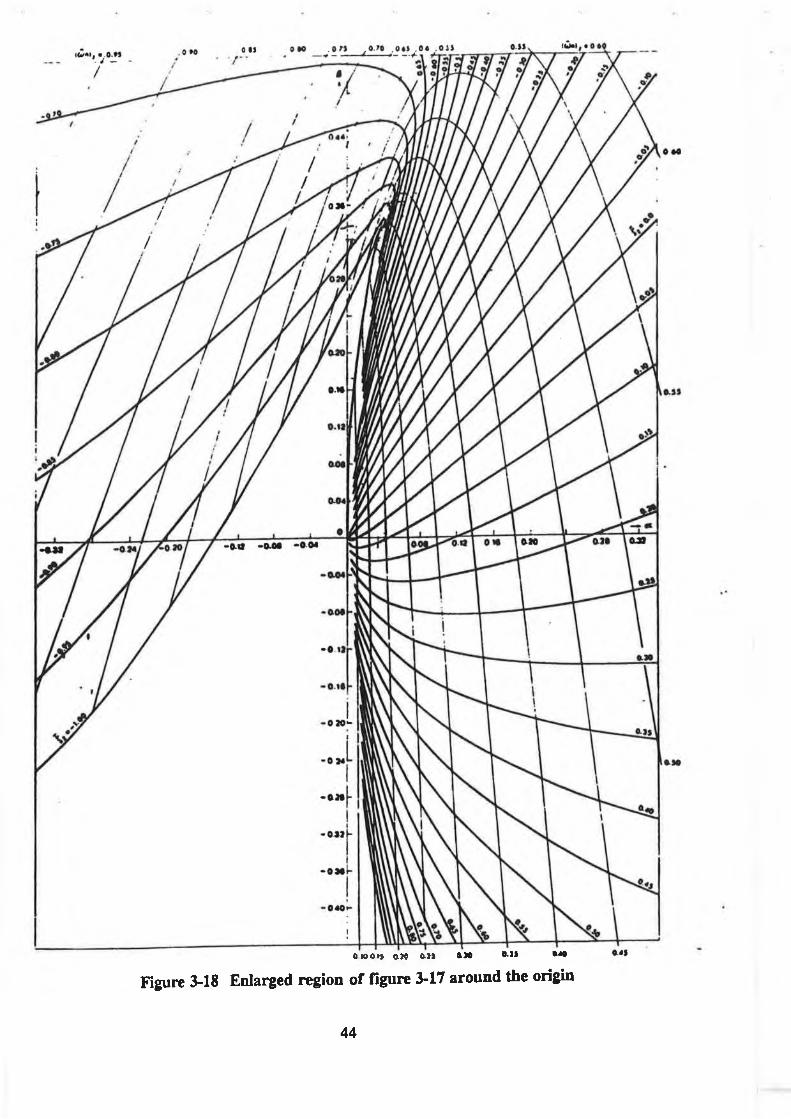
Figure 3-17 Root loci of complex-poles in the parameter plane
43
0 10 o t* AM a » O X 0.35 0 *
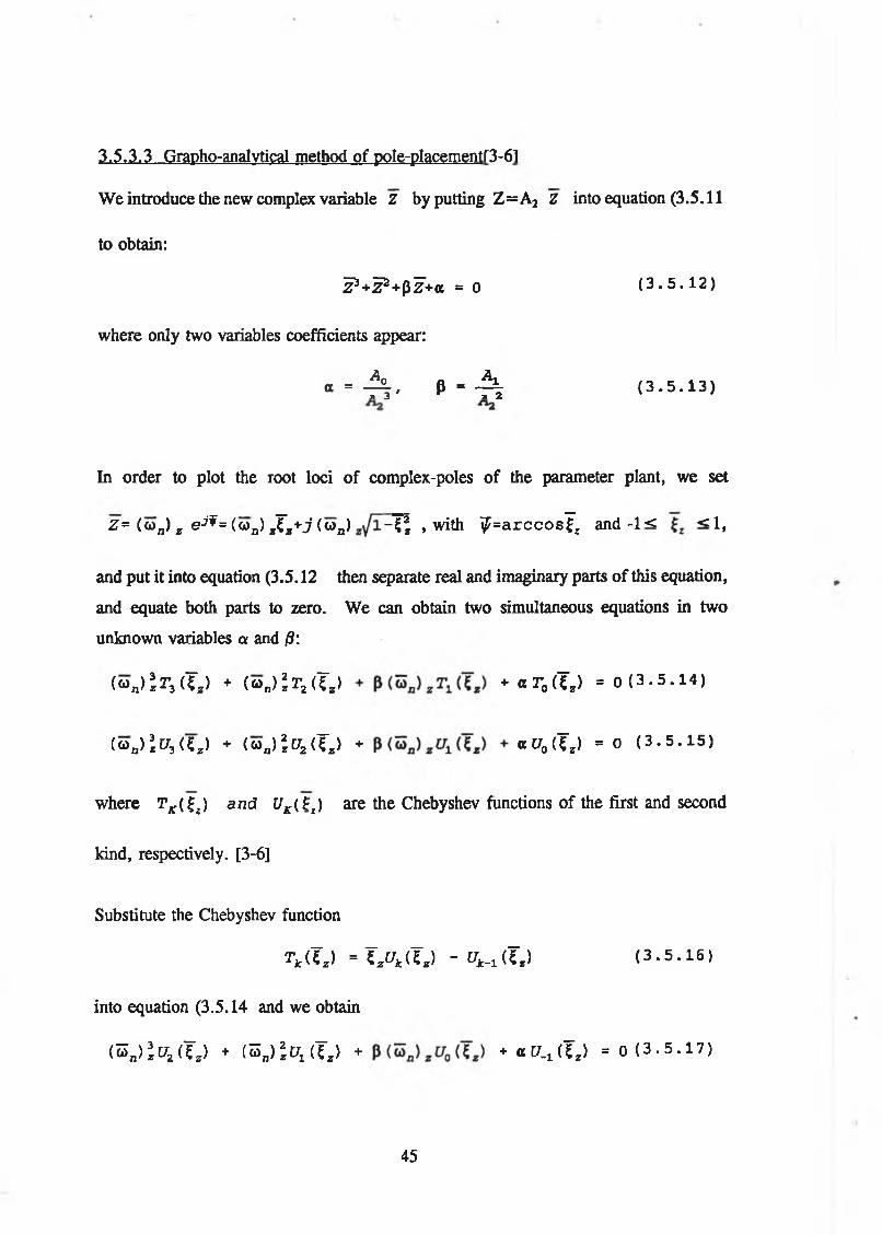
Figure 3-18 Enlarged region of figure 3-17 around the origin
44
We introduce the new complex variable Z by putting Z=A 2 Z into equation (3.5.11
to obtain:
?+ ]?+ p F + a = 0 ( 3 . 5 . 1 2 )
where only two variables coefficients appear:
a = A ' P = A ( 3 . 5 . 1 3 )
In order to plot the root loci of complex-poles of the parameter plant, we set
Z= (wn) a e j *= (wn) J B+j ( o n) -V z , with ^ = a rc c o s ? z and -1< < 1 ,
and put it into equation (3.5.12 then separate real and imaginary parts of this equation,
and equate both parts to zero. We can obtain two simultaneous equations in two
unknown variables a and 0:
<On>lr3(?,> * ( q J 1 t2(T2) n r , (?s) =0(3. 5 . 14)
( a j l u , a z ) * ( a „ ) 2, 0 2 (T,) * « c 0 (Tz) = 0 ( 3 . 5 . 1 5 )
where TK{tjz) and UK{I-Z) are the Chebyshev functions of the first and second
kind, respectively. [3-6]
Substitute the Chebyshev function
Tk a z) - T a ( T . ) - £ W ? , ) ( 3 . 5 . 1 6 )
into equation (3.5.14 and we obtain
(S„)J[/2 ( I 2) ♦ (S „ ) | t^ (T .) + < •« [ / . , ( I , ) = 0 ( 3 . 5 . 1 7 )
3.5.3.3 Grapho-analvtical method of pole-placementr3-61
45
Equations (3.5.15 and (3.5.17 can be solved easily for variable coefficients a and /3
to obtain:
« = ( w j z [(«„)*££(!*) +
( 3 . 5 . 1 8 )P = - ( » . > , [ ( « . ) . ! * < * , > + c i ( 5 . ) ]
where | | <1 and U* ( £z) , i/2* ( £z) , and t/3* (£z) are the Chebyshev
polynomials of the second kind[3-18] defined by
. — s in I k - a r c c o s f .) r;. ^ ) = '__________
Using equation (3.5.18 two families of curves with respect to different values of
= constant and ( u D) z = constant can be plotted as shown in figure 3-17.
Figure 3-18 shows the enlarged region of figure 3-17 around the origin. The curves in
figure 3-17 and figure 3-18 are in the (a,/3 that represent the loci of complex
poles of equation (3.5.12 as the parameters a and /3 vary. Using figure 3-16 and figure
3-17, we can easily use a pole placement technique for the third-order polynomials of
the feedback control system.
To relate the z-plane and the z -plane, we substitute
z = (<*>n) zZz + j ((oD) ¿¡l ~VZ and according to the relation z=A^z , we can
obtain :
(<*a) z = | A2\ ( u a) z ( 3 . 5 . 1 9 )
\ z = ( sgn(A2) ) l z ( 3 . 5 . 2 0 )
where equation (3.5.19 and (3.5.20 are the parameters defining the complex-pole
46
locations in the planes of the complex variables z and z
Since z=e,T, the parameters (&>„ and which determine the corresponding complex-
pole locations in the z-plane, can be obtained from the relative undamped natural
frequency 5>n and the damping coefficient f :
( o n) g = e"“n5T a n d \ z = cos ( u ^ t V i - Ç 2) ( 3 . 5 . 2 2 )
where, the Nyquist frequency band is:
Oso>n£ _ J L _ ( 3 . 5 . 2 3 )
Therefore, in the proposed procedure for the synthesizing controller parameters, it is
necessary first to specify the relative undamped natural frequency &>„ and the damping
coefficient f from the desired system characteristics with respect to the stability margin
and the speed of the continuous-time response. Then using equations (3.5.22 (3.5.19
and (3.5.20 the parameters “ and £ can be determined. Then the loci diagram
of pole-placement can be employed to find the intersection point of the curve
and (_„)z hence the respective parameters am and /3m can be obtained.
According to the Viète rule, the third real root of equation (3.5.12 can be calculated
from :
o z = - i - 2 l ( 3 . 5 . 2 4 )
The stability condition requires that all roots of equation (3.5.11 are inside the unit
circle; hence, we select A2, the absolute value of A2 must satisfy the constraints (&>„ < 1
and crt < 1,
47
or
l ^ k - J - r a n d \JL\< t J - . ■ ( 3 . 5 . 2 5 )
The other two coefficients A! and A in equation (3.5.11 can be obtained by using
equation (3.5.13
A* = p^Af an d A0 = a^Al ( 3 . 5 . 2 6 )
Putting the numerical values of A2, A1# A0 into equation (3.5.11 the parameter Kp, and
Kr can be obtained. KD can be adjusted later on.
3.5.3.4 Parameter calculation
From the design requirements, we know the damping coefficient ¿*=0.456 and the time
to peak t,,, is 20 msec. Using equation (3.5.27
t m = ---------------= 0 . 0 2 ( 3 . 5 . 2 7 )
we can obtain the undamped natural frequency:
con = 1 7 6 . 2 r a d / s e c ( 3 . 5 . 2 8 )
The Nyquist frequency band is specified by equation (3.5.23 and the respective value
is 0 < 176.2 <35300. From equation (3.5.22 the relationship between the „ and f
from the continuous-time response, and the parameters ( and determine
corresponding complex-pole locations in the z-plane which are readily obtained as
((*)*>* = e '° nCT = e"176,5x0,456x0,0001 = 0 . 992 and
Cz = COS(wn7 V l - i 2) = COS (176 . 2x0 . 0 0 0 1 ^ 1 -0 . 4 5 6 z) = 0 . 9 9 9 8 .
48
Meeting the stability condition &>„< 1 and az< 1, A2=-0.2945 can be selected. From
equation (3.5.19 and (3.5.20 we can obtain £z= -0 .9 9 9 8 and (~z)=0.34 .
Once iTz is determined, along the curve f"z = -0.9998=const of figure 3-16 or 3-17 the
point M(0.04,0.34 corresponding to the desired ( can be placed. The
coefficients and A, in equation (3.5.11 are obtained by using equation (3.5.13
A0 = am‘Al = 0 . 0 4 x ( - 2 . 9 5 4 ) 3 = - 1 . 0 2
Ai = P mAl = 0 . 3 4 x ( - 2 . 9 4 5 ) 2 = 2 . 9 4 8 8
Substituting the numerical values of A2, Aj and A« into (3.5.11 and solving equation
(3.5.11 for the controller parameters, we finally obtain
^ _ - \ - P 1 P 2 _ 1 . 0 2 - 0 . 9 7 4 _ n p K 0 . 0 0 1 8 6
_ A ir_ < P i +P 2 +P iP 2 > _ 2 . 9 4 8 8 - ( 1 + 0 . 9 4 7 + 1 x 0 . 9 4 7 ) _ Q 4 1 ~ K 0 . 0 0 1 8 6
The parameter KD has a small effect on the dynamic performance and it can be adjusted
in the practical controller later. The PID control algorithm can be rewritten by three
equations for DSP implementation.
e(kT0 = r(kT - c(kT
ut(kT = Kje(kT + u^Oc-l
u(kT = -KpC(kT - KD{c(kT - c[(k-l -I- ux(kT
where e(kT and ^(kT are the sample-data of the error signal and the output of the
cascade integral compensator, respectively.
49
3. Conclusion
This chapter has described two designs of a digital speed controller for a brushless servo
drive. First, we described the ‘analogue method of digital controller design’ using the
well-known analogue technologies in which the analogue controller with the traditional
PI implementation was converted into digital form which can be implemented by the
TMS320C30. This method makes the digital design become simple since we can
directly utilize the existing analogue controller. A more accurate design of a direct-
digital PID controller was also described. The method simplified the digital system into
a third-order digital feedback control system in which the controller parameters were
adjusted by using a graph-analytical method of pole-placement technique. Using this
method, the steady-state error of the system was eliminated and the controller parameters
were adjusted to give the desired accuracy, response speed, and stability margin of the
system, respectively. This controller has a faster response and greater accuracy than
the first traditional PI control but is more complex. The experimental results in chapter
7 show its advantages.
50
CHAPTER 4
SIMULATION OF BRUSHLESS SERVO SYSTEM
4.1 Introduction
In order to study the dynamic performance of the brushless servo system before a
practical test, a computer simulation scheme is used to model the prototype system.
This chapter introduces a simulation scheme for the brushless drive servo system, which
uses a block-oriented transfer function program written in the C langauge. Using this
scheme, we can examine the dynamical behaviour based on the system block diagram.
The brushless servo system can be described by a set of transform function blocks as
shown in figure 4-1 which is divided into two parts, the digital and the analogue part.
The digital part can be simulated easily, but the continuous part needs first to be
converted to a numerical form.
The continuous part can be represented by several blocks which may be one of the
following types:
( 1) I n t e g r a l : —s
K s + K( 2) P r o p o r t i o n a n d i n t e g r a l : — -----------
s( 3) I n e r t i a : ----- ——
T s + 1T, s + 1
( 4) F i r s t o r d e r l e a d o r l a g : K —±---------T, s + 1
51
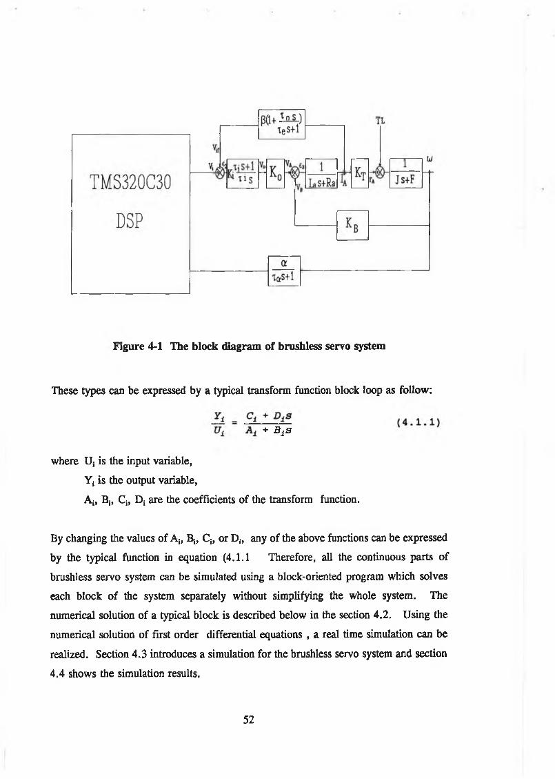
Figure 4-1 The block diagram of brushless servo system
These types can be expressed by a typical transform function block loop as follow:
+ Bj S
where Us is the input variable,
Yj is the output variable,
Aj, Bj, Cj, D; are the coefficients of the transform function.
By changing the values of Ah Bb Q, or Dj, any of the above functions can be expressed
by the typical function in equation (4.1.1 Therefore, all the continuous parts of
brushless servo system can be simulated using a block-oriented program which solves
each block of the system separately without simplifying the whole system. The
numerical solution of a typical block is described below in the section 4.2. Using the
numerical solution of first order differential equations , a real time simulation can be
realized. Section 4.3 introduces a simulation for the brushless servo system and section
4.4 shows the simulation results.
52

.2 The solution of tical block
Block (4.1.1 can be expressed as:
= ----- ------ ( C + Ds) = ( 4 . 2 . 1 )U ( s ) A + B s u ( s ) Z ( s )
where Z(s is an internal variable.
Equation (4.2.1 can be expressed separately by follows:
Z ( s ) = 1U(s) A + B s
( 4 . 2 . 2 )
= C + D s ( 4 . 2 . 3 )Z ( s )
Equation (4.2.2 and (4.2.3 can be expressed in the time domain as:
A Z ( t ) + B dZ} P ~ = U ( t ) ( 4 . 2 . 4 )a t
C Z ( t ) + D-dZ^ ]- = Y ( t ) ( 4 . 2 . 5 )arc
In order to obtain the time-domain solution, we convert equation (4.2.4 into:
4 ? ( = - — z ( t ) + ( 4 . 2 . 6 )dC B B
It should be noted that the denominator B can not be zero, this means the typical block
(4.1.1 must always include an integral term. Substituting equation (4.2.6 into (4.2.5
we have:
53
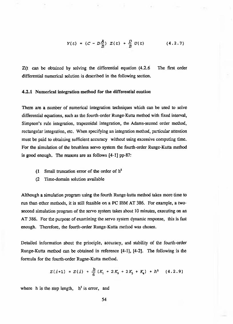
y(t) = (c - d 4 ) z ( t ) + % u( t ) ( 4 . 2 . 7 )
Z(t can be obtained by solving the differential equation (4.2.6 The first order
differential numerical solution is described in the following section.
4.2.1 Numerical integration method for the differential euation
There are a number of numerical integration techniques which can be used to solve
differential equations, such as the fourth-order Runge-Kutta method with fixed interval,
Simpson’s rule integration, trapezoidal integration, the Adams-second order method,
rectangular integration, etc. When specifying an integration method, particular attention
must be paid to obtaining sufficient accuracy without using excessive computing time.
For the simulation of the brushless servo system the fourth-order Runge-Kutta method
is good enough. The reasons are as follows [4-1] pp-87:
(1 Small truncation error of the order of h5
(2 Time-domain solution available
Although a simulation program using the fourth Runge-kutta method takes more time to
run than other methods, it is still feasible on a PC IBM AT 386. For example, a two-
second simulation program of the servo system takes about 10 minutes, executing on an
AT 386. For the purpose of examining the servo system dynamic response, this is fast
enough. Therefore, the fourth-order Runge-Kutta method was chosen.
Detailed information about the principle, accuracy, and stability of the fourth-order
Runge-Kutta method can be obtained in reference [4-1], [4-2]. The following is the
formula for the fourth-order Rugne-Kutta method.
Z ( i + 1 ) = Z ( i ) + -^ ( j q + 2 JC, + 2 K3 + JQ) + h 5 ( 4 . 2 . 9 )6
where h is the step length, h5 is error, and
54
Kx = MZ± + NUi ( 4 . 2 . 1 0 )
JC, = M{ Z± + ^ h k x) + NUiZ
( 4 . 2 . 1 1 )
K3 = M( Z1 + \ h K 2) + NUi ( 4 . 2 . 1 2 )
Kt = M{ Zi + * £ , ) + NU1 ( 4 . 2 . 1 3 )
.3 siulation rogra
In general, for a complex single input and single output system, the mathmetical model
needslo be simplified into a high order differential equation:
J r ( t > * * ........ * a ^ - f c y ( t ) * v < « 3
a _ 1 . _ d B~2 d * *
= + C2 - ^ i U ( t ) + + Cn - l ~ § i U ^ + C-a U ( t )
where y(t is the output of system
u(t is the input of system
This simplification often ignores some functions in the system, which effects the
accuracy of the simulation. Here we introduce a block-oriented transfer-function
program which employs the typical loop and proportional gain to complete the system
block diagram. Therefore, we do not need to simplify the total transfer function of the
system.
4.3.1 Simulation of the continuous part of the brushless servo system
The brushless servo system, shown in figure 4-1, has several blocks each of which can
be represented by the typical block or a gain. For example, the current loop is a
55
proportional and integral loop which is expressed by Ki~ ^ — and theT , S
T s+1
parameters of the typical block for this is A2=0, B ^ T ;, C ^ K ;, D2=KiTi. The
proportion loop of the inverter can be expressed as the gain Kq.
Obviously, each block of the system is a transfer function which can be expressed by
changing the parameters of the typical block. The program is written according to the
system block diagram as shown in figure 3-5. The output of the previous loop is the
input of the next loop. At the summing junction, the difference of outputs of two loops
becomes the input to the next loop. The program for the continuous control part of the
brushless dc servo system is presented in Appendix 1. The Runge-Kutta step h of the
continuous-domain parts must be selected short enough to minimize the delay.
Normally it should be more than a hundred times smaller than the sampling interval of
the digital controller.
4.3.2 The simulation of the digital controller
The digital controller designs have been described in the previous chapter. For design
I, we utilize equation (3.3.37 where the sampling period T=100 /xsec, KP=9.39, and
Kt= 0.99335. The simulation program is presented in Appendix 2 in which an input
command of 5 (volt represents a motor speed of 5000 rpm.
In design n , we use equation (3.4.1 which can be rewritten as three equations for the
simulation.
e ( k T ) = r { k T ) - c ( k T )
^ ( k T ) = K j e ( k T ) + u 1[(*r- l ) ] ( 4 . 3 . 2 )
u ( k T ) = - K pc ( k F ) - KD{ B { k r ) - b [ ( k - 1 ) T\ } +u1 ( k l i)
where e(kT and ^(kT represent the sample-data of the error signal and the output of
the cascade integral compensator, respectively. The program for design II, presented
in Appendix 3, has controller parameters which are selected as: sampling period T =
56
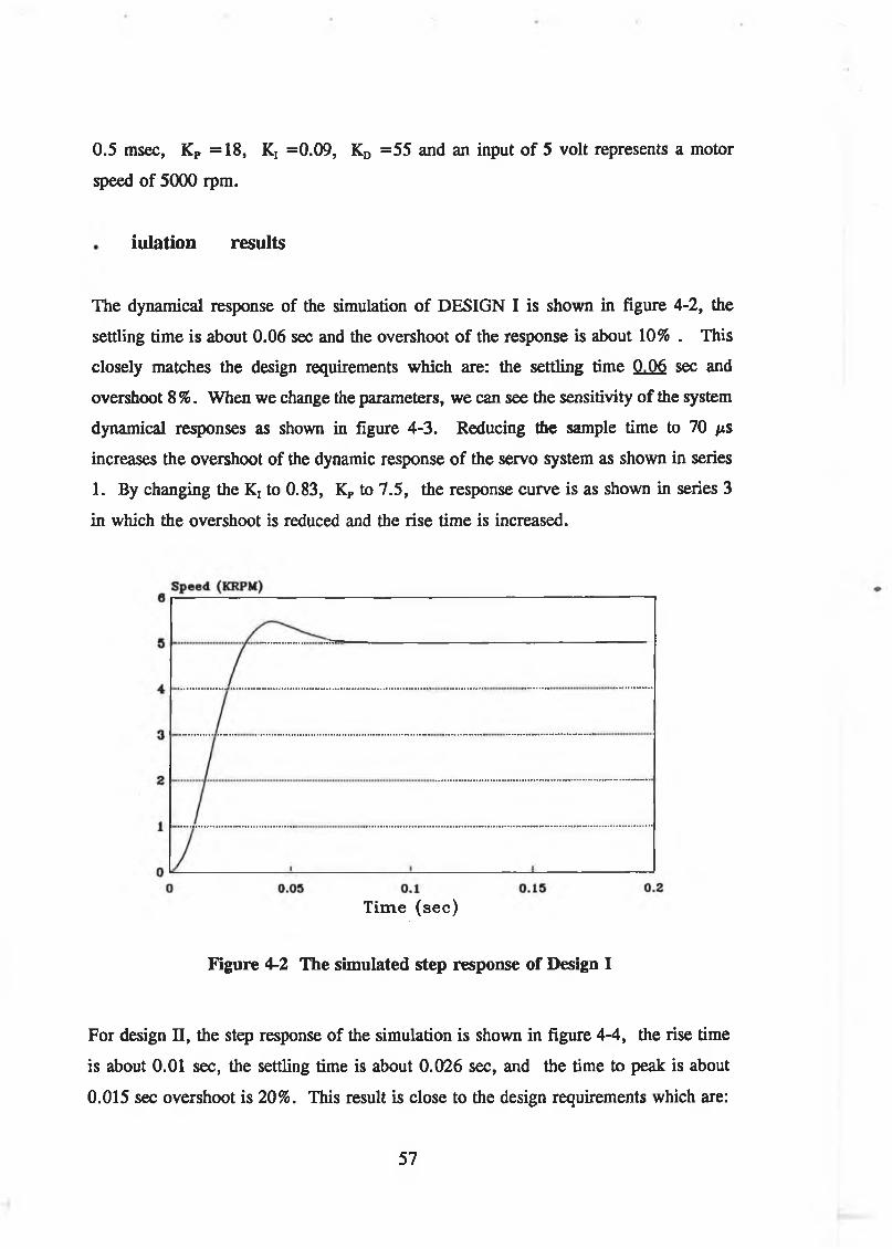
0.5 msec, KP =18, Kt =0.09, KD =55 and an input of 5 volt represents a motor
speed of 5000 rpm.
iulation results
The dynamical response of the simulation of DESIGN I is shown in figure 4-2, the
settling time is about 0.06 sec and the overshoot of the response is about 10% . This
closely matches the design requirements which are: the settling time 0.06 sec and
overshoot 8 %. When we change the parameters, we can see the sensitivity of the system
dynamical responses as shown in figure 4-3. Reducing the sample time to 70 fis
increases the overshoot of the dynamic response of the servo system as shown in series
1. By changing the Kj to 0.83, KP to7.5, the response curve is as shown in series 3
in which the overshoot is reduced and the rise time is increased.
Tim e (sec)
Figure 4-2 The simulated step response of Design I
For design n , the step response of the simulation is shown in figure 4-4, the rise time
is about 0.01 sec, the settling time is about 0.026 sec, and the time to peak is about
0.015 sec overshoot is 20%. This result is close to the design requirements which are:
57
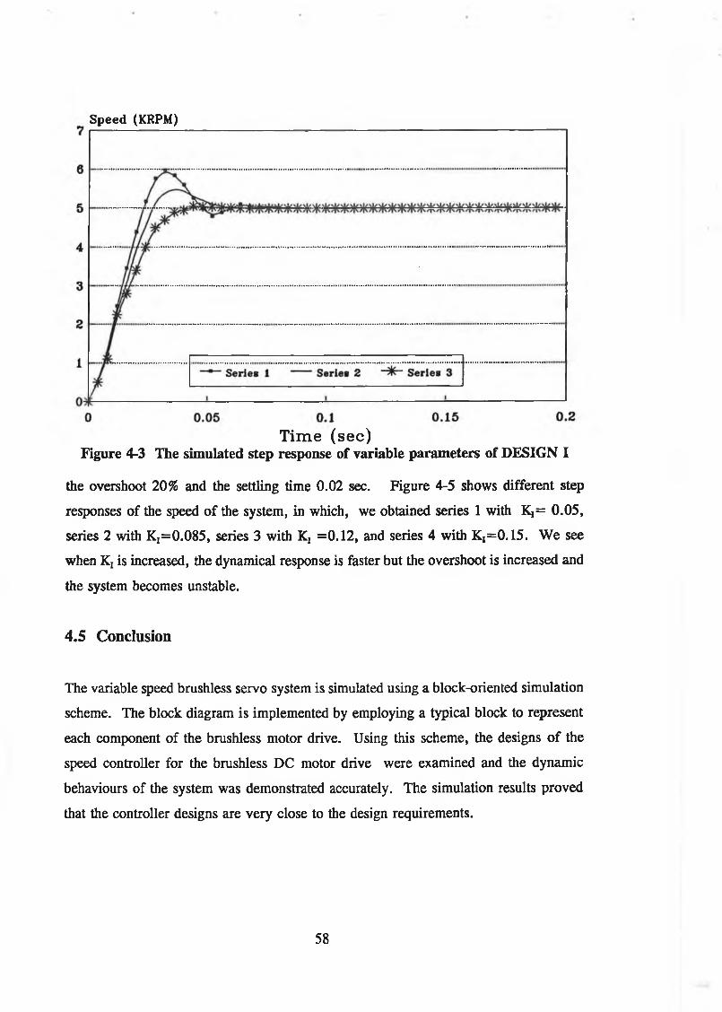
Speed (KRPM)
T im e ( s e c )Figure 4-3 The simulated step response of variable parameters of DESIGN I
the overshoot 20% and the settling time 0.02 sec. Figure 4-5 shows different step
responses of the speed of the system, in which, we obtained series 1 with KI= 0.05,
series 2 with 1^=0.085, series 3 with Kj =0.12, and series 4 with K j=0,15. We see
when Kj is increased, the dynamical response is faster but the overshoot is increased and
the system becomes unstable.
4.5 Conclusion
The variable speed brushless servo system is simulated using a block-oriented simulation
scheme. The block diagram is implemented by employing a typical block to represent
each component of the brushless motor drive. Using this scheme, the designs of the
speed controller for the brushless DC motor drive were examined and the dynamic
behaviours of the system was demonstrated accurately. The simulation results proved
that the controller designs are very close to the design requirements.
58
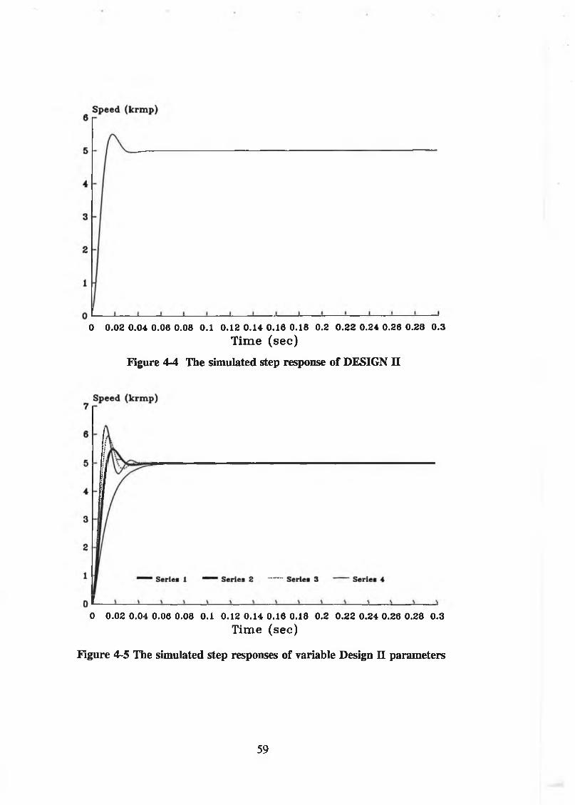
0 0 . 0 2 0 . 0 4 0 . 0 6 0 . 0 8 0 . 1 0 . 1 2 0 . 1 4 0 . 1 6 0 . 1 8 0 . 2 0 . 2 2 0 . 2 4 0 . 2 6 0 . 2 8 0 . 3
Tim e (s e c )
Figure 4-4 The simulated step response of DESIGN II
0 0 . 0 2 0 . 0 4 0 . 0 6 0 . 0 8 0 . 1 0 . 1 2 0 . 1 4 0 . 1 6 0 . 1 8 0 . 2 0 . 2 2 0 . 2 4 0 . 2 6 0 . 2 8 0 . 3
Time (se c )
Figure 4-5 The simulated step responses of variable Design n parameters
59
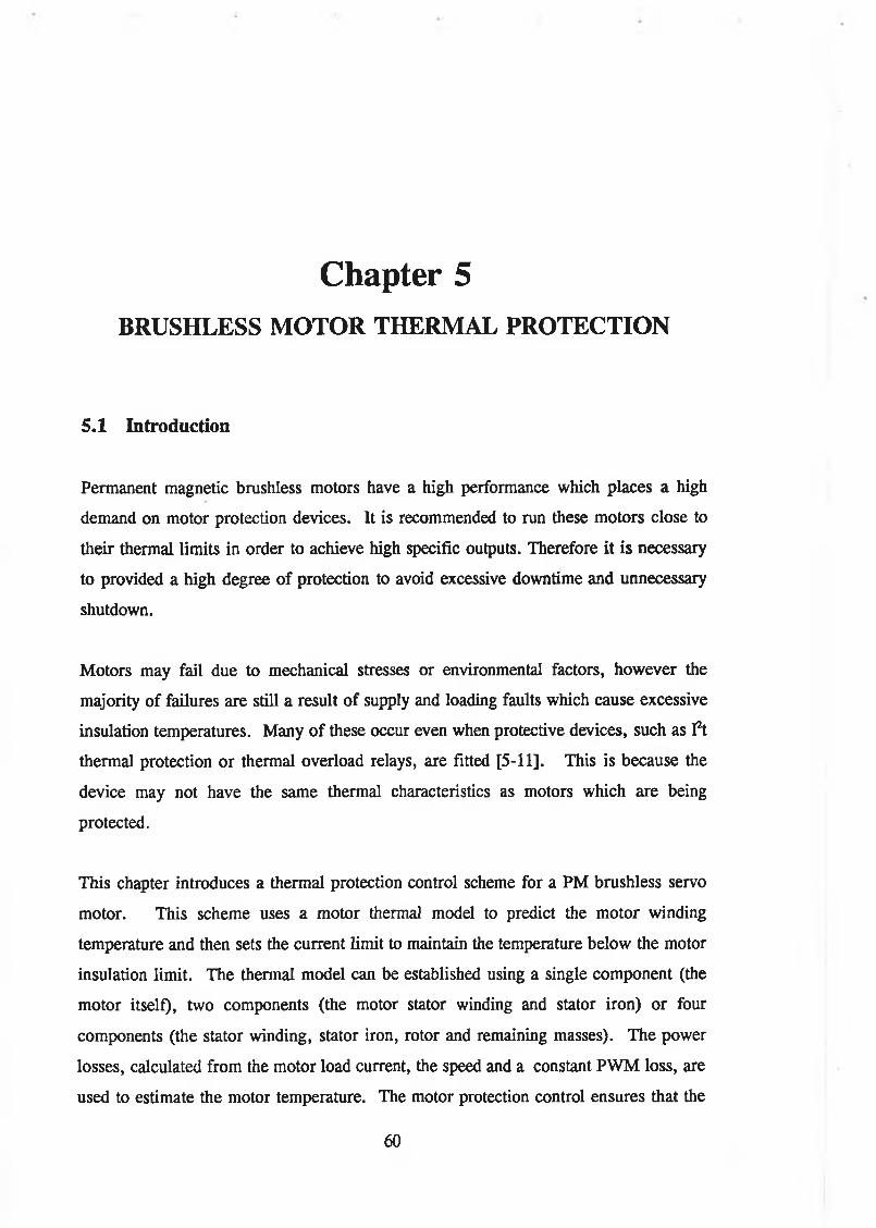
Chapter 5BRUSHLESS M OTOR THERMAL PROTECTION
5.1 Introduction
Permanent magnetic brushless motors have a high performance which places a high
demand on motor protection devices. It is recommended to run these motors close to
their thermal limits in order to achieve high specific outputs. Therefore it is necessary
to provided a high degree of protection to avoid excessive downtime and unnecessary
shutdown.
Motors may fail due to mechanical stresses or environmental factors, however the
majority of failures are still a result of supply and loading faults which cause excessive
insulation temperatures. Many of these occur even when protective devices, such as f t
thermal protection or thermal overload relays, are fitted [5-11]. This is because the
device may not have the same thermal characteristics as motors which are being
protected.
This chapter introduces a thermal protection control scheme for a PM brushless servo
motor. This scheme uses a motor thermal model to predict the motor winding
temperature and then sets the current limit to maintain the temperature below the motor
insulation limit. The thermal model can be established using a single component (the
motor itself), two components (the motor stator winding and stator iron) or four
components (the stator winding, stator iron, rotor and remaining masses). The power
losses, calculated from the motor load current, the speed and a constant PWM loss, are
used to estimate the motor temperature. The motor protection control ensures that the
60
motor stator winding temperature always remains below the insulation class limit. This
provides a maximum utilization of the motor output power during transient loads.
The brushless motor power losses are described in section 5.2, they can be subdivided
into copper losses, core losses, windage losses, and mechanical losses. Then section 5.3
introduces a single-component thermal simulation which is established using an electrical
R-C analogue and is used to predict the temperature of the motor. Section 5.4 describes
a two-component simulation. Section 5.6 describes the thermal protection control
procedure. Finally, section 5.7 introduces a simulation of this procedure for an AEG
BHT 2214M brushless motor. Using this scheme, the motor thermal capacity can be
utilized more efficiently and can drive loads exceeding its continuous rating for short
periods of time.
5.2 Power loss
The heat generated within the motor is a result of electrical and internal power losses
which include:
1 Copper loss :
This is the Joule heat, PR. in the armature resistance which is expressed as:
Pc = I 2 x Ra ( 5 . 2 . 1 )
where I is the equivalent DC armature current.
Rt is the equivalent DC resistance.
2 Windage loss:
The work required for the rotor to move through the air. This is converted to heat
inside the rotor and in the air.
3 Mechanical loss:
This is caused by friction.
61
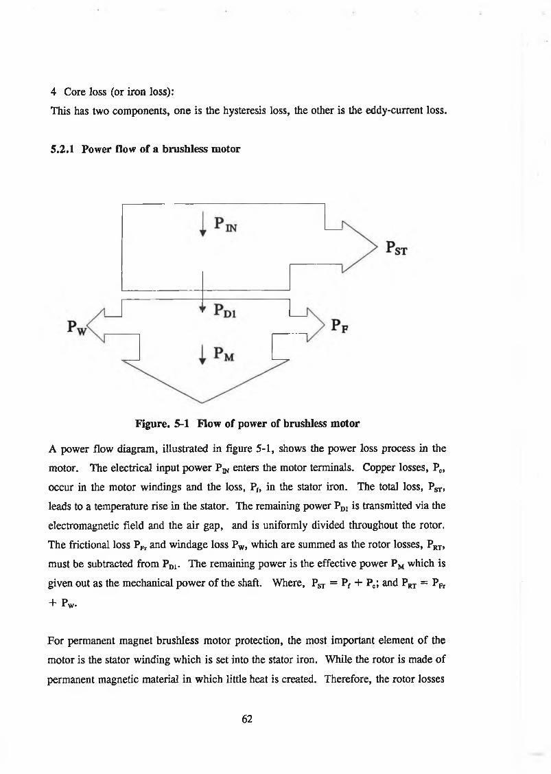
4 Core loss (or iron loss):
This has two components, one is the hysteresis loss, the other is the eddy-current loss.
5.2.1 Power flow of a brushless motor
Figure. 5-1 Flow of power of brushless motor
A power flow diagram, illustrated in figure 5-1, shows the power loss process in the
motor. The electrical input power P ^ enters the motor terminals. Copper losses, Pc,
occur in the motor windings and the loss, Pf, in the stator iron. The total loss, F * s t >
leads to a temperature rise in the stator. The remaining power PDI is transmitted via the
electromagnetic field and the air gap, and is uniformly divided throughout the rotor.
The frictional loss PFr and windage loss Pw, which are summed as the rotor losses, PRT,
must be subtracted from PD1. The remaining power is the effective power PM which is
given out as the mechanical power of the shaft. Where, PST = Pf + Pc; and PRT = PFr
+ Pw.
For permanent magnet brushless motor protection, the most important element of the
motor is the stator winding which is set into the stator iron. While the rotor is made of
permanent magnetic material in which little heat is created. Therefore, the rotor losses
62
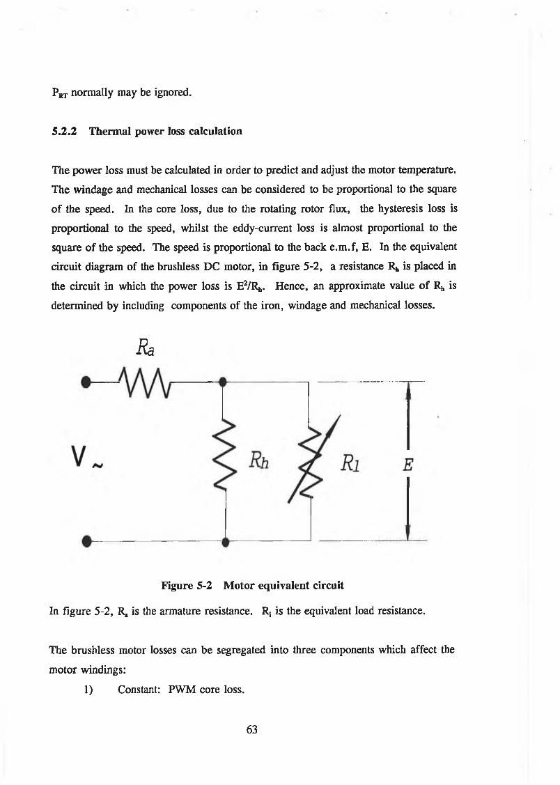
PRX normally may be ignored.
5.2.2 Thermal power loss calculation
The power loss must be calculated in order to predict and adjust the motor temperature.
The windage and mechanical losses can be considered to be proportional to the square
of the speed. In the core loss, due to the rotating rotor flux, the hysteresis loss is
proportional to the speed, whilst the eddy-current loss is almost proportional to the
square of the speed. The speed is proportional to the back e.m.f, E. In the equivalent
circuit diagram of the brushless DC motor, in figure 5-2, a resistance Rj, is placed in
the circuit in which the power loss is E2/!^. Hence, an approximate value of Rh is
determined by including components of the iron, windage and mechanical losses.
Ra
Figure 5-2 Motor equivalent circuit
In figure 5-2, Ra is the armature resistance. R, is the equivalent load resistance.
The brushless motor losses can be segregated into three components which affect the
motor windings:
1) Constant: PWM core loss.
63
2) Proportional to o>2 : E2/Rh including core loss, friction loss and windage
loss.
3) Proportional to I2R, : copper losses.
The losses (1) and (2), denoted Pf, cause heat in the motor stator iron. The rotor loss PRT
is small and can be included in Pf. The loss (3) is Pc which creates heat in stator
windings. Pf can be expressed as:
Pf = K0 + ( 5 . 2 . 2 )
and Pc is:
Pc = I 2 x Ra ( 5 . 2 . 3 )
The total thermal power loss of a brushless motor can be calculated from:
P i o s s = p f + P C = K o + - r r + ( 5 . 2 . 4 )Kh
where Plos, is the total motor power loss.
Ko is a constant representing the PWM loss.
E is the back e.m.f.
R,, is the equivalent resistance of loss (2).
I. is the equivalent DC current.
R, is the equivalent DC armature resistance.
5.2.3 Maximum allowable power loss
In order to set the limit for the highest allowable motor temperature, we need to
calculate the maximum allowable power loss. The speed-torque limits of a permanent
magnet brushless motor are shown in figure 5-3.
64
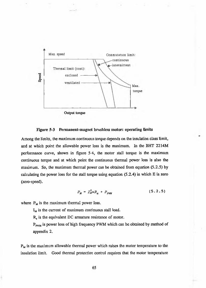
Max. speed Comm utation lim it:
Figure 5-3 Permanent-magnet brushless motor: operating limits
Among the limits, the maximum continuous torque depends on the insulation class limit,
and at which point the allowable power loss is the maximum. In the BHT 2214M
performance curve, shown in figure 5-4, the motor stall torque is the maximum
continuous torque and at which point the continuous thermal power loss is also the
maximum. So, the maximum thermal power can be obtained from equation (5.2.5) by
calculating the power loss for the stall torque using equation (5.2.4) in which E is zero
(zero-speed).
PM = I 2MxRa + Ppm ( 5 . 2 . 5 )
where PM is the maximum thermal power loss.
IM is the current of maximum continuous stall load.
R, is the equivalent DC armature resistance of motor.
PpwM is power loss of high frequency PWM which can be obtained by method of
appendix 2.
PM is the maximum allowable thermal power which raises the motor temperature to the
insulation limit. Good thermal protection control requires that the motor temperature
65
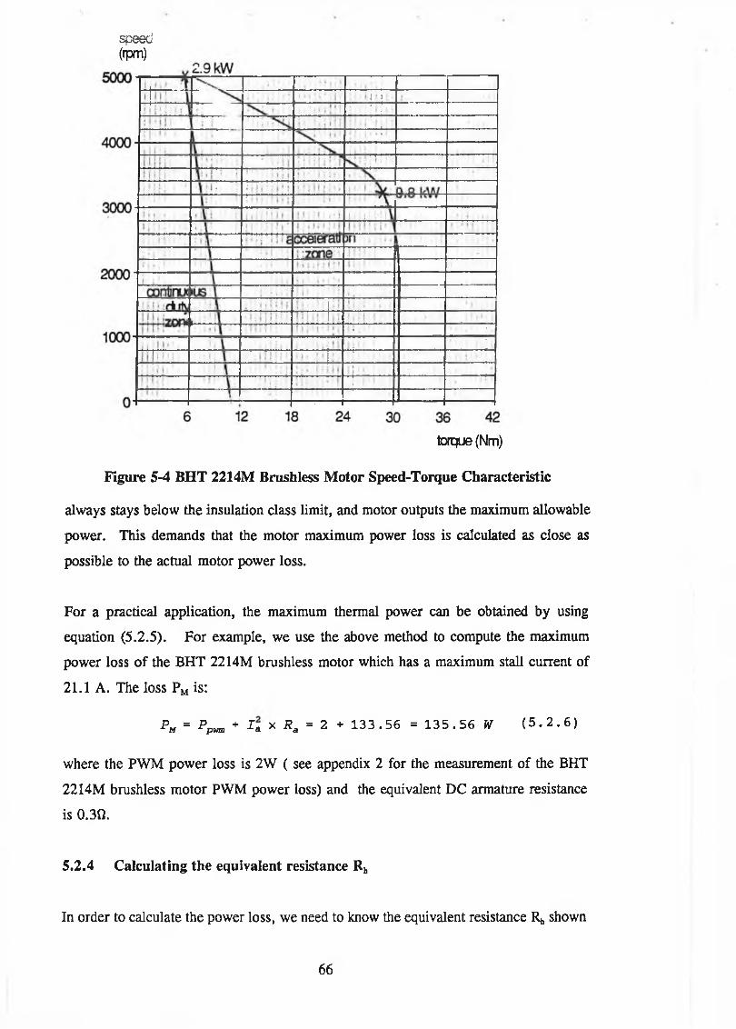
speed(rpm)
torque (Nm)
Figure 5-4 BHT 2214M Brushless Motor Speed-Torque Characteristic
always stays below the insulation class limit, and motor outputs the maximum allowable
power. This demands that the motor maximum power loss is calculated as close as
possible to the actual motor power loss.
For a practical application, the maximum thermal power can be obtained by using
equation (5.2.5). For example, we use the above method to compute the maximum
power loss of the BHT 2214M brushless motor which has a maximum stall current of
21.1 A. The loss PM is:
P M = Ppwm + J a x R a = 2 + 1 3 3 . 5 6 = 1 3 5 . 5 6 W ( 5 . 2 . 6 )
where the PWM power loss is 2W ( see appendix 2 for the measurement of the BHT
2214M brushless motor PWM power loss) and the equivalent DC armature resistance
is 0.30.
5.2.4 Calculating the equivalent resistance Rh
In order to calculate the power loss, we need to know the equivalent resistance Rh shown
6 6
in figure 5-2. This can be calculated from the motor continuous duty speed-torque
curve. A maximum power loss point can also be found on this curve at the motor
maximum speed. The power loss at this point is approximately equal to that at the
maximum stall torque. Hence, Rj, can be obtained:
R b = --------------------------- ( 5 . 2 . 7 )~ Ppm
where Pm is the maximum power loss.
I, is the current at the point of the maximum output power.
E is the back e.m.f at the point of the maximum output power, which can be
derived from speed/Kb (back E.M.F constant).
R, is the equivalent DC armature resistance of motor.
For the AEG BHT 2214M brushless motor, at the point of the maximum power output,
the speed is 5000 rpm and the torque is 5.2 Nm. The current, therefore, is torque/Kx
= 5.2/0.536=9.7 A. The back e.m.f, E=speed*Kb=5000*0.056=280 V. According
to equation (5.2.7), Rh is:
R h = — = ---------------2 8 ° 2-------------- * 748QP f i - P p » n - j 2 * a 1 3 5 . 5 6 - 2 - 9 . 72x 0 . 3
5.2.5 Drawing the maximum continuous Speed-Torque characteristic curve
In order to continuously obtain the maximum allowable output power during variable
speeds and transient loads, we need to draw the maximum continuous speed-torque
characteristic curve as the output power limit. PM, the maximum continuous thermal
loss, the power loss in equation (5.2.4), has the form of the parametric equation for an
ellipse. Using this equation, the continuous speed-torque curve is drawn as an elliptic
shaped curve to set motor maximum allowable current limits (Normally the continuous
speed-torque characteristic curve is drawn by an oblique line linking both the maximum
power output point and the stall point). This curve can be drawn using the following
steps:
67
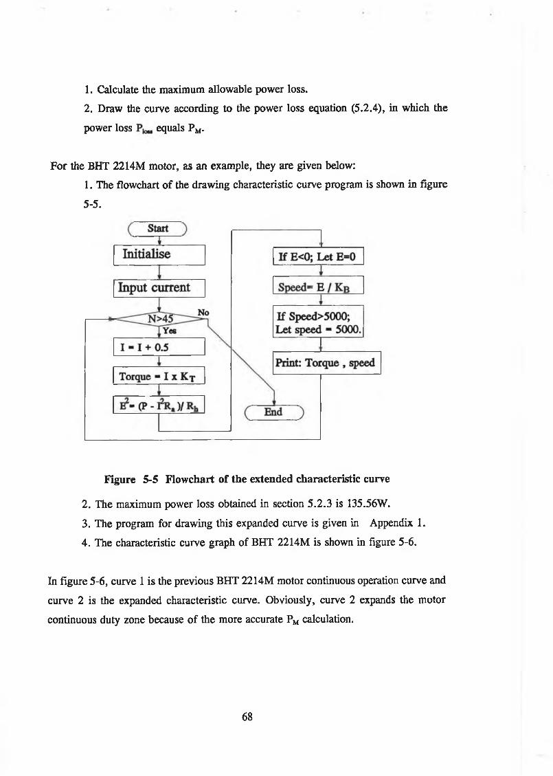
1. Calculate the maximum allowable power loss.
2. Draw the curve according to the power loss equation (5.2.4), in which the
power loss equals PM.
For the BHT 2214M motor, as an example, they are given below:
1. The flowchart of the drawing characteristic curve program is shown in figure
5-5.
Figure 5-5 Flowchart of the extended characteristic curve
2. The maximum power loss obtained in section 5.2.3 is 135.56W.
3. The program for drawing this expanded curve is given in Appendix 1.
4. The characteristic curve graph of BHT 2214M is shown in figure 5-6.
In figure 5-6, curve 1 is the previous BHT 2214M motor continuous operation curve and
curve 2 is the expanded characteristic curve. Obviously, curve 2 expands the motor
continuous duty zone because of the more accurate PM calculation.
68
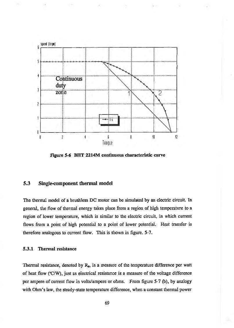
T o u q u e
Figure 5-6 BHT 2214M continuous characteristic curve
5.3 Single-component thermal model
The thermal model of a brushless DC motor can be simulated by an electric circuit. In
general, the flow of thermal energy takes place from a region of high temperature to a
region of lower temperature, which is similar to the electric circuit, in which current
flows from a point of high potential to a point of lower potential. Heat transfer is
therefore analogous to current flow. This is shown in figure. 5-7.
5.3.1 Thermal resistance
Thermal resistance, denoted by R*, is a measure of the temperature difference per watt
of heat flow (°C/W), just as electrical resistance is a measure of the voltage difference
per ampere of current flow in volts/ampere or ohms. From figure 5-7 (b), by analogy
with Ohm’s law, the steady-state temperature difference, when a constant thermal power
69
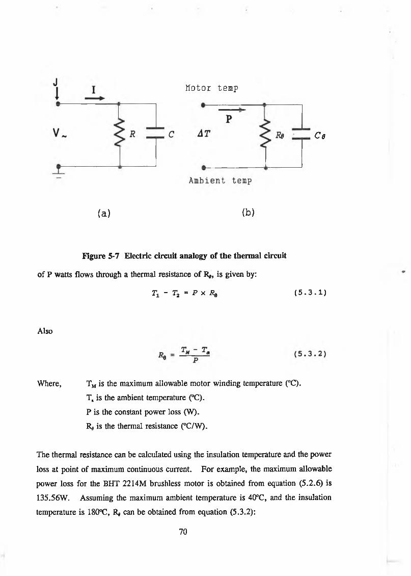
Motor temp
Ce
(a) (b)
Figure 5-7 Electric circuit analogy of the thermal circuit
of P watts flows through a thermal resistance of R*, is given by:
Ti ~ T2 = p x Re ( 5 . 3 . 1 )
Also
Where, TM is the maximum allowable motor winding temperature (°C).
T, is the ambient temperature (°C).
P is the constant power loss (W).
R* is the thermal resistance (°C/W).
The thermal resistance can be calculated using the insulation temperature and the power
loss at point of maximum continuous current. For example, the maximum allowable
power loss for the BHT 2214M brushless motor is obtained from equation (5.2.6) is
135.56W. Assuming the maximum ambient temperature is 40°C, and the insulation
temperature is 180°C, R# can be obtained from equation (5.3.2):
70
5.3.2 Thermal capacitance
For transient conditions, the motor thermal storage capacity should be taken into
consideration in order to calculate the motor winding temperature. Thermal capacity is
the heat energy stored per degree of the temperature rise. When the motor temperature
rises rapidly on overcurrents, the thermal capacity can be utilized to give a significant
short term overcurrent capability and thereby avoid an unduly conservative design.
Thermal capacity is analogous to capacitance in the electrical circuit as shown in the
figure 5-7. The thermal capacitance C s can be determined by the thermal time constant
Tfo.
J?e x Ce = ; A l s o Ce = ( 5 . 3 . 3 )
where we assume the thermal resistance R is a constant.
5.3.3 Thermal equation
The motor transient thermal behaviour can be modeled approximately by an R-C
network, shown in figure 5-7 (b). Assume a constant heating power P, is suddenly
applied to the motor at zero time. For this step input in heating power, there is a
corresponding step input of current in the electrical analog of figure 5-7 (a). This
current must charge up the network capacitance before a voltage can appear at input
terminal J. Consequently, there is a delay in the build up of voltage at the input
terminals. Similarly, there is a time lag in the decay of winding temperature when the
input P is removed. For an electrical RC network in figure 5-7 (a), the voltage
equation is:
71
d tV = I R - R C
A corresponding thermal equation can be obtained as:
T , -T . - PR, - X , C, ( 5 . 3 . 4 )
where Tm is the motor temperature.
T, is the ambient temperature.
P is the thermal power.
AT is the temperature difference,
t is the time variable.
C 9 is the thermal capacitance.
R* is the thermal resistance.
For real time motor temperature prediction, equation (5.3.4) must be transformed to a
digital form. The Laplace transform of equation (5.3.4) is:
T ( S ) = P ( s ) R t - T ^ T i s ) S ( 5 . 3 . 5 )
where T(S) is the difference of Tm - T,.
Tfc is the thermal time constant which is equal to R*C#.
Also,
T ( s ) _ ^6P ( s ) s + 1
( 5 . 3 . 6 )
The z transform of equation (5.3.6) can be expressed as:
T ( k ) _ b z -1 P ( k ) i - a z ' 1
-ka = e Tth
-k
¿> = Rg a - e Ttb)
( 5 . 3 . 7 )
72
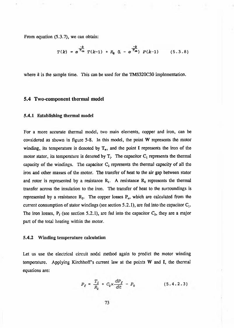
-k -kT ( k ) = e Ttb T ( k - l ) + i?e a - e Tth) P ( k - l ) ( 5 . 3 . 8 )
where k is the sample time. This can be used for the TMS320C30 implementation.
5.4 Two-component thermal model
5.4.1 Establishing thermal model
For a more accurate thermal model, two main elements, copper and iron, can be
considered as shown in figure 5-8. In this model, the point W represents the motor
winding, its temperature is denoted by Tw, and the point I represents the iron of the
motor stator, its temperature is denoted by T;. The capacitor represents the thermal
capacity of the windings. The capacitor Q represents the thermal capacity of all the
iron and other masses of the motor. The transfer of heat to the air gap between stator
and rotor is represented by a resistance Rj. A resistance Ro represents the thermal
transfer across the insulation to the iron. The transfer of heat to the surroundings is
represented by a resistance R2. The copper losses Pc, which are calculated from the
current consumption of stator windings (see section 5.2.1), are fed into the capacitor Q.
The iron losses, Pf (see section 5.2.1), are fed into the capacitor C2, they are a major
part of the total heating within the motor.
5.4.2 Winding temperature calculation
Let us use the electrical circuit nodal method again to predict the motor winding
temperature. Applying Kirchhoffs current law at the points W and I, the thermal
equations are:
From equation (5.3.7), we can obtain:
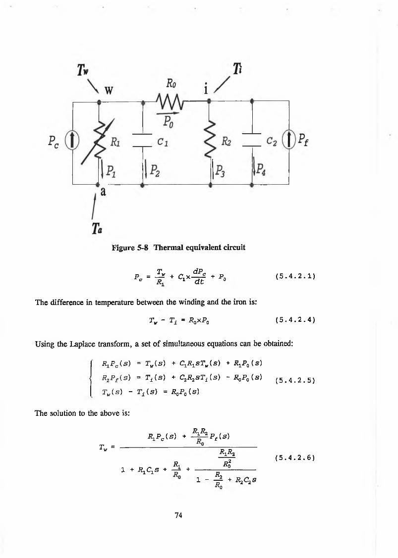
Figure 5-8 Thermal equivalent circuit
T dPp = —a + c x c + p Pc R. Cl d t
( 5 . 4 . 2 . 1 )
The difference in temperature between the winding and the iron is:
Tw ~ — R0xPq ( 5 . 4 . 2 . 4 )
Using the Laplace transform, a set of simultaneous equations can be obtained:
i?xPc (s) = Tw( s ) + C ^ s T j s ) + RxP0 ( s )
R2Pf ( s ) = T1 (.s) + C2R2s T1 {s ) - R0P0 ( s ) ( 5 . 4 . 2 . 5 )
Tw( s ) - ( s ) = R0P0 (s)
The solution to the above is:
, , R, R- RxPc ( s ) + - ± ± P t {s)
T =■L w
R,1 + R1C13 + - i +
• 1 ^ 2
rI
i - ^ + r 2c 2s
( 5 . 4 . 2 . 6 )
74
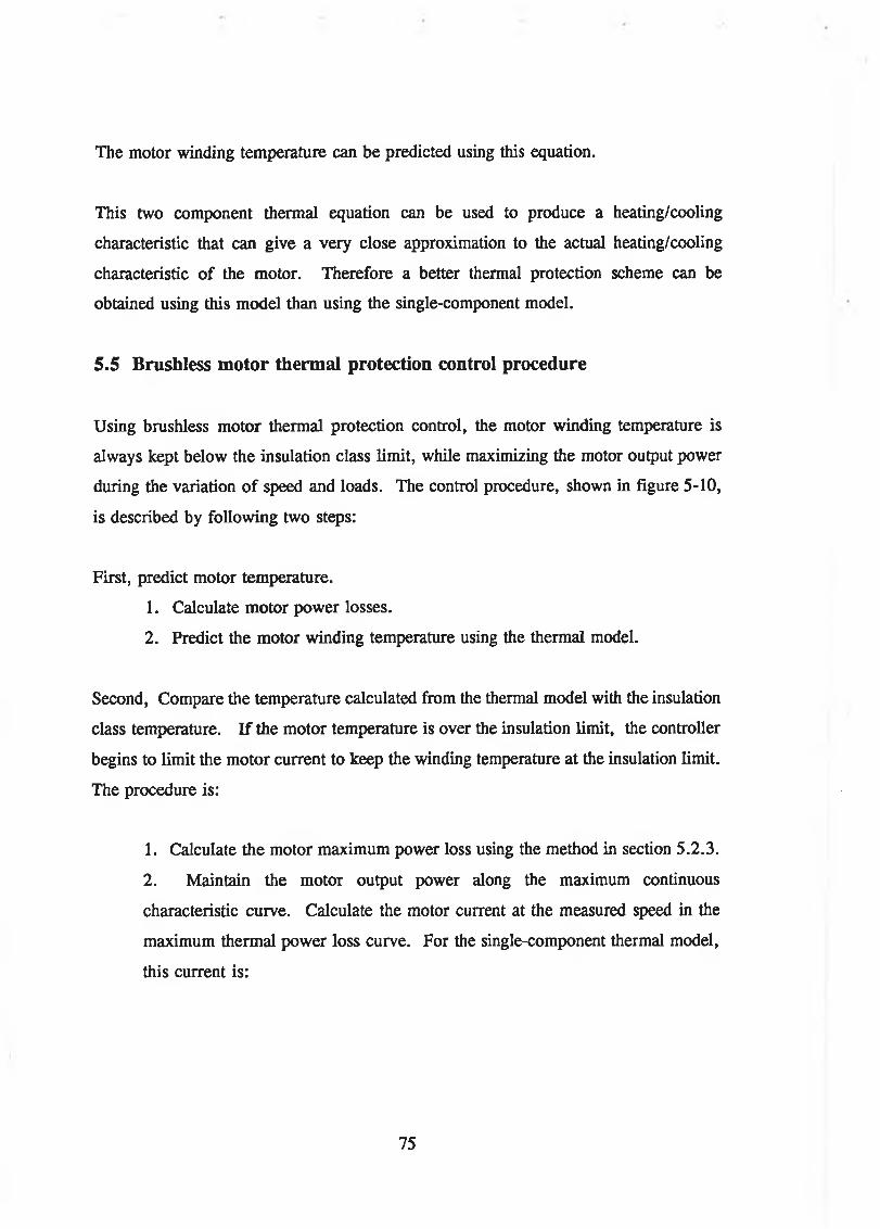
The motor winding temperature can be predicted using this equation.
This two component thermal equation can be used to produce a heating/cooling
characteristic that can give a very close approximation to the actual heating/cooling
characteristic of the motor. Therefore a better thermal protection scheme can be
obtained using this model than using the single-component model.
5.5 Brushless motor thermal protection control procedure
Using brushless motor thermal protection control, the motor winding temperature is
always kept below the insulation class limit, while maximizing the motor output power
during the variation of speed and loads. The control procedure, shown in figure 5-10,
is described by following two steps:
First, predict motor temperature.
1. Calculate motor power losses.
2. Predict the motor winding temperature using the thermal model.
Second, Compare the temperature calculated from the thermal model with the insulation
class temperature. If the motor temperature is over the insulation limit, the controller
begins to limit the motor current to keep the winding temperature at the insulation limit.
The procedure is:
1. Calculate the motor maximum power loss using the method in section 5.2.3.
2. Maintain the motor output power along the maximum continuous
characteristic curve. Calculate the motor current at the measured speed in the
maximum thermal power loss curve. For the single-component thermal model,
this current is:
75
P m ~E 2R*
+ PPMM
R .
3. Output this current as an input to the current loop. This keeps the motor
temperature below the allowable limit.
figure 5-10 Flowchart of the motor thermal protection
5.6 Thermal protection simulation
This section introduces a simulation of the thermal protection control for the AEG BHT
2214M brushless motor. The motor power loss can be obtain from equation (5.2.4).
P lo se = * 0 + IT + j 2* x R * ( 5 . 7 . 1 )Kh
Where is the total motor power loss. Ko is a constant PWM loss of 2W (see
appendix 2). The motor back E.M.F is Zs=£>«KB. Rh=748 (1 (see section 5.2.4). I, is
the motor equivalent armature current. R, is an equivalent DC armature resistance,
R.=0.3 n.
76
The single-component thermal model is used to predict the motor winding temperature.
It is expressed as:
-k -kT( k) = e T“ T ( k - l ) + i?e <X - e T“ ) P ( k - l )
( 5 . 7 . 2 )
= e 45 T ( k - l ) + 748 ( l - e * 5 ) P ( k - l )
where T(k) is the predicted temperature and P(k) is the power loss Plow
The motor insulation limit is 140°C. Once the predicted temperature obtained by
equation (5.7.2) compares equally or greater than the insulation limit, the protection
control begins working. The procedure is as follows:
The maximum allowable power loss is 135.56W from which the maximum continuous
speed-torque curve can be obtained (see section 5.2.5). The motor output power is
limited along this curve. First, sample the motor speed from the tachogenerator, then
calculate the maximum allowable current using equation (5.2.4):
I . =%
PWH
1 3 5 . s e al'748
-20 . 3
where PjoM is the maximum allowable power loss, and £> is the motor speed.
This current is fed to the current loop in the motor controller to limit the motor
temperature. The flowchart of the simulation program of the thermal protection control
is shown in figure 5-11. The simulation program is presented in appendix 3.
The thermal protection simulation results are shown in figure 5-16. Figure 5-12 shows
the motor speed variation. Figure 5-13 shows the motor load variation. Figure 5-14
shows the power loss obtained from figures 5-12 and 5-13. Figure 5-15 shows the
77
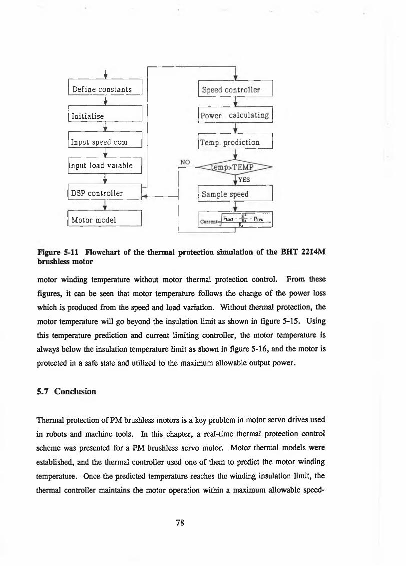
iDefine constantsIInit ialiseIInput speed com.I
Input load vaiableIDSP controller
Motor model Puai - + PpwuR.
Figure 5-11 Flowchart of the thermal protection simulation of the BHT 2214M brushless motor
motor winding temperature without motor thermal protection control. From these
figures, it can be seen that motor temperature follows the change of the power loss
which is produced from the speed and load variation. Without thermal protection, the
motor temperature will go beyond the insulation limit as shown in figure 5-15. Using
this temperature prediction and current limiting controller, the motor temperature is
always below the insulation temperature limit as shown in figure 5-16, and the motor is
protected in a safe state and utilized to the maximum allowable output power.
5.7 Conclusion
Thermal protection of PM brushless motors is a key problem in motor servo drives used
in robots and machine tools. In this chapter, a real-time thermal protection control
scheme was presented for a PM brushless servo motor. Motor thermal models were
established, and the thermal controller used one of them to predict the motor winding
temperature. Once the predicted temperature reaches the winding insulation limit, the
thermal controller maintains the motor operation within a maximum allowable speed-
78
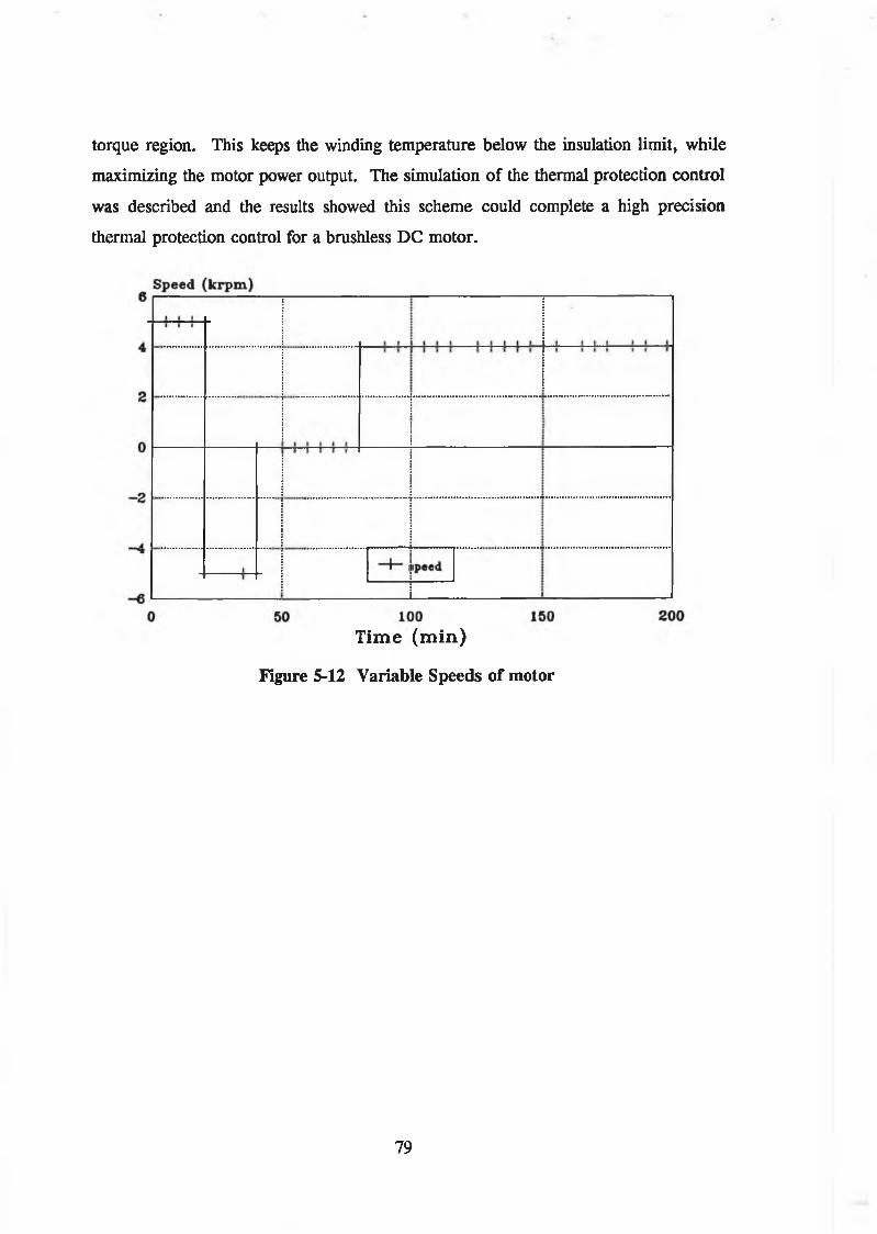
torque region. This keeps the winding temperature below the insulation limit, while
maximizing the motor power output. The simulation of the thermal protection control
was described and the results showed this scheme could complete a high precision
thermal protection control for a brushless DC motor.
Time (m in)
Figure 5-12 Variable Speeds of motor
79
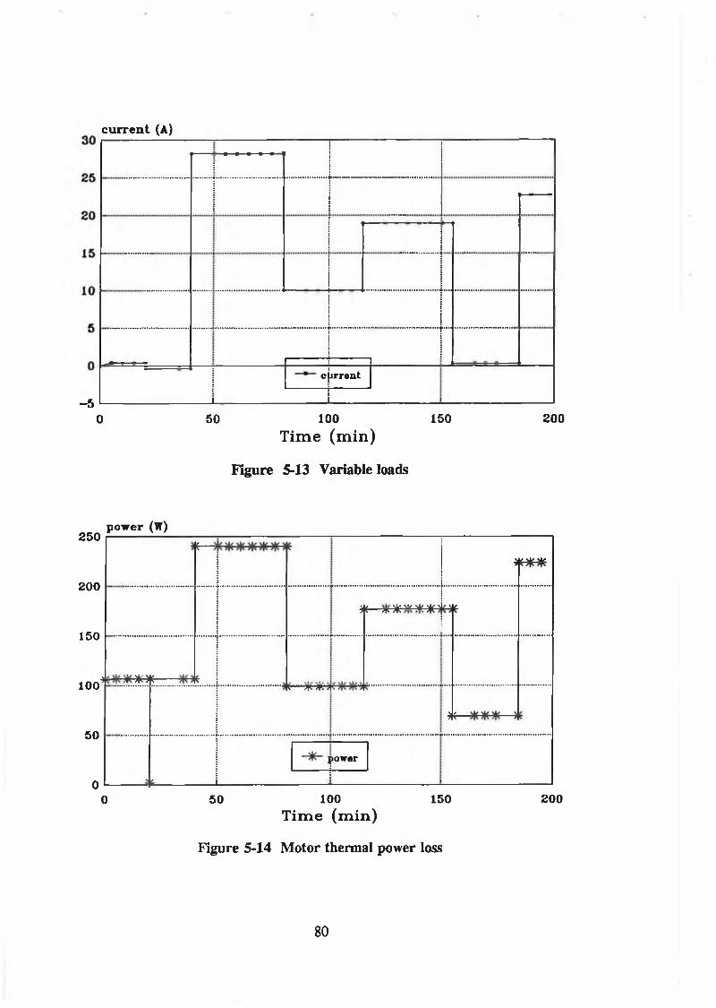
-50 50 100 150 200
T im e (m in )
Figure 5-13 Variable loads
power (W)250
200
150
100
50
0
0 50 100 150 200T im e (m in )
Figure 5-14 Motor thermal power loss
i----jI *
/ si/ \1/
j y], yt, \4” '4' ' |£i % nT* m m
: i *r>K------- *
s
*— xrxr*
...................hÉ ^
(■
s1
i
1lower
c u r r e n t (A)
-----i
1! 1 !
M
:
:i1:L .
c ir re n t
80
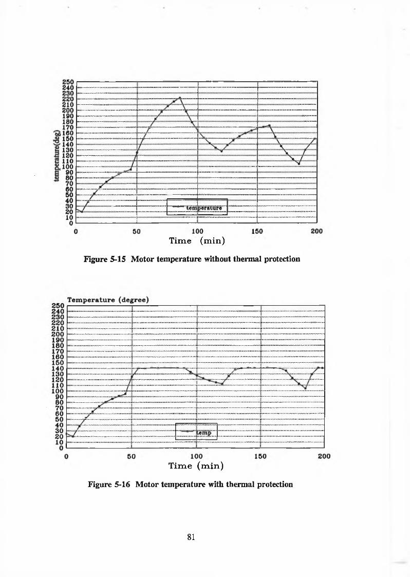
Time (m in)
Figure 5-15 Motor temperature without thermal protection
T im e (m in )
Figure 5-16 Motor temperature with thermal protection
81
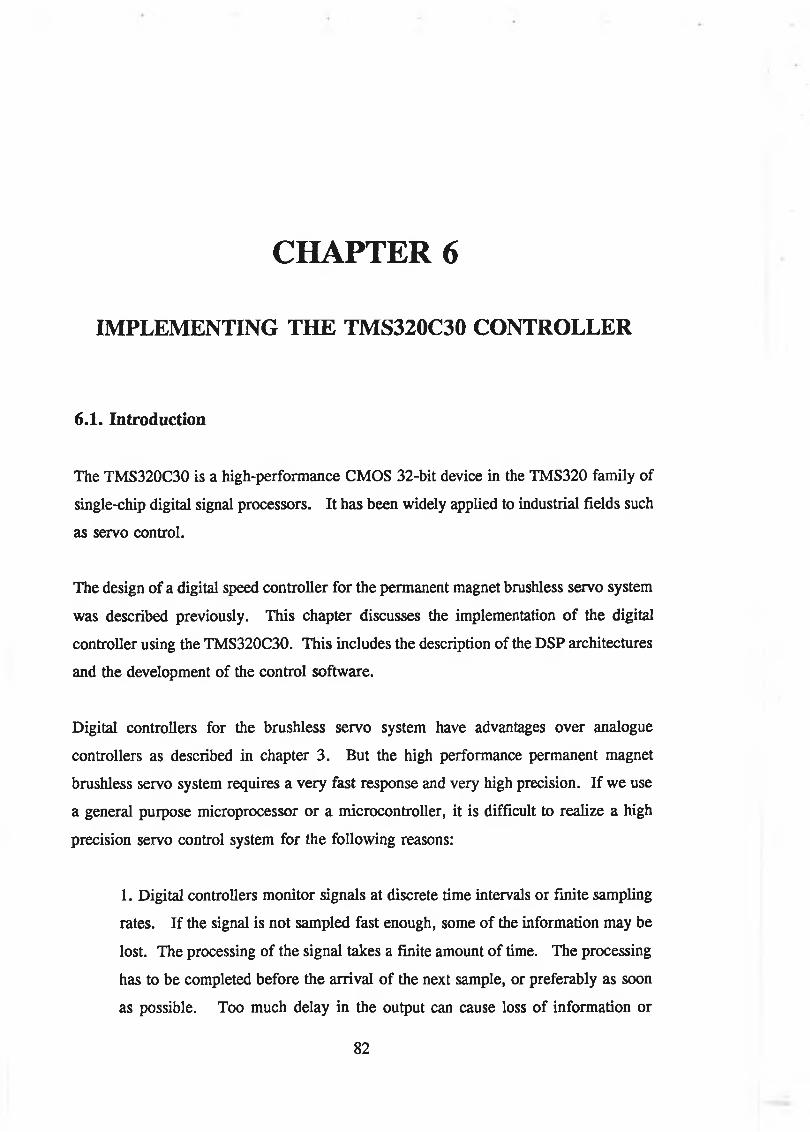
CHAPTER 6
IMPLEMENTING THE TMS320C30 CONTROLLER
6.1. Introduction
The TMS320C30 is a high-performance CMOS 32-bit device in the TMS320 family of
single-chip digital signal processors. It has been widely applied to industrial fields such
as servo control.
The design of a digital speed controller for the permanent magnet brushless servo system
was described previously. This chapter discusses the implementation of the digital
controller using the TMS320C30. This includes the description of the DSP architectures
and the development of the control software.
Digital controllers for the brushless servo system have advantages over analogue
controllers as described in chapter 3. But the high performance permanent magnet
brushless servo system requires a very fast response and very high precision. If we use
a general purpose microprocessor or a microcontroller, it is difficult to realize a high
precision servo control system for the following reasons:
1. Digital controllers monitor signals at discrete time intervals or finite sampling
rates. If the signal is not sampled fast enough, some of the information may be
lost. The processing of the signal takes a finite amount of time. The processing
has to be completed before the arrival of the next sample, or preferably as soon
as possible. Too much delay in the output can cause loss of information or
82
excessive phase delay in the system, leading to instability. These conditions
impose certain minimum performance requirements on the processor. Most of
the processors currently used to implement controllers are usually not fast enough
to process signals in real time, they rely upon lookup tables with precomputed
results. [6-4]
2. Digital controllers use discrete steps to represent a signal, which is limited to
the wordlength of the processor. Coefficients or gain constants also have to be
represented in the limited wordlength. This discretization or loss of resolution
is referred to as quantization error. In addition, results of mathematical
operations have to fit in a limited wordlength and may lose part of the result due
to this limitation. This is referred as truncation errors. Both of these errors
cause oscillations or limit cycles and can lead to instability.
3. Another problem that occurs in digital controllers is overflow of registers.
Successive mathematical operations can cause registers to overflow. Registers
in most processors wrap around, causing the result of a calculation to go from
most positive to least negative, in turn causing the output to reverse directions.
Most of these problems described above occur in processors that have 8 /16-bit ALUs
and registers. This 8 /16-bit architecture limits the accuracy of intermediate and final
results and generates truncation/quantization errors. Lack of scaling shifters to maintain
the required significant bit can cause additional quantization/truncation errors. The
general processors also lack the performance to perform fast real time processing, so
they rely upon lookup tables, thus limiting precision to low-performance or
low-bandwidth systems. If used in higher-performance systems, they can cause
excessive loop delays, leading to instability.
The problems discussed above can be eliminated by the TMS320C30. This is because
the TMS320C30 not only has an optimized architecture that minimizes numerical
problems in signal processing, but also has the performance to meet the bandwidth
requirements of high performance systems. The TMS320C30 has a fast execution speed
83

which minimizes the computation delay time and also allows very fast sampling rates to
be implemented for high bandwidth systems. In the TMS320C30, the fast arithmetic
operations and high throughput to handle mathematically intensive algorithms in real
time are accomplished by using the following concepts: hardware architecture using both
the Harvard and the von Neumann types; extensive four-phase pipelining in parallel; a
dedicated hardware multiplier; special DSP instruction; and a fast instruction cycle.
The TMS320C30 controller is implemented by a TMS320C30 PC system board which
consists of a TMS320C30 processor, expansion memories, a two-channel 16-bit analog
interface , a PC interface, a parallel expansion and a serial expansion. It is an
integrated 33.3 million floating-point computations per second signal-processing system
and provides a high-speed communication between the board and PC.
In this chapter, section 6.2 gives a general description of the TMS320C30 board.
Section 6.3 introduces the software design for the speed controller which uses the
TMS320C30 assembly language. Section 6.4, introduces a PC control program, which
is used to set the control input command and adjust the motor control parameters on PC.
In addition, appendix C describes an interface circuit design between the TMS320C30
board and the electronic controller of the servo system.
6.2. The TMS320C30 PC SYSTEM Board Description
6.2.1 Processor
The TMS320C30 DSP is a very fast processor which executes 16.7 million instructions
per second for an instruction cycle time of 60 nanoseconds. It has a large memory space
with 16 million 32-bit words and floating point arithmetic capabilities (32-bit
integer/40-bit floating-point multiplier and ALU). [6-1]
The TMS320C30, the third-generation device in the TMS320C30 family, can perform
parallel multiply and ALU operations on integer or floating-point data in a single cycle.
The processor also possesses a general-purpose register file, program cache, dedicated
84

auxiliary register arithmetic units, internal dual-access memories, one DMA channel
supporting concurrent I/O, and a short machine-cycle time.
The TMS320C30 can enhance general-purpose application by using the large address
space, multiprocessor interface, internally and externally generated wait states, two
timers, two serial ports, and multiple interrupt structure.
The TMS320C30 can use high-level language through a register-based architecture, large
address space, powerful addressing modes, flexible instruction set, and supports floating
point arithmetic.
6.2.2 Memory Map
The total memory space of the TMS320C30 is 16M 32-bit words. Programs, data, and
I/O space are contained within this, allowing tables, coefficients, program code, or data
to be stored in either RAM or ROM. RAM block 0 and 1 are each IK x 32 bit. The
ROM block is 4K x 32 bits. Each RAM and ROM block is capable of supporting two
accesses in a single cycle. They are separate program buses, data buses.
6.2.2.1 Memory Maps
The TMS320C30 board uses microprocessor mode memory map as shown in figure 6-1
with both the TMS320C30 DSP memory maps and TMS320C30 PC SYSTEM BOARD
memory maps.
6.2.2.2 Peripheral Bus Map
The memory-mapped peripheral registers are located starting at address 808000h. The
peripheral bus memory map is shown in figure. 6-2. Each peripheral occupies a 16-
word region of the memory map.
6 .2.2.3 Reset/Interrupt/Trap Vector Map
The address for the reset, interrupt, and trap vectors are Oh through 3Fh, as shown in
figure. 6-3. The vectors stored in these locations are the addresses of the start of
85
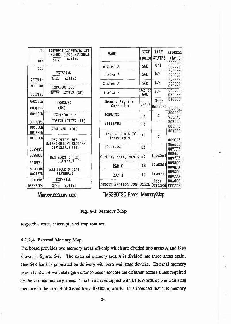
BANK SIZE
(VORDS)
WAIT
STATES
ADDRESS
(hex)
o Area A 64K 0/1OOO'OUUOOFFFF
1 Area A 64K 0/10100U001FFFF
2 Area A 64K 0/1 0 2 0 0 0 002FFFF
3 Area B16k or 64K
0/103000003FFFF
Memory Expsion Connector 7963K
User
Defined 7FFFFF
DSPLINK 8K 2800000901FFF
Reserved 8K802000803FFF
Analog I/O & PC Interrupts
8K 2
804000
805CFF
Reserved 8K806000807FFF
On-Chip Perigherals 6K Internal 8080008097FF
RAM 0 IK Interna] 809800809BFF
RAM 1 IK Internal 809CQO809FFF
Meiory Expsion Con, 8152KUserDefined
8OAOOOFFFFFF
OhBFh
INTERRPT LOCATIONS AND REVERED (192) EXTERNAL STRB ACTIVE
COhEXTERNAL
7FFFFFh STRB ACTIVE800000h EXPASION BUS801FFFh MSTRB ACTIVE (8K)802000h RESERVED803FFFh (8K)804000h EXPASION BUS805FFFh IOSTRB ACTIVE (81)806000h807FFFh RESERVED (81)soaoooh
8097F7hPERIPHERAL BUS MAPPED-MEM0RY REGISERS (INTERNAL) (6K)
8Q9800h809BFFh
RAM BLOCK 0 (IK) (INTRNAL)8D9C00h809FFFh
BAK BLOCK O (IK) (INTRNAL)BOAOOOh EXTERNAL
OFFFFfFh STRB ACTIVEMicroprocessor mode TMS320C30 Board Memory Map
Fig. 6-1 Memory Map
respective reset, interrupt, and trap routines.
6.2.2.4 External Memory Map
The board provides two memory areas off-chip which are divided into areas A and B as
shown in figure. 6-1. The external memory area A is divided into three areas again.
One 64K bank is populated on delivery with zero wait state devices. External memory
uses a hardware wait state generator to accommodate the different access times required
by the various memory areas. The board is equipped with 64 KWords of one wait state
memory in the area B at the address 30000h upwards. It is intended that this memory
86
808000h80800Fh
DMA CONTROLLER REGISTERS (16)
808010h 8 0 8 OlFh RESERVED (16)808020b80802Fh
TIMER 0 REGISERS (16)
808030h80803Fh
TIMER 1 REGISERS (16)
808040h80804Fh
SERIAL PORT 0 REGISERS (16)
808050h80805Fh
SERIAL PORT 1 REGISERS (16)
808060h80806Fh
PRIMARY AND EXPASION PORT REGISERS (16)
I8§8?PÈ RESERVED (16)
Figure 6-2 Peripheral bus memory map
OOh RESETO lh INTO02h INTI0 3h INT20 4h INT30 5h XINTO0 6h RINTO0 7h XINT108h RINT10 9h TINTOOAh TINT1OBh DINT
OCh RESERVED ..2 Oh TRAPO...3Ch TRAP 28 (RESERVED)...3Fh TRAP 31 (RESERVED)
Figure 6-3 Reset, Interrupt, and Trap vector locations
be used for the transfer of the data between PC and the TMS320C30.
87
6.2.3 Analog interface
It is necessary for the TMS320C30 based servo control system to use A/D and D/A
conversion. The TMS320C30 PC SYSTEM BOARD contains a complete "analog I/O
subsystem". There are two separate channels, each containing its own sample/hold
amplifier, A/D, D/A, and analog filters on input and output. The analog I/O signals are
accessed via the "end-plate", which is accessible through the back of the PC. The A/D’s
are Burr-Brown PCM78P devices which offer 16-bit precision with up to 200 kHz
sample rates. The sample/hold amplifiers and D/A converters are also Burr-Brown
devices which are matched to the capabilities of the A/D. The sample/hold device is the
SHC5320, and the D/A device is the PCM56P. The conversion is triggered by timer
1 (the 32-bit on-chip timer) which can be programmed by software to a resolution of
120nsec. The analog I/O subsystem is accessed through three 16-bit secondary I/O bus
mapped registers. They are in the region between the address 804000 hex and 804008h
as shown in Table 1.
Table 1 Analog I/O Mapping
Address Function
804000h Read/Write Channel A’s A/D & D/A
804001h Read/Write Channel B’s A/D & D/A
804008h Software Conversion Trigger
Although each register consumes 32 bits of space, only the top 16 bits of each register
are used. The first two registers are used to access the A/D and D/A converters on the
two Analog I/O channels. The A/D’s and D/A’s deal with data in 16-bit 2 ’s
complement format. All the registers are accessed with two memory wait states. This
results in an overall time of 180 nsec to access each register.
88
6.3. Software design for TMS320C30 board
6.3.1 Selection of Software tools
The TMS320C30 is well supported by a full set of software development tools which
include assembly-language, C language or a mixed combination. In brushless motor
control, the real time control program must execute as fast as possible. In our
application, the program is written in assembly-language. Although C is easier to use
than assembly, it is slower in the control mode. For example, most of DSP algorithms
spend the vast majority of execution time on a small section of code (Normally 90
percent of the time is spent on 1 0 percent of the code.) [6 -8 ],
6.3.2 Program flowchart
The program flowcharts are shown in figure 6-4. The TMS320C30 assembly language
uses a number of ‘sections’, which are relocatable blocks of code or data, to execute a
program. In the program, interrupt vectors are located in the section ". in i t" beginning
at address Oh. The ".d a ta " section contains register addresses, control words and initial
variables. The ".text" section executes the program which is divided into two main parts
the initial routine and control routine as described below.
6.3.2.1 Initializing routine
This routine consists of a page pointer, stack pointer, external bus operation, timer, and
wait states.
(1) Data Page PointerIn order to use direct addressing, the page pointer is set up first. In the direct
addressing mode, the data address is formed by the combination of the 8 least significant
bits of the data page pointer (DP) with the 16 least significant bits of the instruction
word (expr). This produces 256 pages of space, and gives the programmer enough
memory space without needing to change the page pointer. The syntax of the page
pointer is LDP which is expressed as :
89
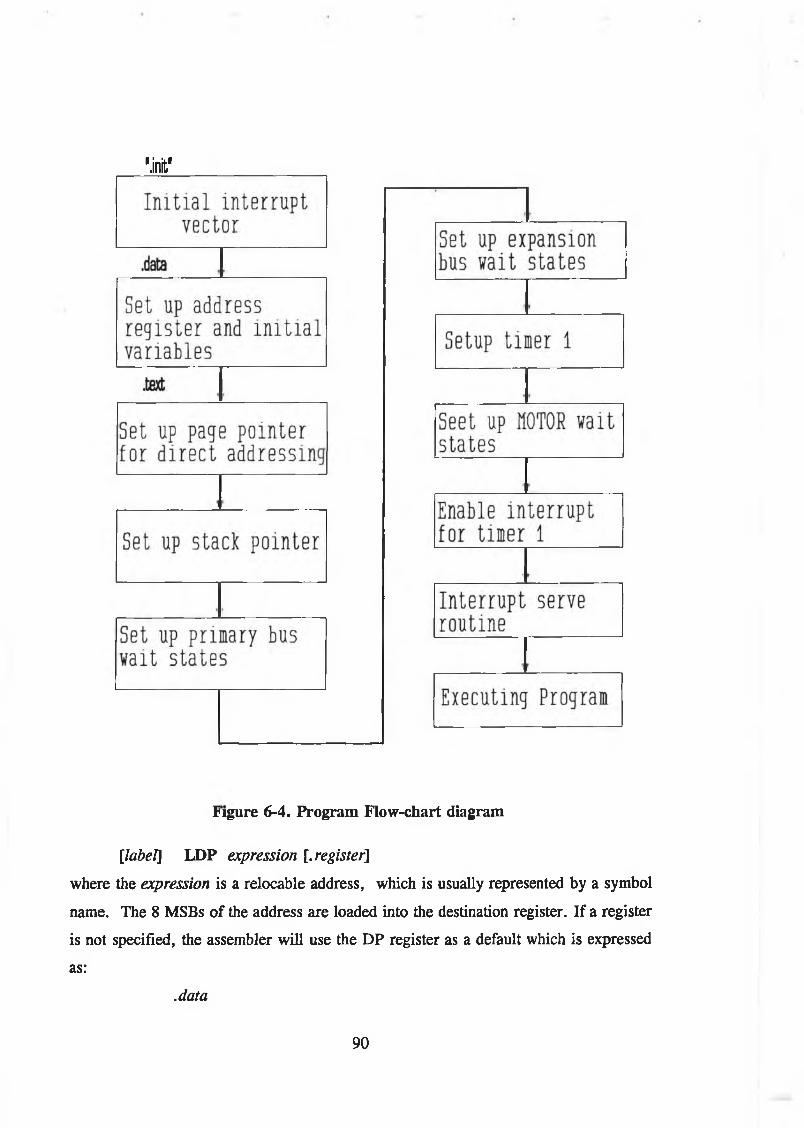
'.¡nit'
Figure 6-4. Program Flow-chart diagram
[ la b e l] LDP e xp re ss io n [.re g is te r ]
where the e xp re ss io n is a relocable address, which is usually represented by a symbol
name. The 8 MSBs of the address are loaded into the destination register. If a register
is not specified, the assembler will use the DP register as a default which is expressed
as:
.d a ta
90
P R 1M C T L .w o rd 0 0 8 0 8 0 6 5 k
.te x t
L P D P R IM C T L
The P R IM C T L as an address variable located at the ".data" section, the LDP instruction
loads the DP register with the 8 -bit pointer to the page on which P R IM C T L is located.
Note that the re g is te r operand was omitted from the L D P instruction; D P was used as
the default.
(2) Stack pointerThe TMS320C30 provides a dedicated system stack pointer (SP) for building stacks in
memory. The program counter is pushed on the system stack on interrupt. It is popped
from the system stack on return. The syntax of the stack pointer is expressed as:
.d a ta
R S P .w o rd S T A C K
S T A C K .w o rd 0
.te x t
L D I @ R S P ,S P
where S P is the stack pointer.
(3) External Bus OperationTwo external interfaces are provided on the TMS320C30: the primary bus and the
expansion bus. The TMS320C30 processor uses them to access data between memory
and external peripheral devices. The primary bus consists of a 32-bit data bus and a 24-
bit address bus. The expansion bus consists of a 32-bit data bus and a 13-bit address
bus. Both the primary bus and the expansion bus have associated control registers which
are memory-mapped in table 2 .
Table 2. Memory-mapped External Interface Control Register
Peripheral Address Register
808060h Expansion bus control
808064h Primary bus control
91
For the TMS320C30 SYSTEM BOARD operation, the external memory area A must
always be configured via the primary bus control register to respond only to externally-
controlled wait states. That allows external hold requests and can have a 64KWord bank
size. Bits 8-12 of the primary bus control register called BNKCMP determine the size
of the bank as shown in table 3.
Table 3. BNKCMP and Bank Size
BNKCMP MSBs DEFINING A BANK BANK SIZE (32-BIT WORDS)
0 0 0 0 0 None 2M = 16M
0 0 0 0 1 23 2* = 8 M
0 0 0 1 0 23-22 2 n = 4M
0 0 0 1 1 23-21 221 = 2M
0 0 1 0 0 23-20 220 = 1M
0 0 1 0 1 23-19 219 = 512K
0 0 1 1 0 23-18 218 = 256K
0 0 1 1 1 23-17 217 = 128K
0 1 0 0 0 23-16 2 U = 64K
0 1 0 0 1 23-15 215 = 32K
0 1 0 1 0 23-14 214 = 16K
0 1 0 1 1 23-13
00IICN
0 1 1 0 0 23-12 212 = 4K
0 1 1 0 1 23-11 211 = 2K
0 1 1 1 0 23-10 210 = IK
0 1 1 1 1 23-9 29 = 512
1 0 0 0 0 23-8 28 = 256
1 0 0 0 1 Reserved Undefined
to
1 1 1 1 1
The bold number 01000 determines the bank size of the area A which is 64Kwords.
After a reset, the primary bus control register sets a control word 800h corresponding
to 01000. The expansion bus control register is set up by writing Oh. The program for
92
the external operation is:
EXPCTL
PR1MWD
PR1MCTL
.d a ta
.w o rd 0 0 8 0 8 0 6 4 h ; P r im a ry bus
.w o rd 0 0 8 0 8 0 6 0 h ; E xp a n s io n bus
.w o rd 0 0 0 0 0 8 0 0 h ; P rim a ry bus c o n tro l w o rd
E X P W D . w o rd 0 0 0 0 0 0 0 0 h ; E xp a n s io n b us c o n tro l w o rd
.text
; S e t u p p r im a ry bus w a it s ta tes
L D I © P R IM C Il, ARO
L D I © P R IM W D , R O
S T 1 R 0 , *A R O
; S e t up e xp a n s io n bus w a it s ta te s
L D I @ E X P C T L , ARO
L D I © E X P W D , RO
S T IR O , *A R 0
(4) Timer set up
The TMS320C30 provides two internal timers, timer 0 and timer 1. The TMS320C30
system board uses the timer 1 to signal the external A/D converter to start a conversion
with an internal clock. The timer modules are general-purpose 32-bit timer/event
counters with two signalling modes and internal or external clocking as shown in figure
6-5. Three memory-mapped registers are used by the timer which are the global control
register, period register and counter register. The timer global control register is a 32-
bit register that contains the global and port control bits for the timer module in which
the bits 3 to 0 are the port control bits and the bits 11 to 6 are the timer global control
bits. The global control register determines the timer operating mode, monitors the
timer status, and controls the function of the I/O pin of the timer. The 32-bit timer
period register specifies the timer’s signalling frequency. The counter register is also
a 32-bit register which contains the current value of the increment counter. The counter
is zeroed whenever its value equals that in the period register. The memory map of
93
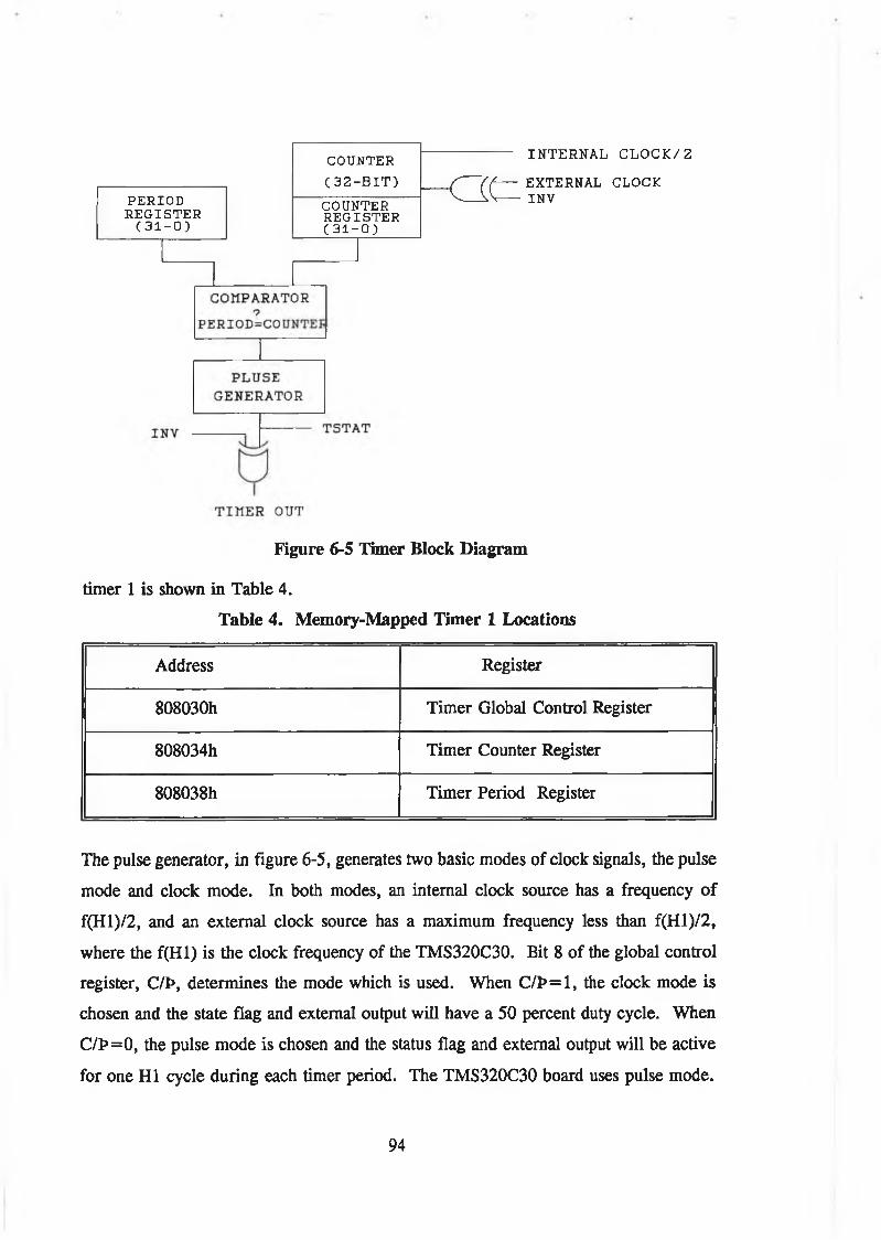
PERIODREGISTER( 3 1 - 0 )
COUNTER(32-BIT)COUNTERREGISTER(31-0)
-atINTERNAL C L O C K / 2EXTERNAL CLOCK INV
Figure 6-5 Timer Block Diagram
timer 1 is shown in Table 4.
Table 4. Memory-Mapped Timer 1 Locations
Address Register
808030h Timer Global Control Register
808034h Timer Counter Register
808038h Timer Period Register
The pulse generator, in figure 6-5, generates two basic modes of clock signals, the pulse
mode and clock mode. In both modes, an internal clock source has a frequency of
f(Hl)/2, and an external clock source has a maximum frequency less than f(Hl)/2,
where the f(Hl) is the clock frequency of the TMS320C30. Bit 8 of the global control
register, C/I>, determines the mode which is used. When C/1>=1, the clock mode is
chosen and the state flag and external output will have a 50 percent duty cycle. When
C/I>=0, the pulse mode is chosen and the status flag and external output will be active
for one HI cycle during each timer period. The TMS320C30 board uses pulse mode.
94
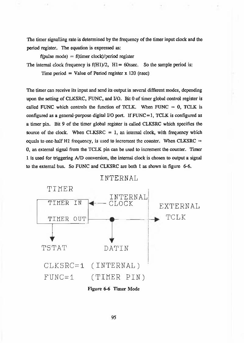
The timer signalling rate is determined by the frequency of the timer input clock and the
period register. The equation is expressed as:
f(pulse mode) = f(timer clock)/period register
The internal clock frequency is f(Hl)/2, HI = 60nsec. So the sample period is:
Time period = Value of Period register x 120 (nsec)
The timer can receive its input and send its output in several different modes, depending
upon the setting of CLKSRC, FUNC, and I/O. Bit 0 of timer global control register is
called FUNC which controls the function of TCLK. When FUNC = 0, TCLK is
configured as a general-purpose digital I/O port. If FUNC = 1, TCLK is configured as
a timer pin. Bit 9 of the timer global register is called CLKSRC which specifies the
source of the clock. When CLKSRC = 1, an internal clock, with frequency which
equals to one-half HI frequency, is used to increment the counter. When CLKSRC =
0, an external signal from the TCLK pin can be used to increment the counter. Timer
1 is used for triggering A/D conversion, the internal clock is chosen to output a signal
to the external bus. So FUNC and CLKSRC are both 1 as shown in figure 6 -6 .
T I M E RTIMER IN
TIMER OUT
INTERNAL
INTERNAL CLOCK
tTSTAT
tDATIN
EXTERNAL > TCLK
C L K S R C = 1 (I N T E R N A L ) FUNGHI (TIMER PIN)
Figure 6 - 6 Timer Mode
95

Bit 10 of the global control register is the inverter control bit and is called INV. If
INV= 1, the output o f the pulse generator is routed to TCLK. If INV=0, no inversion
is performed on the output or input of the timer. Bits 7 and 8 of the global control
register control the timer reset, start and hold as shown in table 5.
Table 5. Result of a Write of Specified Values of GO and HLD
GO HLD RESULT
0 0 All timer operations are held. No reset is performed.
0 1 Timer proceeds from state before write.
1 0 All timer operations are held, including zeroing of the counter.
The GO bit is not cleared until the timer is taken out of hold.
1 1 Timer reset and started.
The timer global control register is shown in figure 6-7.
31 30 29 26 27 26 25 24 23 22 21 20 19 18 17 16
n XX XX XX X X XX XX XX XX XX XX XX XX XX XX XX
15 1 4 1 3 12 11 10 9 8 7 6 5 4 3 2 1 0XX XX XX XX TSTAT INV CLKSRC C/P HLD GO XX XX DATIN DAT0UT i / o FUNC
R/V R/V R/V R/V R/V R/V R R/V R/V R/V
Note: xx = Reserved bit, read as o. R = read, 'i - write.
Figure 6-7 Timer Global Register
96
When resetting the timer, 601h is loaded into the global control register, where the
respective bits 0, 9, and 10 are set to 1. While starting the timer, 6 Clh is used and the
respective bits 0, 6 , 7, 9 and 10 are set to 1. The program for setting timer 1 is:
T IM E C T L
.d a ta
.w o rd 0 0 8 0 8 0 3 0 k ; T im e r 1 c o n tro l re g is te r
P E R IO D .w o rd 0 0 8 0 8 0 3 8 k ; T im e r 1 p e r io d re g is te r
R S T C IR L .w o rd 0 0 0 0 0 6 0 1 k ; R ese t c o n tro l w o rd
S E T C T R L .w o rd 0 0 0 0 0 6 C lk ; S ta r t tim e r c o n tro l w o rd
S A M P L E .w o rd 2 0 0 0 ; S am p le p e r io d
.te x t
;S e t up tim e r 1.
L D I @ T IM E C T R L , A R O
L D I @ R S T C T R L, RO
S T IR O , *A R 0
L D I @ P E R IO D , RO
L D I @ S A M P LE , RO
S T IR O , *A R 1
L D I @ S E T C T R L, RO
S T IR O , *A R 0
; R eset c o n tro l re g is te r
; S et p e r io d re g is te r
; S ta rt tim e r 1
(5) Interrupt control
The TMS320C30 can execute an interrupt control in different ways as shown in figure
6- 8 .
The TMS320C30 system board uses the CPU external hardware interrupt. The logic
function diagram used to implement the interrupt is shown in figure 6-9.
After the timer starts an A/D conversion, the A/D performs the conversion, then
outputs an end-of-convert signal which triggers the INTL interrupt request.
97
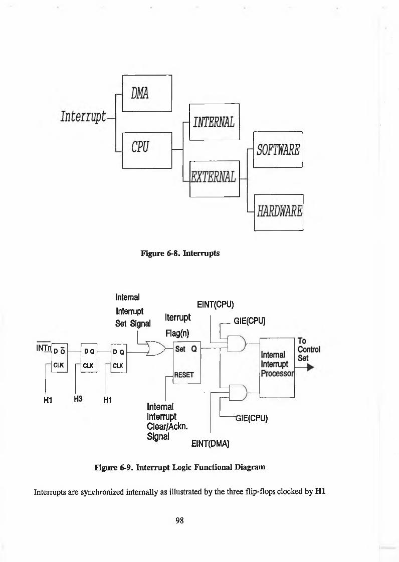
figure 6 -8 . Interrupts
INTn D Q
CLK
H1
d q
CLX
D Q
CLK
IterruptInternal
InterruptSet Signal
Flag(n)
i>H
EINT(CPU) GIE(CPU)
H1InternalinterruptClear/Ackn.Signal
GIE(CPU)
EINT(DMA)
Figure 6-9. Interrupt Logic Functional Diagram
Interrupts are synchronized internally as illustrated by the three flip-flops clocked by HI
98
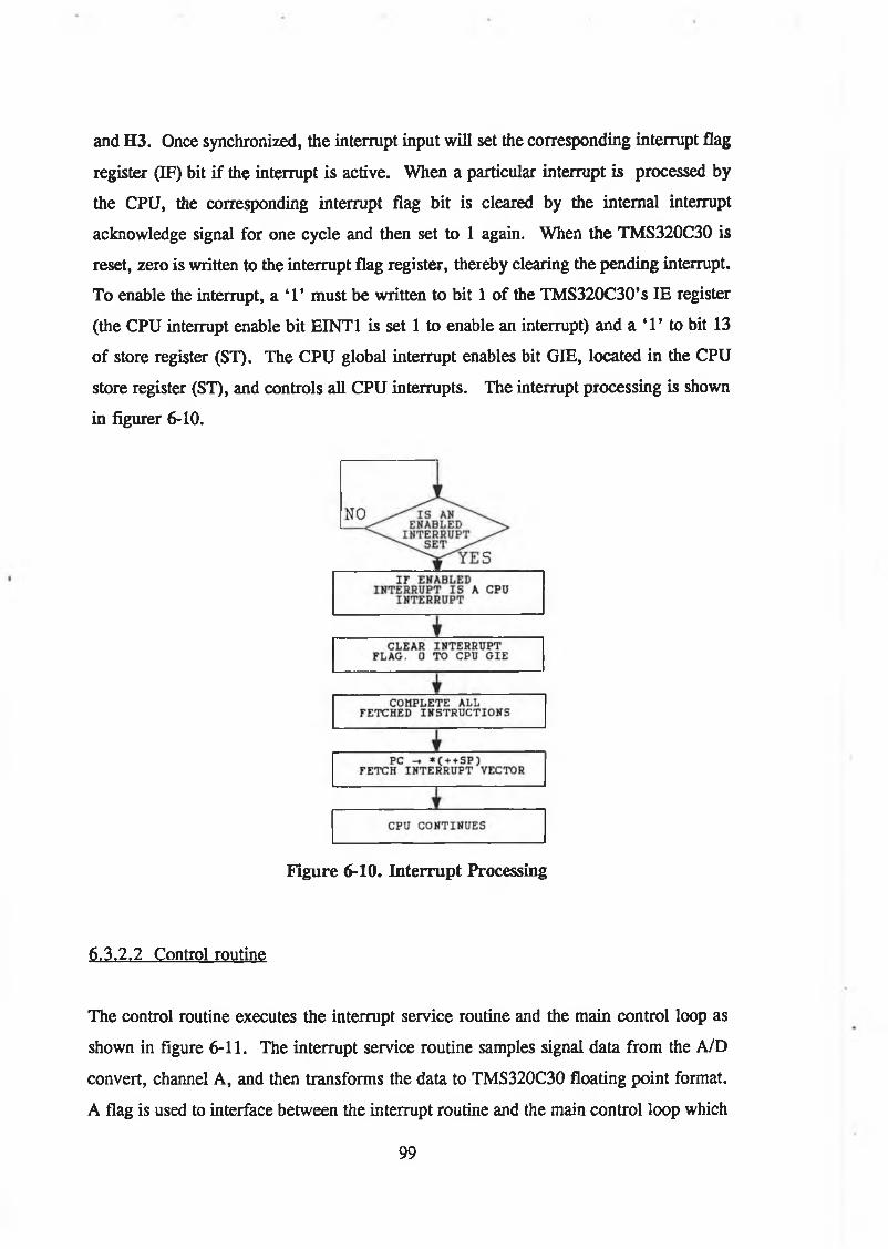
and H3. Once synchronized, the interrupt input will set the corresponding interrupt flag
register (IF) bit if the interrupt is active. When a particular interrupt is processed by
the CPU, the corresponding interrupt flag bit is cleared by the internal interrupt
acknowledge signal for one cycle and then set to 1 again. When the TMS320C30 is
reset, zero is written to the interrupt flag register, thereby clearing the pending interrupt.
To enable the interrupt, a ‘1’ must be written to bit 1 of the TMS320C30’s IE register
(the CPU interrupt enable bit EINT1 is set 1 to enable an interrupt) and a ‘1’ to bit 13
of store register (ST). The CPU global interrupt enables bit GIE, located in the CPU
store register (ST), and controls all CPU interrupts. The interrupt processing is shown
in figurer 6 - 1 0 .
Figure 6-10. Interrupt Processing
6.3.2,2 Control routine
The control routine executes the interrupt service routine and the main control loop as
shown in figure 6-11. The interrupt service routine samples signal data from the A/D
convert, channel A, and then transforms the data to TMS320C30 floating point format.
A flag is used to interface between the interrupt routine and the main control loop which
99
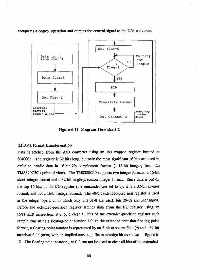
completes a control operation and outputs the control signal to the D/A converter.
Figure 6-11 Program Flow chart 2
(1) Data format transformationData is fetched from the A/D converter using an I/O mapped register located at
804000h. The register is 32 bits long, but only the most significant 16 bits are used in
order to handle data in 16-bit 2 ’s complement format (a 16-bit integer, from the
TMS320C30’s point of view). The TMS320C30 supports two integer formats: a 16-bit
short integer format and a 32-bit single-precision integer format. Since data is put on
the top 16 bits of the I/O register (the remainder are set to 0), it is a 32-bit integer
format, and not a 16-bit integer format. The 40-bit extended-precisión register is used
as the integer operand, in which only bits 31-0 are used, bits 39-32 are unchanged.
Before the extended-precisión register fetches data from the I/O register using an
INTEGER instruction, it should clear all bits of the extended-precisión register each
sample time using a floating-point number 1.0. In the extended-precisión floating-point
format, a floating-point number is represented by an 8 -bit exponent field (e) and a 32-bit
mantissa field (m a n ) with an implied most-significant nonsign bit as shown in figure 6 -
12. The floating point number, = 0.0 can not be used to clear all bits of the extended-
100
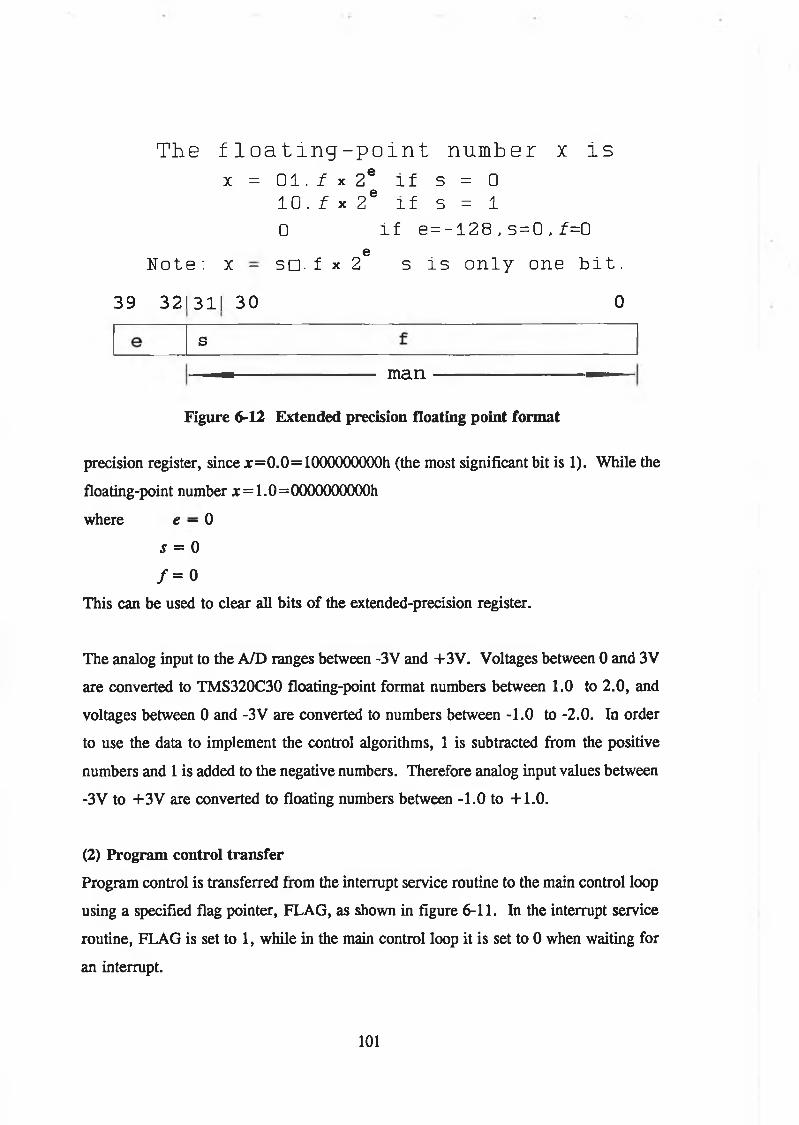
The floating-point number x isx = 0 1 .f x 2® if s = 0
10. f X 2e if s = 1 0 if e=-128,s = 0 ,f=0
eNote: x - sm. f x 2 s is only one bi t .
39 32131] 30 0s
manFigure 6-12 Extended precision floating point format
precision register, since * = 0 .0 = 1000000000h (the most significant bit is 1). While the
floating-point number x = 1 . 0 = 0 0 0 0 0 0 0 0 0 0 h
where e — 0
s = 0
/ = 0
This can be used to clear all bits of the extended-precisión register.
The analog input to the A/D ranges between -3V and +3V. Voltages between 0 and 3V
are converted to TMS320C30 floating-point format numbers between 1.0 to 2.0, and
voltages between 0 and -3V are converted to numbers between -1.0 to -2.0. In order
to use the data to implement the control algorithms, 1 is subtracted from the positive
numbers and 1 is added to the negative numbers. Therefore analog input values between
-3V to +3V are converted to floating numbers between - 1 . 0 to + 1 .0 .
(2) Program control transferProgram control is transferred from the interrupt service routine to the main control loop
using a specified flag pointer, FLAG, as shown in figure 6-11. In the interrupt service
routine, FLAG is set to 1, while in the main control loop it is set to 0 when waiting for
an interrupt.
101
(3) Motor control routineIn this routine, for design I, the motor control algorithm uses:
u ( n ) = u ( n - l ) + 9 . 3 9 [ e ( / i ) - 0 . 9 9 3 3 5 e ( / i - l ) ]
which is described in section 3.4.3.
For the design n , the control program can be written as
e(kT0 = r(kT) - c(kT)
u,(kT) = KjeCkT) + ^[(k-iyT]
u(kT) = -KpC(kT) - KD{c(kT) - c[(k-l)T]} + Ul(kT)
which is detailed in section 3.5.
(4) Data outputData outputting to the D/A is the opposite to data inputting from the A/D. However,
the output data must be -2 .0 < x < 2 .0 , otherwise, we have to let x = -1.99999999 when
jc<-2.0, and x = 1.99999999 when x > 2 . 0 . Note that the floating-point number x can
not be - 2 . 0 or 2 . 0 which is zero when being converted to the integer format form.
6.4. PC control program
A PC control program is used to control the TMS320C30 board. It downloads the DSP
program to the TMS320 board, sets coefficients for the DSP program and sets the input
commands. The PC program allows the user to modify parameters of the controller.
The flowchart of the program is shown in figure 6-13. The program, which is written
in C, is presented in appendix B.
6.5 Conclusion
This chapter has discussed implementation of the digital controller for the brushless
servo system using the TMS320C30 processor. This system has numerous advantages
over analogue-based designs because its high processing speed allows sophisticated
digital control techniques to be used to build a high-precision servo control system. The
102
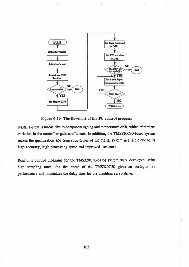
Figure 6-13 The flowchart of the PC control program
digital system is insensitive to component ageing and temperature drift, which minimizes
variation in the controller gain coefficients. In addition, the TMS320C30-based system
makes the quantization and truncation errors of the digital system negligible due to its
high accuracy, high processing speed and improved structure.
Real time control programs for the TMS320C30-based system were developed. With
high sampling rates, the fast speed of the TMS320C30 gives an analogue-like
performance and minimizes the delay time for the brushless servo drive.
103
CHAPTER 7PERFORMANCE MEASUREMENT
7.1 Introduction
In the previous chapters, we described the design of the digital controller for the
brushless motor servo system and the implementation on the DSP-TMS320C30. The
testing of the designed brushless motor servo system is presented in this chapter. In
order to identify the design performance of the system, a series of measurements of the
speed responses need to be performed, the results show a high performance of the
variable speed control for the TMS320C30 based servo drive system.
7.2 Experimental Equipment and Procedure
The experimental setup consists of a BHT 2214M brushless motor, a BHT controller,
a BHT power supply, a TMS320C30 PC system board, an IBM PC and a HP digital
oscilloscope as shown in figure 7-1. The servo drive system includes the motor, the
controller, the power supply and the TMS320 board. A PC is used to operate this
system. The dynamic characteristics of this system are measured by the oscilloscope and
the waveforms are sent to PC. The whole procedure is described as follows.
The three phase AC 380 volt power source is fed into a transformer which reduces the
voltage to three phase 220V. The BHT power supply rectifies the AC 220V voltage to
DC 300 V which is required by the inverter in the BHT controller. An interface circuit
is built to converts + /- 10V signal voltage to + /- 3V for the TMS320C30 system board.
The signal from the tachogenerator is fed into the A/D converter of the TMS320C30
board. The signal of the D/A converter is fed to the current loop of the BHT controller
104

to control the servomotor.
The speed performances are measured at the test point of the tachogenerator on the BHT
controller board using the HP digital oscilloscope. The waveforms of the oscilloscope
are drawn using a drawing package HG.
7.3 Tests of the servo system
7.3.1 Design I Test
The design I system is tested to investigate the design quality. A speed step response
from 3000 rpm to 0 is presented to the design I system which can demostrate the
overshoot. Figure 7-2 (a) shows the measured result, the overshoot is 10.3% and the
settling time is about 0.07 sec. Figure 7-2 (b) is the simulated step response,
respectively. The overshoot is about 10% and settling time is 0.064 sec. Both results
show the design meets the requirement in the section 3.4.2 where the desired overshoot
is 8 .1 % and the settling time is 0.062 sec. This proves the design is successful since
it eliminates steady-state error and has a fast dynamic response.
7.3.2 Design II Test
The design II system is tested to inspect the system dynamic response. The speed step
response from 3000 rpm to 0 is presented. Figure 7-3 (a) shows the measure result of
the speed dynamic response, the overshoot is 2 2 % and the settling time is about 0.028
sec. Figure 7-3 (b) is the simulated step response, respectively, in which the overshoot
is about 20% and the settling time is 0.025 sec. The requirements of the design II
system is an overshoot of 20% and a settling time of 0.02 sec. Both results show the
design meets the requirements since it has a faster dynamic response than the design I,
also it eliminated the steady-state error and it is controlled within the stability margin.
105
7.3 Sensitivity to controller parameters
For digital PID implement, the system performance is sensitive to changes in the
controller parameters KP, Kx and the DSP sampling rate. Design II system is used to
observe the effects. First, we investigated the effect of varying the parameter Kp as show
in figure 7-4. KP was varied from 25 to 20, 18 and 15 with the rest parameters
constant: K^O.25, KD=50 and the sample rate=0.12 msec. The figures show that with
larger the value of KP, the overshoot of the responses becomes smaller, hence KP has
significant affect on the system. Second, we investigated the influence of K j on the
system as shown in figure 7-5. Kj was adjusted from 0.15 to 0.3, where the rest of
parameters were constant: KP=15, KD=50 and sample rate = 0.12 msec. The figures
show that with larger KI? the overshoot of the responses becomes higher, so Kt also has
a significant affect on the system. Then, we investigated the influence of the sample rate
on the system as show in figure 7-6. The sample rates were varied from 0.06 msec to
1 msec with the rest of the parameters were constant: KP=15, Ki=0.25 and KD=50.
The figures show that with faster the sample rate, the overshoot of the responses
becomes higher, therefore the sample rate affects the system significantly as well.
This sensitivity is a disadvantage of the feedback and forward PID control, but if we use
grapho-analytical method of pole-placement, suitable parameters can be selected for a
desired performance of the system. Therefore we need not to do much trial and error
work to adjust the system.
7.4 Conclusion
The simulation and experimental results show the designed DSP based brushless drive
system is able to implement a high performance servo operation. Both designs can
eliminate steady-state error, have a fast dynamical response and have stability in the
steady-state. However, design n has a much faster dynamical response than design I,
this is very important for the high-performance servo applications. Although the PID
control is sensitive to the parameters of the controller, we can obtain a desirable
performance using the graph-analytical method of pole-placement.
106
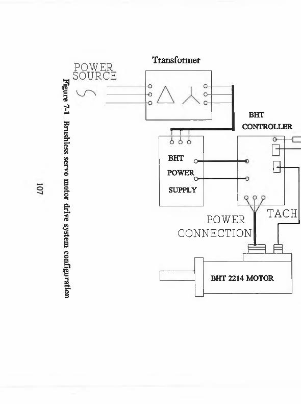
Figure 7-1
Brushless servo
motor drive
system configuration
POWERSOURCETransformer
BHT o.
POWERoSUPPLY
BHTCONTROLLER
0 -&
POWERCONNECTION
TACH
BHT 2214 MOTOR
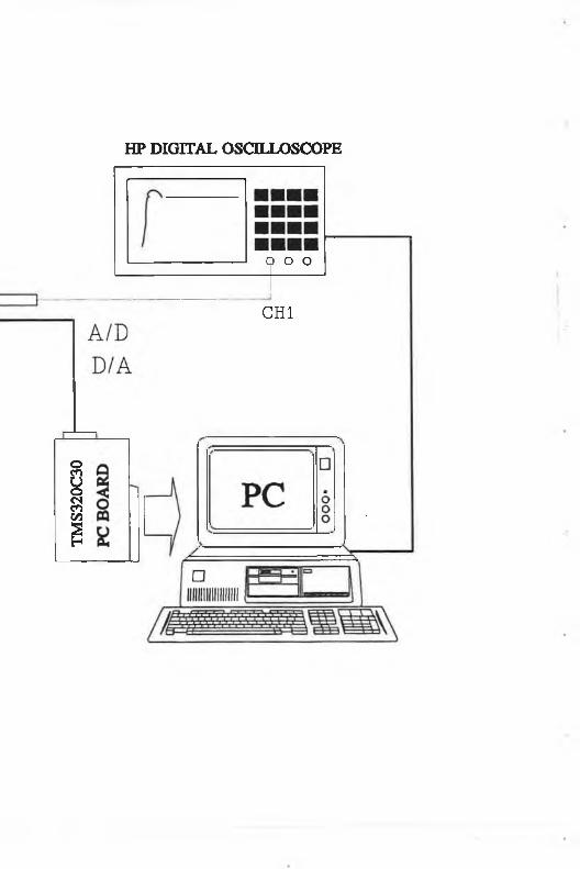
TMS3
20C
30
HP DIGITAL OSCILLOSCOPE
O O O
CHI
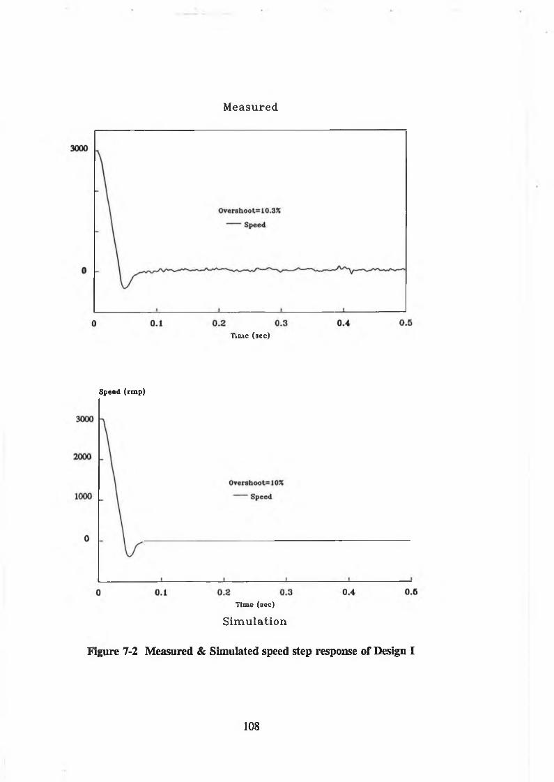
M easured
Time (sec)
Speed (rmp)
T im e ( s e c )
Sim ulation
Figure 7-2 Measured & Simulated speed step response of Design I
108
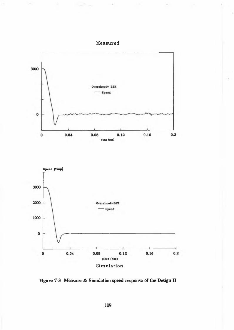
M easured
Time (wo)
Speed (im p )
T im e ( s e c )
Sim ulation
Figure 7-3 Measure & Simulation speed response of the Design II
109
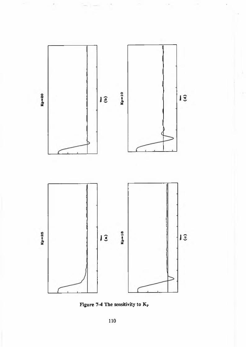
Figure 7-4 The sensitivity to KP
110
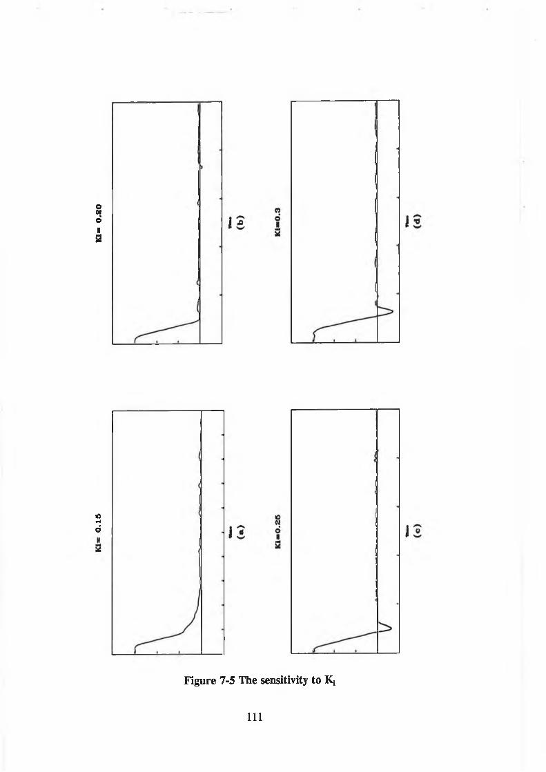
0.15
Kl
- 0
.20
Figure 7-5 The sensitivity to Kj
111
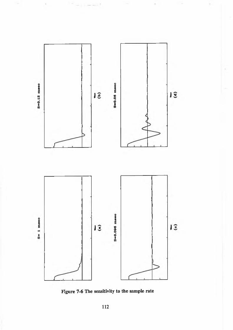
Figure 7-6 The sensitivity to the sample rate
112
CHAPTER 8CONCLUSIONS AND RECOMMENDATIONS
8.1 Conclusions
This thesis outlines a design methodology for digital speed servosystems and their
thermal protection control using a Texas Instruments TMS320C30 microprocessor. The
design methodology applied throughout this thesis is based on following phases:
• System description
• Plant modelling
• Controller design and analysis
• System simulation
• Brushless motor thermal protection control
• TMS320C30 implementation
• Experimental test
A permanent magnet brushless DC servo system was generally described in Chapter 2,
it is consist of a brushless motor, an electronic commutator and control system and a
sensing system. The control type is a current-controlled brushless DC motor servo
system with a PWM operation. The servo system model is based on a commercial PM
brushless drive.
The research focused on the digital speed controller design for a brushless drive. Two
methods were used, an "analogue design method for a digital controller" and a "grapho-
analytical method of pole-placement". The first one used well-known analogue design
technology to design an analogue speed controller which is then transformed to a digital
113
form. For the existing analogue system, using this scheme, the design becomes very
simple and easy. The second one used a digital forward and feedback PID controller,
in which parameters were adjusted using a graph-analytical method of pole-placement.
This controller has a faster response and greater accuracy than the first traditional PI
implementation but is more complex. This scheme eliminated the steady-state error of
the system and the controller parameters were adjusted for the desired accuracy,
response speed and stability margin of the system.
A simulation scheme, written in C, was developed for the designed digital servo system.
For the simulation scheme, the dynamic performance of the system can be investigated
and examined simply using the flowchart of the system transfer functions. By comparing
the results of the simulation and the experimentation, we can see the scheme accurately
demonstrated the performance of the system.
Thermal protection of PM brushless motors is a key problem in motor servo drives used
in robots and machine tools. In this thesis, a real-time thermal protection control
scheme was presented for the PM brushless servo motor. A thermal model of the motor
was established, and the thermal controller used this to predict the temperature of the
motor windings. Once the predicted temperature reaches the winding insulation limit,
the thermal controller limits the motor current to maintain operation within a maximum
allowable speed-torque region. This keeps the winding temperature below the insulation
limit, while maximizing the motor power output. The simulation results showed a
precise thermal protection control.
The digital speed controller was implemented with a digital signal processor, the
TMS320C30. The control software program was developed to perform a fast and high
precision speed control for the brushless servo drive.
The TMS320C30 based adjustable speed system was tested on a AEG BHT 2214M
brushless servo motor. A series of measurement results showed a successful design for
the system.
114
In summary, this research realizes variable speed control of the brushless servo drive
using a digital signal processor. It develops a thermal protection scheme for the DSP
based servo system. This makes the brushless servo drive system more flexible and
more powerful than the previous analogue system.
8.2 Recommendations
The present DSP-based brushless servo system developed in the thesis may be used for
some of the further developments mentioned below:
8.2.1 Sinusoidal Type of Brushless AC Motor
In order to obtain a smoother operation, especially in low speed, the brushless drive can
use a sinusoidal type control. The motor is called a self-controlled permanent magnet
synchronous motor as shown in figure 9-1.
8.2.2 All-digital control
The controller for the brushless servo drive may be developed further into an entirely
digital control with the TMS320C30, including speed loop, current loops and sensor
signal converter. The overall integrated module would be more efficient, more reliable
and certainly more flexible.
8.2.3 More Advanced Control Algorithms
The control algorithms may be developed further by using adaptive control strategy,
including self-tuning control, model reference adaptive control, or variable structure
control.
115
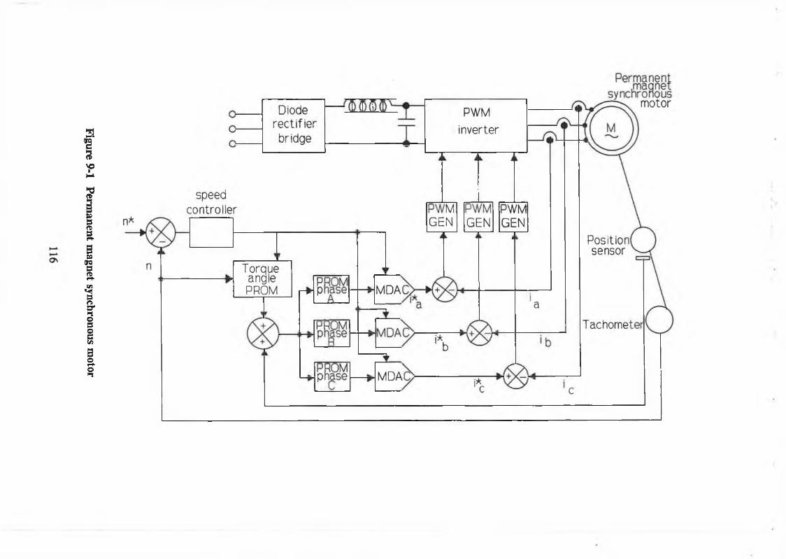
Figure 9-1
Permanent
magnet
synchronous m
otor
References
1-1. M.A.El-Sharkawi, "Development and implementation of high performance
variable tracking control for brushless motors",IEEE Transactions on Energy
Conversion, Vol. 6 N o .l, Mar. 1991. pp 114-119
1-2. Edward C. Lee, "Brushless D.C. A modem approach to variable speed drives",
IEEE 1990 Annual Textile, Fiber and Film Industry Technical Conference, pp
3/1-5.
1-3. Louis-A. Dessaint, Bernard Hebert and Hoang Le-Huy, "An adaptive controller
for a smooth positioning system: analysis and simulation", Conference Record
of the 1988 Industry Applications Society Annual Meeting, pp. 562-5 vol. 1
1-4. M.F. Brosnan and B.Broon, "Closed loop speed control using an A.C.
synchronous motor", IEE proc-B Power Electronics, 1990. pp 373-376
1-5. "AEG AC Servomotors Specifications for the Inland BHT22XX", AEG Inland,
1989.
1-6. A.M.Zikic, "Practical digital control", Halsted Press, 1989.
1-7. M.R. Stojic, "Design of microprocessor-based digital system for DC motor speed
control", IEEE Transaction on Industrial Electronics, Vol. IE-31, no.3, August
1984. pp 243-248
CHAPTER 1:
117
chapter 2:2-1. J.M.D. Murphy and F.G. Turnbull, "power electronic control of AC motors",
Wheaton & Co., 1988.
2-2. P.M. Pelozewshi and U.H. Kunz, "The optimal control of a constrained drive
system with brushless dc motor", IEEE Transaction on Industrial Electronics,
Vol. 3 7 .N0 .5 , Oct. 1990. pp 342-348
2-3. B.K. Bose,"Adjustable speed AC drive systems", IEEE, New York, NY, 1981.
2-4. E.K. Persson and S.Meshket, "Brushless servo system with expanded torque-
speed operating range", Proceeding of Motor-Control Conference, Hannovor,
1985. pp 29-37
2-5. A.C. Stone and M.G. Buckley, "Novel design and control of a trapezoidal back
emf motor: The smooth transition from brush to brushless dc", Proceeding of
Motor-Contral Conference, Hannover, 1985. pp 86-95
CHAPTER 3:
3-1. "AEG AC Servomotors Specifications for the Inland BHT 22XX", AEG Inland,
1989
3-2. A.M.Zikic, "Practical digital control", Halsted Press, 1989.
3-3. P.E. Papamichalis "Digital signal processing application with the TMS320
family, Volume 2", Prentice Hall, 1991.
3-4. Benjamin C. Kuo,"Digital control systems", Holt, Rinehart and Winston, 1980.
3-5. M.R.Stojic, "Design of microprocessor-based digital system for DC motor speed
118
control", TRER Transaction on Industry Electronics, Vol. IE-31 No.3, August
1984. pp 243-248
3-6. Millie R.Stojic, "Microprocessor-based control system",Reidel Publishing
Company, N.K.Sinha, 1986.
3-7. Jiabing Lu "A new adjustable speed system for application on ships", Proceeding
of IMECE’91, 1991. ppl01-108
3-8. Baishi Chen, "Automatic control systems", Jiao Tong Press, China, 1981.
3-9. Guangzhou Chen, "The principles of optimal controller", Journal of Electric
Drive, China, No.4,1973. pp 305-318
3-10. Hugh F. Vanlandingham, "Introduction to digital control system", MacMillan
Publishing Company, 1985.
3-11. KATSUHIKO OGATA " Discrete-time Control System", Prentice-Hall
International Inc., 1987.
CHAPTER 4:
4-1. Frank H.S. & Walter L.G. "A guide to using CSMP-The continuous system
modelling program. " Prentice-Hall, 1976.
4-2. William H.P. & Brian P.F. "Numerical recipes: The art of scientific computing
in C." Cambridge university press, 1989.
4-3. URI M. ASCHER & ROBERT M.M. MATTHEU & ROBERT D. RUSSELL
" Numerical solution of boundary value problems for ordinary differential
equations", PRENTICE-HALL Inc, 1988.
119
4-4. P.D Evans & D Brown "Simulation of brushless DC drives". IEE Proceeding-B,
Vol 137, HB No.5, Sep. 1990. pp299-308
CHAPTER 5:
5-1. JMD MURPHY, FG TURNBULL, "Power Electronic Control of AC Motors",
Pergamon press, 1988.
5-2. P.C SEN, "Principles of Electric Machines and Power Electronics", John Wiley
& Sons, 1988.
5-3. M.G SAY, "Alternating Current Machines",Pitman press, 1976.
5-4. M.G. SAY, E.O TAYLAY, "Direct Current Machines", Pitman press, 1980.
5-5. "BHT 300 Installation and Service Manual", AEG Inland, 1989
5-6. "AEG AC Servomotors Specifications for the Inland BHT 22XX", AEG Inland,
1989.
5-7. "2430A Digital Oscilloscope Operators Manual", Tektronix Inc., 1989.
5-8. P.H MELLOR, D.R TURNER, D. ROBERTS, "Microprocessor based induction
thermal protection", Proceeding of 2nd International Conference EMDA, IEE,
London, 1985. pp 16-20
5-9. P.H MELLOR, D.R TURNER, "Real time prediction of temperatures in an
induction motor using a microprocessor", Electrical Machine Power System,
1988, 13, pp. 333-352.
5-10. P.H MELLOR, D. ROBERTS, D.R TURNER, "Lumped parameter thermal
model for electrical machines of TEFC design", IEE Proceedings-B, Vol. 138,
120
No.5, September 1991. pp205-218
5-11. P.G.A WILSON, "Complete protection of motors under variable load
conditions", Proceeding of Drive/motors/controls, 1983. pp. 172-178
CHAPTER 6:
6-1. Third-Generation TMS320C30 User’s Guide, Texas Instruments, 1988.
6-2. TMS320C30 Assembly Language Tools User’s Guide, Texas Instruments, 1988.
6-3. TMS320C30 C Compiler Reference Guide, Texas Instruments, 1990.
6-4. Panos E. Papamichalis, Digital Signal Processing Applications (volume 2),
Prentice Hall, 1991.
6-5. Microsoft Quick C Compiler programmer’s Guide, Microsoft 1990.
6 -6 . BHT 300 Installation and Service Manual, AEG Inand, 1989.
6-7. Brian W.Kemighan, The C Programming Language, Prentice-Hall, Inc., 1987.
6 -8 . Panos E. Papamichalis, The TMS320C30 Floating-Point Digital Signal
Processor, IEEE proceeding of MICRO, DEC. 1988. ppl3-29
121

APPENDIX AThe servo system model
The brushless servo system used in this project consists of an AEG BHT 2214 brushless
motor and an BHT-300 electronic control system.
The specifications of the brushless driver system are:
Motor:
P=2900 W (rated power);
wm=5000 RPM (maximum operating speed);
M0 =11.3 Nm (continuous torque at 40°C ambient);
Mp=32.1 Nm (peak torque);
Io=21.1 A (rated current at continuous torque);
Ip=63 A (rated current at peak torque);
Vt =300 V (maximum terminal voltage);
Kx=0.536 Nm/A (torque sensitivity);
Kb=56 V/KRPM (back EMF constant);
Rm= 0.30 0 (DC resistance at 25 °C);
Lm= 2.5 mh (inductance);
7^ = 0 . 0 0 1 s (mechanical time constant);
r,=0.0083 s (electrical time constant);
J=0.00098 kg»m 2 (rotor inertia);
F=0.04 Nm/KRPM (viscous damping oo Z source
=0.04/[(1000«2x)/60] =0.000382 Nm*s
rm=J/F=0.536/0.000382=2.57 s
Sensor:
a =0.0435 (10V/230V, speed feedback constant);
A1
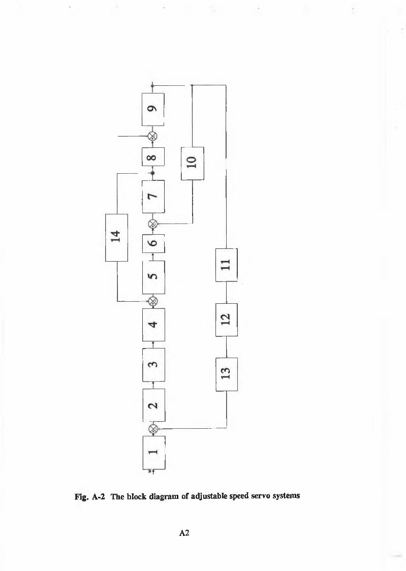
Fig. A-2 The block diagram of adjustable speed servo systems
A2
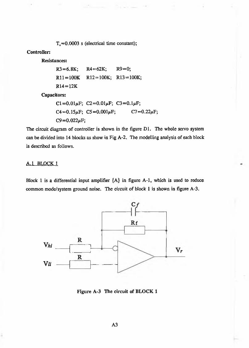
Controller:
Resistances:
R3=6.8K; R4=62K; R9=0;
Rl 1 = 100K R12 = 100K; R13 = 100K;
R14 = 12K
Capacitors:
C1=0.01mF; C2=0.01/xF; C3=0.1/*F;
C4=0.15/xF; C5=0.00lAtF; C7=0.22/iF;
C9 =0.022/zF;
The circuit diagram of controller is shown in the figure D l. The whole servo system
can be divided into 14 blocks as show in Fig A-2. The modelling analysis of each block
is described as follows.
A .l BLOCK 1
Block 1 is a differential input amplifier {A} in figure A -l, which is used to reduce
common mode/system ground noise. The circuit of block 1 is shown in figure A-3.
T,=0.0003 s (electrical time constant);
VW
V/i
Figure A-3 The circuit of BLOCK 1
A3
The transfer function of block 1 is expressed as:
Vz _ Yu - V1AR f R ( A . 1)
R f Cf S + l
( A . 2)
where is the command of the high speed input.
VH is the command of the low speed input.
This equation can be simplified to:
<8
where Kp=Rf/R; T ,=Cf • Rf
A .2 BLOCK 2 and BLOCK 14
Block 2 and block 14 combine a velocity loop in which block 2 is a PI modulator
denotes {C} amplifier and block 14 is a lead modulator in the speed feedback path as
shown in the controller circuit diagram, figure A -l. The speed loop compares a
REQUIRED speed (input voltage) with an ACTUAL speed. The difference or "error"
produces a REQUIRED current signal to current loop. The circuit diagram of block 2
and 14 is shown in figure A-3. The transfer function of the circuit can be expressed as:
VnmKn ( ^ 0 L) (A'3)
where R—10K; T,*,—RQ5; T^—R10C6; and K„—R13/R; Tn—R13C4;
A .3 BLOCK 3 and BLOCK 4
The block 3 and block 4 are the tack filters {D l, D2} in figure A -l, which is used to
eliminate torsional vibrations. Both transfer functions of operational circuits "Dl" and
A4
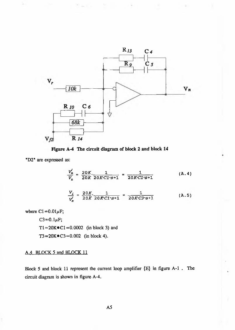
R l 3 C <
Figure A-4 The circuit diagram of block 2 and block 14
"D2" are expressed as:
< = 2 0 K . l = 1 (A.4)VD 2 0 K 2 0 K 'C 1'S +1 2 0 K ‘C 1 ‘S+1
Y l = 20JC. 1 = 1 fAt / 20JT 20J<f*C.2\S+l 2QK'C3‘S+1 v * 7vn
where Cl=0.01/iF;
C 3=0.1/iF;
T1=20K»C 1=0.0002 (in block 3) and
T3=20K>C3=0.002 (in block 4).
A.4 BLOCK 5 and BLOCK 11
Block 5 and block 11 represent the current loop amplifier {E} in figure A -l . The
circuit diagram is shown in figure A-4.
A5
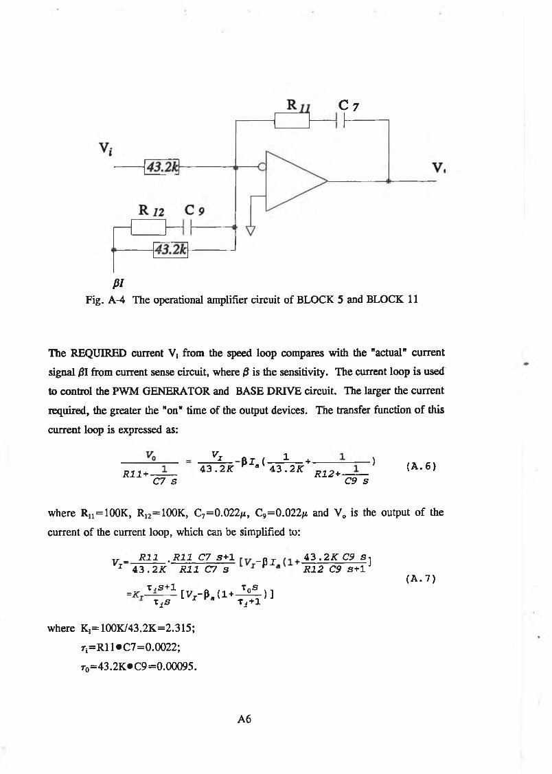
C 7k
PIFig. A-4 The operational amplifier circuit of BLOCK 5 and BLOCK 11
The REQUIRED current V; from the speed loop compares with the "actual" current
signal 01 from current sense circuit, where /? is the sensitivity. The current loop is used
to control the PWM GENERATOR and BASE DRIVE circuit. The larger the current
required, the greater the "on" time of the output devices. The transfer function of this
current loop is expressed as:
R11 + -— Yl - R j ( 1— +43 . 2K K a 43 . 2K ■)
C7 SR12+
( A . 6)C9 S
where Rn = 100K, R12=100K, C7 =0.022/x, C9 =0.022/x and V0 is the output of the
current of the current loop, which can be simplified to:
v _ R l l . R l l C7 S + l _ p J . 43 . 2 K C9 S jJ 43 . 2 K R l l C7 3 R 12 C9 s + l
=KTX jS + 1
r iS [VJ - p a ( l + To3
Tj+ 1
( A . 7)
)]
where K,= 100K/43.2K=2.315;
Ti=Rl 1 *C7 =0.0022;
t0 =43.2K*C9 =0.00095.
A6
The coefficient /3 needs to be calculated. For BHT 2214 motor, the current sensitivity
is module D (10 A/V) [1]. In the torque-speed characteristic diagram, the maximum
torque is 32.1 Nm, so the maximum current which is T/Kt= 32. 1/0.536=59.9 A. The
maximum voltage of the controller is 10 V. Therefore ,
0 = 1 0 V/(59.9/10)-1.67
A.5 The transfer function of BLOCK 6
Block 6 represents the PWM generator and invertor. They can be approximately
modeled to a gain. The input of the PWM is + /- 10V and DC output of the inverter
is + /- 300V. So the gain is: KA = 300/10 =30
A . 6 BLOCK 7. Block 8 . Block 9 and Block 10
The brushless DC motor can be expressed as:
+ * * a+Vb (A . 8 )
( A . 9)
( A . 10)
( A . 11)
I A(a)1
R ( A . 12)VA(S)-VB(S) v s + i
From equation (A.8 ), the transfer function of block 7 can be modeled to equation
(A. 12): where re=L/R (electrical time constant).
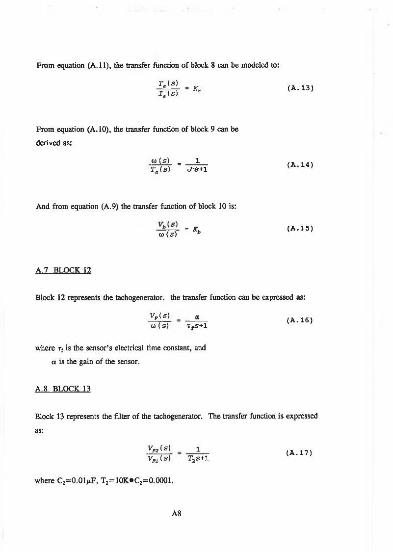
From equation (A. 11), the transfer function of block 8 can be modeled to:
T* (S) = K t (A . 13)I J s )
From equation (A. 10), the transfer function of block 9 can be
derived as:
<■><*> = _ J L _ (A 14)T A s ) iJ 's+ l
And from equation (A.9) the transfer function of block 10 is:
- Kb (A . 1 5 )co <s) a
A.7 BLOCK 12
Block 12 represents the tachogenerator. the transfer function can be expressed as:
( A . 16)VF {s)W(s) Tf S + l
where rf is the sensor’s electrical time constant, and
a is the gain of the sensor.
A.8 BLOCK 13
Block 13 represents the filter of the tachogenerator. The transfer function is expressed
as:
Vp2 ( a )Vr i {s) T2s +1
where C2=0.01/zF, T2 = 1 OK»C2=0.0001.
A8
( A . 1 7 )

A.9 The whole system modelThrough out the analysis of each block, we can obtain the block diagram o f the total
servo system model as shown in figure A-5, which is used to design the speed
controller.
A9
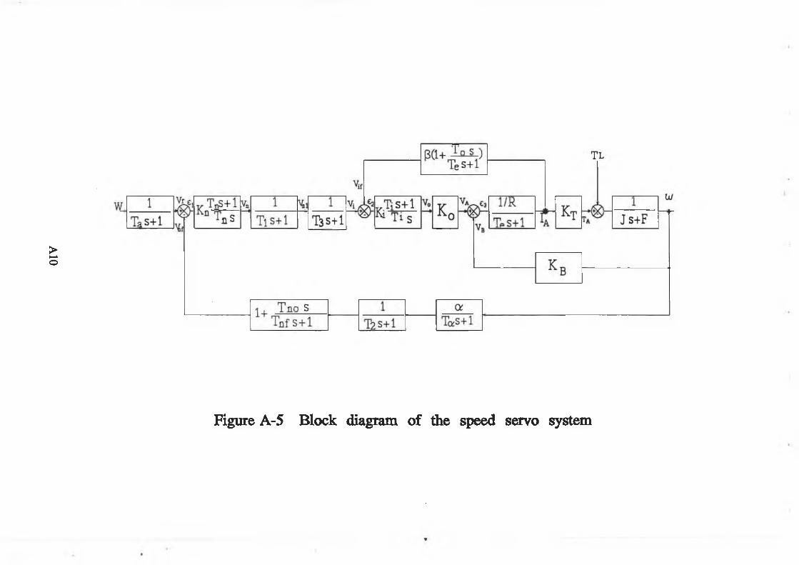
AIO
Figure A-5 Block diagram of the speed servo system
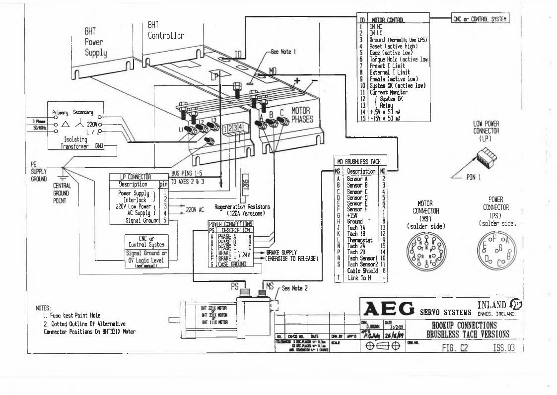
BHTC o n t r o l l e r
IN HI IN LOG round ( t o n a l l y Uss LP5 ) Reset (active nigh)Cage (active low)Torque Hold (active low Preset I Liiit External I Unit Enable (active low) Systea OK (active low) Current Monitor / Systea OK I Relay
+15V • 50 bA -15V t 50 rA
P r i* a ru Secondarli
"° I o -o A A 2 2 0 V o -° L / IP“
Isolating Transformer GND
HD BRUSHLESS TACHDescription Sensor A Sensor B Sensor C Sensor D Sensor E Sensor F +15V Ground Tech 1A Tach IB Theraostat Tach 2A Tach 2B Tach Sensorl Tach Sensor2 Cable Shield Link To H
Description Power Supply }
Interlock J 220V Low Power \ AC Supply / Signal Ground
POWERCONNECTOR
(PS)(solder side)
MOTOR CONNECTOR (MS) (solder side)
Regeneration Resistors (120A Versions)
POWER CONNECTION^ PS1 OESmiPTION A PHASE A AB PHASES BC PHASE C CE BRAKE -1 24VF BRAKE + )J L CASE
CNC or Control SystemBRAKE SUPPLY (ENERGISE TO RELEASE)
I N L A N D (JbSERVO SYSTEMS ENNIS. IRELAND1. Fuse test Point Hole
2. Dotted Outline Of Alternative Connector Positions On BHT331X Motor 21/M8
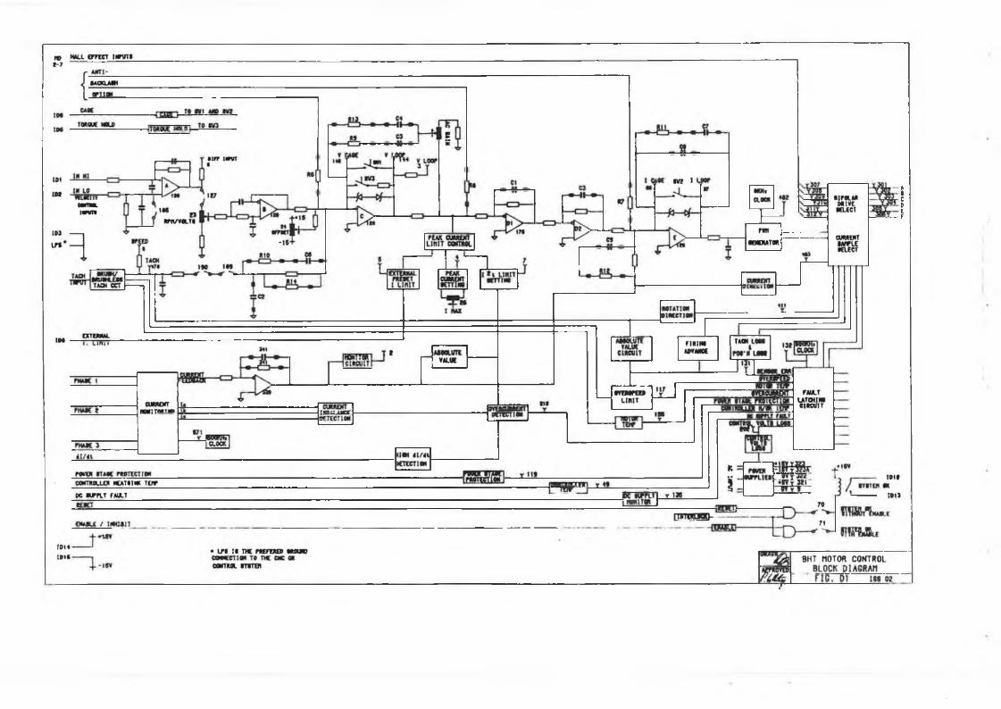
7
Or,/Off
IT'9VB o t t e r y
R e v e r 9 l n g
- S i l t c h
BATTERYBOX
*5 - 1 O K
S p e e d
R e f e r e n c e
Close to EN A BL E [Close to CAGE f"*"
Close to TORQUE HOLD r ^ ^ Y Ô V
I D C o n n e c t o r
I
BHT C o n t r o 11er
“ 7 . ^ G r o u n d S c r e e n
- - o t B H T
P o r t a b l e B a t t e r y Box - BHT C o n n e c t i o n s
P « « « r 1 0 V A
S e t t « h l 0 0 w A 2 4 0 V
» ■ ------------1— 1
A . C . 220V * -
H o l n e
S u p p l y
« ------------------------------------------
110V • -
-------------------------------
a
, - 1 5 V
U t * O n e I
C o m p l e t • ^
C l r o u l t \
P e r A x l e |
II
Close to ENABLE [
c j lose to CAGEIlN Close to T O R Q U E HOLD
Figure D4 Mains P o w e r e d B a t t e r y Box - BHT C o n n e c t i o n s
APPENDIX B
B-I. The simulation program for DESIGN I
^ * * * * * * * * * * * * * * * * * * * * * * * * * * * * * * * * * * * * * * * * * * * * * * * * * * * * * * * * * *
* Simulation program for disign I speed controller ** ** Author: Jiabing Lu ************************************************************/
^include <stdlib.h>^include <stdio.h>#include <math.h>
#define KT 0.536 /* V/rpm * /^define KB 0.056 /* Nm/A */^define N 10
float w,ki,kp,kd; int n;
char name[1 0 ];
m ainO
{float x[18]={0.0}; float error[5]={0.0}; float xin[1 2 ]= { 0 .0 },tran[1 2 ]= { 0 .0 }; float h = 0 .0 0 0 1 ;float time= 0 .0 , output= 0 .0 , current= 0 .0 ; int j,i,m,l;
/♦parameter of digital controller*/
float ul = 0 .0 ,erl = 0 .0 ,u= 0 .0 ,er= 0 .0 ,in = 0 .0 , w l = 0 .0 ;
FILE *dat;
B1
inputnameO;
/♦numbers of output points ♦/
m=40;dat= fopen(name," w"); for(j=0 ;j<m;j + + ){
fprintf(dat,"\n%f %f % f % {” ,time,x[9],output,power); for(i =0;i < 500;i 4-+){
/********** OPTIMIZING DIGITAL CONTROLLER **********/
er=wl-in;u=ul+5.3348*(er-0.999335*erl);u l= u;erl =er;x[2 ]=u;
/♦sample time is T=n*h*/
for(l=0;1 < N;1 + + ){
/******* CONTINUOUS TIME PARTS *******/
inputO;
tim e+=h;/♦block 4 =x[4]/x[2] = l/(l+0 .002s) filter ♦/
block(x[2], 1.0,0.002,1.0,0.0, h,xin[3],&tran[3],&x[4]); xin[3]=tran[3];
/♦* current loop ♦♦/
error[2]= x[4]-x[ 16];
/♦ Ki=2.315 ♦/
x[5]=2.315*error[2];
/♦block 5 = x[6]/x[5] = 0.0022s/(l+0.0022s) ♦/block(x[5],0.0,0.0022,1.0,0.0022, h,xin[4],&tran[4],&x[6]);
B2
x[7]=60.0#x[6];
error[3] =x[7]-x[l 1];
/♦block 7 = x[9]/error[3] = l/(0.3 + 0.0025s) ♦/
block(error[3] ,0.3,0.0025,1.0,0.0,h ,xin[5],&tran [5], &x [9]); xin[5]=tran[5];
/♦block 8 = x[9]/x[10] = KT =0.536 , current to torque*/
x[10]=KT#x[9];
error[4] =x[10]-load;
/♦block 9 = output/error[4] = (1/F)/(1+J/F s) ♦/
block(error[4], 1.0,24.5,25000.0,0.0,h,xin[6],&tran[6],&output); xin[6 ]=tran[6 ];
/♦block 10 = feedback e.m .f constant = KB = 0.056 (V/rpm) */
x[l 1] =KB#output;
/♦block 1 1 = speed feedback constant = 0 . 0 0 1 ♦/
x[1 2 ] = 0 . 0 0 1 ♦output;
/♦♦ block 12 and 13 is speed feedback filter ♦♦/
/♦block 12 = speed feedback =1/(1 + .0003s) ♦/
block(x[12], 1.0,0.0003,1.0,0.0, h,xin[7] ,&tran[7],&x[13]); xin[7]=tran[7];
/♦block 1 3 = l / ( l + 0 .0 0 1 s) ♦/block(x[13], 1.0,0.001,1.0,0.0, h,xin[8],&tran[8],&x[14]); xin[8 ]=tran[8 ];
/♦ speed feedback to digital controller ♦/
b2=x[14];
/♦bklock 14 = current feedback filter = (1+0.00315s)/(l+0.0022s); b=0.1 *1
xin[4]=tran[4];
/♦block 6 = x[7]\x[6] = ko=60.0*/
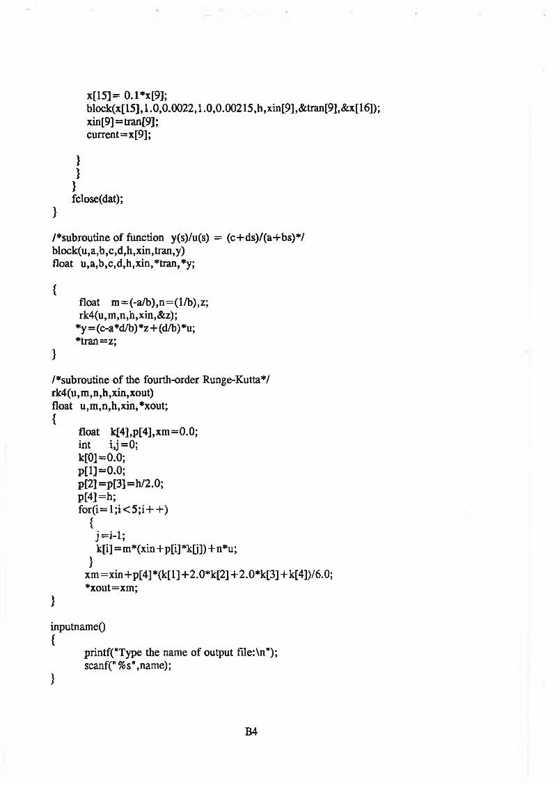
x[15]= 0.1*x[9];block(x[15], 1.0,0.0022,1.0,0.00215, h,xin[9],«fetran[9],&x[16]);xin[9]=tran[9];current=x[9];
}}}fclose(dat);
}
/♦subroutine of function y(s)/u(s) = (c+ds)/(a+bs)*/block(u,a,b,c,d,h,xin,tran,y)float u,a,b,c,d,h,xin,*tran,*y;
{float m =(-a/b),n=(l/b),z; rk4(u,m,n,h,xin,&z);
*y= (c-a*d/b) *z+ (d/b) *u;*tran=z;
}
/♦subroutine of the fourth-order Runge-Kutta*/rk4(u,m,n,h,xin,xout)float u,m,n,h,xin,*xout;{
float k[4],p[4],xm=0.0;int i,j = 0 ;k[0 ] = 0 .0 ;p [ l]= 0 .0 ;p[2]=p[3]=h/2.0;p[4]=h;fo r (i= l; i< 5 ;i+ + )
{j= i- l;k[i] = m*(xin+p[i] *k[j])+ n*u;
}xm =xin+p[4]*(k[l] +2.0*k[2] +2.0*k[3]+k[4])/6.0; *xout=xm;
}
inputnameO{
printf("Type the name of output file:\n"); scanf("%s",name);
}
B4

B-II. The simulation program for DESIGN II
^ * * * * * * * * * * * * * * * * * * * * * * * * * * * * * * * * * * * * * * * * * * * * * * * * * * * * * * * * * * *
♦ Simulation program for disign n speed controller ** ** Author: Jiabing Lu ************************************************************/
^include <stdlib.h> #include <stdio.h> ^include <math.h>
^define KP 18^define KI 0 . 1
^define KD 55#define KT 0.536 /♦ V/rpm ♦/^define KB 0.056 /♦N m /A ♦/^define N 1 0
char name[1 0 ];
mainO
float x[18]={0.0};float error[5] = {0.0};float xin[1 2 ] = { 0 .0 },tran[1 2 ] = {0 .0 };float h- 0 .0 0 0 1 ;float output=0 .0 ,current= 0 .0 ;int
/♦parameter of digital controller*/
float bl = 0 .0 ,b2 = 0 .0 ,ul = 0 .0 ,u2 = 0 .0 ,e = 0 .0 ,u = 0 .0 ;
FILE *dat;
inputnameO;
/♦numbers of output points */
m=40;dat=fopen(name,"w"); for(j = 0 ;j < m;j + + ){
B5
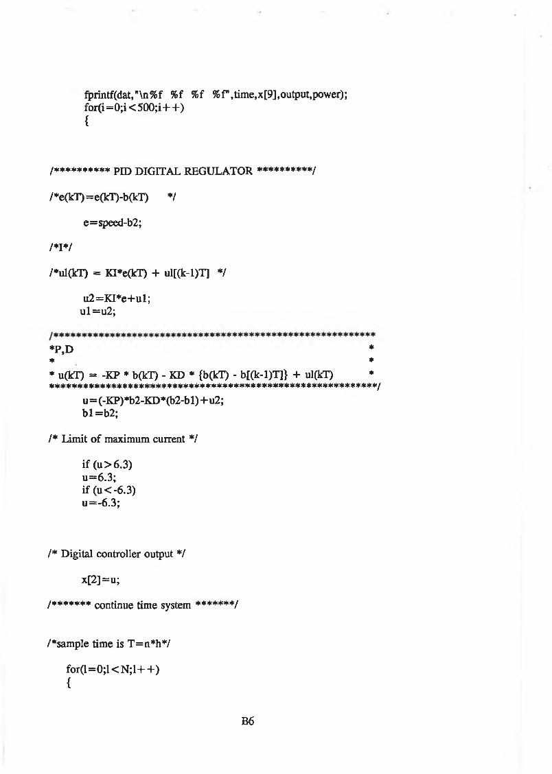
fprintfCdat,"\n%f %f %f %f",time,x[9],output,power); for(i=0;i < 500;i+ +){
/********** PID DIGITAL REGULATOR **********/
/*e(kT)=e(kT)-b(kT) */
e = speed-b2 ;
1*1*1
/*ul(kT) = KI*e(kT) + ul[(k-l)T] * /
u2=KI*e+ul;u l= u 2 ;
*P,D ** ** u(kT) = -KP * b(kT) - KD * (b(kT) - b[(k-l)T]} + ul(kT) ************************************************************/
u=(-KP)*b2-KD*(b2-bl)+u2; b l= b 2 ;
/ * Limit o f maximum current */
if (u>6.3) u=6.3; if (u<-6.3) u=-6.3;
/* Digital controller output * /
x[2 ]=u;
/ * * * * * * * continue time system * * * * * * * /
/♦sample time is T=n*h*/
fo r (l= 0 ;l< N ;l+ + ){
B6
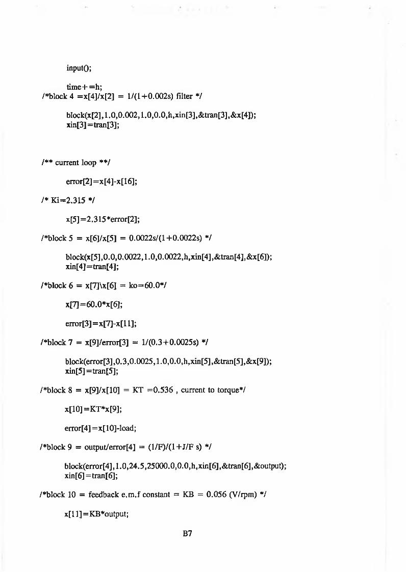
inputo ;
time+ =h;/♦block 4 =x[4]/x[2] = l/(l+ 0 .002s) filter ♦/
block(x[2], 1.0,0.002,1.0,0.0, h,xin[3],&tran[3],&x[4]); xin[3]=tran[3];
/** current loop **/
error[2] =x[4]-x[16];
/♦ Ki=2.315 ♦/
X [5] = 2.315 ♦error[2] ;
/♦block 5 = x[6]/x[5] = 0.0022s/(l+0.0022s) ♦/
block(x[5],0.0,0.0022,1.0,0.0022, h,xin[4],&tran[4],&x[6]); xin[4]=tran[4];
/♦block 6 = x[7]\x[6] = ko=60.0#/
x[7]=60.0#x[6];
error[3] =x[7]-x[l 1];
/♦block 7 = x[9]/error[3] = l/(0.3 +0.0025s) */
block(error[3],0.3,0.0025,1.0,0.0,h,xin[5],&tran[5],&x[9]); xin[5] =tran[5];
/♦block 8 = x[9]/x[10] = KT =0.536 , current to torque*/
x[10]=KT+x[9];
error[4] =x[10]-load;
/♦block 9 = output/error[4] = (1/F)/(1 +J/F s) ♦/
block(error[4], 1.0,24.5,25000.0,0.0, h,xin[6 ],&tran[6 ],&output); xin[6 ]=tran[6 j;
/♦block 10 = feedback e.m .f constant = KB = 0.056 (V/rpm) ♦/
x [ll]= K B #output;
B7
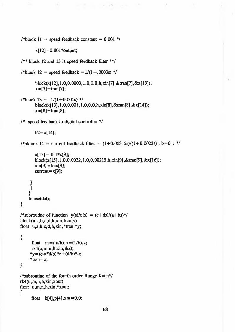
x[1 2 ] = 0 . 0 0 1 ♦output;
/♦♦ block 12 and 13 is speed feedback filter ♦♦/
/♦block 12 = speed feedback = 1 /(1 + .0003s) ♦/
block(x[12], 1.0,0.0003,1.0,0.0, h,xin[7],&tran[7],&x[13]); xin[7]=tran[7];
/♦block 13 = l/(l+ 0 .001s) ♦/block(x[13], 1.0,0.001,1.0,0.0, h,xin[8],&tran[8],&x[14]); xin[8 ]=tran[8 ];
/♦ speed feedback to digital controller ♦/
b2=x[14];
/♦bklock 14 = current feedback filter = (1 +0.00315s)/(l+ 0 .0022s); b=0.1 ♦/
x[15]= 0.1M 9];block(x[15], 1.0,0.0022,1.0,0.00215,h,xin[9],&tran[9],&x[16]);xin[9]=tran[9];current=x[9];
}}}fclose(dat);
}
/♦subroutine of function y(s)/u(s) = (c+ds)/(a+bs)*/block(u,a,b,c,d,h,xin,tran,y)float u,a,b,c,d,h,xin,+tran,*y;
{float m =(-a/b),n=(l/b),z; rk4(u,m,n,h,xin,&z);
♦y= (c-a*d/b) ♦z+ (d/b) *u;♦tran=z;
}
/♦subroutine of the fourth-order Runge-Kutta#/rk4(u,m,n,h,xin,xout)float u,m,n,h,xin,#xout;{
float k[4],p[4],xm=0.0;
/♦block 11 = speed feedback constant = 0.001 ♦/
B8
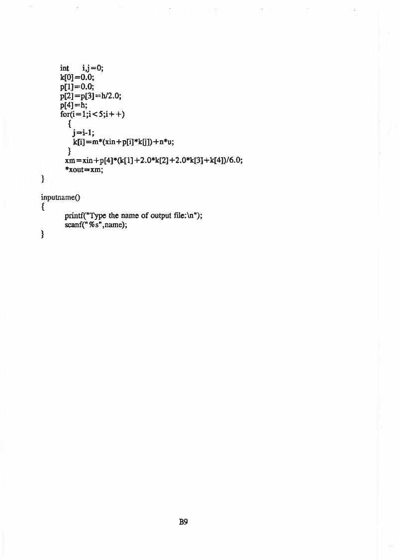
int i,j =0;k[0]=0.0;p [l]= 0 .0 ;p[2]=p[3]=h/2.0;p[4]=h;fo r ( i= l; i< 5 ; i+ + )
{j= i- i;k[i] =m *(xin+p[i]*k[j])+n*u;
}xm =xin+p[4]*(k[l] +2.0*k[2] +2.0*k[3]+k[4])/6.0; *xout=xm;
inputnameO{
printf("Type the name of output file:\n"); scanf("%s",name);
}
B9
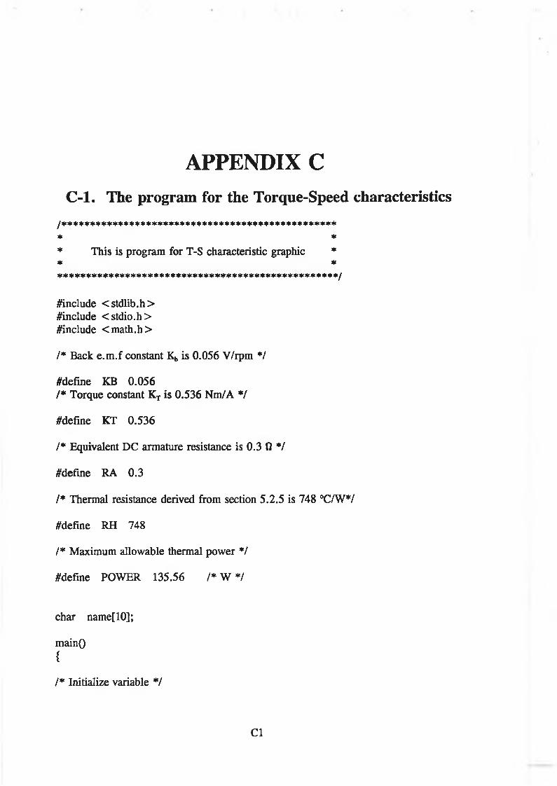
APPENDIX CC -l. The program for the Torque-Speed characteristics
/I************************************************** ** This is program for T-S characteristic graphic ** * I**:**************!*:***************************:******/
¿include <stdlib.h>¿include <stdio.h>¿include <math.h>
/* Back e.m .f constant Kb is 0.056 V/rpm * /
¿define KB 0.056/ * Torque constant Kx is 0.536 Nm/A */
¿define KT 0.536
/* Equivalent DC armature resistance is 0.3 t) */
¿define RA 0.3
/* Thermal resistance derived from section 5.2.5 is 748 °CAV*/
¿define RH 748
I * Maximum allowable thermal power * /
¿define POWER 135.56 /* W */
char name[1 0 ];
mainO{
/ * Initialize variable * /
C l
float torque=0 .0 ; float speed=5000.0; float current= 0 .0 ; float em f=0 .0 ; float y = 0 .0 ; int n;FILE *dat; inputO;dat= fopen(name," w");
for(n=0;n < 44;n+ + ){fprintf(dat,"%f %f\n",torque,speed);
/* Increase current 0.5 A each time */
current=current+0.5;
/* Torque = I x KT */
torque=current*KT;
/* E2 = ( P - F x R J x R f c
y = (POWER-current *current *RA) *RH;
/* E2 ^ 0*/
if(y < 0 .0 )y = 0 .0 ;emf=sqrt(y);
/* Speed = E/Kb */
speed=emf/KB;
/* Maximum speed is 5000 rpm *1
if(speed> 5000.0) speed=5000.0;}
fclose(dat);}inputO{
printf("Type the name of output file:\nH); scanf("%s",name);
}
C l
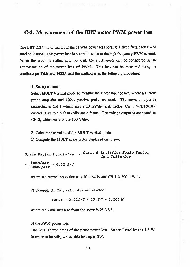
C-2. Measurement of the BHT motor PWM power loss
The BHT 2214 motor has a constant PWM power loss because a fixed frequency PWM
method is used. This power loss is a core loss due to the high frequency PWM current.
When the motor is stalled with no load, the input power can be considered as an
approximation of the power loss of PWM. This loss can be measured using an
oscilloscope Tektronix 2430A and the method is as the following procedure:
1. Set up channels
Select MULT Vertical mode to measure the motor input power, where a current
probe amplifier and 100 x passive probe are used. The current output is
connected to CH 1 which uses a 10 mV/div scale factor. CH 1 VOLTS/DIV
control is set to a 500 mV/div scale factor. The voltage output is connected to
CH 2, which scale is the 100 V/div.
2. Calculate the value of the MULT vertical mode
1) Compute the MULT scale factor displayed on screen:
_ , „ , ,, , , , , , C u r r e n t A m p l i f i e r S c a l e F a c t o rS c a l e F a c t o r M u l t i p l i e r = ---------------------------„ -, ---------------------CH 1 V o l t s / D i v
= , 10 r o A /d iv = 0 02 A / v 5 0 0 m V / d i v
where the current scale factor is 10 mA/div and CH 1 is 500 mV/div.
2) Compute the RMS value of power waveform
P o w e r = 0 . 0 2 A / V x 2 5 . 3 V 2 = 0 . 5 0 6 W
where the value measure from the scope is 25.3 V2.
3) the PWM power loss
This loss is three times of the phase power loss. So the PWM loss is 1.5 W.
In order to be safe, we set this loss up to 2W.
C3
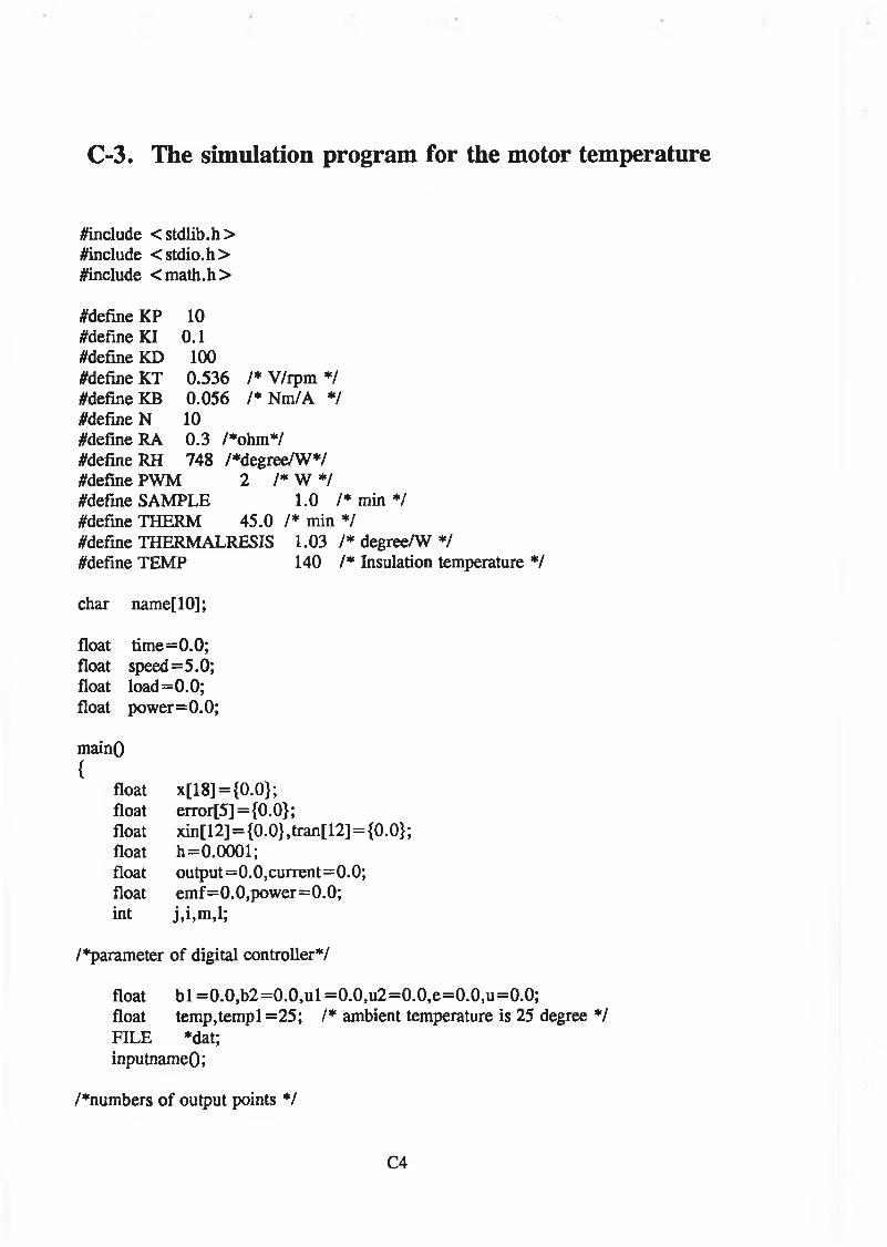
C-3. The simulation program for the motor temperature
¿include <stdlib.h>¿include <stdio.h>¿include <math.h>
¿define KP 10¿define KI 0.1¿define KD 100¿define KT 0.536 /♦ V/rpm */¿define KB 0.056 /* Nm/A ♦/¿define N 10¿define RA 0.3 /*ohm*/¿define RH 748 /♦degree/W*/¿define PWM 2 /* W */¿define SAMPLE 1.0 /* min */¿define THERM 45.0 /* min ♦/¿define THERMALRESIS 1.03 /* degree/W */¿define TEMP 140 /* Insulation temperature */
char name[1 0 ];
float time=0 .0 ; float speed=5.0; float load= 0 .0 ; float power= 0 .0 ;
mainO{
float x[18] = {0 .0 };float error[5] = {0.0};float xin[1 2 ] = {0 .0 },tran[1 2 ] = {0 .0 };float h = 0 .0 0 0 1 ;float output=0 .0 ,current=0 .0 ;float emf= 0 .0 ,power= 0 .0 ;int j,i,m ,l;
/♦parameter of digital controller*/
float b l = 0 .0 ,b2 = 0 .0 ,ul = 0 .0 ,u2 = 0 .0 ,e = 0 .0 ,u = 0 .0 ;float temp,tempi =25; /* ambient temperature is 25 degree */FILE *dat; inputnameO;
/♦numbers of output points */
C4
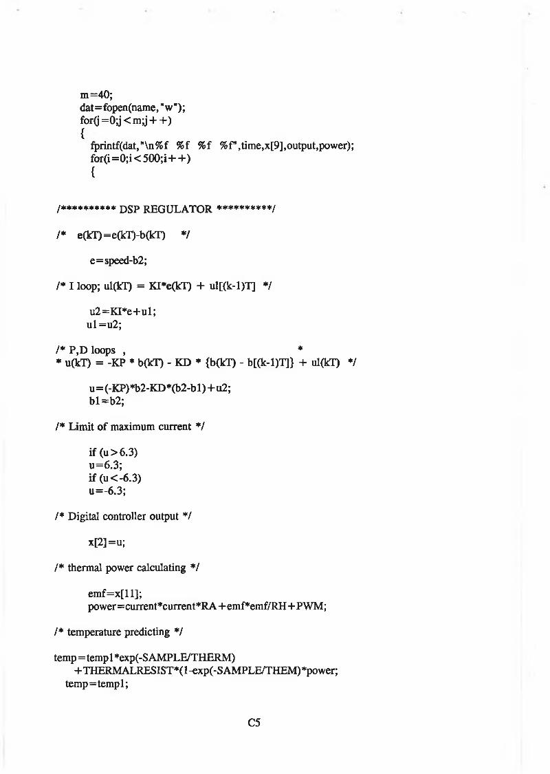
m=40;dat=fopen(name, "w"); for(j = 0 ;j < m;j + + ){
fprintf(dat,"\n%f % f %f %f",time,x[9],output,power); for(i= 0;i< 500;i+ + ){
/********** j)5 p REGULATOR **********/
/* e(kT)=e(kT)-b(kT) * /
e=speed-b2 ;
/* I loop; ul(kT) = KI*e(kT) + ul[(k-l)T] */
u2=KI*e+ul;u l= u 2 ;
/* P,D loops , ** u(kT) = -KP * b(kT) - KD * {b(kT) - b[(k-l)T]> + ul(kT) * /
u= (-KP) *b2-KD *(b2-b 1 ) + u2 ; bl =b2 ;
/* Limit of maximum current * /
if (u>6.3) u=6.3; if (u<-6.3) u=-6.3;
/* Digital controller output */
x[2 ]=u;
/ * thermal power calculating */
em f=x[ll];power= current*current*RA+ em fem f/RH+ PWM ;
/ * temperature predicting */
temp= temp 1 *exp(-S AMPLE/THERM)+ THERMALRESIST*(1-exp (-SAMPLE/THEM) *power;
temp= tempi;
C5
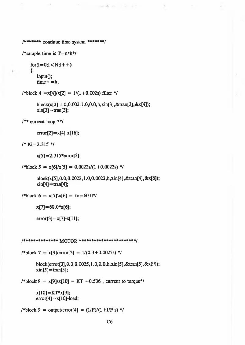
/♦sample time is T=n*h*/
fo r (l= 0 ;l< N ;l+ + ){
inputO; time+ =h;
/♦block 4 =x[4]/x[2] = l/(l+ 0 .002s) filter ♦/
block(x[2], 1.0,0.002,1.0,0.0, h,xin[3],&tran[3],&x[4]); xin[3] =tran[3];
/*♦ current loop ♦♦/
error[2] =x[4]-x[16];
/♦ Ki=2.315 ♦/
x[5] =2.315*error[2];
/♦block 5 = x[6]/x[5] = 0.0022s/(l+0.0022s) ♦/
block(x[5],0.0,0.0022,1.0,0.0022, h,xin[4],&tran[4],&x[6]); xin[4]=tran[4];
/♦block 6 = x[7]\x[6] = ko=60.0V
x[7]=60.0#x[6];
error[3] = x[7]-x[ 11];
!#>************* MOTOR ***********************/
/♦block 7 = x[9]/error[3] = l/(0.3+0.0025s) ♦/
block(error[3],0.3,0.0025,1.0,0.0,h,xin[5],&tran[5],&x[9]); xin[5]=tran[5];
/♦block 8 = x[9]/x[10] = KT =0.536 , current to torque^/
x[10]=KT+x[9]; error[4] =x[10]-load;
/♦block 9 = output/error[4] = (1/F)/(1+J/F s) ♦/
/******* continue time system *******/
C6
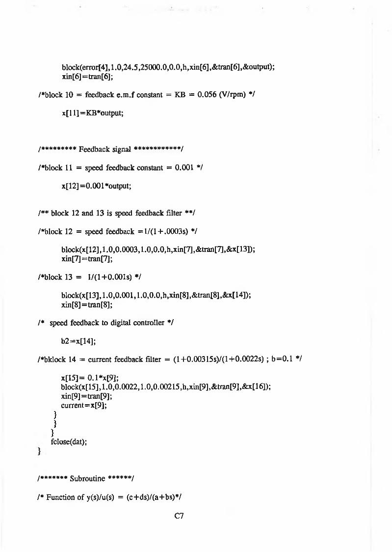
block(error[4], 1.0,24.5,25000.0,0.0, h,xin[6 ],&tran[6 ],&output); xin[6 ]=tran[6 ];
/♦block 10 = feedback e.m.f constant = KB = 0.056 (V/rpm) ♦/
x[ll]=KB*output;
/********* Feedback signal ♦***********/
/♦block 1 1 = speed feedback constant = 0 . 0 0 1 */
x[1 2 ] = 0 . 0 0 1 ♦output;
/♦♦ block 12 and 13 is speed feedback filter ♦♦/
/♦block 12 = speed feedback =1/(1 + .0003s) ♦/
block(x[12],1.0,0.0003,1.0,0.0,h,xin[7],&tran[7],&x[13]); xin[7]=tran[7];
/♦block 13 = 1/(1 +0.001s) ♦/
block(x[13], 1.0,0.001,1.0,0.0,h,xin[8] ,&tran[8 ] ,&x[14]); xin[8 ]=tran[8 ];
/♦ speed feedback to digital controller ♦/
b2=x[14];
/♦bklock 14 = current feedback filter = (l+0.00315s)/(l+0.0022s) ; b=0.1 */
x[15]= 0.1*x[9];block(x[15],1.0,0.0022,1.0,0.00215,h,xin[9],&tran[9],&x[16]);xin[9]=tran[9];current=x[9];
}}}fclose(dat);
/ * * * * * * * Subroutine ******/
/♦ Function of y(s)/u(s) = (c+ds)/(a+bs)#/
C7
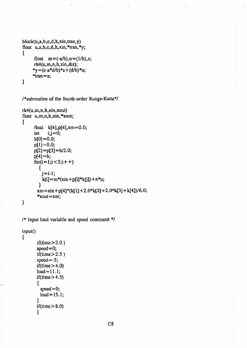
block(u,a,b,c,d,h,xin,tran,y) float u,a,b,c,d,h,xin,*tran,*y;{
float m =(-a/b),n=(l/b),z; rk4(u,m,n,h,xin,&z);
* y = (c-a*d/b)*z+(d/b)*u; *tran=z;
}
/♦subroutine of the fourth-order Runge-Kutta*/
rk4(u,m,n,h,xin,xout) float u,m,n,h,xin,*xout;{
float k[4],p[4],xm=0.0;int i j = 0 ;k[0 ] = 0 .0 ;p[l] = 0 .0 ;p[2]=p[3]=h/2.0;p[4]=h;fo r (i= l; i< 5 ;i+ + )
{j= i- l;k[i]=m*(xin+p[i]*k[j])4-n*u;
}xm=xin+p[4]*(k[l] +2.0*k[2] +2.0*k[3] +k[4])/6.0; *xout=xm;
}
/* Input load variable and speed command * /
inputO{
if(tim e>2 .0 ) speed= 0 ; if(tim e>2.5) speed=-5; if(time>4.0) load= 1 1 . 1 ; if(time>4.5){
speed = 0 ; load=15.1;
}if(tim e>8 .0 ){
C8

load =5.2; speed=4;
}if(time> 1 2 ) load = 1 0 ; if(time> 16) load = 0 ; if(time> 18) load= 1 2 ;
}
/* Input a name of output file * /
inputnameO{
printf("Type the name of output file:\n"); scanf("%s",name);
}
C9
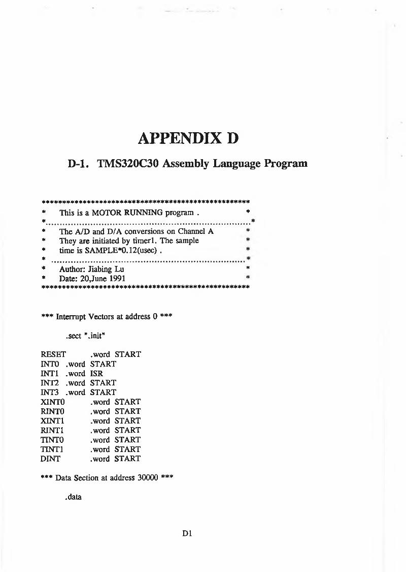
APPENDIX DD -l. TMS320C30 Assembly Language Program
************************************************** This is a MOTOR RUNNING program . *
The A/D and D/A conversions on Channel A They are initiated by timerl. The sample time is SAMPLE*0.12(usec) .
Author: Jiabing Lu *Date: 20,June 1991 *
* * * * * * * * * * * * * * * * * * * * * * * * * * * * * * * * * * * * * * * * * * * * * * * * * *
*** Interrupt Vectors at address 0 ***
.sect ".init"
RESET .word STARTINTO .word START INTI .word ISR INT2 .word START INT3 .word START X1NT0 .word STARTRINTO .word STARTXINT1 .word STARTRINT1 .word STARTTINTO .word STARTTINT1 .word STARTDINT .word START
*** Data Section at address 30000 ***
.data
D1
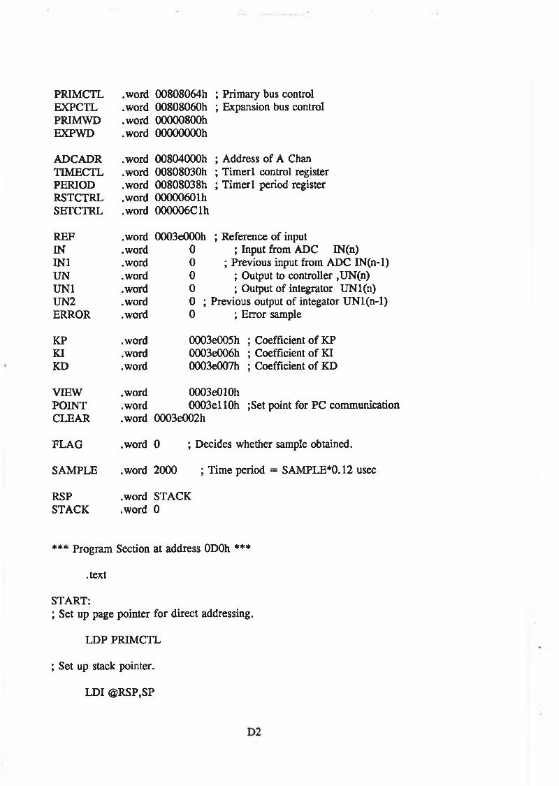
PRIMCTL .word 00808064h ; Primary bus controlEXPCTL .word 00808060h ; Expansion bus controlPRIMWD .word 00000800hEXPWD .word OOOOOOOOh
ADC ADR .word 00804000h ; Address of A ChanTIMECTL .word 00808030h ; Timer 1 control registerPERIOD .word 00808038h ; Timerl period registerRSTCTRL .word 0000060lhSETCTRL .word 000006Clh
REF .word 0003e000h ; Reference of inputIN .word 0 ; Input from ADC IN(n)INI .word 0 ; Previous input from ADC IN(n-l)UN .word 0 ; Output to controller ,UN(n)UNI .word 0 ; Output of integrator UNl(n)UN2 .word 0 ; Previous output of integator UNl(n-l)ERROR .word 0 ; Error sample
KP .word 0003e005h ; Coefficient of KPKI .word 0003e006h ; Coefficient of KIKD .word 0003e007h ; Coefficient of KD
VIEW .word 0003e010hPOINT .word 0003ell0h ; Set point for PC communicationCLEAR .word 0003e002h
FLAG .word 0 ; Decides whether sample obtained.
SAMPLE .word 2000 ; Time period = SAMPLE*0.12 usee
RSP .word STACKSTACK .word 0
*** Program Section at address ODOh ***
.text
START:; Set up page pointer for direct addressing.
LDP PRIMCTL
; Set up stack pointer.
LDI @RSP,SP
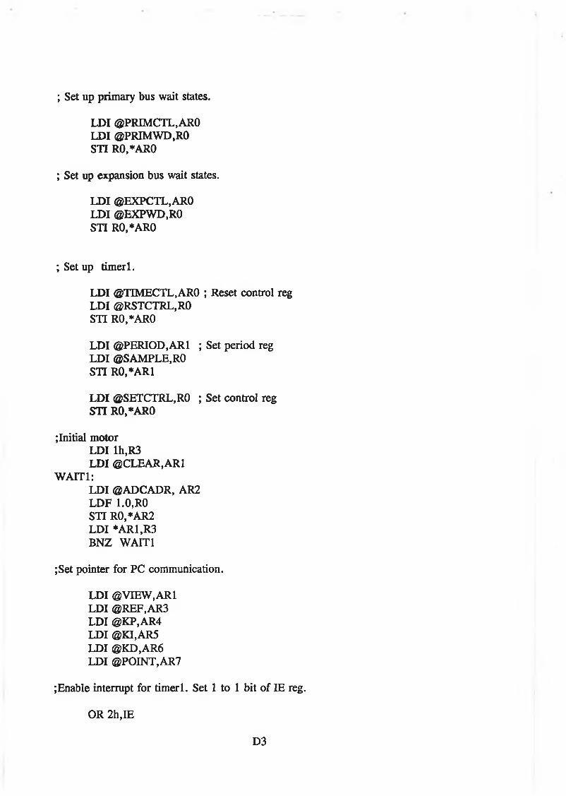
; Set up primary bus wait states.
LDI @PRIMCTL,ARO LDI @PRIMWD,RO SIT RO,*ARO
; Set up expansion bus wait states.
LDI @EXPCTL,ARO LDI ©EXPWD.RO STI R0,*AR0
; Set up timer 1.
LDI ©TEMECTL, ARO ; Reset control reg LDI @RSTCTRL,RO STI R0,*AR0
LDI ©PERIOD, AR1 ; Set period reg LDI ©SAMPLE,RO STI R0,*AR1
LDI ©SETCTRL.RO ; Set control reg STI R0,*AR0
;Initial motorLDI lh,R3 LDI ©CLEAR, AR1
WAIT1:LDI ©ADCADR, AR2 LDF 1.0, R0 STI R0,*AR2 LDI *AR1,R3 BNZ WAIT!
;Set pointer for PC communication.
LDI @VIEW,AR1 LDI @REF,AR3 LDI @KP,AR4 LDI @KI,AR5 LDI @KD,AR6
LDI ©POINT, AR7
;Enable interrupt for timerl. Set 1 to 1 bit of IE reg.
OR 2h,IE
D3
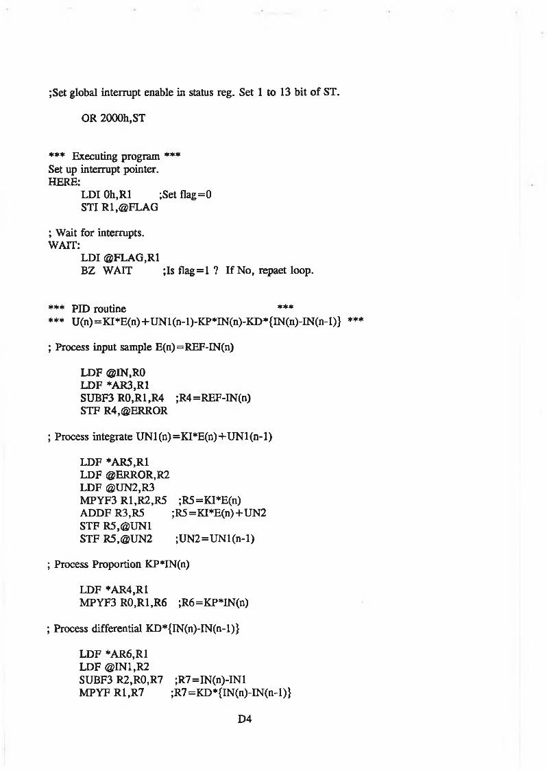
;Set global interrupt enable in status reg. Set 1 to 13 bit o f ST.
OR 2000h,ST
* * * Executing program ***Set up interrupt pointer.HERE:
LDI Oh.Rl ;Set flag=0STI R1,@FLAG
; Wait for interrupts.WAIT:
LDI @FLAG,R1BZ WAIT ;Is flag=l ? If No, repaet loop.
*** PID routine ****** U(n)=KI*E(n)+UNl(n-l)-KP*IN(n)-KD*{IN(n)-IN(n-l)} ***
; Process input sample E(n)=REF-IN(n)
LDF @IN,R0 LDF *AR3,R1SUBF3 R0,R1,R4 ;R4=REF-IN(n)STF R4,©ERROR
; Process integrate UNl(n)=KI*E(n)+UNl(n-l)
LDF *AR5,R1 LDF ©ERROR,R2 LDF @UN2,R3MPYF3 R1,R2,R5 ;R5=KI*E(n)ADDF R3,R5 ;R5=KI*E(n)+UN2STF R5,@UN1STF R5,@UN2 ;UN2=UNl(n-l)
; Process Proportion KP*IN(n)
LDF *AR4,R1MPYF3 R0,R1,R6 ;R6 =KP*IN(n)
; Process differential KD*{IN(n)-IN(n-l)}
LDF *AR6,R1 LDF @IN1,R2SUBF3 R2,R0,R7 ;R7=IN(n)-INl MPYF R1,R7 ;R7=KD*{IN(n)-IN(n-l)}
D4
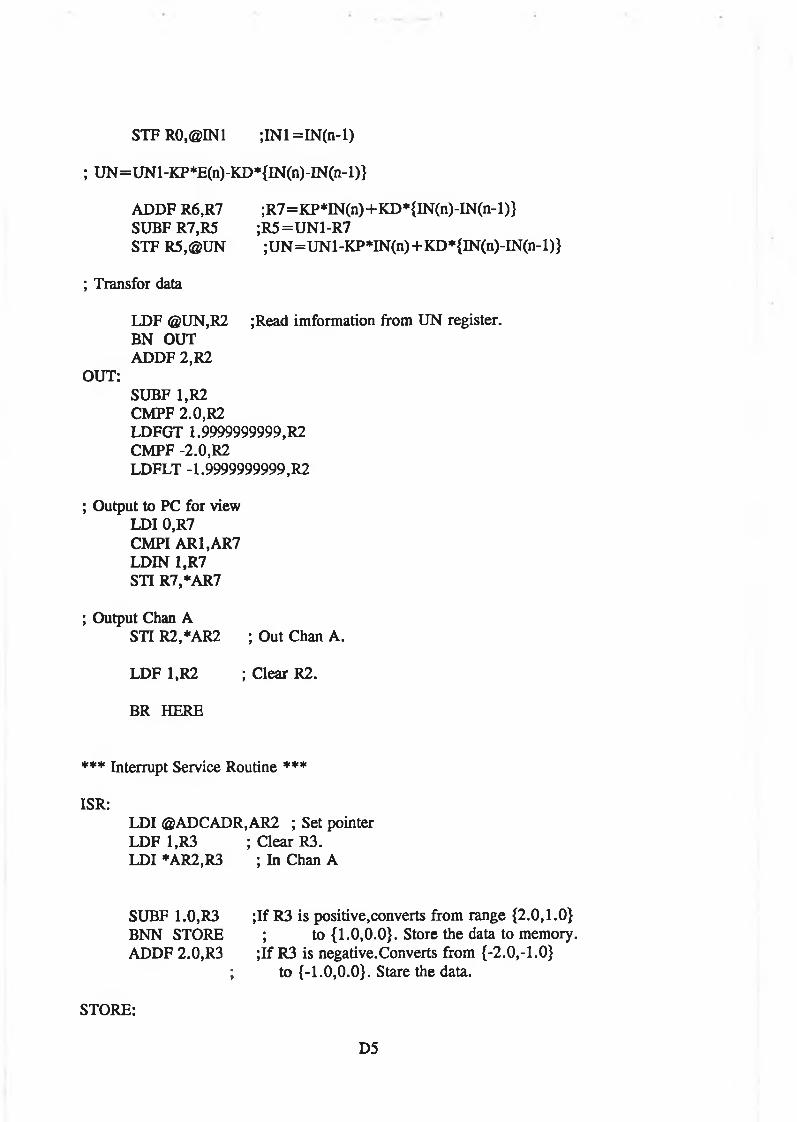
STF R0,@IN1 ;INl=IN(n-l)
; UN=UNl-KP*E(n)-KD*{IN(n)-IN(n-l)}
ADDF R6,R7 SUBF R7,R5 STF R5,@UN
;R7=KP*IN(n)+KD*{IN(n)-IN(n-l)};R5=UN1-R7;UN=UNl-KP*IN(n)+KD*{IN(n)-IN(n-l)}
; Transfor data
OUT:
LDF @UN,R2 ;Read imformation from UN register. BN OUT ADDF 2,R2
SUBF 1,R2 CMPF 2.0,R2 LDFGT 1.9999999999,R2 CMPF -2.0,R2 LDFLT -1.9999999999,R2
; Output to PC for view LDI 0,R7 CMPI AR1,AR7 LDIN 1,R7 STI R7,*AR7
; Output Chan ASTI R2,*AR2 ; Out Chan A.
LDF 1,R2 ; Clear R2.
BR HERE
*** Interrupt Service Routine ***
ISR:LDI @ADCADR,AR2 ; Set pointer LDF 1,R3 ; Clear R3.LDI *AR2,R3 ; In Chan A
SUBF 1.0,R3 ;If R3 is positive,converts from range {2.0,1.0}BNN STORE ; to {1.0,0.0}. Store the data to memory.ADDF 2.0,R3 ;If R3 is negative.Converts from {-2.0,-1.0}
; to {-1.0,0.0}. Stare the data.
STORE:
D5

STF R3,*AR1 + + STF R3,@IN
LDI 1,R0 STI RO,@FLAG
RETI
.end
; Set flag= l
D6
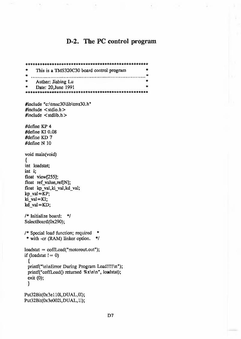
D-2. The PC control program
* * * * * * * * * * * * * * * * * * * * * * * * * * * * * * * * * * * * * * * * * * * * * * * * * * *
* This is a TMS320C30 board control program ** ** Auther: Jiabing Lu ** Date: 20,June 1991 ** sit*************************************************
¿include "c:\tmsc30\lib\tms30.h"¿include <stdio.h>¿include <stdlib.h>
¿define KP 4 ¿define KI 0.08 ¿define KD 7 ¿define N 10
void main(void){int loadstat; int i;float view[255];float ref_value,ref[N];float kp_val,ki_val,kd_val;kp_val=KP;ki_val—KI;kd_val=KD;
/* Initialize board: */SelectBoard(0x290);
/* Special load function; required ** with -cr (RAM) linker option. */
loadstat = coffLoad(Mmotorout.outH); if Ooadstat! = 0){printf("\n\nError During Program Load!!!!\n"); printf(McoffLoadO returned %x\n\n", loadstat); exit (0 );}
Put32Bit(0x3el 101,DUAL,01);Put32Bit(0x3e0021, DU AL, 11);
D7
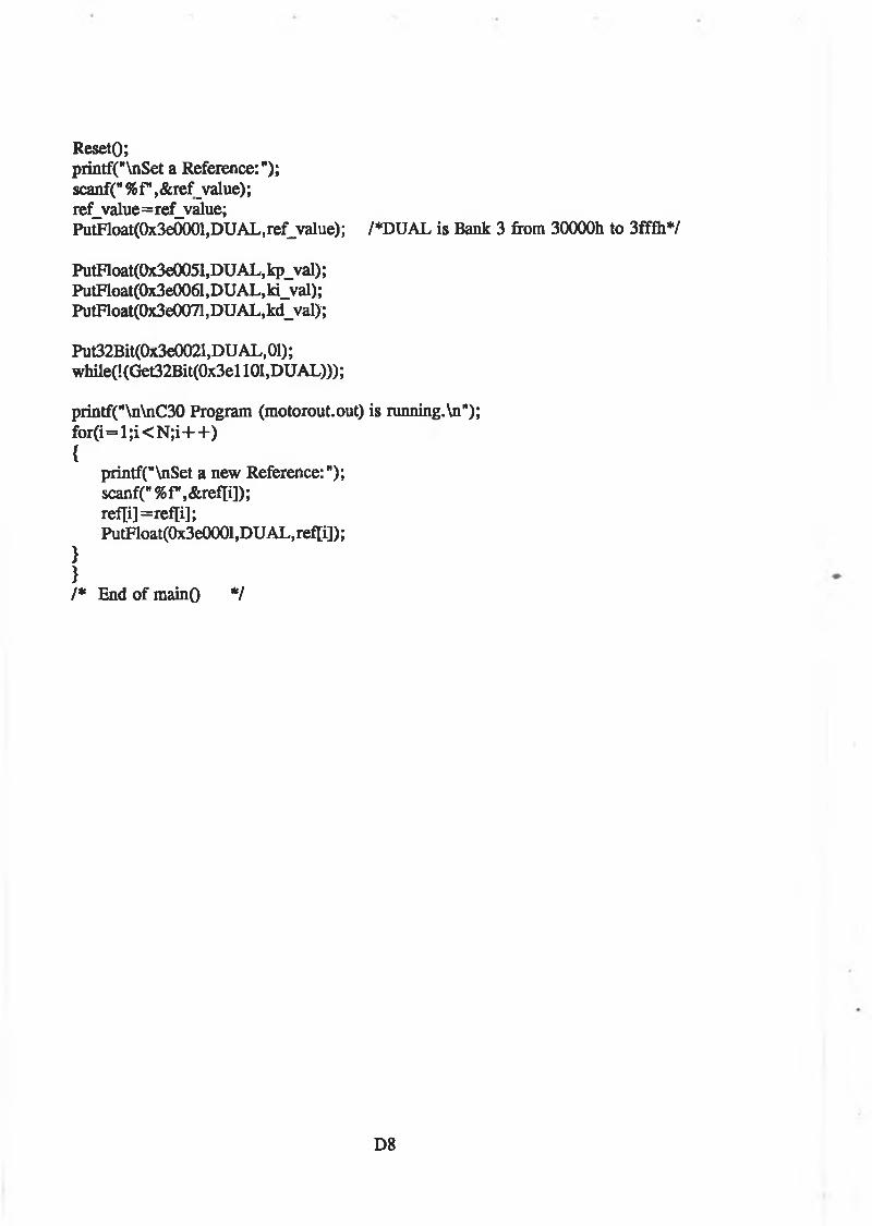
ResetO ;printf("\nSet a Reference:"); scanf(" %f\&ref_value); ref_value=ref_value;PutFloat(0x3e0001,DUAL, ref_value) ; /*DUAL is Bank 3 from 30000h to 3fffh*/
PutFloat(0x3e0051,DUAL,kp_val);PutFloat(0x3e0061,DUAL,ki_val) ;PutFloat(0x3e0071,DUAL,kd_val);
Put32Bit(0x3e0021,DUAL,01); while(!(Get32Bit(0x3el 101,DUAL)));
printf("\n\nC30 Program (motorout.out) is running.\n"); fo r (i= l; i< N ;i+ + ){
printf("\nSet a new Reference:"); scanf(" %r,&ref[i]); ref[i]=ref[i];PutFloat(0x3e0001,DUAL, ref[i]) ;
}}/* End of mainO */
D8
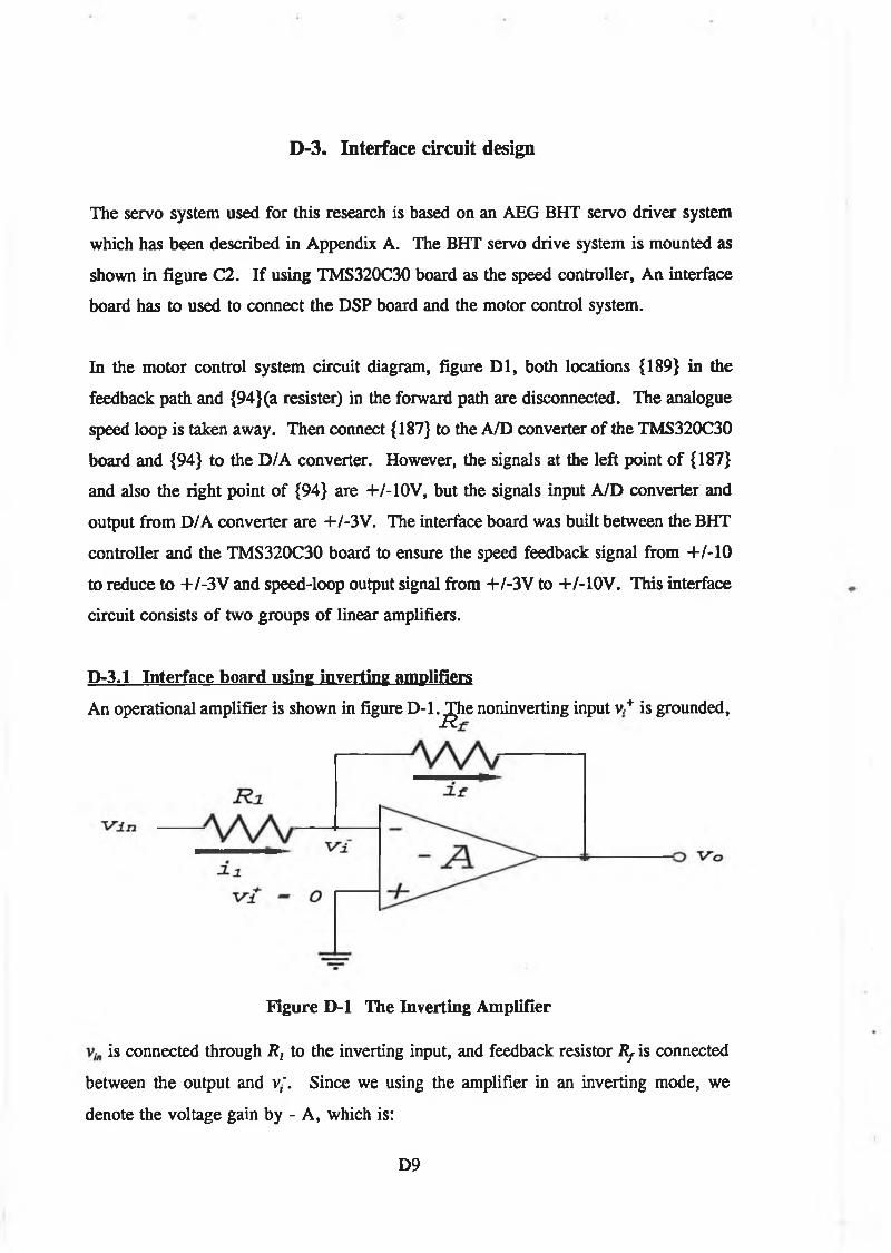
D-3. Interface circuit design
The servo system used for this research is based on an AEG BHT servo driver system
which has been described in Appendix A. The BHT servo drive system is mounted as
shown in figure C2. If using TMS320C30 board as the speed controller, An interface
board has to used to connect the DSP board and the motor control system.
In the motor control system circuit diagram, figure D l, both locations {189} in the
feedback path and {94}(a resister) in the forward path are disconnected. The analogue
speed loop is taken away. Then connect {187} to the A/D converter of the TMS320C30
board and {94} to the D/A converter. However, the signals at the left point of {187}
and also the right point of {94} are +/-10V, but the signals input A/D converter and
output from D/A converter are +/-3V. The interface board was built between the BHT
controller and the TMS320C30 board to ensure the speed feedback signal from +/-10
to reduce to + /-3V and speed-loop output signal from +/-3V to +/-10V. This interface
circuit consists of two groups of linear amplifiers.
D-3.1 Interface board using inverting amplifiersAn operational amplifier is shown in figure D-l.j£he noninverting input v * is grounded,
Figure D -l The Inverting Amplifier
is connected through R { to the inverting input, and feedback resistor Rf is connected
between the output and v,\ Since we using the amplifier in an inverting mode, we
denote the voltage gain by - A, which is:
D9
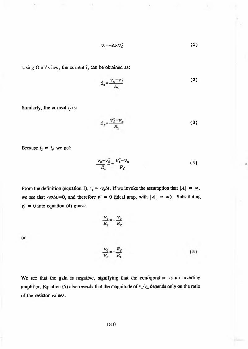
v0= -A x v i (1)
Using Ohm’s law, the current ij can be obtained as:
v€- v2 (2 )2l r T~
Similarly, the current if is:
(3)
Because i'; = ip we get:
ve-vi_ vi-v0 R, R*
(4)
From the definition (equation 1), v , '= - v J A . If we invoke the assumption that \A \ = oo,
we see that - v o /A = 0 , and therefore v, = 0 (ideal amp, with ¡/1| = oo). Substituting
v,' = 0 into equation (4) gives:
We see that the gain is negative, signifying that the configuration is an inverting
amplifier. Equation (5) also reveals that the magnitude of v j v ^ depends only on the ratio
of the resistor values.
DIO
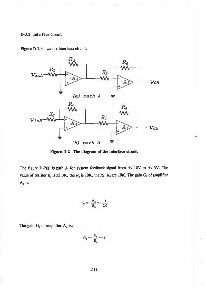
D-3.2 Interface circuit
Figure D-2 shows the interface circuit.
R iV in A —W v
r 5
VinB AAA"
( b ) p a t h B
Figure D-2 The diagram of the interface circuit
« VOA
c V O B
The figure D-2(a) is path A for system feedback signal from +/-10V to +/-3V. The
value of resister R j is 33.3K, the R 2 is 10K, the R3, R 4 are 10K. The gain G! of amplifier
At is:
The gain G2 of amplifier A2 is:
D ll
The gain GA of path A is:
G ,= — — =G,x<2,= - — x - l = — A i r 1 2 2 0 " > n
Ini 10
Figure D-2(b) is path B for speed-loop output signal from +/-3V to +/10V. The R s is
10K, the R 6 is 33.3K, the R 7, R? is also 10K. The gain G3 of amplifier A3 is
G,
The gain G4 of amplifier A4 is -1 same as A2. The gain G„ of path B is:
GB= ^ - = G 3xGi = - — x - 1 = — B Vim 3 3
The ID connecter (shown in figure C2) is used as the output connect of the BHT
controller. Because the analog speed-loop o f the BHT controller is not used, pins 5 and
5 of the ID connecter can be employed for the TMS320C30 controller. Pin 5 of ID is
used to connect {94}, and pin 5 of ID is used to connect {187}.
D12
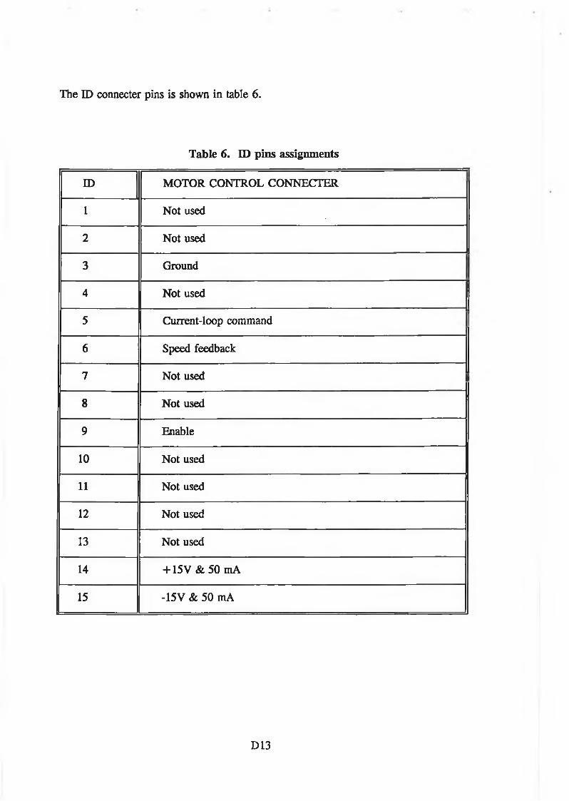
The ID connecter pins is shown in table 6.
Table 6. ID pins assignments
ID MOTOR CONTROL CONNECTER
1 Not used
2 Not used
3 Ground
4 Not used
5 Current-loop command !
6 Speed feedback
7 Not used
8 Not used
9 Enable
1 0 Not used
1 1 Not used
1 2 Not used
13 Not used
14 + 15V & 50 mA
15 -15V & 50 mA
D13
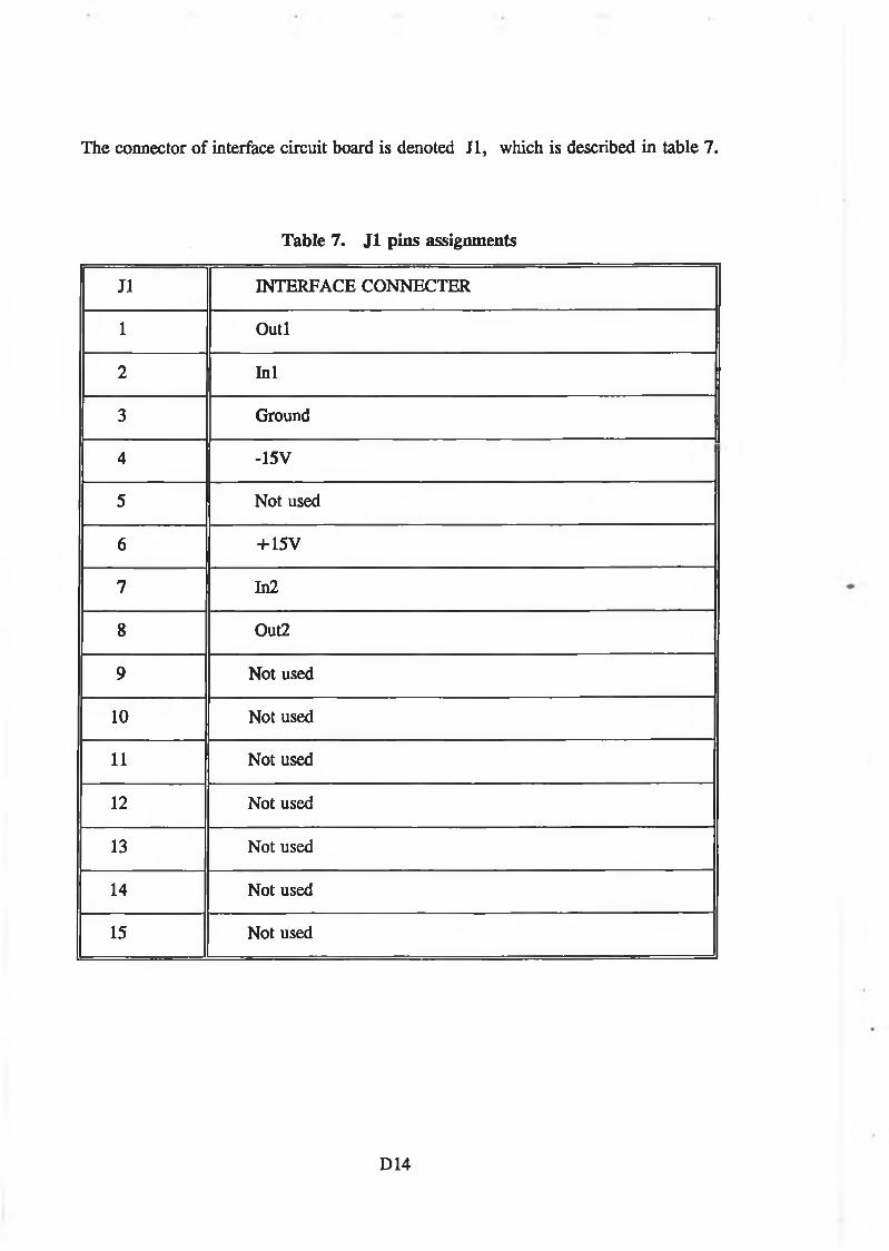
The connector of interface circuit board is denoted Jl, which is described in table 7.
Table 7. Jl pins assignments
Jl INTERFACE CONNECTER
1 Outl
2 Ini
3 Ground
4 -15V
5 Not used
6 + 15V
7 In2
8 Out2
9 Not used
1 0 Not used
1 1 Not used
1 2 Not used
13 Not used
14 Not used
15 Not used
D14
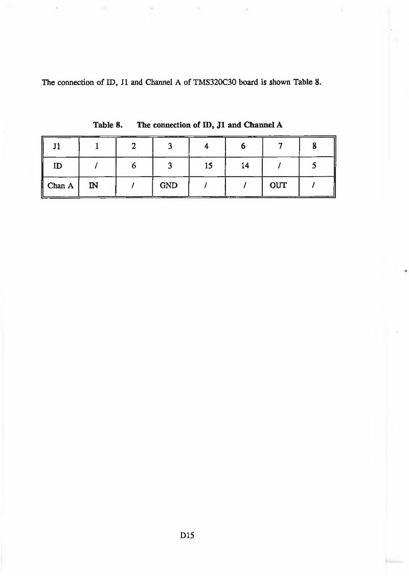
The connection of ID, J1 and Channel A of TMS320C30 board is shown Table 8.
Table 8. The connection of ID, J1 and Channel A
J1 1 2 3 4 6 7 8
ID / 6 3 15 14 / 5
Chan A IN / GND / / OUT /
D15