Embed Size (px)
Citation preview

Master Thesis IMIT/LECS/ [Year - 2005]
Design of a DS-UWB Transceiver
Master of Science Thesis In Electronic System Design
by
Saúl Rodríguez Dueñas
Stockholm, March 2005 Supervisor: Duo Xinzhong Examiner: Dr. Li-Rong Zheng

ii
i
ABSTRACT
Ultra Wide Band (UWB) is a new spectrum allocation which was recently
approved by the Federal Communication Commission (FCC) and is under study in Europe
and Asia. It has emerged as a solution to provide low complexity, low cost, low power
consumption, and high-data-rate wireless connectivity devices entering the personal space.
Any wireless system that has a fractional bandwidth greater than 20% and a total
bandwidth larger than 500MHz enters in the UWB definition. At the emission level, UWB
signals have a mask that limits its spectral power density to -41.3dBM/MHz between
3.1Ghz and 10.6GHz.
There are two approaches that have been studied in order to use the 7.5Ghz
allocated for UWB systems. First, OFDM techniques can be used to cover the entire
spectrum; these techniques are called multi-band UWB. On the other hand, the second
approach makes use of impulse radios which generate very-short-duration baseband pulses
that occupy the whole spectrum.
The objective of this thesis is to study, design, prototype, and test a UWB impulse
radio using off-chip components. A Direct Sequence (DS) UWB transceiver architecture
was selected. The transmitter uses first derivative Gaussian pulses that are modulated using
a bi-phase modulation technique. The pulse rate of the system is 100MHz and the bit rates
under investigation were 100Mbps, 50Mbps, 25Mbps, and 10Mbps. The transmitter and
receiver were divided in functional blocks in order to execute system level simulations.
The transmitter was implemented in both schematics and layout, and the UWB pulse
generator block was constructed and tested in order to validate its functionality. On the
other hand, the off-chip implementation of the receiver presented particular difficulties that
made its construction not possible in this study. As a result, the blocks of the receiver were
implemented in Matlab and the performance of the whole transceiver was estimated
through numeric simulations. Finally, a case study for the multi-user capability of the
system was presented.

ii
iii
ACKNOWLEDGEMENTS
I would like to thank my friends and colleges for supporting and encouraging me
during my studies in KTH. In particular, I would like to thank Dr. Li-Rong Zheng for
giving me the opportunity to conduct Ultra Wide Band research. I would like to express my
gratitude to my supervisor, Duo Xinzhong, for his guidance and patience along this project.
His advice and help were absolutely invaluable. I wish to express my great appreciation to
Ling Yang Zhang for her friendly suggestions that helped a lot to improve this manuscript.
Finally, I reserve the most special gratitude for my family in Ecuador. Without your
unconditional support and love, this could have been impossible. I will never be able to
repay all the sacrifices and hardships that you had to endure. I hope my humble
accomplishments can compensate at least in part all the things you have done for me.

iv
v
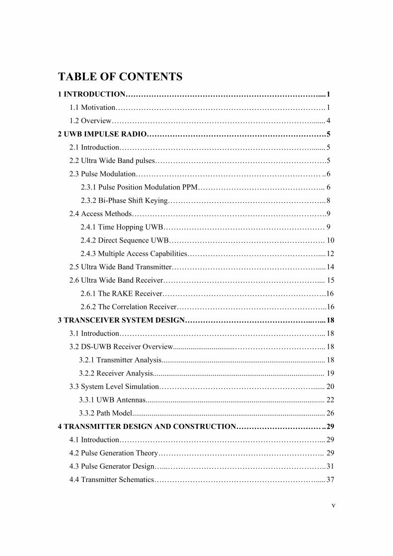
TABLE OF CONTENTS 1 INTRODUCTION………………………………………………………………….... 1
1.1 Motivation………………………………………………………………………. 1
1.2 Overview……………………………………………………………………....... 4
2 UWB IMPULSE RADIO……………………………………………………………. 5
2.1 Introduction…………………………………………………………………....... 5
2.2 Ultra Wide Band pulses…………………………………………………………. 5
2.3 Pulse Modulation……………………………………………………………… .. 6
2.3.1 Pulse Position Modulation PPM………………………………………….. 6
2.3.2 Bi-Phase Shift Keying…………………………………………………….. 8
2.4 Access Methods…………………………………………………………………. 9
2.4.1 Time Hopping UWB……………………………………………………… 9
2.4.2 Direct Sequence UWB……………………………………………………. 10
2.4.3 Multiple Access Capabilities…………………………………………….... 12
2.5 Ultra Wide Band Transmitter………………………………………………….... 14
2.6 Ultra Wide Band Receiver…………………………………………………….... 15
2.6.1 The RAKE Receiver……………………………………………………….16
2.6.2 The Correlation Receiver…………………………………………………..16
3 TRANSCEIVER SYSTEM DESIGN…………………………………………..…... 18
3.1 Introduction……………………………………………………………………... 18
3.2 DS-UWB Receiver Overview................................……………………………... 18
3.2.1 Transmitter Analysis..................................................................................... 18
3.2.2 Receiver Analysis......................................................................................... 19
3.3 System Level Simulation……………………………………………………...... 20
3.3.1 UWB Antennas............................................................................................. 22
3.3.2 Path Model.................................................................................................... 26
4 TRANSMITTER DESIGN AND CONSTRUCTION…………………………… .. 29
4.1 Introduction……………………………………………………………………... 29
4.2 Pulse Generation Theory……………………………………………………….. 29
4.3 Pulse Generator Design…...…………………………………………………….. 31
4.4 Transmitter Schematics………………………………………………………..... 37

vi
4.5 Transmitter Layout…………....……………………………………………….. .. 39
4.6 Momentum Simulation........….…………………………………………………. 41
4.7 Assemblage of the test structures.......................................................................... 43
5 RECEIVER DESIGN.................……………………………………………………. 45
5.1 Introduction……………………………………………………………………... 45
5.2 Receiver RF Front-End……..…………………………………………………... 45
5.3 Noise Analysis and LNA Requirement ...………………………………………. 45
5.4 Correlator……………………………………………………………………….. 50
5.5 Jitter Analysis………………………………………………………………….. .. 53
6 SYSTEM SIMULATION AND TEST RESULTS..........................................…….. 54
6.1 Introduction…………………………………………………………………….. 54
6.2 System Level Simulation……………………………………………………..... 54
6.3 Pulse generator Test……………………………………………………………. 59
6.4 Case Study……………………………………………………………………… 63
7 CONCLUSIONS…………………………………………………………………… .. 65
8 FUTURE WORK……………………………………………………………………. 67
9 LIST OF SYMBOLS AND ABBREVIATIONS…………………………………. .. 68
10 REFERENCES……………………………………………………………………... 70
APPENDIX A TRANSMITTER SCHEMATICS…………………………………… 72
1
1 INTRODUCTION 1.1 Motivation
Opposite to what many people may think, Ultra Wide Band (UWB) signals are not
a new concept in wireless communications. Research on impulse radar technology was
done during 1940s and 1960s, and the first patents for short-pulse receivers were granted
then. Originally, this concept was called carrierless or impulse technology due to its nature.
The term UWB started to be used in the 1980s when it surged a new interest in research for
potential applications.
UWB signals are defined as signals that have a fractional bandwidth greater than
20% of the center frequency measured at -10dB points and occupy at least 500MHz. Here,
fractional bandwidth is defined as 2(FH - FL)/(FH + FL) and the center frequency (FH + FL)/2.
The theoretical motivation why UWB is so attractive can be better explained using the
Shannon theorem which relates the capacity of a system with its bandwidth and signal to
noise ratio. It is expressed as:
+=
02 1log
BNPBC (1.1)
Where:
C is the channel capacity (bps)
B is the channel bandwidth (Hz)
P is the signal power (W)
No is the noise power spectral density (W/Hz)
From the previous equation it is clear that the capacity of a communication system
increases faster as function of the channel bandwidth than as function of the power.
However, traditional wireless systems have evolved using narrowband systems that are
power limited and therefore have a limited channel capacity. On the other hand, the
increasing need of high data rates in wireless communication applications will require the
use of wide band systems capable of handling several GHz in order to accomplish the
demands. Therefore, UWB technology has emerged as a solution for high data rates
2
systems.
The UWB systems show properties that make them attractive for many applications.
For example, they are inherently resistant to multi-path fading due to the fact that it is
possible to resolve differential delays between pulses on the order of 1ns. Furthermore, as
the signals are spread in a wide bandwidth, they show a low power spectral density which
makes them suitable for Low Probability of Detection (LPD) systems. Applications that
have been envisioned for these systems are for example: low complexity, low cost,
low-power consumption, and high data rates wireless connectivity of devices entering the
personal space, range finding and self-location systems, and terrain mapping radars.
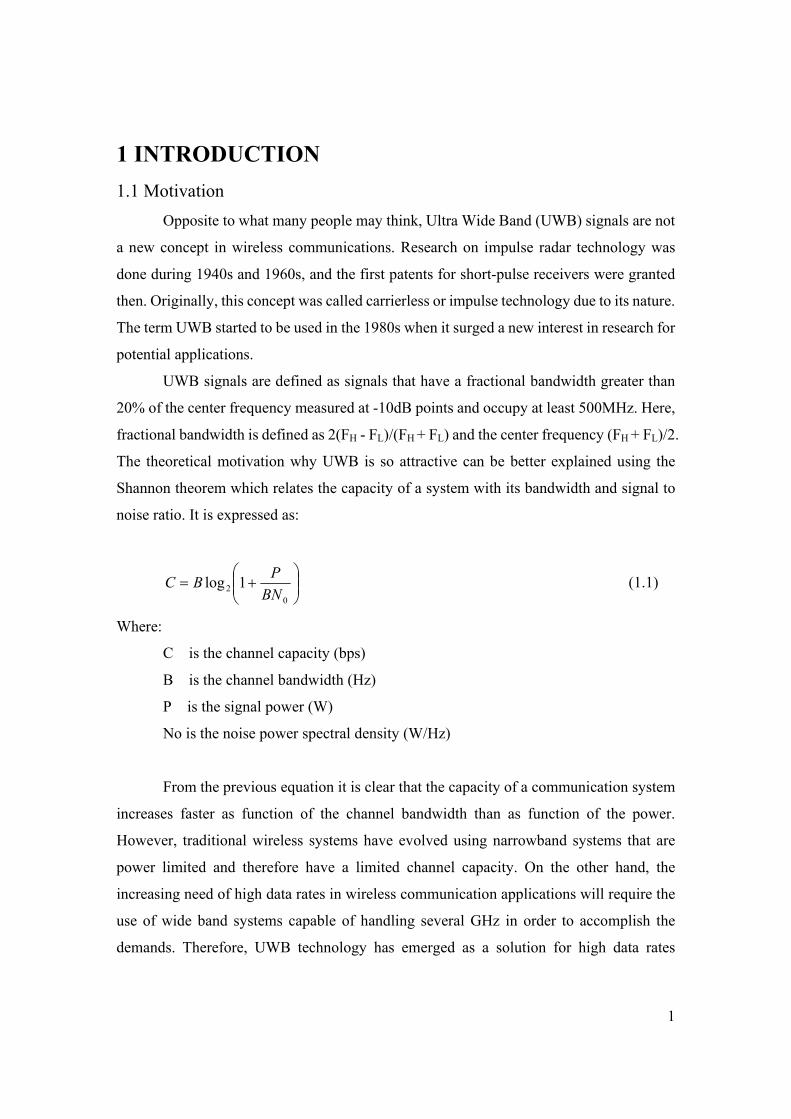
In order to regulate the use of UWB systems, the FCC has allocated frequency
spectrum from 3.1GHz to 10.6GHz, and the average output power has been limited to
-41.3dBm/MHz. Figure 1.1 shows how the FCC has set the UWB mask.
Figure 1.1 UWB Mask as described by the FCC
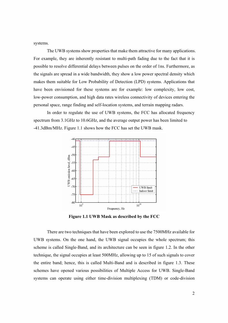
There are two techniques that have been explored to use the 7500MHz available for
UWB systems. On the one hand, the UWB signal occupies the whole spectrum; this
scheme is called Single-Band, and its architecture can be seen in figure 1.2. In the other
technique, the signal occupies at least 500MHz, allowing up to 15 of such signals to cover
the entire band; hence, this is called Multi-Band and is described in figure 1.3. These
schemes have opened various possibilities of Multiple Access for UWB. Single-Band
systems can operate using either time-division multiplexing (TDM) or code-division
3
multiplexing (CDM), whereas Multi-Band systems can also make use of frequency
division multiplexing (FDM) techniques.
Figure 1.2 Possible architecture for an impulse radio
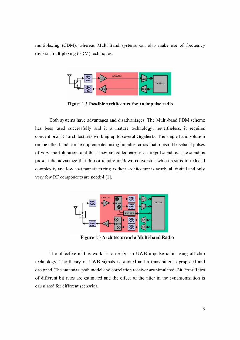
Both systems have advantages and disadvantages. The Multi-band FDM scheme
has been used successfully and is a mature technology, nevertheless, it requires
conventional RF architectures working up to several Gigahertz. The single band solution
on the other hand can be implemented using impulse radios that transmit baseband pulses
of very short duration, and thus, they are called carrierless impulse radios. These radios
present the advantage that do not require up/down conversion which results in reduced
complexity and low cost manufacturing as their architecture is nearly all digital and only
very few RF components are needed [1].
Figure 1.3 Architecture of a Multi-band Radio
The objective of this work is to design an UWB impulse radio using off-chip
technology. The theory of UWB signals is studied and a transmitter is proposed and
designed. The antennas, path model and correlation receiver are simulated. Bit Error Rates
of different bit rates are estimated and the effect of the jitter in the synchronization is
calculated for different scenarios.

4
1.2 Overview This thesis has been divided in 7 chapters. Chapter 2 presents an analysis of UWB
systems. Pulse generation, modulation, and detection techniques are discussed. Multiple
access schemes are also presented. Chapter 3 deals with the transceiver architecture design
based on the selection of a pulse waveform, modulation scheme, and multiple access
technique. The blocks of the transceiver are defined and a system level simulation using
ADS and Matlab is proposed. Chapter 4 explains the design and construction of the
transmitter. The pulse generation is discussed and each block of the transmitter is
translated to circuit schematics. A netlist is extracted from the schematic and a PCB Layout
is generated. Special attention is taken with the microstrips lines. Critical RF paths are
extracted and simulated in ADS using momentum simulation. Chapter 5 provides a study
of the design of the receiver. The correlation receiver is selected and its blocks are defined.
Chapter 6 presents the verification of the design. The system simulation proposed in
chapter 3 is executed, and its results are presented. In addition, the hardware of the pulse
generators is tested. Chapter 7 contains the conclusions of the thesis and the results are
discussed in detail. The thesis concludes with some suggestions for future work in Chapter
8.
5
2 UWB IMPULSE RADIO 2.1 Introduction
Ultra Wide Band impulse radios are microwave systems that communicate using
baseband pulses of very short duration. Pulse Generation, modulation, and multiple access
are time domain dependent functions. Therefore, instead of characterizing these systems in
the frequency domain as most wireless systems, their behavior is better defined in the time
domain. These systems are described using their impulse response. Hence, they are known
as impulse radios.
In order to understand the impulse response, it is important to note that the output of
a system in the time domain is defined with the convolution formula:
∫∞
∞−
−= duutxuhty )()()( 2.1
Where x(t) is the input of the system and y(t) is its output. When x(t) is equal to a
Dirac pulse, the output is equal to h(t) which is defined as the impulse response of the
system.
2.2 Ultra Wide Band Pulses
The baseband pulses used by UWB signals have very short time duration in the
range of a few hundred picoseconds. These signals have frequency response from nearly
zero hertz to a few GHz. As there is no standardization yet, the shape of the signal is not
restricted, but its characteristics are restricted by the FCC mask.
A good candidate shape for the UWB signal is the first derivative of a Gaussian
pulse, which is mathematically defined as: 2
)(
−
= τ
τ
t
ettV 2.2
The waveform and spectrum of this pulse is showed in fig 2.1. Both the center
frequency and the bandwidth of the signal are determined by τ, that in this case it is equal to
6
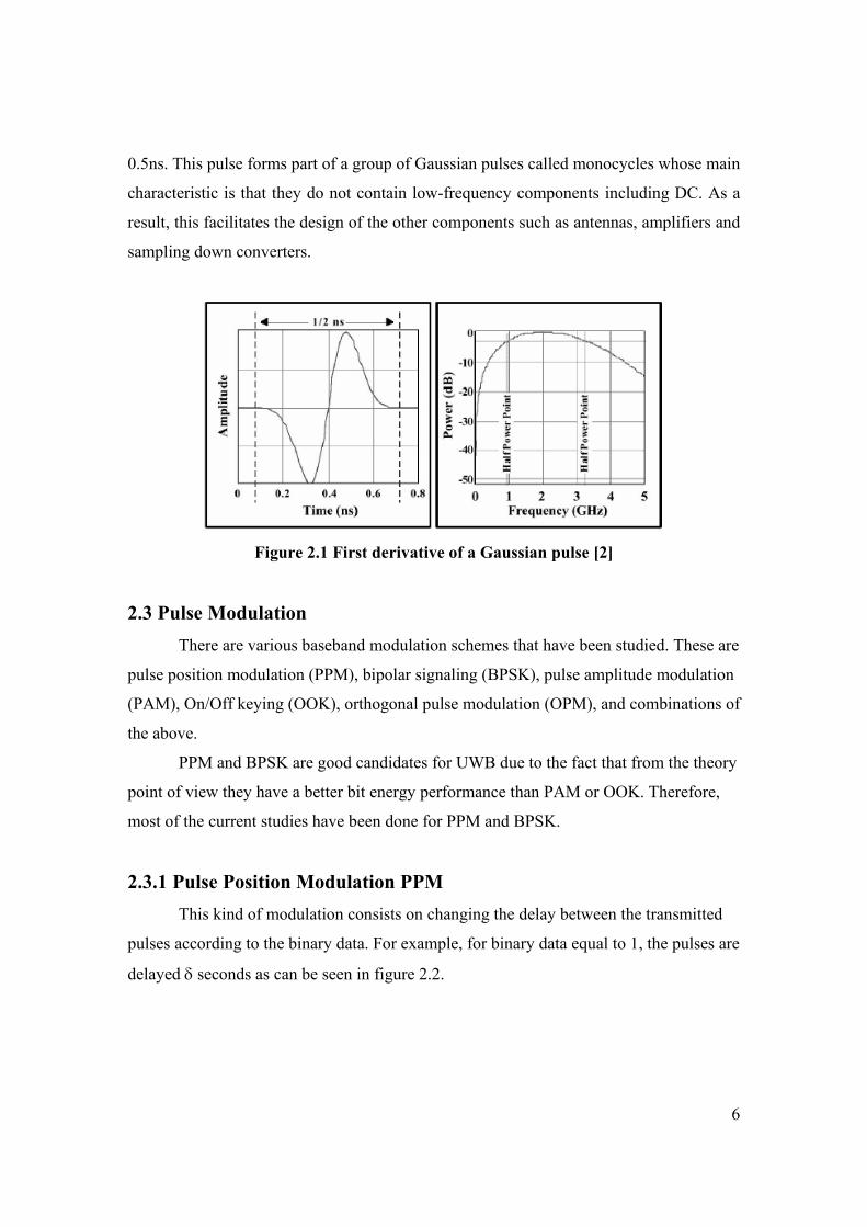
0.5ns. This pulse forms part of a group of Gaussian pulses called monocycles whose main
characteristic is that they do not contain low-frequency components including DC. As a
result, this facilitates the design of the other components such as antennas, amplifiers and
sampling down converters.
Figure 2.1 First derivative of a Gaussian pulse [2]
2.3 Pulse Modulation
There are various baseband modulation schemes that have been studied. These are
pulse position modulation (PPM), bipolar signaling (BPSK), pulse amplitude modulation
(PAM), On/Off keying (OOK), orthogonal pulse modulation (OPM), and combinations of
the above.
PPM and BPSK are good candidates for UWB due to the fact that from the theory
point of view they have a better bit energy performance than PAM or OOK. Therefore,
most of the current studies have been done for PPM and BPSK.
2.3.1 Pulse Position Modulation PPM
This kind of modulation consists on changing the delay between the transmitted
pulses according to the binary data. For example, for binary data equal to 1, the pulses are
delayed δ seconds as can be seen in figure 2.2.

7
Figure 2.2 PPM Waveform
Mathematically, the modulated data can be expressed as:
∑ ∞=
−∞=×−−=
j
jdjjTtwty )()( δ
2.3
Where:
W is the pulse waveform
T is the bit time
δ is a fixed delay
dj is the binary data
The Bit Error Rate (BER) vs. Eb/No curve of PPM can be seen in figure 2.3.
Figure 2.3 BER vs. Eb/No curve of PPM Modulation

8
2.3.2 Bi-Phase Shift Keying This modulation is also called antipodal and consists in changing the polarity of the
transmitted pulses according to the incoming data as can be shown in the figure 2.4.
Figure 2.4 Bi-Phase Shift Keying Waveform
The bi-phase modulation can be expressed as:
∑ ∞=
−∞=−−=
j
jdjjTtwty )12)(()(
2.4
Where:
w is the pulse waveform
T is the bit time
dj is the binary data
The BER vs. Eb/No curve for BPSK can be seen in figure 2.5.
Figure 2.5 BER vs Eb/No of Bi-Phase Modulation

9
2.4 Access Methods There are two spread-spectrum multiple-access techniques that have been
considered to be used with UWB impulse radios: direct sequence (DS-UWB) and time
hopping (TH-UWB). Both techniques use pseudo-noise codes to separate different users.
2.4.1 Time Hopping UWB In TH-UWB, the transmitted signal for one user using antipodal bi-phase signal is
defined as:
)12()( / −−−= ∑ ∞=
−∞= Nsjj
j jftrtr dTccjTtws 2.5
Where:
w is the pulse waveform
Tf is the pulse repetition time
cj is a pseudorandom code different for each user
Tc is a slot time
d is the binary data
Ns is an integer which indicates the number of pulses transmitted for each bit
An example of the antipodal modulation using TH multiple access technique can be
seen in figure 2.6.
Figure 2.6 Example of TH-UWB with Bi-Phase Modulation
And the TH-UWB signal using PPM can be defined as:
10
∑ ∞=
−∞=−−−=
j
j Najjftrtr dTccjTtws )( /δ 2.6
Where:
w is the pulse waveform
Tf is the pulse repetition time
cj is a pseudorandom code different for each user
δ is a fixed delay
d is the binary data
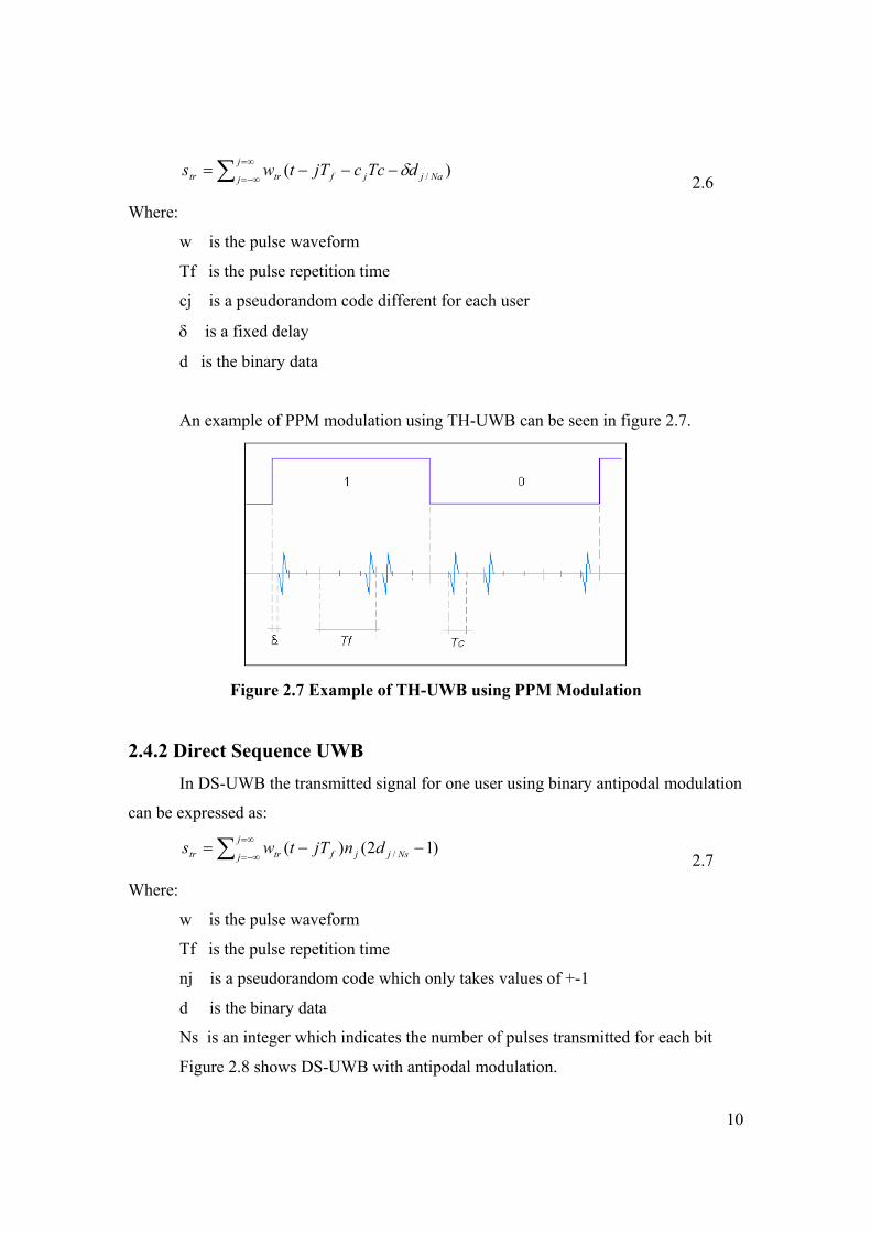
An example of PPM modulation using TH-UWB can be seen in figure 2.7.
Figure 2.7 Example of TH-UWB using PPM Modulation
2.4.2 Direct Sequence UWB In DS-UWB the transmitted signal for one user using binary antipodal modulation
can be expressed as:
)12()( / −−= ∑ ∞=
−∞= Nsjj
j jftrtr dnjTtws 2.7
Where:
w is the pulse waveform
Tf is the pulse repetition time
nj is a pseudorandom code which only takes values of +-1
d is the binary data
Ns is an integer which indicates the number of pulses transmitted for each bit
Figure 2.8 shows DS-UWB with antipodal modulation.
11
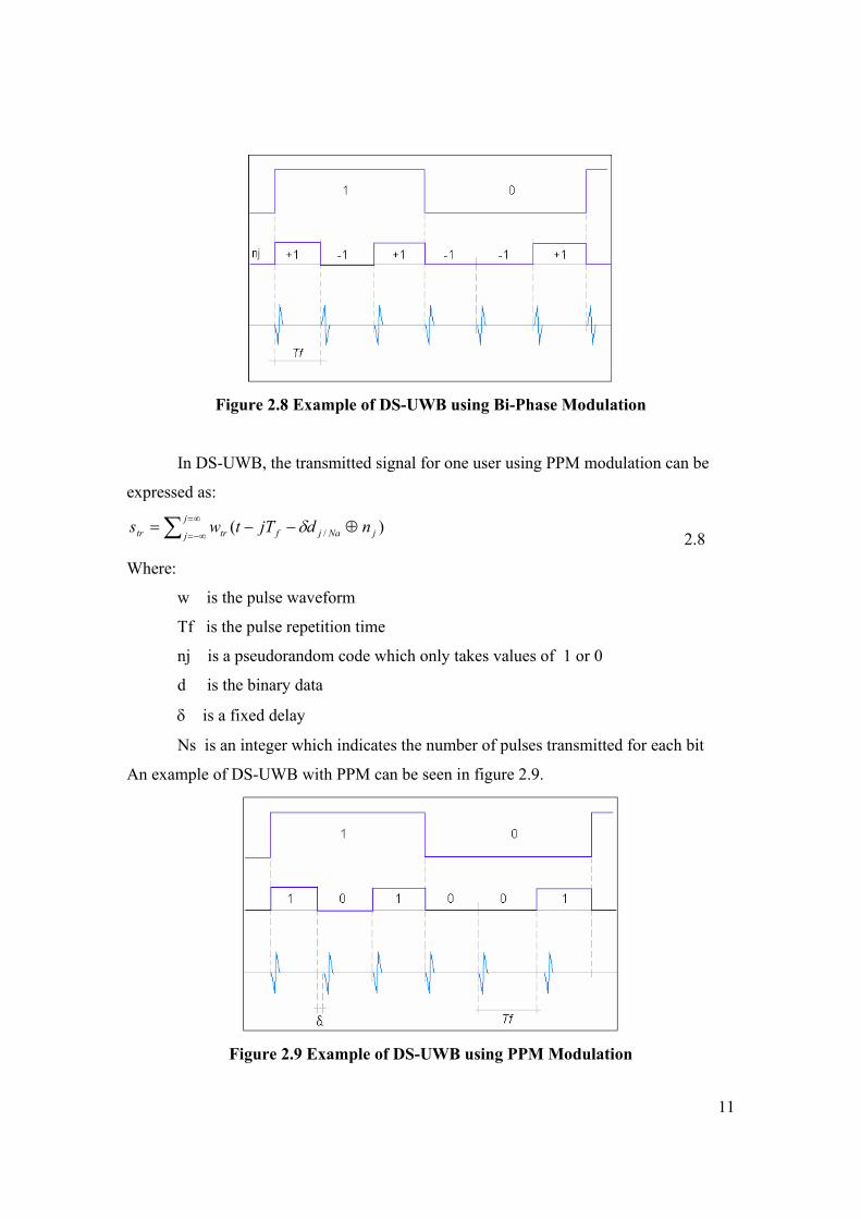
Figure 2.8 Example of DS-UWB using Bi-Phase Modulation
In DS-UWB, the transmitted signal for one user using PPM modulation can be
expressed as:
∑ ∞=
−∞=⊕−−=
j
j jNajftrtr ndjTtws )( /δ 2.8
Where:
w is the pulse waveform
Tf is the pulse repetition time
nj is a pseudorandom code which only takes values of 1 or 0
d is the binary data
δ is a fixed delay
Ns is an integer which indicates the number of pulses transmitted for each bit
An example of DS-UWB with PPM can be seen in figure 2.9.
Figure 2.9 Example of DS-UWB using PPM Modulation

12
2.4.3 Multiple Access Capability
As any multiple access system, the overall performance of UWB impulse radios is
degraded when the number of users who are sharing the channel is increased. In order to
satisfy the performance specification of bit error rate (BER), the signal to noise radio in the
receiver must be controlled. Moreover, there is a limit in the number of users that can share
a channel. This situation has been studied for TH-UWB and it has been found that the
number of users is a function of the fractional increase in required power in order to
maintain a fixed BER, and is expressed as [17]:
1)101()( 10/11 +−=∆ ∆−−− PspecSNRMPNu 2.9
Where:
Nu is the number of users
M is the modulation coefficient
SNR is the signal to noise radio of the specifications
∆P is the increase in required power to maintain a constant BER
The following example in figure 2.10 illustrates how the number of users can
increase with an increase of the additional power for a UWB link with M = 2.63 x 10⁵ and
bit rate of 19.2 kbps.
Figure 2.10 Example of number of users vs. additional required power TH-UWB[1]

13
It is clear that the function is monotonically increasing, and there is an upper limit
to the number of users that can use the channel maintaining the same BER. The maximum
number of users in a TH-UWB system can be calculated:
1)(lim 11max +=∆= −−
∞→∆SNRMPNuN
P 2.10
On the other hand, the number of users that can share a DS-UWB channel can be
calculated using the equations derived for DS-CDMA in previous literature [16].
In general, the important parameter to establish the performance of a receiver in a
digital communication system operating in an AWGN channel is the ratio between the bit
energy and the power spectral density of the noise, Eb/No. Depending on different
modulation techniques and channel coding, it is possible to obtain curves of BER vs.
Eb/No. However, the parameter that the radio designer commonly uses during the design
and implementation of the system is the SNR. Hence, it is important to obtain the
relationship between them. This relationship can be derived as:
BPTbPs
NoEb
N /×
= 2.11
Where
Eb is the average energy of a bit (J)
No is the noise power spectral density (W/Hz)
Ps is the average power of the signal (W)
Tb is the duration of one bit (s)
PN is the power of the noise (W)
B is the bandwidth of the signal (Hz)
However, Ps/PN is equivalent to the SNR. Also, Tb is equal to 1/r, where r is the bit
rate (bps). Hence equation 2.11 can be expressed as:
rBSNR
NoEb
×= 2.12
In this equation the bit energy is referred to No which is thermal noise that is

14
described as a white noise process with a Gaussian distribution. This situation permits to
extend equation 2.12 to the case of multiple users sharing the channel. Indeed, from the
statistic point of view, the addition of users using different orthogonal pseudo noise codes
appears as an increase in the noise level during the detection process, and hence, it has
additive characteristics that are Gaussian in nature. Consequently, No can be renamed Io,
which is the power spectral density of the thermal noise and the intererence produced by
other users. Then, equation 2.12 can be expressed for the multi-user environment as:
( )dB
dBdB r
BSNRIoEb
+=
2.13
Where the term B/r is also called processing gain. The relationship that allows to
obtaining the maximum number of users can be found by expanding the SNR. For
simplicity, it is assumed that all the signals arrive with the same power and also that the
addition of multiple interferers dominates the power of the noise. Then, this relationship
can be expressed as:
11
)1( −=
−==
uuN NPsNPs
PPsSNR 2.14
In conclusion, the maximum number of users is inversely proportional to the SNR.
Here it was assumed that the pseudo noise codes are orthogonal, and that there is some kind
of power control in the system. In practice, this is difficult to achieve and as a result the
SNR required to maintaining a target BER is larger than that described in 2.13. Finally it is
important to note that as in any communication system, the information can be coded using
block or convolutional Forward-Error-Correction (FEC) codes in order to improve the gain
at expenses of reducing the bit rate.
2.5 UWB Transmitter The functional structure of the transmitter for TH-UWB and DS-UWB can be
described using figure 2.11.

15
Figure 2.11 UWB Transmitter
When the modulation is PPM, the blocks of modulation and code generation
control a programmable time delay. If the modulation is Bi-Phase, the block of modulation
controls the pulse generator. The programmable-time delay determines the time when the
pulse generator will be triggered. In the case of TH-UWB, this block causes the
time-hopping of the signal that permits the multiple access. Besides, it is used as data
modulator when the scheme is PPM. In the DS-UWB, the programmable delay is only used
if the signal has a PPM modulation scheme. In case of DS-UWB with Bi-Phase modulation,
the programmable time delay is omitted, and the block of modulation and code generation
control directly the pulse generator.
From the above descriptions it is possible to conclude that no carrier modulation is
required in any stage which results in a simplified architecture. Also, as the required power
level is very low, power amplifiers are not needed. Finally, the antennas behave as filters,
and therefore their effect must be considered.
2.6 UWB Receiver
The detection of extremely short pulses requires highly specialized receivers. Due
to the characteristics of the impulse radios, up/down conversion is not required. The most
common UWB receivers found in the current literature are the RAKE receiver and the
correlation receiver.
16
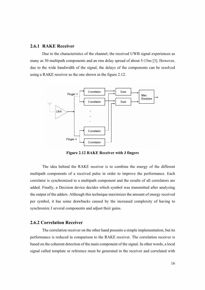
2.6.1 RAKE Receiver Due to the characteristics of the channel, the received UWB signal experiences as
many as 30 multipath components and an rms delay spread of about 5-15ns [3]. However,
due to the wide bandwidth of the signal, the delays of the components can be resolved
using a RAKE receiver as the one shown in the figure 2.12.
Figure 2.12 RAKE Receiver with J fingers
The idea behind the RAKE receiver is to combine the energy of the different
multipath components of a received pulse in order to improve the performance. Each
correlator is synchronized to a multipath component and the results of all correlators are
added. Finally, a Decision device decides which symbol was transmitted after analyzing
the output of the adders. Although this technique maximizes the amount of energy received
per symbol, it has some drawbacks caused by the increased complexity of having to
synchronize J several components and adjust their gains.
2.6.2 Correlation Receiver The correlation receiver on the other hand presents a simple implementation, but its
performance is reduced in comparison to the RAKE receiver. The correlation receiver is
based on the coherent detection of the main component of the signal. In other words, a local
signal called template or reference must be generated in the receiver and correlated with

17
the received signal. The structure of the correlation receiver is shown in figure 2.13:
Figure 2.13 Correlation Receiver
As can be seen, the correlator is formed by a mixer and an integrator. The output of the
integrator is fed to a decision device, for example a comparator which decides whether a
one or zero was transmitted.
Ideally, the local signal should be the same signal that was transmitted. However,
due to the fact that the medium is not perfect, the received pulses are modified versions of
the transmitted ones. This situation is particularly problematic in UWB and the
performance of the system is highly dependent on an accurate selection of the local
reference signal.

18
3 ARCHITECTURE OF A DS-UWB TRANSCEIVER 3.1 Introduction
After studying the options of modulation and access methods that were presented in
the previous chapter, it was decided to design the UWB transceiver using Bi-Phase
modulation and Direct Sequence multiple access. This scheme presents theoretical and
practical advantages for this project. First, the synchronization in TH-UWB is more
difficult to achieve than in DS-UWB [3]. This situation can be worsened if PPM is used
since timing precision in the order of a few picoseconds is needed to maintain an
acceptable performance. Furthermore, the implementation of the programmable time delay
with these requirements brings a lot of complexity for an off-chip solution. On the other
hand, the BER vs. Eb/No curves show that bi-phase modulation has a better performance
than PPM. Also, bi-phase modulation has an easier implementation.
This chapter explains the architecture of the whole DS-UWB transceiver. The
transmitter and receiver are analyzed and the feasibility of their implementation is
discussed. It was found that it is possible to build the blocks of the transmitter off-chip. The
receiver, on the other hand, presents many difficulties that make its off-chip
implementation not possible. However, a system level simulation is proposed in order to
evaluate the performance of the transceiver.
3.2 DS-UWB Transceiver Overview
3.2.1 Transmitter Analysis The structure of the proposed transmitter can be seen in figure 3.1. An oscillator
controls two monocycle generators. One of the generators produces positive pulses
whereas the other produces negative pulses. The modulation is done using a switch which
is controlled digitally by the data modulation block. The data modulation block is a digital
part that processes the information that will be transmitted. Here, the data are processed at
a specific bit rate and direct sequence coding is done. This solution gives a lot of flexibility
because the digital data that control the RF switch can be generated and modified
externally.

19
Figure 3.1 Structure of the Transmitter
The block of the oscillator can be implemented using a commercial oscillator with
fast rise and fall times (close to 1ns), and with low jitter. Since the highest bitrate of the
system is 100Mbps, the required oscillator should have at least 100MHz. The pulses
generated at this frequency have a period of 10ns, which is fairly enough to receive the
monocycles without considerable interference due to multi-path [6].
There are different solutions for the implementation of the pulse generators. It is
possible to build, for instance, CMOS analog circuits that create the monocycle waveform,
MOSFET switched capacitors, and shorted transmission lines with self recovering diodes.
However, since the idea was to prototype the transmitter using available components,
on-chip solutions were excluded.
The solution using shorted transmission lines and self recovering diodes was
interesting for this project as the copper traces on Printed Circuit Board (PCB) can be
designed as microstrip lines [4]. Finally, the switch required to achieve the data modulation
is a device that must work within the UWB band. Currently, it is possible to buy
commercial RF switches that work in the lower part of the UWB band. Nonetheless, the
switching speed of these devices places a limit in the maximum pulse rate of the system.
3.2.2 Receiver Analysis The receiver of the UWB transceiver was designed using the correlator receiver
architecture described in chapter 2. This circuit implementation presents many challenges
20
for an off-chip solution. The LNA, Mixer, integrator, and a programmable delay must be
selected from commercial components or designed separately. Currently, it is possible to
find RF amplifiers that can be used as LNAs for UWB systems. For instance, the
Minicircuits’ ERA family of amplifiers achieves gains of almost 10 dB with bandwidths
that ranges from DC - 8GHz and noise figures of 4dB. Likewise, commercial
state-of-the-art mixers such as the Minicircuits’ LMA broad band series have a range from
500 to 5000MHz and a conversion loss of approximately 8dB.
The integrator, on the other hand, requires a reset signal every bit time, and needs to
have a very broad band response; hence, it has to be designed. Furthermore, the fact that
the baseband processing controls the synchronization process places a strong limitation.
Finally, the programmable time-delay, is perhaps the most complex part of the receiver. It
must achieve phase delays with steps in the order of a few picoseconds. A search of such
component resulted unsatisfactory.
As a result, the off-chip implementation of the UWB receiver resulted to be a
complex task that was beyond the objective of this study. However, the blocks of the
receiver can be simulated in order to analyze the performance of the transceiver.
3.3 System Level Simulation A system level simulation of the transceiver was needed to validate the whole
design. This simulation should include the transmitter, the receiver, the antennas, and a
path/channel model. Hence, it was decided to use Advanced Design System (ADS) 2003C
to execute these simulations.
First, the pulse generators were designed using shorted microstrip lines in order to
know whether this solution was viable or not. Since the results were very encouraging, it
was decided to go a step further in the design. It is known that microwave circuits show
design problems that increase with the operating frequencies due to their parasitic effects.
One way to include these effects in the simulation is to execute a momentum simulation of
the layout of the microwave circuit. Accordingly, the circuit of the transmitter was
implemented in schematics and its layout was simulated using this technique.
Once the momentum simulation showed that the circuit of the transmitter worked
correctly, it was needed to define the rest of the parts of the system. The first idea was to
21
continue using ADS 2003C and implement the other blocks using its libraries. This could
have facilitated the tasks because ADS has many components that can be used to run a link
budget, for example, antennas, path models and BER simulation tools. However, due to the
fact that the simulation of the pulse generators in the transmitter required very small time
steps in the order of picoseconds, the simulation of several thousands of bits in order to
obtain BER estimations resulted absolutely impractical. Consequently, it was decided to
export the waveforms of the pulses that were obtained in ADS to a file. Then this file was
imported in Matlab and simulated with the rest of the parts of the system. The UWB
antennas, a realistic path model, and the correlation receiver were modeled and
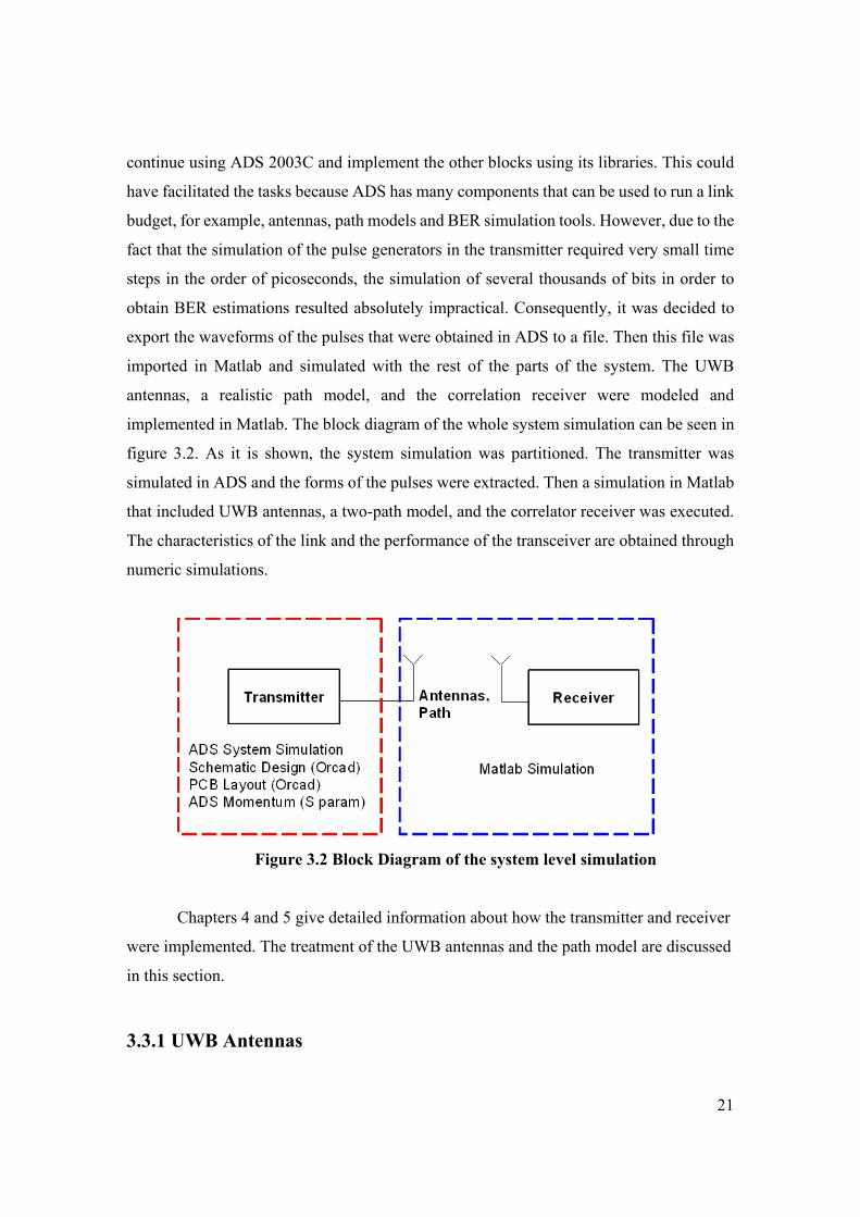
implemented in Matlab. The block diagram of the whole system simulation can be seen in
figure 3.2. As it is shown, the system simulation was partitioned. The transmitter was
simulated in ADS and the forms of the pulses were extracted. Then a simulation in Matlab
that included UWB antennas, a two-path model, and the correlator receiver was executed.
The characteristics of the link and the performance of the transceiver are obtained through
numeric simulations.
Figure 3.2 Block Diagram of the system level simulation
Chapters 4 and 5 give detailed information about how the transmitter and receiver
were implemented. The treatment of the UWB antennas and the path model are discussed
in this section.
3.3.1 UWB Antennas
22
The selection of the UWB antenna is extremely critical for the performance of the
radio. In general, the design of wideband antennas capable of achieving flat frequency
responses of several Gigahertz is a very difficult task for several reasons. To understand
these issues, it is helpful to establish a comparison between UWB signals and narrowband
signals. First, UWB signals show problems that narrowband signals do not have or are
unimportant. Normally, in narrowband signals, the antennas are designed to work at a fixed
frequency. At this frequency, these antennas should present the highest gain (S21) and the
lowest return loss (S11). Besides, narrowband signals present almost constant free-space
Friis attenuation.
On the other hand, an UWB antenna should have a bandwidth of a few Gigahertz.
Achieving low return losses for such a channel bandwidth is extremely difficult. In
addition, the Friis attenuation, which follows the f-2 law, shows characteristics of a low
pass filter in the UWB band. The upper limit of the band at 10.6GHz is attenuated 11dB
more than the lower limit at 3.1GHz [11].
In general, the performance of UWB antennas can be characterized focusing on
three parameters that are the main mechanisms of losses in the link: the pattern of the
antenna, the Friis transmission formula, and the port reflection. Furthermore, it is of
particular interest the impulse responses of the antennas due to the fact that they are
comparable to the UWB pulses. Consequently, the transmitted signal is altered by the
UWB antennas and a new waveform of the pulse needs to be processed in the receiver.
Instead of investigating the behavior of an UWB antenna separately, it is better to
know the complete effect of both the transmitter’s and receiver’s antennas together as a
block. Then the return loss and the gain of different antennas can be compared. For
example, in figure 3.3 it is possible to see the gain S21 and the impulse response of a link
using omni-directional monopole antennas centered around 5GHz.

23
Figure 3.3 Frequency and Impulse Response of the monopole antennas [8]
Two interesting things can be noted here. First, the cascaded antennas behave as a
filter that will modify and degrade the transmitted pulses. Next, the impulse response of the
antenna is by itself larger than the width of the generated UWB pulse. Hence, the
convolution between them will result in a change of the shape of the pulse and additional
ringing. The amount of ringing in the UWB pulses imposes limits to the minimum
separation between pulses in order to avoid superposition, and hence, interference.
The return loss, which is presented in figure 3.4, shows that the antennas will
irradiate effectively at 5GHz and at 17GHz. Furthermore, the cascaded antennas have an
acceptable return loss below -10dB over a bandwidth of less than 1 GHz. On the other
hand, for a great deal of the UWB spectrum, most of the return losses are well above -10dB,
which means that an unacceptable amount of power would be reflected from the antenna to
the transmitter. In conclusion, the monopole is not a very good candidate for UWB systems
which use bandwidths above 1GHz.
Figure 3.4 Return Loss of the monopole antenna [8]
24
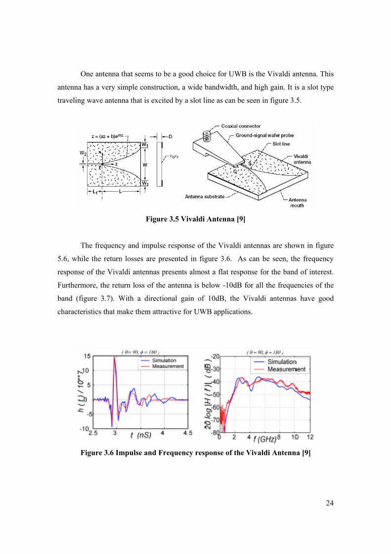
One antenna that seems to be a good choice for UWB is the Vivaldi antenna. This
antenna has a very simple construction, a wide bandwidth, and high gain. It is a slot type
traveling wave antenna that is excited by a slot line as can be seen in figure 3.5.
Figure 3.5 Vivaldi Antenna [9]
The frequency and impulse response of the Vivaldi antennas are shown in figure
5.6, while the return losses are presented in figure 3.6. As can be seen, the frequency
response of the Vivaldi antennas presents almost a flat response for the band of interest.
Furthermore, the return loss of the antenna is below -10dB for all the frequencies of the
band (figure 3.7). With a directional gain of 10dB, the Vivaldi antennas have good
characteristics that make them attractive for UWB applications.
Figure 3.6 Impulse and Frequency response of the Vivaldi Antenna [9]

25
Figure 3.7 Return Loss of the Vivaldi Antenna [8]
The antennas in the present investigation were modeled as a block of cascaded
Butterworth filters. It is assumed that the return losses of the selected antennas are below
-10dB over the band of interest, so most of the energy of the UWB pulses is radiated. The
implementation of the filters considered that the selected antennas were designed to have
maximum gain at the center frequency of the UWB pulses that in this case is 4.0 GHz. Next,
the first characteristic that can be noted is that the antennas have a pronounced high pass
filter behavior from DC to the center frequency. After the center frequency, the frequency
response has a low pass filter characteristic. As a result, the antennas’ frequency response
was modeled using two Butterworth filters. The first filter is a 4th order high pass filter with
a cut frequency of 3 GHz, whereas the second is a 3rd order low pass filter with a cut
frequency of 6 GHz. The impulse and frequency response of the two filters in cascade is
shown in figure 3.8.
Figure 3.8 Modeled Impulse and Frequency response of the UWB antennas
26
Finally, in order to calculate the link budget, the antennas are assumed to be omni
directional radiators with a gain of -3dBi.
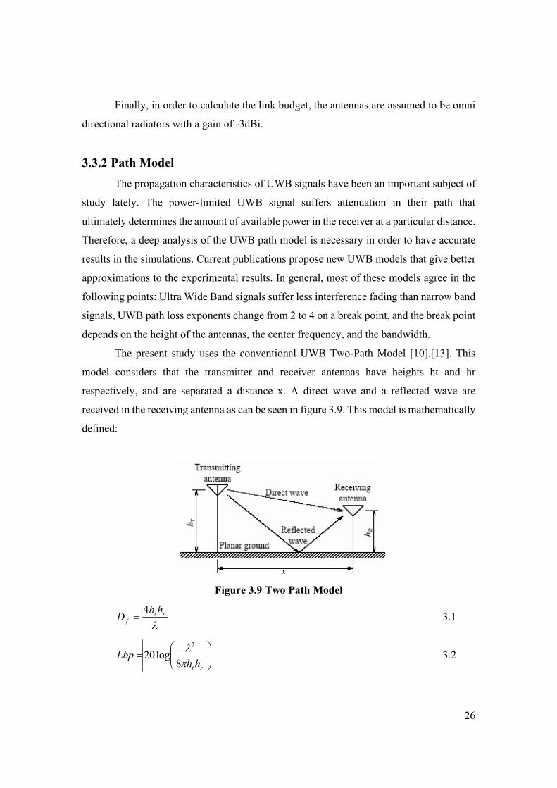
3.3.2 Path Model The propagation characteristics of UWB signals have been an important subject of
study lately. The power-limited UWB signal suffers attenuation in their path that
ultimately determines the amount of available power in the receiver at a particular distance.
Therefore, a deep analysis of the UWB path model is necessary in order to have accurate
results in the simulations. Current publications propose new UWB models that give better
approximations to the experimental results. In general, most of these models agree in the
following points: Ultra Wide Band signals suffer less interference fading than narrow band
signals, UWB path loss exponents change from 2 to 4 on a break point, and the break point
depends on the height of the antennas, the center frequency, and the bandwidth.
The present study uses the conventional UWB Two-Path Model [10],[13]. This
model considers that the transmitter and receiver antennas have heights ht and hr
respectively, and are separated a distance x. A direct wave and a reflected wave are
received in the receiving antenna as can be seen in figure 3.9. This model is mathematically
defined:
Figure 3.9 Two Path Model
λrt
fhh
D4
= 3.1
=
rt hhLbp
πλ
8log20
2
3.2
27
>→
≤→
+=−
DfdDfd
DfdDfd
LbpLossPathLtlog40
log20, 3.3
Where:
Df is the distance of the break point measured from the transmitter’s base
ht is the height of the antenna of the transmitter
hr is the height of the antenna of the receiver
d is the separation of the transmitter and receiver
λ is the wavelength of the frequency of interest
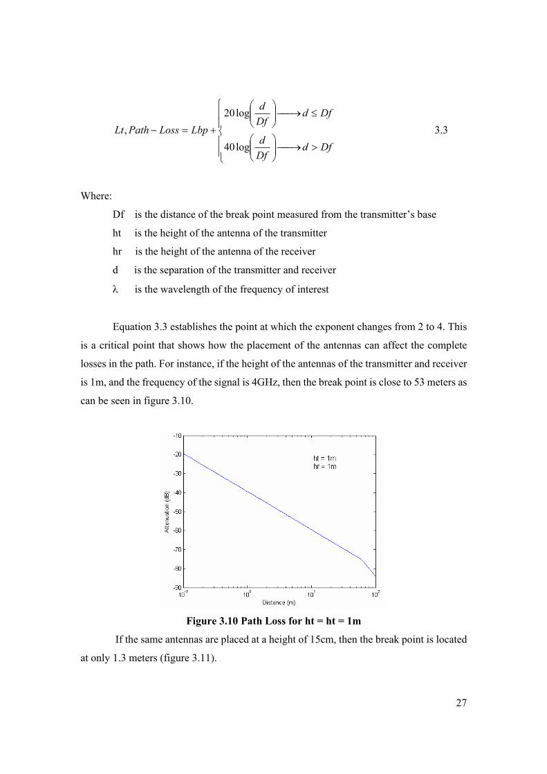
Equation 3.3 establishes the point at which the exponent changes from 2 to 4. This
is a critical point that shows how the placement of the antennas can affect the complete
losses in the path. For instance, if the height of the antennas of the transmitter and receiver
is 1m, and the frequency of the signal is 4GHz, then the break point is close to 53 meters as
can be seen in figure 3.10.
Figure 3.10 Path Loss for ht = ht = 1m
If the same antennas are placed at a height of 15cm, then the break point is located
at only 1.3 meters (figure 3.11).

28
Figure 3.11 Path Loss for ht =hr = 0.15m
This model has the disadvantage that does not specify to which frequency
corresponds λ. However, it has been proposed to use the geometric mean of the low and
high frequency band edges of the UWB pulse:
HL fffm = 3.4
As UWB communications are expected to work at ranges of up to 10m. It is
interesting to note that at this distance if the antennas have a height of 1m and fm is 4GHz,
the resultant path loss is close to 65dB.

29
4 TRANSMITTER DESIGN
4.1 Introduction The present chapter explains the design of the blocks of the DS-UWB transmitter.
Circuit implementations are proposed and commercial components are selected for each
block. Positive Emitter-Coupled Logic (PECL) issues are analyzed. Circuit Schematics
are designed in Orcad Capture and a net list is extracted. Printed Circuit Board layout is
designed in Orcad Layout. Critical RF paths of the pulse generator are exported from the
PCB layout to ADS in order to execute momentum simulations. The design is validated
using ADS and a set of test structures are proposed. Post processing files are generated.
4.2 Pulse Generation Theory A traditional way to generate short pulses is to use step recovery diodes and shorted
transmission lines [4]. Step recovery diodes present the characteristic that if they are
forwarded biased and suddenly they are reversed biased, a low impedance appears until the
charge in the junction is depleted. This means that after changing the biasing from a
positive voltage to a negative voltage, the diode will conduct during a short time, and a
small negative pulse will be available on the output. This phenomenon can be seen in
figure 4.1 which shows the input voltage applied to the diode and its output.
Figure 4.1 SRD Output waveform
30
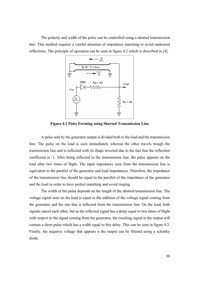
The polarity and width of the pulse can be controlled using a shorted transmission
line. This method requires a careful attention of impedance matching to avoid undesired
reflections. The principle of operation can be seen in figure 4.2 which is described in [4].
Figure 4.2 Pulse Forming using Shorted Transmission Line
A pulse sent by the generator output is divided both to the load and the transmission
line. The pulse on the load is seen immediately whereas the other travels trough the
transmission line and is reflected with its shape inverted due to the fact that the reflection
coefficient is -1. After being reflected in the transmission line, the pulse appears on the
load after two times of flight. The input impedance seen from the transmission line is
equivalent to the parallel of the generator and load impedances. Therefore, the impedance
of the transmission line should be equal to the parallel of the impedance of the generator
and the load in order to have perfect matching and avoid ringing.
The width of the pulse depends on the length of the shorted transmission line. The
voltage signal seen on the load is equal to the addition of the voltage signal coming from
the generator and the one that is reflected from the transmission line. On the load, both
signals cancel each other, but as the reflected signal has a delay equal to two times of flight
with respect to the signal coming from the generator, the resulting signal in the output will
contain a short pulse which has a width equal to this delay. This can be seen in figure 4.3.
Finally, the negative voltage that appears n the output can be filtered using a schottky
diode.

31
Figure 4.3 Positive Pulse Generator
4.3 Pulse Generator Design A monocycle generator with a shape similar to a first derivate of the Gaussian pulse
can be designed using the technique described in the previous section and another shorted
transmission line with the same impedance and length as the first one. This configuration is
shown in figure 4.4.
Figure 4.4 Monocycle Generator
The second shorted stub will reflect an inverted form of the pulse which will appear
on the load after a delay equal to the width of the original pulse. As a result, the waveform
of the pulse on the output will resemble the first derivative of the Gaussian pulse. The
attenuators are used to control the impedance and reduce the effect of undesired
reflections.
In order to design a pulse that accomplishes the spectrum characteristics specified

32
by the FCC, the desired pulse should have a bandwidth of at least 500 MHz inside the
3.1GHz - 10.6GHz band. Hence, the shorted stubs have to be dimensioned accordingly.
Analytically, the delay that a pulse experiments inside the short stub is equal to two
times of flight, or:
Tfd 2= 4.1
Where:
d is the delay of the pulse inside the stub
Tf is the time of flight
The time of flight is calculated using:
vLTf =
4.2
Where:
L is the length of the transmission line
v is the phase velocity inside the transmission line
The velocity of a signal inside a microstrip line is equal to:
e
cvε
= 4.3
Where:
c is the speed of light
εe is the equivalent permittivity of the medium (air, and substrate)
So, the delay of the pulse in the short stub can be expressed as:
cL
d eε2=
4.4
The pulse width of the first derivative of a Gaussian pulse obtained after the second
short stub is 2d, and its center frequency is 1/2d. The -3dB bandwidth is also 1/2d, and the
-10db bandwidth is almost 1/d.
33
Consequently, all the parameters that are needed to create the monocycle are
included in equation 4.4. The parameter εe depends on the εr of the substrate selected for
this application. Once the PCB’s substrate is chosen, only the lengths of the short stubs
have to be determined.
For the case of the UWB transmitter presented in this study, the selected substrate
was the ROGERS 4350 with a thickness of 0.25mm. This material has a dielectric constant
εr equal to 3.48 and a very low loss tangent equal to 0.004. The ROGERS family of
substrates presents an accurate εr which is repetitive over a large range of frequencies, and
is suitable for high frequency RF applications.
After selecting the substrate, the only parameter to be found was the length of the
short stubs. As a result, the center frequency and the bandwidth depend directly on the
manipulation of the length of the stubs. Then, a study to select a preliminary location of the
center frequency was carried out.
There are a few considerations that must be done in order to select the center
frequency. First, due to characteristics of the channel, higher frequencies show larger
attenuation than the lower ones. Besides, the design of the RF circuitry at higher
frequencies up to 10GHz is complex, and requires components that may not exist in the
market yet, or are very expensive. Furthermore, the frequency response of most of the
antennas that have been analyzed presents a larger attenuation for higher frequencies. As a
result, a center frequency close to 4GHz was selected to execute preliminary simulations.
The pulse width of the monocycle for this center frequency is 2d = 1/4GHz equal to
200ps. Thus, using equation 4.4 it is possible calculate the length of the short stubs which
are 320 mIn (8mm).
In order to analyze the previous calculation, a system simulation was executed
using ADS. The simulation was done using time-domain transient and Fourier analysis. As
there were no libraries including self recovering diodes and schottky diodes, a search on
commercial components was done. It was found that Aeroflex Metelics have self recovery
diodes that can be used in these applications [5]. This company has a large list of self
recovering diodes targeted to RF applications. After reading several data sheets, it was
decided to select the MM840 diode because it has the lowest transition time and was
designed for Surface Mount Design applications (SMD). The data sheet with all the

34
characteristics of this diode was used to create the component model in ADS. Likewise, the
schottky diode SMSD6004 was selected and an ADS model was created. Shorted stubs, a
square wave generator, ideal attenuators, and resistors were used from libraries available
with the program.
During the simulation, the lengths of the shorted stubs were tuned until the center
frequency was close to 4GHz. It was found that lengths of 350mIn achieved a correct
center frequency of 4GHz. The simulation results can be seen in figure 4.5.
Figure 4.5 Output of the monocycle generator (Ideal components)
As can be seen, the spectrum of the output of the circuit resembles the one shown in
figure 2.1. Nevertheless, the previous simulation was done using ideal 3dB attenuators, and
ideal connections. In reality, the attenuators are built using resistors in π or T
configurations which have parasitic characteristics and that also are connected by
transmission lines. The present study used attenuators with a π configuration that are equal
to the 3dB attenuator that is shown in figure 4.6.

35
R21294
R20294
R17
17.8
Figure 4.6 3dB Attenuator using a π configuration
In order to have a more accurate result, it was executed a circuit level simulation
taking in account all these issues. The parasitic effects of the resistors depend on their size
and the operating frequency. Furthermore, the selection of the size of the resistors requires
the consideration of the maximum power they will handle and also the difficulty of
mounting them on the prototype.
The sizes of SMD resistors are commonly given in inches, for example a 1206
resistor has a size of 0.12 x 0.06 inches. The circuit of the pulse generator was simulated
using sizes: 0805, 0603 and finally 0402. The two first sizes caused a degradation of the
spectrum of the output that was not acceptable at high frequencies. In order to understand
this phenomenon, the S parameters of 3dB attenuators using these sizes were extracted and
plotted. The S21 parameter for the 0603 resistor size is presented in figure 4.7. As can be
seen, instead of having a constant -3dB gain, this attenuator shows a low pass filter curve
frequency response.
Figure 4.7 S21 parameter of the attenuator using 0603 resistors
The attenuators that were made of 0402 resistors showed, on the other hand, a
better frequency response. The circuit of the monocycle generator was simulated using
these resistors and the output of the circuit can be seen in figure 4.8.

36
Figure 4.8 Output of the monocycle generator using 0402 resistors
Compared to the ideal generator shown in figure 4.5, the output of the circuit using
0402 resistors shows larger attenuation at higher frequencies. Nonetheless, it can be noted
that most of the energy of the pulses is still located around the center frequency, and has a
3dB bandwidth of approximately 3 GHz.
Figure 4.8 was studied to know if the pulse generator’s implementation using 0402
resistor satisfies the spectral requirements. There are a number of issues that must be
considered. First, it has to be noted that the output of the monocycle generator will be
connected to the transmitter antenna. Most of the antennas that have been analyzed for
UWB applications in previous literature show frequency responses that are similar to band
pass filters. Next, due to the Friis attenuation in the air, high frequency components will
suffer higher attenuation than the lower frequency components. As a result, the
monocycles will be band-pass filtered and its shape will be modified. In addition, although
the available bandwidth for UWB granted by the FCC is 7.5GHz, it does not mean that the
pulses should use the whole bandwidth. As a matter of fact, the channel to be processed in
the receiver should be as small as possible in order to keep the noise floor in the lowest
possible level and improve the sensibility.

37
Figure 4.8 shows that most of the energy of the monocycles is contained around 4
GHz, close to the lower border of the band (3.1GHz). This helps to obtain a low Fris
attenuation. However, it also causes that part of the energy of the pulses be under 3.1GHz,
and may cause interference problems to adjacent channels. This situation can be
compensated due to the filtering that is done by the antenna.
In conclusion, the last simulation showed that this circuit can be used to generate
monocycles that enter in the UWB definition. However, a further momentum simulation of
the layout was needed to validate these results.
4.4 Transmitter Schematics The circuit schematics of the transmitter were designed in Orcad 9.1. These
schematics are included at the end of the report and are composed of two pages. The first
page shows the pulse generators and the RF switch whereas the second page shows the
oscillator, voltage regulators and connectors.
The 100MHz oscillator is a JITO 2P5AF, made by Fox Eletronics. The device is
available with several options. In this project it was important to have the rise and fall times
as lower as possible, so a model with positive emitter coupled logic (PECL) output was
selected since it has better speed performance than the normal HCMOS. The differential
output of the oscillator is connected to a differential fanout buffer MC10EL11 which has
two differential ECL outputs with better current capability. The PECL output of the
oscillator is connected to the input of the buffer through resistors R27, R28, R30, R32, R33,
and R34 in order to create appropriate terminations and avoid reflections. The output Q0 of
the buffer is connected in an AC coupling configuration through resistors R29, R31 and
capacitors C13, C14. These signals are labeled POS_IN and NEG_IN, and are connected to
the positive and negative pulse generators. The output Q1 of the buffer is connected to a
SMA connector that is used to test the oscillator.
The circuit uses two voltage sources: +5V and -5V. The first one is implemented
using a National semiconductor LM2937 Low Dropout Regulator which is capable of
supplying up to 500mA of load current with an input of 6-26V. The -5V supply is
implemented using a LM2661 Switched Capacitor Voltage Converter which is capable of
handle up to 100mA.
38
The positive and negative pulse generators use the same circuit with minimum
variations. The positive generator receives the 100MHz square signal POS_IN and
amplifies it using an Intersil EL5166 amplifier. The gain of this amplifier is set to 2 using a
non-inverting configuration. The output of the amplifier is ac coupled through a capacitor
and connected to the first 3dB attenuator. This attenuator is used to protect the low
impedance output of the amplifier and also to control and minimize reflections in the path.
Next, the output of this attenuator is connected to the anode of the SRD diode, and the
cathode is connected to the first shorted stub. A second 3dB attenuator is placed here
before the schottky diode to minimize the reflections. The output of the schottky diode is
connected to another 3dB attenuator before the second shorted stub. Finally, after the
second shorted stub, the signal is connected to the input of the RF switch.
The negative pulse generator has the same configuration but uses the NEG_IN
100MHz square signal, and the SRD and schottky diodes are inverted.
The selected RF switch is a Minicircuits M3SWA-2. This device is a SMD model
designed to operate up to 4.5 GHz with a TTL digital input selector. Unfortunately it was
not possible to find a better switch to use in the design. Minicircuits offers other switches
up to 5.0 GHz, but they are packaged in high-isolation metallic boxes with RF connectors
and are designed for microwave circuits mounted in cases. In addition, the switching speed
of the commercially available switches is low when compared with the requirements of the
UWB signals. In fact, these devices were not designed for switching at high speeds, and as
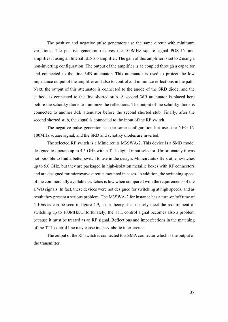
result they present a serious problem. The M3SWA-2 for instance has a turn-on/off time of
5-10ns as can be seen in figure 4.9, so in theory it can barely meet the requirement of
switching up to 100MHz.Unfortunately, the TTL control signal becomes also a problem
because it must be treated as an RF signal. Reflections and imperfections in the matching
of the TTL control line may cause inter-symbolic interference.
The output of the RF switch is connected to a SMA connector which is the output of
the transmitter.
39
Figure 4.9 Timing diagram of the RF switch M3SWA-2 [7]
4.5 Transmitter Layout Once the schematics of the transmitter were finalized, the footprint’s references
were assigned to every component and a netlist was extracted. Afterwards, this netlist was
imported in Orcad Layout Plus V9.1 and the layout process started. The first task was to
determine an optimum placement of the components. This was achieved taking in account
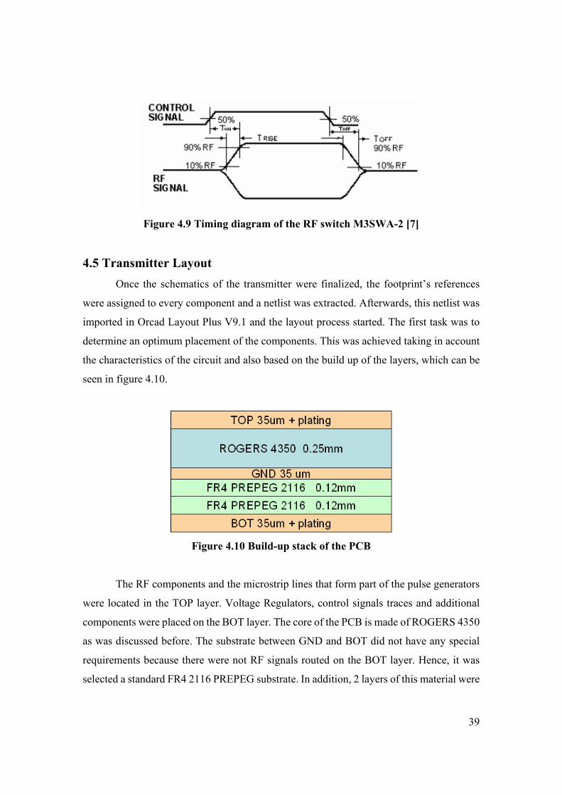
the characteristics of the circuit and also based on the build up of the layers, which can be
seen in figure 4.10.
Figure 4.10 Build-up stack of the PCB
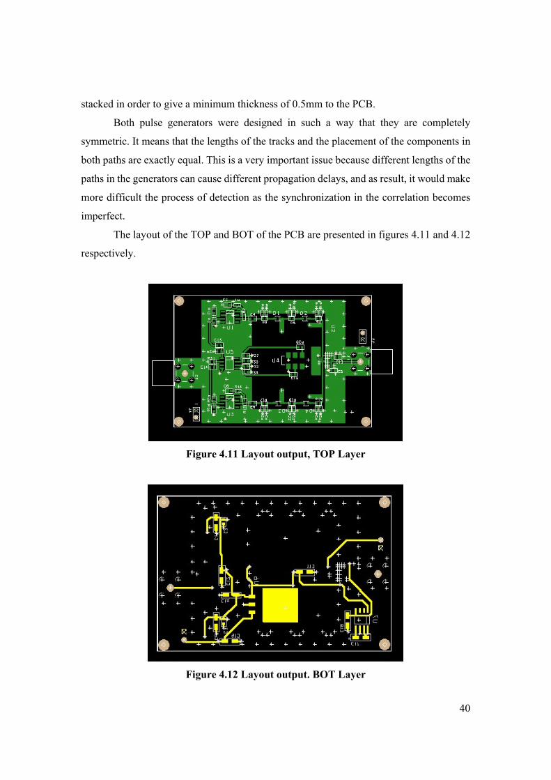
The RF components and the microstrip lines that form part of the pulse generators
were located in the TOP layer. Voltage Regulators, control signals traces and additional
components were placed on the BOT layer. The core of the PCB is made of ROGERS 4350
as was discussed before. The substrate between GND and BOT did not have any special
requirements because there were not RF signals routed on the BOT layer. Hence, it was
selected a standard FR4 2116 PREPEG substrate. In addition, 2 layers of this material were
40
stacked in order to give a minimum thickness of 0.5mm to the PCB.
Both pulse generators were designed in such a way that they are completely
symmetric. It means that the lengths of the tracks and the placement of the components in
both paths are exactly equal. This is a very important issue because different lengths of the
paths in the generators can cause different propagation delays, and as result, it would make
more difficult the process of detection as the synchronization in the correlation becomes
imperfect.
The layout of the TOP and BOT of the PCB are presented in figures 4.11 and 4.12
respectively.
Figure 4.11 Layout output, TOP Layer
Figure 4.12 Layout output. BOT Layer
41
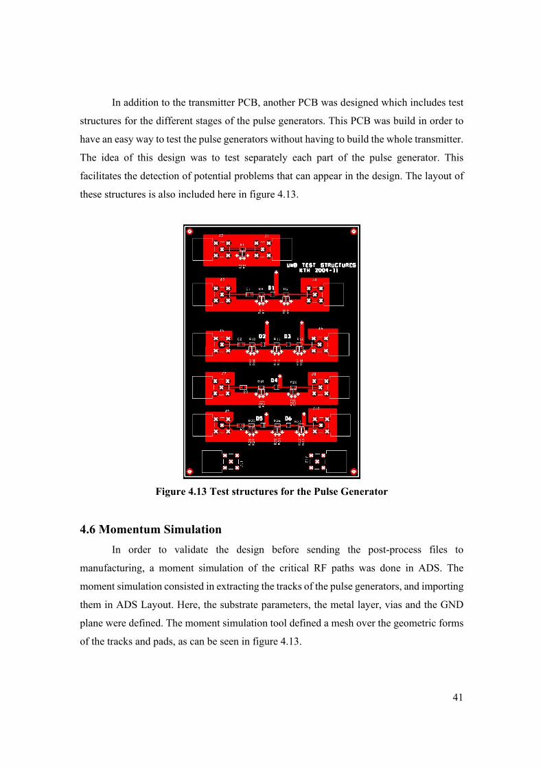
In addition to the transmitter PCB, another PCB was designed which includes test
structures for the different stages of the pulse generators. This PCB was build in order to
have an easy way to test the pulse generators without having to build the whole transmitter.
The idea of this design was to test separately each part of the pulse generator. This
facilitates the detection of potential problems that can appear in the design. The layout of
these structures is also included here in figure 4.13.
Figure 4.13 Test structures for the Pulse Generator
4.6 Momentum Simulation In order to validate the design before sending the post-process files to
manufacturing, a moment simulation of the critical RF paths was done in ADS. The
moment simulation consisted in extracting the tracks of the pulse generators, and importing
them in ADS Layout. Here, the substrate parameters, the metal layer, vias and the GND
plane were defined. The moment simulation tool defined a mesh over the geometric forms
of the tracks and pads, as can be seen in figure 4.13.

42
Figure 4.13 Momentum’s simulation, mesh creation
Afterwards, ADS calculated the S parameters of the paths for a broad range of
frequencies of interest, and generated a component part to be imported within the ADS
Schematics. Then the circuit was simulated again using realistic estimations of the S
parameters of the tracks and models for the capacitors and resistors. The ADS schematics
of the circuit can be seen in figure 4.14
Figure 4.14 ADS Circuit simulation
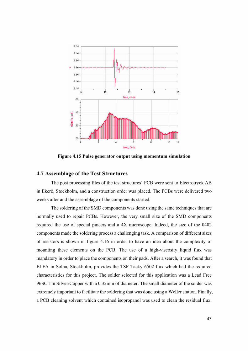
The result of the last simulation is presented in figure 4.15. Here it is possible to see
that the pulse has degraded and presents ringing. The frequency response, however, shows
that most of the energy is still contained inside the UWB band, and as a result, the pulse can
be used for this application.
43
Figure 4.15 Pulse generator output using momentum simulation
4.7 Assemblage of the Test Structures
The post processing files of the test structures’ PCB were sent to Electrotryck AB
in Ekerö, Stockholm, and a construction order was placed. The PCBs were delivered two
weeks after and the assemblage of the components started.
The soldering of the SMD components was done using the same techniques that are
normally used to repair PCBs. However, the very small size of the SMD components
required the use of special pincers and a 4X microscope. Indeed, the size of the 0402
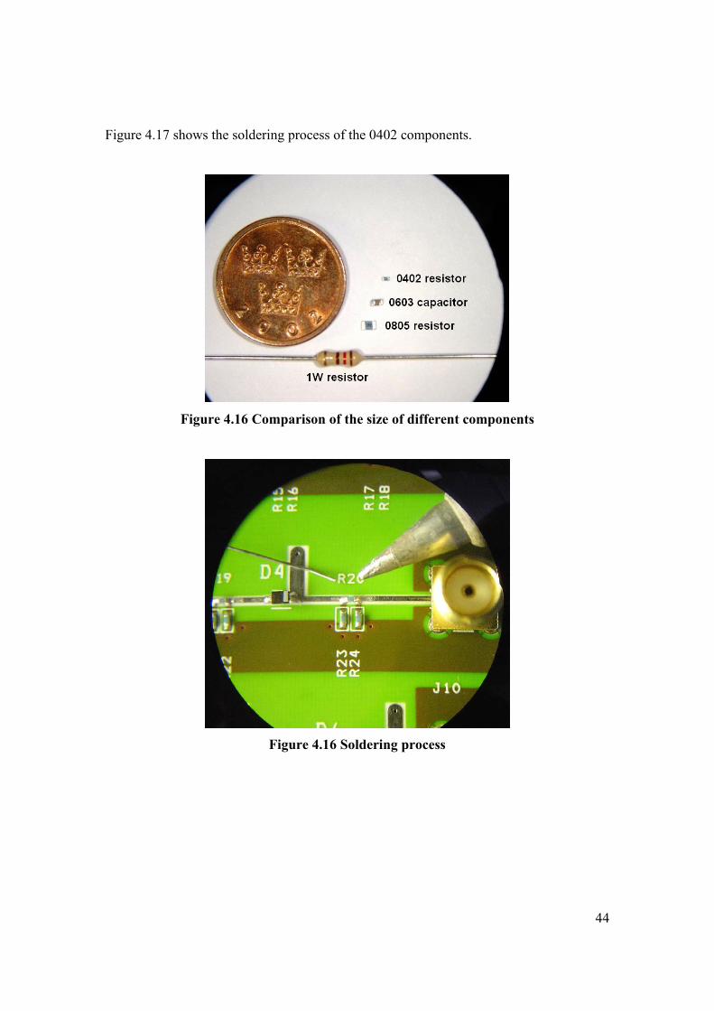
components made the soldering process a challenging task. A comparison of different sizes
of resistors is shown in figure 4.16 in order to have an idea about the complexity of
mounting these elements on the PCB. The use of a high-viscosity liquid flux was
mandatory in order to place the components on their pads. After a search, it was found that
ELFA in Solna, Stockholm, provides the TSF Tacky 6502 flux which had the required
characteristics for this project. The solder selected for this application was a Lead Free
96SC Tin Silver/Copper with a 0.32mm of diameter. The small diameter of the solder was
extremely important to facilitate the soldering that was done using a Weller station. Finally,
a PCB cleaning solvent which contained isopropanol was used to clean the residual flux.
44
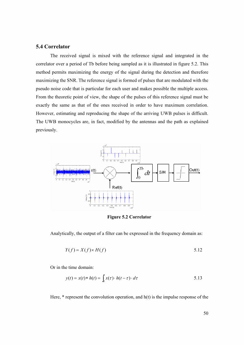
Figure 4.17 shows the soldering process of the 0402 components.
Figure 4.16 Comparison of the size of different components
Figure 4.16 Soldering process

45
5 RECEIVER DESIGN 5.1 Introduction This chapter describes the concept of the correlator receiver. First, a study of the
noise in the receiver is carried out in order to know if the RF front-end requires an LNA or
not. Afterwards, the parts of the correlator are described in detail. The selection of a
sub-optimum template for the correlation is discussed. Finally, it is analyzed the effect of
the jitter in the correlation process.
5.2 Receiver RF Front-End The receiver front-end of the UWB radio can be seen in figure 5.1. The simulation
of the correlation receiver front-end consisted in the following steps. First, the received
UWB signal is added with additive white gaussian noise AWGN. Then the signal is
amplified and mixed with a template signal. Afterwards, the signal is integrated over a
period of a bit time, and sampled. The sampling of the signal is the last step of the receiver
front end. Then, a 1 bit ADC which can be a comparator to zero takes the output of the front
end and produces a digital output that is fed to the baseband processing.
Figure 5.1 Receiver Front-End
5.3 Noise Analysis and LNA requirement The power of the noise added to the received signal at the input depends on a
number of considerations. First, it is important to note that if there are not interference

46
signals in the UWB band, the only noise present in the input is thermal noise. This noise
passes through all the stages in the chain and is further degraded. The amount of
degradation of the noise that each stage introduces is quantified by the Noise Figure
parameter which is defined as:
out
in
SNRSNR
NF = 5.1
In this study, instead of considering the noise figure for each block separately, it is
assumed that the noise figure of the whole Front End referred to the input is known. This
parameter permits to calculate directly the sensitivity of a system and is obtained using the
Friis equation [14] for the NF which states:
)1(11
21 ...
1....
1)1(1
−
−++
−+−+=
mpp
m
p AANF
ANF
NFNF 5.2
Where:
NF is the Noise Figure of the receiver
NFi is the Noise Figure of the stage i
Api is the Gain of the stage i
The thermal noise referred to the input of a radio system is called noise floor [14].
When the antenna is matched it is defined as:
BNFHzdBmNoise log10/174 ++−= 5.3
Where:
Noise is the power of the noise in the channel (dBm)
NF is the Noise Figure of the receiver (dB)
B is the bandwidth of the channel (HZ)
In addition, the sensibility of a radio system is defined as the minimum level of

47
power that the receiving signal must have in order to accomplish a minimum SNR or:
minmin, SNRNoisePin += 5.4
minmin, log10/174 SNRBNFHzdBmPin +++−= 5.5
Where:
Pin,min is the minimum power of the received signal (dBm)
SNRmin is the min. signal to noise radio to keep the specifications BER (dB)
Also, it is important to know the power of the received signal that is defined as:
LtGrGtPtPin −++= 5.6
Where:
Pin is the available power of the received signal (dBm)
Pt is the power of the transmitted signal (dBm)
Gt is the gain of the antenna of the transmitter (dB)
Gr is the gain of the antenna of the receiver (dB)
Lt is the path loss for a specific distance and heights of the antennas (dB)
Finally, it is important to note that UWB systems use spread spectrum techniques,
and therefore, they have processing gain. This gain is defined as the ratio of the spread
bandwidth (the channel bandwidth) to the bandwidth of the information signal at the
receiver output [15]. Assuming that the bandwidth of the information signal is the same as
the bitrate (which is expected after the integration in the correlator over a period of Tb),
then the following equation can be used:
=
rBPG log10 5.7
Where:
B is the total bandwidth of the UWB signal (Hz)
r is the bit rate of the system (bps)

48
For the case of UWB systems, Ns pulses are integrated every Tb seconds, so the bit
rate can be rewritten as r = 1/NsTf, where Tf is the pulse repetition time. In addition, the
bandwidth B of the UWB pulse is almost equivalent to 1/τ, where τ is the pulse width.
Then, the UWB processing gain can be rewritten as:
)log(10log10 Sf N
TPG +
=
τ 5.8
PG is a parameter that influences the SNRmin required to maintain a specific
performance. Other parameters are the type of modulation, multiple access technique,
efficiency of the detection and the number of users that share the channel. SNRmin can be
obtained using equations 2.9 or 2.13 for TH-UWB and DS-UWB respectively. Thus,
equation 5.5 is expressed as:
),(log10/174 minmin,, NuPGSNRBNFHzdBmP UWBin +++−= 5.9
Now an analysis is carried out to know whether a LNA is required or not. From
equation 5.2 it is clear that the first stage in the path is the most important in order to
maintain the noise figure as low as possible. In addition, 5.13 suggest that the noise figure,
the bandwidth of the system, and the processing gain can be modified to reduce the
sensibility of the system. These three parameters can be traded off to obtain the sensibility
required for a specific SNR.
The channel bandwidth of the system is defined by the bandwidth of the UWB
pulse, and also in the absence of other filters, by the frequency response of the antennas.
The processing gain depends on the bit rate and the pulse repetition rate, which are
parameters that depend on the target application. It is clear from 5.8 that high data rates will
not have high processing gains. In fact, the reduction of Tf or Ns in order to increase the bit
rate of the system will result in a reduction of processing gain.
Consequently, the only improvement that can be done from the architecture point
of view is to reduce the overall noise figure. This is a very important issue for the UWB
radio due to the fact that the transmitted power is very limited (in the order of -9dBm) and

49
the expected losses in the path at distances where high data rates are expected, are
predicted to be high by the model simulations discussed in section 3.3.2. For instance, the
path loss attenuation can reach easily 80 dB at 10m depending on the location of the
antennas, as shown in figure 3.11. This situation is further aggravated when the noise floor
is increased due to multi-user activity. Therefore, in order to improve the sensitivity of the
system and match the SNR specifications, the first stage should always be a LNA.
To illustrate this situation the figures of noise of two front ends are calculated, one
using a LNA as the first stage and other using directly a Gilbert-cell mixer. The
specifications of the Mixer and LNA are described in table 5.1. It is assumed that the
integrator is ideal and do not affect the noise calculations.
Noise Figure (dB) Gain (dB)
LNA 3 10
Mixer 12 10
Table 5.1 Noise Figure and Gain of LNA and Mixer
The noise figure of the receiver using the LNA is near to 5 dB. On the other hand,
the noise figure of the receiver using the mixer in the input is at least 12 dB. This 7 dB
difference in the sensitivity of the receiver affects directly the maximum range of the link
as can be shown when equations 5.6 and 5.9 are combined in order to calculate the
maximum path losses that can be tolerated to maintain a fixed SNR:
UWBinMAX PGrGtPtLt min,,−++= 5.10
),(log10/174 min NsPGSNRBNFHzdBmGrGtPtLtMAX −−−+++= 5.11
In conclusion, the thermal noise level on the receiver is calculated using equation
5.3. The noise figure of the receiver is assumed to be a known parameter that is obtained
using equation 5.2. Finally, the front end should include a LNA in the first stage to keep the
noise power as low as possible.
50
5.4 Correlator
The received signal is mixed with the reference signal and integrated in the
correlator over a period of Tb before being sampled as it is illustrated in figure 5.2. This
method permits maximizing the energy of the signal during the detection and therefore
maximizing the SNR. The reference signal is formed of pulses that are modulated with the
pseudo noise code that is particular for each user and makes possible the multiple access.
From the theoretic point of view, the shape of the pulses of this reference signal must be
exactly the same as that of the ones received in order to have maximum correlation.
However, estimating and reproducing the shape of the arriving UWB pulses is difficult.
The UWB monocycles are, in fact, modified by the antennas and the path as explained
previously.
Figure 5.2 Correlator
Analytically, the output of a filter can be expressed in the frequency domain as:
)()()( fHfXfY ×= 5.12
Or in the time domain:
τττ dthxthtxtyt
⋅−⋅=∗= ∫0 )()()()()( 5.13
Here, * represent the convolution operation, and h(t) is the impulse response of the

51
filter. Accordingly, the signal in the input of the LNA can be estimated through the
convolution of the transmitted signal and the impulse response of the antennas. Figure 5.3
shows this operation both in the frequency and time domain.
Figure 5.3 convolution of monocycle and antennas impulse response
The result of the convolution shows the change of the shape that the monocycles
experience before the LNA. Assuming that the bandwidth of the LNA is flat enough in the
whole band, and that its 1dB compression point is high enough, then no further degradation
of the pulse is expected. Accordingly, the reference template in the receiver should ideally
have pulses with this shape in order to have optimum correlation.
Generating circuits that produce these filtered versions of the monocycle pulses are
difficult. Hence, a selection of a suboptimal but feasible pulse has to be done. Previous
literature suggests that a sine wave with a frequency equal to the center frequency of the
monocycle pulse can be used [15] and synchronized using an analog PLL. This technique
facilitates the implementation, but it has some drawbacks. In fact, a deep analysis shows
that the pulse repetition time Tf should be a multiple of the period of the sine signal for
DS-UWB. Likewise, Tc should be a multiple of the period of the sine wave for TH-UWB.
In this work it is proposed to correlate the incoming signal with a reference signal
that uses the same monocycles that are generated for transmission. This scheme has the
advantage that does not require another block to generate the reference signal but instead it
uses the same positive pulse generator block that is available in the transmitter chain. This
is a suboptimal solution, and thus, it is necessary to investigate how it affects the
performance of the system. This can be done comparing the outputs of the correlation
52
function of the receiving signal with the ideal template and with the proposed solution.
The correlation function is defined as:
dtthtxR ⋅−⋅= ∫+∞
∞−)()()( ττ 5.14
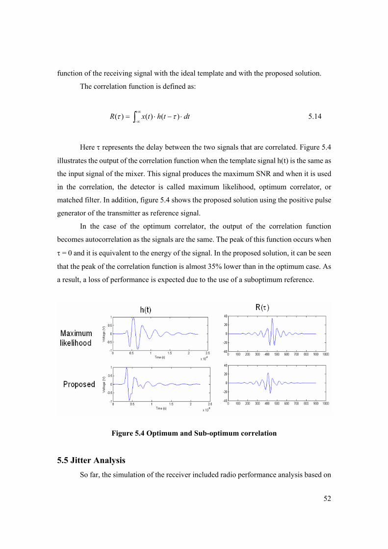
Here τ represents the delay between the two signals that are correlated. Figure 5.4
illustrates the output of the correlation function when the template signal h(t) is the same as
the input signal of the mixer. This signal produces the maximum SNR and when it is used
in the correlation, the detector is called maximum likelihood, optimum correlator, or
matched filter. In addition, figure 5.4 shows the proposed solution using the positive pulse
generator of the transmitter as reference signal.
In the case of the optimum correlator, the output of the correlation function
becomes autocorrelation as the signals are the same. The peak of this function occurs when
τ = 0 and it is equivalent to the energy of the signal. In the proposed solution, it can be seen
that the peak of the correlation function is almost 35% lower than in the optimum case. As
a result, a loss of performance is expected due to the use of a suboptimum reference.
Figure 5.4 Optimum and Sub-optimum correlation
5.5 Jitter Analysis So far, the simulation of the receiver included radio performance analysis based on

53
the assumption that only thermal noise is present. However, UWB impulse radios have
particular problems that are not seen in narrow band radio systems. In fact, the jitter
produced by the oscillators that are used in the pulse generation causes synchronization
problems in the correlation process and becomes a serious issue in UWB systems. The
UWB pulses have very short duration in the order of a few hundred picoseconds as it was
shown in chapter 2 and 4. Accordingly, even small mismatches in the synchronization
process can affect the overall performance of the system.
Therefore, in order to quantify this problem, the block of the correlator is able to
simulate the effect of the phase noise in the oscillators. The oscillator selected for this
project was the JITO 2P5AF whose rms phase noise according to the data sheet is about 15
ps rms. Since both the transmitter and receiver oscillator contributes to the jitter, the total
rms phase noise was set to 21 ps ( 152 × ps).

54
6 SYSTEM SIMULATION AND TEST RESULTS 6.1 Introduction
The DS-UWB transceiver that was proposed in this study was simulated in order to
obtain its performance under an AWGN channel. The objective of this simulation was to
know the signal to noise ratio (SNR) and the bit error rate (BER) of the link at distances up
to 100m using different bit rates. Two simulations were executed in order to compare the
degradation of the performance due to phase noise. The first simulation did not include
jitter in the calculations while the other introduced the jitter effect as described in section
5.5. Next, the results of the measurements of the pulse generator are presented. Finally, a
case study is included to illustrate the multi-user capability of the system.
6.2 System Level Simulations The simulation of the UWB transceiver considers the following characteristics of
the system in order to find the link budget:
System Characteristics
3GHz bandwidth
100 MHz pulse rate
100,50,25,10 Mbps
Height of Tx/Rx antennas = 1m
Transmitter
Tx Antenna Gain: -3dB
Tx Power: -9.2 dBm
Receiver
Rx Antenna Gain: -3dB
Noise Figure: 8 dB
Table 6.1 UWB Link budget
The link budget is calculated for distances that range from 1m to 100m in steps of
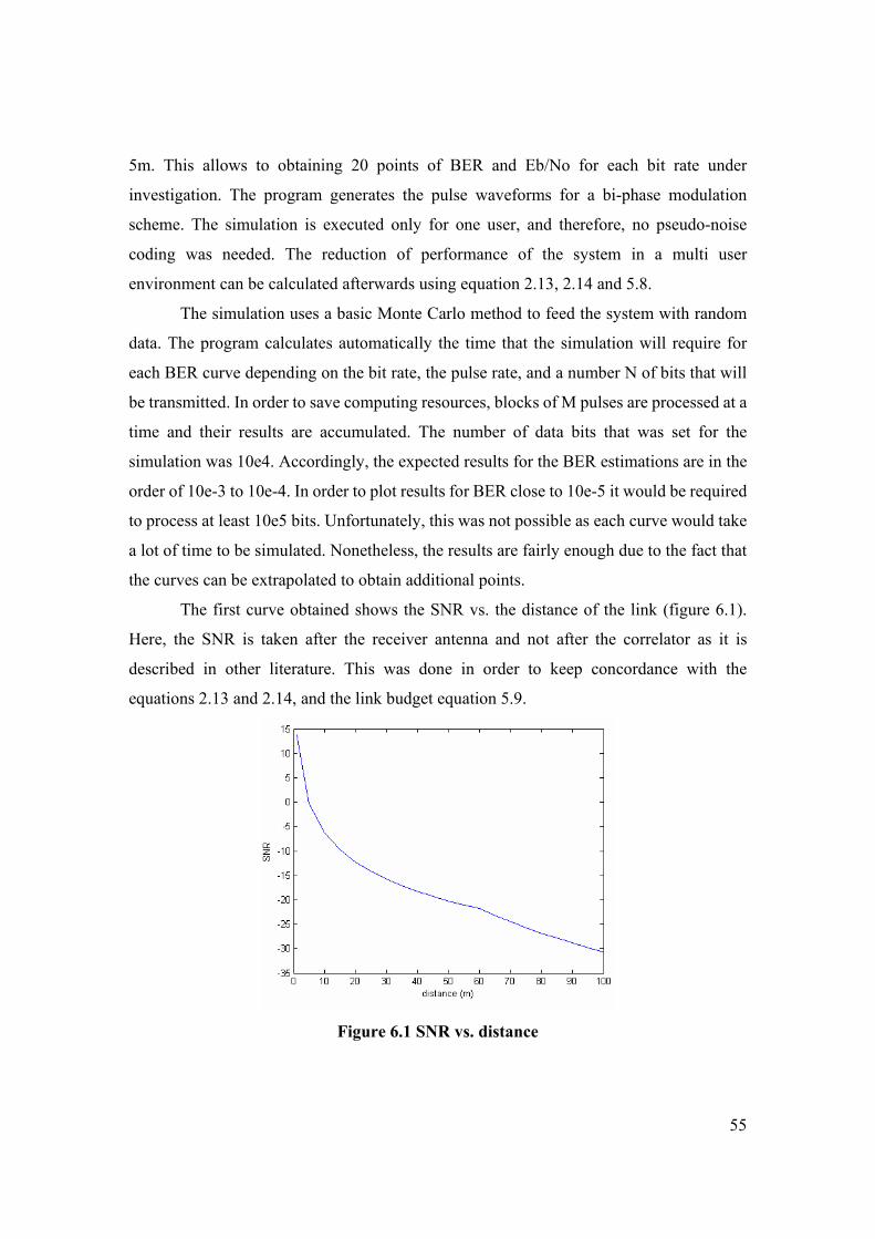
55
5m. This allows to obtaining 20 points of BER and Eb/No for each bit rate under
investigation. The program generates the pulse waveforms for a bi-phase modulation
scheme. The simulation is executed only for one user, and therefore, no pseudo-noise
coding was needed. The reduction of performance of the system in a multi user
environment can be calculated afterwards using equation 2.13, 2.14 and 5.8.
The simulation uses a basic Monte Carlo method to feed the system with random
data. The program calculates automatically the time that the simulation will require for
each BER curve depending on the bit rate, the pulse rate, and a number N of bits that will
be transmitted. In order to save computing resources, blocks of M pulses are processed at a
time and their results are accumulated. The number of data bits that was set for the
simulation was 10e4. Accordingly, the expected results for the BER estimations are in the
order of 10e-3 to 10e-4. In order to plot results for BER close to 10e-5 it would be required
to process at least 10e5 bits. Unfortunately, this was not possible as each curve would take
a lot of time to be simulated. Nonetheless, the results are fairly enough due to the fact that
the curves can be extrapolated to obtain additional points.
The first curve obtained shows the SNR vs. the distance of the link (figure 6.1).
Here, the SNR is taken after the receiver antenna and not after the correlator as it is
described in other literature. This was done in order to keep concordance with the
equations 2.13 and 2.14, and the link budget equation 5.9.
Figure 6.1 SNR vs. distance

56
It is interesting to note that the SNR at 10m is close to -6dB in the absence of other
users. Next, the BER vs. SNR curves were calculated for each bit rate. The first simulation
assumed that the oscillators do not introduce jitter. The curves are shown in figure 6.2.
Figure 6.2 BER vs. SNR without phase noise
The presence of coding gain is appreciable when the bit rate is reduced. This was
expected from the second term of equation 5.8. For instance, there is a reduction of 10dB in
the SNR required to maintain a specific BER for 10Mbps when it is compared to 100Mbps.
The graph also shows that the correlator receiver has a very good performance in an
AWGN channel. Indeed, a 100Mbps link could be established at almost 15m when the
channel is not shared by other users.
The next interesting results that were extracted were the BER vs. Eb/No curves that
can be seen in figure 6.3. The integration of the energy of the pulses and the noise over a
time of Tb resulted in an equal average energy per bit Eb/No for all bit rates. This result is
compared to the curve in figure 2.5 where the BER curve for bi-phase modulation is shown.
To facilitate this comparison, this curve is repeated in figure 6.3 in black color and dotted
line.

57
Figure 6.3 BER vs. Eb/No
The ideal curve of bi-phase demodulation using a matched filter requires more or
less 2 dB less energy per bit than the receiver proposed in this study. This loss is caused by
the imperfect correlation as explained in 5.6.
Next, a new simulation that included the effect of a jitter due to the oscillators was
executed. Figure 6.4 shows the BER vs. SNR for this case. It is immediately noticeable the
effect that the jitter causes at bit rates close to the pulse rate. For 100Mbps, where each
pulse corresponds to one bit, the performance is degraded to a level in which the BER can
not reach 10e-3 for any SNR.
The BER vs. Eb/No curves that include the jitter effect are presented in figure 6.4.
The performance of the system at 100Mbps and 50Mbps is reduced considerably. On the
other hand, the behavior of the 25Mbps and 10Mbps curves is almost the same as in the
previous simulation. These bit rates do not show a reduction in performance when the BER
is larger than 10e-4. In conclusion, if the expected jitter in the correlation is close to 20ps
rms and the target BER is larger than 10e-4, then the system shows certain immunity to
jitter when Ns is larger than 4.

58
Figure 6.3 BER vs. SNR with jitter
Figure 6.4 BER vs. Eb/No with jitter
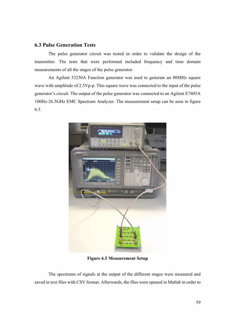
59
6.3 Pulse Generation Tests The pulse generator circuit was tested in order to validate the design of the
transmitter. The tests that were performed included frequency and time domain
measurements of all the stages of the pulse generator.
An Agilent 33250A Function generator was used to generate an 80MHz square
wave with amplitude of 2.5Vp-p. This square wave was connected to the input of the pulse
generator’s circuit. The output of the pulse generator was connected to an Agilent E7405A
100Hz-26.5GHz EMC Spectrum Analyzer. The measurement setup can be seen in figure
6.5.
Figure 6.5 Measurement Setup
The spectrums of signals at the output of the different stages were measured and
saved in text files with CSV format. Afterwards, the files were opened in Matlab in order to

60
analyze and compare the results. The measured spectrum of the UWB pulses is shown in
Figure 6.6. It is interesting to compare this spectrum with the spectrum of the momentum
simulations in Figure 4.15. The measurements show that the spectrum of the UWB pulses
generated by the circuit is better than the spectrum after the momentum simulation. Also,
from the spectrum in figure 6.6 it can be seen that most of the power of the signal is
contained between 2 and 5 GHz.
Figure 6.6 Spectrum
The time measurements of the test structures were performed using an Agilent
Infiniium DCA 86100B Wide Bandwidth Oscilloscope. The oscilloscope required an
external trigger signal in order to synchronize the input. Fortunately, the function generator
has a Sync output which is in phase with the signal output. The measurements were done
and the UWB pulse waveforms were saved in JPEG and text-verbose format. Figure 6.7
shows the output of the Gaussian pulse generator (the output after the second attenuator).
Figure 6.8 shows the output of the first derivate of the Gaussian pulse (the output after the
second short stub). These signals show that the circuit worked as expected. It can be noted
in particular the similarity of the waveform of figure 6.8 with that of figure 2.1. Without
considering the small voltage variations due to ringing, the pulse width is very close to the
200ps target. In addition, it is important to note the presence of 50ps peak-peak jitter in the

61
measurements.
Figure 6.7 Measurement of the Gaussian Pulse Generator
Figure 6.8 Measurement of the First Derivate of the Gaussian Pulse
Figure 6.9 presents the UWB pulse train. Besides the UWB pulses, it is possible to
identify undesired reflections that appear due to imperfect matching.

62
Figure 6.9 UWB Pulse train, measurement
Finally, the train signal was processed in Matlab in order to know the effect of the
filtering done by the antenna of the transmitter. The filtered signal and the UWB emission
mask are shown in figure 6.10. For convenience, the frequency axe has been changed to
logarithmic scale. It can be noted that the signal accomplishes the UWB emission
requirements.
Figure 6.10 Spectrum of the transmitted signal and allowed emission levels

63
6.4 Case Study To illustrate the meaning of the curves presented in section 6.2 and understand how
they can help to design a DS-UWB system, a case study is presented here using the same
general characteristics of the link budget that were described in the table 6.1.
In this case it is established that a system using the DS-UWB impulse radio
described in this project should have a throughput of 10Mbps with a BER of 10-3 at 10m.
Also, no forward error correction coding was performed. We are interested in knowing the
level of the receiving power in the transmitter and the theoretical number of users that the
UWB system can have. It is assumed that power control is possible, so that the receiving
power of the signals of all the users is the same.
First, the power of the receiving signal of one user and the power of the thermal
noise are calculated using equation 5.10 and equation 5.7 respectively.
dBmLtGrGtPtPR 77−=−++=
dBmBNFHzdBmNoise 71log10/174 −=++−=
Then, using the 10Mbps curve, we found the Eb/No point in which the BER is
10e-3, which happens to be at 7dB. Now, equations 2.13 and 5.12 are combined to
establish the relationship between Eb/No, the SNR and the gain of the DS-UWB.
( )dB
dBdB r
BSNRIoEb
+=
( ) ( )NsT
SNRIoEb f
dBdB
log10log10 +
+=
τ
Tf is the period of the pulses and it is equal to 10 ns (1/100MHz). The parameter τ
is the pulse width of the UWB monocycle, which is close to 0.25ns. Ns is the number of
pulses transmitted per bit and is equal to 10 (Ns = 100MHz/10Mbps). Then, replacing these
parameters we have:

64
( ) )10log(1025.10log107 +
+=
nsnsSNR dB
( ) 10167 ++= dBSNR
( ) 19−=dBSNR dB = 0.0123
Where the total power of the noise (interferers + thermal noise) can be calculated:
( ) dBdBdB PnPsSNR −=
dBmdBdBmPndB 58)19(77 −=−−−=
So, the total power of the noise is 13 dB higher than that of the thermal noise. This
implies that the joint power of the interferers is almost 20 times higher than the power of
the thermal noise. Consequently, it is safe enough to continue with the assumption that the
interferers dominate the total power of the noise in the receiver.
Then, finally, the maximum number of users that can use this UWB system is
calculated using equation 2.14:
11−
=uN
SNR
110014.0−
=uN
82=uN

65
7 CONCLUSIONS This thesis has covered the design of a DS-UWB impulse radio using off-chip
components. The radio uses first Gaussian derivative pulses that are modulated using a
bi-phase modulation technique. The pulse rate of the system is 100MHz and the bit rates
under investigation were 100Mbps, 50Mbps, 25Mbps, and 10Mbps. The transmitter and
receiver were divided in functional blocks in order to execute system level simulations.
Afterwards, the transmitter was implemented in both schematics and layout. The pulse
generator circuit, that is the main block of the transmitter, was constructed and tested. The
receiver, on the other hand, was simulated in Matlab due to the fact that its implementation
presented particular difficulties for an off-chip solution. Nevertheless, the performance of
the receiver was estimated through numeric simulations. Finally, a case study for the
multi-user capability was presented.
First, the theory of UWB pulses was analyzed in order to know the properties of
wide band signals. From this analysis, it was concluded that the first derivative of the
Gaussian pulse is a good candidate for UWB applications. Next, baseband modulation
techniques were studied and compared. Bi-phase and PPM modulation can be used in
UWB as they showed better Eb/No performance than other techniques. Bi-phase
modulation was selected for this application due to the fact that it presents better Eb/No
performance and also has relaxed synchronization requirements than PPM. Afterwards,
multi-user methods for UWB were analyzed. Two approaches were found: DS-SS and
TH-SS. DS-SS was selected because it has a better performance at short ranges and also it
is easier to synchronize.
Once the pulse form, modulation, and access techniques were established, a study
of UWB pulse generation was executed. The generation of UWB pulses using shorted
transmission lines and self recovering diodes was chosen because it was a simple and
efficient off-chip implementation. This solution was modified to produce pulses similar to
first derivative Gaussian pulses. The circuit of the pulse generator was simulated using
ADS, and it was found that the size of the SMD resistors has a strong influence and
degrades the frequency response of the pulse generator. However, it was shown that this
situation can be solved if the circuit uses 0402 SMD resistors.
The circuit of the transmitter was implemented both in schematics and layout. In

66
addition, a PCB which includes the pulse generator structures was prototyped to test all the
steps of the monocycle generation. The measurements were successful and showed that the
pulse generator worked correctly. A potential problem was detected in the design of the
transmitter. The device that is responsible of the data modulation is a RF switch that has a
TTL control with a maximum switching time of 5-10ns. Consequently, it may not be able
to switch correctly under the pulse rate specification of 100MHz.
Because an off-chip construction of the receiver resulted impractical, the functional
blocks of the receiver were implemented in Matlab. The correlator receiver structure was
selected as it is far less complex than the RAKE receiver, and hence, showed a more
feasible implementation.
The simulation of the whole system required to include the effect of the antennas
and the path. It was shown that the antennas used in UWB applications are critical
components since they change the shape of the UWB monocycles. This situation
complicates the correlation process as it is difficult to find and reproduce the modified
pulse in the receiver. Likewise, the UBW two path model used in the simulation proved
that the path loss has large variations depending on the location of the antennas. High
losses are predicted when the antennas have small heights.
The whole system was simulated and the BER vs. Eb/No curves were extracted. It
was found that the correlation receiver performed correctly and had curves similar to the
theoretical bi-phase modulation. More interesting, it was also found the reduction of the
performance of the receiver in the presence of jitter. This is a main concern in UWB
systems since the correlation of UWB pulses is degraded when the incoming pulses and the
reference pulses are not perfectly aligned. For a jitter value of 21ps rms and a BER larger
than 10e-4, it was shown that the correlation receiver is not affected when Ns is at least 4.
For higher bit rates, Ns=1,2, the curves show an unacceptable performance.
In conclusion, a DS-UWB impulse radio was designed. The transmitter was
implemented and the pulse generation module was tested. The receiver, on the other hand,
was simulated. Its implementation is more appropriate for an on-chip solution. The
DS-UWB impulse radio with a correlation receiver showed an excellent performance at
low distances and presents a simple and feasible implementation compared to other
solutions.

67
8 FUTURE WORK
The design of the DS-UWB impulse radio resulted to be a large task that was
beyond the limited time of this study. However, the obtained results were very encouraging.
Some of the future tasks that can be done are described here.
The layout of the transmitter was generated and it is ready to send to fabrication. It
was not tested since it was decided to validate first the pulse generation structures using
another PCB. Since the testing of the pulse generator was successful, the next step would
be to test the PCB of the transmitter. In addition, it is suggested a reduction of the oscillator
frequency as it would relax the switching requirements of the RF switch at expenses of
lower bit rates.
The correlation receiver architecture presented in this study can be implemented
on-chip. An LNA with a target bandwidth of 3GHz may be enough for this application.
Besides, a low-power wide-band mixer with a low noise figure needs to be designed. It can
be, for instance, a variant of a Gilbert mixer. The design of other blocks, however, presents
a difficult challenge. The time-delay block that aligns the incoming signal with the local
reference depends on digital bandbase processing in this study. As a result, if an all-analog
solution is wanted, it would be needed to design a circuit that senses the Eb (The voltage
after the integrator). This circuit would act as a phase detector that controls the time delay
block.
Finally, the Matlab code of the correlator receiver can be improved in order to
execute other system level simulations. The implementation of the phase detector/tracking,
for example, may be very useful to find the time that the receiver needs to achieve the pulse
synchronization. Also, other pulse waveforms may be investigated in order to be used as
templates in the correlator. One interesting thing that can be improved in the code is to
include multi-user interference. Accordingly, it could be possible to confirm the theoretic
multi-user capability.

68
9 LIST OF SYMBOLS AND ABBREVIATIONS
9.1 Symbols B Bandwidth of the channel
c Speed of light
εo Electric permittivity of the vacuum
Eb Average energy per bit
λ Wavelength
No Spectral density of the noise
Ns Number of transmitted pulses per bit
Nu Number of users
Pin,min Sensitivity of the receiver
r Bit rate of the system
Rx Receiver
τ Pulse width
Tb Time of one bit
Tf Pulse repetition period
Tc Slot of time within TF used in TH
Tx Transmitter
9.2 Abbreviations ADS (Agilent) Advanced Design System
AWGN Additive White Gaussian Noise
BER Bit Error Rate
bps bits per second
BPSK Bi-phase shift keying, or binary phase shift keying
CDM Code Division Multiplexing
DS Direct Sequence
FCC Federal Communications Commission
FDM Frequency Division Multiplexing

69
LPD Low Probability of Detection
NF Noise Figure
OFDM Offset Frequency Division Multiplexing
OOK On-Off Keying
OPM Orthogonal Pulse Modulation
PAM Pulse Amplitude Modulation
PCB Printed Circuit Board
PECL Positive Emitter Coupled Logic
PPM Pulse Position Modulation
RF Radiofrequency
SNR Signal to Noise Ratio
SS Spread Spectrum
TDM Time Division Multiplexing
TH Time Hopping
UWB Ultra Wide Band
70
10 REFERENCES:
[1] M. Z. Win, R. A. Scholtz, “Impulse Radio: How it works,” IEEE Communication
Letters, Vol. 2 No.1,pp.10-12,January 1998.
[2] B. Mihai, “Ultra Wide Band Technologies,” Ad Hoc Mobile Wireless Networks,
Research Seminar on Telecommunication Software, autumn 2002.
[3] B. Mielczarek, M. Wessman, A. Svensson, “Performance of Coherent UWB Rake
Receivers using different Channel Estimators,” IWUWBS 2003, June 2003
[4] A. Kuthi, M. Behrend, T. Vernier,M. Gundersen, “Bipolar Nanosecond Pulse
Generation using Transmission Lines for cell electro-manipulation,” 26th International
Power Modulator Symposium, May 23, 2004.
[5] A. Orndorff, “Transceiver Design for Ultra-Wideband Communications”, May 20,
2004, < www.scholar.lib.vt.edu/theses/available/etd-05242004-141034/unrestricted/
Thesis.pdf >
[6] J. Kunisch and J. Pamap, "An Ultra-Wideband Space-Variant Multipath Indoor Radio
Channel Model", COST 273, September 2003.
[7] Mini Circuits, Switches application notes, August 1999,<www.minicircuits.com/
appnote/sw13-2.pdf >
[8] Virginia Tech/NTIA , “UWB Antennas: Selection, Characterization, and
Modeling,” < www.mprg.org/people/buehrer/ultra/pdfs/Chapter2.pdf >
[9] A.Mohammadian, A. Rajkotia, S. Soliman “Characterization of UWB Transmit-
Receive Antenna System”, QUALCOM Incorporated, May 2003
[10] S. Sato, T. Kobayashi, “Path-Loss Exponents of Ultra Wideband Signal in Line-of-
Sight Environments,” Spread Spectrum Techniques and Applications, 2004 IEEE
Eighth International Symposium, pp. 488-492, 30 Aug.-2 Sept. 2004.
[11] J. Kunisch, J. Pamp, “Measurement results and modeling aspects for the UWB radio
channel,” Proc. IEEE UWBST 2002 Conf., May 2002.
[13] ITU-R Doc. 1-8/32-E,”Protection distance for UWB interference, “Jan.16, 2003
[14] Razavi, B.; RF Microelectronics ; Prentice-Hall, Upper Saddle River,1998.
[15] S. Lee, “Design and Analysis of Ultra-Wide Bandwidth Impulse Radio Receiver,”
Ph. D. Dissertation, University of Southern California, Aug, 2002.

71
[16] J.G. Proakis, M. Salehi, Communication Systems Engineering, Second Edition,
Prentice-Hall, Upper Saddle River, 2002.
[17] Win, M.Z.; Scholtz, R.A, “Comparisons of Analog and Digital Impulse Radio for
Wireless Multiple-Access Communications,” 'Towards the Knowledge Millennium'.
1997 IEEE International Conference on, Vol. 1,pp. 91-95, 8-12 June 1997

72

73
APPENDIX A
TRANSMITTER SCHEMATICS

74