Embed Size (px)
Citation preview

Design Methodology: ASICs with complex in-pixel processing for
Pixel Detectors Farah Fahim [email protected]
ABSTRACT
The development of Application Specific Integrated Circuits
(ASIC) for pixel detectors with complex in-pixel processing using
Computer Aided Design (CAD) tools that are, themselves, mainly
developed for the design of conventional digital circuits requires a
specialized approach. Mixed signal pixels often require parasitically
aware detailed analog front-ends and extremely compact digital
back-ends with more than 1000 transistors in small areas below
100µm x 100µm. These pixels are tiled to create large arrays, which
have the same clock distribution and data readout speed constraints
as in, for example, micro-processors. The methodology uses a
modified mixed-mode on-top digital implementation flow to not only
harness the tool efficiency for timing and floor-planning but also to
maintain designer control over compact parasitically aware layout.
INTRODUCTION
Highly segmented, position sensitive hybrid pixel detectors are
used in a variety of applications including high-energy physics, x-ray
imaging, infra-red imaging etc. [1]. The pixel sensors are a
monolithic array of sensing elements, which are bump bonded to a
readout integrated circuit (ROIC) layer which contains a matched
array of pixel electronics. A wide variety of sensors are available,
ranging from planar silicon to III-V material composites with a range
of pixel and array sizes. Increasingly smaller pixel sizes with large
area arrays are being manufactured yielding reliable and consistent
pixel performance [2]. These sensors require low power, complex
per-pixel processing and customization for particular characteristics
and applications.. Additionally, several functional blocks are
typically present in the periphery including bandgaps references for
analog biasing, buffers, further digital processing, LVDS drivers and
receivers, etc.
Analog pixel front-ends often consist of a charge sensitive
amplifier (CSA) with detector leakage current compensation, a
shaping amplifier (band-pass filter), and at least one comparator.
Digital pixel back-ends can contain a variety of functions including
analog to digital converters (ADC), time to digital converters (TDC),
digital to analog converters (DAC) for trimming comparator offsets,
counters, sparsified readout logic, configuration registers, data
readout shift registers, etc.[3]. Transistor counts often exceed 1000 in
a small pixel area typically tens of microns, and therefore require a
compact layout, often hand crafted with the use of custom digital
cells. Moreover, these customized digital back-ends often contain
asynchronous logic, have to be parasitically aware and do not have
any pixel level timing information available. However, the pixel still
needs to cope with the stringent high-speed data readout
requirements of the peripheral logic.
The design methodology developed describes an approach to
overcome these limitations and uses an iterative approach for top-
level floorplan and assembly.
DEVELOPMENT FLOW
Advanced digital and custom ASIC design solutions are provided by
physical implementation and signoff tools developed by key vendors
such as Cadence, Synopsys, Mentor Graphics etc. These place-and-
route tools for chip level implementation of flat or hierarchical
design planning, placement, clock tree synthesis, parasitically aware
routing and timing optimizations have complex backend engines and
algorithms which are tailored to achieve minimum area, overcome IR
drops, distribute high speed clocks and other challenges which can
no longer be manually balanced by an ASIC designer due to large
area designs and complex functionalities implemented on chip.
The typical design flow using an industry standard tool such as
Cadence Encounter Digital Implementation (EDI) is predominantly
digital. Sometimes, specified analog regions are contained inside but
they are, generally, separate both logically and physically from the
digital majority for example, RF communication in telephonic
integrated circuits. Design of ASICs for pixel detectors would greatly
benefit from the advantages of these automated tools, but they have
inherently different requirements due to their highly repetitive
patterns, and distributed analog sections with fixed strategic
placements.
For example, the first implementation of a pixellated ASIC
design naively used only a single analog black-box per pixel, and
allowed the tool to place all the digital sections of the entire array
without any placement constraints across the chip. First, it failed both
clock tree synthesis and routing due to congestion and lack of space
after trying to optimize for more than 16 hours. Second, a pixel is
both a logical and structural entity that is, for all intents and
purposes, indivisible. Moreover, pixels must all behave identically.
Giving the tool free reign to place digital sections will result in
different parasitics per pixel and therefore will lead to non-uniform
behavior across the array. The whole pixel, digital and analog blocks
together, must be treated as a basic building block.
It quickly became apparent that an iterative approach to
development is desirable. To facilitate this, the concept of super pixel
or super column was developed. In a super pixel or super column, a
group of pixels are locally positioned together to create a larger
block. This block has no meaning to the final ROIC. Its sole purpose
is to serve as a design aid. The choice of the super pixel or column
architecture is dependent on the percentage of analog and digital
functionality per pixel as well as the need for communication with
peripheral logic. Several super pixels or columns could then be tiled
together to create the entire matrix.
The design flow is shown in FIGURE 1.The first step is defining
the analog and digital areas followed by creating an analog pixel
abstract or black box with pin information for digital hookup. This is
followed by the digital pixel design, depending on the area and
availability of a digital library, either by use of EDI or treating it like
FERMILAB-CONF-14-434-PPD
Operated by Fermi Research Alliance, LLC under Contract No. DE-AC02-07CH11359 with the United States Department of Energy
analog and creating hand carved layouts. In either case it is essential
to extract timing for this block and to create abstract, timing library
(.lib) and delay due to parasitic (.sdf) files. A super pixel or super
column is then created by tiling several pixels together; this step also
requires the extraction of abstracts, .lib and .sdf files. The top level
ASIC is assembled using an array of super pixels/ columns and a
final .sdf file is then created for detailed top-level parasitic
simulations.
FIGURE 1. Design methodology flow chart
ARCHITECTURE
The development of two ROICs for two applications is
presented to sketch the design methodology. The similarities and
differences for the two design methodologies will be highlighted,
including a thorough justification for the choices in individual
approaches.
Pixel Architecture
SPID ROIC:
The Single Photon Imaging Detector (SPID) ROIC was designed
for infra-red imaging with an III-V sensor material with a pixel size
of 100µm x 100µm. The analog pixel consists of a CSA with leakage
current compensation, a shaping amplifier and a comparator with an
8 bit trimming digital to analog converter (DAC) occupying an area
of 100µm x 40µm. The digital section consists of a 10-bit counter
triggered by the comparator for recording time of arrival, 11-bit
configuration register with 8-bits for the DAC value and 3 bits for
setting the pixel for different modes of operation such as pixel
disable. It also contains a 10 bit shift register to transfer data for
readout, this allows for continuous data collection without dead-time
[4]. The pixel layout is shown in FIGURE 2. The ROIC required
multiple high-speed clock distributions for a fast time stamp clock ,
shift register clock for readout and a slower configuration register
clock with time periods of 5ns, 16ns and 100ns respectively.
FIGURE 2. SPID ROIC Pixel layout
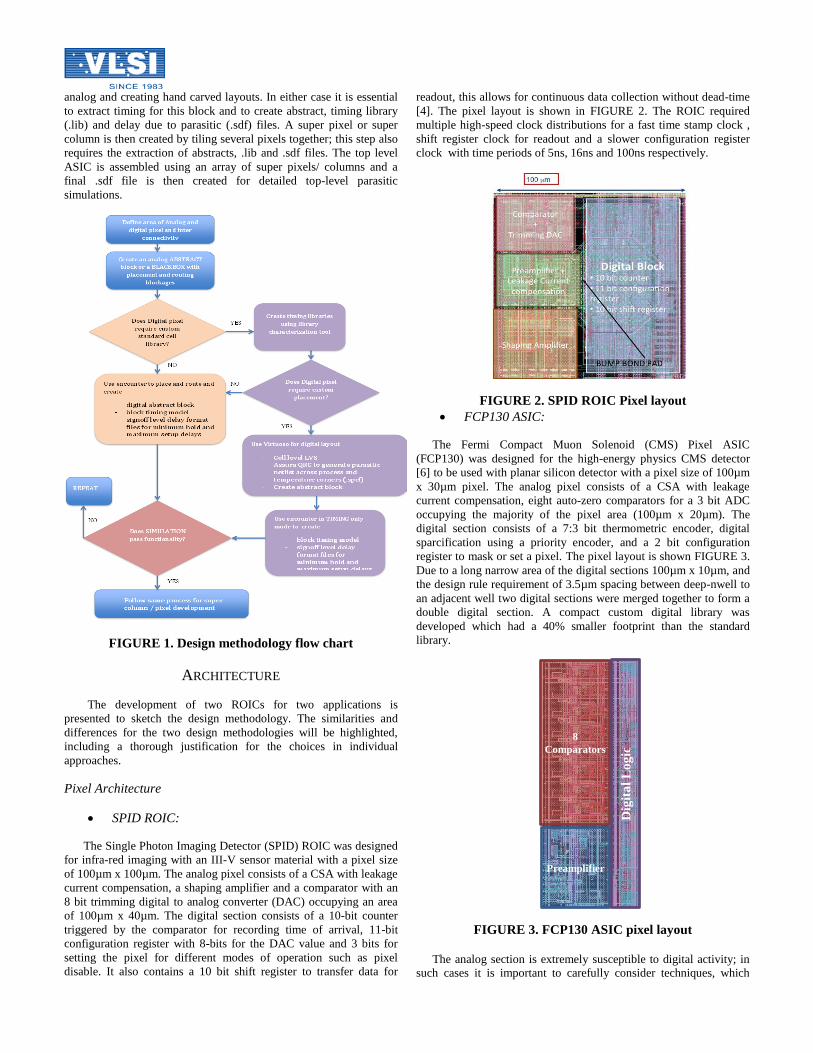
FCP130 ASIC:
The Fermi Compact Muon Solenoid (CMS) Pixel ASIC
(FCP130) was designed for the high-energy physics CMS detector
[6] to be used with planar silicon detector with a pixel size of 100µm
x 30µm pixel. The analog pixel consists of a CSA with leakage
current compensation, eight auto-zero comparators for a 3 bit ADC
occupying the majority of the pixel area (100µm x 20µm). The
digital section consists of a 7:3 bit thermometric encoder, digital
sparcification using a priority encoder, and a 2 bit configuration
register to mask or set a pixel. The pixel layout is shown FIGURE 3.
Due to a long narrow area of the digital sections 100µm x 10µm, and
the design rule requirement of 3.5µm spacing between deep-nwell to
an adjacent well two digital sections were merged together to form a
double digital section. A compact custom digital library was
developed which had a 40% smaller footprint than the standard
library.
FIGURE 3. FCP130 ASIC pixel layout
The analog section is extremely susceptible to digital activity; in
such cases it is important to carefully consider techniques, which
Preamplifier
8
Comparators
Dig
ita
l L
og
ic

would minimize noise pickup. The technology used for the ASIC
development, Global Foundaries 130nm, 1.5V LP CMOS process
provided a deep nwell, which allowed segregation between the
analog and digital function. For both the designs, the entire digital
logic was placed in deep nwell and parts of the analog function were
placed in their own deep nwell.
Super Column / Super Pixel Architecture
Creating a larger super pixel or a super column is an essential
intermediate step, particularly if it is important to avoid routing of
high-speed digital data and clocks on sensitive analog blocks. When
the analog functionality is dominant in a pixel as well as when
peripheral logic corresponds to a particular group of pixels, a super
column is a more prudent choice. On the other hand, when the digital
logic is dominant in the pixel, the choice of a super pixel with analog
islands is generally more appropriate.
SPID ROIC – Super Pixel:
The SPID ROIC top level consists of an array of 32 x 32 pixels. The
super pixel consists of 16x1 array of analog and digital sections
occupying an area of 1590µm x 90µm. Therefore the top-level ROIC
would contain an array of 2 x 32 super pixels. A routing and
placement channel of 10µm is created around each super pixel as
shown in FIGURE 4. No analog signals are present in the routing
channels; peripheral analog biasing is provided both at the top and
bottom of the ROIC matrix. This method allows the distribution of
the fast clock across the super pixel with a delay of <50ps and an
overall jitter across the chip of < 200ps. The next version of the
ROIC will use a local oscillator per super pixel to increase the fast
clock speed of up to 1GHz while still maintaining a low clock jitter.
FIGURE 4. Super pixels with routing channels
FCP130 ASIC – Super Column:
The FCP130 ASIC top-level consists of a 48 x 160 array of pixels.
The super column consisting of an array of 48x4 pixels is arranged in
the format shown in FIGURE 5, occupying an area of 4800 um x 120
um. The super column also consists of peripheral data readout
blocks. The layout is tapered from 120um to 90um to allow top level
digital routing, clock buffering and placement of additional
functionality. The top-level ASIC contains an array of 1 x 40 super
columns. The ASIC requires high-speed clock of 25ns time period
(BXClk) distributed to each pixel. The measured delay of the BXClk
across the super column is 200ps.
FIGURE 5 . A Super Column with tapered structure at
the end of the column to compensate for the lack of
routing channels
FIGURE 6 shows an alternate approach for a super pixel where
analog functionality is maintained in islands surrounded by digital
functions. This is especially useful where the percentage of the
analog layout in a pixel is low, approximately < 30% and requires a
larger array of super pixels.
FIGURE 6. Super pixels with a majority digital occupancy
ASIC Architecture
Super pixels/columns were placed together to create the top-level
array as shown in FIGURE 7. The layout at this stage includes all
other peripheral blocks as well. Non-default routing specifications
need to be defined for analog routing to pins. Top two metal layers (7
and 8) are reserved for analog power and ground routing; it is also
required for bump-bond pads. Metal 6 is used for shielding the
bump-bond pad from the digital switching noise coupling into the
CSA input. Digital power and ground is supplied from Metal 5.
A1 D1
A16 D16 D1 D2 D D D D
A1 A2 A A A A
A3 A4 A A A A
D3 D4 D D D D
D D D D D D
A A A A A A
A A A A A A
D D D D D D
D D D D D D
A A A A A A
A A A A A A
D D D D D D
Routing
Channel
s

Metal 1-4 are used for routing signals. This ensured adequate power
planning and avoiding IR drops across the ASIC.
FIGURE 7. ASIC Top level layout
TIMING ANALYSIS
Timing for compact custom hand-crafted digital blocks
Generating timing for custom hand-crafted digital cells
requires the development of a timing library with the use of the
Encounter Library characterization (ELC) tool (Cadence now
recommends using ALTOS, which is a newer version of this tool).
The digital pixel needs to pass cell level layout vs. schematic (LVS)
check followed by a detailed parasitic .spef file generation at various
temperature and process corners using the Assura QRC tool. This
then becomes the input EDI in timing mode, used to generate timing
libraries (.lib) and standard delay format (sdf) files for further
assembly and verification simulations.
Clock distribution and buffer tree synthesis
The SPID ROIC required the distribution of multiple relatively
fast clocks without the use of an on-chip phase lock loop (PLL) as
well as reset signals to various digital sections within each pixel. EDI
uses a fan-out radiating from the center of a chip to the periphery so
as to equalize the delay across the chip, it is therefore important to
create adequate routing channels to minimize jitter across the ROIC.
SIMULATION
The functional verification can be performed using the .sdf
files created by EDI. This step is critical for the iterative flow of the
design. The analog function is partially modeled in Verilog by
forcing the digital input to“1” at a well defined time, to emulate the
comparator output. The user has control over the definition of this
time, which is extracted for the best-case and worst-case analog
performance. The time definition model can be as simple as a single
value or can be more complicated to include several values which are
a result of different sources of jitter including but not limited to the
detector shot noise, analog front-end noise across temperature,
process and mismatch corners. These simulations can be repeated
several times to verify functionality.
FCP130 top-level parasitic simulations took approximately 10
minutes for each case scenario. These were primarily used to verify
data transfer from a pixel to the output pad. Based on these
simulation results the routing for the digital section of the super
column had to be changed to reduce parasitics between metal tracks
for address buses.
REQUIREMENTS
Primary requirement for this process includes the tool
interoperability setup between Cadence Virtuoso and Cadence EDI,
especially to avoid design rule violations (DRC) between analog and
digital sections. Additionally the process design kit (PDK) needs to
be tailored for open access flow.
SUMMARY
The design methodology of two pixel detector ASICs for two
diverse applications was discussed. It proposes the modification of
the standard approach and uses an iterative design flow, which needs
to be adapted based on the area constraints of the digital pixel and the
peripheral functionality for the ASIC. Custom digital layouts require
parasitic information to be extracted using Assura QRC and
subsequently using Encounter in timing mode to extract the timing
and delay files. Adapting the design flow of EDI primarily developed
for high-speed microprocessor layouts, allows the designer of pixel
detector ASICs to distribute high-speed clocks with low jitter across
a large array.
ACKNOWLEDGEMENT
SPID ROIC development was sponsored by DARPA. FCP130 ASIC
development was sponsored by DOE generic R & D detector
development funds. Fermilab is operated by Fermi Research
Alliance, LLC under contract No. DE-AC02-07CH11359 with the
U.S. Department of Energy.
REFERENCES
[1] G. F. Knoll: "Radiation detection and measurements", (3rd edn), Wiley, New York, 2007.
[2] S. M. Sze: "Semiconductor devices - physics and technology." 2nd edn, Wiley, New York, 2000.
[3] P. Fischer, et al.: "Design consideration for pixel readout chip." Nucl. Instr. Meth. A vol. 501, 2003, p. 175–182.
[4] F. Fahim, H.Mohseni, “Pixellated readout IC for single photon infrared detector for fast time of arrival applications ”, submitted to International Circuits and Systems Conference (2015)
[5] F. Fahim, D.Christian, G.Deptuch, J.Hoff, A.Shenai, M.Trimpl, T.Zimmerman, “Fermi CMS Pixel (FCP130) ASIC”, Conference proceedings for Nuclear Science Symposim (2014) – accepted