Embed Size (px)
Citation preview

Carnegie Mellon
Design for Manufacturability inVia Programmable Gate Arrays
Vyacheslav
2003
Rovner
Advisor: Prof. Pileggi/Strojwas
,~t~ Electrical & ComputerENGINEERING

CARNEGIE MELLON UNIVERSITY
Design for Manufacturability inVia Programmable Gate Arrays
by
Vyacheslav V. Rovner
A Technical ReportSubmitted to the Graduate School
In Partial Fulfillment of the RequirementsFor the Degree of
Master of ScienceIn
Electrical and Computer Engineering
Pittsburgh 15213
May 2003

Abstract
In the fast-paced semiconductor industry, time to market means everything.
Accommodating the shortened design cycles, however, is hampered by the ever-increasing design
complexity. In addition, the continual drive to achieve higher performance (speed, area, power)
has fueled the introduction of new manufacturing processes. Existing integrated circuit design
methodologies, such as standard-cells designs are failing to cope with these conflicting
requirements at a cost that is supported by ASIC product volumes. This report introduces a new
regular logic fabric, Via Programmable Gate Arrays (VPGAs). By employing a regular structure,
the design cycles can be greatly reduced. Moreover, as the technology dimensions continue
scaling downward, the product yield at the ramp-up becomes a function of systematic faults. In
order to meet the market demands, the new designs will have to focus on the Manufacturability in
addition to the performance specifications. This report presents an overview and design
corrections for the common failure mechanisms in modem Cu Integrated Circuit processes.
Furthermore, an implementation of the CLB with a manufacturability focus is described.
2
Table of Contents
TABLE OF CONTENTS ....................................................................................................... 3LIST OF FIGURES .............................................................................................................. 4LIST OF TABLES ............................................................................................................... 5
1.1 Application Specific 1Cs .................................................................................. 81.2 Field Programmable Gate Arrays .................................................................. 91.3 eASIC ........................................................................................................... 101.4 Via Programmable Gate Arrays ................................................................... 11
1.4.1 Configurable Logic Block ..................................................................... 121.4.2 Routing Architecture ............................................................................. 12
1.4 Goal .............................................................................................................. 14
2.1 Characterizing Layout Sensitivity ................................................................. 162.2 Driving Layout Optimization ........................................................................ 18
3. LAYOUT MANUFACTURABILITY OPTIMIZATION ..................................................... 193.13.23.33.43.53.63.73.8
Constant pitch of Polysilicon layer ............................................................... 19Extension of polysilicon beyond active (MOSFET end-cap) ....................... 20Width of polysilicon on field oxide ................................................................ 22Avoiding Phase conflicts ............................................................................... 23Contact redundancy ...................................................................................... 25Via redundancy ............................................................................................. 26Metal borders around vias ............................................................................ 27Via stacks ...................................................................................................... 28
MANUFACTURABILITY OPTIMIZATION OF VPGA’s ............................................... 294.1 Configurable Logic Block ............................................................................. 29
4.1.1 Look-Up Table ...................................................................................... 304.1.2 NAND Gate .......................................................................................... 324.1.3 Scan-chain DFF .................................................................................... 334.1.4 Buffers ................................................................................................... 34
5. CONCLUSIONS AND FUTURE WORK ....................................................................... 35
6. ACKNOWLEDGEMENTS ........................................................................................... 35
7. REFERENCES .......................................................................................................... 37
3

List of Figures
FIGURE 1: SHRINKING PRODUCT WINDOWS ............................................................................. 6FIGURE 2: PROGRAMMABILITY OF VPGA .......................................................................... 11
FIGURE 3: CLOSE-UP OF CROSSBAR ROUTING STRUCTURE ...................................................... 13FIGURE 4: CLOSE-UP OF SWITCHgOX ROUTING STRUCTURE .................................................... 13FIGURE 5: CHANGING TRENDS IN DEEP SUB-MICRON (DSM) TECHNOLOGY ............................. 15FIGURE 6: CONSTANT PITCH OF POLy LAYER ......................................................................... 19FIGURE 7: OVER-ETCH OF THE END-CAP ................................................................................ 20
FIGURE 8: POLY EXTENSION HELPS WITH OVER-ETCH ............................................................. 21FIGURE 9: POLY WIDTH OVER FIELD OXIDE ............................................................................ 22FIGURE 10: PHASE SHIFT MASK ............................................................................................ 23FIGURE 11:
FIGURE 12:FIGURE 13:
FIGURE 14:
FIGURE 15:
FIGURE 16:FIGURE 17:
FIGURE 18:
FIGURE 19:
FIGURE 20:
FIGURE 21:FIGURE 22:
FIGURE 23:
FIGURE 24:
FIGURE 25:
PHASE CONFLICT ............................................................................................... 24REDUNDANT ACTIVE CONTACT (POWER RAIL) ...................................................... 25
REDUNDANT ACTIVE CONTACT (CRITICAL NET) .................................................... 25
REDUNDANT CONTACT ....................................................................................... 26
REDUNDANT CONTACT (LOW LEAKAGE) .............................................................. 26GENEROUS METAL BORDERS AROUND VIA 1 ......................................................... 27
A VIA STACK ..................................................................................................... 28
CAREFUL PLACEMENT OF VIA 1 ELIMINATES VIA 1-VIA2 STACKS ............................ 28
IMPLEMENTATION OF SINGLE LUT CLB .............................................................. 29IMPLEMENTATION OF DUAL LUT CLB ................................................................ 29SCHEMATIC OF THE 3-INPUT LUT ........................................................................ 30LAYOUT OF 3-INPUT LUT ................................................................................... 31
NAND3 GATE OPTIMIZED FOR MANUFACTURABILITY .......................................... 32LAYOUT OF SCAN-CHAIN DFF ............................................................................. 33
REGENERATION B UFFER ..................................................................................... 34
4

List of Tables
TABLE 1: YIELD VS. AREA TRADEOFFS ................................................................................. 34
5

1. Introduction
The semiconductor industry has seen an exploding growth over the last decade, as the
demand for smaller and smarter devices been increasing. The observation made by Gordon
Moore in 1965 predicted exponential growth in the number of transistors on an IC [ 1]. "Moore’s
Law", as it came to be known, has become a self-fulfilling prophecy as the industry continued to
race with the introduction of new technologies. Stringent market conditions, decreasing feature
sizes, and the sheer number of devices that need to be packed onto a single IC has created an
array of unresolved issues. While the answers are not all clear, it is apparent that in order to
successfully cope with these arising problems, a different way of thinking and new methodologies
must evolve.
The driving force behind the fast paced semiconductor industry is the shortened product
lives and small product windows. As can be seen from Figure 1 it took approximately twelve
years to sell one million television sets, while taking only three days to sell the same number of
PlayStation-2 game consoles (PS-2). The gruesome market conditions reduce product’s time
[pc
3 D~4OMontl~ 3Years 5 Years 12 Y~rs
Figure 1: Shrinking Product Windows [2]
6

market, therefore requiring a shorter design cycles. In turn, a short design cycle means less time
for design verifications, and very little chance for design iterations. The possibility of something
going wrong continues to increase as the design complexity grows. In fact, currently half of
current VLSI IC designs require at least two silicon runs before arriving at a functional circuit [2].
However, if the trend pictured in Figure 1 is to continue, the reduction in time to market will
require functioning silicon after a single manufacturing run.
The short time to market is also changing the trends in introduction of new IC fabrication
technologies. In the past, the process ramp-up was separated from the volume product
manufacturing. Thus, volume production would begin only after the majority of process kinks
have been resolved. Since the systematic faults have been resolved, the yield of the product was
limited to random defects due to contamination particles. However, the market conditions
required to meet the demand depicted in Figure 1 do no allow the same luxury. To ensure the
product window will not be missed, the volume production of the product must start while the
process is still in the infancy stage. In addition, the shrinking dimensions and new materials in the
future technology nodes require higher manufacturing efficiency and tighter tolerances [2]. While
the process ramp-up must happen quickly to achieve acceptable yields, the manufacturing
realities expected in the future process makes this step costly and difficult. Yet the yield governs
the ability to meet the product demand, as well as establish the profit margins.
The current market conditions desire high performance ICs with short time to market, fast
and cheap development cycles, and high product yields. However, the current design
methodologies are not able to offer all of the needed benefits. The sections which follow will
present the design methodologies currently employed in the industry (ASIC and FPGA, and
eASIC). A new design methodology which fills the gap between ASICs and FPGAs, is
introduced which stresses more regularity and structure like an FPGA, but targets performance
and area/power of an ASIC. Finally, the remainder of this report focuses on layout optimizations
7

to cope with yield loss observed in world-class semiconductor manufacturing processes by
presenting the implementation details of the new design methodology.
1.1 Application Specific ICs
During the early stages of VLSI design, the design methodology was moving towards
designing IC for a particular application instead of using standard parts for final assembly [3].
However, with the exploding increase in circuit and process complexity, and thus the design and
manufacturing cost, few products have sufficient volume to justify the time commitment and cost
of fully custom circuit design [3]. Today’s ASIC designs may contain tens of million transistors,
and include embedded SRAMs, IP cores, as well as custom glue logic. In order to keep the design
complexity manageable, a semi-custom design methodology based on standard cells has emerged.
Currently, the standard-cell application specific integrated circuits (ASICs) represent the most
common VLSI IC design methodology.
The standard cell ASIC methodology is based on the ability to generate a library of logic-
gate cells. The library may contain several hundred physical implementations of cells, such as
logic gates with various numbers of inputs, flip-flops, and latches. In addition, the library
generally contains cells with various performance, power, and area tradeoffs. The regularity of
standard cell designs is achieved by requiring a standard "cell height" for all the cells in the
library. The resulting library is characterized for various parameters, such as timing, power, area,
etc, to be used in the standard-cell ASIC design flow. The design flow begins with a high-level
synthesizable description using any of the available hardware description languages (e.g. Verilog
or VHDL). The design is then synthesized, and mapped onto the library developed earlier. An
array of various other tools is needed to place and route the design, as well as run the needed
verification steps. This just describes an overview of the flow and hides numerous details that
make this an expensive and time-consuming process.

The standard-cell ASIC design flow has been successful for many years because of the
ability to optimize it for performance, power, or area. However, the increased design complexity
and new challenges encountered during manufacturing are increasing the cost associated with this
methodology. For example, numerous re-spin cycles may be required to obtain a functional
circuit. As the mask costs continue to increase (reaching millions of dollars for current
technology nodes) and time to market continues to decrease, the re-spin cycles become
prohibitively expensive in both time and price [4]. In addition, current market conditions may
require an existing design to be manufactured at a newer technology node (for improved
performance), or at a different fab (to increase capacity). However, the existing ASIC designs
cannot be easily retargeted for a different fab or the future technology node. In fact, such a
change may require a complete redesign, and would only be available to products with the highest
volumes.
The existing ASIC methodology offered numerous benefits in the previous years. The
industry has long enjoyed the low cost of ASIC designs. Such costs far outweighed the
development cost for high volume products. In the future, however, the costs associated with
ASIC designs will become less affordable. In order to keep new technologies affordable, more
regular design methodologies must be used [4].
1.2 Field Programmable Gate Arrays
As mentioned in the previous section, the non-recoverable engineering (NRE) costs of
ASIC methodology are unattractive for low volume products. For such products field
programmable gate array offer a significant cost advantage [4]. The FPGA architecture is
characterized by low upfront costs, since the costs associated with the design and manufacturing
of the FPGA can be amortized over numerous products [3]. In addition, the FPGA offers fast time
to market, and due to its field programmability, practically free re-spin cycles. The fast time to
9

market is achieved through highly regular structure, which simplifies clock and power
distribution [5]. Moreover, unlike an ASIC, an FPGA has the ability for any signal to become
observable, which can facilitate product debugging. In fact, this makes FPGA platform optimal
for initial product development. Furthermore, the FPGA designs can be easily ported from one
technology to another, requiring only a simple re-synthesis step to retarget the design to a newer
(or even different) family of FPGAs. It should be noted that 100% yields could be achieved for
FPGA products, something that is unheard of in the ASIC designs. This is due to the re-
programmability of the device, allowing the damaged sections of the FPGA to be avoided during
programming. However, the benefits of the architecture come with significant penalties [4].
The field programmability in an FPGA is achieved through the usage of SRAM cells in
programmable logic blocks and interconnects. The additional SRAM cells waste valuable silicon
resources, thereby responsible for up to ten-fold circuit area increase as compared to an ASIC
design [3]. In addition, since the delay through the circuit is governed by wire delay, the usage of
programmable interconnect can substantially affect the wiring delays [3] [5]. Consequently, the
numerous advantages offered by the FPGA cannot be used by designs requiring high
performance, small footprints, and low power consumption.
1.3 eASIC
It is apparent that there is a wide design space gap between the ASIC and FPGA
methodologies [4][6]. One of the commercial design methodologies, which attempt to fill void, is
the technology from eASIC. Just like an FPGA, eASIC is regular structure consisting of field
programmable logic blocks. Given that the major performance penalties in the FPGA were
attributed to field programmable interconnect, eASIC eliminated the field programmability;
instead, the interconnect of the resulting fabric is mask programmable using metal and via masks.
The eASIC fabric offers performance, area, and power comparable to an ASIC design [6]. At the
10

same time, the design can take advantage of the benefits of FPGA methodology, such as regular
clock trees and power grid. The design methodology claims that re-programmable logic can be
used for logic edits and debugging [6]. However, the extent of logic corrections is significantly
limited by the fixed interconnects. Additionally, debugging of the design is restricted by the mask
customization as some nets become unobservable.
1.4 Via Programmable Gate Arrays
The via programmable gate array fabric [3][4], just like eASIC, fills the void between the
ASIC and FPGA methodologies. The goal of the proposed fabric is to combine the favorable
features of the ASIC and FPGA methodologies. As noted previously, architecture regularity
becomes a requirement as the complexity of the design increases. In addition, the new
architecture must have performance and per part cost comparable to an ASIC design, while
having short design cycles, low design costs, and high yields analogous with FPGA architectures.
The VPGA architecture employs regularity in customizable logic blocks as well as the
interconnect. The extreme regularity of the fabric will improve the manufacturability and
Connection m/e Con~ection not made
zon
Figure 2: Programmability of VPGA [8]
Un~d~erlayed Si ’ con
predictability of the design [3][4][5]. The customization of the logic blocks, as well as the
interconnect is performed by customization of vias instead of SRAM controlled pass gates. If a
11

connection is needed between two interconnect levels, the via mask layer would contain a hole in
the chrome for the location of the via, resulting in metallization pictured on the left of Figure 2.
However, if a connection is not required, the chrome on the via mask will be present. Thus, the
location would be filled with the dielectric, resulting in picture on the right of Figure 2.
Given that SRAM controlled pass gates have been replaced with vias, the performance
penalty due to the interconnect should be comparable to that of an ASIC design. In addition, just
like the interconnect, the logic blocks of the VPGA are configured using a via mask. Thus, the
area of VPGA cell would be significantly lower than a comparable eASIC or FPGA cell. One of
the other immense benefits of VPGA architecture is the ability to keep low design costs (NRE
costs). This is possible because the design methodology requires only small number of masks,
specifically via masks, for application-specific customization, in contrast to a standard cell ASIC
which requires a full set of masks (ranging between 26 and 32 different masks).
1.4.1 Configurable Logic Block
The configurable logic block (CLB) is the building block of the VPGA fabric. This block
contains a via programmable look-up table (LUT), a scan chain D flip flop, NAND gates, and
inverter/buffer pairs. As can be noticed from the contents of the CLB, the VPGA architecture has
adopted a heterogeneous logic block. The studies of heterogeneous CLBs have shown a
significant speed improvement, as the synthesis tool is able to swap in the faster NAND for the
LUTs [7]. In addition, the structure and the size of the LUT have to be properly selected for
superior performance and efficient utilization of silicon area. Further discussion on the selection
of LUT topologies and sizes used in the VPGA architecture can be found in [5] and [8].
1.4.2 Routing Architecture
Since the interconnect contributes the most to the delay in current semiconductor
processes, efficient routing architecture must be used in the VPGA. Primarily, there are two
12

choices for the interconnect: crossbar and switchbox routing. The precise choice of the routing
architecture is beyond the scope of this report, and is addressed in [5]. In fact, both routing
approaches may be needed in the final VPGA methodology. The crossbar and switchbox
structures are shown in Figure 3 and Figure 4, respectively. Each structure offers its benefits and
drawbacks. For example, the crossbar structure allows for complete interconnectivity between
any numbers of tracks, while the switchbox structure is limited in the number of tracks that can be
connected. On the other hand, the crossbar tracks are often made longer than required,
introducing extra capacitance, and thus delay into the circuit.
Figure 3: Close-up of crossbar routing structure
Figure 4: Close-up of switchbox routing structure
13

1.4 Goal
This report presents the physical implementation of the configurable logic block (CLB)
a commercial 0.13#m Cu process. Furthermore, the physical implementation focuses on
manufacturability of the CLB, and suggests design optimizations needed to achieve a higher
yielding circuit (in terms of all of the layers up to metal 2). The next section focuses on the flow
that can be used to analyze yield losses in the deep sub-micron processes. Section 3 describes
design optimizations for most common yield loss mechanisms in the modern commercial
processes. Finally, Section 4 presents the optimized CLB for the VPGA architecture, and
conclusions and future work are discussed in Section 5.
14

2. Manufacturability
As the devices continue to scale down into sub-100nm dimensions in order to keep pace
with the Moore’s Law, the difficulties in the future technology nodes are becoming surreal. For
example, the optical lithography is being pushed to its fundamental resolution limit, requiring
numerous resolution enhancement techniques (RETs) to achieve adequate pattern fidelity [9].
Therefore, radical changes will be required in the design methodology to keep up with new
manufacturing realities.
The yield loss mechanisms in an IC can be placed into one of three categories: process
related yield losses, systematic effects, and random defects [ 10]. Misprocessing, such as some
kind of equipment malfunction, causes the process-related yield losses. The systematic effects are
due alignment or printability problems, while the random defects are caused by foreign particles
I00o/o -
90%
70% - --B-- Tradit ion al defect-I im it ed yield
~ Feature-limited yield60%
0.8pm O~Spm 0.35 prn 0,25 pm 0.18 IJm 0.13 pm 0.1pm
T echnol ogy Node
Note" Feeture-li ml:ed yteld esa umes t he feeture ~ailure ra~ Im/:r o~s by approximate~y SO% eech
Figure 5: Changing trends in deep sub-micron (DSM) technology [2]
and contamination of the wafer. In earlier technology nodes, yield loss was a simple function of
the defect density and the die area, thus random defects were the dominant yield loss mechanism
15

[10]. However, as Figure 5 suggests, a different trend is emerging in deep sub-micron (DSM)
technologies. In fact, feature limited yield, systematic in nature, was already dominating the
defect limited yield in the 0.18#m process. Further dimension scaling will continue to see the
trend, with technologies in sub 100nm regions becoming a solely a function of feature limited
yield.
When random defects dominated the yield loss, the traditional methodology to design for
maximum yield required continued shrinkage of layout. In an effort to reduce the area, smaller
standard and SRAM cell sizes were continually introduced [ 10]. However, with an emergence of
different trends in yield loss mechanisms, the traditional approach can no longer work. In fact,
product yield presently depends more on the design attributes than the physical chip area
[10][ 11]. Therefore, the yield optimization must focus on optimizing critical features such as
contacts, vias, poly end-caps, and etc. However, in order to accurately guide the yield
optimization step, the interactions between product design attributes and manufacturing process
have to be accurately understood [9] [ 10]. Specifically, the amount of yield loss attributed to each
defect type is absolutely necessary in any attempt at improving yield [12].
2.1 Characterizing Layout Sensitivity
There are three necessary steps to quantify the defect induced yield losses. First the
defects present in the process must be detected and categorized. In parallel, the physical design of
the product is analyzed to establish the number of potential defects, the so called "killer defects",
that can cause product failures. Finally, the failure rates from process characterization are
combined with the number of potential defects to obtain the product yield [ 10] [ 12].
One of the methods available for detecting and characterizing defects in the VLSI
manufacturing involves the fabrication of test vehicles. Such a characterization chip is designed
16

to quantify and highlight prevalent failure mechanisms present in the process [ 12] [ 13]. There are
several other methods available for detecting and characterizing defects in the VLSI
manufacturing process. For example, an optical inline inspection method can be utilized. Each
defect detection system has its own advantages and drawbacks, which are further discussed in
[12]. It is possible to obtain defect density of the process for a specific defect type by analyzing
the vast amounts of data obtained from the characterization vehicles. The methods for data
analysis are beyond the scope of this work, and are further described in the literature, such as [12]
and [ 13].
The second step in quantifying defect induced yield losses requires an analysis of product
design. The physical design is analyzed for sensitivity to possible defects. For example, in order
to determine the sensitivity of the design to shorts or opens, critical area computations must be
made for possible defect sizes. The concept of critical areas dates back to 1966 when P.W. Cook
observed that the areas affected by the defects depended on defect size [11]. The critical area was
defined as the area in which the center of a defect must land in order to cause a circuit failure
[11]. For defects not dependent on area, such as defects dealing with via or contact opens, a
simple counting is performed to determine the number of features susceptible for failures
[ 10][ 12]. For example, a count of single active contacts would result in the number of features in
the design susceptible to active contact opens.
By using the failure rates obtained from process characterization and the appropriate
critical area/counts from product analysis, it is possible to attribute the yield loss due to the
potential defect types [10][12]. If the defect induced yield losses analyzed are independent, the
overall yield of the product can be computed by multiplying the individual yield losses [ 10]. As
described in the next section, by using the yield loss information, the product layout can be
modified to reduce its sensitivity to the defects.
17

2.2 Driving Layout Optimization
To achieve significant impact on yield, layout optimization should be performed after the
analysis described in the previous section is complete. Once, the product failure rates for
individual defect types are obtained, the priority of optimization of layout features becomes
apparent. Specifically, the features causing the highest yield loss should be optimized first. In
addition, the yield loss can dictate the allowed tradeoffs between defect types in order to
maximize yield. This kind of new approach to yield optimizations will be required in the new
feature-limited technology nodes.
18

3. Layout Manufacturability Optimization
Current manufacturing processes has gotten very complicated. Numerous design rules
have been introduced in order achieve economical yields. The following sections discuss
common failure mechanisms (poly CD variation, line-end shortening, cracked salicide, open
contacts and vias, and mask misalignment), as well new manufacturing techniques (alternating
Phase Shift Masks). In addition, layout optimizations are proposed to cope with the failure
mechanisms, and extract the benefits of new manufacturing techniques.
3.1 Constant pitch of Polysilicon layer
Accurate fabrication of the polysilicon layer is one of the most important steps in today’s
processes. The poly layer determines the channel length of MOSFETs, and thus determines their
electrical characteristics. Critical dimension (CD) variations of the polysilicon lines can
thought of as errors in the underlying SPICE models used during the design process. While small
variations in CD are to be expected, large changes may make the design performance fall outside
Figure 6: Constant pitch of poly layer
allowable limits. As the dimension of the devices continue to shrink, the faithful reproduction of
the poly layer becomes difficult. In fact, future technologies will see large variations in critical
dimensions for certain pitches [4].
19
Printing regular grating patterns allows for optimization of lithography process to
maximize the process window. Hence, to minimize the variation of poly linewidth, in ideal case,
poly lines should be placed over active regions at a constant pitch (Figure 6) [4]. Moreover, OPC°
tends to give best results when used on uniform density patterns [4]. Designing with constant poly
pitch may become especially necessary in the future technologies, since some of pitches may
become forbidden because of their poor printability (even with OPC corrections) [4].
It is worth noting that the layout presented in Figure 6 only focuses on constant pitches
for poly lines over active regions, as this is what determines the channel length of the fabricated
transistor. The poly lines over field were not kept at constant pitch; as these will only affect the
parasitics of the poly interconnect.
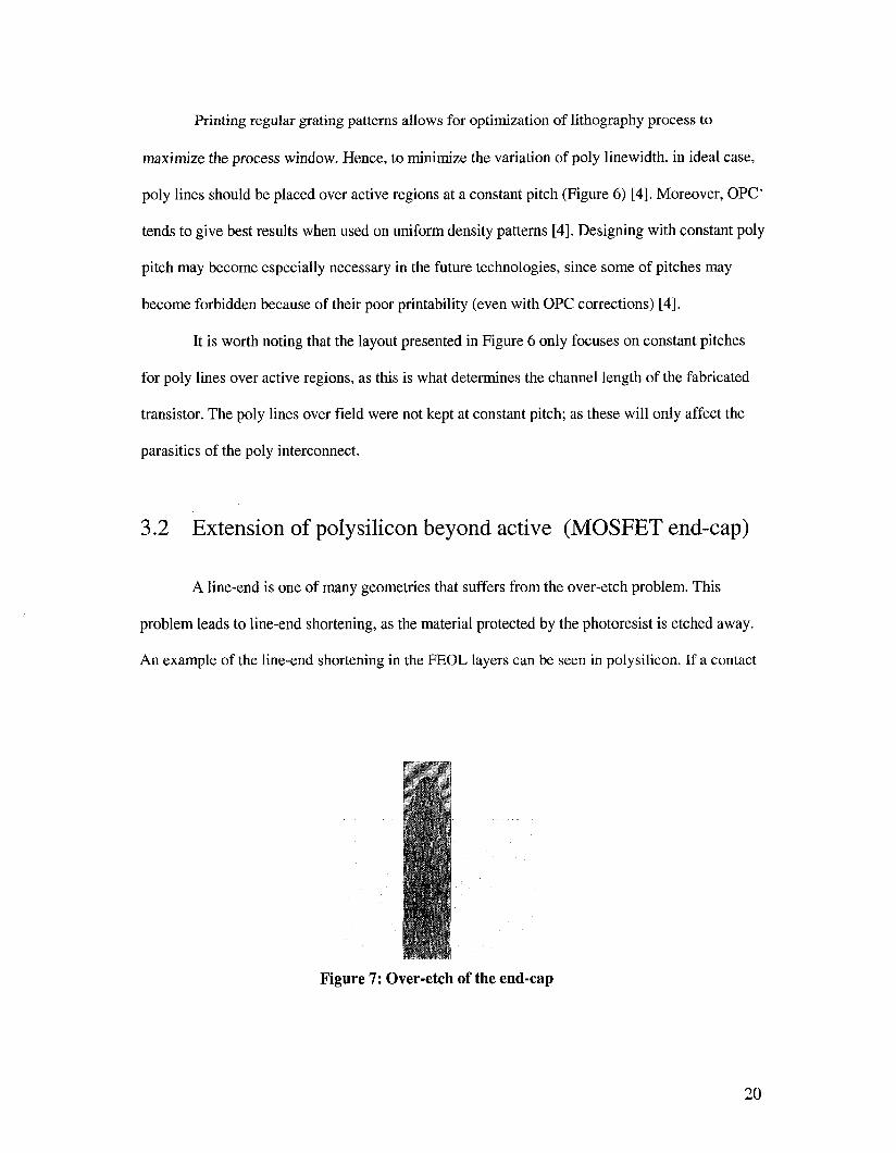
3.2 Extension of polysilicon beyond active (MOSFET end-cap)
A line-end is one of many geometries that suffers from the over-etch problem. This
problem leads to line-end shortening, as the material protected by the photoresist is etched away.
An example of the line-end shortening in the FEOL layers can be seen in polysilicon. If a contact
Figure 7: Over-etch of the end-cap
20

is present in the area that suffers from line-end shortening, the resulting connection can become
highly ohmic. This failure mechanism deals with the line-end shortening of end-caps. As can be
seen in Figure 7, the end-cap of the transistor is the short piece of poly that extends past the active
region. The darker region in Figure 7 shows an over-etch problem. The resulting MOSFET
channel can be thinner at the edge of the active region. This increases the leakage currents in the
FET. A more severe problem occurs if additional poly is etched away, as the drain the source
regions of the MOSFET can become shorted.
In addition to OPC, which can add "hammerhead" corrections to the end-cap, the poly
Figure 8: Poly extension helps with over-etch
end-cap can be extended past its design rule value by x #m, as seen in Figure 8. In order to
determine the value of x, this failure mechanism will have to be characterized for the specific
process, as previously discussed in this report. Moreover, there is a tradeoff between various
failure mechanisms; for example, the extension may increase the critical area if there are other
poly lines in the neighborhood. Thus, this extension length becomes an optimization problem
based on failure rates in the specific process.
21

3.3 Width of polysilicon on field oxide
In order to reduce the sheet resistance of the polysilicon, a thin layer of conductive
salicide is created on to which results in the poly layer sheet resistance being an order of
magnitude smaller, so it can be used for some of local interconnect. However, the process of
growing salicide on the poly layer works at different rates, depending on the doping of the
substrate below. If a polysilicon line is placed at the boundary between opposite type of dopings,
which is frequently the case, the connected segments will experience different growth rates of
salicide.
The thin layer of salicide experiences physical stresses and strain at the junction. Due to
these stresses, the salicide has a high chance of breaking or cracking. If the salicide develops such
a fault, the poly line becomes highly resistive. Since, the poly is used for local interconnect, a
highly resistive path will significantly change the RC constant, and thus timing. Thus, possibly
affecting the functionality of the circuit. In addition, poly contacts should not be placed across the
nwell:
+ 2x
Figure 9: Poly width over field oxide
n/p transition due to the same reasoning. The contacts placed on top of weak salicide, can cause it
to crack, creating a highly ohmic contact and a resistive poly path. In order to make polysilicon
more resistant to this fault, the poly line can be made wider around the n/p transition. As shown in
Figure 9, the poly is widened beyond its minimum design rule value. The poly is widened y #m
on both sides of the rdp transition as suggested by the Figure 9.
22

The extra poly area will reduce the stresses in the salicide, and prevent it from cracking.
However, the additional poly will increase the critical area of shorts between adjacent poly lines.
In the example shown in Figure 9, the space between adjacent poly lines was well above the
minimum design rule value. Thus, while the critical area is slightly increased, the change in the
number of possible shorts would remain insignificant.
3.4 Avoiding Phase conflicts
Printing features at dimensions below the exposure wavelength in deep sub-micron
technologies requires powerful resolution enhancement techniques (RET). One of such
techniques is the use of alternating Phase Shift Masks (altPSM) [14]. In fact, altPSM can
effectively double the resolution of a conventional optical lithography system. The phase shifting
Cross-section of altPSM
180° ]OO IIIIIIIIIIII I~ II
~ 180°
/chroine
Figure 10: Phase Shift Mask
mask uses destructive interference to cancel out the errors in the lithography step. To create the
destructive interference, 180° phase shift must be introduced between adjacent features. This
requires a special mask, as shown in Figure 10.
23

As can be seen from the figure, the phase shift is created by selectively etching away the
mask substrate in areas where the phase shift needs to be introduced. The exact depth a mask has
to be etched depends on source wavelength and the refractive index of the mask material [14].
The introduction of phase shifts severely limits the layout patterns that can be used. For
example, a structure displayed in Figure 11 cannot be printed using altPSM techniques. This is
due to a phase conflict. For example, if0 ° phase is used in area A, 180° phase shift must be
introduced in area B. This creates a phase conflict in area C, as any phase introduced there (0° or
180°) will conflict with one of the other areas, and not cause the destructive interference needed
for this RET. In fact, one cannot perform non-conflicting phase assignments for such a layout
pattern.
Of course, completely eliminating patterns that cause phase conflicts would be an ideal
solution. However, these patterns cannot be always avoided. When devices need to have fingers
(needed for devices with large W/L ratios), the pattern shown in Figure 11 is present. In order
Figure 11: Phase Conflict
24

print such patterns, the less critical leg of the "T" junction should be made larger. While this
doesn’t eliminate the phase conflict, a phase assignment, which allows the critical legs of the "T"
junction to be printed correctly, can now be made. Referring back to Figure 11, if the LEG X is
less critical, increasing its width allows the following phase assignment: A 0° phase shift, B 180°
phase shift, and C 180° phase shift.
3.5 Contact redundancy
A contact layer is used to connect metal layer to either poly or source/drain regions. A
failed contact would mean an open or highly ohmic connection to the devices on silicon. While,
the number of failed contacts depends on the quality of the process, introducing contact
redundancy can reduce the number of failed connections. Adding contact redundancy becomes a
tradeoff between other failure mechanisms, area, timing, and power consumption.
In order to add a redundant contact, the existing polysilicon, active, and metal I region
may have to be expanded. By expanding these layers, the parasitic properties of interconnect and
the devices will change. For example, expanding the active region will increase the source/drain
capacitance of the transistor, while reducing the contact resistance to the region. Similar behavior
Figure 12: Redundant active contact(power rail)
ch in activeii area to reduce:apacitance
Figure 13: Redundant activecontact (critical net)
25

would be observed for requirements needed to introduce redundancy in polysilicon contacts.
For example, Figure 12 shows a power (grid) connection to an active region of an NMOStransistor. By introducing the redundant contact, the active region had to be expanded. This inturn increases the capacitance at the node. However, this is a connection to a power rail. Extracapacitance on this net is actually helpful, as it will filter the noise present in the power line.
Figure 13 shows an output node of a three input NAND gate. Extra diffusion capacitance
Figure 14: Redundant contact Figure 15: Redundant
(high leakage) contact (low leakage)
at this node will affect the timing of the gate, and may not be appropriate if the gate fails to meet
its timing requirements. It may be useful to note the notch in the active region was designed to
reduce the capacitance at the output node. When making connections to transistors with small
W/L ratios, it is tempting to introduce redundancy as shown in Figure 14. However, the sharp
active region comer introduces strains in the polysilicon layer, and increases leakage currents.
Thus, if area permits, a scheme shown in Figure 15 should be followed for introducing
redundancy in transistors with small W/L ratios.
3.6 Via redundancy
The concept behind adding via redundancy is not too different from the contact
redundancy described in earlier section. However, the VPGA architecture, being based solely on
26

mask programmable vias warrants special consideration. In the current architecture only vial
mask is not programmable. The higher via layers all have programmability. Since the positions of
vial are known, the redundancy can be added to this layer to improve the manufacturability.
However, adding via redundancy to higher layers comes with a high area penalty, because the
actual location of the vias are unknown, and redundancy must be added to all "potential via"
locations. Therefore, improving manufacturability of upper via layers will have to be done
through generous metal extensions and elimination of via stacks (both are described in future
sections).
3.7 Metal borders around vias
Slight mask misalignment occurs during the manufacturing process. If the via mask is
misaligned far enough, there may be an insufficient metal coverage under the new location of the
via. This failure will create a higher than normal via resistance. In addition, the lithography and
etch step cause line-end shortening around the end of metal runners. Thus, placing vias at the end
of a long metal runners becomes problematic, as these arrangements can cause highly resistive
connections due to limited metal coverage under the via.
The design rules require only minimum borders around the vias. Usually the requirement
is for two sides of the via (preferably opposite) to have borders. The addition of metal borders
Figure 16: Generous metal borders around vial
27

all four sides will decrease the failure rates of vias due to mask misalignment and line-end
shortening of metal runners. Figure 16 shows generous metal extensions on all four sides of the
via (the extra long extension on one of the sides is needed due a contact on a lower layer).
3.8 Via stacks
The reasons behind stack failures in Cu processes are still being carefully studied. It is
not quite clear if the higher failure rates of stacked vias are caused by mask misalignment or if
there is some interaction between the stacked vias. A cross-section of via stack is shown in Figure
18. Since via stacks tend to experience higher failure rates, removing via stacks is one of the
effective ways to improve the manufacturability in the BEOL layers. Moreover, via redundancy
can only be introduced at vial in the VPGA fabric, making elimination of via stacks critical to
BEOL yield.
The CLBs making up the VPGA fabric contain the locations of potential vias on a fixed
routing grid. Because the location of the final via placement is not known in advance, the only
effective way of breaking up via stacks is to place vial off the potential via grid, as shown in
Figure 17.
Figure 18: A via stack
Potentialvias
Figure 17: Careful placement of vialeliminates vial-via2 stacks
28
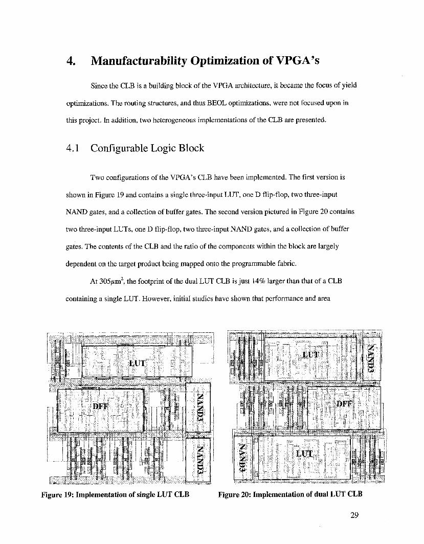
4. Manufacturability Optimization of VPGA’s
Since the CLB is a building block of the VPGA architecture, it became the focus of yield
optimizations. The routing structures, and thus BEOL optimizations, were not focused upon in
this project. In addition, two heterogeneous implementations of the CLB are presented.
4.1 Configurable Logic Block
Two configurations of the VPGA’s CLB have been implemented. The first version is
shown in Figure 19 and contains a single three-input LUT, one D flip-flop, two three-input
NAND gates, and a collection of buffer gates. The second version pictured in Figure 20 contains
two three-input LUTs, one D flip-flop, two three-input NAND gates, and a collection of buffer
gates. The contents of the CLB and the ratio of the components within the block are largely
dependent on the target product being mapped onto the programmable fabric.
At 305#m2, the footprint of the dual LUT CLB is just 14% larger than that of a CLB
containing a single LUT. However, initial studies have shown that performance and area
Figure 19: Implementation of single LUT CLB Figure 20: Implementation of dual LUT CLB
29

requirements of the circuit implemented using dual LUT CLBs is superior to the one
implemented using a single LUT CLB.~ This can only be explained by better utilization of the D
flip-flops in the CLB. But, this is not at all unexpected. For example, circuits containing highly
datapath-like components would most often contain some sort of a full adder. Two single LUT
CLBs will be required to implement a full adder, potentially wasting the one of the D flip-flops.
However, a complete full adder could be implemented using a dual LUT CLB. In addition, the
LUT inputs are independent, allowing for an efficient use of both LUTs in control circuits.
notC~
VDD
GND
Figure 21: Schematic of the 3-input LUT
4.1.1 Look-Up Table
The look-up table (LUT) design used in the CLB is built out of transmission based 2:1
muxes (refer to Figure 21). The two inputs (A and B) control select lines of the resulting 4:1
The inputs of the mux are connected to either vdd or gnd with programmable vias. Using this
notA~ ~~ ~A A--~- _~)-nOrA
arrangement, any two input function can be created. In order to create a three input function, a
third input (C), or its complement, can be connected to the input of the mux. This configuration
allows for a three input function to be realized using only two levels of transmission gate muxes,
significantly speeding up the LUT [8]. In addition, the LUT, and the input buffers must be
carefully sized in order to achieve acceptable performance.
~ Veerbhan Kheterpal performed the initial assessment.
30

The layout of the LUT was designed using a commercial 0.13#m Cu process. The layout
of the complete LUT is presented in Figure 22. The resulting layout keeps in mind the common
failure in the modern copper processes, and incorporates the fixes presented in earlier section to
achieve better manufacturability and yield. The layout of the LUT has complete redundancy in
active contacts (point A in the figure). Since poly can be used for local routing, the redundancy
poly contacts can be used to reduce the resistance of the long runners (as shown by the marker B).
Figure 22: Layout of 3-input LUT
Points C in figure show an increase in poly width to reduce the stress on the salicide. The layout
also implements longer poly end-caps (points E), and complete vial redundancy (point
In addition, the layout of the LUT helps to resolve the phase conflicts by widening the
non-critical poly lines. Marker F2 points to a poly line of a fingered device. The "H" structure
will present a phase conflict. The only non-critical line is the middle bar, which is widened. F1
shows one of the other patterns that can cause phase conflict (even/odd run). Once again, the poly
line is widened to alleviate the problem.
31

4.1.2 NAND Gate
The LUT structure described in the previous section can implement any of the two or
three input functions. Compared to simple logic gates (NAND, NOR, INVERT), the LUT wastes
area, consumes more power, and works slower. If a two-input NAND gate is allowed, inversions
at each of its inputs and its output, it can implement fourteen out of sixteen two-input functions
(XOR and XNOR cannot be implemented using a NAND gate). A three-input NAND gate with
inversions at inputs and output can implement 56 out of 255 three-input functions. However, a
Figure 23:NAND3 gate optimizedfor manufacturability
significant fraction of logic functions occurring in the designs falls into one of the 56 functions
that can be implemented by the NAND gate [7].
Figure 23 illustrates a NAND gate used in the CLB. The NAND gate was optimized for
manufacturability. The gate contains 100% redundancy of active and poly contacts, as well as
vial (placed as to not create via stacks with potential vias). In order to reduce the capacitance
the output node, the drain areas of the output transistors is minimized.
32

4.1.3 Scan-chain DFF
The flip-flop used in the configurable logic block was taken from the standard library of
the commercial 0.13/xm Cu process being used to implement the VPGA platform. The design was
significantly modified in order improve printability and yield of the cell. The resulting layout is
shown in Figure 24. The area of the original cell layout was 34.3#m2, while the layout shown
bellow has an area of 41.6/zm2. This constitutes an area increase of about 20%. The additional
Figure 24: Layout of scan-chain DFF
area was used to make the cell more resistant to the failure mechanisms described in Section 3.
Table 1 displays the data for amount of redundancy possible in active and poly contacts. By
increasing the area by 20%, the number of redundant poly contacts possible increased by over
420%, from 13.3% redundancy to 57.1% redundancy. Similarly, the number of redundant active
contacts increased by over 230%, from 25% redundancy to 59.4% redundancy.
The VPGA fabric, like an ASIC is limited by the wiring capacity. In addition, the fixed
routing structure requires a large area to successfully route the needed signals. Since the routing
structure is built on top of the CLB, the size of the CLB can increase, up to the size of the routing
33

fabric, without incurring any overall area penalty. Thus the benefit of better manufacturability
will outweigh the 20% increase in the area of DFF
Active Connections Poly Connections
Total Redundant Total Redundant
Original DFF 32 1 15 0
Modifications without area32 8 15 2increase
20 % are increase 32 19 14 8
Table 1: Yield vs. Area Tradeoffs
4.1.4 Buffers
The eight-inverter/buffer pairs are uniformly arranged in the CLB. The layout of one of
such configurations is shown in Figure 25. The inverter/buffer pairs server two purposes. The
le poly for improved~ufacturability ofered devices
Figure 25: RegenerationBuffer
inverter output provides the support for complementary inputs and outputs for the NAND gate.
This allows the NAND gate to realize 56 out of 255 three-input functions. The second output is
driven by a large MOSFET, and provides signal conditioning for long interconnect.
34
5. Conclusions and Future Work
Current research suggests that the yield loss issues will only increase for future
technology nodes [4]. This report discusses yield loss mechanisms common to modern copper
processes. Physical design optimizations have been suggested to combat the current problems as
they would occur for the proposed via programmable gate array architecture. Importantly, by
employing this highly regular logic fabric, such detailed optimization is made possible, and the
resulting VPGA architecture promises to achieve higher manufacturability and predictability [4].
A physical implementation of the configurable logic block, which is the primary building block
of the VPGA, is presented in this report. The physical implementation focuses on employing the
regularity and the design optimizations for common yield loss mechanisms to achieve a more
manufacturable design.
Since there are significant contributions to yield loss at the FEOL layers and metal 1, our
focus was on optimization of the critical layers. However, a substantial amount of yield loss can
also be attributed to the higher layers of metallization. Since the VPGA employs a regular routing
structure, the design for manufacturability methodologies should ultimately be employed for the
interconnect layers as well. A much needed study should analyze how much redundancy can be
afforded in the interconnect in order to reduce the effect of yield loss due to via opens. In
addition, a knowledge of the actual failure rates in a given fabrication process would be helpful in
guiding further optimization efforts.
6. Acknowledgements
I would like to extend my deepest thanks to my co-advisors Professors Andrzej Strojwas
and Larry Pileggi. Thank you for your continued support and advice during this project, and the
years I spent at Carnegie-Mellon University. I would also like to extend my thanks to all the
35

people with whom I worked on the VPGA project: Professor Herman Schmit, Padmini
Gopalakrishnan, Veerbhan Kheterpal, Aneesh Koorapaty, Chetan R. Patel, and Kim Yaw Tong.
Thank you for a warm welcome when I’ve joined the project, and quickly getting me up to speed.
Finally, I’d like to thank my parents for providing me with numerous opportunities, and
more importantly believing in me. This would not have been possible without you.
36

7. References
[1]
[2]
[3]
[4]
[5]
[61
[7]
[8]
G.E. Moore, "Cramming more components onto integrated circuits," Electronics,
Vol.38, No. 8, April 1965.
A.J. Strojwas, "Design Manufacturing Interface for 0.13/.tm and Bellow," Invited
Embedded Tutorial, International Conference on Computer Aided Design, San Jose, CA,
November 2000.
L. Pileggi, H. Schmit, J.Shah, Y. Tong, C. Patel, and V. Chandra, "A Via Patterned Gate
Array (VPGA)," Technical Reports Series of the CMU Center for Silicon System
Implementation, No. CSS102-15, March 2002.
L. Pileggi, H. Schmit, A.J. Strojwas, P. Gopalakrishan, V. Kheterpal, A. Koorapaty,
C. Patel, V. Rovner, and K.Y. Tong, "Exploring regular fabrics to optimize the
performance-cost trade-off," Proc. of Design Automation Conference, June 2003.
C. Patel, A. Cozzie, H. Schmit, J. Shah, Y. Tong, and V. Chandra, "An Architectural
exploration of Via Patterned Gate Arrays," Proc. of International Symposium on Physical
Design, April 2003, pp. 184-189.
eASIC Corporation, http://www.easic, corn, May 2003.
A. Koorapaty, V. Chandra, K.Y. Tong, C. Patel, L. Pileggi and H. Schmit,
"Heterogeneous programmable logic block architectures," Proc. of Design, Automation,
and Test in Europe, March 2003, pp. 1118-1119.
K.Y. Tong, V. Kheterpal, V. Rovner, L. Pileggi, H. Schmit, and R. Puri, "Regular Logic
Fabrics for a Via Patterned Gate Array (VPGA)," submitted to CICC 2003.
37

[9] L.W. Liebmann, "Layout impact of resolution enhancement techniques: impediment or
opportunity?," Proc. of International Symposium on Physical Design, April 2003, pp.
110-117.
[10] D. Ciplickas, A. Joshi, S.F. Lee, and A.J. Strojwas, "Maximize Yield Through Design:
The Yield Impact Matrix," Semiconductor International, October 2002.
[11] C.H. Stapper and R.J. Rosner, "Integrated Circuit Yield Management and Yield Analysis:
Development and Implementation," IEEE Transactions on Semiconductor
Manufacturing, Vol. 8, No. 2, May 1995, pp. 95-102.
[12] D.J. Ciplickas, X. Li, and A.J. Strojwas, "Predictive Yield Modeling of VLSIC’s,",
International Workshop on Statistical Metrology(Tech. Digest), June 2000, pp. 28-37.
[13] M. Craig, A. Jee, and P. Maniar, "An integrated approach to yield loss characterization,"
Proc. International Test Conference, 2002, pp. 350-356.
[14] F. Heng, L. Liebmann, J. Lund, "Application of Automated Design Migration to
Alternating Phase Shift Mask Design," International Symposium on Physical Design,
April 2001.
[15] K.Y. Tong, "Regular Logic Fabrics for Via Patterned Gat Arrays," MS Thesis Report,
Carnegie Mellon University, May 2003.
38


![Architecture of field-programmable gate arrays ...arantxa.ii.uam.es/~die/[Lectura FPGA Architecture] Architecture of... · Architecture of Field-Programmable Gate Arrays JONATHAN](https://img.dokumen.tips/doc/110x75/5f41b9382d13750b786f03bd/architecture-of-field-programmable-gate-arrays-dielectura-fpga-architecture.jpg)


![Field Programmable Gate Arrays [Fpga]](https://img.dokumen.tips/doc/110x75/544092dcb1af9f441d8b45c9/field-programmable-gate-arrays-fpga.jpg)


