Embed Size (px)
Citation preview

HOTCHIPS 2001
©R.A. Rutenbar, 2001 1
© R.A. Rutenbar 2001
Rob A. RutenbarCarnegie Mellon UniversityPittsburgh, PA, [email protected]://www.ece.cmu.edu/~rutenbar
Design for Leading-Edged Mixed-Signal ICsAnalog Intellectual Property:Why, When, How
© R.A. Rutenbar 2001
Be Honest: I Say Analog You Think This

HOTCHIPS 2001
©R.A. Rutenbar, 2001 2
© R.A. Rutenbar 2001
Analog--Who Really Cares?
Copyright © 1993, The National Gallery, LondonCopyright © 1993, The National Gallery, London
Copyright © 1993, The National Gallery, LondonCopyright © 1993, The National Gallery, London
-+
© R.A. Rutenbar 2001
Modern Systems Have Analog Interfaces
AnalogInterface
DigitalComputing
Core
Telecom Consumer
Automotive Medical

HOTCHIPS 2001
©R.A. Rutenbar, 2001 3
© R.A. Rutenbar 2001
Lots of Digital Support Functions Are Analog
Some obvious, some not
RFFront-
end
Wirelessconnectivity
Is analog
MODEMModem frontend
also analog
ClockPLL
Clock synch isan analog problem
LANInterface
Physical LAN layer(Ether, Firewire, ..)is all analog
IO pads useanalog to controlsignal shape
© R.A. Rutenbar 2001
Lots of Digital SignalsArent
Ex: What the bits really look like read off a magnetic disk
1 1 1 1 1 1 1 1 1 111 10 00 0 0 0 0 0 0 00 0
CourtesyJim BainCMU
The bitsare the bumpson these sine waves,by the way

HOTCHIPS 2001
©R.A. Rutenbar, 2001 4
© R.A. Rutenbar 2001
Result: An Increasing Design Problem
Commercial Mixed Signal ASIC
Analog
Digital% Effort
© R.A. Rutenbar 2001
Why This Happens
Digital Methodology CAD tools Abstraction Reuse & IPAnalog Methodology
CAD toolsAbstraction Reuse & IP

HOTCHIPS 2001
©R.A. Rutenbar, 2001 5
© R.A. Rutenbar 2001
0
2000
4000
6000
8000
10000
12000
1997 1999 2001
SoC DesignsMixed Signal
Why This Matters
Source: BT Alex Brown Research
SoC Design Starts
© R.A. Rutenbar 2001
Outline
Quick tour of mixed-signal System-on-Chip (SoC) design
Design problems & strategies for analog building blocks
Design problems & strategies for mixed-signal chips
Talk emphasis We do all this analog design by hand, as painful full custom, today That has got to changetoo many opportunities, too few designers What are the prospects for buy itor reuse it for analog? This is the hot topic in analog today: analog intellectual property

HOTCHIPS 2001
©R.A. Rutenbar, 2001 6
© R.A. Rutenbar 2001
Outline
Quick tour of mixed-signal System-on-Chip (SoC) design
Design problems & strategies for analog building blocks
Design problems & strategies for mixed-signal chips
Talk emphasis We do all this analog design by hand, as painful full custom, today That had got to changetoo many opportunities, too few designers What are the prospects for buy itor reuse it for analog? This is the hot topic in analog today: analog intellectual property
© R.A. Rutenbar 2001
CMOS Scaling: Different Impact on Analog
Central fact of life for digital: ICs get smaller, denser, faster
Scaling matters for analog too; but its different
IC
Yesterday Today Tomorrow
MoreMore

HOTCHIPS 2001
©R.A. Rutenbar, 2001 7
© R.A. Rutenbar 2001
Analog: The Eggshell Model
Analog circuits dont get a lot bigger with scaling Analogy credited to Paul Gray of Berkeley Scaling provides more opportunities for analog interfaces 10K-20K analog devices/chip is common
DigitalCore
Shell is theanalog here:thin layer ofinterface tocontinuous real world
DigitalCore
Scaling
More egg;not muchmore shell
© R.A. Rutenbar 2001
What More Mixed-Signal SoCs Means
Larger fraction of SoCs need some analog interfaces
Yesterday A
Today AA A
TomorrowA
A
AA
A
AA

HOTCHIPS 2001
©R.A. Rutenbar, 2001 8
© R.A. Rutenbar 2001
Example: Automotive Mixed-Signal ASIC
Mem Mem
MemLogic CPU
digital
© R.A. Rutenbar 2001
Example: Automotive Mixed-Signal ASIC
ADCDAC
DriverSupply
Support Analog

HOTCHIPS 2001
©R.A. Rutenbar, 2001 9
© R.A. Rutenbar 2001
Example: Alcatel ISDN Chip
AnalogFrontend
CPU CoreDSP
Memory
Logic
Courtesy Frank Opt Eynde, Alcatel
© R.A. Rutenbar 2001
Example: Alcatel GSM Cellular Chipset 96
LNA
PA
VCO
RF
CHIP
LF
ANALOG
BBICBBIC CODEC
MicroProcessorMicroProcessor
RAM ROM
MAC LAYERDIGITAL CHIP
MicroProcessor
BatteryManager
Courtesy Frank Opt Eynde, Alcatel

HOTCHIPS 2001
©R.A. Rutenbar, 2001 10
© R.A. Rutenbar 2001
Example: Alcatel GSM Cellular Chipset 98
LNA
PA
VCO
RF
CHIP
LF
ANALOG
BBICBBIC CODEC
MicroProcessorMicroProcessor
RAM ROM
MAC LAYERDIGITAL CHIP
MicroProcessor
BatteryManager
LNA
© R.A. Rutenbar 2001
Alcatel GSM Frontend ChipLNA
PA
VCO
RF
CHIP
LF
ANALOG
BBICBBIC CODEC
MicroProcessorMicroProcessor
RAM ROM
MAC LAYERDIGITAL CHIP
MicroProcessor
BatteryManager
LNA
Courtesy Frank Opt Eynde, Alcatel

HOTCHIPS 2001
©R.A. Rutenbar, 2001 11
© R.A. Rutenbar 2001
Alcatel GSM Power Manager Chip LNA
PA
VCO
RF
CHIP
LF
ANALOG
BBICBBIC CODEC
MicroProcessorMicroProcessor
RAM ROM
MAC LAYERDIGITAL CHIP
MicroProcessor
BatteryManager
LNA
Courtesy Frank Opt Eynde, Alcatel
© R.A. Rutenbar 2001
Example: Alcatel GSM Telecom Chipset 00
Natural result of scaling is analog integration: fewer chips
LNA
PA
VCO
RF
CHIP
LF
ANALOG
BBICBBIC CODEC
MicroProcessorMicroProcessor
RAM ROM
MAC LAYERDIGITAL CHIP
MicroProcessor
BatteryManager
LNA

HOTCHIPS 2001
©R.A. Rutenbar, 2001 12
© R.A. Rutenbar 2001
Outline
Quick tour of mixed-signal System-on-Chip (SoC) design
Design problems & strategies for analog building blocks
Design problems & strategies for mixed-signal chips
Talk spin We do all this analog design by hand, as painful full custom, today That had got to changetoo many opportunities, too few designers What are the prospects for buy itor reuse it for analog? This is the hot topic in analog today: analog intellectual property
© R.A. Rutenbar 2001
Example of a Basic Building Block (or Cell)Mixed-Signal System-on-Chip
Analog
Digital
Vref CellExample:one analog cell on
analog-side of amixed-signal ASIC
HOTCHIPS 2001
©R.A. Rutenbar, 2001 13
© R.A. Rutenbar 2001
Gain 60dBUGF 111MHzPhase 60degSlew 2V/usCMRR: 60dBPSRR: 70dBTHD: 1%............
11/4 11/4
42/3 42/3
3/3 3/3
3/4 3/4
160/12
10pF
¿ 10pF
In- In+ 23µA54µA 3/52
Specification Circuit topology & sizing Physical layout
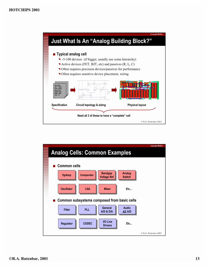
Just What Is An Analog Building Block?
Typical analog cell ~5-100 devices (if bigger, usually use some hierarchy) Active devices (FET, BJT, etc) and passives (R, L, C) Often requires precision devices/passives for performance Often requires sensitive device placement, wiring
Need all 3 of these to have a complete cell
© R.A. Rutenbar 2001
Analog Cells: Common Examples
Common cells
Common subsystems composed from basic cells
OpAmpOpAmp BandgapVoltage RefBandgap
Voltage RefComparatorComparator AnalogSwitch
AnalogSwitch
LNALNAOscillatorOscillator MixerMixer Etc...
FilterFilter GeneralA/D & D/AGeneral
A/D & D/APLLPLL Audio∆Σ∆Σ∆Σ∆Σ A/DAudio∆Σ∆Σ∆Σ∆Σ A/D
CODECCODECRegulatorRegulator I/O LineDrivers
I/O LineDrivers Etc...

HOTCHIPS 2001
©R.A. Rutenbar, 2001 14
© R.A. Rutenbar 2001
Analog Cell Design: Critical Tasks
No matter how you do it, you have to do these tasks Basic device-level circuit design
Gain 60dBUGF 111MHzPhase 60degSlew 2V/usCMRR: 60dBPSRR: 70dBTHD: 1%...
Generateproper specs
Chooseproper
circuit topology
Designproper device sizing/biasing
VinM1
Vbias2
VoutVin+
M2
M5
Gnd
Vss
MX
M8
MY
M9
Vdd
M3 M4
Rc
Vbias3
Vbias1
Cc
Cload
11/4 11/4
42/3 42/3
3/3 3/3
3/4 3/4
160/12
10pF
¿ 10pF
In- In+ 23µA54µA 3/52
Vin+ Vin-M2
Vss
Vdd
M9
M11
M7
M5
M8
M10
M4
Vout+Vout
M17 M16 M15 M14
M6
M19
M1
Vcm
Vout+
M3
Vb2
M12M13
Vb1
M18
Vb3
Vin+ Vin-M2
Vss
Vdd
M9
M11
M7
M5
M8
M10
M4
Vout+Vout
M17 M16 M15 M14
M6
M19
M1
Vcm
Vout+
M3
Vb2
M12M13
Vb1
M18
Vb3
80/4 80/4
Optimize forcentering,
yield
© R.A. Rutenbar 2001
Analog Cell Design: Critical Tasks
No matter how you do it, you have to do these tasks Basic device-level layout design
Vin+ Vin-M2
Vss
Vdd
M9
M11
M7
M5
M8
M10
M4
Vout+Vout
M17 M16 M15 M14
M6
M19
M1
Vcm
Vout+
M3
Vb2
M12M13
Vb1
M18
Vb3
From sized
schematic
Chooseproper
cell footprint
Designindividual
device geometries
Place/route devices, optimize area,coupling, etc.
vdd
vss

HOTCHIPS 2001
©R.A. Rutenbar, 2001 15
© R.A. Rutenbar 2001
Why Is This Actually Difficult?
Common misperceptions here Based mostly on familiarity with digital cells, digital libraries,
and with digital design scenarios
Myth of limited size Hey--only 50 transistors? How hard can that be to design? I dont see people obsessing over NAND gate design!
Myth of limited libraries Theres not much analog on chip, and its mostly understood
functions like A/D and D/A, so why not just design all the required cells once, put them in a library, reuse them?
© R.A. Rutenbar 2001
Reminder: Cell-Based Digital Design
Digital ASIC design Often starts from assumed library of cells (maybe some cores too) Supports changes in cell-library; assumed part of methodology Cell libraries heavily reused across different designs
DigitalHDL
LogicSynthesis
TechMapping
PhysicalDesign
Gate-Level Cell Library

HOTCHIPS 2001
©R.A. Rutenbar, 2001 16
© R.A. Rutenbar 2001
Cell-Based Design Strategies: Digital Where do digital cells come from?
Foundries:Optimized for
this fab
3rd Party IP:Emphasize
portability, quick use
Migration Tools:Old cells -> new cells
Migrate
Manual, Custom Design:Proprietary or custom library
© R.A. Rutenbar 2001
Cell-Based Design Strategies: Analog
Where do analog cells come from? Mainly manual design Often, manual redesign Almost no reuse
Why is this?
−−−−++++

HOTCHIPS 2001
©R.A. Rutenbar, 2001 17
© R.A. Rutenbar 2001
No digital abstraction to hide process No logic levels, noise margins, etc, on analog cells
Exploits physics of fab process, instead of avoiding it Individual devices designed to achieve precise behaviors Especially true with precision passive devices, which might require
separate process steps (eg, double poly for capacitors) Circuits sensitive to all aspects of device/interconnect behavior,
even modest changes due to simple dimensional shrinks
Analog Cells: Strong Fab Dependence
Cant hide behind nice 1s and 0s...
© R.A. Rutenbar 2001
Analog Cells in Digital Processes
For SoC designs, want analog in standard digital process Common problems
Low supply voltages preclude some circuit topologies
Precision structures may be hard/impossible to build if special layers are unavailable (eg, poly-poly capacitor)
Digital processes do not characterize devices for analog uses, eg, models do not capture subthreshold ops, matching, etc
Vin Vin+M2
M17
Vss
Vdd
M10
M14
M6
M4
Ibias1
M9
M13
M5
M3
M15
M11
M7 M8
M12
M16
Vout+Vout
Cc Cc
M18 M20
M25
M21 M19
M26
M31 M28 M27
M24M23
M30 M29M33
M1
Vcm
Vout+
4-high gate stack worksfine in 2µµµµm, fails indeep submicron due tolack of ∆∆∆∆VGS
Custom opamp

HOTCHIPS 2001
©R.A. Rutenbar, 2001 18
© R.A. Rutenbar 2001
Result: Analog Cells Resist Scaling/Migration
Analog cells manipulate precise electrical quantities Depend on precise physical parameters, precise device geometry Scale or migrate: process changes, so must redo circuit and layout Retarget circuit function: specs change (even a little), must redo ckt
Scale/migrate Scale/migrate/retarget
© R.A. Rutenbar 2001
Note: Feature Size Is Scaling
Min Wire Widths0.5um 0.35u 0.25u 0.18u

HOTCHIPS 2001
©R.A. Rutenbar, 2001 19
© R.A. Rutenbar 2001
Note: Electrical Interface Specs May Not
Example: currents in critical wires affects min allowed width
Min Wire Widths0.5um 0.35u 0.25u 0.18u
Min Wire Widthto Carry Current ~ 2.5mA
~1 um / mA of current,
independent offeature size
© R.A. Rutenbar 2001
Major Impact: Analog is Less Library-able
Cell design difficulty, libraries OK, so, maybe its hard to design an analog cell. So, why not just design it once, add to lib, reuse it?
Problem: leverage not same for analog libraries How big is a digital library? Big enough to get all necessary logic
functions, IO variants, timing variants, drive strengths, to first order
D Q
XFanin &fanout
variants XTiming,
latch/FF,scan
variantsX
Drivestrength(1X, 2X4X, 8X)variants
= ~1k-2kcells
Logicfunctions

HOTCHIPS 2001
©R.A. Rutenbar, 2001 20
© R.A. Rutenbar 2001
Analog Cell Libraries: Dimensionality
Problem: many continuous specs for analog cells
Cant just build a practical-size, universal analog library
−−−−++++ =
11/4 11/4
42/3 42/3
3/3 3/3
3/4 3/4
160/12
10pF
¿ 10pF
In- In+ 23µA54µA 3/52
10 independentperformancespecifications
=
Spec=LOWSpec=HIGH
variantsfor ALL
combinations
X = ~ 1000 variantsfor just this cell
© R.A. Rutenbar 2001best worst
Analog Cell Libraries: Dimensionality Dimensionality: Reality check
OK, do you really need all 1000 of those variants? Cant we make do with just a few--like we do for digital gates?
Maybe: depends on your application
Performance
Performanceworst
best
Bleeding edge...
-+
-+
At modest levels ofperformance, you may beable to survive withlimited variants, specs
-+
-+
-+
-+
-+
-+
-+
But not out here, onhigh-performance apps,where every specmatters, most areinterdependent, andthere is little slack onmeeting design goals

HOTCHIPS 2001
©R.A. Rutenbar, 2001 21
© R.A. Rutenbar 2001
Analog Cells: Design & Reuse Strategies
2 major issues How do I make it easier to design this cell in the first place? How do I avoid designing it again? Can I reuse it, wrap/buy it as IP?
Design: focuses at 3 levels Devices, cells, cores
IP/reuse: focuses on 3 strategies Hard, firm, soft IP strategies
© R.A. Rutenbar 2001
Analog Cells: Design & Reuse Strategies Simple taxonomy
Focus is onlayout reuse
Focus is onreusable circuit
& layout templates
Focus is onsynthesis, from
spec to ckt to layout
IP/REUSEhard firm soft
DESI
GN
device
cell
core
Libraries of difficult,exotic device layouts
Libs of generic celllayouts for specific fab
Libs of useful blocklayouts for specific fab
--
Parametric templatesfor schematic, layout
Parametric templatesfor useful cores
Parametric devicelayout generators
Analog ckt synthesisand layout synthesis
Mixed-signal systemassembly

HOTCHIPS 2001
©R.A. Rutenbar, 2001 22
© R.A. Rutenbar 2001
Analog Cell Design & Reuse What are people most commonly doing right now?
(Actually, theyre mostly designing by hand, one device at a time)
IP/REUSEhard firm soft
DESI
GN
device
cell
core
Libraries of difficult,exotic device layouts
Libs of generic celllayouts for specific fab
Libs of useful blocklayouts for specific fab
--
Parametric templatesfor schematic, layout
Parametric templatesfor useful cores
Parametric devicelayout generators
Analog ckt synthesisand layout synthesis
Mixed-signal systemassembly
© R.A. Rutenbar 2001
First, Look at Device-Level Issues
Question: why the emphasis on individual devices?
IP/REUSEhard firm soft
DESI
GN
device
cell
core
Libraries of difficult,exotic device layouts
Libs of generic celllayouts for specific fab
Libs of useful blocklayouts for specific fab
--
Parametric templatesfor schematic, layout
Parametric templatesfor useful cores
Parametric devicelayout generators
Analog ckt synthesisand layout synthesis
Mixed-signal systemassembly

HOTCHIPS 2001
©R.A. Rutenbar, 2001 23
© R.A. Rutenbar 2001
Analog Device IP
Basic idea Analog cells require difficult device structures May need large devices, aggressive matching, unusual precision Can save device layouts in a library, or more commonly... ... write layout generators; may be provided by your foundry Implementations vary: can use commercial frameworks (Mentor
GDT, Cadence PCELL), or write your own (C++, JAVA, etc)
DeviceIP
Gen.
Ν7
© R.A. Rutenbar 2001
Device-Level IP: What Large MeansDigital FET Analog FET

HOTCHIPS 2001
©R.A. Rutenbar, 2001 24
© R.A. Rutenbar 2001
Device-Level IP: Limited PorosityAnalog FET
Also,precision devices
almost neverallow wires
over the top,to minimize
potential coupling.
This wholeobject is
blocked forupper metals.
© R.A. Rutenbar 2001
Large Can Mean Very Large, Too
1 FET A fewcapacitors
A smallCPU core
HOTCHIPS 2001
©R.A. Rutenbar, 2001 25
© R.A. Rutenbar 2001
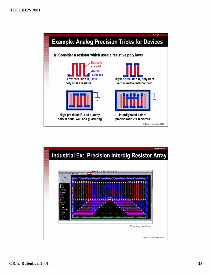
Example: Analog Precision Tricks for Devices
Consider a resistor which uses a resistive poly layer
Low-precision R,poly snake resistor
Resistive materialMetal-strappedpins Higher-precision R, poly bars
with all-metal interconnect
High-precision R, add dummybars at ends, well and guard ring
Interdigitated pair of precise-ratio 2:1 resistors
© R.A. Rutenbar 2001
Industrial Ex: Precision Interdig Resistor Array
Courtesy Neolinear

HOTCHIPS 2001
©R.A. Rutenbar, 2001 26
© R.A. Rutenbar 2001
Next, Look at Hard Analog IP
Question: how much can you reuse complete layouts?
IP/REUSEhard firm soft
DESI
GN
device
cell
core
Libraries of difficult,exotic device layouts
Libs of generic celllayouts for specific fab
Libs of useful blocklayouts for specific fab
--
Parametric templatesfor schematic, layout
Parametric templatesfor useful cores
Parametric devicelayout generators
Analog ckt synthesisand layout synthesis
Mixed-signal systemsynthesis
© R.A. Rutenbar 2001
Hard Analog Cell IP Basic idea
Hard IP (layouts) for common, generic cell functions Performance ranges estimated to target common application areas
(eg, audio, video, LAN, IO driver, etc) Available from some foundries; also some 3rd party IP shops who
design for standard digital fabs
Tend to stay away frommaximally aggressiveperformance specs;target commonmid-range performance
best worstPerformance
Performanceworst
best
Bleeding edge...
-+-
+
-+ -
+-+
-+

HOTCHIPS 2001
©R.A. Rutenbar, 2001 27
© R.A. Rutenbar 2001
Hard Analog Cell IP: Analysis Pro
Again, makes it easy to do some simple functions
Con Unlike digital libraries, unlikely that 100% of needed cells available And, cell portfolio will differ significantly from vendor to vendor
Sorry, this requirescustom analog--more design effort,impact on design risk
Your mixedsignal ASIC
Vendor 1Coverage
Vendor 2Coverage
Vendor 3Coverage
© R.A. Rutenbar 2001
Focus Now on Design & Synthesis
OK, suppose you cant just buy the analog cells you need; what can you do to help design them faster, better?
IP/REUSEhard firm soft
DESI
GN
device
cell
core
Libraries of difficult,exotic device layouts
Libs of generic celllayouts for specific fab
Libs of useful blocklayouts for specific fab
--
Parametric templatesfor schematic, layout
Parametric templatesfor useful cores
Parametric devicelayout generators
Analog ckt synthesisand layout synthesis
Mixed-signal systemsynthesis

HOTCHIPS 2001
©R.A. Rutenbar, 2001 28
© R.A. Rutenbar 2001
Cell-Level Strategies
Aside from doing everything manually, are there options?
Template-based design If you keep designing the same cells, for similar ranges of
performance, try to capture central characteristics as a template Parameters fill in the template, change resulting design
Analog synthesis For more general case, specify critical performance constraints
(electrical, geometric, etc) Synthesis tool uses numerical/geometric search to create circuit to
match your design goals
© R.A. Rutenbar 2001
Analogy from Digital World
How do people put big ASICs together today? In big pieces, compiling & synthesizing the chunks as needed
Digital ASICI need an Embedded SRAM:Use a RAM generator tool
I need a Regular Datapath:Use a Datapath compiler
I need a Register File: Use a RegFile compiler
I need 75,0000 gates of random logic:
Use logic synthesis followed by
physical synthesis

HOTCHIPS 2001
©R.A. Rutenbar, 2001 29
© R.A. Rutenbar 2001
On the Analog Side of a Mixed-Signal SoC
We want the same sort of functionality Synthesis: for the very custom cells that determine analog performance Templates: for the less custom, more regular stuff left over
Mixed-SignalASIC
I need a custom Video Amplifier
Use analog circuit & physical synthesis
I need a custom Voltage Reference
Use analog circuit & physical synthesis
I need a set of custom High-Precision PassivesUse a Device generator
I need a custom A/D Converter Use a mix of template compilers
and custom analog synthesis
© R.A. Rutenbar 2001
Template Example: CMOS Analog Cells
Manually capture regularities as procedures for high-use cells Can mix device generators, cell generators, compaction ideas, etc. Still requires significant manual setup & maintenance investment
Courtesy Koen Lampaert, Conexant

HOTCHIPS 2001
©R.A. Rutenbar, 2001 30
© R.A. Rutenbar 2001
Template Example: RF Components
Optimizes LC-oscillators fromspecs to layout [Deranter DAC00] Simulated annealing in combination
with circuit simulations and some equations FEM simulations to characterize inductor coils Auto template-based generation of VCO layout
Parameter Low resistive sub CMOS 0.35µm
High resistive sub BiCMOS 0.65µm
Ls 1.26 nH 2.3 nH Rs 6.5 Ω 5.2 Ω Rad, W, Turns 109 µm, 40 µm, 2 141 µm, 5 µm, 2 Power 32 mW 8.2 mW
Courtesy Georges Gielen, K. U. Leuven
© R.A. Rutenbar 2001
Template Example: RF Components
RF mixer, circuit & layout optimized together, [Gielen ICCAD01]
One quarter of the mixer core
Complete mixer floorplan, withquarter-piece above highlighted
An optimized layout
Courtesy Georges Gielen, K. U. Leuven

HOTCHIPS 2001
©R.A. Rutenbar, 2001 31
© R.A. Rutenbar 2001
More General Attack: Analog Synthesis
Basic idea Circuit synthesis: transform cell spec into sized/biased schematic Layout synthesis: transform device-level netlist into laid-out cell
Mimics ideas from digitallogic/layout synthesis
But, focus is transistor-level synthesis A few alternative approaches
Gain 60dBUGF 111MHzPhase 60degSlew 2V/usCMRR: 60dBPSRR: 70dBTHD: 1%............
11/4 11/4
42/3 42/3
3/3 3/3
3/4 3/4
160/12
10pF
¿ 10pF
In- In+ 23µA54µA 3/52
CircuitSynthesis
CircuitLayout
© R.A. Rutenbar 2001
Cell-Level Synthesis: Framework
Most approaches have this overall structure
Uses heuristic or numerical search Optimization engine: proposes candidate circuit solutions Evaluation engine: evaluates quality of each candidate Cost-based search: cost metric represents goodness of design
EvaluatedCircuit
Performance
Candidate CircuitDesign
OptimizationEngine
EvaluationEngine

HOTCHIPS 2001
©R.A. Rutenbar, 2001 32
© R.A. Rutenbar 2001
20 Years of Synthesis Distilled Onto 1 Slide
Optimization EngineNumericaloptimizer
(3) Symbolic analysis
Evaluation EngineAuto-derived eqns
I = K/2 W/L (Vgs-Vt)2
Optimization EngineGlobaloptimizer
(4) Simulation-Based
Evaluation EngineIndustrial simulator
Optimization Engine
You
(1) Scripting
Evaluation EngineEqns you write: I = K/2 W/L (Vgs-Vt)2
Evaluation EngineEqns you write: I = K/2 W/L (Vgs-Vt)2
Optimization Engine
(2) Equation-Based
Numericaloptimizer
© R.A. Rutenbar 2001
Eqn-Based Optimization: Example Example: posynomial-formulation [Hershenson ICCAD98]
If you can render all equations as posynomials (like polynomials, but real-valued exponents and only positive terms, eg 3x2y2.3z-2), can show resulting problem is convex, has one unique minimum
Geometric programming can solve these to optimality
Optimal trade-off curvesExample:opampcircuit
synthesized,fabbed in
TSMC0.35µµµµmCMOS
Courtesy Mar Hershenson, Stanford

HOTCHIPS 2001
©R.A. Rutenbar, 2001 33
© R.A. Rutenbar 2001
M9a
Q3a
Q1a
Q2a
M5a
Ra
CCa
M2a
M1a M1b
M2b
Rb
CCb
M3Q1b
Q3b
M5b
M4b
Q2b
CLb
Q4
Q5
GND
M6
Ibias
out+ out-
VDD
CLa
M9b
inp inn
M4a
n4
n16 n19
n1
n9
n14n17
n15
n10 n11
n12
n18
n2
n8
n0
n13
Symbolic Analysis Example Katholieke Univ. Leuven, ISAAC/SYMBA tool [Gielen JCTh95]
Courtesy Georges Gielen, KUL
+++
+
=
2
2,9,
5,5,
5,4,
4,
1,
2,0
Q
QoMoa
MmbMm
MoMo
Mm
Mm
MmV ggG
gggg
ggg
A
β
© R.A. Rutenbar 2001
95 115 13514
16
18
20
75Area (1000 sq. grids)
Folded cascode opamp, high-drive output stage 33 devs, 2 Rs, 2 Cs; 0.8um CMOS
Difficult goals High drive amplifier, 5Ωload Nominal THD, 0.1% 1kHz, 2.6V p-p input voltage
Simulation Based Example: Cells from TI Done using CMU ANACONDA tool [Phelps CICC99]
Run on CPU farm5 runs shown hereAll specs metAll specs fully simulated
Slightly overdesigned
TIs manual design
Power (mW)

HOTCHIPS 2001
©R.A. Rutenbar, 2001 34
© R.A. Rutenbar 2001
Large Sim-Based Example: TI ADSL CODEC
[R. Hester, et al.. IEEE Intl Solid-State Circuits Conf., 1999] [R. Phelps, et al., ACM/IEEE Design Automation Conf, 2000]
EQFEqualizer
1.54MHz, corner
0dB gain
AnalogLow-Pass
Filter
0-25dB/MHzgain, in
5dB/MHzsteps
ProgrammableGain
Amplifier
2.5-11.5 dBgain, in0.25dBsteps
Analog toDigital
Converter
4416KHz14bits
DigitalLow-Pass
Filter
1.1MHzcorner,
0dB gain
Decimation
Input fc 4416KHzOutput fc2208KHz
© R.A. Rutenbar 2001
EQF: What It Does
EQF = equalizer + 4th-order elliptical low-pass C-T filter Programmably amplifies signal (since attenuated by copper) Filters data from spectrum (avoiding phone voice band)
Spectral Mask
0
-20
-40
-60
-800 2 4 6 8 10 12 14 16
Freq (MHz)
Gai
n (d
B)
Gai
n (d
B)
0
-10
10
20
30
Freq (MHz)0 0.4 0.8 1.2 1.6
All 6 Eq Se ttings Flat Eq Setting
Eq0Eq1
Eq2Eq3Eq4Eq5
Eq0

HOTCHIPS 2001
©R.A. Rutenbar, 2001 35
© R.A. Rutenbar 2001
EQF Block: What It Looks Like 5 low-noise amps, ~100 passives, 36
program switches, 6 op-modes, ~400 devices, flat; ~2-3hrs to SPICE
----++++
----++++
----++++
----++++
----++++
AA
BB
Vin Vout----++++
----++++
----++++
----++++
----++++
AA
BB
Vin Vout
A B
OM
OM
OP
© R.A. Rutenbar 2001
25
50
75
100
125
1000 1100 1200 1300 1400 1500
TI Hand CMU2CMU3 CMU1
CMU Synthesis Results: Noise vs Area
Max Noise 25-1104KHz @25oC (nV/Hz1/2)
Smaller &less noise
Biggest &least noise
Area (1000 square grids)
Full sizing/biasing ~10hours on 20 CPUs; all TI specs met

HOTCHIPS 2001
©R.A. Rutenbar, 2001 36
© R.A. Rutenbar 2001
Synthesis Results: Spectral Mask
~ 2 months designed manually Synthesized automatically overnight 0 2 4 6 8 10 12 14 16
Freq (MHz)
Eq0 Spectral Mask
0
-20
-40
-60
-80G
ain
(dB
)
Eq0 Passband
Freq (MHz)0 0.4 0.8 1.2 1.6
0-2
Gai
n (d
B)
-4-6
-8
CMU1
CMU2
CMU3
TI Hand
© R.A. Rutenbar 2001
One More Messy Issue: Design Centering
Cannot ignore this entirely in any analog design flow Optimization-based attacks can find bad corners of design space
2 broad, overall strategies Use first-order heuristics in numerical synthesis, then run centering Combine full statistical optimization in with numerical synthesis Examples: [Mukherjee TCAD00], [Debyser, ICCAD98]
6065707580859095
4 .5 4 .7 4 .9 5 .1 5 .3 5 .5
Manual designPhase Margin
Input spec:Phase margin > 77°at Vdd = 5.0V
5.0V dd (V)
Synthesis
If ignore range / mfg variations,you only get what you ask for: Phase OK at 5V, but not elsewhere

HOTCHIPS 2001
©R.A. Rutenbar, 2001 37
© R.A. Rutenbar 2001
Example: Centering Heuristics in Synthesis
Simple designer-derived constraints in ANACONDA synthesis Require matched devices to be big; sensitive devices to be far
enough into desired region of operation (eg, 250mV above VT)
2500
02500 3000 (V/V)
(V/V)
2000
2000 3000
60
120
0
60
120
Hand design
Synthesizeddesign
ExampleMonte Carlo
spread for a smallTI opamp
3σσσσ process, +/-10% supply
& temp. variation
Plots showlow-frequency
gain formanual, auto
designs
© R.A. Rutenbar 2001
Cell-Level Analog Layout Synthesis
Basic task
Major strategies Enhanced polygon-editing Analog compaction & templates Physical synthesis: full device-level custom place/route
11/4 11/4
42/3 42/3
3/3 3/3
3/4 3/4
160/12
10pF
¿ 10pF
In- In+ 23µA54µA 3/52 Layout
Synthesis
From schematic +geometric constraintsto physical layout

HOTCHIPS 2001
©R.A. Rutenbar, 2001 38
© R.A. Rutenbar 2001
Analog-Specific Optimizations: Place/Route Placement symmetric and diffusion merging
Routing: differential symmetric and coupling avoidanceWiring task
withObstacle
No symmetryNo crosstalk
SymmetryNo crosstalk
SymmetryCrosstalk
No symmetryNo merging
SymmetryNo Merging
SymmetryMerging
[Cohn, JSSC91]
© R.A. Rutenbar 2001
Small Physical Synthesis Example: Close-up
Commercial tools emerging Neolinears
NeoCell
This example CMOS ~50 devices Layout < 1 hr
Courtesy Neolinear

HOTCHIPS 2001
©R.A. Rutenbar, 2001 39
© R.A. Rutenbar 2001
Large Physical Synthesis Example
Proprietary CMOS comparator auto-layout from NeoCell
Courtesy Neolinear
© R.A. Rutenbar 2001
Subsystem Example: Cells + Glue Circuits
CELL1 CELL1
CELL2 CELL2
GLUE
MORE GLUE
Courtesy RocketChips and Neolinear
HOTCHIPS 2001
©R.A. Rutenbar, 2001 40
© R.A. Rutenbar 2001
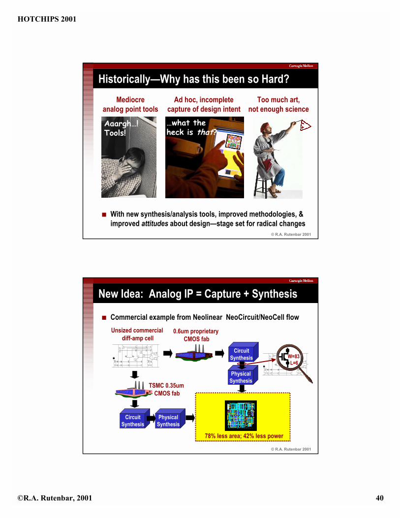
HistoricallyWhy has this been so Hard?
With new synthesis/analysis tools, improved methodologies, & improved attitudes about designstage set for radical changes
Too much art,not enough science
Mediocreanalog point tools
Aaargh!Tools!
Ad hoc, incompletecapture of design intentwhat theheck is that?
© R.A. Rutenbar 2001
New Idea: Analog IP = Capture + Synthesis
Commercial example from Neolinear NeoCircuit/NeoCell flowUnsized commercial
diff-amp cell
PhysicalSynthesis
CircuitSynthesis
PhysicalSynthesis
0.6um proprietary CMOS fab
TSMC 0.35um CMOS fab
78% less area; 42% less power
CircuitSynthesis W=83
L=6

HOTCHIPS 2001
©R.A. Rutenbar, 2001 41
© R.A. Rutenbar 2001
Outline
Quick tour of mixed-signal System-on-Chip (SoC) design
Design problems & strategies for analog building blocks
Design problems & strategies for mixed-signal chips
Talk emphasis We do all this analog design by hand, as painful full custom, today That has got to changetoo many opportunities, too few designers What are the prospects for buy itor reuse it for analog? This is the hot topic in analog today: analog intellectual property
© R.A. Rutenbar 2001
Whats Left to Do: Chip-Level Design
OK, you design/buy/synthesize all your cellsthen what?Chip-level design. (and, problems dont get easier)
IP/REUSEhard firm soft
DESI
GN
device
cell
core
Libraries of difficult,exotic device layouts
Libs of generic celllayouts for specific fab
Libs of useful blocklayouts for specific fab
--
Parametric templatesfor schematic, layout
Parametric templatesfor useful cores
Parametric devicelayout generators
Analog ckt synthesisand layout synthesis
Mixed-signal systemassembly

HOTCHIPS 2001
©R.A. Rutenbar, 2001 42
© R.A. Rutenbar 2001
Hard Analog Core IP (= Mixed-Signal IP) Recent commercial idea
Dont focus on basic cells, focus on bigger mixed-signal cores Industry standards fix many specs; target big ASIC foundries Interesting technical (& business) issues here
MixSigCore
PLLA/D, D/AFilterCodecEthernet IOFirewire IO, .
Hide low-level analog;basic cells hand-crafted to exploit foundry process
cell cell cell
cell cell cell
Digital blocks
IP/REUSEhard firm soft
DESI
GN
device
cell
core
Libraries of difficult,exotic device layouts
Libs of generic celllayouts for specific fab
Libs of useful blocklayouts for specific fab
--
Parametric templatesfor schematic, layout
Parametric templatesfor useful cores
Parametric devicelayout generators
Analog ckt synthesisand layout synthesis
Mixed-signal systemassembly
© R.A. Rutenbar 2001
Template-Based System Layout Example
Analogy: just like digital datapath generators Can exploit analog regularities you know; procedurally generate
[ISSCC99]J. Vandenbussche, G. Van
der Plas, A. Van den Bosch, W. Daems, G. Gielen,
M. Steyaert, W. Sansen
CURRENT SOURCE ARRAY
SWATCH ARRAY
FULL DECODER
DIGITALCLOCKDRIVER
ANALOGCLOCKDRIVER
14-bit 150-Ms/s 0.5um CMOS DAC
Courtesy Georges Gielen, K.U. Leuven

HOTCHIPS 2001
©R.A. Rutenbar, 2001 43
© R.A. Rutenbar 2001
Mixed-Signal SoC Revisited
We want block-level IP & assembly for both digital and analog Synthesis: for the very custom, performance-sensitive circuits Templates: for the less custom, more regular stuff left over
Mixed-SignalASIC
I need a custom Video Amplifier
Use analog circuit & physical synthesis
I need a set of custom High-Precision PassivesUse a Device generator
I need a custom A/D Converter Mix of templates and
custom analog synthesis
I need an Embedded SRAM:Use a RAM generator tool
I need 75,0000 gates of random logic:
Use logic synthesis followed by
physical synthesis
© R.A. Rutenbar 2001
Authored with Cadence
DSP Core
PLL Clock
Authored with Neolinear and Cadence
Results Converter ( FFT )
Authored with Cadence
RAM ( 128 x 16 ) Glue Logic
RAM ( 256 x 16 )
I/O pads
ROM ( 512 x 16A )
Authored with Artisan ROM CompilerAuthored with
Artisan RAM Compiler
Courtesy Artisan, Cadence and Neolinear
Example: Dual-Tone Multi-Frequency DecoderAnalog

HOTCHIPS 2001
©R.A. Rutenbar, 2001 44
© R.A. Rutenbar 2001
Top block & support logicassembled using Cadence
Authored with Cadence
Authored with NeoCell
Authored with NeoCell
Authored with CadenceAuthored with Cadence
Counter (3-bit)
Voltage-ControlledOscillator
Charge Pump
Divider ( 2-bit )
Phase Detector
Buffers
Bias Xtors
Cadence ® Generic PDK.18 6LM Generic Process
Decoder PLLPushing Inside the PLL All analog done via custom synthesis on this design
Courtesy Cadence and Neolinear
© R.A. Rutenbar 2001
Next Problem: Mixed-Signal Chip Assembly
or, When Bad Things Happen to Good Cells Noise upsets on delicate/precise analog
From noisy digital wires nearby From noisy shared substrate and from noisy power grid
Thermal issues Large digital blocks switching, or large analog devices: heat Temperature changes can affect precision analog
Solutions Segregate (away from digital) Isolate, shield (from noise)
Analog

HOTCHIPS 2001
©R.A. Rutenbar, 2001 45
© R.A. Rutenbar 2001
Substrate
Noise At Mixed-Signal Chip Level
L wirebondsChip/package interconnect
pad
pad
Power businterconnect
Power businterconnect
pad
Analog(Sensitive)
Coupled through supply rails and common substrate Precise analog biasing easily vulnerable to voltage upset
Digital(Noisy)
© R.A. Rutenbar 2001
One Assembly Example: IBM Data Channel Digital switching is the source of (almost) all evil for analog
Substrate
Ground
Power
Switc
hing
curre
nt
Power
Courtesy Bob Stanisic/Tim Schmerbeck, IBM
5mV
Measurements from IBM disk data channel; Substrate noise spec 4mV -- exceeded
Substrate Gnd
VDD

HOTCHIPS 2001
©R.A. Rutenbar, 2001 46
© R.A. Rutenbar 2001
Another Example: TI High-Speed Video DAC
Texas InstrumentsHigh-speed video DAC, ~1994
30 90 150 210
0
1.4
4.2
2.8
-1.4
Substrate800mV p-p
DAC
Time (ns)
Volts
ADC codes
Samples
Measured chipperformance at 14.4MHz
Sparklecodes,errors
Courtesy Texas Instruments
© R.A. Rutenbar 2001
CAD Solution: Power Grid Synthesis Auto power grid synthesis
Re-synthesized IBM grid Power grid routed, sized Power IOs assigned Substrate contacts configured Decoupling caps added
Vnoise [mV]
0102030405060
Bus only
+I/O cells
+Subcons
+Caps
Vdrop [mV]
0
20
40
60
80
100
Bus only
+I/O cells
+Subcons
+Caps
Dynamic Noise (mV) Static IR Drop (mV)[Stanisic JSSC 94]
AnalogAnalog

HOTCHIPS 2001
©R.A. Rutenbar, 2001 47
© R.A. Rutenbar 2001
Mixed-Signal Chip-Level Assembly Today
Embarrassingly ad hoc Lots of guessing (and lots of praying) about floorplan, global signal
routing, block-level isolation structures, etc Often vastly over-conservative; sometimes just plain wrong Often takes a few silicon spins to iron out ( few may mean 5-10 at
RF and higher frequencies)
Where the action is Full-chip and package extraction and simulation for noise coupling Smarter circuit design methodologies for noise immunity (think
echo cancelation, but replace echo with substrate noise)
© R.A. Rutenbar 2001
Conclusions
Analog circuits: here to stay In an SoC world, big systems need to talk to the external world The world is analog (get used to it); analog does this communication
Mixed-signal design realities Analog cells != digital cells Not as easily library-able; dont scale; dont migrate Tightly bound to fab process, difficult precision requirements Chip level assembly is nasty
Design strategies Less art, more science: better methodologies, real synthesis tools Analog IP: design for migrating, retargeting is the next big thing

HOTCHIPS 2001
©R.A. Rutenbar, 2001 48
© R.A. Rutenbar 2001
Where all this Analog IP Stuff is Heading
Analog folks want IP / reuse, too
Analog SynthesisMicrosoftMicrosoftMicrosoftMicrosoft
NewLow
Price!
NewNewLowLow
Price!Price!
Analog IP
© R.A. Rutenbar 2001
Select References
General Analog CAD Survey R. A. Rutenbar, "Analog Design Automation: Where are We? Where are we Going?", Proc.
IEEE CICC, May 1993. L. R. Carley, G. Gielen, R. A. Rutenbar, W. Sansen, "Synthesis Tools for Mixed-Signal ICs:
Progress on Frontend and Backend Strategies, Proc. ACM/IEEE DAC, June 1996. G. G. E. Gielen, R. A. Rutenbar, Computer Aided Design of Analog and Mixed-Signal
Integrated Circuits, Proceedings of the IEEE, December 2000. Computer Aided Design of Analog and Mixed-Signal ICs, B. Antao, G. Gielen, R. Rutenbar,
editors, IEEE Press, to appear 2001.
IP Issues Steve Ohr, Analog IP Slow to Start Trading, EETimes, Issue 1053, March 22 1999.
http://www.eet.com (Steve Ohr covers analog design/EDA for EETimes) K.C. Murphy, A Time for Analog Design, Electronic News Online, August 2 1999.
http://www.electronicnews.com/enews/BackIssues/BackIssues.asp http://www.vsia.com -- Virtual Socket Interface Alliance working on specs for interchange of
analog IP

HOTCHIPS 2001
©R.A. Rutenbar, 2001 49
© R.A. Rutenbar 2001
Select References Analog Synthesis
M.G.R. DeGrauwe et. al, IDAC: An Interactive Design Tool for Analog CMOS Circuits, IEEE Journal of Solid-State Circuits, December 1987.
H.Y. Koh, C.H. Sequin, P.R. Gray, OPASYN: A Compiler for CMOS Operational Amplifiers, IEEE Transactions on CAD, Feb. 1990.
R. Harjani, R.A. Rutenbar and L. Richard Carley, OASYS: A Framework for Analog Circuit Synthesis, IEEE Transactions on CAD, Dec. 1989.
G. Gielen, Walscharts, W. Sansen, Analog circuit design optimization based on symbolic analysis and simulated annealing, IEEE Journal of Solid-State Circuits, June 1990.
J. P. Harvey, M.I. Elmasry and B. Leung, STAIC: An Interactive Framework for SynthesizingCMOS and BiCMOS Analog Circuits, IEEE Transactions on CAD, Nov. 1992.
P.C. Maulik, L.R. Carley and R.A. Rutenbar, Integer Programming Based Topology Selection of Cell-Level Analog Circuits, IEEE Transactions on CAD, April 1995.
B. Antao and A. Brodersen, ARCHGEN: Automated Synthesis of Analog Systems, IEEE Transactions on VLSI Systems, June 1995.
W. Kruiskamp and D. Leenaerts, DARWIN: CMOS Opamp Synthesis by Means of a Genetic Algorithm, Proc. 32nd ACM/IEEE DAC, pp. 433-438, 1995.
G. Gielen, et al., An analog module generator for mixed analog/digital ASIC design, John WileyInternational Journal of Circuit Theory and Applications, Vol. 23, pp. 269-283, July-August 1995.
J. Crols, S. Donnay, M. Steyaert and G. Gielen, A high-level design and optimization tool for analog RF receiver front-ends, Proc. IEEE/ACM ICCAD, pp. 550-553, November 1995.
© R.A. Rutenbar 2001
Select References Analog Synthesis, cont.
F. Medeiro, F. Fernandez, R. Dominguez-Castro, A. Rodriguez-Vazquez, A Statistical Optimization Based Approach for Automated Sizing of Analog Cells, Proc. ACM/IEEE ICCAD, 1994.
E.S. Ochotta, R. A.Rutenbar and L.R. Carley, Synthesis of High-Performance Analog Circuits in ASTRX/OBLX, IEEE Transactions on CAD, March 1996.
M. Hershenson, S. Boyd, T. Lee, GPCAD: a Tool for CMOS Op-Amp Synthesis, Proc. ACM/IEEE ICCAD, pp. 296-303, 1998
M. Krasnicki, R. Phelps, R. Rutenbar, L. R. Carley, MAELSTROM: Efficient Simulation-Based Synthesis for Custom Analog Cells, Proc ACM/IEEE DAC, June 1999.
R. Phelps, M. Krasnicki, R. Rutenbar, L. R. Carley, J. Hellums, ANACONDA: Robust Synthesis of Analog Circuits Via Stochastic Pattern Search, Proc. IEEE CICC., May 1999.
R. Phelps, M. Krasnicki, R. Rutenbar, L. R. Carley, J. Hellums, A Case Study of Synthesis for Industrial-Scale Analog IP: Redesign of the Equalizer/Filter Frontend for an ADSL CODEC, Proc. ACM/IEEE DAC, June 2000.
R. Phelps, M. Krasnicki, R. Rutenbar, L. R. Carley, J. Hellums, ANACONDA: Simulation-Based Synthesis of Analog Circuits Via Stochastic Pattern Search, IEEE Transactions on CAD, June 2000.
T. Mukherjee, L.R. Carley and R.A. Rutenbar, Efficient Handling of Operating RangeandManufacturing Line Variations in Analog Cell Synthesis," IEEE Transactions on CAD, Aug 2000.
G. Debyser, G. Gielen, Efficient analog circuit synthesis with simultaneous yield and robustness optimization, Proc. IEEE/ACM ICCAD, pp. 308-311, November 1998.
C. De Ranter, et al., CYCLONE: automated design and layout of RF LC-oscillators, Proc. ACM/IEEE DAC, June 2000.

HOTCHIPS 2001
©R.A. Rutenbar, 2001 50
© R.A. Rutenbar 2001
Select References Symbolic Analysis
G. Gielen, H. Walscharts, W. Sansen, "ISAAC: A Symbolic Simulator for Analog Integrated Circuits, " IEEE Journal of Solid-State Circuits, Vol 24, No. 6, pp. 1587-1597, Dec 1989
F. Fernandez, A Rodriguez-Vazquez, J. Huertas, "Interactive AC Modeling and Characterization of Analog Circuits Via Symbolic Analysis," Kluwer Journal on Analog Integrated Circuits and Signal Processing, Vol. 1, pp. 183-208, November 1991.
J. Starzyk,, A. Konczykowska, "Flowgraph Analysis of Large Electronic Networks, IEEE Transactions on Circuits and Systems, Vol. 33, No. 3, pp 302-315, March 1986.
B. Li, D. Gu, "SSCNAP: A Program for Symbolic Analysis of Switched Capacitor Circuits, " IEEE Transactions on CAD, Vol. 11, No. 3, pp. 334-340, March 1992.
P. Wambacq, F. Fernandez, G. Gielen, W. Sansen, A. Rodriguez-Vazquez, "Efficient symbolic generation of approximated small-signal characteristics of analog integrated circuits," IEEE Journal of Solid-State Circuits, pp. 327-330, March 1995.
Q. Yu and C. Sechen, "A Unified Approach to the Approximate Symbolic Analysis of Large Analog Integrated Circuits, IEEE Trans. Circuits and Sys-I, vol.43, pp 656-669, August 1996
Q. Yu and C. Sechen, "Efficient Approximation of Symbolic Network Functions Using MatroidIntersection Algorithms," IEEE Transactions on CAD, vol. 16, no. 10. pp. 1073-1081, Oct. 1997.
C. Shi, X. Tan, "Symbolic Analysis of Large Analog Circuits with Determinant Decision Diagrams," Proc. ACM/IEEE ICCAD, pp. 366-373, 1997.
P. Wambacq, G. Gielen, P. Kinget, W. Sansen, High-frequency distortion analysis of analog integrated circuits, IEEE Trans. Circuits and Sys-I, Vol. 46, No. 3, pp. 335-345, March 1999
© R.A. Rutenbar 2001
Select References Analog Layout
J. Rijmenants, J.B. Litsios, T.R. Schwarz, M.G.R. Degrauwe, "ILAC: An Automated Layout Tools for Analog CMOS Circuits," IEEE Journal of Solid-State Circuits, Vol. 24, No. 4, pp. 417-425, April 1989.
J.M. Cohn, D.J. Garrod, R.A. Rutenbar, L.R. Carley, "KOAN/ANAGRAM II: New Tools for Device-Level Analog Placement and Routing," IEEE Journal of Solid-State Circuits, Vol. 26, No. 3, March 1991.
U. Choudhury, A Sangiovanni-Vincentelli, "Automatic Generation of Parasitic Constraints for Performance-Constrained Physical Design of Analog Circuits," IEEE Transactions on CAD, Vol. 12, No. 2, pp. 208-224, February 1993.
E. Malavasi, E. Felt, E. Charbon and A. Sangiovanni-Vincentelli, "Automation of IC Layout with Analog Constraints, " IEEE Transactions on CAD, vol. 15, no. 8, August 1996.
K. Lampaert, G. Gielen, W. Sansen, "A Performance-Driven Placement Tool for Analog Integrated Circuits," IEEE Journal of Solid-State Circuits, Vol. 30, No. 7, pp. 773-780, July 1995.
E. Malavasi, E. Felt, E. Charbon, A. Sangiovanni-Vincentelli, "Symbolic Compaction with Analog Constraints, " John Wiley International Journal on Circuit Theory and Applications, Vol.23, No.4, pp. 433-452, July/Aug. 1995
E. Malavasi, D. Pandini, "Optimum CMOS Stack Generation with Analog Constraints," IEEE Transactions on CAD, Vol. 14, No. 1, pp. 107-12, Jan. 1995.
B. Basaran, R.A. Rutenbar, An O(n) Algorithm for Optimum CMOS Device Stacking with Analog Constraints, Proc. ACM/IEEE DAC, June 1996.
G. Van der Plas, J. Vandenbussche, G. Gielen, W. Sansen, Mondriaan: a tool for automated layout synthesis of array-type analog blocks, proceedings IEEE CICC, pp. 485-488, May 1998.

HOTCHIPS 2001
©R.A. Rutenbar, 2001 51
© R.A. Rutenbar 2001
Select References
Analog Layout Mitra, R.A. Rutenbar, L.R. Carley, D.J. Allstot, "Substrate-Aware Mixed-Signal Macrocell
Placement in WRIGHT," IEEE Journal of Solid-State Circuits, Vol. 30, No. 3, pp. 269-278, March 1995.
S. Mitra, S. Nag, R.A. Rutenbar, and L.R. Carley, "System-Level Routing of Mixed-Signal ASICs in WREN," Proc. ACM/IEEE ICCAD, November 1992.
B.R. Stanisic, N.K. Verghese, R.A. Rutenbar, L.R. Carley, D. J. Allstot, "AddressingSubstrateCoupling in Mixed-Mode ICUs: Simulation and Power Distribution Synthesis," IEEE Journal of Solid-State Circuits, Vol. 29, No. 3, March 1994.
G. Gielen et al, A Layout Aware Synthesis Methodology for RF Circuits, to appear ACM/IEEE ICCAD, Nov 2001.