Embed Size (px)
Citation preview
GaN Systems 1
Design considerations of Paralleled GaN HEMT-based Half Bridge Power Stage
Last update: May 18, 2018
GaN Systems 2
Contents
Paralleling design considerations
Layout considerations for paralleling GaN
Design example of 4x paralleled GaN power stage
Experimental results

GaN Systems 3
Paralleling design considerations
Design parameters Effect on paralleling Desired RDS(on) Affect static current sharing. Positive temperature co-efficient for self-balancing
Gate threshold, VGS(th) Impact dynamic current sharing during turn-on and off. Lower Vth results in earlier turn-on and higher switching current/loss which creates positive feedback
Tight distribution, temperature independent or positive temperature co-efficient
Trans-conductance, gm Impact dynamic current sharing during turn-on and off.
Tight distribution, temperature independent or negative temperature co-efficient
Circuit design and layout
Balanced circuit layout are important for dynamic current sharing and stability of the paralleling operation. This is particularly critical for high speed power switches such as GaN/SiC
Minimize and equalize all layout parasitics to reduce circuit mismatch
Thermal Affect the device temperature difference. Tjvariation may cause dynamic or static current sharing issues depending on device characteristics.
All paralleled devices should have similar thermal resistance and installed on same heatsink for good thermal balance.
What are key considerations when paralleling power switches:

GaN Systems 4
RDS(on) vs TJ
GaN E-HEMT has positive temperature co-efficient RDS(on) Compared to SiC, strong temperature dependency of RDS(on) of GaN helps the current
sharing in parallel operationSiC RDS(on) vs TJ
NTC Region
GaN E-HEMT RDS(on) vs TJ
PTC Region
GaN Systems 5
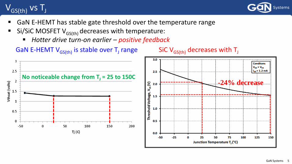
VGS(th) vs TJ
GaN E-HEMT has stable gate threshold over the temperature range Si/SiC MOSFET VGS(th) decreases with temperature:
Hotter drive turn-on earlier – positive feedbackSiC VGS(th) decreases with TJGaN E-HEMT VGS(th) is stable over TJ range
No noticeable change from TJ = 25 to 150C-24% decrease
GaN Systems 6
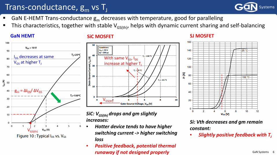
Trans-conductance, gm vs TJ GaN E-HEMT Trans-conductance gm decreases with temperature, good for paralleling This characteristics, together with stable VGS(th), helps with dynamic current sharing and self-balancing
VGS(th)
gm = ΔIDS/ ΔVGS
GaN HEMT
SiC: VGS(th) drops and gm slightly increases:• Hotter device tends to have higher
switching current -> higher switching loss
• Positive feedback, potential thermal runaway if not designed properly
VGS(th)
SiC MOSFET
IDS decreases at same VGS at higher TJ
With same VGS, IDSincrease at higher TJ
SJ MOSFET
Si: Vth decreases and gm remain constant:• Slightly positive feedback with TJ

GaN Systems 7
VGSIQ1 @ TJ = 25C
IQ2 @ TJ = 125C
2x GS66508T paralleled 400V/30A turn-on waveforms with different TJ
Eon=92uJ
Eon=58uJ
Effect of gm on switching transient Negative feedback for self balancing in parallel: TJ ↗ - gm ↘ - ID@switching↘ - Eon ↘ - TJ ↘

GaN Systems 8
Circuit layout - Low inductance of GaNPX® packageGaNPX® package improves the paralleling performance and stability
Traditional package has high source inductance that impacts paralleling performance GaNPX® package has ultra low Ls compared to traditional package Top-cooled T package features symmetric dual gate pads for easier layout
GaNPX® T PackageGS66516T (650V/25mΩ)
Top side Bottom side
Package Source inductance Ls=0.05nH
Ansys Q3D 3D modeling of GS66516T
GD
S
Ls = ~10-15nH
TO-247 Package inductance
GaN Systems 9
G
G
S
S
D
D
Q1
Q2
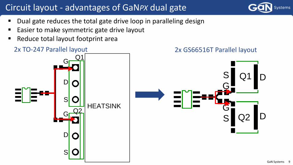
Circuit layout - advantages of GaNPX dual gate Dual gate reduces the total gate drive loop in paralleling design Easier to make symmetric gate drive layout Reduce total layout footprint area
2x TO-247 Parallel layout 2x GS66516T Parallel layout
HEATSINK
G
D
S
G
D
S
Q1
Q2
GaN Systems 10
Key design considerations for paralleling GaN
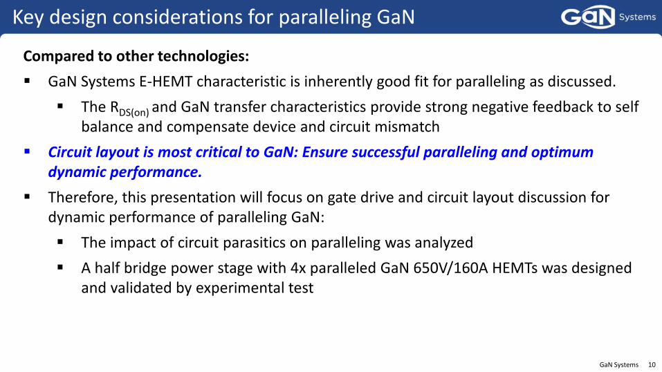
Compared to other technologies: GaN Systems E-HEMT characteristic is inherently good fit for paralleling as discussed.
The RDS(on) and GaN transfer characteristics provide strong negative feedback to self balance and compensate device and circuit mismatch
Circuit layout is most critical to GaN: Ensure successful paralleling and optimum dynamic performance.
Therefore, this presentation will focus on gate drive and circuit layout discussion for dynamic performance of paralleling GaN: The impact of circuit parasitics on paralleling was analyzed A half bridge power stage with 4x paralleled GaN 650V/160A HEMTs was designed
and validated by experimental test
GaN Systems 11
Contents
Paralleling design considerations
Layout considerations for paralleling GaN
Design example of 4x paralleled GaN power stage
Experimental results
GaN Systems 12
CDC
LD3
LCS3
LD4
LCS4
Q3 Q4
LP1
...
LG3 RG3 LG4 RG4
LDR8
LDR6
LD1
LCS1
LD2
LCS2
Q1 Q2LG1 RG1 LG2 RG2
LDR4
LDR2
...
Gate DriversGaN Enhancement-mode HEMT Half Bridge
LP2
C4
C5
LDR5
LDR7
C2
C3
LDR1
LDR3
RS3 RS4
RS1 RS2
LS3 LS4
LS1 LS2
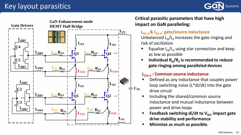
Key layout parasiticsCritical parasitic parameters that have high impact on GaN paralleling:
LG1-4 & LS1-4: gate/source inductanceUnbalanced LG/LS increases the gate ringing and risk of oscillation Equalize LG/LS using star connection and keep
as low as possible Individual RG/RS is recommended to reduce
gate ringing among paralleled devices
LCS1-4 : Common source inductance Defined as any inductance that couples power
loop switching noise (L*di/dt) into the gate drive circuit
Including the shared/common source inductance and mutual inductance between power and drive loops
Feedback switching di/dt to VGS, impact gate drive stability and performance
Minimize as much as possible.

GaN Systems 13
Gate drive design for paralleled GaN For high current paralleling design, a small negative gate drive turn-off bias is recommended
for lower turn-off loss and more robust gate drive. Recommend to use -3V to -5V with synchronous driving for optimum efficiency.
Create bipolar gate drive from single power supply using a 6.2V Zener. Negative gate drive bias (VEE) is defined by PS1 output – Vzener(6V)
Use small values (1-2Ω) for distributed gate and source resistance: R3/R5 and R6/R7 Total turn-on RG_ON = R4 + R3(R5) +R6(R7). Turn off RG_OFF = R3(R5) + R6 (R7)
U1
SI8271GB-IS
VI1
VDDI2
GNDI3
EN4
GNDA5
VO-6
VO+7
VDD8
VCCR3
1R
Q2
GS66516T
1
2
43
R5
1R
R4
4.7
R84.7K
C7
1uFGND_GD
C5
1uFGND_GD
R6
1R
R7
1R
PS1
ISO DC/DC
GND1
VIN2
+VO5
0V4
NC
8
C34.7uFC0805
0V
VCC
C14.7uFC0805 R1
2.2KR0805
VDD
Q1
GS66516T
1
2
43
0V
C60.1uF
PWM_IN
EN
ISOLATION
DRAIN
SOURCE
D1ZENER 6.2V
R21K
GD_GND
C24.7u
VDD
C44.7u
VEE
VEE
GD_GND
GaN Systems 14
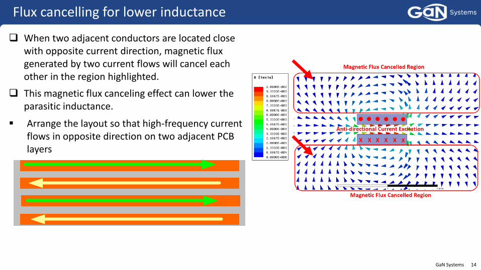
Flux cancelling for lower inductance
When two adjacent conductors are located close with opposite current direction, magnetic flux generated by two current flows will cancel each other in the region highlighted.
This magnetic flux canceling effect can lower the parasitic inductance.
Arrange the layout so that high-frequency current flows in opposite direction on two adjacent PCB layers
GaN Systems 15
Side
Vie
wTop Layer
Bottom Layer
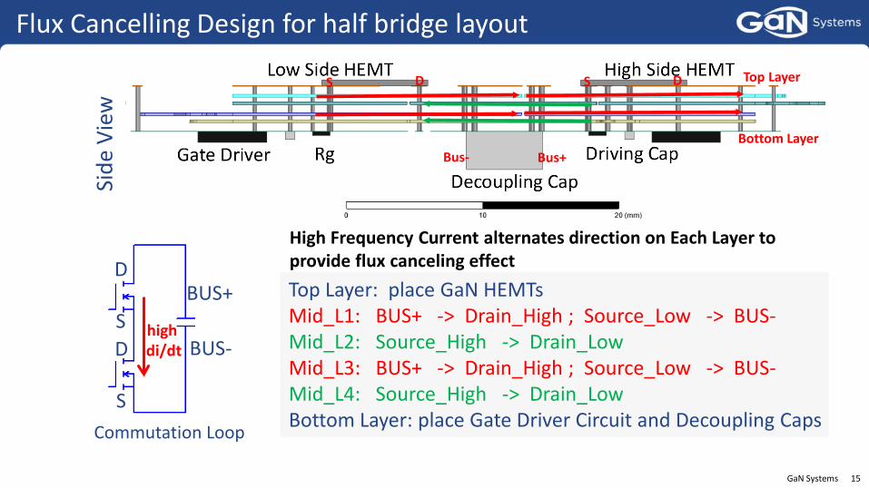
Flux Cancelling Design for half bridge layout
Top Layer: place GaN HEMTsMid_L1: BUS+ -> Drain_High ; Source_Low -> BUS-Mid_L2: Source_High -> Drain_LowMid_L3: BUS+ -> Drain_High ; Source_Low -> BUS-Mid_L4: Source_High -> Drain_LowBottom Layer: place Gate Driver Circuit and Decoupling Caps
BUS+
BUS-
S
D
High Frequency Current alternates direction on Each Layer to provide flux canceling effect
DS DS
Bus+Bus-
S
D
Commutation Loop
high di/dt

GaN Systems 16
CDC
LD3
LCS3
LD4
LCS4
Q3 Q4
LP1
...
LG3 RG3 LG4 RG4
LDR8
LDR6
LD1
LCS1
LD2
LCS2
Q1 Q2LG1 RG1 LG2 RG2
LDR4
LDR2
...
Gate DriversGaN Enhancement-mode HEMT Half Bridge
LP2
C4
C5
LDR5
LDR7
C2
C3
LDR1
LDR3
RS3 RS4
RS1 RS2
LS3 LS4
LS1 LS2
Comparison with Benchmark
State-of-Arts EmodeGaN HEMTs
Power Module [1]
GaN Systems Solution: only 25% LLoop of the Best Counterparts: Low inductance GaNPX® package Flux cancelling PCB design
[1] F.Luo, Z.Chen, L.Xue, P.Mattavelli, D.Boroyevich, B.Hughes, “Design Considerations for GaN HEMT Multichip Half- bridge Module for High-Frequency Power Converters”
0.7nH
Commutation Loop
GaN Systems 17
Contents
Paralleling design considerations
Layout considerations for paralleling GaN
Design example of 4x paralleled GaN power stage
Experimental results
GaN Systems 18
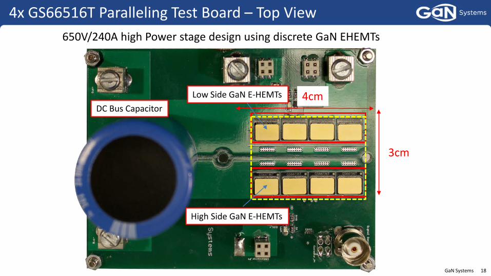
4x GS66516T Paralleling Test Board – Top View
Low Side GaN E-HEMTs
High Side GaN E-HEMTs
DC Bus Capacitor
650V/240A high Power stage design using discrete GaN EHEMTs
4cm
3cm
GaN Systems 19
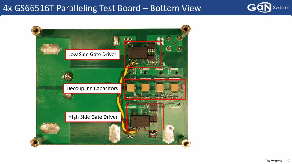
4x GS66516T Paralleling Test Board – Bottom View
Decoupling Capacitors
Low Side Gate Driver
High Side Gate Driver
GaN Systems 20
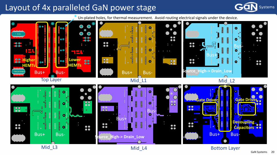
Mid_L1 Mid_L2
Mid_L3 Mid_L4 Bottom Layer
Bus+ Bus-
Bus+
Bus-
Source_High-> Drain_Low
Bus+ Bus-
Bus+Bus-
Source_High-> Drain_Low Bus+ Bus-
Decoupling Capacitors
Layout of 4x paralleled GaN power stage
Gate DriverGate Driver
Top LayerBus+ Bus-
Higher HEMTs
LowerHEMTs
* Un-plated holes, for thermal measurement. Avoid routing electrical signals under the device.
*
*
*
**
*

GaN Systems 21
Optimum Paralleling Layout for GaN HEMT (4x GS66516T)Top side with 4x GS66516T in half bridge Bot side with gate driver
Note symmetric gate drive layout:- Utilize the dual gate on
GS66516T GaNPx- Gate resistor on each gate
Gate driverGate driverGate driver
BUS+
BUS-
DC Link Cap
HV decoupling Cap
* Un-plated holes, for thermal measurement. Avoid routing electrical signals under the device.
* *
*
*
**
*
*
*
*

GaN Systems 22
Contents
Paralleling design considerations
Layout considerations for paralleling GaN
Design example of 4x paralleled GaN power stage
Experimental results

GaN Systems 23
400V/240A double pulse hard Switching test waveformsDUT: 4x GS66516T in parallel; Freewheeling: 4x GS66516T in parallelCondition: VBUS=400V, IDS_ON=231A, IDS_OFF=240A, VGS=+6.8V/-5V, RG_ON=4.55ohm, RG_OFF=1.25 ohm.
Vds_DUT(C1)
Freewheeling
DUT
iL(C2)
VGS=-5V
Double Pulse
Vds_DUT(C1:100V/div)
iL(C2:100A/div)
No-Derating Paralleling of GaN HEMTs. Hard switched up to full rated current with clean waveform. 400V/240A Hard Switching Capability with ~200V VDS Margin
Experimental Waveform
L=50uH Hard switching on/off
Vspike=52V
iOFF =240A
Measurement Setup: Lecroy WaveSurfer 10M Oscilloscope, HVD3106 Differential Probe(C1), CWT-3LFB mini Rogowski Coil(C2)
On: dv/dt=19.5V/nS Off: dv/dt=59.6V/nS
GaN Systems 24
Summary Paralleling discrete GaN is desired to achieve higher power output GaN Systems E-HEMT device characteristics are inherently fit for paralleling:
Positive RDS(ON) temperature coefficient Stable gate threshold over the temperature range Negative tempco of gm Low inductance GaNPX® package for minimum circuit mismatch
Layout is critical for paralleling high speed GaN HEMT: Low and balanced parasitic inductance on the power and gate drive loop. Equal length
of gate drive layout and optimum gate driver circuit
Summary Provided practical design guide on how to parallel high speed GaN HEMT devices Showed a design layout example of 4x paralleled GaN E-HEMT half bridge power stage Hardware was built and GaN E-HEMT paralleled operation has been validated up to
the rated current under hard switching test (400V/240A)


![[ExternalLocation=/home/murray/.fonts/]FFF TusjWorkshop 7 ... · Categorical predictorDD parameterization Y A 1 2.00 G1 2 3.00 G1 3 4.00 G1 4 6.00 G2 5 7.00 G2 6 8.00 G2 7 10.00 G3](https://img.dokumen.tips/doc/110x75/5f68fc094d25051a7865a35a/externallocationhomemurrayfontsfff-tusjworkshop-7-categorical-predictordd.jpg)