Embed Size (px)
Citation preview
DESIGN AND TESTING OF PIEZOELECTRIC SENSORS
A Thesis
by
BARTOSZ MIKA
Submitted to the Office of Graduate Studies of Texas A&M University
in partial fulfillment of the requirements for the degree of
MASTER OF SCIENCE
August 2007
Major Subject: Mechanical Engineering

DESIGN AND TESTING OF PIEZOELECTRIC SENSORS
A Thesis
by
BARTOSZ MIKA
Submitted to the Office of Graduate Studies of Texas A&M University
in partial fulfillment of the requirements for the degree of
MASTER OF SCIENCE
Approved by: Chair of Committee, Hong Liang Committee Members, Won-jong Kim Sunil Khatri Department Head, Dennis O’Neal
August 2007
Major Subject: Mechanical Engineering

iii
ABSTRACT
Design and Testing of Piezoelectric Sensors. (August 2007)
Bartosz Mika, B.S., University of Washington
Chair of Advisory Committee: Dr. Hong Liang
Piezoelectric materials have been widely used in applications such as transducers,
acoustic components, as well as motion and pressure sensors. Because of the material’s
biocompatibility and flexibility, its applications in biomedical and biological systems
have been of great scientific and engineering interest. In order to develop piezoelectric
sensors that are small and functional, understanding of the material behavior is crucial.
The major objective of this research is to develop a test system to evaluate the
performance of a sensor made from polyvinylidene fluoride and its uses for studying
insect locomotion and behaviors. A linear stage laboratory setup was designed and built
to study the piezoelectric properties of a sensor during buckling deformation. The
resulting signal was compared with the data obtained from sensors attached a cockroach,
Blaberus discoidalis. Comparisons show that the buckling generated in laboratory
settings can be used to mimic sensor deformations when attached to an insect. An
analytical model was also developed to further analyze the test results. Initial analysis
shows its potential usefulness in predicting the sensor charge output. Additional material
surface characterization studies revealed relationships between microstructure properties
and the piezoelectric response. This project shows feasibility of studying insects with the
use of polyvinylidene fluoride sensors. The application of engineering materials to insect

iv
studies opens the door to innovative approaches to integrating biological, mechanical and
electrical systems.

v
ACKNOWLEDGEMENTS
I would like to express my gratitude to Dr. Hong Liang for her support and
guidance during the course of this project, and to Dr. Jingang Yi for his assistance,
especially with the early system design and mathematical analysis.
Additional thanks go to the members of my graduation committee, Dr. Sunil
Khatri and Dr. Won-jong Kim, for their assistance with the thesis and its defense, as well
as Dr. Jorge Gonzalez for his help with insect testing. Thanks to Hyungoo Lee for
assistance with AFM studies, and to all members of the research team for their
suggestions and constructive discussions throughout my involvement with the project.
I would also like to thank my parents who have provided continuous
encouragement to all my educational pursuits. They always been there to help me
through the challenges along the way. I certainly wouldn’t have made it this far without
them.
Finally, I would like to acknowledge the National Science Foundation for their
financial support of this project (grant number IIS-0515930).

vi
TABLE OF CONTENTS
Page
ABSTRACT............... ....................................................................................................... iii
ACKNOWLEDGEMENTS................................................................................................ v
TABLE OF CONTENTS................................................................................................... vi
LIST OF FIGURES ... ..................................................................................................... viii
LIST OF TABLES..... ........................................................................................................ x
NOMENCLATURE .. ....................................................................................................... xi
CHAPTER I INTRODUCTION....................................................................................... 1
I.1 History of piezoelectricity ...........................................................................2 I.2 Introduction to the polyvinylidene fluoride (PVDF) ...................................2 I.3 Piezoelectric behavior overview..................................................................7 I.4 Piezoelectric mechanism research ...............................................................9 I.5 General piezoelectric equations.................................................................10 I.6 Linear piezoelectricity ...............................................................................14 I.7 Manufacturing processes ...........................................................................18 I.8 Applications...............................................................................................21 I.9 Motivation and objectives..........................................................................22 I.10 Approaches ................................................................................................24
CHAPTER II SENSOR FABRICATION ...................................................................... 26
II.1 Materials ....................................................................................................26 II.2 Material properties.....................................................................................26 II.3 Sensor synthesis.........................................................................................28
II.3.1 Metallization .............................................................................. 28 II.3.2 Sensor preparation ..................................................................... 29 II.3.3 Lead attachment methods .......................................................... 29
II.4 Sensor mounting ........................................................................................31
CHAPTER III EXPERIMENTAL SETUP .................................................................... 34
III.1 Sensor testing background.........................................................................34 III.2 Insect testing setup.....................................................................................36

vii
Page
III.3 Laboratory setup ........................................................................................37 III.3.1 Mechanical setup ....................................................................... 38 III.3.2 Deflection distance gauge .......................................................... 39
III.4 System control and data acquisition setup.................................................42 III.4.1 Motion control ........................................................................... 44 III.4.2 Position feedback ....................................................................... 44 III.4.3 Sensor signal output................................................................... 44 III.4.4 Data transfer and analysis .......................................................... 46
III.5 Atomic force microscopy studies ..............................................................46
CHAPTER IV RESULTS AND ANALYSIS ................................................................ 49
IV.1 Laboratory measurements..........................................................................49 IV.2 Roach experiments.....................................................................................52 IV.3 Analytical modeling...................................................................................54
IV.3.1 Stress considerations.................................................................. 54 IV.3.2 Existing buckling models........................................................... 54 IV.3.3 Analytical models ...................................................................... 55 IV.3.4 Lateral deflection analysis ......................................................... 56 IV.3.5 Model comparisons.................................................................... 56
IV.4 Microscopic analysis results ......................................................................58
CHAPTER V CONCLUSIONS ..................................................................................... 63
REFERENCES .......... ...................................................................................................... 65
APPENDIX A EQUATIONS AND DERIVATIONS ................................................... 70
APPENDIX B LABORATORY EQUIPMENT SETUP ............................................... 78
VITA.......................... ...................................................................................................... 97
viii
LIST OF FIGURES
Page
Figure 1 Polyvinylidene fluoride molecule....................................................................... 3
Figure 2 Diagrams of (a) α-phase and (b) β-phase chain conformations in PVDF. ......... 4
Figure 3 Polarizing microscope image of PVDF spherulites............................................ 5 Figure 4 PVDF spherulite structure diagram. ................................................................... 6 Figure 5 Diagram of a PVDF lamellar crystal and its dipole orientation. ........................ 8 Figure 6 Relationships among material properties. ........................................................ 11 Figure 7 Tensor directions for constitutive relation definitions...................................... 12 Figure 8 PVDF manufacturing process........................................................................... 19 Figure 9 Crystal lamellae and amorphous regions within PVDF: (a) melt cast; (b)
structure alignment through mechanical stretching; (c) lamellae oriented due to electrical poling.............................................................................................20
Figure 10 Discoid roach (Blaberus discoidalis) – relative size (L-female, R-male). ...... 23 Figure 11 Buckling, stretching and bending deflections. ................................................ 25 Figure 12 Detailed sensor schematic. .............................................................................. 30 Figure 13 Image of a complete sensor. ............................................................................ 31 Figure 14 Sensor locations across roach leg joints. ......................................................... 32 Figure 15 Scanning electrode microscope (SEM) image of roach leg with a sensor. ..... 33 Figure 16 Side-view schematic of sensor mounting and deformations – arrows indicate
motion directions.............................................................................................. 35 Figure 17 Roach testing attachment................................................................................. 36 Figure 18 Overview of experimental setup...................................................................... 37 Figure 19 Sensor mounting setup with the linear stage shown on the right. ................... 38 Figure 20 Sensor mounting setup. ................................................................................... 39
ix
Page Figure 21 Laser distance gauge setup; (a) side view, (b) angled top view. ..................... 40 Figure 22 Sensor lateral deflection measurement. Reference position is shown at the
sensor mount. ................................................................................................... 41 Figure 23 Laboratory system diagram. ............................................................................ 43 Figure 24 Charge amplifier circuit................................................................................... 45 Figure 25 Schematic diagram of AFM operation. ........................................................... 47 Figure 26 Pacific Nanotechnology Nano-R™ atomic force microscope. ....................... 48 Figure 27 Sensor charge output in relationship to buckling deflection. .......................... 49 Figure 28 Sensor piezoelectric response in relationship to buckling amplitude.............. 50 Figure 29 Sensor piezoelectric response in relationship to buckling frequency.............. 51 Figure 30 Sensor charge generated due to roach movement. .......................................... 52 Figure 31 Average peak charge comparisons for various insect movement speeds........ 53 Figure 32 Graphs of normalized sensor charge and sensor-end axial displacement δ
during buckling. ............................................................................................... 55 Figure 33 Sensor output in relationship to buckling deflection – laboratory results. ...... 57 Figure 34 Sensor output in relationship to buckling deflection – scaled analytical
results. ...............................................................................................................57 Figure 35 AFM height and phase images of the PVDF material..................................... 59 Figure 36 AFM Line scans with no applied potential: (a) horizontal, (b) vertical. ......... 60 Figure 37 Line scans with 5V applied potential: (a) horizontal, (b) vertical................... 61

x
LIST OF TABLES
Page
Table 1 Properties of PVDF film. .................................................................................... 27
Table 2 PVDF sample AFM line scans - surface height comparisons. ........................... 61
xi
NOMENCLATURE
PVDF Poly (Vinylidene Fluoride)
PVF2 Poly (Vinylidene Fluoride)
AFM Atomic Force Microscope
Å 1 Angstrom (Å) = 10-10 meter (m)
D Traditional dipole moment unit – Debye (D) = 3.34 x 10⁻³⁰ C-m
Tg Glass transition temperature
Tc Curie transition temperature
S Mechanical stress – Pa = N/m2
T Mechanical strain – dimensionless
E Electric intensity – V/m
D Electric displacement – C/m
,T Sε ε Permittivity – F/m = C/(mV)
,T Sβ β Impermeability – m/F = (mV)/C
e Piezo constant – C/m2 = N/(mV)
d Piezo constant – m/V = C/N
h Piezo constant – V/m = N/C
g Piezo constant – m2/C = (mV)/N
,E Dc c Elastic stiffness – Pa = N/m2 = J/m3
,E Ds s Compliance – Pa-1 = m2/N= m3/J
ε0 Permittivity of vacuum = 8.854x10⁻¹² (F/m)
d31 Transverse piezoelectric constant
d33 Longitudinal piezoelectric constant
xii
dA Piezoelectric film electrode area
q Electrical charge in the piezoelectric sensor
Cp Capacitance of the piezoelectric sensor (C)
Cc Capacitance of the sensor wire leads (C)
CF Charge amplifier feedback loop capacitance (C)
RF Charge amplifier feedback loop resistance (MΩ)
δ Axial deflection during buckling deformation
L Half of sensor length
h Sensor thickness
I Sensor cross-sectional moment of inertia
Qe Electrical charge approximated at quasi-static conditions

1
CHAPTER I
INTRODUCTION
The last century has been a time of strong growth of the industry and its influence
on the world’s population. Today, innovation and technology lead people into areas once
never imagined. Miniaturization, remote control, rapid information transfer, or
biomedical implants for improved healing are only a few examples. None of these would
be possible without advanced materials such as polymers. Their wide range of uses
includes safety and insulation products, food and materials packaging, clothing and tools.
Specific polymers with qualities such as biodegradability, biocompatibility or electro
active properties find uses in more specialized and demanding applications.
This research focuses on a functional polymeric material, polyvinylidene fluoride
(PVDF or PVF2). Due to its unique piezoelectric properties, flexibility, and light weight
it is one of the most favored candidates for miniature applications. This research
investigates the application of thin-film PVDF in miniature deflection sensors used for
studying the locomotion of small insects. A laboratory system is designed and set up to
test the sensors in detail. The following chapters discuss the background information of
sensors, experimental setup, and initial analysis of cockroach’s behavior.
This thesis follows the style of Journal of Applied Physics.
2
I.1 History of piezoelectricity
Piezoelectricity is defined as the ability of certain materials to generate electrical
charge due to mechanical deformation. The name comes from an ancient Greek word
piezein meaning to ‘squeeze’ or ‘press’. It was first discovered in 1880 by the brothers
Pierre and Jacques Curie, who demonstrated piezoelectricity in various crystals including
zincblende, tourmaline, cane sugar, topaz, and quartz.1 Within a year, a converse
piezoelectric effect was predicted by Lippmann based on thermodynamic considerations.
This behavior was also confirmed by the Curies.2
The first practical applications came a few decades later. In 1918, Langevin
developed an ultrasonic submarine detection technique using a quartz-based piezoelectric
transducer.3 This approach, known as sonar, was subsequently used during both world
wars. It is also generally accepted that the use of quartz for stabilization of oscillators in
the 1920s initiated the field of frequency control.4
Further developments in piezoelectricity took place in the 1950s and 1960s when
studies focused on polymers and their properties. In 1969, Kawai discovered strong
piezoelectric properties in polyvinylidene fluoride.5 This breakthrough resulted in huge
wave of interest in research and applications of this material.
I.2 Introduction to the polyvinylidene fluoride (PVDF)
Polyvinylidene fluoride is a long-chain polymer consisting of many identical
repeat units (monomers). Each unit is a CF2CH2 molecule shown in Figure 1.

3
Figure 1 Polyvinylidene fluoride molecule.
These elementary repeat units are chemically linked to create chains during the
polymerization process. The molecular weight of PVDF is about 100,000 g/mol
corresponding to 2,000 monomers or an extended length of 0.5x10⁻⁴ cm (0.5 µm).6 The
molecules are highly polar due to the negatively charged fluoride and positively charged
hydrogen atoms.7 Each monomer unit has a dipole moment of 7.56x10⁻³⁰ C-m or 2.27
D.8
The three main conformations of polyvinylidene fluoride are the all-trans (planar
zigzag) form I (β phase), the trans-gauche-trans-gauche' (TGTG') form II (α phase), and
the T3GT3G' form III (γ phase).9,10,11,12 Additional variations (including δ phase) can be
obtained at specific temperature and poling conditions.13,14 The polymer structures are
normally identified and studied using infrared transmission and x-ray scattering
techniques.8 Figure 2 shows schematics of the two most common PVDF conformations,
the α and β phases, with the chain axis oriented in the vertical direction.
H
C
H
F
C
F
n
4
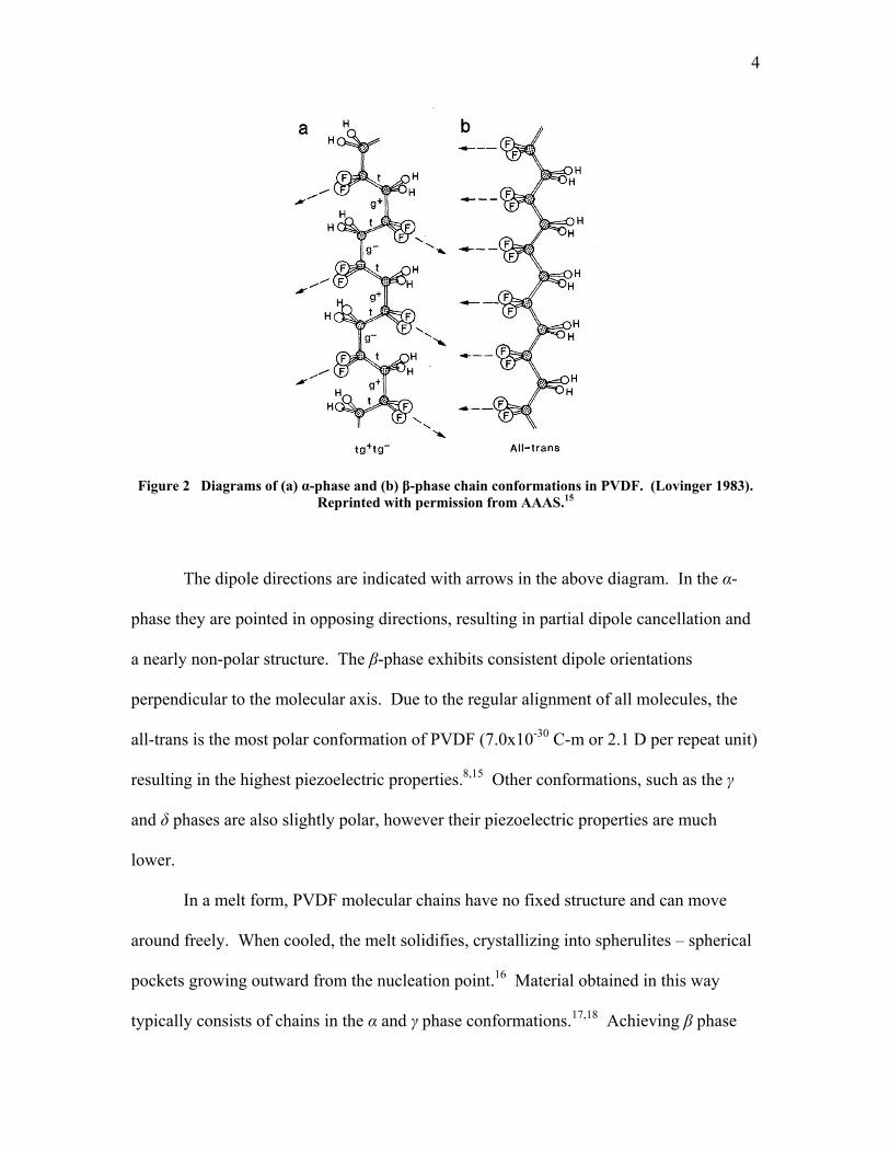
Figure 2 Diagrams of (a) α-phase and (b) β-phase chain conformations in PVDF. (Lovinger 1983). Reprinted with permission from AAAS.15
The dipole directions are indicated with arrows in the above diagram. In the α-
phase they are pointed in opposing directions, resulting in partial dipole cancellation and
a nearly non-polar structure. The β-phase exhibits consistent dipole orientations
perpendicular to the molecular axis. Due to the regular alignment of all molecules, the
all-trans is the most polar conformation of PVDF (7.0x10⁻³⁰ C-m or 2.1 D per repeat unit)
resulting in the highest piezoelectric properties.8,15 Other conformations, such as the γ
and δ phases are also slightly polar, however their piezoelectric properties are much
lower.
In a melt form, PVDF molecular chains have no fixed structure and can move
around freely. When cooled, the melt solidifies, crystallizing into spherulites – spherical
pockets growing outward from the nucleation point.16 Material obtained in this way
typically consists of chains in the α and γ phase conformations.17,18 Achieving β phase
5
structures normally requires additional processing as discussed later in the manufacturing
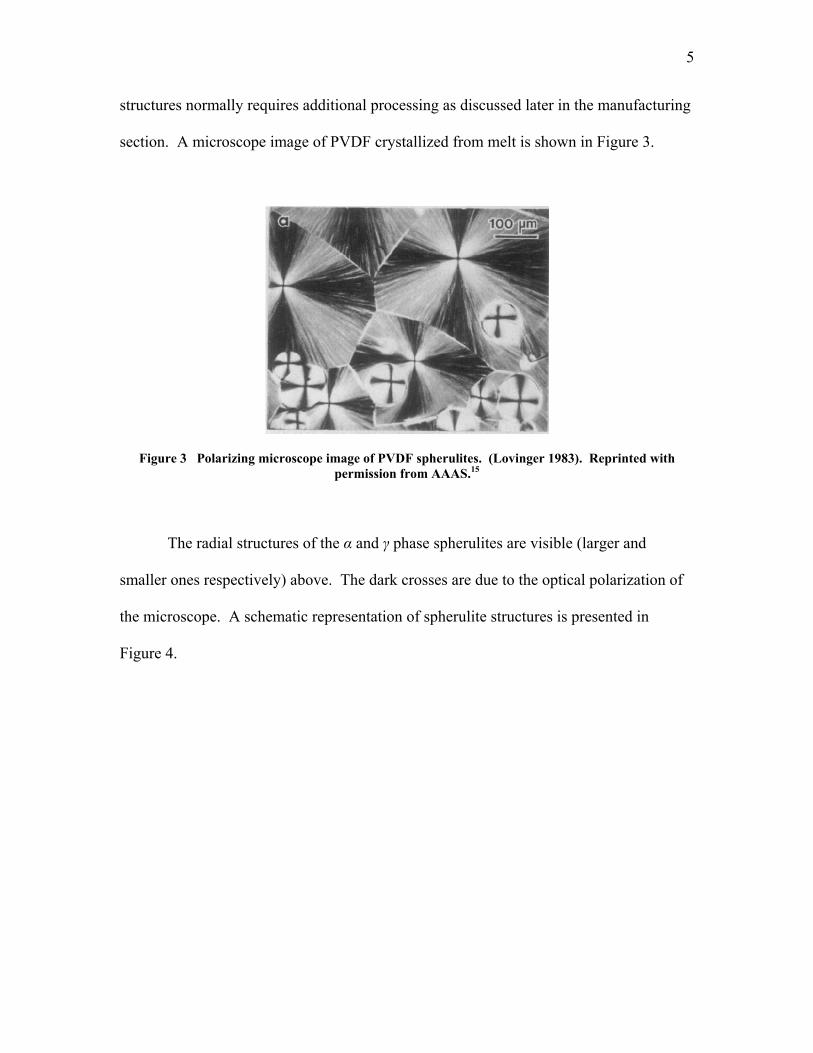
section. A microscope image of PVDF crystallized from melt is shown in Figure 3.
Figure 3 Polarizing microscope image of PVDF spherulites. (Lovinger 1983). Reprinted with permission from AAAS.15
The radial structures of the α and γ phase spherulites are visible (larger and
smaller ones respectively) above. The dark crosses are due to the optical polarization of
the microscope. A schematic representation of spherulite structures is presented in
Figure 4.

6
Figure 4 PVDF spherulite structure diagram.7
PVDF never crystallizes completely and as shown in this diagram both crystalline
lamella structures and amorphous regions are present. The radial fibers, also visible in an
earlier microscope image (Figure 3) consist of very thin, platelet-like crystals called
lamellae separated by amorphous regions. The lamellae are segments of polymer chains
packed in a crystalline order. They are on the order of a few nanometers thick and
several micrometers in lateral dimensions.8,15 The lamellae are surrounded by an
amorphous structure also known as supercooled liquid phase due to its physical
properties. Each PVDF molecule normally extends through several crystalline and
amorphous regions. This two-phase solid state structure is typical of crystallizable
polymers.15
The degree of crystallinity in PVDF ranges within 50-65% according to specific
volume calculations.19 This value varies slightly depending on material thermal history
and the amount of chain ordering defects.20 Chain defects are head-to-head (CH2
followed by CH2), and tail-to-tail (CF2 followed by CF2) bonds which occur during
7
polymerization. They are found in less than five percent of the sequences as shown by
nuclear magnetic resonance spectroscopy studies.15
Due to physical characteristics of the material, piezoelectric properties are limited
to certain temperature ranges. They vanish temporarily below the PVDF glass
temperature Tg (- 40°C). Also, when temperature rises beyond the Curie temperature Tc
(80°C) the piezoelectric properties are lost permanently due to structural changes in the
material.21
I.3 Piezoelectric behavior overview
PVDF belongs to a group of piezoelectric materials which also display an
additional property known as pyroelectricity. It is the ability to generate an electrical
charge with temperature change. This behavior is due to the permanently polar structure
of the material. In addition to being polar, some pyroelectric materials can have their
spontaneous polarization axis reoriented or reversed with the application of an electric
field. These materials are referred to as ferroelectric.15 The name is derived by analogy
with ferromagnetism, where the individual atoms exhibit permanent magnetic
moments.22,23
It was initially uncertain whether PVDF is truly ferroelectric. Studies have shown
inhomogeneous polarization across the film thickness, with higher polarization on the
positive electrode charge. This lead to speculations that the PVDF properties were due to
trapped charges injected by the electrodes.23,24 The dilemma was resolved when X-ray
studies showed that polarization anisotropy disappears at high poling fields, and that
ferroelectric dipole reorientation can be achieved.25 Polarization reversal was further

8
attributed to dipole rotation using infrared techniques.26 Typical ferroelectric hysterisis
loops and Curie transitions were also shown to exist in this material.15 PVDF is therefore
considered to be a ferroelectric polymer.
There remains some uncertainty about the basic mechanism responsible for
piezoelectricity in PVDF. Given its semi-crystalline structure, PVDF is modeled as a
two-phase matrix with varied properties.7,27 Piezoelectric response is dependent on
polarization (average dipole moment per unit volume), which can be affected by changes
in either dipole moment or volume.7 A diagram in Figure 5 shows crystalline lamellar
structure of PVDF.
Figure 5 Diagram of a PVDF lamellar crystal and its dipole orientation.7
The dipole moment md and its angle θ0 in relation to direction normal to the
surface are shown for reference. The material’s polarization and piezoelectric response
are therefore affected by density of crystals (and hence crystallinity)28 and their mean
orientation.
9
As summarized by Broadhurst and Davis,6 there are four essential elements to
piezoelectricity: (a) the presence of permanent molecular dipoles; (b) the ability to orient
or align the molecular dipoles; (c) the ability to sustain the dipole alignment achieved;
and (d) the ability of the material to undergo large strains when mechanically stressed.
I.4 Piezoelectric mechanism research
A number of different approaches for explaining the piezoelectric effect have
been explored over the years. After an initial debate regarding the influence of trapped
space charges, scientists now agree that while space charges do attribute to the material’s
properties, their effect is negligible as over 90% of piezoelectric response occurs due to
polarization of dipoles in crystalline areas.8,28,29
Some researchers propose that due to the dipole alignment and high
compressibility of PVDF, large polarization changes can occur through changes in
volume,4,30,31 especially through thickness changes (also known as dimensional effect).28
Other theoretical mechanisms are based on changes in moment, including Ohigashi’s
proposed dipole alignment increase due to mechanical stress.32 Most studies agree that
PVDF should be modeled as a two-phase matrix of crystalline and amorphous phases
with different mechanical and dielectric properties.7,33,34 It is then believed that the
piezoelectric effect is due to mechanical and electrical interaction between crystalline and
amorphous phases.27 The specific examples of piezoelectricity sources in two-phase
materials can be explained as follows:34
(a) The intrinsic piezoelectricity of crystalline elements creates the
piezoelectricity due to the strain dependence of the polarization (crystal contribution).

10
(b) The relationship between the dielectric constants and strain is different
between the crystalline and amorphous phases. With the presence of polarization these
differences add to the piezoelectric effect in the material (electrostrictive contribution).
(c) The elastic constants of the crystalline and amorphous regions are also
different. In a polarized sample, the resulting strain dependence of the polarization
contributes to the piezoelectric activity (dimensional contribution).
This concludes the overview of existing studies of piezoelectricity in PVDF. The
following section presents the general mathematical formulations used to describe this
phenomenon.
I.5 General piezoelectric equations
Piezoelectricity is a coupling mechanism relating material’s mechanical and
electrical properties, as outlined in Figure 6.

11
Figure 6 Relationships among material properties.35
Constitutive relations describing the piezoelectric behavior in materials can be
derived from thermodynamic principles.36 A tensor notation is normally used to identify
the coupling mechanisms. It is common practice to label the axis directions as shown in
Figure 7.

12
Figure 7 Tensor directions for constitutive relation definitions.
The mechanical drawing direction is labeled as "l". The "2" axis is the transverse
direction in the plane of the sheet. The polarization axis (normal to film surface) is
denoted as "3". Additional shear planes indicated by subscripts "4", "5", "6" are defined
perpendicular to directions "l", "2", and "3" respectively.23
Piezoelectricity can be described by four constants dij, eij, gij, and hij. These
constants relate elastic coefficients (mechanical stress T and strain S) and dielectric
variables (electric displacement D and electric field E). The relationships are defined by
the following formulas:28
E T
i iij
j j
D SdT E
⎛ ⎞ ⎛ ⎞∂ ∂= =⎜ ⎟ ⎜ ⎟⎜ ⎟ ⎜ ⎟∂ ∂⎝ ⎠ ⎝ ⎠
(1.1)
E S
i iij
j j
D TeS E
⎛ ⎞ ⎛ ⎞∂ ∂= = −⎜ ⎟ ⎜ ⎟⎜ ⎟ ⎜ ⎟∂ ∂⎝ ⎠ ⎝ ⎠
(1.2)
1
3
2
Drawing direction
Poling direction

13
D T
i iij
j j
E SgT D
⎛ ⎞ ⎛ ⎞∂ ∂= − =⎜ ⎟ ⎜ ⎟⎜ ⎟ ⎜ ⎟∂ ∂⎝ ⎠ ⎝ ⎠
(1.3)
D S
i iij
j j
E ThS D
⎛ ⎞ ⎛ ⎞∂ ∂= =⎜ ⎟ ⎜ ⎟⎜ ⎟ ⎜ ⎟∂ ∂⎝ ⎠ ⎝ ⎠
(1.4)
The first two equations (1.1, 1.2) correspond to the direct piezoelectric effect,
while the last two (1.3, 1.4) refer to the inverse piezoelectric effect. The superscripts
describe the experimental conditions: E denotes zero electric field (a closed circuit), D
stands for zero electric induction (an open circuit), T corresponds to zero mechanical
stress (a free sample), and S indicates zero strain (a fixed sample). The subscripts are i =
1–3 and j = 1–6. The above piezoelectric constants are related to each other through the
elastic constant (c) and dielectric constant (ε), can be calculated as:23,28
gh
dec == (1.5)
he
gd==0εε (1.6)
where ε0 = 8.854x10⁻¹² (F/m) is the permittivity of vacuum. The permittivity of
piezoelectric materials depends on the boundary conditions. The free (dT = 0)
permittivity εT is always larger than the clamped (dS=0) permittivity εS because a free
sample piezoelectric generates additional polarization due to converse and direct piezo
effects. Similarly, the open-circuit (dD=0) elastic constant cD is larger than the short-
circuit (dE=0) constant cE. The above dependences define the electromechanical
coupling coefficient k as:23,28
21S E
T D
c kc
εε
= = − (1.7)
14
where k2, which is always less than 1, represents the conversion of electrical
energy into mechanical energy and vice versa due to piezoelectricity.
2
2
electrical energy converted to mechanical energykinput electrical energy
mechanical energy converted to electrical energykinput mechanical energy
=
= (1.8)
The focus of this application is on linear piezoelectricity, which is described in the
following section.
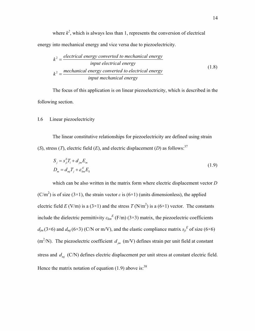
I.6 Linear piezoelectricity
The linear constitutive relationships for piezoelectricity are defined using strain
(S), stress (T), electric field (E), and electric displacement (D) as follows:37
Ej ji i jm m
Em mj j km k
S s T d E
D d T Eε
= +
= + (1.9)
which can be also written in the matrix form where electric displacement vector D
(C/m2) is of size (3×1), the strain vector ε is (6×1) (units dimensionless), the applied
electric field E (V/m) is a (3×1) and the stress T (N/m2) is a (6×1) vector. The constants
include the dielectric permittivity εkmE (F/m) (3×3) matrix, the piezoelectric coefficients
djm (3×6) and dmj (6×3) (C/N or m/V), and the elastic compliance matrix sjiE of size (6×6)
(m2/N). The piezoelectric coefficient jmd (m/V) defines strain per unit field at constant
stress and mjd (C/N) defines electric displacement per unit stress at constant electric field.
Hence the matrix notation of equation (1.9) above is:38
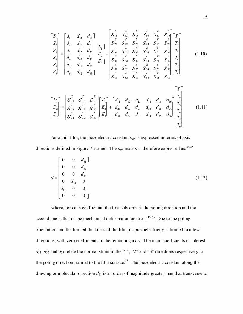
15
11 12 13 14 15 161 11 12 13
21 22 23 24 25 262 21 22 231
3 31 32 33 31 32 33 34 35 362
4 41 42 43 413
5 51 52 53
6 61 62 63
E E E E E E
E E E E E E
E E E E E E
E
S d d dS d d d
ES d d d
ES d d d
ES d d dS d d d
s s s s s ss s s s s ss s s s s ss
⎡ ⎤ ⎡ ⎤⎢ ⎥ ⎢ ⎥⎢ ⎥ ⎢ ⎥ ⎡ ⎤⎢ ⎥ ⎢ ⎥ ⎢ ⎥= +⎢ ⎥ ⎢ ⎥ ⎢ ⎥⎢ ⎥ ⎢ ⎥ ⎢ ⎥⎣ ⎦⎢ ⎥ ⎢ ⎥⎢ ⎥ ⎢ ⎥⎢ ⎥ ⎢ ⎥⎣ ⎦ ⎣ ⎦
1
2
3
442 43 44 45 46
551 52 53 54 55 56
661 62 63 64 65 66
E E E E E
E E E E E E
E E E E E E
TTTTTT
s s s s ss s s s s ss s s s s s
⎡ ⎤⎡ ⎤⎢ ⎥⎢ ⎥⎢ ⎥⎢ ⎥⎢ ⎥⎢ ⎥⎢ ⎥⎢ ⎥⎢ ⎥⎢ ⎥⎢ ⎥⎢ ⎥⎢ ⎥⎢ ⎥⎢ ⎥⎢ ⎥⎣ ⎦⎢ ⎥
⎣ ⎦
(1.10)
1
211 12 131 1 11 12 13 14 15 16
32 2 21 22 23 24 25 2621 22 23
43 3 31 32 33 34 35 36
31 32 33 5
6
T T T
T T T
T T T
TT
D E d d d d d dT
D E d d d d d dT
D E d d d d d dTT
ε ε εε ε εε ε ε
⎡ ⎤⎢ ⎥
⎡ ⎤ ⎢ ⎥⎡ ⎤ ⎡ ⎤ ⎡ ⎤⎢ ⎥ ⎢ ⎥⎢ ⎥ ⎢ ⎥ ⎢ ⎥⎢ ⎥= + ⎢ ⎥⎢ ⎥ ⎢ ⎥ ⎢ ⎥⎢ ⎥ ⎢ ⎥⎢ ⎥ ⎢ ⎥ ⎢ ⎥⎣ ⎦ ⎣ ⎦ ⎣ ⎦⎢ ⎥ ⎢ ⎥⎣ ⎦⎢ ⎥⎢ ⎥⎣ ⎦
(1.11)
For a thin film, the piezoelectric constant djm is expressed in terms of axis
directions defined in Figure 7 earlier. The djm matrix is therefore expressed as:23,38
31
32
33
24
15
0 00 00 00 0
0 00 0 0
ddd
dd
d
⎡ ⎤⎢ ⎥⎢ ⎥⎢ ⎥
= ⎢ ⎥⎢ ⎥⎢ ⎥⎢ ⎥⎣ ⎦
(1.12)
where, for each coefficient, the first subscript is the poling direction and the
second one is that of the mechanical deformation or stress.15,23 Due to the poling
orientation and the limited thickness of the film, its piezoelectricity is limited to a few
directions, with zero coefficients in the remaining axis. The main coefficients of interest
d31, d32 and d33 relate the normal strain in the “1”, “2” and “3” directions respectively to
the poling direction normal to the film surface.38 The piezoelectric constant along the
drawing or molecular direction d31 is an order of magnitude greater than that transverse to

16
the polymer chains d32. Both are positive, since stress in the film plane reduces the
specimen thickness, thus increasing the surface charge. The d33 coefficient is negative
because a stress normal to the film increases its thickness.15 Additional coefficients d15
and d24 represent the shear strain in the 1-3 plane and the 2-3 plane respectively.38 They
arise from anisotropy due to texturing created by mechanical elongation during material
processing.28,38,39,40,41 Individual piezoelectric constants can be determined through
resonance studies using direct and converse effects, or calculated if other piezoelectric
constants are already known.23,28,42 For most sensor applications, the d31 (transverse
effect) and d33 (longitudinal effect) components are of primary importance.28
In this research, the electrical charge generation due to mechanical deflection is
studied experimentally. Charge build-up is normally only seen while deflection is
changing. In a static condition, it dissipates through the PVDF film and the measuring
equipment. A simplification is made for the purpose of further mathematical analysis of
this study. Since it is not possible to analyze piezoelectric materials in purely static
conditions due to coupling between electrical and dynamic mechanical variables, quasi-
static conditions are considered instead. This is possible, because full electromagnetic
equations can be neglected in the piezoelectric behavior considerations, as the magnetic
effects are known to be significantly smaller than the electrical effects.37 In addition, the
external applied electric field E is zero, simplifying the piezo relations further.
Therefore, the relevant piezoelectric equation becomes:
m mj jD d T= (1.13)
or in the matrix form:38

17
1
21 15 16
32 24
43 31 32 33
5
6
0 0 0 00 0 0 0 0
0 0 0
TT
D d dT
D dT
D d d dTT
⎡ ⎤⎢ ⎥⎢ ⎥⎡ ⎤ ⎡ ⎤⎢ ⎥⎢ ⎥ ⎢ ⎥= ⎢ ⎥⎢ ⎥ ⎢ ⎥⎢ ⎥⎢ ⎥ ⎢ ⎥⎣ ⎦ ⎣ ⎦ ⎢ ⎥⎢ ⎥⎢ ⎥⎣ ⎦
(1.14)
where the stress vector is defined as:
1 11
2 22
3 33
4 23
5 31
6 12
T TT TT TT TT TT T
⎡ ⎤ ⎡ ⎤⎢ ⎥ ⎢ ⎥⎢ ⎥ ⎢ ⎥⎢ ⎥ ⎢ ⎥
=⎢ ⎥ ⎢ ⎥⎢ ⎥ ⎢ ⎥⎢ ⎥ ⎢ ⎥⎢ ⎥ ⎢ ⎥
⎢ ⎥⎢ ⎥ ⎣ ⎦⎣ ⎦
(1.15)
The electric displacement D is related to the charge generated by the following
relation:38
[ ]1
1 2 3 2
3
dAq D D D dA
dA
⎡ ⎤⎢ ⎥= ⎢ ⎥⎢ ⎥⎣ ⎦
∫∫ (1.16)
where dA1, dA2 and dA3 are the components of the electrode area in the 2-3, 1-3
and 1-2 planes respectively. Therefore, the generated charge q depends only on the
component of the displacement D normal to the electrode area dA.38 It is worth noting
that a pair of parallel electrodes is needed to measure piezoelectric charge. If shaped
electrodes are used on each side of the film, dA consists only of the area where electrodes
overlap.21 This concludes the summary of the piezoelectric effect for this study.
18
I.7 Manufacturing processes
This section presents an overview of the manufacturing process for the
piezoelectric PVDF. The polymer can be synthesized from gaseous vinylidene fluoride
(VDF) monomer through a free radical polymerization. It can be then formed into sheets
through melt casting, or processing from a solution (e.g. solution casting, spin coating,
and film casting). Depending on the processing method, various chain conformations of
PVDF films may result.8,43,44 Additional steps are necessary to obtain the piezoelectric
properties within the material. Most common manufacturing techniques start with a slow
melt casting process, resulting in an α phase material. Additional steps are then taken to
achieve the desired piezoelectric properties. Step-by-step methods are presented Figure 8.
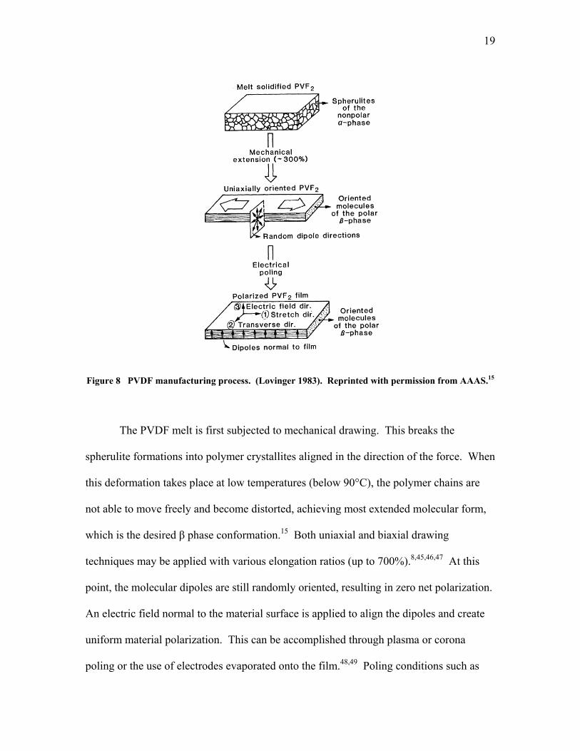
19
Figure 8 PVDF manufacturing process. (Lovinger 1983). Reprinted with permission from AAAS.15
The PVDF melt is first subjected to mechanical drawing. This breaks the
spherulite formations into polymer crystallites aligned in the direction of the force. When
this deformation takes place at low temperatures (below 90°C), the polymer chains are
not able to move freely and become distorted, achieving most extended molecular form,
which is the desired β phase conformation.15 Both uniaxial and biaxial drawing
techniques may be applied with various elongation ratios (up to 700%).8,45,46,47 At this
point, the molecular dipoles are still randomly oriented, resulting in zero net polarization.
An electric field normal to the material surface is applied to align the dipoles and create
uniform material polarization. This can be accomplished through plasma or corona
poling or the use of electrodes evaporated onto the film.48,49 Poling conditions such as
20
field strength, temperature and poling time can vary, although increased values don’t
necessarily guarantee higher resulting piezoelectricity.28 This completes the process and
gives PVDF piezoelectric properties, making into a useful electroactive polymer.
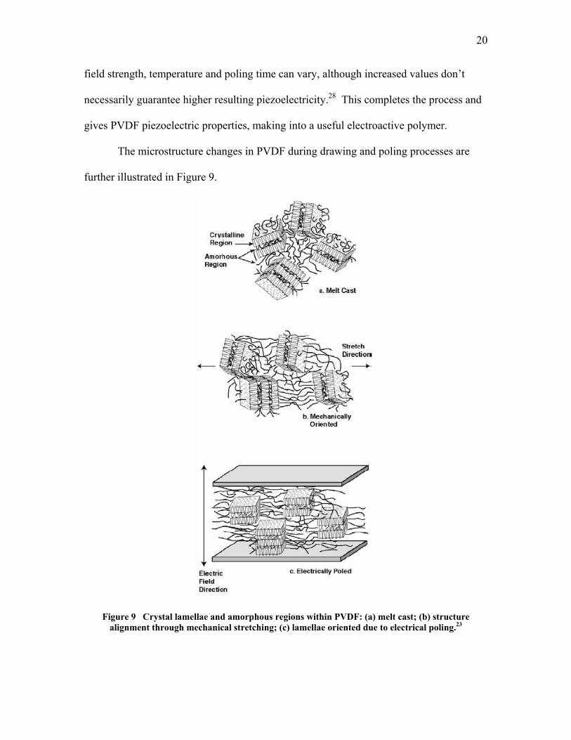
The microstructure changes in PVDF during drawing and poling processes are
further illustrated in Figure 9.
Figure 9 Crystal lamellae and amorphous regions within PVDF: (a) melt cast; (b) structure alignment through mechanical stretching; (c) lamellae oriented due to electrical poling.23

21
Figure 9(a) shows the randomly oriented crystalline and amorphous structures
found in the polymer melt. Mechanical drawing extends the crystals into the polar β
phase conformation and orients them as shown in Figure 9(b). Finally, through electrical
poling the crystalline lamellae are aligned in a single direction as shown in Figure 9(c),
resulting in a uniformly polar material with piezoelectric properties.
There are a number of other polymers that can be made piezoelectric,35 however
PVDF exhibits by far the strongest piezoelectric and pyroelectric properties.15 As
described earlier, the piezoelectric properties are dependent on its molecular form, level
of crystallinity and the poling process. Since the discovery of piezoelectricity in PVDF
in 1969, its piezoelectric constants have increased about six times due to process
advancements. Further progress can be expected, however dramatic future improvements
are not likely.8
I.8 Applications
Polyvinylidene fluoride is a well known commercial material with many useful
characteristics and a wide range of applications. Some of its most important properties
include: high purity, resistance to weather and chemicals, light weight, mechanical
strength and abrasion resistance. It’s thermoplastic and can be easily processed into
various shapes. Non-piezoelectric PVDF, marketed as Kynar®, finds uses in pipes and
chemical storage tanks, coating and paint additives, electrical wire jacketing, battery
components and other products.50
Piezoelectric PVDF is commonly used for sensors, actuators and transducers. Its
key benefits in these applications include: high voltage sensitivity, flexibility, toughness
22
and manufacturability. It can be made biocompatible and its low acoustic impedance is
close to that of water, making it useful for fluid sensors and biomedical applications.23,51
An full list of commercial and research applications includes: strain and strain rate
gauges21; potential active biomedical materials52,53; switches, impact and vibrations
sensors, accelerometers54,55; flow detectors47; devices in acoustics, ultrasonics and
vibration control.54,56,57,58 In summary, piezoelectric PVDF has many uses in sensing and
actuating applications. In this study, it is utilized as a deflection sensor. The application
details are discussed in the following section.
I.9 Motivation and objectives
A detailed introduction to piezoelectric materials has been presented in previous
sections to provide a solid background of the topic. This research focuses on the use of
PVDF as a deflection sensor to monitor small insects, such as cockroaches. Using
piezoelectric polymers to study insects has significant importance in the fields of biology,
engineering, and science. This research uses an experimental approach combined with
simple analytical techniques to develop, test, and optimize PVDF sensors for monitoring
cockroaches.
For decades, understanding and mimicking insect locomotion has been the focus
of numerous studies.59,60 The goal has often been learning about the connection between
muscle activity and movement, leading to the development of motion simulations and
models.61,62,63,64 Another popular area of research is animal monitoring. A wide variety
of technological devices have been developed to observe and study insects remotely
without direct interference.65 This area of research, known as “wildlife telemetry” has

23
gained additional momentum through miniaturization of data transfer devices for the use
with small animals and insects.66,67,68,69,70 Roaches in particular have been an interest of
many studies, because they are common and inherently related to people and their
environments.
For this research a discoid roach, Blaberus discoidalis is used. It is a neotropical
species that is easy to rear and useful as a biological insect model. The roaches, shown in
Figure 10, are about 40 mm long, which makes them relatively easy to handle.
Figure 10 Discoid roach (Blaberus discoidalis) – relative size (L-female, R-male).71
Roaches are found almost every place where there is food and moisture.72,73,74
They are omnivorous, preferring to sweets but also found eating a variety of commercial
and household foods and materials.62,65 There are several reasons to study the Blaberus
discoidalis. This species, as any other roach, has a simple biological structure are easy to
obtain and maintain. Long-term monitoring of roaches’ behavior and their appetite
allows the analysis of their food structure and agriculture distribution, which have a
significant impact on environmental studies.
24
I.10 Approaches
An experimental approach was taken for the initial phase of the project focused
on developing miniature, robust sensors and dependable testing platforms for both
laboratory and roach experiments. Results of initial tests, along with basic analytical
considerations, were used to improve the performance and reliability of the sensors and
the testing setups. Experiments were then carried out to characterize the relationship
between the cockroach movements and the sensor response to further the understanding
of insect behavior.
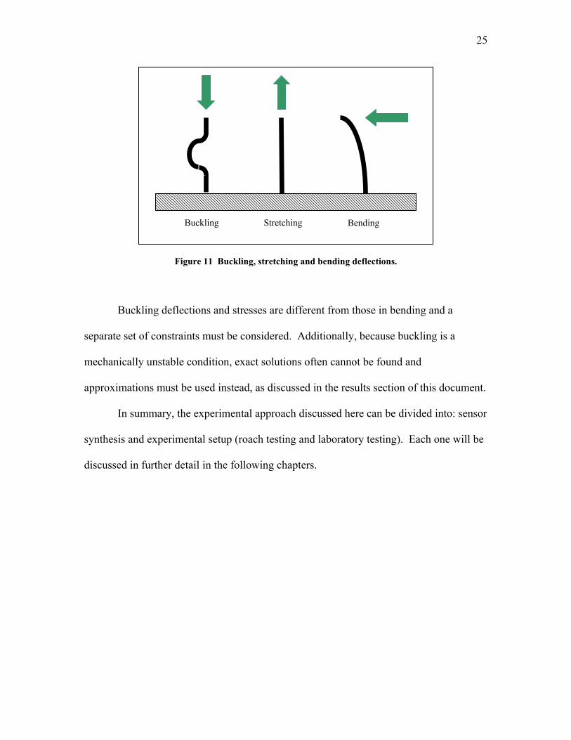
This research presents a set of interesting engineering challenges. The main
difficulty is the miniature size of the application, which limits the techniques available for
sensor synthesis and mounting. The process of selecting a sensor attachment method has
shown that the most reliable approach results in the piezoelectric film undergoing a
buckling deformation during insect movement. While PVDF film has been studied
extensively, most of the research to date focused on its behavior in stretching or bending
applications. The difference between them is shown in Figure 11.
25
Figure 11 Buckling, stretching and bending deflections.
Buckling deflections and stresses are different from those in bending and a
separate set of constraints must be considered. Additionally, because buckling is a
mechanically unstable condition, exact solutions often cannot be found and
approximations must be used instead, as discussed in the results section of this document.
In summary, the experimental approach discussed here can be divided into: sensor
synthesis and experimental setup (roach testing and laboratory testing). Each one will be
discussed in further detail in the following chapters.
Stretching Bending Buckling
26
CHAPTER II
SENSOR FABRICATION
This section presents a brief overview of the materials used, their preparation,
assembly and implementation in the presented study.
II.1 Materials
Metallized piezoelectric film (Measurement Specialties, part number 1-1004346-
1) was used for this study. It consists of a 28µm layer of PVDF with coatings of silver
ink deposited on both sides (5-7 µm each) to provide an electrical connection. Thin,
insulated copper wires, 0.0047” (0.12 mm) in diameter, were used for electrical leads.
Standard semi-clear adhesive scotch tape was used to assemble the sensors. Tools such
as fine sandpaper (320 grain) for removing wire insulation, and scalpel blades for cutting
sensor material were also used in the project.
II.2 Material properties
A summary of PVDF film characteristics, as provided by the manufacturer, are
listed in Table 1:
27
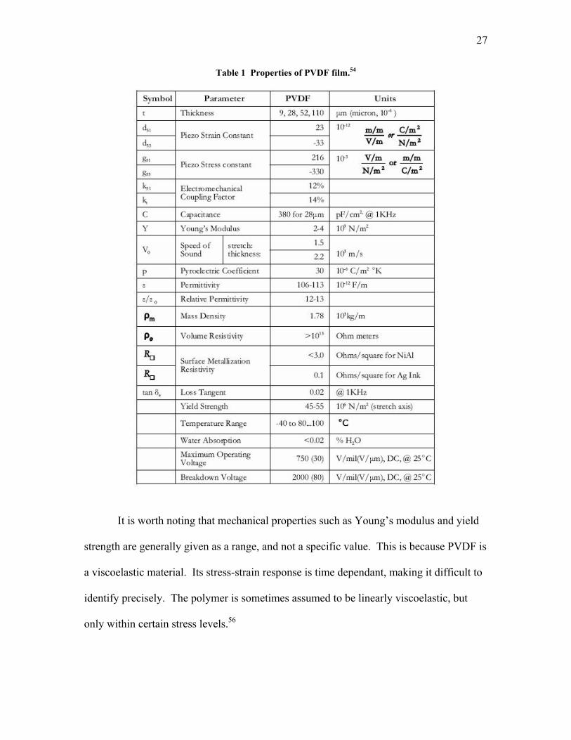
Table 1 Properties of PVDF film.54
It is worth noting that mechanical properties such as Young’s modulus and yield
strength are generally given as a range, and not a specific value. This is because PVDF is
a viscoelastic material. Its stress-strain response is time dependant, making it difficult to
identify precisely. The polymer is sometimes assumed to be linearly viscoelastic, but
only within certain stress levels.56

28
II.3 Sensor synthesis
For the purpose of this work, commercially available thin piezoelectric PVDF
film was used. The material is available from Measurement Specialties in various
thicknesses (28, 52 and 110 µm). It is made using techniques similar to those described
earlier in the manufacturing section (I.7). The piezoelectric film is then metallized
through a process described in the next section. The application requires the sensors to
be flexible and robust at the same time. After initial testing, the 28 µm PVDF was
chosen, because it provides little or no interference with the insects’ movements. Its
drawback is that it is easier to damage and its output signal is lower than that of thicker
films. Complete details of sensor preparation are discussed in the following sections.
II.3.1 Metallization
For PVDF to be used as a sensor, a thin metal layer is deposited on each side of
the film. This creates two electrodes and allows for measurement of the charge
generated. Possible methods include screen printing with conductive silver ink. The
resulting metallization layer is fairly thick (5-7 µm). This provides additional strength
and improved durability, making the film more useful for mechanical applications. Silver
ink metallization also provides good quality of the surface finish. It has a flat grey color
and low reflectivity. A laser light used to measure sensor lateral deflection (as discussed
in later chapters) doesn’t reflect or scatter on this surface easily, allowing for more
consistent readings.
Additional coating techniques are used including sputtering metallization, which
results in thinner coating layers. Various metals and alloys can be deposited at a
thickness around 500-700 Å. While this allows the film to be more flexible, the
29
metallization layer is not as robust and tends to crack due to repeated deformations.
Also, the surface is highly reflective, making it a less reliable target for the laser distance
gauge.54,75
II.3.2 Sensor preparation
Sensors are cut from PVDF film using a razor blade. Care must be taken not to
stretch the material while cutting it. If the film becomes distorted, its two surface layers
may come in contact, creating an electrical connection between them and making the
sensor useless. Repeatable sensor sizes may also be difficult to achieve with a manual
cutting process. Alternate, more reliable methods have been explored, such as custom
punches to cut the piezoelectric film.76 They may become useful in the future
development of the project.
II.3.3 Lead attachment methods
Wire leads are critical to the sensor operation, allowing the measurement of the
generated signal. Thin 0.0047” (0.12 mm) copper wires with flexible electrical insulation
are used. Insulation prevents accidental electrical “shorting” between the leads and is
removed at the connection points with the sensor. Insulation removal can be challenging
due to the small wire size. The most reliable solution found so far has been using fine
sandpaper (320 grain) to remove the coating.
A number of wire attachment methods have been considered. Commercial
solutions, such as penetrative techniques (piercing, riveting, crimping, etc) are not
possible due to the miniature sensor dimensions and the need for patterned lead-off
electrodes. The application and reliability of non-penetrative methods (low temperature
soldering, conductive epoxies and adhesives) are also limited due to the sensor size.54
30
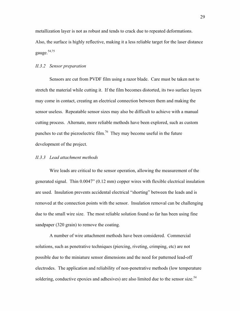
Simple wire attachments with adhesive scotch tape shown in Figure 12 have been found
to be most effective. They are easy to implement and durable enough to meet the
operating requirements of the sensor.
Figure 12 Detailed sensor schematic.
To provide a good electrical connection, wire insulation is removed over a length
of about two millimeters from the end of each wire using sandpaper. The exposed leads
are placed on each side of the sensor, slightly apart to avoid a possible connection
between them. The sensor and wire leads are then “sandwiched” together between the
two layers of tape as shown above. The wire attachment area is about 2 mm long and 1
LEGEND:
Sensor top view Detailed side view
Metallized PVDF material
Adhesive tape
Lead wires (one on each side)
PVDF material
Silver ink metallization
Wire leads
Adhesive tape
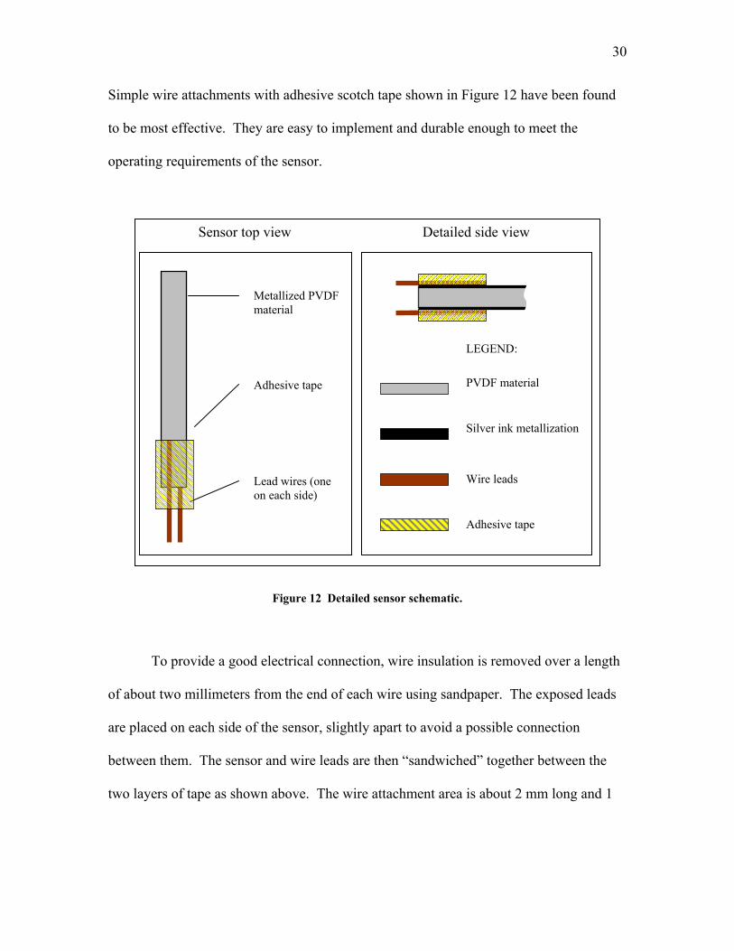
31
mm across. The sensor itself is 10 mm long and 1 mm wide. An image of a complete
sensor with a scale for size reference is shown in Figure 13.
Figure 13 Image of a complete sensor.
The wires and their attachment points are limited in strength and easy to damage.
The forces generated by insects are very small and it has been found that the sensors are
fairly durable if handled with care. Possible improvements may be considered in later
stages of the project.
II.4 Sensor mounting
The completed PVDF sensors were mounted on insects’ legs to monitor their
movements by measuring the generated charge. The piezoelectric sensor was attached to
one of the metathoracic (rear) leg. Since those are the largest legs, they are easiest for
sensor mounting, and also likely to generate highest forces and deflections. The
attachment points are across the leg joints, one between the coxa and the femur (C-F),
and another between the femur and the tibia (F-T) as shown in Figure 14.
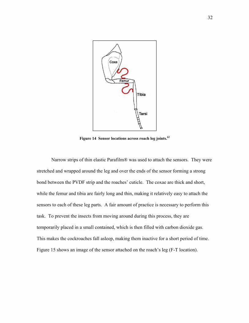
32
Figure 14 Sensor locations across roach leg joints.62
Narrow strips of thin elastic Parafilm® was used to attach the sensors. They were
stretched and wrapped around the leg and over the ends of the sensor forming a strong
bond between the PVDF strip and the roaches’ cuticle. The coxae are thick and short,
while the femur and tibia are fairly long and thin, making it relatively easy to attach the
sensors to each of these leg parts. A fair amount of practice is necessary to perform this
task. To prevent the insects from moving around during this process, they are
temporarily placed in a small contained, which is then filled with carbon dioxide gas.
This makes the cockroaches fall asleep, making them inactive for a short period of time.
Figure 15 shows an image of the sensor attached on the roach’s leg (F-T location).

33
Figure 15 Scanning electrode microscope (SEM) image of roach leg with a sensor.77
The sensor is thereby fixed to the leg with enough flexibility to deflect during
insects’ movements. The charge generated due to the film’s piezoelectric properties can
be measured and analyzed further. Details of the testing equipment and the experimental
setup are presented in the next chapter.
.
Parafilm strips
PVDF sensor

34
CHAPTER III
EXPERIMENTAL SETUP
The experiments performed in this study can be grouped into sensor tests and
material microstructure studies. Sensor experiment setups can be further divided into
insect testing system and laboratory system.
III.1 Sensor testing background
Because the insect is a complex testing platform with limited control, it is useful
to first develop a good understanding of sensor performance through studies in controlled
environment, before trying to analyze data gathered from a live cockroach. It is
important for the laboratory experimental setup to maintain similar mounting and
operating characteristics found in the roach application. As discussed earlier in section
I.10, the sensor deformation can be defined as buckling. This is further illustrated in
Figure 16(a). The laboratory setup has the capability of creating similar sensor
deflections, shown in Figure 16(b), under repeatable and precisely defined conditions.

35
Figure 16 Side-view schematic of sensor mounting and deformations – arrows indicate motion directions.
In the experimental setup, the left mounting block is stationary, while the right
one moves in the horizontal direction as shown by an arrow. The sensor buckling rate
and deflection amplitude are directly controlled by the position of the movable fixture.
Various motion paths can be defined, allowing the flexibility to generate various
operating conditions. Simple motions can be implemented for studying the basic
characteristics of the sensor. More complex deformations can be used to mimic real
applications. Operating conditions of a sensor on an insect likely consist of a series of
deflections, possibly of different amplitudes, occurring through across a range of
frequencies. The roach is reported to be able to maintain sustained speeds at a rate up to
13 Hz.78 Experiments performed so far were focused on lower deflection rates (below 10
Hz) to gain the basic understanding of the sensor and its operation. However, the
Laboratory setup Roach leg application
Leg joint extended (sensor neutral position)
Leg joint flexed (sensor under buckling)
Testing condition (sensor under buckling)
Sensor mounting (sensor neutral position)
36
experimental system is capable of reaching the maximum frequencies expected during
the roach motion.
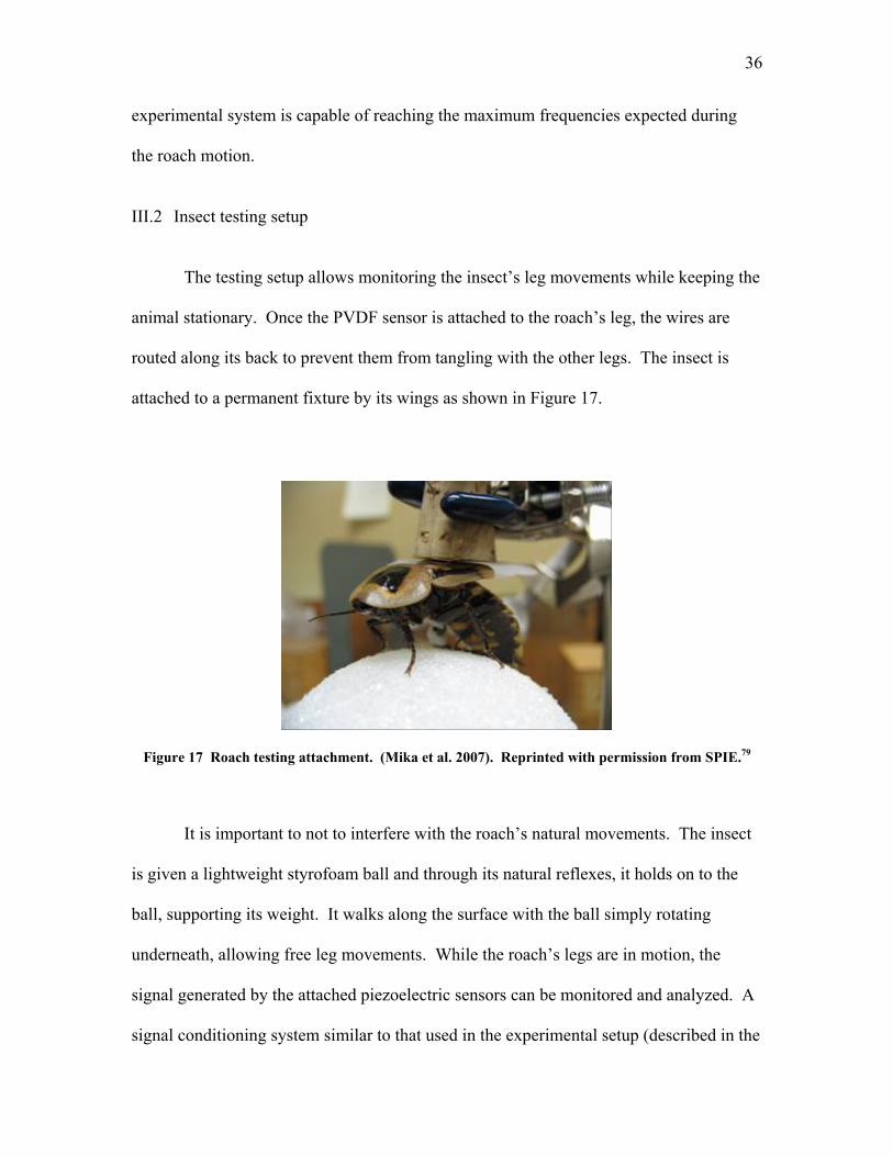
III.2 Insect testing setup
The testing setup allows monitoring the insect’s leg movements while keeping the
animal stationary. Once the PVDF sensor is attached to the roach’s leg, the wires are
routed along its back to prevent them from tangling with the other legs. The insect is
attached to a permanent fixture by its wings as shown in Figure 17.
Figure 17 Roach testing attachment. (Mika et al. 2007). Reprinted with permission from SPIE.79
It is important to not to interfere with the roach’s natural movements. The insect
is given a lightweight styrofoam ball and through its natural reflexes, it holds on to the
ball, supporting its weight. It walks along the surface with the ball simply rotating
underneath, allowing free leg movements. While the roach’s legs are in motion, the
signal generated by the attached piezoelectric sensors can be monitored and analyzed. A
signal conditioning system similar to that used in the experimental setup (described in the
37
next section) is used. It uses the same charge amplification setup, while the data is
recorded through a portable oscilloscope (Tektronix, model THS720P) and transferred to
a computer. Current improvement efforts are focused on replacing this data gathering
setup and utilizing computer-based data acquisition equipment instead. This system is
already used in the laboratory experiment setups as described in the one of the following
sections.
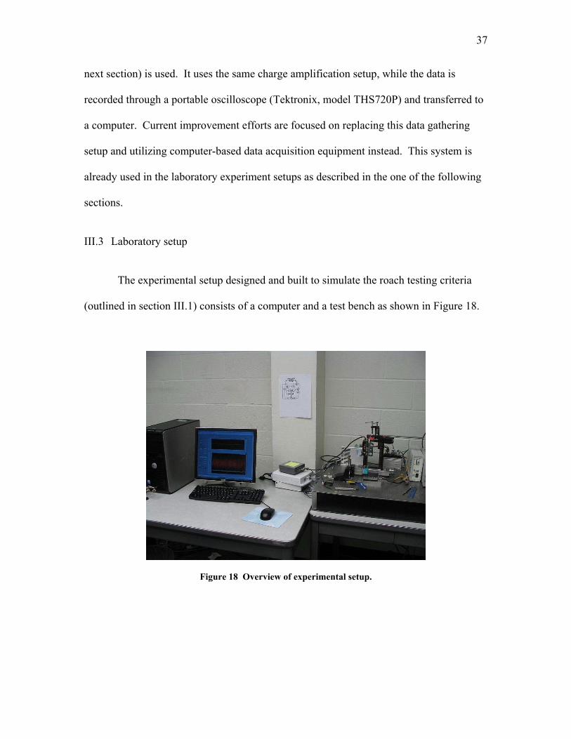
III.3 Laboratory setup
The experimental setup designed and built to simulate the roach testing criteria
(outlined in section III.1) consists of a computer and a test bench as shown in Figure 18.
Figure 18 Overview of experimental setup.

38
The setup allows for carrying out controlled sensor deformations and gathering
data feedback on sensor deflections and output signal. The results can be then analyzed
to understand the behavior and performance of sensors when mounted on roaches.
III.3.1 Mechanical setup
The mechanical components of the testing setup are mounted on a dampened
metal breadboard (Newport, model RG-52-4). They are shown in Figure 19.
Figure 19 Sensor mounting setup with the linear stage shown on the right.
A three-axis manual linear stage (Newport, model 460P-XYZ) shown on the left
provides fixed sensor support on one end. Its adjustability in all directions allows for
precise alignment of the sensor before it is tested. A single-axis miniature linear motor
stage (Parker Automation, model MX80L-T02-HS-D11-H3-L2) placed on the right is
responsible for generating the motion. The stage has a travel distance of 50mm with a
5µm resolution. Both elements are fitted with custom mounting blocks used for holding
the tested sensor in place as shown in Figure 20.
Fixed holder
Tested sensor
Linear stage
39
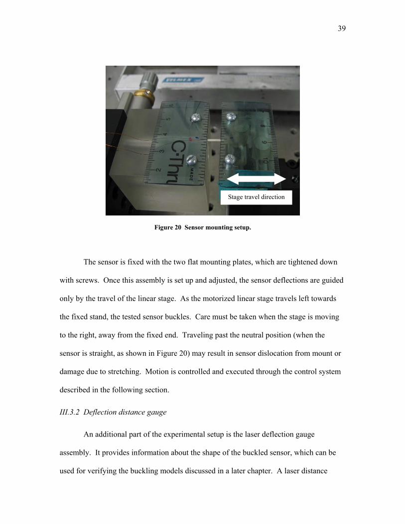
Figure 20 Sensor mounting setup.
The sensor is fixed with the two flat mounting plates, which are tightened down
with screws. Once this assembly is set up and adjusted, the sensor deflections are guided
only by the travel of the linear stage. As the motorized linear stage travels left towards
the fixed stand, the tested sensor buckles. Care must be taken when the stage is moving
to the right, away from the fixed end. Traveling past the neutral position (when the
sensor is straight, as shown in Figure 20) may result in sensor dislocation from mount or
damage due to stretching. Motion is controlled and executed through the control system
described in the following section.
III.3.2 Deflection distance gauge
An additional part of the experimental setup is the laser deflection gauge
assembly. It provides information about the shape of the buckled sensor, which can be
used for verifying the buckling models discussed in a later chapter. A laser distance
Stage travel direction
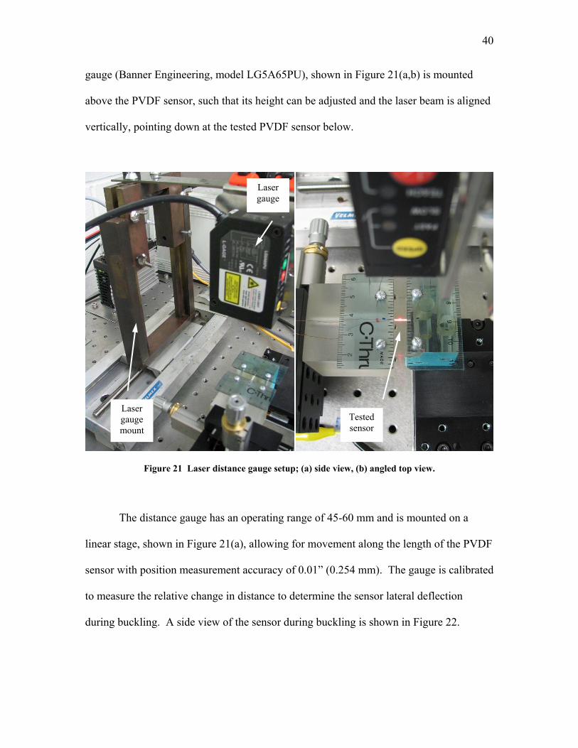
40
gauge (Banner Engineering, model LG5A65PU), shown in Figure 21(a,b) is mounted
above the PVDF sensor, such that its height can be adjusted and the laser beam is aligned
vertically, pointing down at the tested PVDF sensor below.
Figure 21 Laser distance gauge setup; (a) side view, (b) angled top view.
The distance gauge has an operating range of 45-60 mm and is mounted on a
linear stage, shown in Figure 21(a), allowing for movement along the length of the PVDF
sensor with position measurement accuracy of 0.01” (0.254 mm). The gauge is calibrated
to measure the relative change in distance to determine the sensor lateral deflection
during buckling. A side view of the sensor during buckling is shown in Figure 22.
Laser gauge mount
Laser gauge
Tested sensor
41
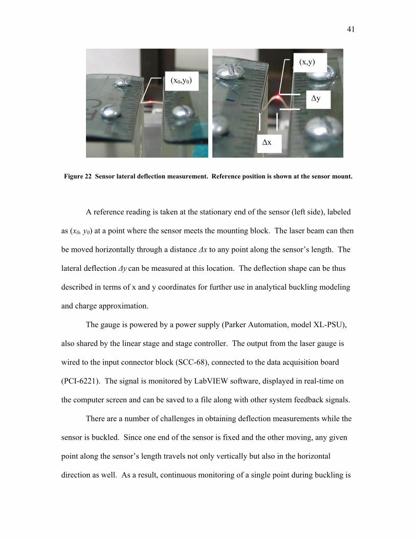
Figure 22 Sensor lateral deflection measurement. Reference position is shown at the sensor mount.
A reference reading is taken at the stationary end of the sensor (left side), labeled
as (x0, y0) at a point where the sensor meets the mounting block. The laser beam can then
be moved horizontally through a distance Δx to any point along the sensor’s length. The
lateral deflection Δy can be measured at this location. The deflection shape can be thus
described in terms of x and y coordinates for further use in analytical buckling modeling
and charge approximation.
The gauge is powered by a power supply (Parker Automation, model XL-PSU),
also shared by the linear stage and stage controller. The output from the laser gauge is
wired to the input connector block (SCC-68), connected to the data acquisition board
(PCI-6221). The signal is monitored by LabVIEW software, displayed in real-time on
the computer screen and can be saved to a file along with other system feedback signals.
There are a number of challenges in obtaining deflection measurements while the
sensor is buckled. Since one end of the sensor is fixed and the other moving, any given
point along the sensor’s length travels not only vertically but also in the horizontal
direction as well. As a result, continuous monitoring of a single point during buckling is
(x0,y0)
(x,y)
Δy
Δx

42
very difficult. Additionally, as the sensor deflects, its surface becomes curved and the
laser beam no longer strikes it at a perpendicular angle. For large sensor deflections the
angle between the beam and the film surface becomes increasingly small, and it may not
be possible to obtain an accurate deflection reading at every point along the sensor’s
length.
Given these challenges, it was decided to only use the deflection gauge in static
conditions, with the sensor already buckled. By traversing the laser gauge horizontally
and monitoring its position along the sensor’s length, sensor deflection can be found at
various points.
III.4 System control and data acquisition setup
In addition to controlling the linear stage movements, the control system is
responsible for gathering data such as position feedback, sensor output signal and lateral
deflection distance. The complete layout of the system is shown in Figure 23.

43
Figure 23 Laboratory system diagram.
System is operated by a desktop computer and controlled through a custom
written programming routine in LabVIEW software (National Instruments, LabVIEW
8.0). This software setup allows for executing predefined motion paths, live system
feedback monitoring, and recording data to file. The interface between the computer and
the experimental setup is handled by two control boards. The motion control board
(National Instruments, model PCI-7350) handles all movement commands and feedback,
while the data acquisition board (National Instruments, model PCI-6221) is responsible
for gathering data. Since the boards are mounted inside the computer, each one comes
with an external wiring terminal, where the physical wire connections with other
equipment are made. Signal inputs are connected to the input connector block (National
instruments, model SCC-68), while the motion control connections are made through the
motor interface block (National instruments, model UMI-7764). Specific aspects of
system operations and roles of other setup elements are outlined in the next section.
Computer
Laser (lateral deflection) signal
Lateral Deflection
Gauge
Linear stage position feedback
Sensor output signalInput
Connector Block
Motor Interface
Block
ViX Servo/Drive Controller
Power Supply
Charge Amplifier
Signal Conditioner
Linear Stage w/
Sensor Mount PVDF Sensor
NI Motion Control Board
NI Data Acquisition
Board
44
III.4.1 Motion control
Motion path of the motor linear stage (MX80L-T02-HS-D11-H3-L2) is defined
using Microsoft Excel, and converted through the Motion Assistant software (National
Instruments, Motion Assistant 2.0). It is then read through the custom control routine in
LabVIEW and executed by the motion control board (PCI-7350). The control signal is
sent through the universal motor interface (UMI-7764) to the linear stage controller
(Parker Automation, model ViX 250AH-DRIVE). The linear stage and the controller
responsible for its direct control are both powered with a DC power supply (XL-PSU).
III.4.2 Position feedback
The linear stage feedback signal is transferred back to the motion control board
and used by LabVIEW for real-time motion control during its operation. Feedback signal
is also wired into the data acquisition board (PCI-6221) via the input connector block
(SCC-68). It is then displayed on the computer screen and can be saved along with other
data inputs.
III.4.3 Sensor signal output
Piezoelectric sensors typically require special signal conditioning. Their output
impedance is normally higher than the input impedance of most measuring devices
(around several megaohms), resulting in negatively affected readings. The primary
purpose of signal conditioning is to reduce the impedance of the sensor output. Several
ways of achieving this goal have been studied,80,81 including applications of voltage
followers and current amplifiers.21 Presently, charge amplifiers are most common for

45
measuring charge generated by the piezoelectric sensor. An example of such a device is
shown in Figure 24.
Figure 24 Charge amplifier circuit.
The piezoelectric sensor can be modeled as a charge generator in parallel with the
sensor capacitance CP and capacitance of connecting cables CC. The charge generated is
transferred onto the feedback loop, where feedback capacitance CF and resistance RF can
be tuned for optimal system dynamic range. By increasing the feedback capacitance, the
circuit time constant is increased and the charge drain through the measurement system
can be reduced, allowing for measurements at near static conditions. However, with an
increased time constant the sensitivity is reduced and therefore pure static behavior
cannot be measured. Another benefit of the charge amplifier is that that effect of the lead
wire capacitance Cc is eliminated, therefore removing a possible source of measurement
error.38,82
CP CC
Op Amp
RF
CF
q
i -
+
V0
Piezoelectric sensor
46
In this research, the PVDF sensor leads are connected to an in-line charge
amplifier (PCB Piezotronics, model 422E03), where the charge output is converted to a
low-impedance voltage signal (the charge conversion is 1mV/1pC). The signal then goes
through an ICP® signal conditioner (PCB Piezotronics, model 482A21) where it is
further refined and transferred to the data acquisition board (PCI-6221) via the input
connector block (SCC-68). It is monitored by LabVIEW software, displayed in real-time
on the computer screen and can be saved to file along with other system data.
III.4.4 Data transfer and analysis
As mentioned earlier, during system operation, LabVIEW software monitors and
displays the system feedback information in real time. System user can save the data to
file at any time. It is stored in tab-delimited format, which can be opened with most
software packages. For the experiments presented here, Microsoft Excel was used for
data graphing and preliminary analysis.
III.5 Atomic force microscopy studies
In order to further the understanding of piezoelectric behavior in the sensor,
surface characterization analysis was carried out with the use of Atomic Force
Microscopy (AFM). The studies were focused on determining the relationship between
microstructures of PVDF and its piezoelectric behavior.
Atomic force microscopy is a technique which allows for detailed measurement
of the material surface topography with a resolution as low as a few nanometers. A
diagram of AFM operation is shown in Figure 25.
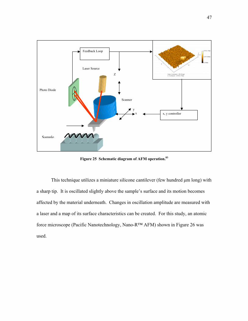
47
Figure 25 Schematic diagram of AFM operation.83
This technique utilizes a miniature silicone cantilever (few hundred μm long) with
a sharp tip. It is oscillated slightly above the sample’s surface and its motion becomes
affected by the material underneath. Changes in oscillation amplitude are measured with
a laser and a map of its surface characteristics can be created. For this study, an atomic
force microscope (Pacific Nanotechnology, Nano-R™ AFM) shown in Figure 26 was
used.
Feedback Loop
x, y controller
Z
Scanner
Laser Source
Photo Diode
Sample
y x
48
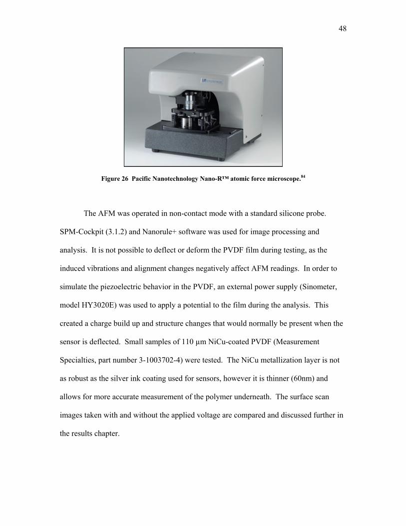
Figure 26 Pacific Nanotechnology Nano-R™ atomic force microscope.84
The AFM was operated in non-contact mode with a standard silicone probe.
SPM-Cockpit (3.1.2) and Nanorule+ software was used for image processing and
analysis. It is not possible to deflect or deform the PVDF film during testing, as the
induced vibrations and alignment changes negatively affect AFM readings. In order to
simulate the piezoelectric behavior in the PVDF, an external power supply (Sinometer,
model HY3020E) was used to apply a potential to the film during the analysis. This
created a charge build up and structure changes that would normally be present when the
sensor is deflected. Small samples of 110 µm NiCu-coated PVDF (Measurement
Specialties, part number 3-1003702-4) were tested. The NiCu metallization layer is not
as robust as the silver ink coating used for sensors, however it is thinner (60nm) and
allows for more accurate measurement of the polymer underneath. The surface scan
images taken with and without the applied voltage are compared and discussed further in
the results chapter.
49
CHAPTER IV
RESULTS AND ANALYSIS
This section discusses the experimental data, its interpretation and comparisons
with predicted results.
IV.1 Laboratory measurements
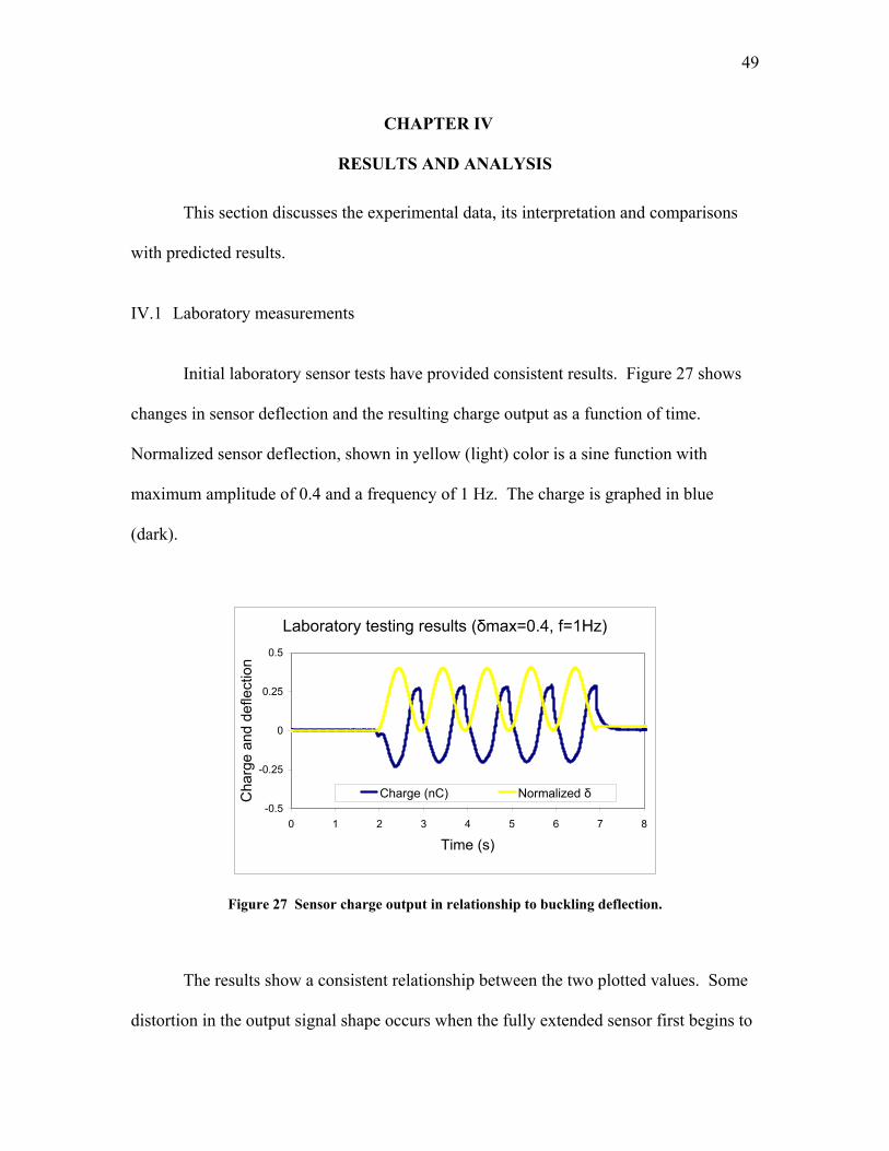
Initial laboratory sensor tests have provided consistent results. Figure 27 shows
changes in sensor deflection and the resulting charge output as a function of time.
Normalized sensor deflection, shown in yellow (light) color is a sine function with
maximum amplitude of 0.4 and a frequency of 1 Hz. The charge is graphed in blue
(dark).
Laboratory testing results (δmax=0.4, f=1Hz)
-0.5
-0.25
0
0.25
0.5
0 1 2 3 4 5 6 7 8
Time (s)
Cha
rge
and
defle
ctio
n
Charge (nC) Normalized δ
Figure 27 Sensor charge output in relationship to buckling deflection.
The results show a consistent relationship between the two plotted values. Some
distortion in the output signal shape occurs when the fully extended sensor first begins to
50
buckle (when δ=0). It is possible that these variations are introduced by the mechanical
control of the experiment system. Additionally, the charge output peaks seem to be
leading those of the deflection function. This will be discussed further along with the
approximation results in a later section.
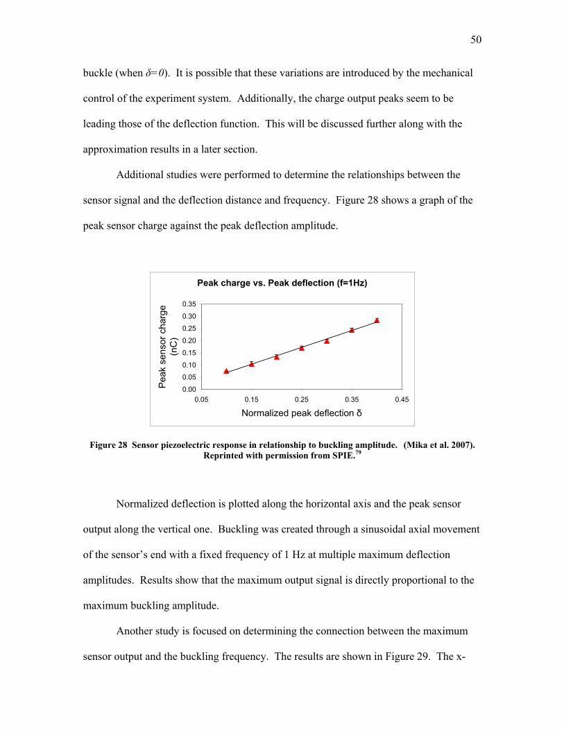
Additional studies were performed to determine the relationships between the
sensor signal and the deflection distance and frequency. Figure 28 shows a graph of the
peak sensor charge against the peak deflection amplitude.
Peak charge vs. Peak deflection (f=1Hz)
0.00
0.05
0.10
0.15
0.20
0.25
0.30
0.35
0.05 0.15 0.25 0.35 0.45
Normalized peak deflection δ
Pea
k se
nsor
cha
rge
(nC
)
Figure 28 Sensor piezoelectric response in relationship to buckling amplitude. (Mika et al. 2007). Reprinted with permission from SPIE.79
Normalized deflection is plotted along the horizontal axis and the peak sensor
output along the vertical one. Buckling was created through a sinusoidal axial movement
of the sensor’s end with a fixed frequency of 1 Hz at multiple maximum deflection
amplitudes. Results show that the maximum output signal is directly proportional to the
maximum buckling amplitude.
Another study is focused on determining the connection between the maximum
sensor output and the buckling frequency. The results are shown in Figure 29. The x-

51
axis is the frequency of axial deflection peaks, and the y-axis is the amplitude of the peak
sensor charge. The buckling was implemented by a sinusoidal deflection function with a
fixed deflection amplitude (δ=0.4) and at various frequencies.
Peak charge vs. Deflection frequency (δ=0.2)
0.00
0.05
0.10
0.15
0.20
0.25
0 2 4 6 8 10
Buckling frequency (Hz)
Pea
k se
nsor
cha
rge
(nC
)
Figure 29 Sensor piezoelectric response in relationship to buckling frequency. (Mika et al. 2007). Reprinted with permission from SPIE.79
No visible effect of the buckling frequency on the maximum output signal is
observed for the frequency range tested (1-10 Hz).
The study of sensor charge relationship to deflection amplitude and frequency
provides useful information about its application. Results show that charge output is
directly connected to the deflection amplitude, while no relationship with the frequency is
found. This suggests that individual charge signal peaks could be used to monitor the
number and size of insect steps.

52
IV.2 Roach experiments
Preliminary roach data was obtained by mounting a sensor across the coxa-femur
joint and allowing the insect to walk along the styrofoam ball as described earlier in
equipment setup section (II.4). The sensor did not seem to hinder the insects’ movements
and the charge generated seems fairly consistent as presented in Figure 30.
Roach testing results (coxa-femur joint)
-1.5
-1
-0.5
0
0.5
1
1.5
0 1 2 3 4 5 6
Time (s)
Sen
sor c
harg
e (n
C)
Figure 30 Sensor charge generated due to roach movement.
The multiple charge spikes shown in the graph can be correlated with individual
steps taken by the roach while walking. The shape of the output is different than the
results generated by the sinusoidal deflection in the lab. For future experiments new
deflection patterns can be developed (i.e. “saw-tooth” shape) to match the output results
seen here. Further roach studies can be carried out to develop the recognition of insect
movements and understanding of their behavior.
Larger scale experiments were initiated for this purpose. The sensor was attached
to the femur-tibia joint and multiple tests were performed. Along with charge data
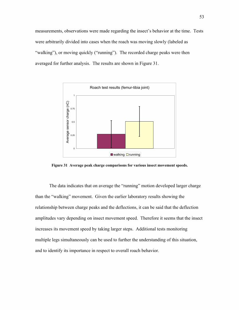
53
measurements, observations were made regarding the insect’s behavior at the time. Tests
were arbitrarily divided into cases when the roach was moving slowly (labeled as
“walking”), or moving quickly (“running”). The recorded charge peaks were then
averaged for further analysis. The results are shown in Figure 31.
Roach test results (femur-tibia joint)
0
0.25
0.5
0.75
1
Ave
rage
sen
sor c
harg
e (n
C)
walking running
Figure 31 Average peak charge comparisons for various insect movement speeds.
The data indicates that on average the “running” motion developed larger charge
than the “walking” movement. Given the earlier laboratory results showing the
relationship between charge peaks and the deflections, it can be said that the deflection
amplitudes vary depending on insect movement speed. Therefore it seems that the insect
increases its movement speed by taking larger steps. Additional tests monitoring
multiple legs simultaneously can be used to further the understanding of this situation,
and to identify its importance in respect to overall roach behavior.
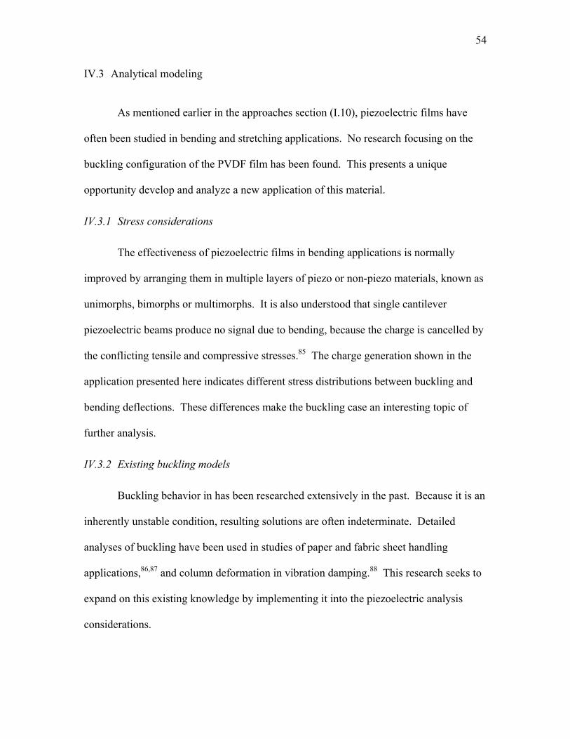
54
IV.3 Analytical modeling
As mentioned earlier in the approaches section (I.10), piezoelectric films have
often been studied in bending and stretching applications. No research focusing on the
buckling configuration of the PVDF film has been found. This presents a unique
opportunity develop and analyze a new application of this material.
IV.3.1 Stress considerations
The effectiveness of piezoelectric films in bending applications is normally
improved by arranging them in multiple layers of piezo or non-piezo materials, known as
unimorphs, bimorphs or multimorphs. It is also understood that single cantilever
piezoelectric beams produce no signal due to bending, because the charge is cancelled by
the conflicting tensile and compressive stresses.85 The charge generation shown in the
application presented here indicates different stress distributions between buckling and
bending deflections. These differences make the buckling case an interesting topic of
further analysis.
IV.3.2 Existing buckling models
Buckling behavior in has been researched extensively in the past. Because it is an
inherently unstable condition, resulting solutions are often indeterminate. Detailed
analyses of buckling have been used in studies of paper and fabric sheet handling
applications,86,87 and column deformation in vibration damping.88 This research seeks to
expand on this existing knowledge by implementing it into the piezoelectric analysis
considerations.

55
IV.3.3 Analytical models
A detailed analysis of PVDF sheet buckling has been performed for the purpose
of this research and is presented in the appendix section A.1.1. A solution relating the
charge output to the axial deflection δ in buckling can be obtained through numerical
approximation as:89,90
( )231 11
12 1 12e
IQ d cLh
π δ δ⎛ ⎞≈ + −⎜ ⎟⎝ ⎠
(4.1)
where the equilibrium (quasi-static) condition charge is labeled as eQ , the
piezoelectric constant is 31d and the elastic constant is 11c . Other terms include
normalized axial displacement of the sensor end δ , sensor half-length L , thickness h
and cross-sectional moment of inertia I . Figure 32 shows a graph of charge output and
axial deflection as a function of time.
Figure 32 Graphs of normalized sensor charge and sensor-end axial displacement δ during buckling.90
56
As described in equation 4.1, and confirmed by Figure 32, the charge build up
during buckling is dependent on the deflection, which is the input variable. In this case,
the axial deflection of sensor’s end δ varies over time as a cosine function. Further
comparisons between the estimated and experimental charge are discussed in the
following chapter.
IV.3.4 Lateral deflection analysis
No detailed lateral deflection experiments have been performed so far. Their
purpose is to verify the sensor deflection shape assumed for the charge modeling
derivations. As explained in detail in appendix section A.1.1, the sensor shape during
buckling can be defined by a sinusoidal function. It expected that this will be confirmed
by laser beam lateral deflection experiments carried out in the future phases of this
project.
IV.3.5 Model comparisons
The approximate solutions obtained with the use of the sensor deflection model
can be compared to the laboratory results for verification. At this time, there exist
numerical discrepancies between the two sets, making a quantitative comparison between
them questionable. It is still possible to use the analytical calculations for evaluating
shape similarities between experimental and approximate charge graphs. Laboratory
results, already presented earlier, are shown in Figure 33.

57
Laboratory testing results (δmax=0.4, f=1Hz)
-0.5
-0.25
0
0.25
0.5
0 1 2 3 4 5 6 7 8
Time (s)
Cha
rge
and
defle
ctio
n
Charge (nC) Normalized δ
Figure 33 Sensor output in relationship to buckling deflection – laboratory results.
The approximate analytical results scaled for the purpose of comparison are
presented in Figure 34.
Approximate results (δmax=0.4, f=1Hz)
-0.5
-0.25
0
0.25
0.5
0 1 2 3 4 5 6 7 8
Time (s)
Cha
rge
and
defle
ctio
n
Charge Qe(nC) Normalized δ
Figure 34 Sensor output in relationship to buckling deflection – scaled analytical results.
As shown in these graphs, mathematical and experimental results provide similar
sensor charge patterns during buckling. In both cases the charge becomes negative as the
PVDF film is being deformed. The difference between them is that in laboratory tests,
58
the charge increases reaching a positive peak as the sensor returns to normal. This is not
the case for the analytical results, possibly due to dynamic charge dissipation, which is
not accounted for in the mathematical model. Additional discrepancies include slight
output signal distortion visible in the experimental data, likely caused by the mechanical
control of the linear stage, as discussed earlier. Most importantly, the laboratory charge
plot seems to lead the deflection curve, which is not the case for analytical data graph.
The causes of this are unknown at this time.
IV.4 Microscopic analysis results
Microstructure studies were performed using the AFM setup described in the
experimental setup section (III.5). Results were analyzed to gain the understanding of the
piezoelectric effect on the material microstructures. Figure 35 shows the AFM height
(topography) image and phase (material properties) image scans taken at various testing
conditions.
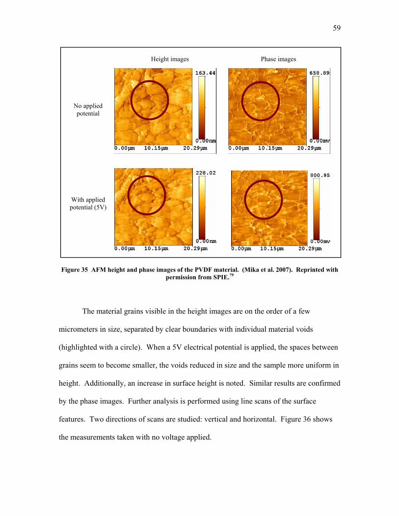
59
Figure 35 AFM height and phase images of the PVDF material. (Mika et al. 2007). Reprinted with permission from SPIE.79
The material grains visible in the height images are on the order of a few
micrometers in size, separated by clear boundaries with individual material voids
(highlighted with a circle). When a 5V electrical potential is applied, the spaces between
grains seem to become smaller, the voids reduced in size and the sample more uniform in
height. Additionally, an increase in surface height is noted. Similar results are confirmed
by the phase images. Further analysis is performed using line scans of the surface
features. Two directions of scans are studied: vertical and horizontal. Figure 36 shows
the measurements taken with no voltage applied.
Height images
With applied potential (5V)
No applied potential
Phase images

60
Figure 36 AFM Line scans with no applied potential: (a) horizontal, (b) vertical.
Figure 37 shows the readings taken over the same area with an applied potential
of 5V.
a
b
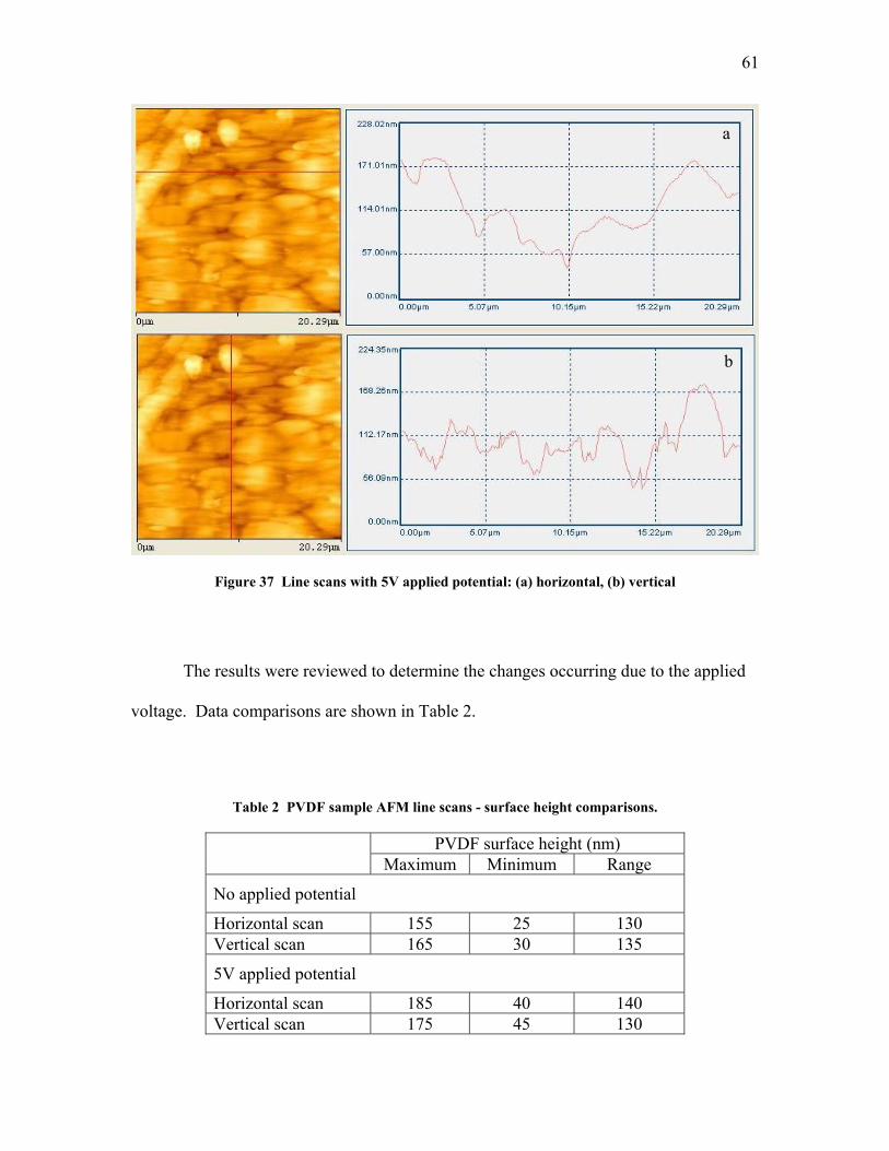
61
Figure 37 Line scans with 5V applied potential: (a) horizontal, (b) vertical
The results were reviewed to determine the changes occurring due to the applied
voltage. Data comparisons are shown in Table 2.
Table 2 PVDF sample AFM line scans - surface height comparisons.
PVDF surface height (nm) Maximum Minimum Range
No applied potential
Horizontal scan 155 25 130 Vertical scan 165 30 135
5V applied potential
Horizontal scan 185 40 140 Vertical scan 175 45 130
a
b

62
The results do not confirm the suspected changes in material grains. It is possible
that these perceived changes of surface structures are due the differences in height scales
of the images in Figure 35. Instead, the line scans show an overall increase of surface
height with applied voltage. This is likely an example of an inverse of the piezoelectric
effect discussed earlier (section I.6), where as shown in Equation 1.16, the charge build
up in the film is related to the change of its thickness.
This behavior is likely due to the dipole changes inside the piezomaterial. Under
an applied potential, the dipole alignment affects the material properties, leading to
changes in thickness. Detailed mechanisms of surface microstructure changes within
PVDF are an interesting research topic and have been studied in the past.79,91,92
Performing in-situ microscopy studies on the piezoelectric effects remains a new and
exciting area of research and future developments can be expected.

63
CHAPTER V
CONCLUSIONS
This project has been an important step in developing a new research area. It has
achieved three main goals:
- developed a methodology and hardware for sensor testing,
- completed initial sensor testing and analysis,
- proved feasibility of insect studies with piezoelectric sensors.
Specifically, two test systems have been designed and built. One for analyzing
the piezoelectric response in PVDF films due to buckling, and another for sensor
application studies on the roach, Blaberus discoidalis. An understanding of piezoelectric
materials has been achieved through study of existing literature and analysis of new
laboratory experiments. A new sensor application was shown to be a promising tool for
future studies of insects, their movements and behaviors. Also, initial steps were taken in
the area of surface microstructure studies of PVDF and their relationship with the
piezoelectric effect.
A knowledge base of materials, sensors, equipment setups and basic insect
behavior has been established and documented for use in the next phases of the project.
Given the early stage of this research, a number of future improvements can be made.
The following topics have been identified as possible areas of future developments:
- improved sensor manufacturing processes (die cutting techniques, conductive
adhesives, protective coatings - i.e. parylene),
- new sensor-to-roach attachment methods (glues or clamps),

64
- extensive roach testing (multiple-leg testing in combination with behavioral
monitoring to facilitate the identification and understanding of insect
movement patterns and their connection with piezo sensor response).
The application of the above suggestions will likely further increase the reliability
and usefulness of thin film PVDF sensors as tools for physiological studies of insects.

65
REFERENCES
1 J. Curie and P. Curie, C. R. Acad Sci. Paris 91, 294, (1880); 91, 383 (1880).
2 L. Kelvin, Baltimore Lectures (C.J. Clay & Sons, London, 1904).
3 P. Langevin, French Patent No. 505 (17 September 1918), p. 703.
4 W. G. Cady, Piezoelectricity (McGraw Hill, New York, 1946; Dover, New York, 1964).
5 H. Kawai, Japan J. Appl. Phys. 8, 975 (1969).
6 M. G. Broadhurst, G. T. Davis, in Electrets edited by G. M. Sessler (Springer-Verlag, Berlin, vol. 33, 1980), pp. 285-319.
7 M. G. Broadhurst, G. T. Davis , J. E. McKinney, and R. E. Collins, J. Appl. Phys. 49,
4992 (1978). 8 G. M. Sessler, J. Acoust. Soc. Am. 70, 1596 (1981).
9 R. Hasegawa, Y. Takahashi, Y. Chatani, and H. Tadokoro, Polym. J. 3, 600 (1972).
10 M. A. Bachmann and J. B. Lando, Macromolecules 14, 40 (1981).
11 S. Weinhold, M. H. Litt, and J. B. Lando, Macromolecules 13, 1178 (1980).
12 A. J. Lovinger, Macromolecules 14, 322 (1981).
13 A. J. Lovinger, Macromolecules 15, 40 (1982).
14 G. T. Davis, J. E. McKinney, M. G. Broadhurst, and S. C. Roth, J. Appl. Phys. 49, 4998 (1978).
15 A. J. Lovinger, Science 220, 1115 (1983).
16 H. D. Keith and F. J. Padden, Jr., J. Appl. Phys. 35, 1270 (1964).
17 A. J. Lovinger, Polymer 21, 1317 (1980).
18 A. J. Lovinger, J. Appl. Phys. 52, 5934 (1981).
19 K. Nakagawa and Y. Ishida, J. Polym. Sci. Phys. Ed. 11, 2153 (1973).
20 B. L. Farmer, A. J. Hopfinger, and J. B. Lando, J. Appl. Phys. 43, 4293 (1972).
66
21 C. K. Lee and T. C. O'Sullivan, J. Acoust. Soc. Am. 90, 949 (1991).
22 R. M. Bozorth, Ferromagnetism (Van Nostrand, New York, 1951; IEEE Press, Piscataway, 1993).
23 J. S. Harrison and Z. Ounaies, NASA/CR-2001-211422, ICASE Report No. 2001-43
(2001). 24 H. Sussner and K. Dransfeld, J. Polym. Sci. Polym. Phys. Ed. 16, 529 (1978).
25 R. G. Kepler and R. A. Anderson, J. Appl. Phys. 49, 1232 (1978).
26 J. P. Luongo, J. Polym. Sci. A-2 10, 1119 (1 972).
27 K. Tashiro, M. Kobayashi, H. Tadakoro, and E. Fukada, Macromolecules 13, 691 (1980).
28 T. Furukawa, IEEE Trans. Electr. Insul. 24, 375 (1989).
29 G. M. Sessler, D. K. Das-Gupta, A. S. DeReggi, W. Eisenmenger, T. Furukawa, J. A. Giacometti, and R. Gerhard-Multhaupt, IEEE Trans. Electr. Insul. 27, 872 (1992).
30 E. P. Adams, J. Franklin Inst. 204, 469 (1927).
31 F. I. Mopsik and M. G. Broadhurst, J. Appl. Phys. 46, 4204 (1975).
32 H. Ohigashi, J. App. Phys. 47, 949 (1976).
33 R. Hayakawa and Y. Wada, Rep. Progr. Polym. Phys. Jpn. 19, 321 (1976).
34 Y. Wada and R. Hayakawa, Ferroelectrics 32, 115 (1981).
35 A. Ballato, IEEE Trans. Ultrason., Ferroelect., Freq. Control 42, 916 (1995).
36 W. P. Mason, Physical Acoustics and the Properties of Solids (Van Nostrand, Princeton, 1958).
37 A. H. Meitzler, H. F. Tiersten, A. W. Warner, D. Berlincourt, G. A. Coquin, and F. S.
Welsh III, IEEE Standard on Piezoelectricity (IEEE, New York , 1988).
38 J. Sirohi, I. Chopra, J. Intellig. Mat. Sys. Struct. 11, 246 (2000).
39 E. Fukada and T. Furukawa, Ultrasonics 1, 31 (1981).
40 T. Yamada, J. Appl. Phys. 53, 6335 (1982).
67
41 V. V. Kochervinskii, Russ. Chem. Rev. 65, 865 (1996).
42 T. Furukawa and T. T. Wang, in The Applications of Ferroelectric Polymers edited by T. T. Wang, J. M. Herbert, and A. M. Glass (Blackie, U.K., 1987), pp. 66-117.
43 K. Tashiro, H. Tadakoro, and M. Kobayashi, Ferroelectrics 32, 167 (1981).
44 H. J. Shaw, D. Weinstein, L. T. Zitelli, C. W. Frank, R. C. DeMattei, and K. Fesler, Proc. 1980 Ultrason. Symp. (IEEE, Piscataway, 1980), pp. 927-940.
45 E. L. Nix, L. Holt, J. C. McGrath, and I. M. Ward, Ferroelectrics 32, 103 (1981).
46 E. Fukada and T. Sakurai, Polym. J. 2, 656 (1971).
47 G. Gerliczy and R. Betz, Sensors and Actuators 12, 207 (1987).
48 J. McKinney, G. T. Davis, and M. G. Broadhurst, J. Appl. Phys. 51, 1676 (1980).
49 P. D. Southgate, Appl. Phys. Lett. 28, 250 (1976).
50 Arkema, Inc., http://www.arkema-inc.com/literature_techpoly.cfm?pag=102; http://www.arkema-inc.com/index.cfm?pag=102, Accessed May 2007.
51 G. Eberle, H. Schmidt, and W. Eisenmenger, IEEE Trans. Dielectrics Electr. Insul. 3, 624 (1996).
52 Y. Bar-Cohen, Electroactive Polymer (EAP) Actuators as Artificial Muscles: Reality,
Potential andChallenges (SPIE, Bellingham, 2001), p. 615. 53 D. De Rossi and P. Dario, Medical Applications of Piezoelectric Polymers edited by P.
M. Galletti, D. E. De Rossi, and A. S. De Reggi (Gordon and Breach, New York, 1988), p. 83.
54 Measurement Specialties, http://www.meas-spec.com/myMeas/download/pdf/english/ piezo/techman.pdf, Accessed May 2007.
55 D. Fox, Ferroelectrics 115, 215 (1991).
56 A. M. Vinogradov, S. C. Schumacher, and E. M. Rassi, J. Appl. Electromag. Mech. 22, 39 (2005).
57 Y. Gu, R. L. Clark, C. R. Fuller, and A. C. Zander, J. Vibration and Acoustics 116, 303
(1994). 58 H. S. Tzou, J. Robotic Systems 6, 745 (1989).
68
59 F. Delcomyn, J. Exp. Biol. 54, 443 (1971).
60 F. Delcomyn, J. Exp. Biol. 133, 111 (1977).
61 N. J. Cowan, J. Lee, and R. J. Full, J. Exp. Biol. 209, 1617 (2006).
62 J. T. Watson and R. E. Ritzmann, J. Comp. Physiol. 182, 11 (1998).
63 J. T. Watson and R. E. Ritzmann, J. Comp. Physiol. 182, 23 (1998).
64 J. T. Watson, R. E. Ritzmann, and A. J. Pollack, J. Comp. Physiol. 188, 55 (2002).
65 D. R. Reynolds and J. R. Riley, Comput. Electron. Agr. 35, 271 (2002).
66 W. Kutsch, Theory in Biosciences 118, 29 (1999).
67 I. G. Priede and S. M. Swift, Ecology 74, 1908 (1993).
68 T. G. Wolcott, J. Exp. Mar. Biol. Ecol. 193, 257 (1995).
69 F. G. Barth and P. Pickelmann, J. Comp. Physiol. 103, 39 (1975).
70 A. Skordos, P. H. Chan, J. F. V. Vincent, and G. Jeronimidis, Phil. Trans. R. Soc. Lond. A 360, 239 (2002).
71 University of Massachusetts, http://www.bio.umass.edu/biology/kunkel/ cockroach.html, Accessed May 2007.
72 B. E. Hagenbuch, P. G. Koehler, R. S. Patterson, and R. J. Brenner, J. Med. Entomol.
25, 377 (1988). 73 W. J. Bell and K. G. Adiyodi, The American Cockroach (Chapman and Hall, London,
1981). 74 M. K. Rust, D. A. Reierson, and K. H. Hansgen, J. Med. Entomol. 28, 210 (1991).
75 Measurement Specialties, http://www.meas-spec.com/myMeas/MEAS_download/ Catalogs/Piezo/catalog_price_list.pdf, Accessed May 2007.
76 Y. Fu, E. C. Harvey, M. K. Ghantasala, and G. M. Spinks, Smart Mater. Struct. 15, S141-S146 (2006).
77 Courtesy of H. Lee, Dept. of Mat. Sci. Engr., Texas A&M University.
78 R. J. Full and M. S. Tu, J. Exp. Biol. 148, 129 (1990).

69
79 B. Mika, H. Lee, J. M. Gonzalez, S. B. Vinson, and H. Liang, Proc. of SPIE 6528,
652817 (2007). 80 D. F. Stout and M. Kaufman, Handbook of Operational Amplifier Circuit Design
(McGraw Hill, New York , 1976).
81 J. W. Dally, W. F. Riley, and K. G. McConnell, Instrumentation for Engineering Measurement. (John Wiley & Sons, New York, 1993).
82 P. Horowtiz and W. Hill, The Art of Electronics (Cambridge U. P., Cambridge, England, 1980).
83 T. Jee, MS Thesis, Dept. of Mech. Engr., Texas A&M University, 2005.
84 Pacific Nanotechnology, http://www.pacificnanotech.com/nano-r-afm.html, Accessed May 2007. 85 Q. M. Wang, X. Du, B. Xu, and L. E. Cross, J. Appl. Phys. 85, 1702 (1999).
86 C. Y. Wang, ASME J. Appl. Mech. 51, 278 (1984).
87 S. T. Santillan, L. N. Virgin, and R. H. Plaut, ASME J. Appl. Mech. 73, 664 (2006).
88 H. S. Yoon, G. Washington, and A. Danak, J. Intellig. Mat. Sys. Struct., 16, 877 (2005).
89 K. S. Moon, H. Liang, J. Yi, and B. Mika, Proc. of SPIE 6529, 65290 (2007).
90 J. Yi, Dept of Mech. Engr., San Diego State University (unpublished manuscript), (2007).
91 T. Jee, H. Lee, B. Mika, and H. Liang, Tri. Lett. 26, 125 (2007).
92 S. Mani, R. Perez, H. Lee, Z. Ounaies, W. Hung, and H. Liang, J. Trib., in press (2007).

70
APPENDIX A
EQUATIONS AND DERIVATIONS
A.1 Approximate charge generation during buckling
Following is a derivation of the approximate charge resulting due to sensor
buckling deformation based on the work of Yi90 and other authors referenced within.*
A.1.1 Analytical derivation
We denote the PVDF elastica size as 2L (length), b (width), and h (height),
respectively. Since the PVDF film is very thin (around 110 µm), we can consider this
sensor as a thin strip and use the heavy elastica model discussed by Wang86 and Santillan
et al.87 to model the deflection of the post-buckling shape of the sensor. We consider a
PVDF based elastica that is under buckling formation as shown in Figure A1(a). One end
of the PVDF elastica is clamped at a fixed platform and the other end is also clamped
with a moving platform. The deformation of the moving end is denoted as Δ(t) and the
applied force is denoted as F(t).
* Reprinted with permission from: “On Symmetric Buckling of a Finite Flat-Lying Heavy Sheet” by C.Y. Wang, 1984. ASME Journal of Applied Mechanics, Vol. 51, p.278–282, Copyright ©1984 by ASME. and “Post-Buckling and Vibration of Heavy Beam on Horizontal or Inclined Rigid Foundation” by S. T. Santillan, L. N. Virgin, and R. H. Plaut, 2006. ASME Journal of Applied Mechanics, Vol. 73, p.664–671, Copyright ©2006 by ASME.

71
Figure A1 : (a) Schematic of the buckling shape of a PVDF sensor; (b) free body diagram of a differential element of the sensor.
We choose the XY coordinate with origin O at the fixed end of the PVDF sensor.
The deflection at point R(X,Y) of the PVDF strip is parameterized by the arc-length S
(with S=0 at point O) as shown in Figure A1 (a). The deflection angle θ(S) is defined as
the tangent directional angle with the X axis. Figure A1 (b) shows the free body diagram
of at point R. The internal forces along X and Y directions on the differential element dS
at time T are denoted as F(S,T) and Q(S,T), respectively. The bending moment at point R
is denoted as M(S,T) at time T. We can then obtain the motion equation for the elastica
as:†
2 2
2 2
cos , sin , ,
, , cos sin ,
X Y MS S S EIF X Q Y Mg Q FS T S T S
θθ θ κ
ρ ρ ρ θ θ
∂ ∂ ∂= = = =
∂ ∂ ∂∂ ∂ ∂ ∂ ∂
= − = − − = −∂ ∂ ∂ ∂ ∂
(A1.1)
where E is Young’s modulus of the PVDF film, I is the second moment of the
cross sectional area of the elastica with respect to the bending axis, and ρ is the mass
density per unit length of the PVDF material. Before we proceed to put Eq. (A1.1) into
† For notation simplicity, we drop the variable dependence on arc length S and time T.

72
dimensionless equations, we first determine the electric charge Qe. We consider the
linear constitutive relationships37 for piezoelectricity among strain (S), stress (T), electric
field (E), and electric displacement (D)
Ej ji i jm m
Em mj j km k
S s T d
D d T
ε
ε ε
= +
= + (A1.2)
where s is the compliance matrix, d is the piezoelectric matrix, and ε is the
permittivity matrix. Moreover, we assume that the electric field is approximately close to
zero due to the quasi-static estimation in this study. The accumulated electric charge Qe
due to the bending and axial forces on the two sides of the PVDF sensor electrodes can
be calculated as:88
3 31 11 1eA A
Q D dA d c S dA= =∫ ∫ (A1.3)
where D3 is electric displacement along 33 direction and dA is the electrode area
of the strip surface. Since the PVDF film is not stiff, we consider the electric charge is
mainly generated by the bending of the PVDF film. For the differential PVDF element
shown in Figure A1(b), the element is under both bending and axial force and the neutral
axis (NN’ in Figure A1(b)) of the PVDF film will no longer be the film centroidal axis
(CC’ in Figure A1(b)). Denote the distance between NN’ and CC’ as zN at location S and
time T. Then the axial force Fa along the sensor film is given by:
cos sinaF F Qθ θ= + (A1.4)
and the bending moment is M. Note that the strain S = 0 along NN’ and using the
superposition of axial force and bending moment effects, we can calculate zN as:
2 21 1 cos sin12 12
aN
F F Qz h hM M
θ θ+= = (A1.5)

73
Then the strain S1 of the single PVDF film can be calculated as:
21
1 cos sin cos sin12N
F Q M F QS z hM EI Ebhθ θ θ θκ + +
= = = (A1.6)
where we use I = 3112
bh for a rectangular cross section area. Due to the
symmetry of the film we only consider S >0 and thus write Eq. (A1.3) as:
( )31 1131 11
0 0
2 cos sinL L
e Nd cQ bd c z dS F Q dS
Ehκ θ θ= = +∫ ∫ (A1.7)
We can use the following non-dimensional quantities87 for dynamic equations of
motion given by Eq. (A1.1):
2
2 32
2
, , , , , ,
, , ,
X Y S ML FLx y s m fL L L L EI EIQL gL T EIq w t wLEI EI L EI
δ
ρ ρρ
Δ= = = = = =
= = = Ω = (A1.8)
and Eq. (A1.1) becomes:
2 2
2 2
cos , sin , ,
, , cos sin ,
x y ms s sf x q y mw q fs t s t s
θθ θ
θ θ
∂ ∂ ∂= = =
∂ ∂ ∂∂ ∂ ∂ ∂ ∂
= − = − − = −∂ ∂ ∂ ∂ ∂
(A1.9)
Furthermore, we can separate the variables as the sum of equilibrium and
dynamic components, namely:
( , ) ( ) ( )sin( ), ( , ) ( ) ( )sin( ),( , ) ( ) ( )sin( ), ( , ) ( ) ( )sin( ),( , ) ( ) ( )sin( ), ( , ) ( ) ( )sin( ),
e d e d
e d e d
e d e d
x s t x s x s t y s t y s y s ts t s s t m s t m s m s t
f s t f s f s t q s t q s q s tθ θ θ
= + Ω = + Ω= + Ω = + Ω= + Ω = + Ω
(A1.10)
Then we can write the equations that the equilibrium components must satisfy as:
cos , sin , , cos sin ,e e e ee e e e e e e
x y mm q fs s s s
θθ θ θ θ∂ ∂ ∂ ∂= = = = −
∂ ∂ ∂ ∂ (A1.11)

74
The normalized force qe satisfies:
( )eq s sw= (A1.12)
since qe is the normalized gravity force from S=0. The boundary conditions for
Eq. (A1.11) are:
(0) (0) (0) 0, (1) 1 , (1) 0e e e e ex y xθ δ θ= = = = − = (A1.13)
For the electric charge generated by the buckling, we only consider the charge
generated by the quasi-static equilibria and therefore we can write Eq. (A1.7) as:
( )1
31 110
2 cos sine e e e eIQ bd c f q ds
Lhθ θ= +∫ (A1.14)
A.1.2 Approximate solution
The exact analytical solutions for differential equations given by Eq. (A1.11) with
boundary conditions (A1.13) cannot be obtained.86 Therefore, we approximate the
boundary value problem following the same approach taken by Wang.86 For small
deflections θ<<1 for the PVDF film, we can assume that w<<1. We assume w = ε3<<1
and we can approximate θe(s), xe(s), ye(s) and fe(s) as:
3 5 2 40 1 0 1
3 5 2 40 1 0 1
( ) ( ) ( ) 0( ), ( ) ( ) ( ) 0( ),
( ) ( ) ( ) 0( ), ( ) ( ) ( ) 0( ),e e
e e
s s s x s x s x s
y s y s y s f s f s f s nonumber
θ εθ ε θ ε ε ε
ε ε ε ε ε
= + + = + +
= + + = + + (A1.15)
3 3 5 2 2 40 0 1 0
1 1sin ( 6 ) 0( ), cos 1 ( ) 0( ),6 2e eθ εθ ε θ θ ε θ ε θ ε= + − + + = + − + (A1.16)
Using the above approximation to Eq. (A1.11) and taking the first two terms in
each equation, we can obtain:
20 10
11,2
dx dxds ds
θ= = − (A1.17)
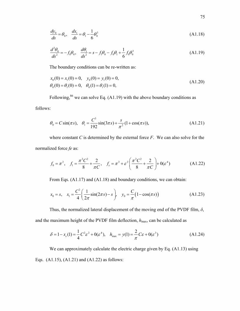
75
30 10 1 0
1,6
dy dxds ds
θ θ θ= = − (A1.18)
230 1
0 0 1 0 0 1 0 02 2
1,6
d df s f f fds dsθ θθ θ θ θ= − = − − + (A1.19)
The boundary conditions can be re-written as:
0 1 0 1
0 1 0 1
(0) (0) 0, (0) (0) 0,(0) (0) 0, (1) (1) 0,
x x y yθ θ θ θ
= = = == = = =
(A1.20)
Following,86 we can solve Eq. (A1.19) with the above boundary conditions as
follows:
3
0 1 2sin( ), sin(3 ) (1 cos( )),192C sC s s sθ π θ π π
π= = + + (A1.21)
where constant C is determined by the external force F. We can also solve for the
normalized force fe as:
2 2 2 22 2 2 4
0 12 2, , 0( )
8 8eC Cf f f
C Cπ ππ π ε ε
π π⎛ ⎞
= = + = + + +⎜ ⎟⎝ ⎠
(A1.22)
From Eqs. (A1.17) and (A1.18) and boundary conditions, we can obtain:
( )2
0 1 01, sin(2 ) , 1 cos( )
4 2C Cx s x s s y sπ π
π π⎛ ⎞= = − = −⎜ ⎟⎝ ⎠
(A1.23)
Thus, the normalized lateral displacement of the moving end of the PVDF film, δ,
and the maximum height of the PVDF film deflection, hmax, can be calculated as
2 2 4 3max
1 21 (1) 0( ), (1) 0( )4ex C h y Cδ ε ε ε ε
π= − = + = = + (A1.24)
We can approximately calculate the electric charge given by Eq. (A1.13) using
Eqs. (A1.15), (A1.21) and (A1.22) as follows:
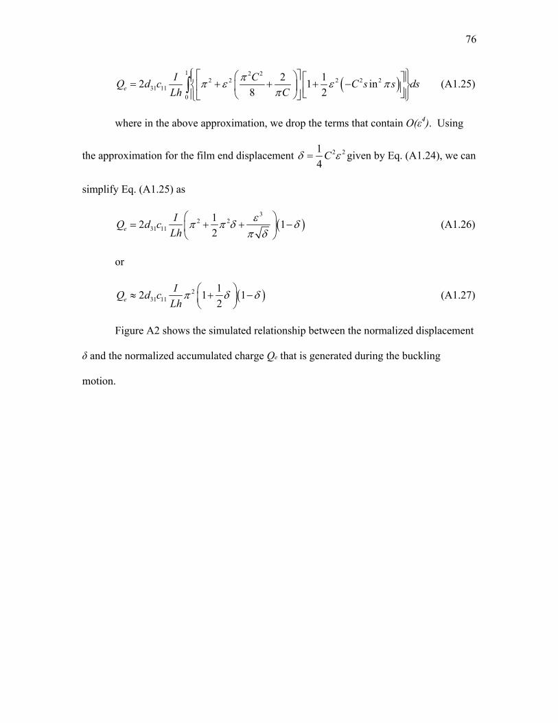
76
( )1 2 2
2 2 2 2 231 11
0
2 12 1 in8 2e
I CQ d c C s s dsLh C
ππ ε ε ππ
⎧ ⎫⎡ ⎤⎛ ⎞⎪ ⎪⎡ ⎤= + + + −⎨ ⎬⎢ ⎥⎜ ⎟ ⎢ ⎥⎣ ⎦⎝ ⎠⎪ ⎪⎣ ⎦⎩ ⎭∫ (A1.25)
where in the above approximation, we drop the terms that contain O(ε4). Using
the approximation for the film end displacement 2 214
Cδ ε= given by Eq. (A1.24), we can
simplify Eq. (A1.25) as
( )3
2 231 11
12 12e
IQ d cLh
επ π δ δπ δ
⎛ ⎞= + + −⎜ ⎟
⎝ ⎠ (A1.26)
or
( )231 11
12 1 12e
IQ d cLh
π δ δ⎛ ⎞≈ + −⎜ ⎟⎝ ⎠
(A1.27)
Figure A2 shows the simulated relationship between the normalized displacement
δ and the normalized accumulated charge Qe that is generated during the buckling
motion.

77
Figure A2 Simulated relationship between the normalized accumulated charge Qe and the normalized end displacement δ during a buckling motion.
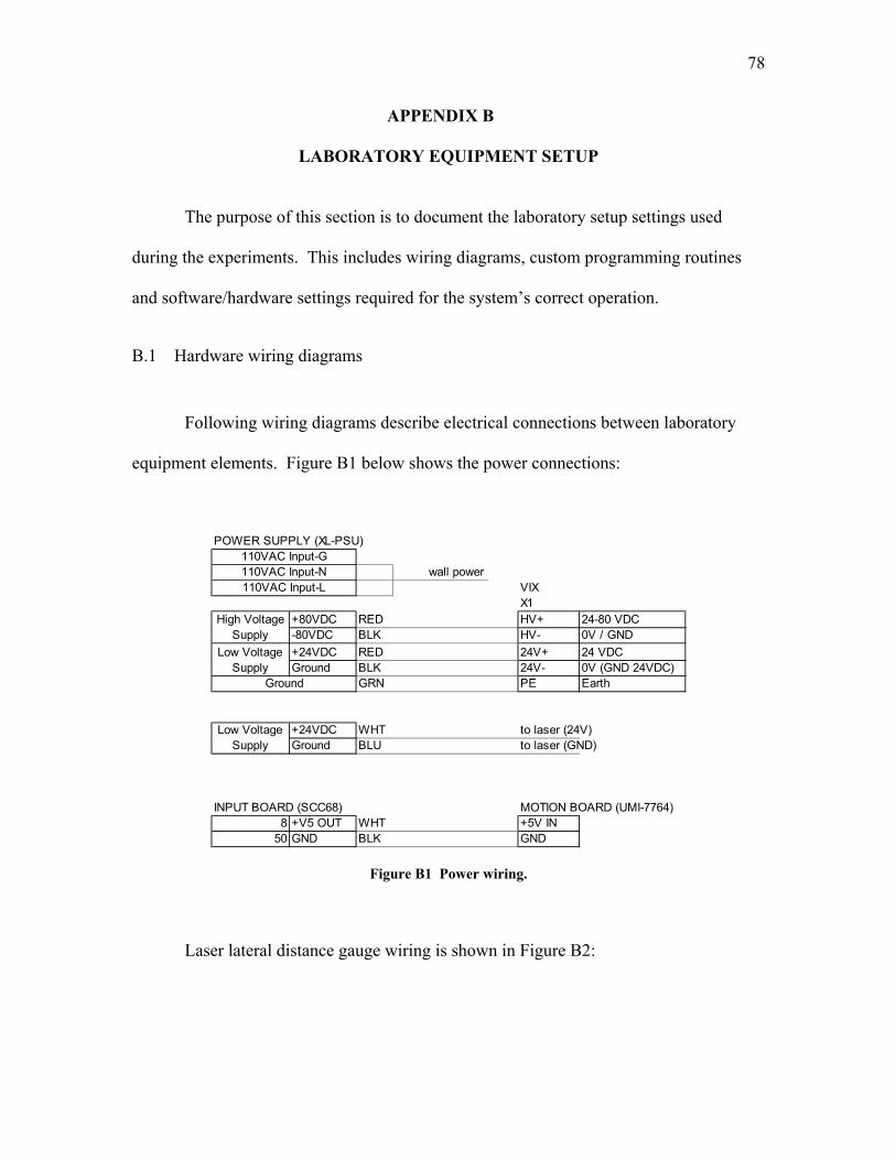
78
APPENDIX B
LABORATORY EQUIPMENT SETUP
The purpose of this section is to document the laboratory setup settings used
during the experiments. This includes wiring diagrams, custom programming routines
and software/hardware settings required for the system’s correct operation.
B.1 Hardware wiring diagrams
Following wiring diagrams describe electrical connections between laboratory
equipment elements. Figure B1 below shows the power connections:
POWER SUPPLY (XL-PSU)
wall powerVIXX1
+80VDC RED HV+ 24-80 VDC-80VDC BLK HV- 0V / GND+24VDC RED 24V+ 24 VDCGround BLK 24V- 0V (GND 24VDC)
GRN PE Earth
+24VDC WHT to laser (24V)Ground BLU to laser (GND)
INPUT BOARD (SCC68) MOTION BOARD (UMI-7764)8 +V5 OUT WHT +5V IN
50 GND BLK GND
High VoltageSupply
Low VoltageSupply
Low VoltageSupply
110VAC Input-G110VAC Input-N110VAC Input-L
Ground
Figure B1 Power wiring.
Laser lateral distance gauge wiring is shown in Figure B2:

79
LASER (LG5A65PU)BLU Ground BRN WHT to power supply (24V)BRN Power BLK cable GRNGRN On/OffWHT Output
WHT PINK to SCC68 (AI-12)
BLU to power supply (GND)
ON/OFFswitch
Figure B2 Laser gauge wiring.
Figure B3 presents the linear stage electrical connections:
YEL cable GRN EarthRED Phase UWHT Phase VBLK Phase W
BrakeSHLD GND
X2 15-pin FGRY cable
15pin F 15pin M MOTION BOARD (UMI-7764)BLK GND 1 1 BLK INHIN1
BLK cable ORG +end travel 6 6 GRY cable RED FWDLIM1BLU -end travel 7 7 WHT REWLIM1GRN home 8 8 GRN HOME1
LINEAR STAGE (MX80L-T02-HS-D11-H3-L2)
Motor
Stage feedback
STAGE CONTROLLER (ViX 250AH-DRIVE)
STAGE CONTROLLER (ViX 250AH-DRIVE)
Figure B3 Linear stage wiring.
Linear stage controller wiring is shown in Figure B4:
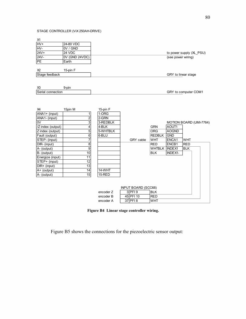
80
STAGE CONTROLLER (ViX 250AH-DRIVE)
X1HV+ 24-80 VDCHV- 0V / GND24V+ 24 VDC to power supply (XL_PSU)24V- 0V (GND 24VDC) (see power wiring)PE Earth
X2 15-pin FGRY to linear stage
X3 9-pin GRY to computer COM1
X4 15pin M 15-pin FANA1+ (input) 1 1-ORGANA1- (input) 2 2-GRN0V 3 3-REDBLK MOTION BOARD (UMI-7764)/Z index (output) 4 4-BLK GRN AOUT1Z index (output) 5 5-WHTBLK ORG AOGNDFault (output) 6 6-BLU REDBLK GNDSTEP- (input) 7 GRY cable WHT ENCA1 WHTDIR- (input) 8 RED ENCB1 REDA- (output) 9 WHTBLK INDEX1 BLKB- (output) 10 BLK INDEX1-Energize (input) 11STEP+ (input) 12DIR+ (input) 13A+ (output) 14 14-WHTA- (output) 15 15-RED
INPUT BOARD (SCC68)encoder Z 3 PFI 9 BLKencoder B 45 PFI 10 REDencoder A 37 PFI 8 WHT
Serial connection
Stage feedback
Figure B4 Linear stage controller wiring.
Figure B5 shows the connections for the piezoelectric sensor output:
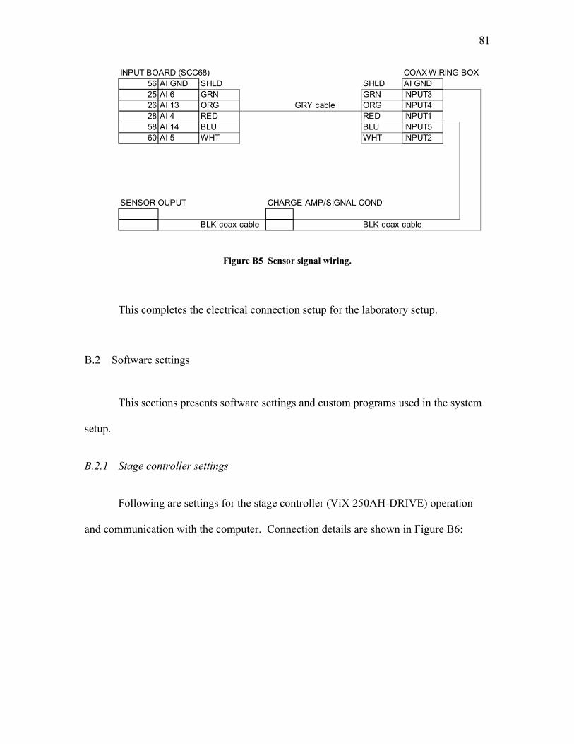
81
INPUT BOARD (SCC68) COAX WIRING BOX56 AI GND SHLD SHLD AI GND25 AI 6 GRN GRN INPUT326 AI 13 ORG GRY cable ORG INPUT428 AI 4 RED RED INPUT158 AI 14 BLU BLU INPUT560 AI 5 WHT WHT INPUT2
SENSOR OUPUT CHARGE AMP/SIGNAL COND
BLK coax cable BLK coax cable
Figure B5 Sensor signal wiring.
This completes the electrical connection setup for the laboratory setup.
B.2 Software settings
This sections presents software settings and custom programs used in the system
setup.
B.2.1 Stage controller settings
Following are settings for the stage controller (ViX 250AH-DRIVE) operation
and communication with the computer. Connection details are shown in Figure B6:
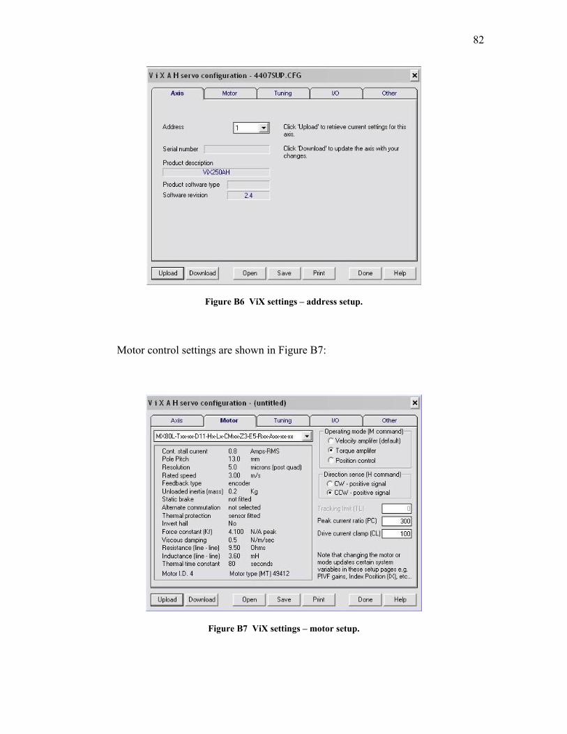
82
Figure B6 ViX settings – address setup.
Motor control settings are shown in Figure B7:
Figure B7 ViX settings – motor setup.
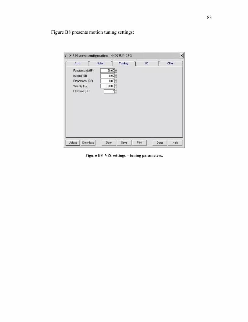
83
Figure B8 presents motion tuning settings:
Figure B8 ViX settings – tuning parameters.

84
Input and output configurations are shown in Figure B9:
Figure B9 ViX settings – input/output setup.
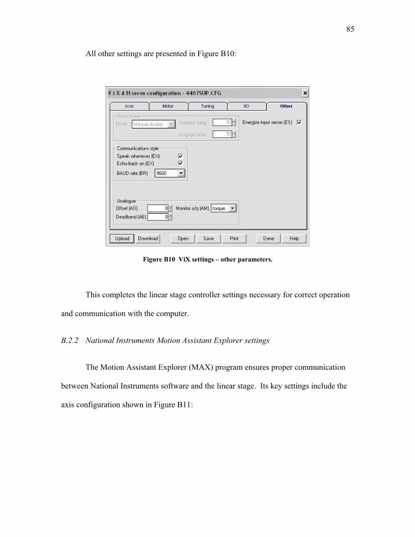
85
All other settings are presented in Figure B10:
Figure B10 ViX settings – other parameters.
This completes the linear stage controller settings necessary for correct operation
and communication with the computer.
B.2.2 National Instruments Motion Assistant Explorer settings
The Motion Assistant Explorer (MAX) program ensures proper communication
between National Instruments software and the linear stage. Its key settings include the
axis configuration shown in Figure B11:

86
Figure B11 Motion Assistant Explorer settings – axis configuration.
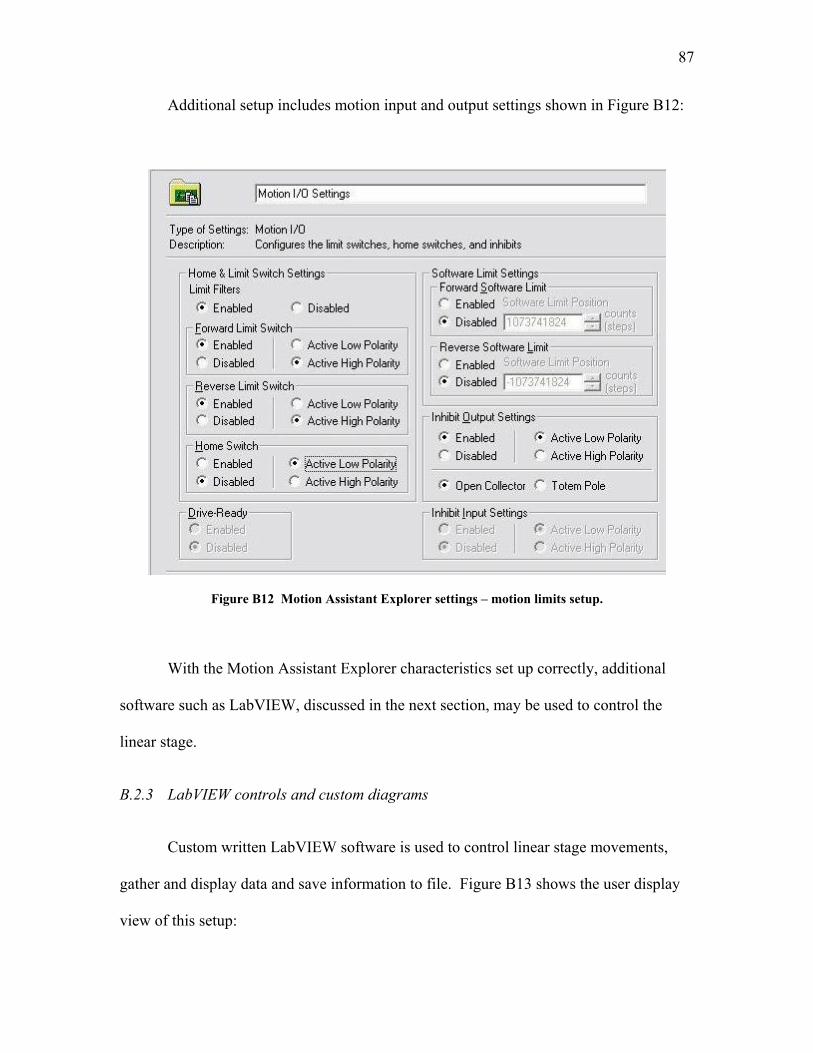
87
Additional setup includes motion input and output settings shown in Figure B12:
Figure B12 Motion Assistant Explorer settings – motion limits setup.
With the Motion Assistant Explorer characteristics set up correctly, additional
software such as LabVIEW, discussed in the next section, may be used to control the
linear stage.
B.2.3 LabVIEW controls and custom diagrams
Custom written LabVIEW software is used to control linear stage movements,
gather and display data and save information to file. Figure B13 shows the user display
view of this setup:
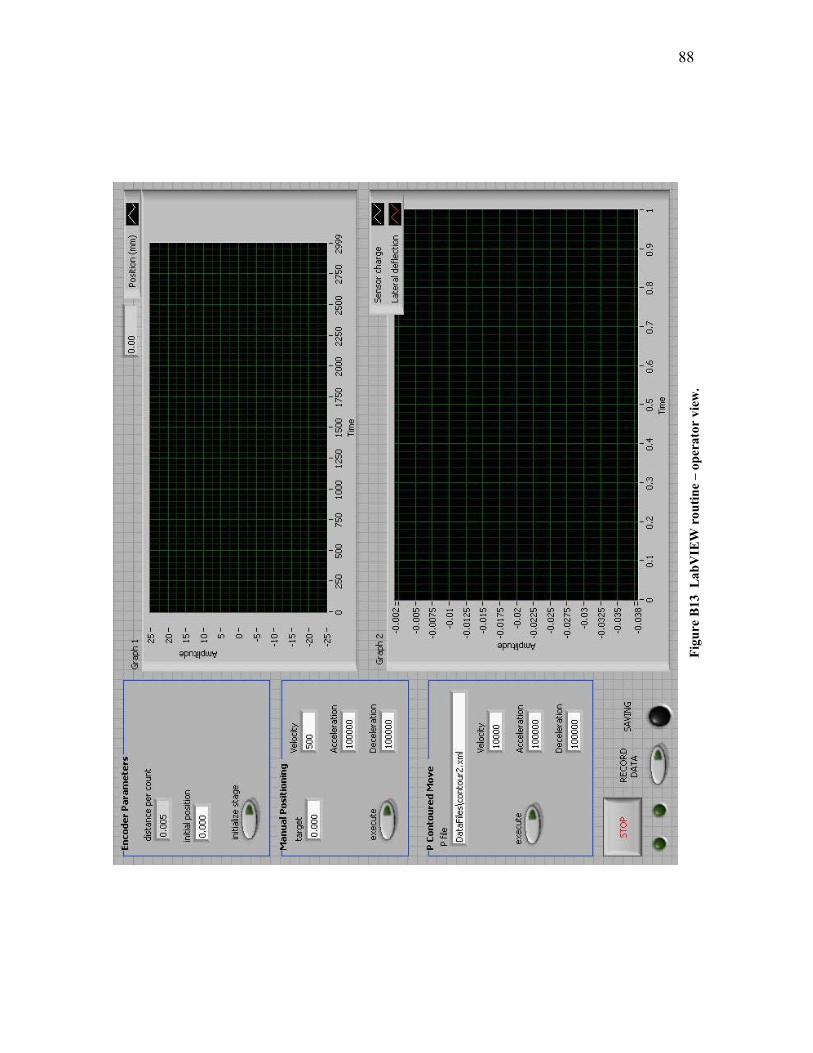
88
Fi
gure
B13
Lab
VIE
W r
outin
e –
oper
ator
vie
w.

89
Custom LabVIEW routines shown in Figure B14 are responsible for gathering
and saving data:

90
Fi
gure
B14
Lab
VIE
W r
outin
e –
initi
aliz
atio
n, d
ata
acqu
isiti
on a
nd fi
le tr
ansf
er.

91
The elements shown in Figure B15 allow for execution of the linear stage
movements:
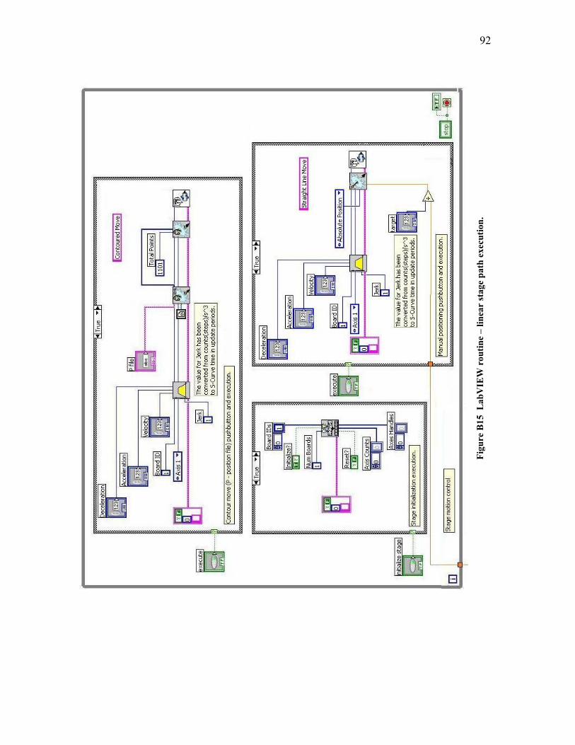
92
Fi
gure
B15
Lab
VIE
W r
outin
e –
linea
r st
age
path
exe
cutio
n.

93
Additional LabVIEW settings used are described in the following section.
B.2.4 LabVIEW settings
Following are LabVIEW input and output settings used within the routine
presented earlier. Figure B16 shows the internal clock setup used for timing of the
feedback signals:
Figure B16 LabVIEW settings – internal clock setup.
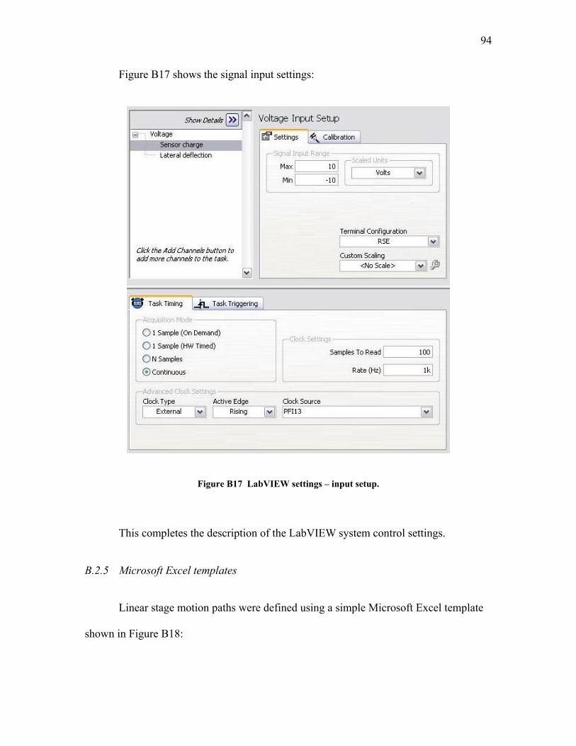
94
Figure B17 shows the signal input settings:
Figure B17 LabVIEW settings – input setup.
This completes the description of the LabVIEW system control settings.
B.2.5 Microsoft Excel templates
Linear stage motion paths were defined using a simple Microsoft Excel template
shown in Figure B18:
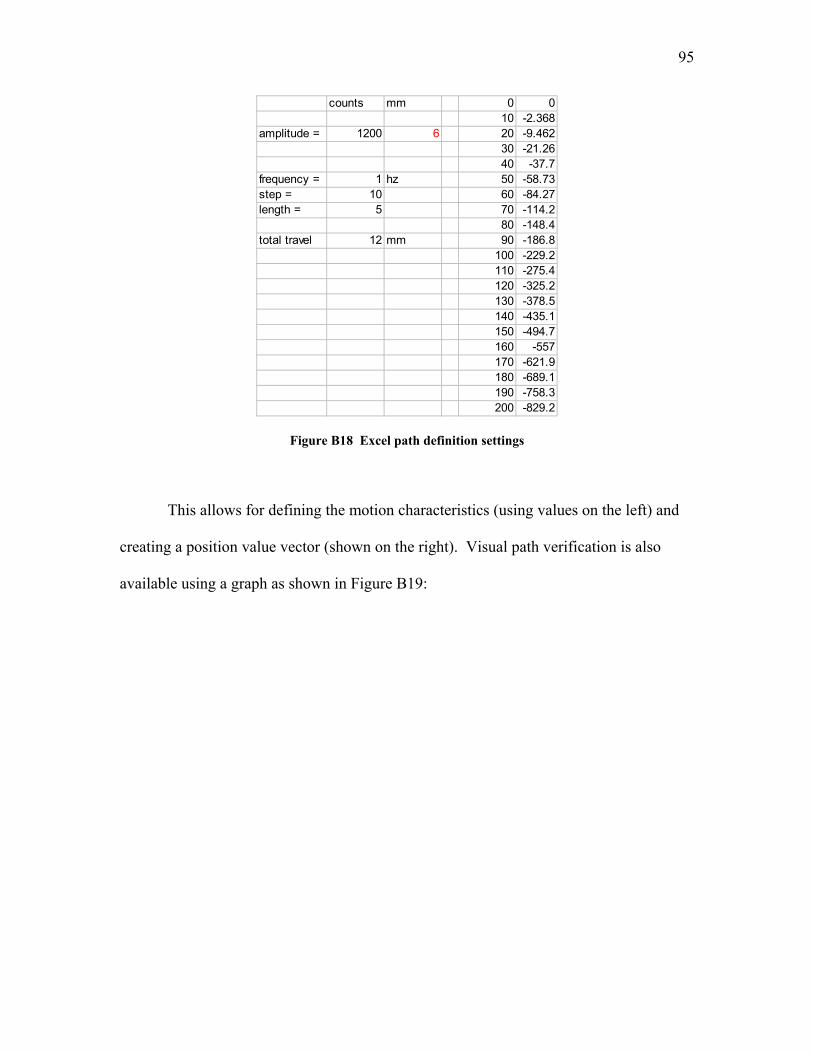
95
counts mm 0 010 -2.368
amplitude = 1200 6 20 -9.46230 -21.2640 -37.7
frequency = 1 hz 50 -58.73step = 10 60 -84.27length = 5 70 -114.2
80 -148.4total travel 12 mm 90 -186.8
100 -229.2110 -275.4120 -325.2130 -378.5140 -435.1150 -494.7160 -557170 -621.9180 -689.1190 -758.3200 -829.2
Figure B18 Excel path definition settings
This allows for defining the motion characteristics (using values on the left) and
creating a position value vector (shown on the right). Visual path verification is also
available using a graph as shown in Figure B19:

96
Position (counts) vs Time (ms)
-3000
-2500
-2000
-1500
-1000
-500
0
500
0 1000 2000 3000 4000 5000 6000 7000 8000 9000 10000
Time (ms)
Posi
tion
(cou
nts)
Figure B19 Path output graph
As discussed earlier in section III.4.1, the data can be then converted into a format
readable by the LabVIEW software for execution of the linear stage motion.
97
VITA
Name:
Bartosz Mika
Address:
c/o: Dr. Hong Liang
Texas A&M University
Department of Mechanical Engineering
TAMU 3123
College Station, TX 77843
Email Address:
Education:
B.S., Mechanical Engineering, University of Washington, 2002
M.S. Mechanical Engineering, Texas A&M University, 2007