Embed Size (px)
Citation preview

7/30/2019 Design and Simulation by Photovoltaic System with Tapped Topology
http://slidepdf.com/reader/full/design-and-simulation-by-photovoltaic-system-with-tapped-topology 1/7
International Journal of Modern Engineering Research (IJMER)
www.ijmer.com Vol.3, Issue.2, March-April. 2013 pp-1238-1244 ISSN: 2249-6645
www.ijmer.com 1238 | Page
Juan C. Yris,1.4
Hugo Calleja G,2
Leobardo H. Gonzalez,3
José A. Olmos1
1(Universidad Juárez Autónoma de Tabasco, Villahermosa, Tabasco, México)
2(Centro de Nacional de Investigación y Desarrollo Tecnológico, Cuernavaca, Morelos. México)
3(ESIME-C Instituto Politécnico Nacional, México, D.F)
4(Instituto Tecnológico Superior de Comalcalco, Tabasco, México)
Abstract: The concept of AC Module is typically applied to transform DC in AC. As a novel solution, center tapped topology is proposed for design of inverter into a Module Integrated Converter (MIC). Main contribution of converter with
tapped inductor topology is to generate a bigger AC voltage to output, depending on the duty cycle and turn ratio of tapped
inductor. The topology chose is convenient because is small, simple and cheap. To achieve a sinusoidal signal output the
inverter is controlled with Sine Pulse Width Modulation (SPWM). The novel converter proposed and its control system is
evaluated by means of the electronic simulator. The simulation results obtained is appreciated that the proposed converter
working in a photovoltaic system increases the voltage gain, increases the efficiency and reduced the harmonic distortion
with respect to traditional converters.
Keywords: Photovoltaic System, tapped Inductor, Module Integrated Converter.
I. INTRODUCTION Traditionally, Photovoltaic systems (PV) installed around the world are grouped in on-grid and off-grid. The first
developed presented greater growth worldwide [1]. They are distinguished by the absence of a storage device, such as
battery. One of its main features is the possibility of improving the quality of service of the energy supplied by the electr ical-
grid. There are three configurations of installation of PV systems that can to be connected to the electrical-grid, are: central
inverter, string inverter and multi-string inverter [2], [3], [4], [5], [6], [7]. An improvement that is achieved in PV system
consists on the implementation of a PV module with a DC-AC converter small or Module Integrated Converter, MIC, the
union of this two is called "AC Module". The AC module easily connects to the electrical-grid under the operate mode of
plug and play. It is suitable for use in powers of 40 to 200W and supports multiple connections in domestic applications with
a maximum theoretical power of 2 kW [8]. Its advantages are: small size, modular and low cost. The main limitation of ACmodule is that MIC power will be equal to the delivered power by the PV module. To improve the delivered power the
converter requires an element that elevates the voltage, such as: Low Frequency Transformer (LFT), High Frequency
Transformer (HFT) and Without Isolation (WI).
The MIC with a conventional inverter uses a LFT in order to obtain electrical isolation between the PV module and
the electrical-grid, as well as raise the low voltage supplied by the DC-AC converter (Fig.1). Its advantage is to have a
simple system and with the disadvantage that it is very heavy. This limits the system to reduce size and weight.
One solution to solve the problem of MIC with a heavy transformer is to use a DC-DC converter with a transformer smaller operating at high frequency (Fig. 2). However, requires two different control circuits with switching processes and losses
higher due to the cascade connection of two power stages.
Another option for high performance is to remove the LFT or HFT (WI), with them the weight is reduced, the price
down, the size is smaller, the arrangement is simple and to obtain a 2% decrease in losses related to HFT [9] this topology is
recommended for power less than 1 kW (Fig. 3).
Fig. 1. MIC with LFT. Fig. 2. MIC with HFT.
Design and Simulation by Photovoltaic System with
Ta ed To olo

7/30/2019 Design and Simulation by Photovoltaic System with Tapped Topology
http://slidepdf.com/reader/full/design-and-simulation-by-photovoltaic-system-with-tapped-topology 2/7
International Journal of Modern Engineering Research (IJMER)
www.ijmer.com Vol.3, Issue.2, March-April. 2013 pp-1238-1244 ISSN: 2249-6645
www.ijmer.com 1239 | Page
Fig. 3. MIC without isolation.
In [10] is presented a converter with the characteristics that must submit as: being small, light-weight and efficient,
its disadvantage is having a low voltage gain. Therefore, it is necessary to develop a DC-DC converter without isolation with
high gain, in order to generate voltage quality in the electrical-grid from a single PV Module (Mark, Conergy C1251P) [11],
with typical output voltage of 14V to 17V, so it is necessary to have a MIC with a large gain to inverter. To do this, it is
established that, it must have a minimum voltage to the inverter input of 180V. To obtain this high voltage is necessary to
have a converter with the ability to raise the voltage, and then you must have a maximum gain of 12.85 for a voltage of 14VDC and a minimum gain of 10.58 in the case of 17V DC. It should be mentioned that the maximum gains obtained in the
traditional conditioner without isolation converters reported do not cover the above needs [12-17].
II. SELECTION OF PROPOSED TOPOLOGY BY DESIGN OF MIC The MIC is divided into several stages of conversion [18]. When the converter is a single stage there are two built-
in functions: firstly developed the conversion of DC-DC with voltage gain and second is developed the inverter (Fig. 4). For
its domestic implementation, is required that the MIC has low weight, high efficiency, high gain and high power density.
Fig. 4. MIC with reduction stages.
The trend in PV conditioners consisting principally of a single stage, with range of efficiency from 87% to 93.26%,
range of switching frequency from 9.6 kHz to 70 kHz. Here are the three alternatives with the best performance gain by
inverter without isolation.
The first inverter analyzed was proposed by Cáceres et al . [12]. It consists of two DC-DC converters type boost,
operating in a complementary mode. However, it has the following disadvantages: low gain, all its transistors operate atHigh Frequency with hard switching technique, the switching loss increases and the system is susceptible to generation
electromagnetic interference.
The second inverter analyzed was proposed by Kusakawa et al . [13], this converter operates with PWM signal and
hard switching technique and control on both sides: on one hand you have the DC-DC conversion and on the other hand the
inverter, it eliminates asymmetry problems. Furthermore, this inverter is appropriate for small power. Its disadvantage is
having a single inductor L to provide the energy for each half cycle of the output voltage; this increases the losses due to
heating.
The third inverter analyzed was proposed by Jain et al [14]. The converter has as function boost and inverts the
waveform of the input voltage. This converter operates with two transistors which operate at high frequency and two
transistors which operate at low frequency. Its reported efficiency is 87% due to losses in the inductors, works in
Discontinuous Conduction Mode operation (DCM) and has implemented tracking Maximum Power Point MPP [19].According to Table 1, the idea development by Jain presents better characteristics as: its higher gain, fewer
components, lower inductance and capacitance and low switching frequency. Based on the reported characteristics by Jain,this proposal is more viable for the purpose of study, which is connected to the electrical-grid a MIC-PV. However, its gain
of 3.6 is not adequate, requires a voltage conversion of 10.58 (minimum). The technique to use to obtain VAC is a
differential connection of the load across the outputs of two converters, Fig.5. Where the converter 1 will produces V1 and

7/30/2019 Design and Simulation by Photovoltaic System with Tapped Topology
http://slidepdf.com/reader/full/design-and-simulation-by-photovoltaic-system-with-tapped-topology 3/7
International Journal of Modern Engineering Research (IJMER)
www.ijmer.com Vol.3, Issue.2, March-April. 2013 pp-1238-1244 ISSN: 2249-6645
www.ijmer.com 1240 | Page
converter 2 will produces V2, the load voltage VO will be given by Vo= V1-V2. While V1 and V2 may both be individually
positive, the voltage across the load can be positive or negative. The converter 1 will operate the positive half cycle of the
AC signal and the converter 2 will operate in the negative half cycle.
III. SELECTION OF DC-CD CONVERTER Of the various existing options to elevation the voltage, there are three viable alternatives for DC/DC converter. In
the Table II are represents the most important characteristics of the three converters above. In it, we can see what is
interesting to explore the tapped-inductor scheme, which while not a new technique has been recently taken [28-31], in order
to obtain higher gain than for traditional converter To develop a DC-DC converter without isolation we have two options
practices: a) traditional with ground output and b) modified without ground output [32]. In the arrangement of a differential
output inverter is necessary that the inverter has without ground output. This characteristic only presented the family the
boost converters. This configuration allows a greater gain than conventional converter. The relationship between the number
of turns of primary (Np) and number of turns of secondary (NS) of tapped-inductor is designated by the letter N (Fig.6).
The variant of converter that presents a better performance when working in two modes of driving is TIST-BB
converter. Which has the advantage of having a duty cycle greater than the others, this is important for control l, because
during the operating cycle of the converter to change the DCM to MCC, through the Case Critical CC.
Table II. - Comparative analysis with the values reported for DC-DC converters without isolation,
Develop variants of Boost Buck (BB) converters modified and are classified according to the bypass element
connected as: Switch to Tap (ST), Diode to Tap (DT), and Rail to Tap (RT), see Fig 7.
Fig. 7. a) Tap-Switch, ST b) Tap-Diode, DT c) Rail-Tap, RT.
7/30/2019 Design and Simulation by Photovoltaic System with Tapped Topology
http://slidepdf.com/reader/full/design-and-simulation-by-photovoltaic-system-with-tapped-topology 4/7
International Journal of Modern Engineering Research (IJMER)
www.ijmer.com Vol.3, Issue.2, March-April. 2013 pp-1238-1244 ISSN: 2249-6645
www.ijmer.com 1241 | Page
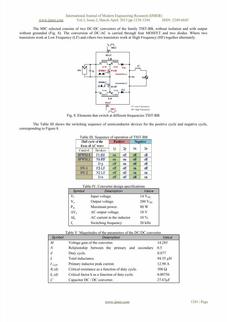
The MIC selected consists of two DC-DC converters of the family TIST-BB, without isolation and with output
without grounded (Fig. 8). The conversion of DC-AC is carried through four MOSFET and two diodes. Where two
transistors work at Low Frequency (LF) and others two transistors work at High Frequency (HF) together alternately.
|
Vo
|
Lf L1-p L2-p
L1-n L2-n
SPWM-1
SPWM-2
Ci
Co
SW-2
SW-1
D-p
D-n
L-p
L-n
P1-HF
N1-HF
VPV
Converter- 2
Converter- 1
N2-LF
P2-LF
LF- Low Frecuency
HF- High Frecuency
Fig. 8. Elements that switch at different frequencies TIST-BB.
The Table III shows the switching sequence of semiconductor devices for the positive cycle and negative cycle,corresponding to Figure 8.
Table III. Sequence of operation of TIST-BB
Table IV. Converter design specifications
Symbol Descripti on Value
Vi Input voltage. 14 VDC
Vo Output voltage. 200 VDC
Pm Maximum power. 80 W
∆Vo AC output voltage. 10 V
∆IL AC current in the inductor 10 %
f s Switching frequency 20 kHz
Table V. Magnitudes of the parameters of the DC/DC converter.
Symbol Description Value
M Voltage gain of the converter. 14.285
N Relationship between the primary and secondary 0.5
d Duty cycle. 0.877
L Total inductance. 94.55 µH
I L1pk Primary inductor peak current. 12.98 A
Rc(d) Critical resistance as a function of duty cycle. 500 Ω
k c (d) Critical factor k as a function of duty cycle. 0.00756
C Capacitor DC / DC converter. 27.67µF

7/30/2019 Design and Simulation by Photovoltaic System with Tapped Topology
http://slidepdf.com/reader/full/design-and-simulation-by-photovoltaic-system-with-tapped-topology 5/7
International Journal of Modern Engineering Research (IJMER)
www.ijmer.com Vol.3, Issue.2, March-April. 2013 pp-1238-1244 ISSN: 2249-6645
www.ijmer.com 1242 | Page
Table VI. Magnitudes of the parameters of the conditioner
Symbol Description Value
M Voltage gain of the conditioner 14.285
N Relationship between the primary and secondary windings 0.5
ma Modulation index 0.877
L Total inductance 94.55 µHCo Output capacitor conditioner 0.44 µF
IV. SIMULATION OF MIC
In Fig. 9 show the waveforms of currents and voltages in the MOSFET and diode, obtained from the PSpice
simulator. For Vi equal to 14VDC, according to design, we obtain a theoretical value of ILpk=12.98A, the simulator gives a
value of 12A. In Fig. 10 are shows the diverse driving modes, DCM, CC and CCM? These changes in driving modes
increased flows in the power devices. Thus, also increases the voltage and current at the converter output TIST-BB.
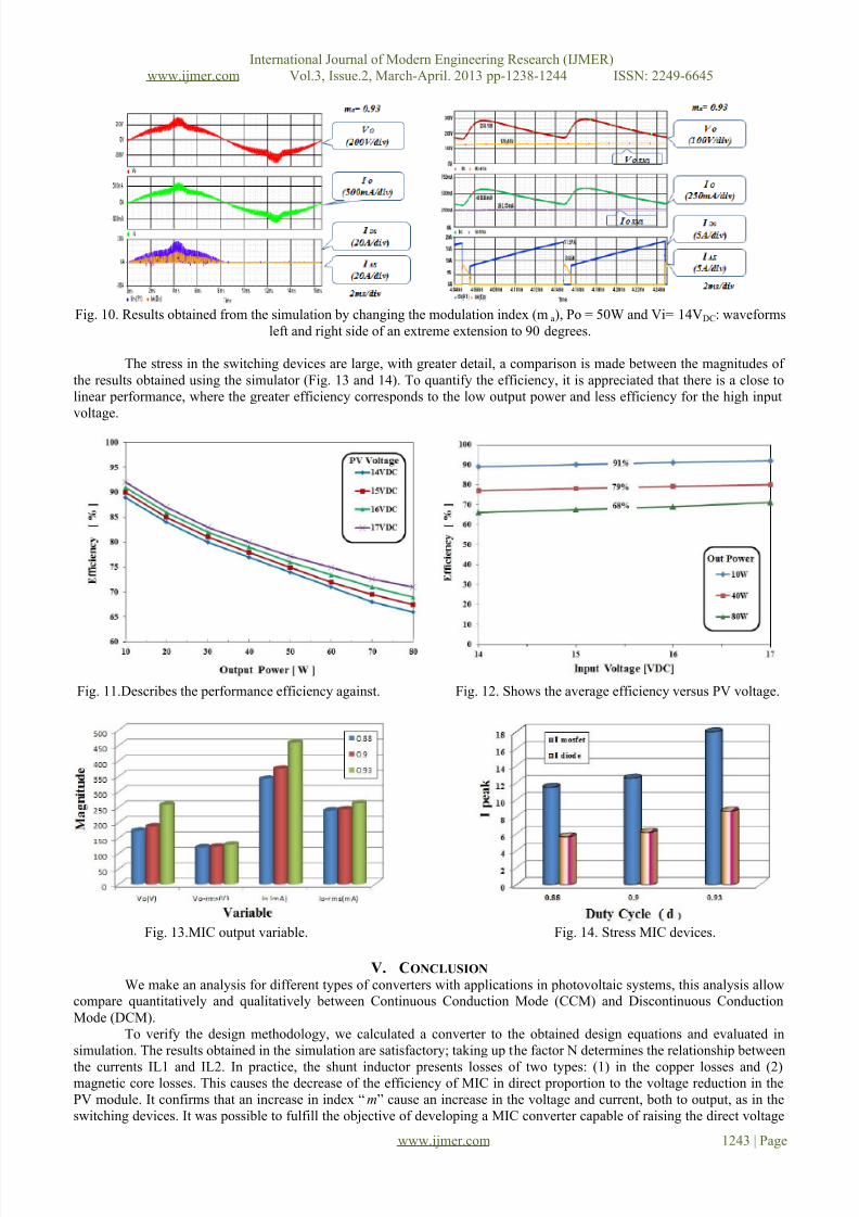
The maximum efficiency is equal to 92% which corresponds to input voltage Vi= 17VDC see Fig. 11. The
performance efficiency has approximately linear behavior. The average efficiency for a 40W power converter is 79% for
input voltage range between 14 to 17 VDC, see Fig. 12. In the converter DC/DC, as power is increased also increases theduty cycle for each value of input voltage in linear form. For example, when working an output power of 80W and d = 0.88
is achieved with input voltage equal to 180 with a input voltage of 14VDC.
Fig. 9. Results of simulation of design prototype.
7/30/2019 Design and Simulation by Photovoltaic System with Tapped Topology
http://slidepdf.com/reader/full/design-and-simulation-by-photovoltaic-system-with-tapped-topology 6/7
International Journal of Modern Engineering Research (IJMER)
www.ijmer.com Vol.3, Issue.2, March-April. 2013 pp-1238-1244 ISSN: 2249-6645
www.ijmer.com 1243 | Page
Fig. 10. Results obtained from the simulation by changing the modulation index (m a), Po = 50W and Vi= 14VDC: waveforms
left and right side of an extreme extension to 90 degrees.
The stress in the switching devices are large, with greater detail, a comparison is made between the magnitudes of
the results obtained using the simulator (Fig. 13 and 14). To quantify the efficiency, it is appreciated that there is a close to
linear performance, where the greater efficiency corresponds to the low output power and less efficiency for the high input
voltage.
Fig. 11.Describes the performance efficiency against. Fig. 12. Shows the average efficiency versus PV voltage.
Fig. 13.MIC output variable. Fig. 14. Stress MIC devices.
V. CONCLUSION We make an analysis for different types of converters with applications in photovoltaic systems, this analysis allow
compare quantitatively and qualitatively between Continuous Conduction Mode (CCM) and Discontinuous Conduction
Mode (DCM).
To verify the design methodology, we calculated a converter to the obtained design equations and evaluated in
simulation. The results obtained in the simulation are satisfactory; taking up the factor N determines the relationship between
the currents IL1 and IL2. In practice, the shunt inductor presents losses of two types: (1) in the copper losses and (2)
magnetic core losses. This causes the decrease of the efficiency of MIC in direct proportion to the voltage reduction in the
PV module. It confirms that an increase in index “m” cause an increase in the voltage and current, both to output, as in the
switching devices. It was possible to fulfill the objective of developing a MIC converter capable of raising the direct voltage

7/30/2019 Design and Simulation by Photovoltaic System with Tapped Topology
http://slidepdf.com/reader/full/design-and-simulation-by-photovoltaic-system-with-tapped-topology 7/7
International Journal of Modern Engineering Research (IJMER)
www.ijmer.com Vol.3, Issue.2, March-April. 2013 pp-1238-1244 ISSN: 2249-6645
www.ijmer.com 1244 | Page
input to an appropriate voltage in the mains. The design methodology allows obtain a prototype MIC with built simple,
compact and lightweight. We conclude that the proposed MIC can be implemented in micro networks, under the concept of
"AC Module"
R EFERENCES [1] Report IEA-PVPS T5-01: Utility Aspects of Grid Connected Photovoltaic Power Systems; 4. AC-MODULE, pp. 4-19.
[2] S.B Kjaer, J.K. Pedersen, F. Blaabjerg, “A review of single-phase grid-connected inverters for photovoltaic modules”, IEEETransactions on Industry Applications, Vol. 41, Issue 5, pp. 1292 – 1306, October 2005.
[3] J. M. A. Myrzik, M. Calais, “String and module integrated inverters for single-phase grid connected photovoltaic systems”, IEEE
Power Tech Conference Proceedings, Bologna, Vol. 2, pp. 8, 23-26, June 2003.
[4] M. Byung-Duk, L. Long-Pil, K. Jong-Hyun, K. Tae-Jin, Y. Dong-Wook, R. Kang-Ryoul, K. Jeong-Joong, S. Eui-Ho, “A NovelGrid-Connected PV PCS with New High Efficiency Converter”, Journal of Power Electronics, Vol. 8, No. 4, pp. 309-316, October 2008.
[5] C. Gyu-Ha, K. Hong-Sung, H. Hye-Seong, J. Byong-Hwan, C. Young-Ho, K. Jae-Chul, “Utility Interactive PV Systems with Power
Shaping Function for Increasing Peak Power Cut Effect”, Journal of Power Electronics, Vol. 8, No. 4, pp. 371-380, October 2008.
[6] L. Jong-Pil, M. Byung-Duk, K. Tae-Jin, Y. Dong-Wook, Y. Ji-Yoon, “Input-Series-Output-Parallel Connected DC/DC Converter for a Photovoltaic PCS with High Efficiency under a Wide Load Range”, Journal of Power Electronics, Vol. 10, No. 1, pp. 9-13,January 2010.
[7] C. Woo-Young, C. Jae-Yeon, “High-Efficiency Power Conditioning System for Grid-Connected Photovoltaic Modules”, Journal of Power Electronics, Vol. 11, No. 4, pp. 561-567, July 2011.
[8] F. Blaabjerg, F. Iov, R. Teodorescu, “Power Electronics in Renewable Energy Systems”; 12th International Power Electronics and
Motion Control Conference, pp. 1 – 17, August 2006.
[9] Chin Quin Yu, Mohan Ned, West Rick and Bonn Russell, “Status and Needs of Power Electronics for Photovoltaic Inverters”,Sandia report SAND 2002-1535, pp. ii – iv. June 2002.
[10] S. B. Kjaer, J. K. Pedersen, F. Blaabjerg; “Power inverter topologies for photovoltaic modules-a review”, Industry ApplicationsConference, Vol. 2, pp. 782-788, 13-18 October 2002.
[11] CONERGY, Photovoltaic C125PI-TD-MEX-0602, www.conergy.com.mx.
[12] R. O. Caceres, I. Barbi, “A boost DC-AC converter: analysis, design, and experimentation”, IEEE Transactions on Power Electronics, Vol. 14, Issue 1, pp. 134 – 141, January 1999.
[13] H. Kusakawa, H. Nagayoshi; K. Kamisako, K. Kurahaura, “Further improvement of a transformerless voltage -boosting inverter for ac modules”, Solar Energy Material and Solar Cells, Vol. 67, pp. 379-387, March 2001.
[14] N, Kasa, T. Iida, “Flyback type inverter for small scale photovoltaic power system”, 28th Annual Conference of the Industrial
Electronics Society IECON, Vol. 2, pp.1089-1094, 2002.[15] W. Chien-Ming, C. Huang-Jen, “A novel single-stage half-bridge series-resonant buck- boost inverter”, The Fifth International
Conference on Power Electronics and Drive Systems, PEDS, Vol. 2, pp. 1307-1312, November 2003.
[16] W. Chien-Ming; “A Novel Single-Stage Series-Resonant Buck – Boost Inverter, IEEE Transactions on Industrial Electronics”, Vol. 52,
Issue 4, pp. 1099 – 1108, August 2005.[17] S. Jain, V. Agarwal, “A Single-Stage Grid Connected Inverter Topology for Solar PV Systems with Maximum Power Point
Tracking”, IEEE Transactions on Power Electronics, Vol. 22, Issue 5, pp. 1928 – 1940, Sep. 2007.
[18] S. Saha, N. Matsui, V.P. Sudarsingh, “Design of a low power utility interactive photovoltaic inverter”; International Conference onPower Electronic Drives and Energy Systems for Industrial Growth, Vol. 1, pp.481 – 4871, 1998.
[19] T. Esram, P.L. Chapman, “Comparison of Photovoltaic Array Maximum Power Point Tracking Techniques”; IEEE Transaction onEnergy Conversion, Vol. 22, Issue 2, pp. 439 – 449, June 2007.
[20] Z. Qun, F. C. Lee, “High performance coupled-inductor DC-DC converters”, Eighteenth Annual Applied Power Electronics
Conference and Exposition, Vol. 1, pp. 109-1139, 2003[21] K. C. Tseng, T. J. Liang, “Novel high-efficiency step-up converter”; IEE Proceedings Electric Power Applications, Vol. 151, Issue
2, pp. 182 – 190, March 2004.
[22] T. J. Liang, K. C. Tseng; “Analysis of integrated boost-flyback step-up converter”; IEE Proceedings Electric Power Applications,Vol. 152, Issue 2, pp. 217 – 225, March 2005.
[23] S. Malo, R. Grino, “Output Voltage Regulation of a High -Efficiency High Step-Up DC-DC Power Converter”; IEEE International
Symposium Industrial Electronics, ISIE 2007. pp. 854 – 859, June 2007.
[24] B. Ju-Won, R. Myung-Hyo, K. Tae-Jin, Y. Dong-Wook, K. Jong-Soo, “High boost converter using voltage multiplier”; 31st AnnualConference on Industrial Electronics Society, IECON 2005, pp. 567-5726, November 2005.
[25] K. W. E Cheng, “Tapped inductor for switched-mode power converters”; Power Electronics systems and Applications; ICPESA '06, pp. 14 – 20, 2006.
[26] D. A. Grant, Y. Darroman, J. Suter, “Synthesis of Tapped-Inductor Switched-Mode Converters”; IEEE Transactions on Power
Electronics, Vol. 22, Issue 5, pp. 1964 – 1969, 2007.
[27] J. P. Fohringer, F. A. Himmelstoss, “Analysis of a boost converter with tapped inductor and reduced voltage stress across the buffer capacitor”; IEEE International Conference Industrial Technology ICIT, pp. 126 – 131, December 2006.
[28] S. V. Araujo, P. Zacharias, B. Sahan, R. P. Torrico Bascope, F. Antunes, V. Araújo, S. Z. Peter; R. Bascope-Torrico; A. Fernando
L.M; “Analysis and proposition of a PV module integrated converter with high voltage gain capability in a non -isolated topology”;
7th International conference on Power Electronics EXCO Daegu, Korea, pp. 511-517, October 2007.[29] S. V. Araùjo, P. Zacharias, B. Sahan, “Novel Grid -Connected Non-Isolated Converters for Photovoltaic Systems with Grounded
Generator”; 39th IEEE Annual Power Electronics Specialists Conference, PESC, pp. 58-65, June 2008.
[30] H. Cheng, K. M. Smedley, A. Abramovitz; “A Wide-Input-Wide-Output (WIWO) DC –DC Converter”; IEEE Transactions on Power
Electronics, Vol. 25, No.2, pp. 280-289, February 2010.[31] B. Yang, W. Li, Y. Zhao, X. He, “Design and Analysis of a Grid-Connected Photovoltaic Power System”; IEEE Transactions on
Power Electronic, Vol. 25 No.4, pp. 992-1000, April 2010.
[32] L. F. Lin, Advance DC/DC converters-power electronic and applications series; CRC Press LLC .www.crcpress.com.


![An Efficient Bridge-Less Power Factor Correction Tapped ... · Cuk converter topology is generally a converter with lesser efficiency, ... TI-flyback [12], TI-cascaded boost [12];](https://img.dokumen.tips/doc/110x75/5b019fb47f8b9a84338e6c9c/an-efficient-bridge-less-power-factor-correction-tapped-converter-topology-is.jpg)