Embed Size (px)
Citation preview
International Research Journal of Engineering and Technology (IRJET) e-ISSN: 2395 -0056
Volume: 04 Issue: 04 | April-2017 www.irjet.net p-ISSN: 2395-0072
© 2017, IRJET | Impact Factor value: 5.181 | ISO 9001:2008 Certified Journal | Page 1535
Design and Modeling of Substrate Integrated Waveguide based
Antenna to Study the Effect of Different Dielectric Materials
Jagmeet Kour1, Gurpadam Singh1, Sandeep Arya2
1Department of Electronics and Communication Engineering, Beant College of Engineering & Technology,
Gurdaspur, Punjab-143521, India 2Department of Physics & Electronics, University of Jammu, Jammu, J&K-180002, India
---------------------------------------------------------------------***---------------------------------------------------------------------
Abstract - In this paper, antenna models of substrate integrated waveguide (SIW) has been analyzed and designed to investigate the effect of dielectric materials on its operating parameters. Parameters that have been evaluated in this work are electric field, return losses, bandwidth and the transmission gain. Printed circuit board (PCB), Silicon (Si) and Mica are used as different dielectrics to evaluate the results in the frequency domain between 6 to 11 GHz. Design steps in an orderly manner were pursued for the optimization of geometrical dimensions followed by the finite-element method (FEM) based modeling of the SIW structure. The results obtained had shown that the transmission is possible for all the three cases but the optimized results were observed for Silicon as dielectric substrate.
Key Words: Substrate Integrated Waveguide, insertion loss, cylindrical vias, microstrip line.
1. INTRODUCTION
The amelioration in mm-wave technologies is consequential for the development of wireless systems as broadband and high resolution techniques are held up by the utilization of mm-waves. In the majority of these systems, the accomplishment of this technology largely depends on the accessibility of a cost-effectual technology, felicitous for the mass-engenderment of components and systems. It is prognosticable that high-density amalgamation techniques, cumulated with a low-cost manufacture process, be supposed to be able to present widespread solutions for mm-wave commercial applications. The nucleus of these systems is cognate to the active part, which includes components such as local oscillators, mixers and possibly low-noise amplifiers among others. Now-a-days, such components can be incorporated in the outward appearance of chip-sets at plausibly low cost. A number of semiconductor companies are at present running towards the enlargement of chip-sets working at 45 GHz or even at higher frequencies [1]. On the other hand, incipient components are desirable in mm-wave systems, which cannot be expediently incorporated in the chip-set, because either they are too astronomically immense or the required performance cannot be achieved by integrated components (such as antennas, selective filters and power amplifiers). These adscititious components could be simply considered
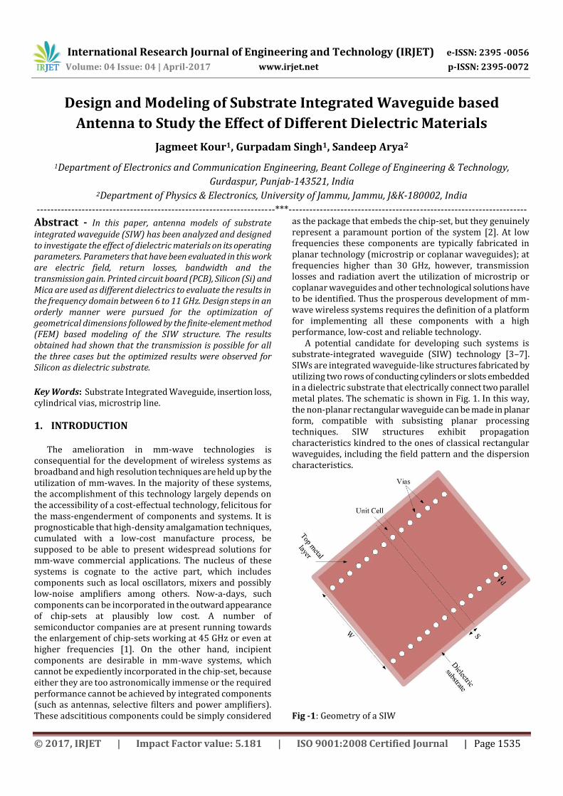
as the package that embeds the chip-set, but they genuinely represent a paramount portion of the system [2]. At low frequencies these components are typically fabricated in planar technology (microstrip or coplanar waveguides); at frequencies higher than 30 GHz, however, transmission losses and radiation avert the utilization of microstrip or coplanar waveguides and other technological solutions have to be identified. Thus the prosperous development of mm-wave wireless systems requires the definition of a platform for implementing all these components with a high performance, low-cost and reliable technology. A potential candidate for developing such systems is substrate-integrated waveguide (SIW) technology [3–7]. SIWs are integrated waveguide-like structures fabricated by utilizing two rows of conducting cylinders or slots embedded in a dielectric substrate that electrically connect two parallel metal plates. The schematic is shown in Fig. 1. In this way, the non-planar rectangular waveguide can be made in planar form, compatible with subsisting planar processing techniques. SIW structures exhibit propagation characteristics kindred to the ones of classical rectangular waveguides, including the field pattern and the dispersion characteristics.
Fig -1: Geometry of a SIW

International Research Journal of Engineering and Technology (IRJET) e-ISSN: 2395 -0056
Volume: 04 Issue: 04 | April-2017 www.irjet.net p-ISSN: 2395-0072
© 2017, IRJET | Impact Factor value: 5.181 | ISO 9001:2008 Certified Journal | Page 1536
Moreover, SIW structures preserve most of the advantages of conventional metallic waveguides, namely high quality-factor and high power-handling capability with self-consistent electrical shielding. The most paramount advantage of SIW technology is the possibility to integrate all the components on the same substrate, including passive components, active elements and even antennas. Moreover, there is the possibility to mount one or more chip-sets on the same substrate. There is no desideratum for transitions between elements fabricated with different technologies, thus reducing losses and parasitics. In this work the structure of basic SIW is altered and the performance of the simulated antennas are evaluated for three different dielectric materials.
2. MATHEMATICAL ANALYSIS SIW can be modeled as a Rectangular waveguide (RW) as shown in Fig. 2. Generally, a rectangular waveguide has horizontal length of a and vertical length of b and its cut-off frequency is determined by a and b.
a
ɛr adb
Fig -2: Dimensions for SIW
Since the length of vertical wall of SIW becomes height of substrate, h and horizontal length a is much longer than height of substrate (a≫ b=h), the cutoff frequency of the SIW is given by:
2 21
2 2
k m nf
a b
(i)
Thus, 10
1
2f
a (ii)
If ad is the width of SIW, then the width of the substrate can be determined as
d
R
aa
(iii)
where R is the relative permittivity.
The distance between opposite via of the SIW is given by [8]
2
0.95s d
da a
p (iv)
where d is the diameter of the via, p is pitch (distance between the vias).
The guided wavelength in the SIW is given by following formula [9]
22
2
2
(2 )g
R f
ac
(v)
Where f is the resonant frequency, c is the speed of electromagnetic wave in free space and a is the width of the waveguide. The distance between two arrays determines the propagation constant of the fundamental mode, and the via apertures parameters (d and p) are set to minimize the radiation loss as well as the return loss. In order to insure that the synthesized waveguide section become radiation less or free of leakage loss, parametric effect of p and d can be studied [20]. These studies reveal that the pitch must be kept minuscule to reduce the loss between adjacent points.
3. SIW ANTENNA DESIGN Figure 3 shows the designed structure of an SIW consisting of the top and bottom planes of a substrate and two parallel via fences in the substrate. The via are composed such that only patterns with vertical current distributed on the side wall can survive in SIWs.
(a) (b)
Fig -3: Structure of designed SIW (a) 2D design (b) 3D design
The current path will not be cut by via fences, therefore TE10 mode can be supported in an SIW. This holds for all TEm0 modes since their current distributions on the side walls are similar. On the other hand, horizontal components of the surface current exist on the sidewalls for all TM modes and TEmn modes with nonzero n’s. These current paths will be cut in SIW structures, which results in radiation. Therefore we can conclude that only TEm0 modes exist in SIW structures [12]. Different substrates have been taken for this experiment to find their effect on the propagation patterns of SIWs. Table 1 shows different materials taken as substrate along with their properties.

International Research Journal of Engineering and Technology (IRJET) e-ISSN: 2395 -0056
Volume: 04 Issue: 04 | April-2017 www.irjet.net p-ISSN: 2395-0072
© 2017, IRJET | Impact Factor value: 5.181 | ISO 9001:2008 Certified Journal | Page 1537
Table -1: Properties of different dielectric materials
Materials
Relative Permittivity
Relative
Permeability
Electrical
Conductivity
PCB
3.38
1
0
Silicon
11.7
1
1 x 10-12
Mica
6
1
2 x 10-15
The models were designed using electromagnetic, frequency domain solver. A range of frequency from 6 GHz to 11 GHz is applied through the lumped ports to analyze the results for different SIW designs.
4. RESULTS AND DISCUSSIONS Fig. 4(a) shows the meshing design of a micro-cantilever model. The whole structure is enclosed in the spherical domain as shown in Fig. 4(b) to evaluate the antenna performance. Normal meshing is conducted on the SIW structure. The maximum element size selected is 0.00375. The design was simulated on the computational machine having 3.4 GHz processor speed. The virtual memory used while simulation was 2.97 GB. Normal meshing is selected to reduce the computational load.
Fig -4(a): SIW structure while meshing is applied
Fig -4(b): SIW based antenna enclosed in spherical domain
The electric field generated while computing the results for different substrates are shown in figure 5. Fig. 5(a) shows the simulated result for electric field for PCB as substrate, while fig. 5(b) and 5(c) shows the radiations due to electric field generated for substrates taken as Silicon and Mica respectively.
Fig -5(a): Electric field for PCB substrate
Fig -5(b): Electric field for Mica substrate
Fig -5(c): Electric field for Silicon substrate

International Research Journal of Engineering and Technology (IRJET) e-ISSN: 2395 -0056
Volume: 04 Issue: 04 | April-2017 www.irjet.net p-ISSN: 2395-0072
© 2017, IRJET | Impact Factor value: 5.181 | ISO 9001:2008 Certified Journal | Page 1538
From the bar line adjacent to these graphs it is clear that the maximum value (1.6 KV/m) of electric field is for PCB while for minimum value (700 V/m) is for silicon. For Mica, the maximum value of electric field is 1.0 KV/m. Similarly the plot shown in figure 6 indicates graph between S-parameters and the frequency.
Fig -6(a): S-parameter for PCB substrate
Fig -6(b): S-parameter for Mica substrate
Fig -6(c): S-parameter for Silicon substrate
Return losses or input reflection coefficient (S11) and the forward transmission gain (S21) were plotted for all the dielectric material used as a substrate in the experiment. Fig. 6(a) shows the S11 and S21 parameter w. r. t. frequency plot for PCB. Dip in the return loss is observed at 9.3 GHz and transmission gain increases upto 9.3 GHz and then decreases. Similarly, return loss and transmission gain for mica and silicon are also plotted in Fig. 6(b) and 6(c) respectively. In case of silicon, return loss showed a main dip at frequency 6.6 GHz, while transmission gain is negligibly small. Mica substrate used in the simulation showed increase in the transmission gain upto a frequency from 6 GHz to 8.5 GHz. Unity transmission gain is obtained from 8.5 GHz to 11 GHz. Dip in the return loss of -26dB is seen at frequency of 9.0 GHz. Fig. 7 shows the radiation pattern obtained while evaluation of results.
Fig -7(a): Radiation pattern for PCB substrate
Radiation Pattern
Fig -7(b): Radiation pattern for Mica substrate

International Research Journal of Engineering and Technology (IRJET) e-ISSN: 2395 -0056
Volume: 04 Issue: 04 | April-2017 www.irjet.net p-ISSN: 2395-0072
© 2017, IRJET | Impact Factor value: 5.181 | ISO 9001:2008 Certified Journal | Page 1539
Fig -7(c): Radiation pattern for Silicon substrate
The results show that the simulated design comes with a subsequent gain for the entire frequency band especially at resonance. However the gain is better for the antenna with PCB as substrate.
5. CONCLUSIONS Simulation work is carried out to investigate the effect of different dielectric substrates on the electromagnetic wave propagation in SIW. To evaluate the effect of dielectric material, three different substrates such as PCB, mica, and silicon were used in the experiment. S-parameters such as return loss and transmission gain were calculated for frequency ranging from 6 GHz to 11 GHz. Table 2 shows the comparative analysis of the results obtained for all the three different dielectrics based antenna. Table -1: Properties of different dielectric materials
Materials Electric Field
Bandwidth Resonant Frequency
Frequency Range
Gain
PCB 1.7 KV/m 200 MHz 9.3 GHz 9.2 GHz to 9.4 GHz
2.3 dB
Silicon 700 V/m 500 MHz 6.6 GHz 6.3 GHz to 6.8 GHz.
0.75 dB
Mica 1 KV/m 1200 MHz 9.0 GHz 8.5 GHz to 9.7 GHz
0.95 dB
From the table 2, it can be estimated that PCB substrate based SIW antenna shows better results than the other two dielectric antennas. It can be concluded that the SIW works efficiently at around 9.3 GHz wih better output parameters. REFERENCES [1] A. M. Niknejad, H. Hashemi, Millimetre-wave silicon
technology: 60 GHz and beyond, Springer, 2008.
[2] M. P. Gaynor, System-in-package RF design and applications’, Artech House, 2007.
[3] J. Hirokawa, M. Ando, “Single-layer feed waveguide consisting of posts for plane TEM wave excitation in parallel plates,” IEEE Trans. Antennas Propag., vol. 46, 1998, pp. 625–630.
[4] U. Hiroshi, T. Takeshi, M. Fujii, “Development of a laminated waveguide,” IEEE Trans. Microw. Theory Techn., vol. 46, 1998, pp. 2438–2443.
[5] D. Deslandes, K. Wu, “Single-substrate integration technique of planar circuits and waveguide filters,” IEEE Trans. Microw. Theory Tech., vol. 51, 2003, pp. 593–596.
[6] F. Xu, K. Wu, “Guided-wave and leakage characteristics of substrate integrated waveguide,” IEEE Trans. Microw. Theory Tech., vol. 53, 2005, pp. 66–73.
[7] D. Deslandes, K. Wu, “Accurate modeling, wave mechanisms, and design considerations of a substrate integrated waveguide,” IEEE Trans. Microw. Theory Tech., vol. 54, 2006, pp. 2516–2526.
[8] K. Wu, “Towards system-on-substrate approach for future millimeterwave and photonic wireless applications,” Proc. Asia-Pacific Microwave Conf., 2006.


![Introduction - Wiley€¦ · Introduction A coplanar waveguide (CPW) fabricated on a dielectric substrate was Þrst demonstrated by C. P. Wen [1] in 1969. Since that time, tremendous](https://img.dokumen.tips/doc/110x75/5f029e577e708231d40529d7/introduction-wiley-introduction-a-coplanar-waveguide-cpw-fabricated-on-a-dielectric.jpg)