Embed Size (px)
Citation preview
DESIGN AND IMPLEMENTATION OF COUPLED INDUCTOR CUK
CONVERTER OPERATING IN CONTINUOUS CONDUCTION MODE
A THESIS SUBMITTED TO
THE GRADUATE SCHOOL OF NATURAL AND APPLIED SCIENCES
OF
MIDDLE EAST TECHNICAL UNIVERSITY
BY
MUSTAFA TUFAN AYHAN
IN PARTIAL FULLFILLMENT OF THE REQUIREMENTS
FOR
THE DEGREE OF MASTER OF SCIENCE
IN
ELECTRICAL AND ELECTRONICS ENGINEERING
DECEMBER 2011

Approval of the thesis:
DESIGN AND IMPLEMENTATION OF COUPLED INDUCTOR CUK
CONVERTER OPERATING IN CONTINUOUS CONDUCTION MODE
submitted by MUSTAFA TUFAN AYHAN in partial fulfillment of the
requirements for the degree of Master of Science in Electrical and Electronics
Engineering Department, Middle East Technical University by,
Prof. Dr. Canan ÖZGEN
Dean, Graduate School of Natural and Applied Sciences
Prof. Dr. İsmet ERKMEN
Head of Department, Electrical and Electronics Engineering
Prof. Dr. Aydın ERSAK
Supervisor, Electrical and Electronics Engineering Dept., METU
Examining Committee Members:
Prof. Dr. Muammer ERMİŞ
Electrical and Electronics Engineering Dept., METU
Prof. Dr. Aydın ERSAK
Electrical and Electronics Engineering Dept., METU
Prof. Dr. Işık ÇADIRCI
Electrical and Electronics Engineering Dept., HU
Dr. Faruk BİLGİN
Space Technologies Research Institute, TÜBİTAK
Özgür YAMAN, M.Sc.
REHİS, ASELSAN
Date: 09.12.2011

iii
I hereby declare that all information in this document has been obtained and
presented in accordance with academic rules and ethical conduct. I also
declare that, as required by these rules and conduct, I have fully cited and
referenced all material and results that are not original to this work.
Name, Last name : Mustafa Tufan AYHAN
Signature :
iv
ABSTRACT
DESIGN AND IMPLEMENTATION OF COUPLED
INDUCTOR CUK CONVERTER OPERATING IN
CONTINUOUS CONDUCTION MODE
AYHAN, Mustafa Tufan
M. Sc., Department of Electrical and Electronics Engineering
Supervisor: Prof. Dr. Aydın ERSAK
December 2011, 253 pages
The study involves the following stages: First, coupled-inductor and integrated
magnetic structure used in Šuk converter circuit topologies are analyzed and the
necessary information about these elements in circuit design is gathered. Also,
benefits of using these magnetic elements are presented. Secondly; steady-state
model, dynamic model and transfer functions of coupled-inductor Šuk converter
topology are obtained via state-space averaging method. Third stage deals with
determining the design criteria to be fulfilled by the implemented circuit. The
selection of the circuit components and the design of the coupled-inductor
providing ripple-free input current waveform are performed at this stage. Fourth
stage introduces the experimental results of the implemented circuit operating in
open loop mode. Besides, the controller design is carried out and the closed loop
performance of the implemented circuit is presented in this stage.
Keywords: Šuk converter, coupled-inductor, integrated magnetic structure, state-
space averaging method

v
ÖZ
SÜREKLİ İLETİM KİPİNDE ÇALIŞAN BAĞLAŞIK
İNDÜKTÖRLÜ CUK ÇEVİRİCİ TASARIMI VE
GERÇEKLENMESİ
AYHAN, Mustafa Tufan
Yüksek Lisans, Elektrik Elektronik Mühendisliği Bölümü
Tez Yöneticisi: Prof. Dr. Aydın ERSAK
Aralık 2011, 253 sayfa
Bu çalışma şu aşamaları içermektedir: İlk olarak, Šuk çevirici topolojilerinde
kullanılan bağlaşık indüktör ve bütünleşmiş manyetik yapı analiz edilmektedir ve
bu elemanlarla ilgili devre tasarımında gerekli olan bilgiler derlenmektedir. Ayrıca,
bu manyetik elemanları kullanmanın sağladığı yararlar sunulmaktadır. İkinci olarak,
durum uzayı ortalama metodu kullanılarak bağlaşık indüktörlü Šuk çevirici
topolojisine ait kararlı durum modeli, dinamik model ve transfer fonksiyonlar elde
edilmektedir. Üçüncü aşama, gerçeklenecek devrenin yerine getirmesi gereken
tasarım kıstaslarının tespitinden bahsetmektedir. Devre elemanlarının seçimi ve
kıpırtısız giriş akım dalga formu sağlayan bağlaşık indüktörün tasarımı bu aşamada
gerçekleştirilmektedir. Dördüncü aşama, gerçeklenen devrenin açık döngü kipinde
çalışırkenki deneysel sonuçlarını ortaya koymaktadır. Ayrıca bu aşamada,
denetleyici tasarımı gerçekleştirilmektedir ve gerçeklenen devrenin kapalı döngü
performansı sunulmaktadır.
Anahtar Kelimeler: Šuk çevirici, bağlaşık indüktör, bütünleşmiş manyetik yapı,
durum uzayı ortalama metodu

vi
To My Fiancée
And
Our Beloved Families

vii
ACKNOWLEDGEMENTS
I would like to express my gratitude to my supervisor Prof. Dr. Aydın ERSAK for
his guidance, advice, criticism, encouragement and insight throughout the
completion of the thesis.
I am indebted to all of my friends and colleagues for their support and
encouragements. I am also grateful to ASELSAN Inc. for the facilities that made
my work easier and TÜBİTAK for the scholarship that supported my work.
Finally I am grateful to my family together with my fiancée and her family for their
continuous support and encouragements.

viii
TABLE OF CONTENTS
ABSTRACT ................................................................................................................................ IV
ÖZ ................................................................................................................................................ V
ACKNOWLEDGEMENTS .......................................................................................................VII
TABLE OF CONTENTS ......................................................................................................... VIII
LIST OF TABLES ...................................................................................................................... XI
LIST OF ABBREVIATIONS .................................................................................................. XXI
NOMENCLATURE ................................................................................................................ XXII
CHAPTERS
1. INTRODUCTION..................................................................................................................... 1
1.1 HISTORY ............................................................................................................................ 1
1.2 THESIS ORGANIZATION .................................................................................................. 2
1.3 CONTRIBUTIONS OF THESIS ........................................................................................... 3
2. MATHEMATICAL ANALYSIS OF MAGNETIC ELEMENTS IN CUK CONVERTER
TOPOLOGIES ............................................................................................................................. 6
2.1 INTRODUCTION ................................................................................................................ 6
2.2 ANALYSIS OF COUPLED-INDUCTOR ............................................................................. 7
2.2.1 Analysis of Ideal Model ................................................................................................ 7
2.2.2 Merits of Coupling ...................................................................................................... 14
2.2.3 Analysis of Parasitic Model ......................................................................................... 31
2.3 ANALYSIS OF INTEGRATED MAGNETIC STRUCTURE .............................................. 40
2.3.1 Analysis of Ideal Model and Merits of Coupling .......................................................... 41
3. STEADY-STATE AND DYNAMIC MODEL ANALYSIS.................................................... 62
3.1 INTRODUCTION .............................................................................................................. 62
3.2 STATE-SPACE AVERAGING METHOD.......................................................................... 62
3.3 ANALYSIS OF COUPLED-INDUCTOR ŠUK CONVERTER, CIŠC WITH IDEAL
ELEMENTS ............................................................................................................................ 66
3.3.1 State-Space Equation Set in Mode 1 ............................................................................ 67
3.3.2 State-Space Equation Set in Mode 2 ............................................................................ 69

ix
3.3.3 Averaging of Matrices in Mode 1 and Mode 2 ............................................................. 71
3.3.4 Decomposition of Averaged Model into Steady-State and Dynamic Models ................. 72
3.3.5 Steady-State Model ..................................................................................................... 74
3.3.6 Dynamic Model and Transfer Functions ...................................................................... 77
3.3.7 Verification of the Transfer Functions ......................................................................... 81
3.4 ANALYSIS OF COUPLED-INDUCTOR ŠUK CONVERTER WITH PARASITIC
ELEMENTS ............................................................................................................................ 92
3.4.1 State-Space Equation Set in Mode 1 ............................................................................ 92
3.4.2 State-Space Equation Set in Mode 2 ............................................................................ 95
3.4.3 Averaging of Matrices in Mode 1 and Mode 2 ............................................................. 98
3.4.4 Decomposition of Averaged Model into Steady-State and Dynamic Models ................. 99
3.4.5 Steady-State Model ................................................................................................... 101
3.4.6 Dynamic Model and Transfer Functions .................................................................... 104
3.4.7 Verification of the Transfer Functions ....................................................................... 109
4. DESIGN OF A COUPLED-INDUCTOR CUK CONVERTER........................................... 119
4.1 INTRODUCTION ............................................................................................................ 119
4.2 OPERATIONAL REQUIREMENTS OF THE CONVERTER ........................................... 119
4.3 SELECTION AND DESIGN OF THE CIRCUIT COMPONENTS .................................... 130
4.3.1 Selection of MOSFET ............................................................................................... 130
4.3.2 Selection of Diode ..................................................................................................... 134
4.3.3 Selection of .......................................................................................................... 136
4.3.4 Selection of .......................................................................................................... 142
4.3.5 Design of Coupled-Inductor ...................................................................................... 147
5. CONTROLLER DESIGN .................................................................................................... 175
5.1 INTRODUCTION ............................................................................................................ 175
5.2 CONTROL BLOCK DIAGRAM ...................................................................................... 178
5.3 CONTROLLER DESIGN ................................................................................................. 179
5.3.1 Controller Design of the Current Loop ....................................................................... 180
5.3.2 Controller Design of the Voltage Loop ...................................................................... 187
5.4 DOMAIN CONVERSIONS .............................................................................................. 192
5.5 APPLICATION SPECIFIC POINTS ................................................................................. 194
6. EXPERIMENTAL RESULTS .............................................................................................. 197
6.1 INTRODUCTION ............................................................................................................ 197
6.2 OPEN-LOOP RESULTS .................................................................................................. 199
6.2.1 Voltage Waveforms .................................................................................................. 199
6.2.2 Current Waveforms ................................................................................................... 206

x
6.2.3 Efficiency of the Converter at Different Operating Conditions ................................... 221
6.3 CLOSED-LOOP RESULTS.............................................................................................. 222
6.3.1 Constant Input Current Mode .................................................................................... 225
6.3.2 Constant Input Power Mode ...................................................................................... 236
7. SUMMARY AND CONCLUSIONS ..................................................................................... 246
REFERENCES ......................................................................................................................... 250

xi
LIST OF TABLES
TABLES
Table 4-1 Voltage and current stresses on the switch .......................................... 132
Table 4-2 Power dissipation on the switch at end operating points ...................... 134
Table 4-3 Voltage and current stresses on the diode............................................ 134
Table 4-4 Power dissipation on the diode at end operating points ....................... 136
Table 4-5 Voltage ripple consideration of ...................................................... 139
Table 4-6 Power dissipation on at end operating points .................................. 141
Table 4-7 Voltage ripple consideration of ...................................................... 145
Table 4-8 Power dissipation on at end operating points.................................. 147
Table 4-9 Required values at 10% load at the end operating points ................ 149
Table 4-10 The maximums and the minimums of at full load and at end
operating points .............................................................................................. 150
Table 4-11 Wire and window area considerations in coupled-inductor design ..... 154
Table 4-12 Necessary core data .......................................................................... 156
Table 4-13 Theoretical outputs with respect to core data..................................... 159
Table 4-14 Practical outputs with respect to core data ......................................... 161
Table 4-15 Power dissipation on the coupled-inductor and the adjustment inductor
at end operating points.................................................................................... 168
Table 4-16 Experimental test result of the implemented coupled-inductor .......... 173
Table 6-1 Measured efficiencies at different operating points ............................. 222

xii
LIST OF FIGURES
FIGURES
Figure 2-1 Circuit schematic of CIŠC with ideal elements ..................................... 7
Figure 2-2 Reluctance model of a coupled-inductor [16, 27]
...................................... 8
Figure 2-3 Active meshes in Mode 1 in the equivalent electrical circuit for CIŠC .. 9
Figure 2-4 Active meshes in Mode 2 in the equivalent electrical circuit for CIŠC 10
Figure 2-5 Meshes and nodes in the magnetic equivalent circuit for a coupled-
inductor ............................................................................................................ 11
Figure 2-6 First possible CIŠC implementation in Simplorer ............................... 19
Figure 2-7 Second possible CIŠC implementation in Simplorer ........................... 19
Figure 2-8 and
waveforms in ripple-free input current case at full load ...... 21
Figure 2-9 Detailed waveform in ripple-free input current case at full load ..... 22
Figure 2-10 Detailed waveform in ripple-free input current case at full load ... 22
Figure 2-11 and
waveforms in ripple-free input current case at light load .. 23
Figure 2-12 Detailed waveform in ripple-free input current case at light load .. 23
Figure 2-13 Detailed waveform in ripple-free input current case at light load .. 24
Figure 2-14 and
waveforms in ripple-free output current case at full load .. 27
Figure 2-15 Detailed waveform in ripple-free output current case at full load.. 27
Figure 2-16 Detailed waveform in ripple-free output current case at full load.. 28
Figure 2-17 Equivalent coupled-inductor model ................................................... 29
Figure 2-18 Circuit schematic of CIŠC with ideal components together with their
well-known parasitic elements .......................................................................... 32
Figure 2-19 CIŠC simulation model with parasitic elements ................................ 35
Figure 2-20 and
waveforms in ripple-free input current case with parasitic
elements at full load ......................................................................................... 36
Figure 2-21 Detailed waveform in ripple-free input current case with parasitic
elements at full load ......................................................................................... 37

xiii
Figure 2-22 Detailed waveform in ripple-free input current case with parasitic
elements at full load ......................................................................................... 38
Figure 2-23 and
waveforms in ripple-free output current case with parasitic
elements at full load ......................................................................................... 38
Figure 2-24 Detailed waveform in ripple-free output current case with parasitic
elements at full load ......................................................................................... 39
Figure 2-25 Detailed waveform in ripple-free output current case with parasitic
elements at full load ......................................................................................... 40
Figure 2-26 Circuit schematic of IMŠC ............................................................... 42
Figure 2-27 Proposed integrated magnetic structure [27]
........................................ 42
Figure 2-28 Complete reluctance model of the proposed integrated magnetic
structure ........................................................................................................... 43
Figure 2-29 Active meshes in Mode 1 in the equivalent electrical circuit for IMŠC
......................................................................................................................... 43
Figure 2-30 Active meshes in Mode 2 in the equivalent electrical circuit for IMŠC
......................................................................................................................... 44
Figure 2-31 Active meshes in magnetic circuit schematic of integrated magnetic
structure ........................................................................................................... 47
Figure 2-32 Simulation model of IMŠC in Simplorer ........................................... 55
Figure 2-33 and
waveforms in IMŠC, , full load .......................... 57
Figure 2-34 Detailed waveform in IMŠC, , full load ......................... 57
Figure 2-35 Detailed waveform in IMŠC, , full load ......................... 58
Figure 2-36 Detailed waveform in IMŠC, , full load ......................... 59
Figure 2-37 Detailed waveform in IMŠC, , full load.......................... 60
Figure 2-38 and
waveforms in IMŠC, , full load ........................ 61
Figure 2-39 Detailed waveform in IMŠC, , full load ....................... 61
Figure 3-1 Circuit schematic of CIŠC with ideal elements and directions of
currents included .............................................................................................. 66
Figure 3-2: Equivalent circuit schematic of CIŠC with ideal elements in Mode 1 67
Figure 3-3: Equivalent circuit schematic of CIŠC with ideal elements in Mode 2 70
Figure 3-4: Step response of in Matlab, ........................... 83

xiv
Figure 3-5: Response of to small step change in in Simplorer, ideal elements,
................................................................................................... 84
Figure 3-6: Step response of in Matlab, ........................... 85
Figure 3-7: Response of to small step change in in Simplorer, ideal elements,
................................................................................................... 85
Figure 3-8: Step response of in Matlab, .............................. 86
Figure 3-9: Response of to small step change in in Simplorer, ideal elements,
....................................................................................................... 87
Figure 3-10: Step response of in Matlab, ............................. 88
Figure 3-11: Response of to small step change in in Simplorer, ideal elements,
....................................................................................................... 88
Figure 3-12: Step response of in Matlab, .......................... 89
Figure 3-13: Response of to small step change in in Simplorer, ideal
elements, ..................................................................................... 90
Figure 3-14: Step response of in Matlab, ........................... 91
Figure 3-15: Response of to small step change in in Simplorer, ideal elements,
..................................................................................................... 91
Figure 3-16 Circuit schematic of CIŠC with parasitic elements and directions of
currents included .............................................................................................. 92
Figure 3-17 Equivalent circuit schematic of CIŠC with parasitic elements
(directions of currents included) in Mode 1 ...................................................... 93
Figure 3-18: Equivalent circuit schematic of CIŠC with parasitic elements in Mode
2 ....................................................................................................................... 96
Figure 3-19: Step response of
in Matlab, ....................... 110
Figure 3-20: Response of to small step change in in Simplorer, parasitic
elements, .................................................................................. 111
Figure 3-21: Step response of
in Matlab, ........................ 112
Figure 3-22: Response of to small step change in in Simplorer, parasitic
elements, .................................................................................. 112
Figure 3-23: Step response of
in Matlab, .......................... 113

xv
Figure 3-24: Response of to small step change in in Simplorer, parasitic
elements, ..................................................................................... 114
Figure 3-25: Step response of
in Matlab, ........................... 115
Figure 3-26: Response of to small step change in in Simplorer, parasitic
elements, ..................................................................................... 115
Figure 3-27: Step response of
in Matlab, ........................ 116
Figure 3-28: Response of to small step change in in Simplorer, parasitic
elements, ................................................................................... 117
Figure 3-29: Step response of
in Matlab, ......................... 118
Figure 3-30: Response of to small step change in in Simplorer, parasitic
elements, ................................................................................... 118
Figure 4-1 Direct connection to vehicle battery, ........................... 124
Figure 4-2 Direct connection to vehicle battery, ............ 125
Figure 4-3 Connection to vehicle battery via cigarette lighter adapter, and
......................................................................................... 126
Figure 4-4 Connection to vehicle battery via cigarette lighter adapter, and
......................................................................................... 127
Figure 4-5 Input current waveform of a basic Šuk converter with 40% peak-to-peak
ripple .............................................................................................................. 128
Figure 4-6 Simple capacitor model ..................................................................... 136
Figure 4-7 waveform for voltage ripple consideration, full load, ,
........................................................................................................ 141
Figure 4-8 Current consideration of , a) waveform, b) waveform, c)
waveform ....................................................................................................... 142
Figure 4-9 waveform for voltage ripple consideration due to
charging/discharging ...................................................................................... 143
Figure 4-10 waveform for voltage ripple consideration, full load, ,
........................................................................................................ 146
Figure 4-11 and
waveforms at light load for the consideration of inductance
lower limit ...................................................................................................... 148

xvi
Figure 4-12 Coupled-inductor core planned to use ............................................. 151
Figure 4-13 B-H curve of the selected core material [30]
...................................... 160
Figure 4-14 Designed and implemented coupled-inductor, photograph 1 ............ 161
Figure 4-15 Designed and implemented coupled-inductor, photograph 2 ............ 162
Figure 4-16 Equivalent coupled-inductor model ................................................. 162
Figure 4-17 Adjusted coupled-inductor model and its parameters ....................... 164
Figure 4-18 and
waveforms when the adjustment inductor approach is
applied ........................................................................................................... 165
Figure 4-19 Detailed waveform when the adjustment inductor approach is
applied ........................................................................................................... 165
Figure 4-20 Mean length path of the coil former [31]
........................................... 166
Figure 4-21 Adjusted coupled-inductor model and its parameters with parasitic
resistances ...................................................................................................... 168
Figure 4-22 Detailed waveform at final configuration ................................... 170
Figure 4-23 Detailed waveform at final configuration ................................... 171
Figure 4-24 Mutual flux waveform at final configuration and at the fourth
end operating point ......................................................................................... 172
Figure 4-25 Experimental waveforms of and
with 6uH adjustment
inductor .......................................................................................................... 173
Figure 5-1 Control block diagram of the circuit .................................................. 178
Figure 5-2 Mathematically equivalent control block diagram of the circuit ......... 179
Figure 5-3 Control block diagram of the current loop ......................................... 180
Figure 5-4 Pole-zero map of
................................................................. 182
Figure 5-5 Bode plot of
......................................................................... 183
Figure 5-6 Bode plot of
..................................................................... 184
Figure 5-7 Bode plot of
................................................ 185
Figure 5-8 Bode plot of open loop transfer function, .............................. 186
Figure 5-9 Bode plot of .......................................................................... 187
Figure 5-10 Control block diagram of the voltage loop ....................................... 188
Figure 5-11 Pole-zero map of
.............................................................. 189

xvii
Figure 5-12 Pole-zero map of ................................................................. 191
Figure 5-13 Bode plot of ........................................................................ 191
Figure 5-14 Bode plot of ........................................................................ 192
Figure 5-15 Control block diagram with the limiters .......................................... 194
Figure 6-1 Top view of the implemented circuit ................................................. 198
Figure 6-2 Bottom view of the implemented circuit ............................................ 198
Figure 6-3 waveform at , and full load .......................... 200
Figure 6-4 waveform at , and full load .......................... 200
Figure 6-5 waveform at , and full load .......................... 201
Figure 6-6 waveform at , and full load .......................... 201
Figure 6-7 waveform at , and full load .......................... 202
Figure 6-8 waveform at , and full load .......................... 203
Figure 6-9 waveform at , and full load ........................ 203
Figure 6-10 waveform at , and full load ...................... 204
Figure 6-11 waveform at , and full load ........................ 204
Figure 6-12 waveform in ac coupling mode at , and full
load ................................................................................................................ 205
Figure 6-13 waveform at , and full load ........................ 205
Figure 6-14 waveform in ac coupling mode at , and full
load ................................................................................................................ 206
Figure 6-15 waveform, 50A/V scale, , , full load ............. 208
Figure 6-16 waveform in ac coupling mode, 50A/V scale, ,
and full load ................................................................................................... 208
Figure 6-17 waveform, 5A/V scale, , and full load ......... 209
Figure 6-18 waveform in ac coupling mode, 5A/V scale, ,
and full load ................................................................................................... 209
Figure 6-19 waveform, 5A/V scale, , and 50% load ....... 210
Figure 6-20 waveform in ac coupling mode, 5A/V scale, ,
and 50% load.................................................................................................. 211
Figure 6-21 waveform, 5A/V scale, , and 50% load ....... 211

xviii
Figure 6-22 waveform in ac coupling mode, 5A/V scale, ,
and 50% load.................................................................................................. 212
Figure 6-23 waveform, 5A/V scale, , and 10% load ....... 213
Figure 6-24 waveform in ac coupling mode, 5A/V scale, ,
and 10% load.................................................................................................. 213
Figure 6-25 waveform, 5A/V scale, , and 10% load ....... 214
Figure 6-26 waveform, 5A/V scale, , and full load ......... 215
Figure 6-27 waveform in ac coupling mode, 5A/V scale, ,
and full load ................................................................................................... 215
Figure 6-28 waveform, 5A/V scale, , and full load ......... 216
Figure 6-29 waveform in ac coupling mode, 5A/V scale, ,
and full load ................................................................................................... 216
Figure 6-30 waveform, 5A/V scale, , and 50% load ....... 217
Figure 6-31 waveform in ac coupling mode, 5A/V scale, ,
and 50% load.................................................................................................. 218
Figure 6-32 waveform, 5A/V scale, , and 50% load ....... 218
Figure 6-33 waveform in ac coupling mode, 5A/V scale, ,
and 50% load.................................................................................................. 219
Figure 6-34 waveform, 5A/V scale, , and 10% load ....... 220
Figure 6-35 waveform, 5A/V scale, , and 10% load ....... 220
Figure 6-36 waveform in ac coupling mode, 5A/V scale, ,
and 10% load.................................................................................................. 221
Figure 6-37 Noise-sensitive (left) and noise-immune (right) measurement
techniques ...................................................................................................... 223
Figure 6-38 Results of noise-sensitive (left) and noise-immune (right)
measurements ................................................................................................. 224
Figure 6-39 Output voltage waveforms in ac coupling mode at 1msec/div (left) and
2.5msec/div time scale.................................................................................... 225
Figure 6-40 Timing diagram of the control loop in CICM .................................. 226

xix
Figure 6-41 , (green) and (red) waveforms at the transition of
.............................................................................................. 228
Figure 6-42 Pole-zero map of
............................................................... 229
Figure 6-43 , and waveforms at the transition of 229
Figure 6-44 , and waveforms at the transition of
....................................................................................................................... 230
Figure 6-45 , and waveforms at the transition of
....................................................................................................................... 231
Figure 6-46 , , and waveforms at the transition of
.............................................................................................. 232
Figure 6-47 , , and waveforms at the transition of
.............................................................................................. 232
Figure 6-48 , , and waveforms at the transition of
........................................................................................... 233
Figure 6-49 , , and waveforms at the transition of
........................................................................................... 234
Figure 6-50 , , and waveforms at the transition of
.............................................................................................. 235
Figure 6-51 , , and waveforms at the transition of
.............................................................................................. 235
Figure 6-52 , , and waveforms at the transition of
......................................................................................... 236
Figure 6-53 , , and waveforms at the transition of
......................................................................................... 236
Figure 6-54 Timing diagram of the control loop for CIPM ................................. 237
Figure 6-55 , and waveforms at the transition of 238
Figure 6-56 , and waveforms at the transition of 239
Figure 6-57 , and waveforms at the transition of
....................................................................................................................... 239
Figure 6-58 , and waveforms at the transition of
....................................................................................................................... 240

xx
Figure 6-59 , , and waveforms at the transition of
........................................................................................... 240
Figure 6-60 , , and waveforms at the transition of
........................................................................................... 241
Figure 6-61 , , and waveforms at the transition of
........................................................................................... 242
Figure 6-62 , , and waveforms at the transition of
........................................................................................... 242
Figure 6-63 , , and waveforms at the transition of
........................................................................................... 243
Figure 6-64 , , and waveforms at the transition of
........................................................................................... 243
Figure 6-65 , , and waveforms at the transition of
......................................................................................... 244
Figure 6-66 , , and waveforms at the transition of
......................................................................................... 244

xxi
LIST OF ABBREVIATIONS
ADC Analog to Digital Conversion
CCM Continuous Conduction Mode
CIŠC Coupled-Inductor Šuk Converter
CICM Constant Input Current Mode
CIPM Constant Input Power Mode
DCM Discontinuous Conduction Mode
ESR Equivalent Series Resistance
IMŠC Integrated Magnetic Šuk Converter
LVR Linear Voltage Regulator
MMF Magneto Motive Force
PI Proportional Integral
PWM Pulse Width Modulation
SMPS Switched-Mode Power Supply
SSAM State-Space Averaging Method
xxii
NOMENCLATURE
Input / output inductance of a basic or coupled-inductor Šuk
converter
Switch (MOSFET) of a basic or coupled-inductor Šuk converter
Complementary switch (diode) of a basic or coupled-inductor Šuk
converter
Energy transferring (middle) capacitance of a basic or coupled-
inductor Šuk converter
or
Primary side energy transferring capacitance of an integrated
magnetic Šuk converter
Secondary side energy transferring capacitance of an integrated
magnetic Šuk converter
Output capacitance of a basic or coupled-inductor Šuk converter
Mean / instantaneous value of duty factor
Switching frequency / period
Parasitic resistance of input / output inductor
Parasitic resistance of energy transferring / output capacitor
Drain-to-source on-state resistance of the switch (MOSFET)
On-state resistance of the diode
On-state voltage drop of the diode
Number of turns of first ( ) / second ( winding (Turns)
Instantaneous flux linkage of / winding (Weber)
Instantaneous mutual flux linking and windings

xxiii
Reluctance of the path of ( )
Instantaneous leakage flux of the first / second winding
Reluctance of the path of / generally through air
Number of turns of the transformer‟s primary / secondary winding
(Turns)
Instantaneous flux linkage of the transformer‟s primary ( ) /
secondary ( ) winding
The summation of the core reluctance and the air gap if it exists
/ Instantaneous leakage flux of the transformer‟s primary / secondary
winding
It links only the primary/secondary winding.
/ Reluctance of the path of / generally through air
Instantaneous flux linking transformer‟s both primary and secondary
windings while linking neither of the inductors‟ windings
In other words, it is that part of the mutual flux of the transformer‟s
windings which does not link any of the inductor windings.
Reluctance of the path of generally through air
Reluctance of the middle branch of the core (generally negligible
among the reluctance of the intentional air gaps, namely and )
Reluctance of the left / right branch in Figure 2-27
It is the summation of the reluctance of the air gap on the left/right
branch and the reluctance of the left/right branch of the core.
Self inductance of / winding
Mutual inductance between and windings
Leakage inductance of / winding
Magnetizing inductance referred to / side
Self inductance of / winding
Mutual inductance between and windings (H)
Mutual inductance between and windings
Leakage inductance of / winding
Additional leakage inductance (or adjustment inductor)

xxiv
Measured inductance of winding while winding is open-
circuited
Measured inductance of winding while winding is short-
circuited
Measured inductance of winding while winding is open-
circuited
Measured inductance of winding while winding is short-
circuited
or Instantaneous value of input inductor current (A)
or Mean value of input inductor current
or Instantaneous value of output inductor current
or Mean value of output inductor current
Mean / instantaneous value of energy transferring capacitor current
Mean / instantaneous value of energy transferring capacitor current
RMS value of energy transferring / output capacitor current
RMS value of input / output inductor current
Mean / instantaneous value of output capacitor current
Instantaneous current value of the transformer‟s primary / secondary
winding (A)
RMS value of the switch current
RMS / mean value of the diode current
Sum of the mean values of input and output inductor currents
Current sourced by the li-ion battery pack
Mean / instantaneous value of the input voltage (V)
Mean / instantaneous value of output capacitor voltage
Mean / instantaneous value of output (load) voltage
Mean / instantaneous value of energy transferring capacitor
voltage
Mean / instantaneous value of the output (load) voltage

xxv
Mean / instantaneous value of input inductor voltage
Mean / instantaneous value of output inductor voltage
Sum of the mean values of input and output voltages
Voltage of the li-ion battery pack
Mean value of input / output power of the converter (W)
Power dissipation of the switch due to conduction / switching
Total power dissipation of the switch
Power dissipation of the diode due to conduction
Power dissipation of each energy transferring / output capacitor
Total power dissipation of all energy transferring / output capacitors
Resistive power dissipation of input / output inductor
Resistive power dissipation of adjustment inductor
Sum of resistive power dissipations of input, output and adjustment
inductors
Power demand of the system (load) or the military equipment
Power delivered to the load by the li-ion battery pack
Efficiency of the converter ( / )
Resultant magneto-motive force of the coupled input and output
inductors
Maximum magnetic flux density present in the core
δ Skin-depth of a conductor (m)
ω Angular frequency (radian/sec)
Electrical resistivity (for copper @20 )
Magnetic permeability of free space ( )
Relative magnetic permeability (for copper )
vector consisting of state-variables. Symbol n is an integer.
Mean / perturbed value of
vector consisting of derivatives of state-variables
matrix relating state-variables to their derivatives
Mean / perturbed value of

xxvi
vector consisting of input variables. Symbol m is an integer.
Mean / perturbed value of
matrix relating input variables to derivatives of state
variables
Mean / perturbed value of
vector consisting of output variables. Symbol p is an integer.
Mean / perturbed value of
matrix relating state-variables to output variables
Mean / perturbed value of
matrix relating input variables to output variables
Mean / perturbed value of
Duty factor-to-output voltage transfer function of the converter with
ideal elements
Input voltage-to-output voltage transfer function of the converter
with ideal elements
Output current-to-output voltage transfer function of the converter
with ideal elements
Duty factor-to-input current transfer function of the converter with
ideal elements
Input voltage-to-input current transfer function of the converter with
ideal elements
Output current-to-input current transfer function of the converter
with ideal elements
Duty factor-to-output voltage transfer function of the converter with
parasitic elements included
Input voltage-to-output voltage transfer function of the converter
with parasitic elements included
Output current-to-output voltage transfer function of the converter
with parasitic elements included

xxvii
Duty factor-to-input current transfer function of the converter with
parasitic elements included
Input voltage-to-input current transfer function of the converter with
parasitic elements included
Output current-to-input current transfer function of the converter
with parasitic elements included
Output voltage reference / error
Input current reference / error
Transfer function of output voltage / input current controller
Characteristic equation of the input current / output voltage control
loop
Open-loop / closed-loop transfer function of the input current control
loop
Open-loop / closed-loop transfer function of the output voltage
control loop
Proportional / integral gain of the input current PI controller
Proportional / integral gain of the output voltage PI controller
Sampling period of the control loops
No-load output current. Minimum required output current that
should be drawn for proper output voltage regulation.

1
CHAPTER 1
INTRODUCTION
1.1 HISTORY
Dc-to-dc power conversion is performed either with linear voltage regulators,
LVRs or with switched-mode power supplies, SMPS. LVRs can only decrease the
input voltage i.e. boosting operation is impossible. Also, their efficiencies decrease
linearly as the difference between the input and output voltages increases. Besides,
isolation cannot be provided in LVR usage. However, since LVRs contain no
switching action, their voltage and current waveforms are very clean. In SMPSs,
however, switching instants can be observed at any voltage and current waveforms.
Their efficiencies are under control up to a degree and can be very high. Isolation can
also be provided in SMPS usage. Buck and/or boost operations are possible
according to the circuit topology.
There exist some generic SMPS topologies and the derivatives of them. They
can be categorized as isolated and non-isolated. Examples of the non-isolated
converters are buck, boost, buck-boost, Šuk and Sepic converters. Flyback, forward,
push-pull and isolated half/full bridge converters are the examples of isolated dc-to-
dc converters. Since an isolated SMPS contains an isolation transformer; its volume,
weight and cost turn out to be higher than a non-isolated converter. Hence, isolated
SMPSs are preferred only when isolation is needed. Besides, using an isolation
transformer enables buck and boost operation if it is properly adjusted previously.
2
The topic of thesis has been determined according to a real need. As it will be
explained in detail later, a dc-to-dc converter which is capable of both increasing and
decreasing the input voltage is desired. Isolation is not needed. Especially the input
current waveform is desired to be as ripple-free as possible. Based on these
requirements, a converter type must be determined. While buck converter only
decreases the input voltage, boost converter only increases it. Hence, they cannot be
a solution. Buck-boost converter has a pulsating input current waveform, which is
not desired. Sepic and Šuk converters are the alternatives. Both of them have input
inductors and provide a desirable input current waveform. However, an extension of
Šuk converter, namely coupled-inductor Šuk converter, provides a better input
current waveform. Therefore, the thesis concentrates on this topology. The detailed
explanation on this choice will be given later.
1.2 THESIS ORGANIZATION
The thesis is organized as follows. In CHAPTER 2, theoretical analysis of the
magnetic elements used in dc-to-dc Šuk converter topologies, namely coupled-
inductor and integrated magnetic structure, are given in details. Benefits of using
these magnetic elements are presented there. As an addition, parasitic resistances are
also included in the model and the necessary data in order to obtain a state-space
model are prepared for coupled-inductor. In CHAPTER 3, state-space averaging
method is used in order to introduce the steady-state and dynamic models of the
coupled-inductor Šuk converter both with ideal and parasitic elements. Also, the
transfer functions of the circuits are obtained and verified by the simulations.
CHAPTER 4 defines the operating conditions of the converter, determines the
technical requirements and then presents the detailed design of a coupled-inductor
Šuk converter. The design and the selection of the circuit elements are verified by
the simulations. Design of the circuit is followed by the design of the controller, in
CHAPTER 5. By considering the control requirements of the circuit and using the
derived transfer functions, a cascaded control loop of current mode control is formed
and the transfer functions of suitable current and voltage controllers are obtained.

3
Then, how the controller functions will be implemented by a microcontroller, more
specifically by a digital signal controller, is also discussed in this chapter. In
CHAPTER 6, experimental results of the implemented circuit running in open-loop
mode are given as a verification of the design. Especially, the operation of the
implemented coupled-inductor is investigated. Then, the experimental results
belonging to the closed-loop implementation of the circuit are presented. Dynamic
response measurements of the circuit are presented as an evaluation of the controller
performance. In CHAPTER 7, the overall work is evaluated and the important points
are highlighted. Some concluding marks are noted, and the topics and discussions
suitable for future works are presented.
1.3 CONTRIBUTIONS OF THESIS
In the thesis, repetition of the previous works is strictly tried to be avoided. It
can be claimed that there is no essential contribution; however, there are many small
contributions throughout the thesis. They are listed below.
The first contribution may be regarded in the coupled-inductor analysis. As
mentioned in the references, using a coupled-inductor in Šuk converter provides
ripple-free input or output current waveforms if some conditions are satisfied.
Derivations of these conditions have been performed by its inventor, Šuk, in a clever
way because he is aware of the physics behind it. In this thesis, however, reluctance
model of the coupled-inductor and the claims, namely ripple-free input current or
output current waveforms, are considered as the inputs to the analysis and the
conditions are obtained as the outputs. By evaluating the feasibility of the conditions,
the claims are verified. This derivation is evaluated as basic and systematic. Since it
establishes a connection between the basic electrical and magnetic quantities, any
magnetic element can be analyzed by utilizing or inspired by this derivation.
The second contribution is in the investigation of the effect of the parasitic
elements on the ripple-free current waveforms in coupled-inductor Šuk converter. It
is shown by the simulations.

4
The third contribution is on the magnetic structure analysis. The same
derivation method is followed in this method. This may be regarded as a
contribution. More importantly, however, a contribution to the reluctance model of
the magnetic structure is made. Using this model, the conditions for the ripple-free
input and output current waveforms at the same time are obtained clearly, some of
which are not mentioned explicitly in the references.
The fourth contribution can be regarded in composing a magnetic circuit in
simulation programs. In most of the simulation programs, ordinary magnetic
elements such as transformer and inductor can be used in an electrical circuit.
However, any magnetic circuit/element different than the ordinary ones may be
desired to implement and use in conjunction with an electrical circuit. At the
beginning of the thesis, an immoderate difficulty has been faced with in the
simulation of the Šuk converter topologies including extraordinary magnetic
elements. This difficulty is overcome by the magnetic circuit elements presented in
Ansoft Simplorer. Explicitly showing the utilization of the magnetic circuit elements
together with the electrical circuit elements in a simulation program is considered as
an important contribution.
In design process, in order to provide coupling condition in the coupled-
inductor, adjustment inductor method is suggested and implemented. Šuk has
preferred to adjust the air gap in order to provide coupling. Since it necessitates very
sensitive positioning and seems to be not practical, adjustment inductor method is
suggested. It is verified by the simulations and the implementation. Utilization of this
method eases the implementation very much. Hence, it may be considered as a
contribution.
Obtaining the possible transfer functions of the coupled-inductor Šuk
converter both with ideal elements and parasitic elements using state-space averaging
method can be evaluated as another contribution.
Step by step design of a coupled-inductor Šuk converter providing ripple-free
input current waveform at the power rating of 250W can be regarded as a
contribution. Important points in component selection are pointed out. More
importantly, coupled-inductor design is realized in a detailed manner.

5
Open-loop experimental results of the designed and implemented coupled-
inductor Šuk converter seem to be a complementary contribution. By the help of the
experimental results, all the claims throughout the thesis are proven to be practical or
not.
Design and implementation of the control of a coupled-inductor Šuk
converter, CIŠC is evaluated as an important contribution. Owing to its four energy
storing elements, basic Šuk converter has fourth-order transfer functions.
Furthermore, coupling of the inductors in CIŠC causes a non-minimum phase
system, with some zeros on the right half-plane in s-domain. Control of such systems
is known to be problematic. By utilizing the derived transfer functions of CIŠC with
parasitic elements included, the controller transfer functions of the cascaded current
and voltage loops are determined in a reasonable manner and a stable closed loop is
obtained. The output variables does not deviate much even at the most dramatic load
changes.
Digital PI control of CIŠC with a digital signal controller with the control
loop frequency equal to the switching frequency is considered as an important
contribution. Closing the control loop within a switching period (10usec) means that
the duty-factor is refreshed at each switching cycle. This is actually what is done in
analog control. Hence, the speed advantage of analog control is combined with the
modifiability of digital control in this work.

6
CHAPTER 2
MATHEMATICAL ANALYSIS OF MAGNETIC
ELEMENTS IN CUK CONVERTER TOPOLOGIES
2.1 INTRODUCTION
Analysis of basic Šuk dc-to-dc converter topology has been investigated
before in detail both with ideal elements and with parasitic elements.[2
] That study
forms the basis of this work. As an addition to [2], some derivations on basic Šuk
converter are given in this work. Those derivations are definitely needed for the
design process. Since they may not appear to be closely related for the analysis
purposes, they are given in the design section instead of this section.
At first, coupled-inductor Šuk converter, CIŠC topology with both ideal and
parasitic elements accounted in the circuit is handled in this section. Since the
difficulty in analysis is on the coupled-inductor element and the rest is almost the
same with basic Šuk converter, only the analysis of coupled-inductor is presented
here. The output of this analysis is used in the next chapter, and steady-state and
dynamic models are developed there. Also, the benefits obtained by using coupled-
inductor in this topology are given theoretically and verified by the simulation results
in this chapter. Secondly, integrated-magnetic Šuk converter, IMŠC topology with
both ideal and parasitic elements is handled. Similarly, integrated-magnetic structure
is emphasized. The benefits obtained by using integrated-magnetic structure in this
7
topology are given theoretically and verified by the simulation results. Since this
work mainly focuses on CIŠC, IMŠC is not dealt with in the rest of the work except
this chapter. However, its advantages are desired to be presented and verified by
simulation results as a complementary analysis in this chapter.
2.2 ANALYSIS OF COUPLED-INDUCTOR
Coupled-inductor analysis of Šuk converter is divided into two: ideal model
and parasitic model. The analyses of both of the models are accomplished because:
Ideal model gives results which are easy-to-understand whereas parasitic
model brings complexity to resultant equations. Complex equations may lead
to loss of possible deductions from the equations. Hence, the analysis with
ideal model seems to be necessary.
Parasitic effects play an important role in the analysis. Since the theoretical
results will be compared with the experimental results at the end, adding
parasitic effects to the model makes the model outputs get closer to the
experimental results.
2.2.1 Analysis of Ideal Model
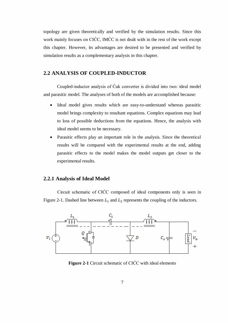
Circuit schematic of CIŠC composed of ideal components only is seen in
Figure 2-1. Dashed line between and represents the coupling of the inductors.
Figure 2-1 Circuit schematic of CIŠC with ideal elements
8
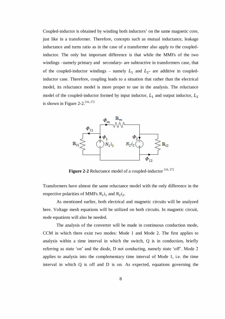
Coupled-inductor is obtained by winding both inductors‟ on the same magnetic core,
just like in a transformer. Therefore, concepts such as mutual inductance, leakage
inductance and turns ratio as in the case of a transformer also apply to the coupled-
inductor. The only but important difference is that while the MMFs of the two
windings –namely primary and secondary- are subtractive in transformers case, that
of the coupled-inductor windings – namely and - are additive in coupled-
inductor case. Therefore, coupling leads to a situation that rather than the electrical
model, its reluctance model is more proper to use in the analysis. The reluctance
model of the coupled-inductor formed by input inductor, and output inductor,
is shown in Figure 2-2.[16, 27]
Figure 2-2 Reluctance model of a coupled-inductor [16, 27]
Transformers have almost the same reluctance model with the only difference in the
respective polarities of MMFs and .
As mentioned earlier, both electrical and magnetic circuits will be analyzed
here. Voltage mesh equations will be utilized on both circuits. In magnetic circuit,
node equations will also be needed.
The analysis of the converter will be made in continuous conduction mode,
CCM in which there exist two modes: Mode 1 and Mode 2. The first applies to
analysis within a time interval in which the switch, Q is in conduction, briefly
referring as state „on‟ and the diode, D not conducting, namely state „off‟. Mode 2
applies to analysis into the complementary time interval of Mode 1, i.e. the time
interval in which Q is off and D is on. As expected, equations governing the
9
behaviour of the converter electrical circuit in both modes differ from each other.
Hence, electrical equations are grouped into two: Mode 1 and Mode 2. Unlike
electrical equations, however, magnetic equations are same for both modes.
2.2.1.1 Electrical Mesh Equations
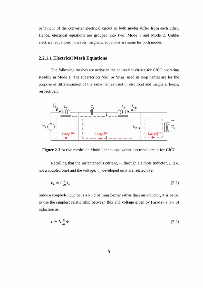
The following meshes are active in the equivalent circuit for CIŠC operating
steadily in Mode 1. The superscripts „elc‟ or „mag‟ used in loop names are for the
purpose of differentiation of the same names used in electrical and magnetic loops,
respectively.
Figure 2-3 Active meshes in Mode 1 in the equivalent electrical circuit for CIŠC
Recalling that the instantaneous current, through a simple inductor, (i.e.
not a coupled one) and the voltage, developed on it are related over
(2-1)
Since a coupled-inductor is a kind of transformer rather than an inductor, it is better
to use the simplest relationship between flux and voltage given by Faraday‟s law of
induction as;
(2-2)
10
Throughout the analyses, voltages of the windings are replaced by the help of this
law.
In Mode 1, (2-3)-(2-5) are the electrical mesh equations for the equivalent
circuit:
(2-3)
(2-4)
(2-5)
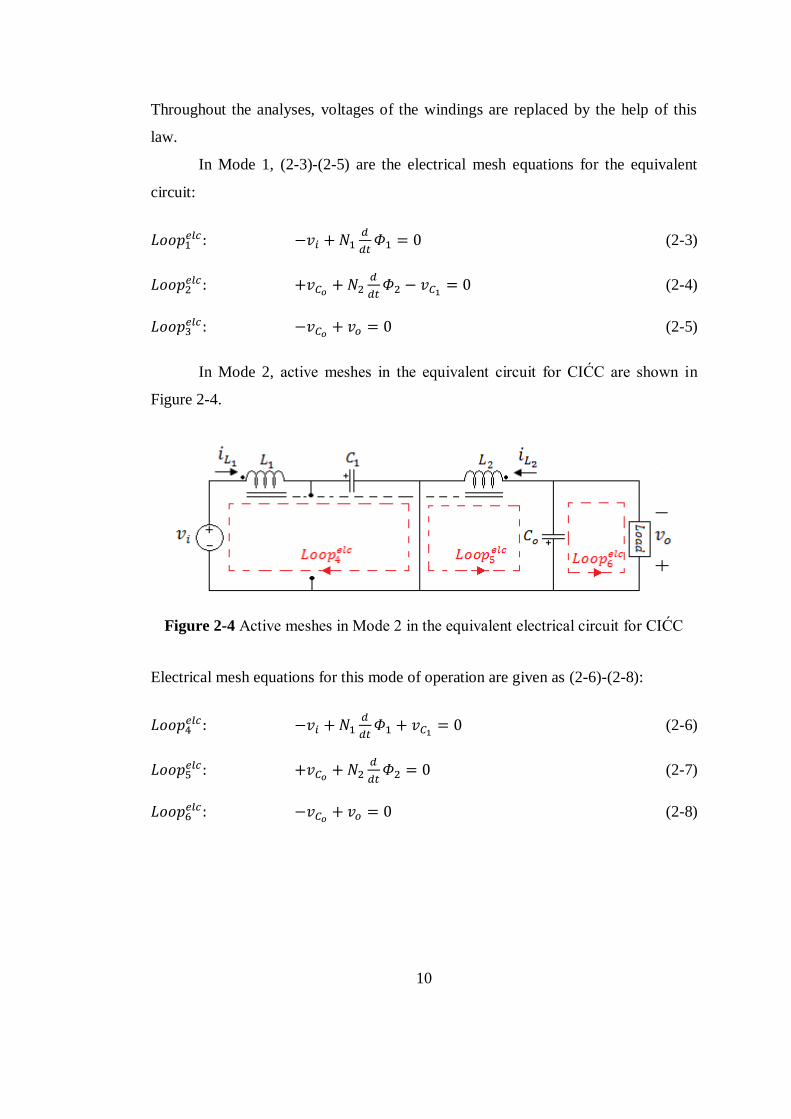
In Mode 2, active meshes in the equivalent circuit for CIŠC are shown in
Figure 2-4.
Figure 2-4 Active meshes in Mode 2 in the equivalent electrical circuit for CIŠC
Electrical mesh equations for this mode of operation are given as (2-6)-(2-8):
(2-6)
(2-7)
(2-8)
11
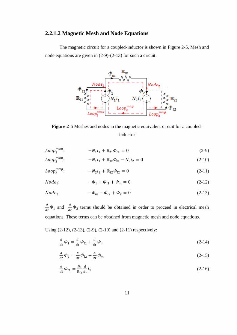
2.2.1.2 Magnetic Mesh and Node Equations
The magnetic circuit for a coupled-inductor is shown in Figure 2-5. Mesh and
node equations are given in (2-9)-(2-13) for such a circuit.
Figure 2-5 Meshes and nodes in the magnetic equivalent circuit for a coupled-
inductor
(2-9)
(2-10)
(2-11)
(2-12)
(2-13)
and
terms should be obtained in order to proceed in electrical mesh
equations. These terms can be obtained from magnetic mesh and node equations.
Using (2-12), (2-13), (2-9), (2-10) and (2-11) respectively:
(2-14)
(2-15)
(2-16)

12
(2-17)
(2-18)
Using (2-14), (2-16) and (2-17):
(2-19)
Using (2-15), (2-18) and (2-17):
(2-20)
2.2.1.3 Combination of Electrical and Magnetic Equations
Derivatives of the fluxes are obtained in terms of the derivatives of the
currents. Now, these results can be reflected to electrical mesh equations. As
mentioned earlier, magnetic equations are independent of the switch state. Hence (2-
19) and (2-20) are used for both electrical mesh equation sets.
In Mode 1, (2-21)-(2-23) are the magnetic mesh equations for the equivalent
circuit:
Using (2-3) and (2-19):
(2-21)
Using (2-4) and (2-20):
(2-22)
Using (2-5):
(2-23)
In Mode 2, (2-24)-(2-26) are the magnetic mesh equations for the equivalent
circuit:

13
Using (2-6) and (2-19):
(2-24)
Using (2-7) and (2-20):
(2-25)
Using (2-8):
(2-26)
Note that all the parameters are in terms of electrical quantities while taking into
account the magnetic connections and parameters.
In this work, state-space averaging method will be used in order to get
steady-state and dynamic model of the circuit. State variables are inductor currents
and capacitor voltages. Derivatives of capacitor voltages will be obtained in the next
chapter. For the derivatives of inductor currents, however, basic inductor equation
(2-1) cannot be used. Since a coupled-inductor is utilized, derivatives of inductor
currents should be obtained in terms of electrical quantities. Further simplification of
(2-21) and (2-22) in Mode 1 and (2-24) and (2-25) in Mode 2 gives the necessary and
ready-to-use information for the derivatives of the inductor currents. (2-23) and (2-
26) are written up to now just for mesh completeness and will not be used anymore.
Further simplification of (2-21) and (2-22) in Mode 1 gives:
(2-27)
(2-28)
where
(2-29)
(2-30)

14
(2-31)
(2-27) and (2-28) shows the representations of the derivatives of the inductor
currents in terms of the state-variables, namely and
, and the input variable,
namely , in Mode 1. Note that they do not include any flux-variable. When similar
simplification is applied to (2-24) and (2-25) in Mode 2, the following equations are
obtained:
(2-32)
(2-33)
At this point (2-27)-(2-28) and (2-32)-(2-33) are left as inputs to the next chapter.
This chapter continues with the merits of using coupled-inductor in basic Šuk
converter.
2.2.2 Merits of Coupling
In this section, by the help of some reasonable assumptions, merits of
coupling will be proven theoretically. Those merits are either ripple-free input
current waveform or ripple-free output current waveform. (2-21)-(2-22) and (2-24)-
(2-25) are the input equations to this section. Then, some simplifications and
assumptions are needed in order to proceed. These assumptions are either mentioned
explicitly or implied in [8, 16, 26].
Assumption 2-1: Input voltage is constant.
(2-34)
Assumption 2-2: Voltage on the output capacitor, is almost constant i.e. its
voltage ripple is negligible.
(2-35)

15
Simplification 2-1: Mean value of the voltage on , is the sum of the mean
value of the input voltage, and the mean value of the output voltage, .[2
] This
fact, which is obtained in CHAPTER 3, is also explained below in another way.
When the outermost loop voltage equation –starting with in the clockwise
direction- is written, the following equation is obtained.
(2-36)
As known, the mean values of the inductors‟ voltages are zero at steady-state.
(2-37)
(2-38)
Therefore, taking the mean values of both sides of the equation gives that:
(2-39)
Negligible ripple assumption permits this simplification be utilized in the electrical
mesh equations.
Assumption 2-3: Voltage on capacitor, is almost constant i.e. its voltage ripple
is negligible.
(2-40)
As a result of these assumptions and the simplification, the following
equation sets are obtained.
In Mode 1:
Using (2-21) and (2-34):
(2-41)

16
Using (2-22), (2-39), (2-34) and (2-35):
(2-42)
In Mode 2:
Using (2-24), (2-39), (2-34) and (2-35):
(2-43)
Using (2-25) and (2-35):
(2-44)
Following two sections present the conditions for ripple-free current either at
input or output and also the simulation results that verify the theoretical analyses.
2.2.2.1 Ripple-Free Input Current
The requirement is to obtain ripple-free input current. Input current is the
same as the current of , or simply .
(2-45)
Since it is constant, its derivative is zero.
(2-46)
When this condition is applied to (2-41)-(2-44), some restrictions arises. If those
restrictions turn out to be applicable, it means that zero-ripple input current
waveform is possible to obtain. Moreover, the restrictions should be applicable for
both modes.

17
In Mode 1:
Using (2-41) and (2-46):
(2-47)
Using (2-42) and (2-46):
(2-48)
In Mode 2:
Using (2-43) and (2-46):
(2-49)
Using (2-44) and (2-46):
(2-50)
For the input current to be ripple-free in Mode 1, the following condition has
to be satisfied.
Using (2-47) and (2-48):
(2-51)
The same condition is also required for the input current to be ripple-free in Mode 2.
Using (2-49) and (2-50):
(2-52)
Since the same condition makes the input current ripple-free in both modes, namely
the entire period, it can be proven that applying this condition satisfies to obtain a
ripple-free input current. (2-52) can be simplified into the following form.

18
(2-53)
Since is much larger than , equivalent reluctance of turns out to be
a little bit smaller than . Hence, (2-53) dictates that has to be a little bit larger
than , which seems to be reasonable and applicable.
Simply equating (2-47) to (2-48) and (2-49) to (2-50) gives the requirement
for ripple-free input current mathematically. How can it be possible? What is its
physical interpretation? There is a condition here. Actually, the left hand sides of
these four equations represent the voltage applied to the windings. is applied to
inductors in Mode 1 and in Mode 2. That is, inductors have the same voltage
waveforms. It is this result which leads to an applicable condition on turns ratio and
reluctances. Otherwise, the resultant condition would turn out to be meaningless and
not applicable, which would imply that ripple-free input current is not possible.
When it is worked on, it is seen that the exact condition on coupling the
inductors is a little bit different: Inductors have to have proportional waveforms
rather than equal.[8
, 10, 13] Although it was first suggested by Šuk, coupled-inductor
is not specific to Šuk converter only. It can be used in output filter inductors of
multiple output converters, as well. There, voltage waveforms of output inductors are
not generally equal but proportional. Since only Šuk converter is considered in this
work and it has equal voltage waveforms on its coupled-inductors, proportional
voltage waveform condition will not be proven here.
Now, ripple-free input current analysis will be proven by simulation. Ansoft
Simplorer simulation program will be used for this purpose. It presents the facility of
designing any magnetic element and establishing any magnetic circuitry. In that
program, coupled-inductor can be implemented in two ways. It only differs
according to the implementation of the leakage inductances.
In Figure 2-6, first possible CIŠC implementation in Simplorer is shown. It is
a snapshot of the circuit implementation in the simulation program. Only the labels
are modified in order to provide label consistency. Orange lines represent magnetic
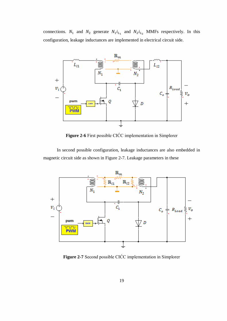
19
connections. and generate and
MMFs respectively. In this
configuration, leakage inductances are implemented in electrical circuit side.
Figure 2-6 First possible CIŠC implementation in Simplorer
In second possible configuration, leakage inductances are also embedded in
magnetic circuit side as shown in Figure 2-7. Leakage parameters in these
Figure 2-7 Second possible CIŠC implementation in Simplorer

20
configurations are related to each other as dictated by (2-63) and (2-64). Both
configurations give the same waveform results.
Simulation is conducted at the following operating point.
Simulation is performed with the ideal electrical components. In other words;
the switch, the diode and the capacitors are assumed to be ideal. and are the
ones that have been selected in the design chapter in terms of capacitance values.
: Ideal switch : Ideal diode
: Ideal capacitor, 3000uF : Ideal capacitor, 23.5uF
As a magnetic element, the following values are used. These values belong to
the designed coupled-inductor in the design chapter. Detailed information is
presented there.
Above values give the following parameters.
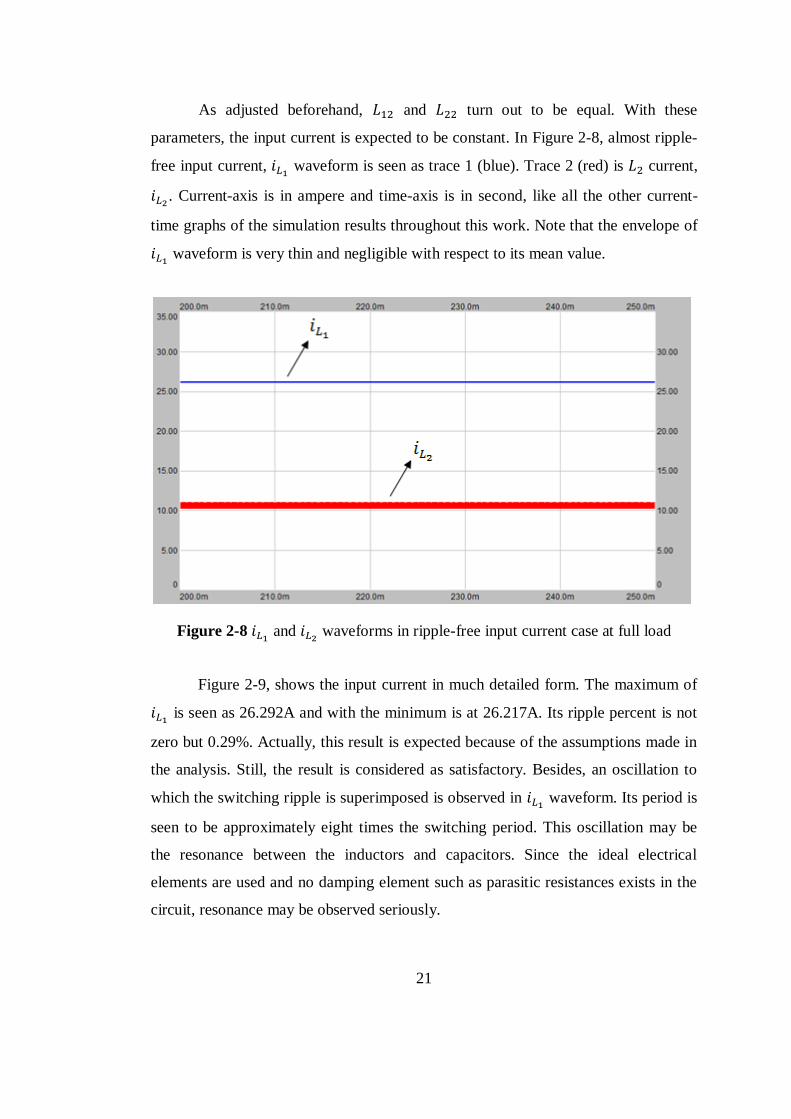
21
As adjusted beforehand, and turn out to be equal. With these
parameters, the input current is expected to be constant. In Figure 2-8, almost ripple-
free input current, waveform is seen as trace 1 (blue). Trace 2 (red) is current,
. Current-axis is in ampere and time-axis is in second, like all the other current-
time graphs of the simulation results throughout this work. Note that the envelope of
waveform is very thin and negligible with respect to its mean value.
Figure 2-8 and
waveforms in ripple-free input current case at full load
Figure 2-9, shows the input current in much detailed form. The maximum of
is seen as 26.292A and with the minimum is at 26.217A. Its ripple percent is not
zero but 0.29%. Actually, this result is expected because of the assumptions made in
the analysis. Still, the result is considered as satisfactory. Besides, an oscillation to
which the switching ripple is superimposed is observed in waveform. Its period is
seen to be approximately eight times the switching period. This oscillation may be
the resonance between the inductors and capacitors. Since the ideal electrical
elements are used and no damping element such as parasitic resistances exists in the
circuit, resonance may be observed seriously.
22
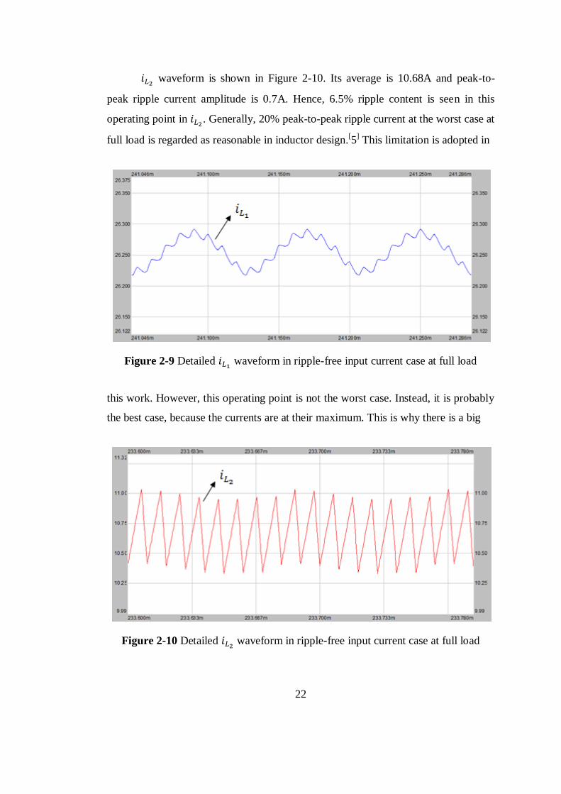
waveform is shown in Figure 2-10. Its average is 10.68A and peak-to-
peak ripple current amplitude is 0.7A. Hence, 6.5% ripple content is seen in this
operating point in . Generally, 20% peak-to-peak ripple current at the worst case at
full load is regarded as reasonable in inductor design.[5
] This limitation is adopted in
Figure 2-9 Detailed waveform in ripple-free input current case at full load
this work. However, this operating point is not the worst case. Instead, it is probably
the best case, because the currents are at their maximum. This is why there is a big
Figure 2-10 Detailed waveform in ripple-free input current case at full load
23
gap between 6.5% and 20%, and small gap between 6.5% and 0.29%. Besides, note
that the same oscillation is observed in waveform.
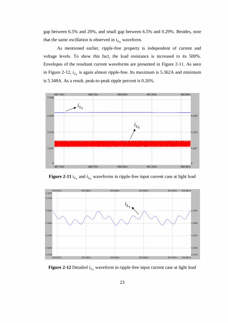
As mentioned earlier, ripple-free property is independent of current and
voltage levels. To show this fact, the load resistance is increased to its 500%.
Envelopes of the resultant current waveforms are presented in Figure 2-11. As seen
in Figure 2-12, is again almost ripple-free. Its maximum is 5.362A and minimum
is 5.348A. As a result, peak-to-peak ripple percent is 0.26%.
Figure 2-11 and
waveforms in ripple-free input current case at light load
Figure 2-12 Detailed waveform in ripple-free input current case at light load
24
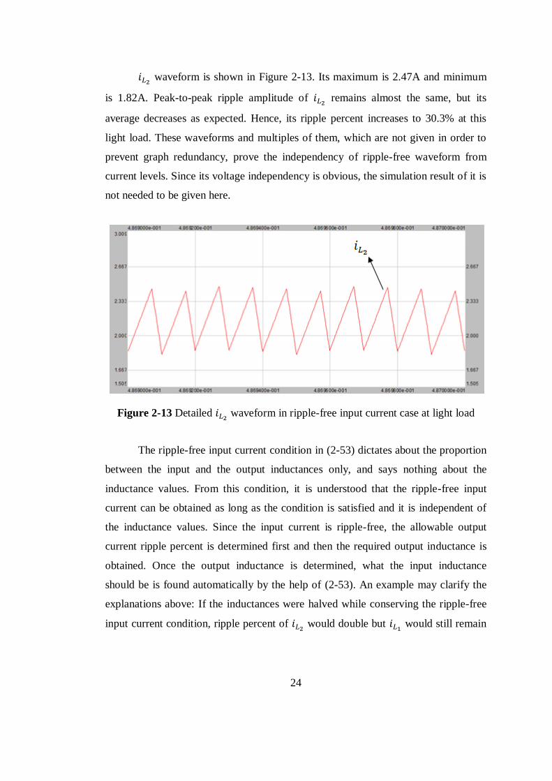
waveform is shown in Figure 2-13. Its maximum is 2.47A and minimum
is 1.82A. Peak-to-peak ripple amplitude of remains almost the same, but its
average decreases as expected. Hence, its ripple percent increases to 30.3% at this
light load. These waveforms and multiples of them, which are not given in order to
prevent graph redundancy, prove the independency of ripple-free waveform from
current levels. Since its voltage independency is obvious, the simulation result of it is
not needed to be given here.
Figure 2-13 Detailed waveform in ripple-free input current case at light load
The ripple-free input current condition in (2-53) dictates about the proportion
between the input and the output inductances only, and says nothing about the
inductance values. From this condition, it is understood that the ripple-free input
current can be obtained as long as the condition is satisfied and it is independent of
the inductance values. Since the input current is ripple-free, the allowable output
current ripple percent is determined first and then the required output inductance is
obtained. Once the output inductance is determined, what the input inductance
should be is found automatically by the help of (2-53). An example may clarify the
explanations above: If the inductances were halved while conserving the ripple-free
input current condition, ripple percent of would double but
would still remain

25
as ripple-free. This fact is also observed in simulation but the result is not given here.
This argument is also valid for the ripple-free output current case.
Another argument is about decoupling of the inductors. If inductors were
decoupled without changing their inductances, would show the same waveform
and would have a waveform and ripple content similar to
. Further information
on this issue can be found in [8, 10].
2.2.2.2 Ripple-Free Output Current
This time the requirement is to obtain a ripple-free output current. The output
current is not the same as because of the intervention of output capacitor current.
However, constant output current requirement brings the fact that output capacitor
current is always zero. Hence, is equal to the output current for this requirement.
(2-54)
In this case, current is defined as a constant.
(2-55)
The same procedure is applied for ripple-free output current case. At the end, the
following condition is obtained for a ripple-free output current waveform.
Using (2-41)-(2-44) and (2-55):
(2-56)
Further simplification gives that:
(2-57)

26
Similarly, since is much larger than , equivalent reluctance of turns
out to be a little bit smaller than . Hence, (2-57) dictates that has to be a little
bit larger than . As a result, remembering the ripple-free input current case, the
side which is desired to have ripple-free current waveform should have a little bit
larger number of turns.
The requirement for coupling the inductors –namely proportional voltage
waveforms on inductors- also applies here.
Now, ripple-free output current waveform will be verified by simulation. For
this purpose, there is no need to design a new coupled-inductor. Just toggling and
in ripple-free input current case is enough. That is, the same parameters will be
used, but - and - values will be interchanged.
These parameters give that:
In this situation, is satisfied and output current is expected to be ripple-
free. As seen in Figure 2-14, Figure 2-15 and Figure 2-16; is almost ripple-free
and has considerable ripple content as expected. In these figures, again trace 1
(blue) represents and trace 2 (red)
. Envelopes of the current waveforms are
shown in Figure 2-14. Envelope of is very thin, which means that its ripple
content is very low.
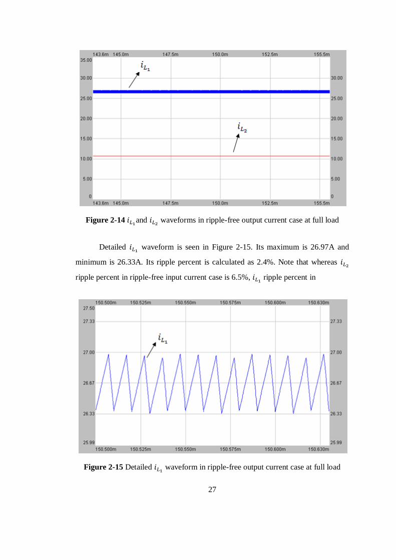
27
Figure 2-14 and
waveforms in ripple-free output current case at full load
Detailed waveform is seen in Figure 2-15. Its maximum is 26.97A and
minimum is 26.33A. Its ripple percent is calculated as 2.4%. Note that whereas
ripple percent in ripple-free input current case is 6.5%, ripple percent in
Figure 2-15 Detailed waveform in ripple-free output current case at full load
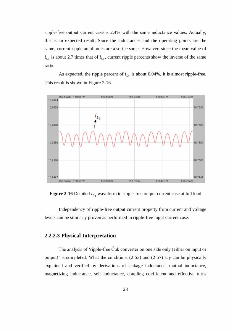
28
ripple-free output current case is 2.4% with the same inductance values. Actually,
this is an expected result. Since the inductances and the operating points are the
same, current ripple amplitudes are also the same. However, since the mean value of
is about 2.7 times that of
, current ripple percents show the inverse of the same
ratio.
As expected, the ripple percent of is about 0.04%. It is almost ripple-free.
This result is shown in Figure 2-16.
Figure 2-16 Detailed waveform in ripple-free output current case at full load
Independency of ripple-free output current property from current and voltage
levels can be similarly proven as performed in ripple-free input current case.
2.2.2.3 Physical Interpretation
The analysis of „ripple-free Šuk converter on one side only (either on input or
output)‟ is completed. What the conditions (2-53) and (2-57) say can be physically
explained and verified by derivations of leakage inductance, mutual inductance,
magnetizing inductance, self inductance, coupling coefficient and effective turns
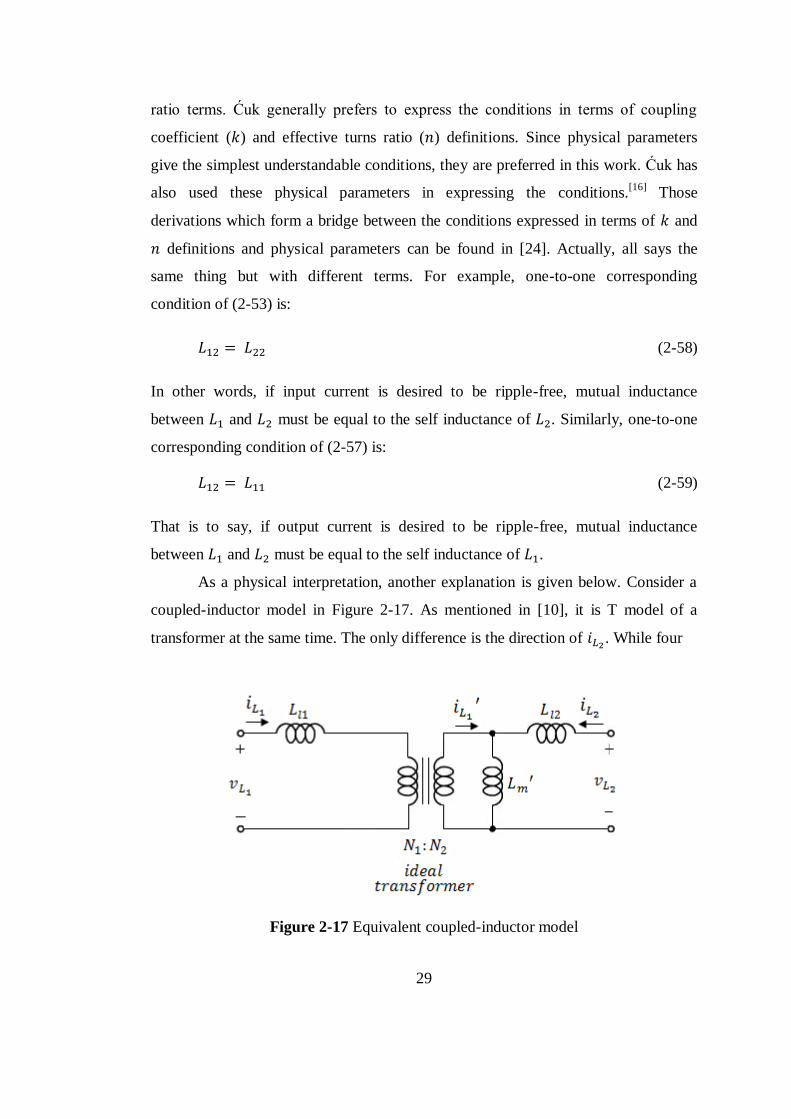
29
ratio terms. Šuk generally prefers to express the conditions in terms of coupling
coefficient ( ) and effective turns ratio ( ) definitions. Since physical parameters
give the simplest understandable conditions, they are preferred in this work. Šuk has
also used these physical parameters in expressing the conditions.[16]
Those
derivations which form a bridge between the conditions expressed in terms of and
definitions and physical parameters can be found in [24]. Actually, all says the
same thing but with different terms. For example, one-to-one corresponding
condition of (2-53) is:
(2-58)
In other words, if input current is desired to be ripple-free, mutual inductance
between and must be equal to the self inductance of . Similarly, one-to-one
corresponding condition of (2-57) is:
(2-59)
That is to say, if output current is desired to be ripple-free, mutual inductance
between and must be equal to the self inductance of .
As a physical interpretation, another explanation is given below. Consider a
coupled-inductor model in Figure 2-17. As mentioned in [10], it is T model of a
transformer at the same time. The only difference is the direction of . While four
Figure 2-17 Equivalent coupled-inductor model

30
electrical variables (
) are all positive or negative with respect to the
model in coupled-inductor operation, the polarity of is the inverse of the other
three variables in transformer operation with respect to the model in Figure 2-17.
The derivations of the following basic relationships can be found in [24].
(2-60)
(2-61)
(2-62)
(2-63)
(2-64)
(2-65)
(2-66)
By using these basic relationships, ripple-free current conditions can be obtained.
Let‟s consider the ripple-free input current case. For to be ripple-free, voltage on
should always be zero, otherwise current –hence - would change. How can
it be possible? If voltage applied to the negative terminal of is always equal to the
voltage applied to the positive terminal of , its current remains at the same level. It
is known that is equal to
. Let it be . Although they have two different values
in a period, they are always equal in time.
(2-67)
Then, by voltage division rule, voltage on is calculated as in (2-68). At first look
it seems that
current interferes with
, hence voltage division cannot be applied.
However, this voltage division is due to the derivative of the current term rather than

31
the current itself. Since
is constant, voltage division can be applicable. That is,
there is no voltage induced on due to
.
(2-68)
Since the same flux links the both windings, voltages induced on and are
proportional to their number of turns.
(2-69)
Using (2-69), (2-62) and (2-66):
(2-70)
As stated in (2-58), is adjusted to be equal to for ripple-free input current
case. That condition leads to the following simplification.
(2-71)
Voltage applied to the negative terminal of is found to be . Since the voltage
applied to the positive terminal of is also , current remains constant. Note
that it is valid as long as the voltages applied to both windings are the same and
independent of the voltage or current levels. Similarly, the same procedure can be
applied to the ripple-free output current case and the same results can be obtained.
2.2.3 Analysis of Parasitic Model
Circuit schematic of coupled-inductor Šuk converter composed of ideal
components together with their well-known parasitic elements is shown in Figure
2-18. Derivation of this model can be found in [2]. and
represent the ESRs
of the corresponding capacitances. and
are the resistances of the
corresponding inductors. is the on-state resistance of the switch, which is a

32
MOSFET. is the forward voltage drop and is the forward resistance of the
diode. As understood from the capital letters, parasitic elements are assumed to be
constant.
Figure 2-18 Circuit schematic of CIŠC with ideal components together with their
well-known parasitic elements
The procedure that was applied to CIŠC with ideal components will be
applied to this model. In order not to cause repetition, some steps are omitted.
2.2.3.1 Electrical Mesh Equations
This time, and
in Figure 2-3 are written for the parasitic
model.
In Mode 1:
(2-72)
(2-73)
In Mode 2:
(2-74)

33
(2-75)
2.2.3.2 Magnetic Mesh and Node Equations
Magnetic circuit already includes the parasitic elements, namely the
reluctances. Hence, (2-19) and (2-20) will directly be utilized for this analysis.
2.2.3.3 Combination of Electrical and Magnetic Equations
In Mode 1, the following equation set is obtained.
In Mode 1:
Using (2-72) and (2-19):
(2-76)
Using (2-73) and (2-20):
(2-77)
Similarly, in Mode 2, the following equation set is obtained.
In Mode 2:
Using (2-74) and (2-19):
(2-78)

34
Using (2-75) and (2-20):
(2-79)
Using (2-76)-(2-79), derivatives of the two state-variables –namely and
- can
be written in terms of state-variables and input variables. Before that, some
simplification should be done as an addition to (2-29)-(2-31).
In Mode 1:
Using (2-76) and (2-77):
(2-80)
(2-81)
In Mode 2:
Using (2-78) and (2-79):
(2-82)
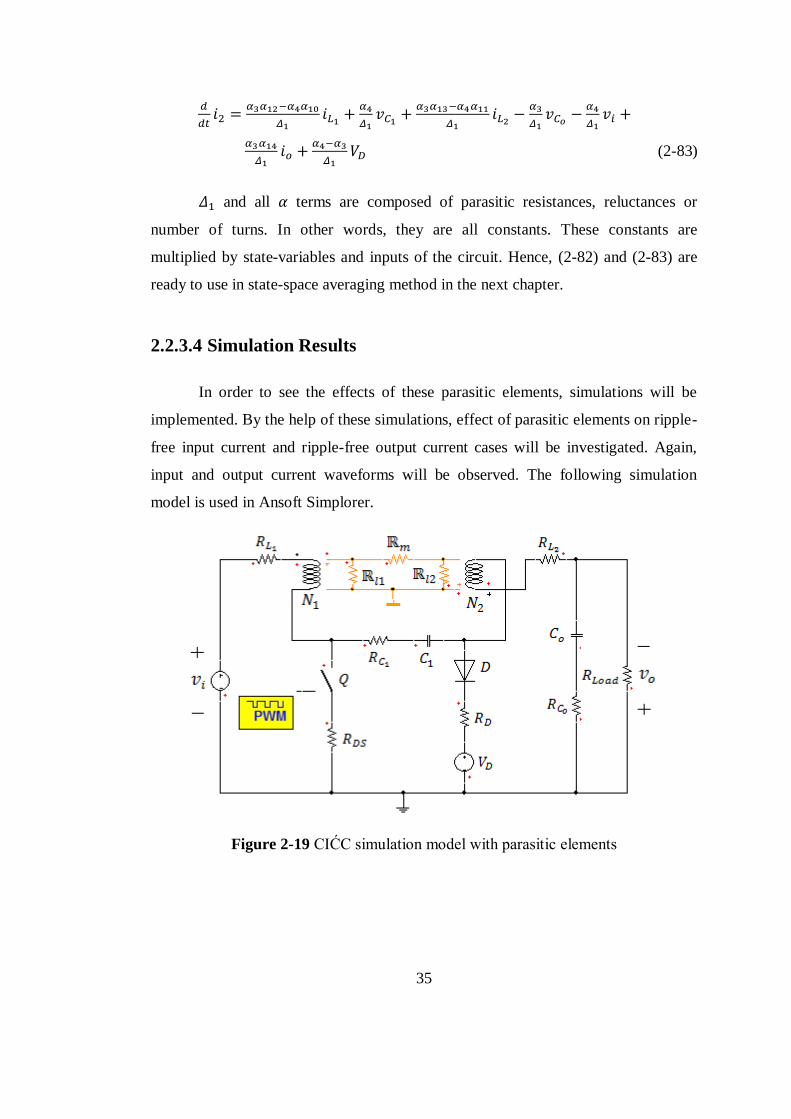
35
(2-83)
and all terms are composed of parasitic resistances, reluctances or
number of turns. In other words, they are all constants. These constants are
multiplied by state-variables and inputs of the circuit. Hence, (2-82) and (2-83) are
ready to use in state-space averaging method in the next chapter.
2.2.3.4 Simulation Results
In order to see the effects of these parasitic elements, simulations will be
implemented. By the help of these simulations, effect of parasitic elements on ripple-
free input current and ripple-free output current cases will be investigated. Again,
input and output current waveforms will be observed. The following simulation
model is used in Ansoft Simplorer.
Figure 2-19 CIŠC simulation model with parasitic elements
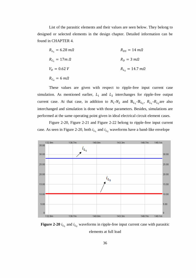
36
List of the parasitic elements and their values are seen below. They belong to
designed or selected elements in the design chapter. Detailed information can be
found in CHAPTER 4.
These values are given with respect to ripple-free input current case
simulation. As mentioned earlier, and interchanges for ripple-free output
current case. At that case, in addition to - and -
, -
are also
interchanged and simulation is done with those parameters. Besides, simulations are
performed at the same operating point given in ideal electrical circuit element cases.
Figure 2-20, Figure 2-21 and Figure 2-22 belong to ripple-free input current
case. As seen in Figure 2-20, both and
waveforms have a band-like envelope
Figure 2-20 and
waveforms in ripple-free input current case with parasitic
elements at full load
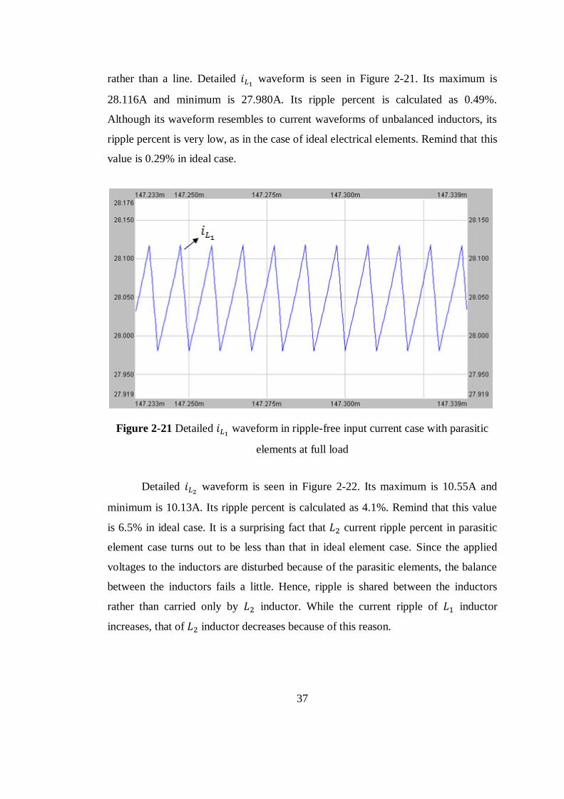
37
rather than a line. Detailed waveform is seen in Figure 2-21. Its maximum is
28.116A and minimum is 27.980A. Its ripple percent is calculated as 0.49%.
Although its waveform resembles to current waveforms of unbalanced inductors, its
ripple percent is very low, as in the case of ideal electrical elements. Remind that this
value is 0.29% in ideal case.
Figure 2-21 Detailed waveform in ripple-free input current case with parasitic
elements at full load
Detailed waveform is seen in Figure 2-22. Its maximum is 10.55A and
minimum is 10.13A. Its ripple percent is calculated as 4.1%. Remind that this value
is 6.5% in ideal case. It is a surprising fact that current ripple percent in parasitic
element case turns out to be less than that in ideal element case. Since the applied
voltages to the inductors are disturbed because of the parasitic elements, the balance
between the inductors fails a little. Hence, ripple is shared between the inductors
rather than carried only by inductor. While the current ripple of inductor
increases, that of inductor decreases because of this reason.
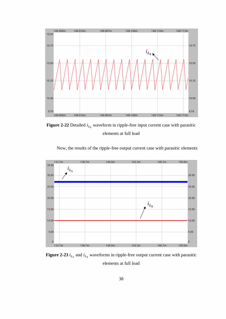
38
Figure 2-22 Detailed waveform in ripple-free input current case with parasitic
elements at full load
Now, the results of the ripple-free output current case with parasitic elements
Figure 2-23 and
waveforms in ripple-free output current case with parasitic
elements at full load
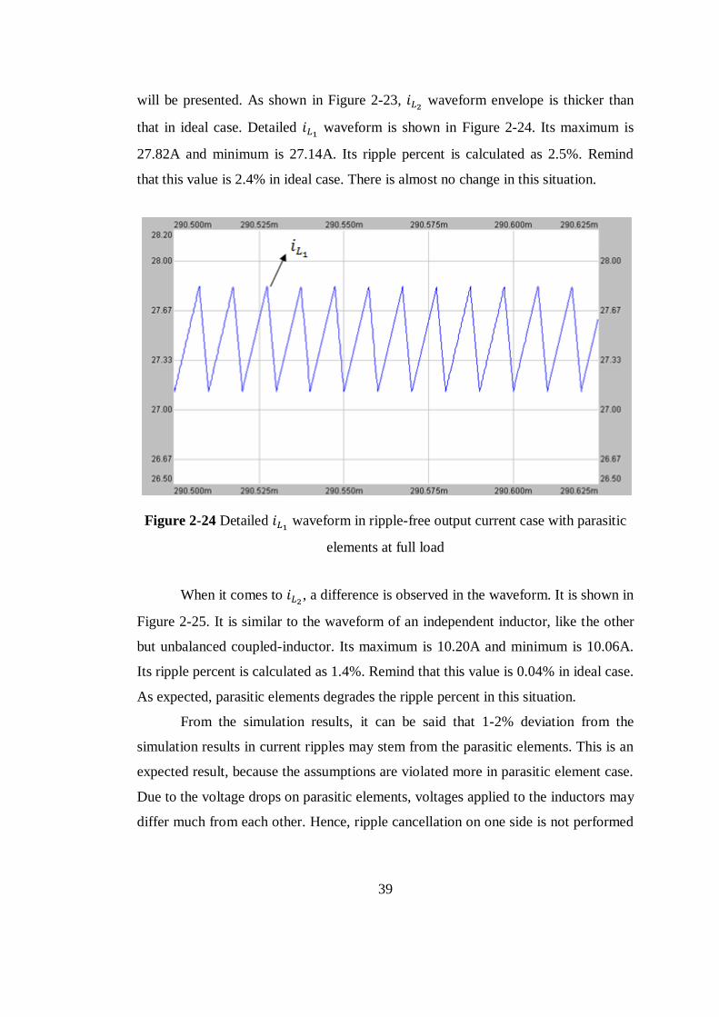
39
will be presented. As shown in Figure 2-23, waveform envelope is thicker than
that in ideal case. Detailed waveform is shown in Figure 2-24. Its maximum is
27.82A and minimum is 27.14A. Its ripple percent is calculated as 2.5%. Remind
that this value is 2.4% in ideal case. There is almost no change in this situation.
Figure 2-24 Detailed waveform in ripple-free output current case with parasitic
elements at full load
When it comes to , a difference is observed in the waveform. It is shown in
Figure 2-25. It is similar to the waveform of an independent inductor, like the other
but unbalanced coupled-inductor. Its maximum is 10.20A and minimum is 10.06A.
Its ripple percent is calculated as 1.4%. Remind that this value is 0.04% in ideal case.
As expected, parasitic elements degrades the ripple percent in this situation.
From the simulation results, it can be said that 1-2% deviation from the
simulation results in current ripples may stem from the parasitic elements. This is an
expected result, because the assumptions are violated more in parasitic element case.
Due to the voltage drops on parasitic elements, voltages applied to the inductors may
differ much from each other. Hence, ripple cancellation on one side is not performed
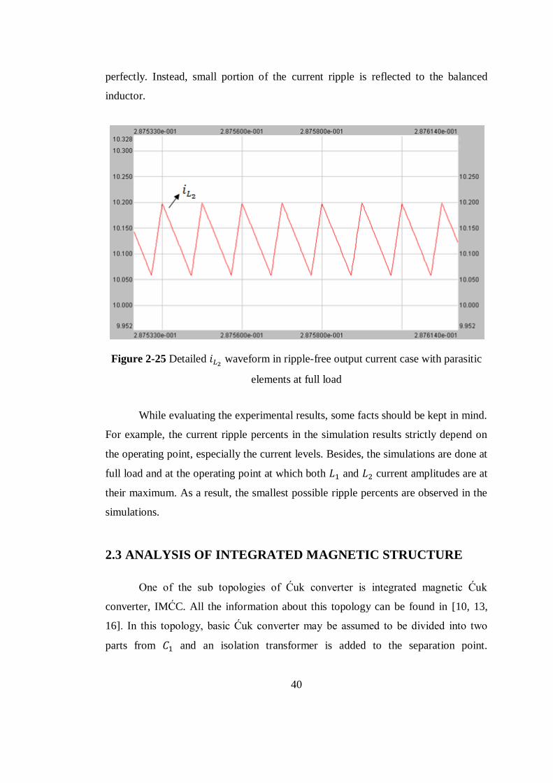
40
perfectly. Instead, small portion of the current ripple is reflected to the balanced
inductor.
Figure 2-25 Detailed waveform in ripple-free output current case with parasitic
elements at full load
While evaluating the experimental results, some facts should be kept in mind.
For example, the current ripple percents in the simulation results strictly depend on
the operating point, especially the current levels. Besides, the simulations are done at
full load and at the operating point at which both and current amplitudes are at
their maximum. As a result, the smallest possible ripple percents are observed in the
simulations.
2.3 ANALYSIS OF INTEGRATED MAGNETIC STRUCTURE
One of the sub topologies of Šuk converter is integrated magnetic Šuk
converter, IMŠC. All the information about this topology can be found in [10, 13,
16]. In this topology, basic Šuk converter may be assumed to be divided into two
parts from and an isolation transformer is added to the separation point.

41
Therefore, output is galvanically isolated from input. „Integrated magnetic‟ name is
fitted to this topology because not only the input and output inductors but also the
transformer share the same magnetic core. Transformer‟s primary and secondary
windings together with the input and output inductors are wound on the same core.
Hence, this component is called integrated magnetic structure.
IMŠC brings another advantage together with isolation. By the presence of
integrated magnetic structure, it is possible to obtain ripple-free input and output
waveforms at the same time. As expected, this is possible as long as some conditions
are satisfied in design of the integrated magnetic structure. Also, as in case of CIŠC,
this property is independent of the operating condition. When all the properties of
IMŠC are considered, it is possible to say that this topology simulates a dc-to-dc
transformer with variable turns ratio.[10, 12]
Because
it is isolated,
it has totally dc input/output voltage/current waveforms,
and its turns ratio can be adjusted with duty-factor.
Inspired by the integrated magnetic structure models proposed in [16],
complete reluctance model of integrated magnetic structure is proposed in this
section. Its analysis will be done and then verified by the simulations. Analysis will
be done with ideal electrical circuit components. Its parasitical model is left for
further studies. At the end of the analysis, it is intended to obtain the conditions for
ripple-free input and output waveforms at the same time. Contrary to the case of
coupled-inductor, obtaining the derivatives of the two state-variables –namely
and - in terms of other state-variables and input variables is not aimed here. It is
again left for further studies. Therefore, and
are replaced by the requirement –
that is, they are constants- whenever they are faced with throughout the analysis for
simplicity.
2.3.1 Analysis of Ideal Model and Merits of Coupling
The circuit schematic of IMŠC is seen in Figure 2-26.
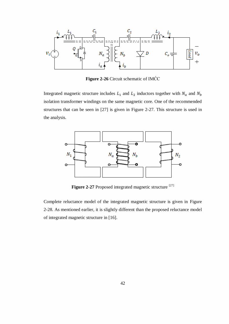
42
Figure 2-26 Circuit schematic of IMŠC
Integrated magnetic structure includes and inductors together with and
isolation transformer windings on the same magnetic core. One of the recommended
structures that can be seen in [27] is given in Figure 2-27. This structure is used in
the analysis.
Figure 2-27 Proposed integrated magnetic structure [27]
Complete reluctance model of the integrated magnetic structure is given in Figure
2-28. As mentioned earlier, it is slightly different than the proposed reluctance model
of integrated magnetic structure in [16].
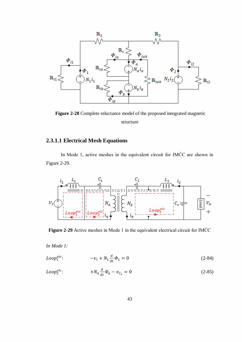
43
Figure 2-28 Complete reluctance model of the proposed integrated magnetic
structure
2.3.1.1 Electrical Mesh Equations
In Mode 1, active meshes in the equivalent circuit for IMŠC are shown in
Figure 2-29.
Figure 2-29 Active meshes in Mode 1 in the equivalent electrical circuit for IMŠC
In Mode 1:
:
(2-84)
:
(2-85)
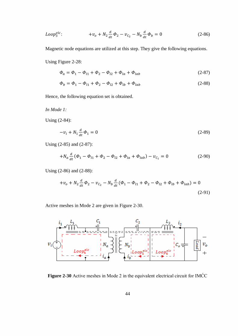
44
:
(2-86)
Magnetic node equations are utilized at this step. They give the following equations.
Using Figure 2-28:
(2-87)
(2-88)
Hence, the following equation set is obtained.
In Mode 1:
Using (2-84):
(2-89)
Using (2-85) and (2-87):
(2-90)
Using (2-86) and (2-88):
(2-91)
Active meshes in Mode 2 are given in Figure 2-30.
Figure 2-30 Active meshes in Mode 2 in the equivalent electrical circuit for IMŠC

45
In Mode 2:
:
(2-92)
:
(2-93)
:
(2-94)
By the replacement of and , the following equation set is obtained.
In Mode 2:
Using (2-92) and (2-87):
(2-95)
Using (2-93) and (2-88):
(2-96)
Using (2-94):
(2-97)
Assumptions utilized in the coupled-inductor analysis are also used here.
However, there are some differences stemming from the isolation transformer. (2-39)
were valid in the previous analysis. In this analysis, however, the followings are
valid.
(2-98)
(2-99)
When these simplifications together with the previous assumptions made in coupled-
inductor analysis are applied, the following equation set is obtained.

46
In Mode 1:
Using (2-89) and (2-34):
(2-100)
Using (2-90), (2-40) and (2-98):
(2-101)
Using (2-91), (2-35), (2-40) and (2-99):
(2-102)
In Mode 2:
Using (2-95), (2-34), (2-40) and (2-98):
(2-103)
Using (2-96), (2-40) and (2-99):
(2-104)
Using (2-97) and (2-35):
(2-105)
2.3.1.2 Magnetic Mesh Equations
Using the following magnetic circuit, mesh equations can be obtained.

47
Figure 2-31 Active meshes in magnetic circuit schematic of integrated magnetic
structure
Two Major Loops:
:
(2-106)
:
(2-107)
Five Minor Loops:
: (2-108)
: (2-109)
: (2-110)
: (2-111)
: (2-112)

48
,
,
,
,
,
and
terms should be obtained
in order to proceed in electrical mesh equations. These terms can be obtained from
magnetic mesh equations.
In this configuration, it is claimed that both input and output current can be
made ripple-free. Hence, derivatives of input and output current can be equated to
zero.
(2-113)
Note: By using (2-113) or the assumptions such as constant capacitor voltages that
will be used later, the chance of obtaining
and
in terms of state-variables
and input variables is lost intentionally. If state-space averaging method were to be
applied to IMŠC in this work,
and
terms would be easily prepared as inputs
to that method. However, only the conditions for ripple-free input and output current
are intended to give in this section.
By taking the derivative of the magnetic loop equations and using (2-113),
the following equation set is obtained.
Five Minor Loops:
Using (2-108)-(2-112) and (2-113):
(2-114)
(2-115)
(2-116)
(2-117)
(2-118)

49
Two Major Loops:
Using (2-106), (2-113)-(2-115):
(2-119)
Using (2-107), (2-113)-(2-115):
(2-120)
and
terms are expressed in terms of
and
, which are electrical parameters. Now,
and
terms should be
expressed in the same manner. Using (2-119) and (2-120), they can be obtained
easily.
:
(2-121)
:
(2-122)
For further simplification, Mode 1 and Mode 2 can be considered separately for
magnetic loop equations. From Figure 2-29 it is clearly seen that during in
Mode 1.
In Mode 1:
(2-123)
Similarly, is equal to in Mode 2. This fact can be seen in Figure 2-30.
In Mode 2:
(2-124)
Magnetic equations can now be separately written for Mode 1 and Mode 2.
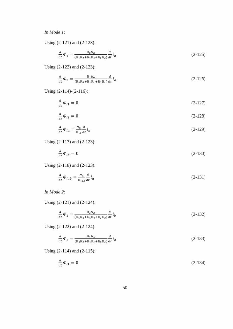
50
In Mode 1:
Using (2-121) and (2-123):
(2-125)
Using (2-122) and (2-123):
(2-126)
Using (2-114)-(2-116):
(2-127)
(2-128)
(2-129)
Using (2-117) and (2-123):
(2-130)
Using (2-118) and (2-123):
(2-131)
In Mode 2:
Using (2-121) and (2-124):
(2-132)
Using (2-122) and (2-124):
(2-133)
Using (2-114) and (2-115):
(2-134)

51
(2-135)
Using (2-116) and (2-124):
(2-136)
Using (2-117):
(2-137)
Using (2-118) and (2-124):
(2-138)
Derivatives of the fluxes are obtained in terms of the derivates of the currents. Now,
these results can be reflected to electrical mesh equations. Before that, the following
notation simplification can be useful.
(2-139)
In Mode 1:
Using (2-84), (2-125) and (2-139):
(2-140)
Using (2-101), (2-125)-(2-129), (2-131) and (2-139):
(2-141)
Using (2-102), (2-125)-(2-128), (2-130)-(2-131) and (2-139):
(2-142)
(2-142) implies that will be greater than , which is possible.

52
In Mode 2:
Using (2-103), (2-132)-(2-136) and (2-138)-(2-139):
(2-143)
(2-143) implies that will be greater than , which is also possible.
Using (2-104), (2-132)-(2-135) and (2-137)-(2-139):
(2-144)
Using (2-105), (2-133) and (2-139):
(2-145)
When analyzed, it can be seen that all four windings have the same voltage
waveform: in Mode 1 and during in Mode 2. This fact also appears in the
equation set above. As mentioned earlier, in coupled-inductor analysis, windings
have to have proportional voltage waveforms. That condition is also valid here. The
same arguments in coupled-inductor case can be applied to this equation set.
Further simplification may give simple conditions for ripple-free current
waveforms on both sides.
Using (2-140) and (2-141):
(2-146)
Using (2-143) and (2-146):
(2-147)
Since and are intentionally put and just represents the leakage, (2-147)
means that has to tend to infinity in order to satisfy this equality. Of course, this
is not a practical result. However, is expected to be very high because it
represents only the leakage of the primary winding. Even its part of the mutual flux

53
with secondary winding which does not couple any of the inductor is not included in
this term. For example, twisting the primary and secondary windings of the
transformer can make very high. Hence, this condition can be accepted as
reasonable.
Using (2-144) and (2-145):
(2-148)
Using (2-142) and (2-148):
(2-149)
The same argument is also valid for . As a result, the following four conditions
have to be satisfied for ripple-free input and output current waveforms
simultaneously.
2.3.1.3 Conditions for Zero-Ripple at Both Ends Simultaneously
In this section, conditions for ripple-free input and output current waveforms
simultaneously are gathered together as (2-150)-(2-153).
Using (2-143), (2-147), (2-142), (2-149) respectively:
(2-150)
(2-151)
(2-152)
(2-153)
Although the conditions above seem to be highly different than the coupled-
inductor case, they resembles to the results obtained in that analysis much. What the
conditions (2-150)-(2-153) say can be physically explained and verified by the

54
derivations of leakage inductance, mutual inductance, magnetizing inductance, self
inductance, coupling coefficient and effective turns ratio terms for integrated
magnetic structure. The derivations are not given in this work. However, their results
will be given in order to show the similarities between coupled-inductor and
integrated magnetic structure cases. Corresponding conditions are presented below.
(2-154) dictates that input current can be made ripple-free by balancing it with the
first winding of the transformer. Similarly, (2-156) says that output current is made
ripple-free by balancing it with the second winding of the transformer.
Corresponding equations of (2-150), (2-151), (2-152) and (2-153) respectively:
(2-154)
(2-155)
(2-156)
(2-157)
2.3.1.4 Verification by Simulation
In order to verify the conditions in (2-150)-(2-153), simulation will be done.
IMŠC circuit implementation will not be realized in this work. However, its
parameters are selected as if it would be implemented. In other words, its ratings are
similar to the CIŠC designed and implemented in this work. The following
simulation model is implemented in Simplorer. As in case of coupled-inductor,
orange lines represent the magnetic connections and black lines electrical
connections. The interactions of magnetic and electrical connections are windings
that generate types of MMFs. The following parameters are selected and used
in the simulation.

55
Figure 2-32 Simulation model of IMŠC in Simplorer
Note that and parameters are selected very high in order to satisfy the
conditions (2-151) and (2-153). Based on these parameters , , and should
be determined such that other two conditions, (2-150) and (2-152), are also satisfied.
and
After this point, as long as the above ratios are satisfied, ripple-free input and output
waveforms can be observed. Note that turns ratio of the transformer is not mentioned
yet. According to the conditions, it seems not to affect the result. Probably it only
determines the input-to-output voltage transfer ratio. Input-to-output voltage transfer
ratio is given in [12] such that:
(2-158)

56
In order to prove this foresight, at first, is selected as equal to and simulation
is done with this turns ratio. Secondly, a different turns ratio is selected and the
above estimation is verified by another simulation.
In coupled-inductor case, and are around 20. In order to be similar,
and are selected as around 10. Then, the following parameters are obtained.
Although the numbers of turns seem to be selected randomly, they are chosen as
practical and reasonable values. IMŠC design is not given in this work. Just an
abstract of it can be given here. In that design, and are determined according
to the allowable current ripples on the transformer windings. Then, with respect to
and , and are determined. Selecting lower and results in lower
and turn numbers, thereby, smaller core. This seems to be an advantage.
However, although ripple-free input and output current waveforms are still obtained
in this situation, higher ripple current on transformer windings leads to ,for example,
higher core loss, higher copper loss and higher minimum load requirement. Higher
power loss not only diminishes the efficiency but also increases the cooling
requirement, cost and volume. Higher minimum load requirement means that the
circuit satisfies its specifications such as ripple-free current waveforms at higher
loads, which is a disadvantage of selecting lower turn numbers. That is to say, there
is a limitation on and .
Using the above numbers of turns and reluctance values, the following
simulation results are obtained. The operating conditions are the same as coupled-
inductor case. and
waveforms are seen in Figure 2-33. As in coupled-inductor
case, trace 1 (blue) represents the input current or and trace 2 (red)
. As
understood form the thin envelopes, they are almost ripple-free.
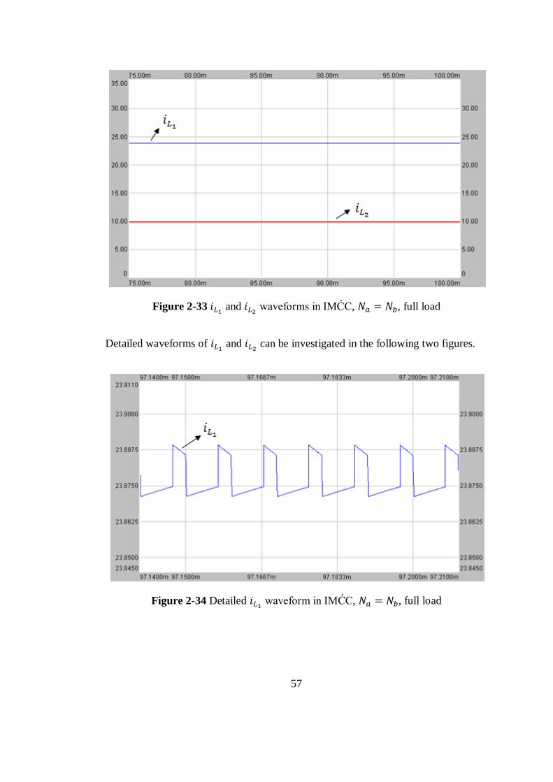
57
Figure 2-33 and
waveforms in IMŠC, , full load
Detailed waveforms of and
can be investigated in the following two figures.
Figure 2-34 Detailed waveform in IMŠC, , full load
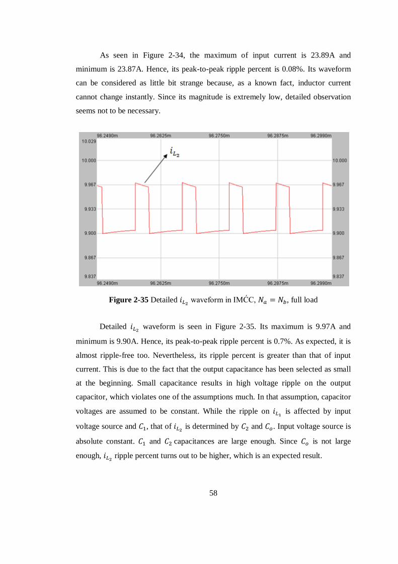
58
As seen in Figure 2-34, the maximum of input current is 23.89A and
minimum is 23.87A. Hence, its peak-to-peak ripple percent is 0.08%. Its waveform
can be considered as little bit strange because, as a known fact, inductor current
cannot change instantly. Since its magnitude is extremely low, detailed observation
seems not to be necessary.
Figure 2-35 Detailed waveform in IMŠC, , full load
Detailed waveform is seen in Figure 2-35. Its maximum is 9.97A and
minimum is 9.90A. Hence, its peak-to-peak ripple percent is 0.7%. As expected, it is
almost ripple-free too. Nevertheless, its ripple percent is greater than that of input
current. This is due to the fact that the output capacitance has been selected as small
at the beginning. Small capacitance results in high voltage ripple on the output
capacitor, which violates one of the assumptions much. In that assumption, capacitor
voltages are assumed to be constant. While the ripple on is affected by input
voltage source and , that of is determined by and . Input voltage source is
absolute constant. and capacitances are large enough. Since is not large
enough, ripple percent turns out to be higher, which is an expected result.
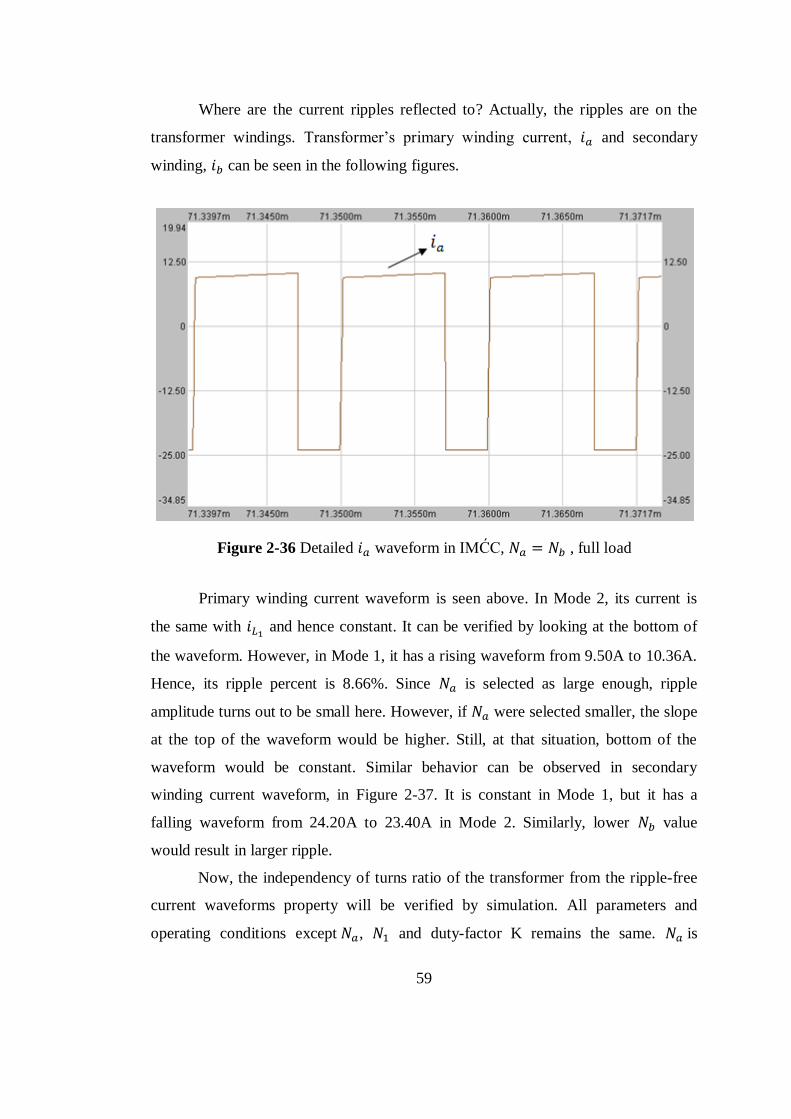
59
Where are the current ripples reflected to? Actually, the ripples are on the
transformer windings. Transformer‟s primary winding current, and secondary
winding, can be seen in the following figures.
Figure 2-36 Detailed waveform in IMŠC, , full load
Primary winding current waveform is seen above. In Mode 2, its current is
the same with and hence constant. It can be verified by looking at the bottom of
the waveform. However, in Mode 1, it has a rising waveform from 9.50A to 10.36A.
Hence, its ripple percent is 8.66%. Since is selected as large enough, ripple
amplitude turns out to be small here. However, if were selected smaller, the slope
at the top of the waveform would be higher. Still, at that situation, bottom of the
waveform would be constant. Similar behavior can be observed in secondary
winding current waveform, in Figure 2-37. It is constant in Mode 1, but it has a
falling waveform from 24.20A to 23.40A in Mode 2. Similarly, lower value
would result in larger ripple.
Now, the independency of turns ratio of the transformer from the ripple-free
current waveforms property will be verified by simulation. All parameters and
operating conditions except , and duty-factor K remains the same. is
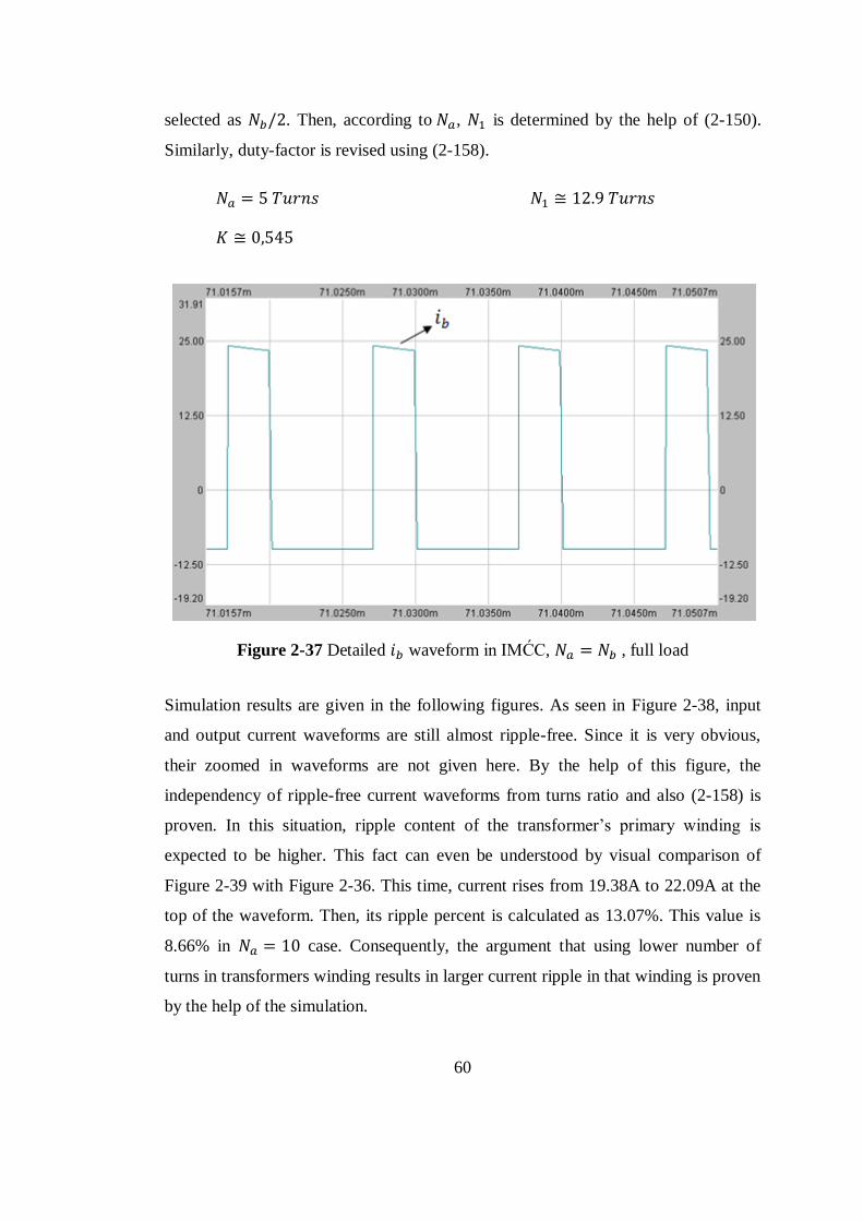
60
selected as . Then, according to , is determined by the help of (2-150).
Similarly, duty-factor is revised using (2-158).
Figure 2-37 Detailed waveform in IMŠC, , full load
Simulation results are given in the following figures. As seen in Figure 2-38, input
and output current waveforms are still almost ripple-free. Since it is very obvious,
their zoomed in waveforms are not given here. By the help of this figure, the
independency of ripple-free current waveforms from turns ratio and also (2-158) is
proven. In this situation, ripple content of the transformer‟s primary winding is
expected to be higher. This fact can even be understood by visual comparison of
Figure 2-39 with Figure 2-36. This time, current rises from 19.38A to 22.09A at the
top of the waveform. Then, its ripple percent is calculated as 13.07%. This value is
8.66% in case. Consequently, the argument that using lower number of
turns in transformers winding results in larger current ripple in that winding is proven
by the help of the simulation.
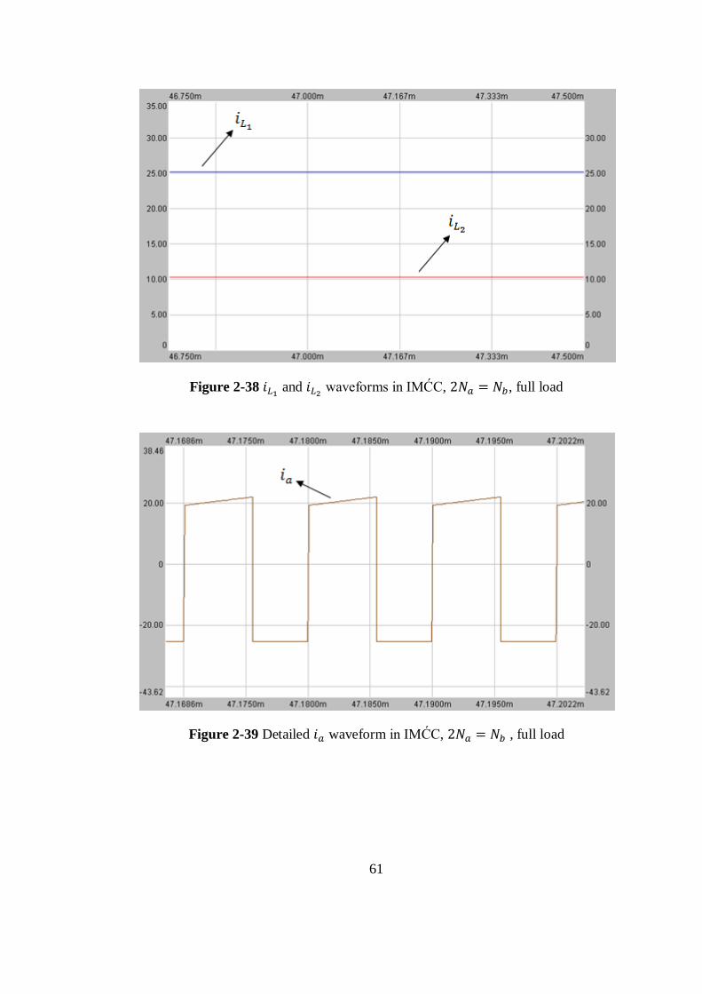
61
Figure 2-38 and
waveforms in IMŠC, , full load
Figure 2-39 Detailed waveform in IMŠC, , full load

62
CHAPTER 3
STEADY-STATE AND DYNAMIC MODEL ANALYSIS
3.1 INTRODUCTION
In this chapter; steady-state model, dynamic model and transfer functions of
coupled-inductor Šuk converter, CIŠC in continuous conduction code, CCM are
obtained utilizing state-space averaging method, SSAM. SSAM is another
contribution of Šuk to power electronics. Detailed explanation about it can be found
in [1]. For the sake of completeness, a summary of SSAM is given in this chapter.
There, the steady-state model, dynamic model and transfer functions are derived in
matrix forms. Therefore, once the state-space model of a circuit is obtained, by
placing the matrices into the final equations give the steady-state model, dynamic
model and transfer functions of the circuit. This process is implemented for the
circuit with ideal and parasitic elements. In the previous chapter, derivatives of two
state-variables –namely and
- are brought to a suitable form for both circuits in
order to use in this chapter.
3.2 STATE-SPACE AVERAGING METHOD
It is widely known that state-space equations of any system can be
represented in the following manner.
(3-1)

63
(3-2)
In continuous time domain and matrices are expected to be
constant for time invariant circuits having only one mode. Any combination of L-C-
R circuit can be given as an example of this kind of circuits. However, switching
circuits are not of that type. Circuits involving diode and/or switch have more than
one mode. A state-space equation set is written while the switch is conducting; but it
is not same with the equation set that is valid while the switch is not conducting. In
that situation, it is not possible to obtain an ordinary state-space equation set. State-
space averaging method, SSAM is a solution of this problem. Equation sets of
different modes are utilized in this method. It briefly argues that:
State-space equation sets pertaining to different modes contribute to the
averaged state-space equation set as much as „their durations/switching
period‟ proportions.
Averaging process causes to lose information about state or output variables
at high frequencies. Averaging is done with respect to switching period.
Hence, switching ripple and the frequencies above the switching frequency is
somehow filtered in this method. At low frequencies, for example below the
one tenth of the switching frequency, it represents the system very
approximately. At the intermediate frequencies, coming closer up to the
switching frequency diverts the system model from the real system.
Normally and matrices consist of L-C-R parameters,
which are generally time-independent. Hence, these matrices are usually
constant. However, averaging process brings duration terms such as
and to the averaged state-space equation
set. Since duty-factor is generally the sole manipulated variable of the
switching circuits and it is time-dependent, averaging process sometimes
make and matrices time-dependent.
This method gives not only steady-state model but also dynamic model. It
presents the steady-state mean values of the variables such as mean value of

64
the capacitor voltage or inductor current. Also, it gives more valuable
information about the dynamic behavior of the system i.e. small signal model.
Utilizing this property, transfer functions of the system can be obtained
easily.
At this point, averaged state-space equation set is assumed to be obtained. All
the following derivations are based on the averaged state-space equation set.
In order to differentiate the steady-state and dynamic models, all matrices are
divided into two parts as „mean values‟ and „perturbed values‟.
(3-3)
(3-4)
Capitals such as and are constant terms and represent the dc levels at that
operating point. Terms with „~‟ such as and are time-dependent and
represent the small signal part at that operating point. As a first step, (3-3)-(3-4) are put
into (3-1)-(3-2).
(3-5)
(3-6)
and rearranging them gives:
(3-7)
(3-8)
At this point, the following assumption highly simplifies the analysis. Actually, it can
be considered as a reasonable assumption for small signal analysis.
65
Assumption 3-1: Magnitudes of the capitals are much larger than that of the terms
with „~‟.
Hence, neglecting second-order small-signal terms in (3-7)-(3-8) gives;
(3-9)
(3-10)
in which steady-state and dynamic models can be separated as;
Steady-State Model:
(3-11)
(3-12)
Dynamic Model:
(3-13)
(3-14)
As mentioned earlier, transfer functions of the system can be obtained by
applying Laplace transformation to dynamic model. Since the terms with „~‟
represent the small signal ac part, initial conditions can be taken as zero. Actually,
they are included in dc parts.
(3-15)
(3-16)
At this step, can be obtained by using (3-15).

66
(3-17)
Then, is obtained in terms of the known quantities and inputs by using (3-16)
and (3-17) as;
(3-18)
3.3 ANALYSIS OF COUPLED-INDUCTOR ĆUK CONVERTER,
CIĆC WITH IDEAL ELEMENTS
In this section, steady-state and dynamic model of CIŠC in continuous
conduction mode, CCM are obtained. Using dynamic model, transfer functions are
also derived. In [2], all these derivations are present for basic Šuk converter. As
expected, they are highly different than those of CIŠC. Therefore, it is necessary to
derive them for coupled-inductor case. Besides, in [2], load –namely the output
current- is not considered as a time varying input to the converter. Hence, it is not
possible to obtain a transfer function reference to the output current there. Here, the
output current is considered as a time varying input to the converter.
The circuit schematic of coupled-inductor Šuk converter with ideal elements
is seen in Figure 3-1. Directions of the currents are also shown.
Figure 3-1 Circuit schematic of CIŠC with ideal elements and directions of currents
included

67
Since there are four energy storage elements, four state-variables exist. They are
currents in inductors and voltages in capacitors. State-space equations are written in
terms of these variables, inputs and outputs. In this work, input current and output
voltage are chosen as outputs.
3.3.1 State-Space Equation Set in Mode 1
The equivalent circuit in Mode 1 is as shown in Figure 3-2, where the switch
is on.
Figure 3-2: Equivalent circuit schematic of CIŠC with ideal elements in Mode 1
Burrowing the derivatives of and
in Mode 1 derived in CHAPTER 2 as (2-27)
and (2-28) and using them here directly as (3-19) and (3-20), we have;
(3-19)
(3-20)
Now, derivatives of capacitor voltages should be obtained.
For :
(3-21)

68
(3-22)
(3-23)
is obtained in terms of state-variables. Similar process is applied to
.
For :
(3-24)
(3-25)
(3-26)
Using (3-19), (3-20), (3-23) and (3-26); the following equation matrix is obtained.
(3-27)
As it is seen clearly, input voltage and output current are inputs to the converter.
Duty-factor of the switch is defined at this stage. Symbol represents the duty-
factor.
(3-28)
As mentioned earlier, multiplying the matrices with their durations gives their
contribution to the averaged matrices. Matrix or simply for Mode 1 is defined
as (t) or simply . The same argument applies to other matrices, so that;

69
(3-29)
(3-30)
is written similarly. As mentioned earlier, outputs of the system are selected as
the output voltage and the input current, which equals .
(3-31)
The following matrices are obtained.
(3-32)
(3-33)
3.3.2 State-Space Equation Set in Mode 2
The equivalent circuit in Mode 2 is shown in Figure 3-3, with the switch OFF
and the diode ON. Similar arguments followed for and
in Mode 1 apply also
in Mode 2. (2-32) and (2-33) can be used here directly as;
(3-34)
(3-35)

70
Figure 3-3: Equivalent circuit schematic of CIŠC with ideal elements in Mode 2
For :
(3-36)
(3-37)
For :
It is the same with that in Mode 1.
(3-38)
Using (3-34), (3-35), (3-37) and (3-39); the following equation matrix is obtained.
(3-39)
This time, the normalized duration with respect to the switching period is .
Hence, we have;

71
(3-40)
(3-41)
is the same with that in Mode 1. Likewise, the following matrices are obtained.
(3-42)
(3-43)
3.3.3 Averaging of Matrices in Mode 1 and Mode 2
Averaged matrices are represented by and
in the following manner.
(3-44)
(3-45)
(3-46)
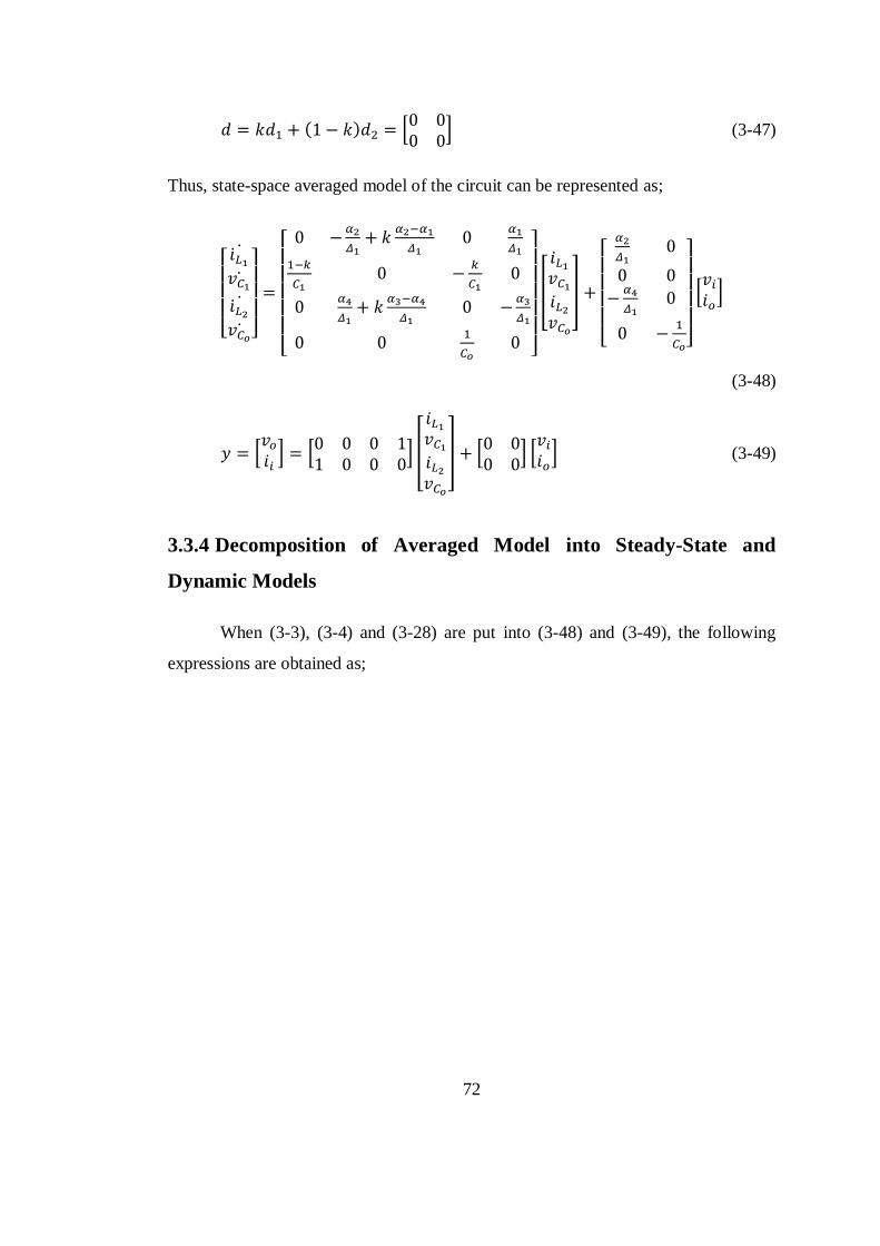
72
(3-47)
Thus, state-space averaged model of the circuit can be represented as;
(3-48)
(3-49)
3.3.4 Decomposition of Averaged Model into Steady-State and
Dynamic Models
When (3-3), (3-4) and (3-28) are put into (3-48) and (3-49), the following
expressions are obtained as;

73
(3-50)
(3-51)
Then, the matrices in (3-11)-(3-14) can be extracted from (3-50) and (3-51),
respectively as;
(3-52)
(3-53)

74
(3-54)
(3-55)
(3-56)
(3-57)
(3-58)
(3-59)
(3-60)
3.3.5 Steady-State Model
The static model is given in (3-11) and (3-12). Utilizing the matrices above,
the following matrix equations are obtained.

75
(3-61)
(3-62)
(3-62) is just given for the sake of completeness. Required information is extracted
from (3-61) as;
First row:
(3-63)
(3-64)
Second row:
(3-65)
(3-66)
Third row:
(3-67)
(3-68)
Fourth row:
(3-69)

76
(3-70)
Some meaningful results can be inferred from (3-64), (3-66), (3-68) and (3-70).
(3-70) says that mean value of current, is equal to mean value of
the output current, . Since mean value of current, is zero at
steady-state, this result is consistent and meaningful.
From (3-64) and (3-68), the following equation is obtained. Note that
is equal to .
(3-71)
(3-71) gives the relationship between the mean values of the input
voltage, the output voltage and the duty-factor. It is the standard
input/output relationship met in buck-boost structures. Moreover, the
following equation is obtained from (3-64) or (3-68) by substitution of
into the equations. can be extracted from (3-71).
(3-72)
Mean value of the voltage on is equal to the sum of the mean values of
the input and the output voltages. This is another known relationship of
the basic Šuk converter.
From (3-66) input-to-output power equality is inferred. can be
replaced with mean value of the input current, . As inferred earlier, is
equal to .
(3-73)
Multiplication of (3-71) and (3-73) gives input-to-output power equality
so that,
(3-74)

77
Since all electrical elements are assumed to be ideal, the efficiency turns
out to be 100%. Again, this is a consistent result.
3.3.6 Dynamic Model and Transfer Functions
The dynamic model is given in (3-13) and (3-14). Since the aim is to get the
transfer functions, the use of (3-18) will be more proper. Simplification can be
applied before using it, because most of the matrices are constant. The simplified
version of (3-18) is given in (3-75).
(3-75)
will be obtained step by step. Substituting (3-52) and (3-60) into (3-75) gives
(3-76);
(3-76)
where

78
Then,
(3-77)
where
(3-78)
Next step is to obtain .
(3-79)
Laplace transformations of and are simply and because initial
conditions are already included in and .
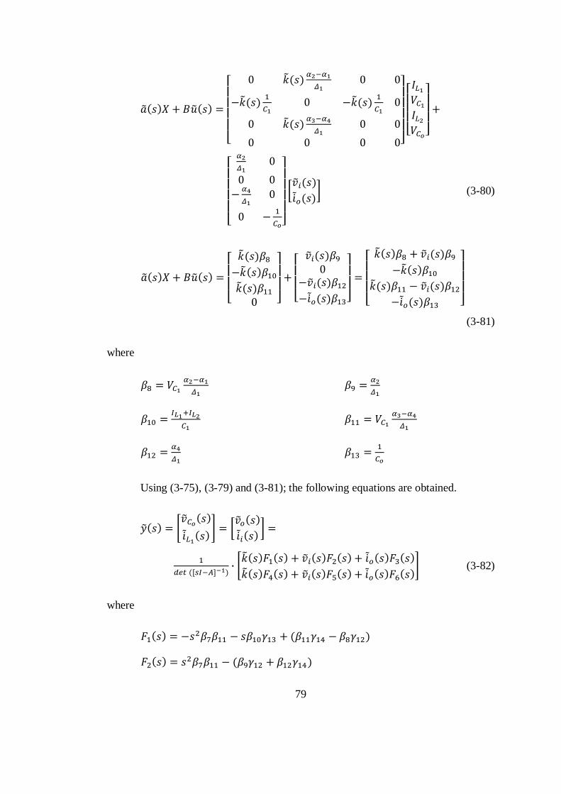
79
(3-80)
(3-81)
where
Using (3-75), (3-79) and (3-81); the following equations are obtained.
(3-82)
where

80
There are six transfer functions to be inferred from (3-82). The outputs are
and
; and the inputs are , and . At this
point linearity assumption is necessary. In small signal model, perturbations around
operating point with small magnitudes are considered not to violate the linearity of
the small signal model. By the help of this assumption, superposition theorem can be
applied to (3-82). As a result, the following six transfer functions can be defined.
Duty Factor to Output Voltage Transfer Function:
(3-83)
Input Voltage to Output Voltage Transfer Function:
(3-84)
Output Current to Output Voltage Transfer Function:
(3-85)

81
Duty Factor to Input Current Transfer Function:
(3-86)
Input Voltage to Input Current Transfer Function:
(3-87)
Output Current to Input Current Transfer Function:
(3-88)
3.3.7 Verification of the Transfer Functions
In this section, the calculated transfer functions of coupled-inductor Šuk
converter with ideal elements through (3-83)-(3-88) are verified by simulations. Two
different simulation tools are benefited for this purpose. One of them is Matlab. In
this simulation tool, the calculated transfer functions are used as a transfer function
block. Small step disturbances in the variables appearing in the denominator of the
transfer functions are applied to the transfer functions and the dynamic responses are
observed in time domain. Second type of simulations uses Simplorer as a simulation
tool. In this simulation group, process circuit model is used instead of the transfer
functions. Only the circuit model is present. The same small step disturbances are
applied to the circuit model and the dynamic responses are observed, which are

82
naturally in time domain. If the results of both simulations turn out to be the same,
one may consider that the transfer function under investigation is valid.
At this point, it is useful to highlight one point. Since the transfer functions
are composed of labels, it is not easy to see that they include operating point
parameters such as ,
, ,
and . That is, transfer functions are specific to
the operating point. For this reason, transfer functions are calculated with respect to
operating point. As the operating point, the fourth end operating point ( ,
, full load) is selected.
Verification of :
In Figure 3-4, step response of the duty-factor-to-output voltage transfer
function is given. Horizontal axis is in seconds and vertical axis is in volts.
As a step disturbance, 0.0025 increase in duty-factor is utilized. Mathematically,
Figure 3-4 is the plot of the following function in time domain.
It is plotted in Matlab with the following input parameters. , , , , ,
and are the parameters of the practically implemented circuit. , ,
and
are the parameters taken from the simulation which is aimed to be performed at the
fourth end operating point. As it is understood, small deviation in the simulation is
also reflected to the transfer function for a better comparison.
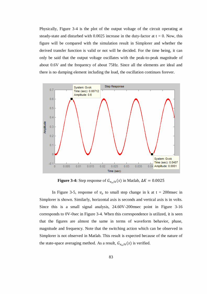
83
Physically, Figure 3-4 is the plot of the output voltage of the circuit operating at
steady-state and disturbed with 0.0025 increase in the duty-factor at t = 0. Now, this
figure will be compared with the simulation result in Simplorer and whether the
derived transfer function is valid or not will be decided. For the time being, it can
only be said that the output voltage oscillates with the peak-to-peak magnitude of
about 0.6V and the frequency of about 75Hz. Since all the elements are ideal and
there is no damping element including the load, the oscillation continues forever.
Figure 3-4: Step response of in Matlab,
In Figure 3-5, response of to small step change in k at t = 200msec in
Simplorer is shown. Similarly, horizontal axis is seconds and vertical axis is in volts.
Since this is a small signal analysis, 24.60V-200msec point in Figure 3-16
corresponds to 0V-0sec in Figure 3-4. When this correspondence is utilized, it is seen
that the figures are almost the same in terms of waveform behavior, phase,
magnitude and frequency. Note that the switching action which can be observed in
Simplorer is not observed in Matlab. This result is expected because of the nature of
the state-space averaging method. As a result, is verified.
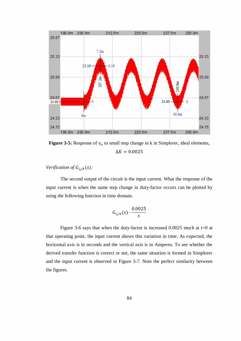
84
Figure 3-5: Response of to small step change in k in Simplorer, ideal elements,
Verification of :
The second output of the circuit is the input current. What the response of the
input current is when the same step change in duty-factor occurs can be plotted by
using the following function in time domain.
Figure 3-6 says that when the duty-factor is increased 0.0025 much at t=0 at
that operating point, the input current shows this variation in time. As expected, the
horizontal axis is in seconds and the vertical axis is in Amperes. To see whether the
derived transfer function is correct or not, the same situation is formed in Simplorer
and the input current is observed in Figure 3-7. Note the perfect similarity between
the figures.
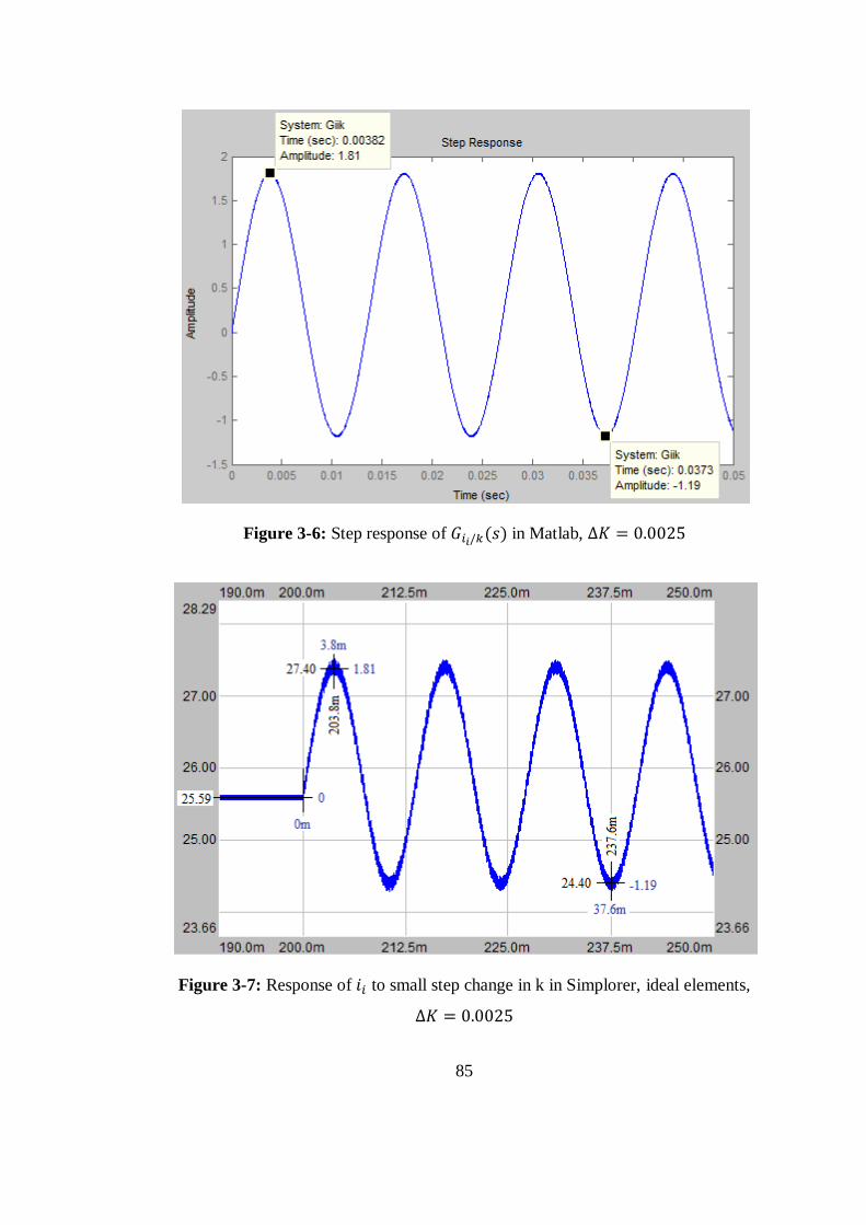
85
Figure 3-6: Step response of in Matlab,
Figure 3-7: Response of to small step change in k in Simplorer, ideal elements,

86
Verification of :
The response of the output voltage when 0.1V step change in input voltage
occurs is plotted in Figure 3-8 by using the following function in time domain.
Figure 3-8: Step response of in Matlab,
The corresponding waveform in Simplorer is presented in Figure 3-9. is
validated in this way.
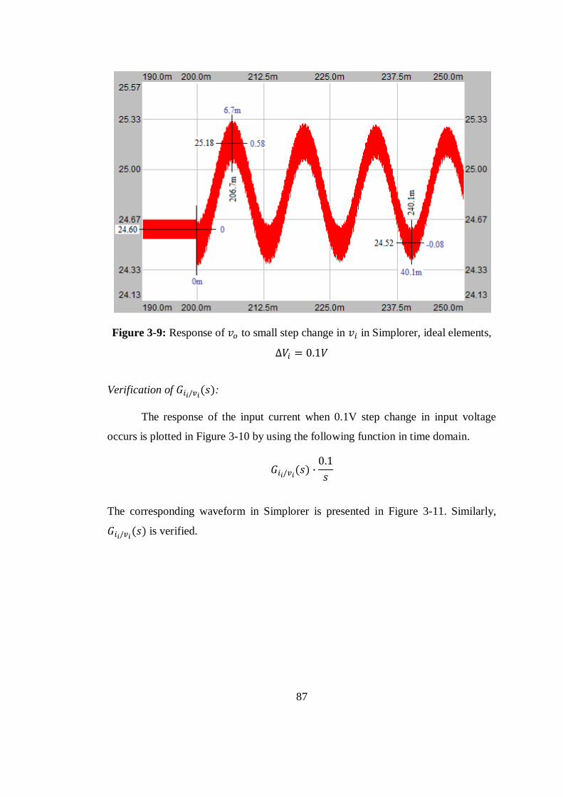
87
Figure 3-9: Response of to small step change in in Simplorer, ideal elements,
Verification of :
The response of the input current when 0.1V step change in input voltage
occurs is plotted in Figure 3-10 by using the following function in time domain.
The corresponding waveform in Simplorer is presented in Figure 3-11. Similarly,
is verified.
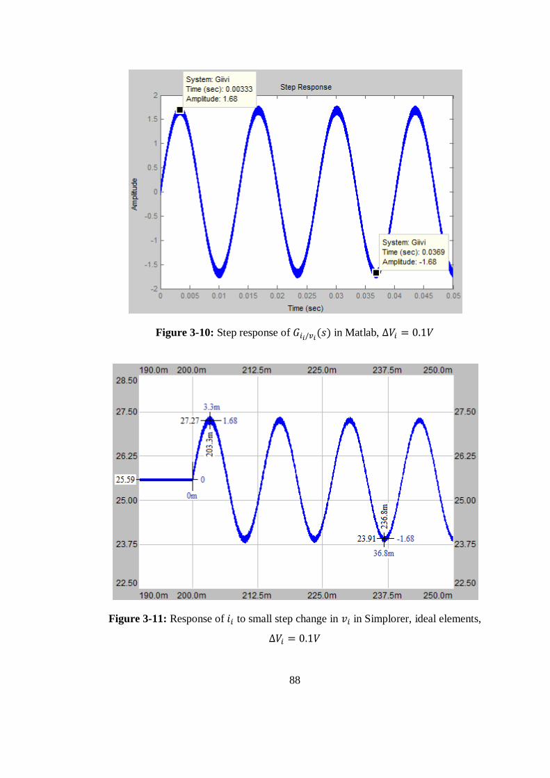
88
Figure 3-10: Step response of in Matlab,
Figure 3-11: Response of to small step change in in Simplorer, ideal elements,
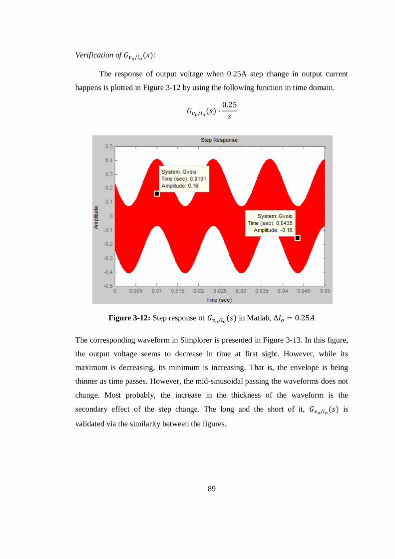
89
Verification of :
The response of output voltage when 0.25A step change in output current
happens is plotted in Figure 3-12 by using the following function in time domain.
Figure 3-12: Step response of in Matlab,
The corresponding waveform in Simplorer is presented in Figure 3-13. In this figure,
the output voltage seems to decrease in time at first sight. However, while its
maximum is decreasing, its minimum is increasing. That is, the envelope is being
thinner as time passes. However, the mid-sinusoidal passing the waveforms does not
change. Most probably, the increase in the thickness of the waveform is the
secondary effect of the step change. The long and the short of it, is
validated via the similarity between the figures.
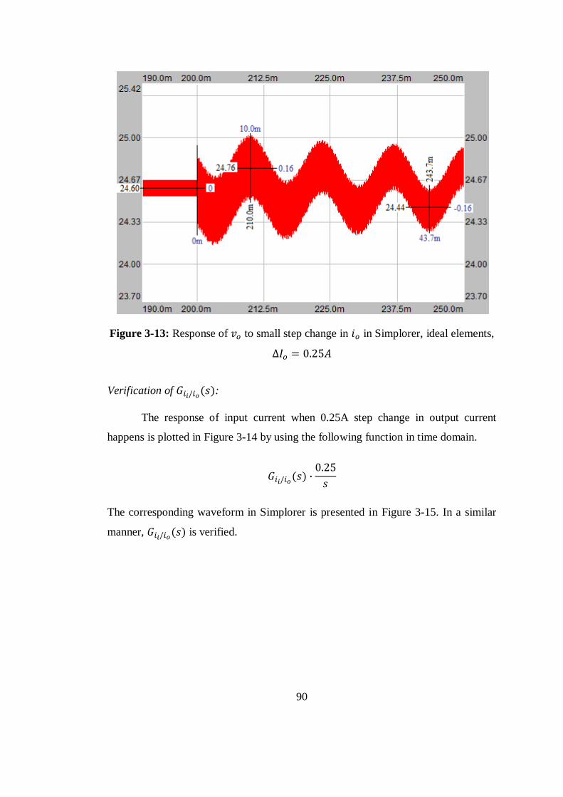
90
Figure 3-13: Response of to small step change in in Simplorer, ideal elements,
Verification of :
The response of input current when 0.25A step change in output current
happens is plotted in Figure 3-14 by using the following function in time domain.
The corresponding waveform in Simplorer is presented in Figure 3-15. In a similar
manner, is verified.
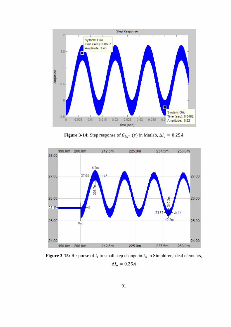
91
Figure 3-14: Step response of in Matlab,
Figure 3-15: Response of to small step change in in Simplorer, ideal elements,
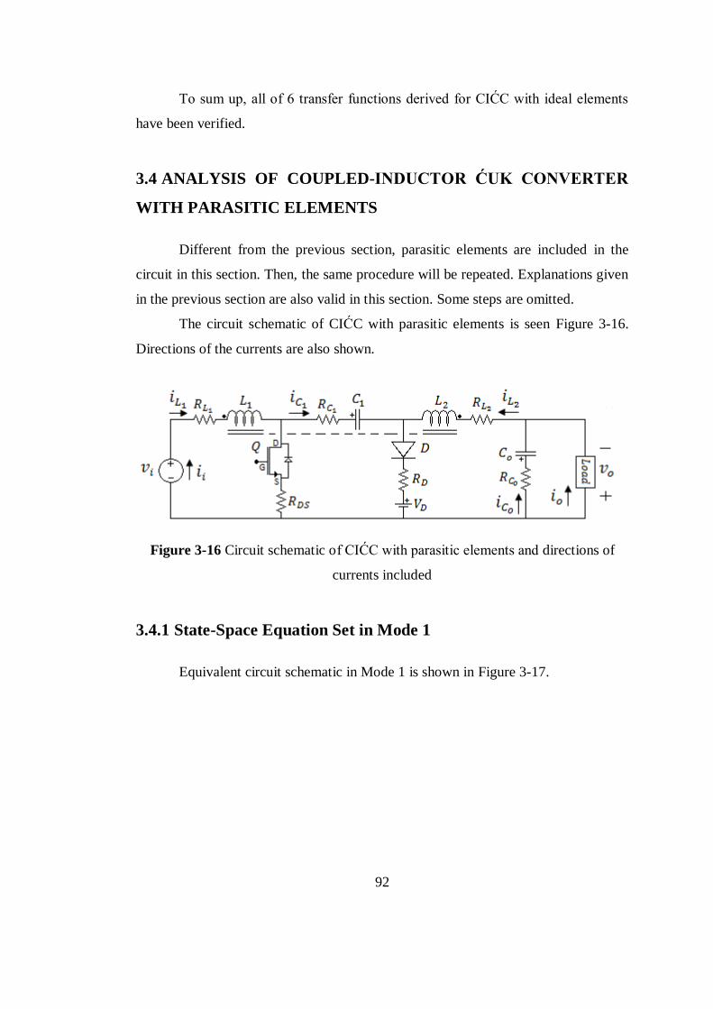
92
To sum up, all of 6 transfer functions derived for CIŠC with ideal elements
have been verified.
3.4 ANALYSIS OF COUPLED-INDUCTOR ĆUK CONVERTER
WITH PARASITIC ELEMENTS
Different from the previous section, parasitic elements are included in the
circuit in this section. Then, the same procedure will be repeated. Explanations given
in the previous section are also valid in this section. Some steps are omitted.
The circuit schematic of CIŠC with parasitic elements is seen Figure 3-16.
Directions of the currents are also shown.
Figure 3-16 Circuit schematic of CIŠC with parasitic elements and directions of
currents included
3.4.1 State-Space Equation Set in Mode 1
Equivalent circuit schematic in Mode 1 is shown in Figure 3-17.

93
Figure 3-17 Equivalent circuit schematic of CIŠC with parasitic elements (directions
of currents included) in Mode 1
Burrowing the derivatives of and
in Mode 1 derived in CHAPTER 2 as (2-80)
and (2-81) and using them here directly as (3-89) and (3-90), we have;
(3-89)
(3-90)
where
Note that and
terms have been added to the equations different from the ideal
case. Besides, the coefficients of other terms have changed.
Next step is to obtain derivatives of capacitor voltages. Before proceeding
further, an important point should be considered: Equivalent series resistance, ESRs
of the capacitors are included in the element model. In this situation, capacitor
voltage would normally be expected to include the voltage drop on ESR.
However, state-space averaging method, SSAM is based on state-variables, which

94
are selected as the variables representing the energy content of the energy storing
elements. For capacitors, state-variables are the voltages on them. Including the ESR
voltage drops on capacitor voltages would be wrong because it would not give the
right information about its stored energy. Therefore, in the following equations,
represents the voltage of ideal capacitor and not the voltage drop on ESR.
Actually, the same argument applies to other parasitic elements, as well.
For :
(3-91)
where
For :
(3-92)
where
Then the following equation matrix is obtained. Note that the dimensions of matrix
and vector increase. This modification is needed in Mode 2 and does not affect this
mode practically. Still, the modification is applied here for the consistency in
dimensions of the matrices. The reason of this change will be explained in Mode 2
analysis.
(3-93)
The following matrices are obtained by addition of duty-factor. Since these matrices
are valid in Mode 1, their elements are multiplied by .

95
(3-94)
(3-95)
is written in the following manner. Before that, should be obtained because it
seems to be different in this analysis compared to that in the previous analysis.
remains the same.
(3-96)
(3-97)
(3-98)
where
As a result, the following matrices are obtained as;
(3-99)
(3-100)
3.4.2 State-Space Equation Set in Mode 2
Equivalent circuit in Mode 2 is as shown in Figure 3-18.
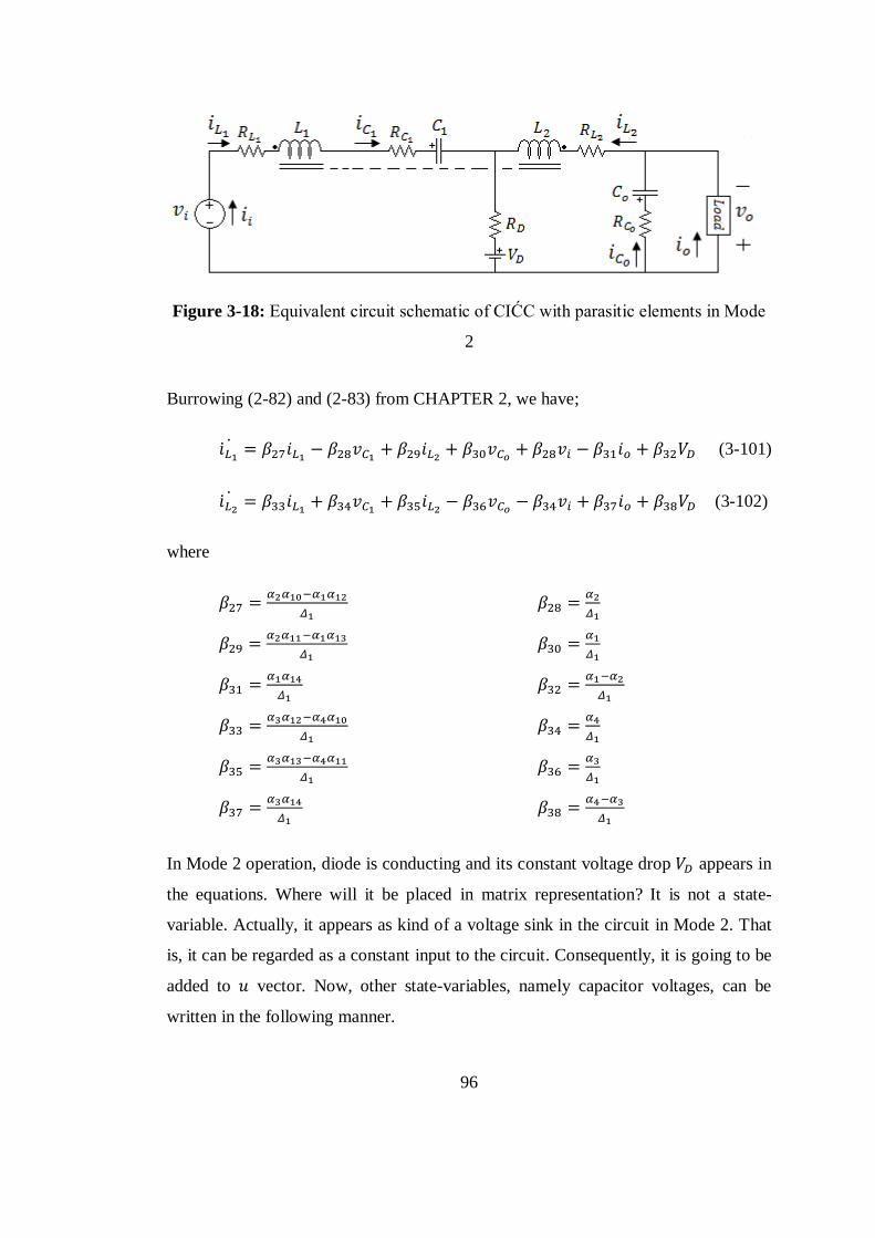
96
Figure 3-18: Equivalent circuit schematic of CIŠC with parasitic elements in Mode
2
Burrowing (2-82) and (2-83) from CHAPTER 2, we have;
(3-101)
(3-102)
where
In Mode 2 operation, diode is conducting and its constant voltage drop appears in
the equations. Where will it be placed in matrix representation? It is not a state-
variable. Actually, it appears as kind of a voltage sink in the circuit in Mode 2. That
is, it can be regarded as a constant input to the circuit. Consequently, it is going to be
added to vector. Now, other state-variables, namely capacitor voltages, can be
written in the following manner.

97
For :
(3-103)
For :
(3-104)
The following equation is obtained.
(3-105)
In Mode 2, the duration is . Hence,
(3-106)
(3-107)
is the same with that in Mode 1. Thus,
(3-108)
(3-109)

98
3.4.3 Averaging of Matrices in Mode 1 and Mode 2
Averaged matrices of and are obtained as
follows;
(3-110)
(3-111)
(3-112)
(3-113)
As a result, state-space averaged model of the circuit can be represented in
(3-114) and (3-115).
(3-114)

99
(3-115)
3.4.4 Decomposition of Averaged Model into Steady-State and
Dynamic Models
Separation is done in the same way followed in Section 3.3.4.
(3-116)
where

100
(3-117)
Individual matrices can be extracted from (3-116) and (3-117) in the following
manner. The same matrices with the ones in Section 3.3.4 are excluded in order not
to repeat.
(3-118)
(3-119)
(3-120)
(3-121)

101
Note that is taken as zero because diode forward voltage drop is assumed to be
constant.
(3-122)
(3-123)
3.4.5 Steady-State Model
Utilizing the matrices above, the following matrix equations are obtained.
(3-124)
(3-125)
First row of (3-124):
(3-126)
Using (3-135):
(3-127)
This result will be used later.
Second row of (3-124):
(3-128)
(3-129)

102
It is the same result with the case of ideal electrical elements. It is not affected by the
parasitic elements.
Third row of (3-124):
(3-130)
(3-131)
Fourth row of (3-124):
(3-132)
(3-133)
This result remains the same too.
First row of (3-115):
(3-134)
Using (3-133):
(3-135)
Even though ESR of the output capacitance makes the instantaneous output voltage
differs from the voltage of the output capacitance, their mean values turn out to be
the same, which is an expected result.
Second row (3-115):
(3-136)
This is just a trivial result.
(3-127) and (3-131) may be simplified as in the case of ideal elements.
However, those equations are too complex to be handled successfully. Hence, they
are utilized only for efficiency calculation. By equating both equations, the
relationship between and can be derived.

103
(3-137)
where
Then, the efficiency can be calculated as follows;
Using (3-129), (3-133) and (3-137):
and
can be written in terms of .
Further simplification gives the final efficiency expression in (3-138). It will be used
and investigated in the design chapter. However, a clarification may be needed at this
step: terms need not to be positive. Moreover, they should have signs such that
and terms decrease the efficiency.
(3-138)
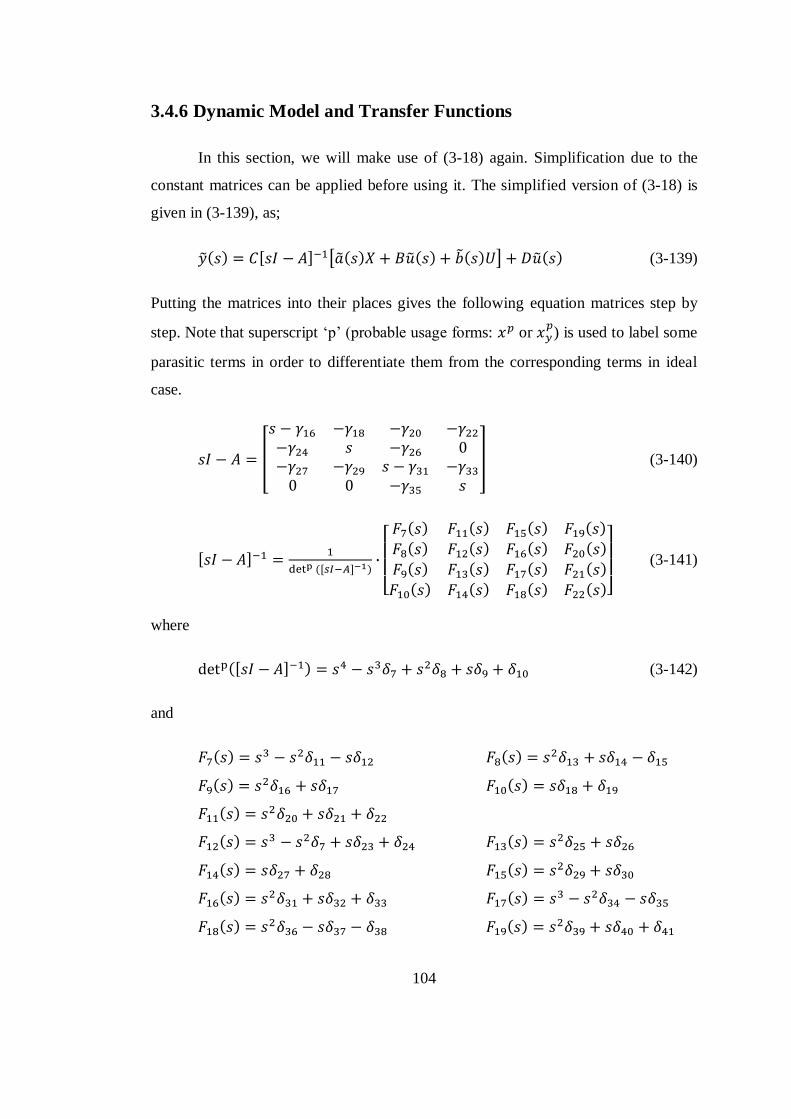
104
3.4.6 Dynamic Model and Transfer Functions
In this section, we will make use of (3-18) again. Simplification due to the
constant matrices can be applied before using it. The simplified version of (3-18) is
given in (3-139), as;
(3-139)
Putting the matrices into their places gives the following equation matrices step by
step. Note that superscript „p‟ (probable usage forms: or ) is used to label some
parasitic terms in order to differentiate them from the corresponding terms in ideal
case.
(3-140)
(3-141)
where
(3-142)
and

105
and
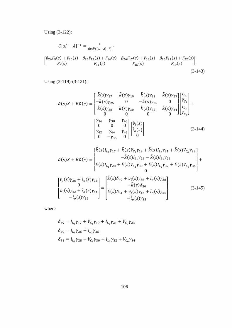
106
Using (3-122):
(3-143)
Using (3-119)-(3-121):
(3-144)
(3-145)
where
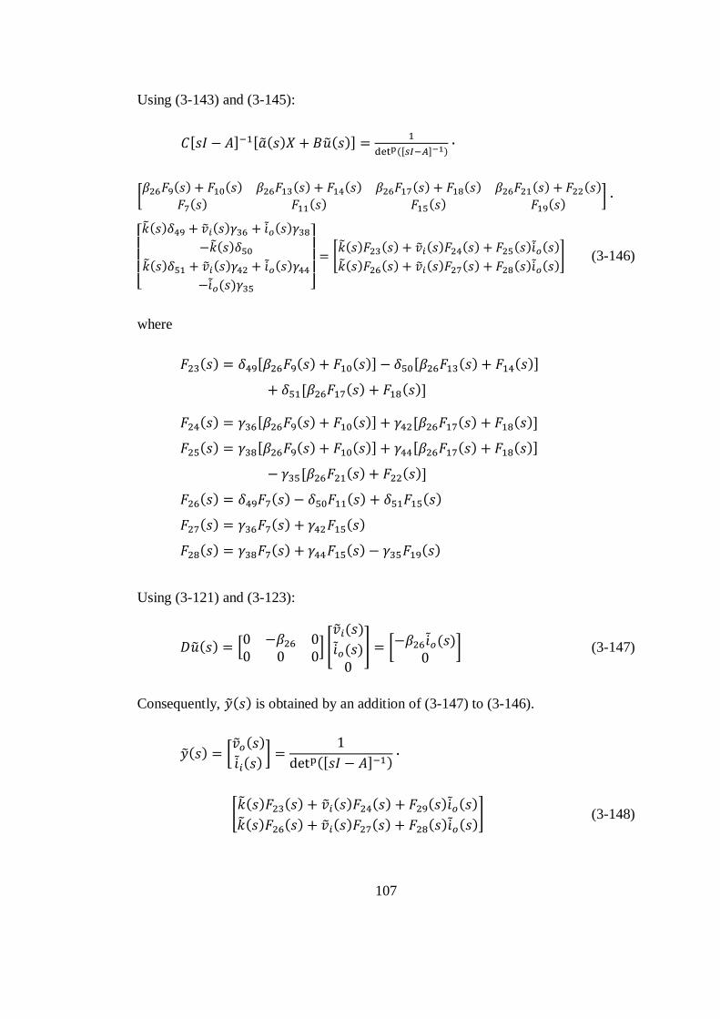
107
Using (3-143) and (3-145):
(3-146)
where
Using (3-121) and (3-123):
(3-147)
Consequently, is obtained by an addition of (3-147) to (3-146).
(3-148)

108
where
As in the case of ideal elements, again there are six transfer functions to be
inferred from (3-148).
Duty Factor to Output Voltage Transfer Function:
(3-149)
Input Voltage to Output Voltage Transfer Function:
(3-150)
Output Current to Output Voltage Transfer Function:
(3-151)
Duty Factor to Input Current Transfer Function:
(3-152)
Input Voltage to Input Current Transfer Function:
(3-153)
Output Current to Input Current Transfer Function:
(3-154)
It is not possible to express the transfer functions in explicit form due to the
crowd of the terms. However, it can be said that each transfer function is the division

109
of two polynomials in s. While the order of the numerator is at most 3, that of the
denominator is constant at 4.
3.4.7 Verification of the Transfer Functions
The same procedure followed for coupled-inductor Šuk converter, CIŠC with
ideal elements will be repeated for CIŠC with parasitic elements in this section.
Parameters of parasitic elements are taken from the final parameters in the design
section. That is to say, they belong to the implemented circuit. Besides, calculations
and simulations are realized at the same operating point in the ideal case.
Verification of
:
In Figure 3-19, step response of the duty-factor-to-output voltage transfer
function
is given. Horizontal axis is in seconds and vertical axis is in volts.
As a step disturbance, again, 0.0025 increase in duty-factor is utilized.
Mathematically, Figure 3-19 is the plot of the following function in time domain.
It is plotted in Matlab with the following input parameters as an addition to
parameters used in the verification of the transfer functions in ideal case. , ,
,
, and are the parameters of the practically implemented circuit.
is
the parameter taken from the simulation which is aimed to be performed at the fourth
end operating point.
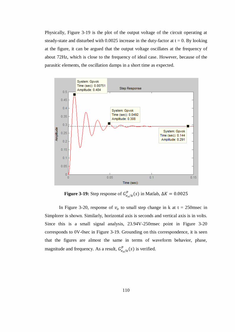
110
Physically, Figure 3-19 is the plot of the output voltage of the circuit operating at
steady-state and disturbed with 0.0025 increase in the duty-factor at t = 0. By looking
at the figure, it can be argued that the output voltage oscillates at the frequency of
about 72Hz, which is close to the frequency of ideal case. However, because of the
parasitic elements, the oscillation damps in a short time as expected.
Figure 3-19: Step response of
in Matlab,
In Figure 3-20, response of to small step change in k at t = 250msec in
Simplorer is shown. Similarly, horizontal axis is seconds and vertical axis is in volts.
Since this is a small signal analysis, 23.94V-250msec point in Figure 3-20
corresponds to 0V-0sec in Figure 3-19. Grounding on this correspondence, it is seen
that the figures are almost the same in terms of waveform behavior, phase,
magnitude and frequency. As a result,
is verified.
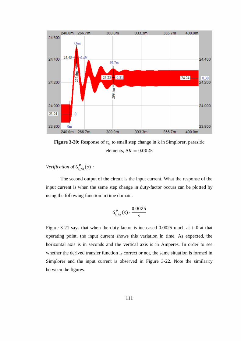
111
Figure 3-20: Response of to small step change in k in Simplorer, parasitic
elements,
Verification of
:
The second output of the circuit is the input current. What the response of the
input current is when the same step change in duty-factor occurs can be plotted by
using the following function in time domain.
Figure 3-21 says that when the duty-factor is increased 0.0025 much at t=0 at that
operating point, the input current shows this variation in time. As expected, the
horizontal axis is in seconds and the vertical axis is in Amperes. In order to see
whether the derived transfer function is correct or not, the same situation is formed in
Simplorer and the input current is observed in Figure 3-22. Note the similarity
between the figures.
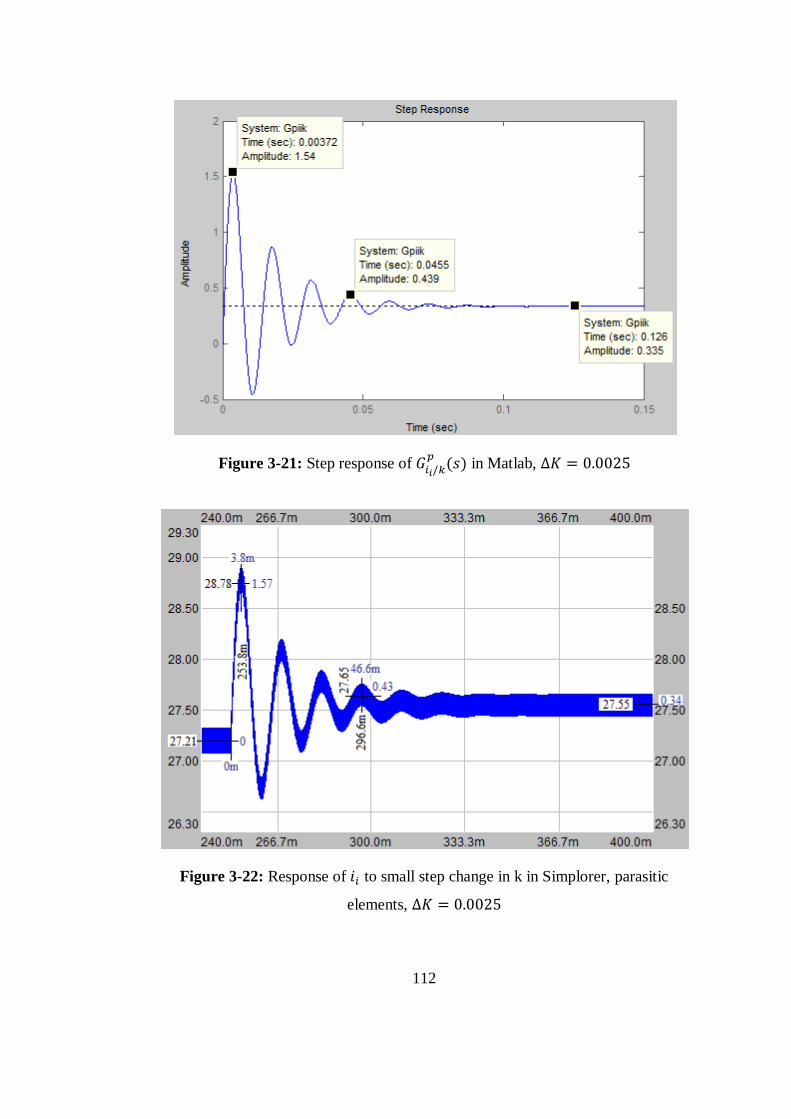
112
Figure 3-21: Step response of
in Matlab,
Figure 3-22: Response of to small step change in k in Simplorer, parasitic
elements,
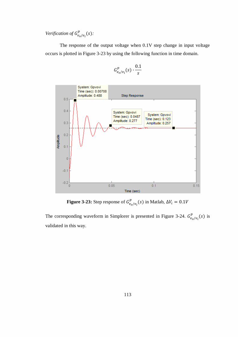
113
Verification of
:
The response of the output voltage when 0.1V step change in input voltage
occurs is plotted in Figure 3-23 by using the following function in time domain.
Figure 3-23: Step response of
in Matlab,
The corresponding waveform in Simplorer is presented in Figure 3-24.
is
validated in this way.

114
Figure 3-24: Response of to small step change in in Simplorer, parasitic
elements,
Verification of
:
The response of the input current when 0.1V step change in input voltage
occurs is plotted in Figure 3-25 by using the following function in time domain.
The corresponding waveform in Simplorer is introduced in Figure 3-26. In this
manner,
is also verified.
115
Figure 3-25: Step response of
in Matlab,
Figure 3-26: Response of to small step change in in Simplorer, parasitic
elements,
116
Verification of
:
The response of output voltage when 0.25A step change in output current
happens is plotted in Figure 3-27 by using the following function in time domain.
Figure 3-27: Step response of
in Matlab,
The corresponding waveform in Simplorer is given in Figure 3-28. By grounding on
the sufficient similarity between the figures,
is verified.
117
Figure 3-28: Response of to small step change in in Simplorer, parasitic
elements,
Verification of
:
The response of input current when 0.25A step change in output current
happens is plotted in Figure 3-29 by using the following function in time domain.
The corresponding waveform in Simplorer is shown in Figure 3-30. Likewise,
is verified.
In conclusion, all of 6 transfer functions derived for CIŠC with parasitic
elements have been validated.
118
Figure 3-29: Step response of
in Matlab,
Figure 3-30: Response of to small step change in in Simplorer, parasitic
elements,

119
CHAPTER 4
DESIGN OF A COUPLED-INDUCTOR CUK
CONVERTER
4.1 INTRODUCTION
This chapter comprises of two main topics. In the first topic, operational
requirements of the converter are defined. Where it will be used, for what purpose it
will be utilized and what are expected from the converter are given in details. Then,
based on these data, technical requirements are determined. Second topic is the
selection or design of the circuit components according to the technical requirements
in the first topic. Then, the design will be verified by simulations or experimental
tests wherever they are needed and possible.
4.2 OPERATIONAL REQUIREMENTS OF THE CONVERTER
Coupled-inductor Šuk converter implemented in this work will be used
mainly in one of the projects in ASELSAN. Therefore, the design criteria and
parameters are determined by the project specifications. Before determining the
design criteria, possible operating conditions must be considered at this point.
This converter will be used in the vehicle configuration of portable military
equipment or military system. This equipment has two configurations: man-portable
configuration and vehicle configuration. In man-portable configuration, the

120
equipment is powered only by lithium-ion battery pack. According to the energy
capacity of the battery pack, operating time of the equipment is determined. In
vehicle configuration, again lithium-ion battery pack is utilized but it is not the
unique energy source in this configuration. There exists another energy source,
namely the battery group of the vehicle. It is desired to draw as much power as
possible from this source to increase the operating time. Energizing the equipment
only by the battery group of the vehicle, thereby eliminating the need for lithium-ion
battery pack and providing a very long operating time compared to lithium-ion
battery pack case is aimed. At this point, an interface problem arises: Input voltage
level of the equipment does not match that of the vehicle battery. Actually, there are
vehicles having different dc buses at different voltage levels in practice. The
interface relating current levels is more sophisticated than that of voltage levels.
Power is another problematic issue. Therefore, a dc-to-dc converter having voltage,
current and/or power control modes is considered as a necessary element in the
solution of this problem. The details are given in the following paragraphs.
In vehicle configuration, the converter will be fed by a vehicle battery and
supply power to the equipment. Feeding of the converter can be realized in two
ways:
direct connection to vehicle battery,
connection to vehicle battery through vehicle cigarette-lighter adapter
(indirect connection).
This connection difference stems from the current carrying capability of the
interconnecting elements. As it is assumed, in direct connection to the battery,
current carrying capability depends on the input cable of the converter. That is,
current limit is controllable. More current can be drawn by using a thick cable.
However, cigarette lighter adapters have generally low current limits because they
are not designed to supply much power.
If direct battery connection is feasible, the converter is desired to supply its
rated power to the military equipment, or the load. The maximum power
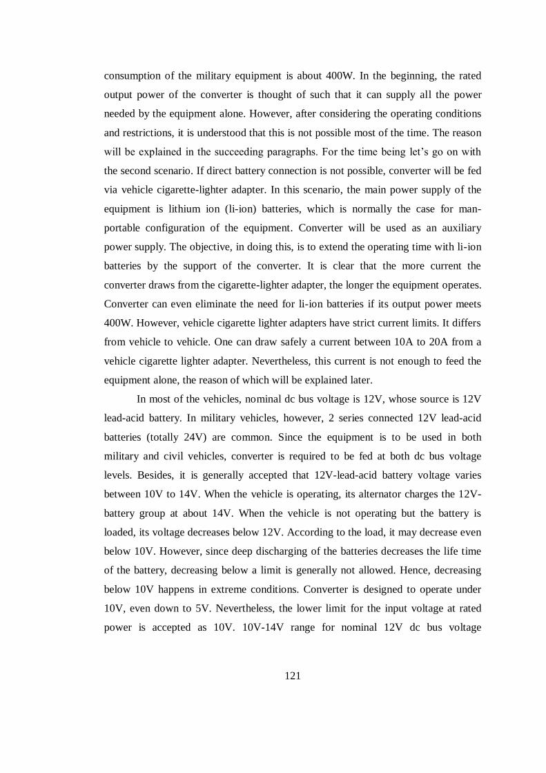
121
consumption of the military equipment is about 400W. In the beginning, the rated
output power of the converter is thought of such that it can supply all the power
needed by the equipment alone. However, after considering the operating conditions
and restrictions, it is understood that this is not possible most of the time. The reason
will be explained in the succeeding paragraphs. For the time being let‟s go on with
the second scenario. If direct battery connection is not possible, converter will be fed
via vehicle cigarette-lighter adapter. In this scenario, the main power supply of the
equipment is lithium ion (li-ion) batteries, which is normally the case for man-
portable configuration of the equipment. Converter will be used as an auxiliary
power supply. The objective, in doing this, is to extend the operating time with li-ion
batteries by the support of the converter. It is clear that the more current the
converter draws from the cigarette-lighter adapter, the longer the equipment operates.
Converter can even eliminate the need for li-ion batteries if its output power meets
400W. However, vehicle cigarette lighter adapters have strict current limits. It differs
from vehicle to vehicle. One can draw safely a current between 10A to 20A from a
vehicle cigarette lighter adapter. Nevertheless, this current is not enough to feed the
equipment alone, the reason of which will be explained later.
In most of the vehicles, nominal dc bus voltage is 12V, whose source is 12V
lead-acid battery. In military vehicles, however, 2 series connected 12V lead-acid
batteries (totally 24V) are common. Since the equipment is to be used in both
military and civil vehicles, converter is required to be fed at both dc bus voltage
levels. Besides, it is generally accepted that 12V-lead-acid battery voltage varies
between 10V to 14V. When the vehicle is operating, its alternator charges the 12V-
battery group at about 14V. When the vehicle is not operating but the battery is
loaded, its voltage decreases below 12V. According to the load, it may decrease even
below 10V. However, since deep discharging of the batteries decreases the life time
of the battery, decreasing below a limit is generally not allowed. Hence, decreasing
below 10V happens in extreme conditions. Converter is designed to operate under
10V, even down to 5V. Nevertheless, the lower limit for the input voltage at rated
power is accepted as 10V. 10V-14V range for nominal 12V dc bus voltage
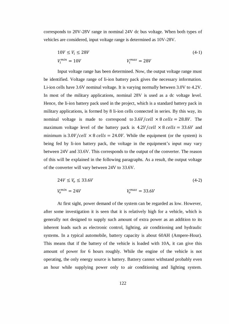
122
corresponds to 20V-28V range in nominal 24V dc bus voltage. When both types of
vehicles are considered, input voltage range is determined as 10V-28V.
(4-1)
Input voltage range has been determined. Now, the output voltage range must
be identified. Voltage range of li-ion battery pack gives the necessary information.
Li-ion cells have 3.6V nominal voltage. It is varying normally between 3.0V to 4.2V.
In most of the military applications, nominal 28V is used as a dc voltage level.
Hence, the li-ion battery pack used in the project, which is a standard battery pack in
military applications, is formed by 8 li-ion cells connected in series. By this way, its
nominal voltage is made to correspond to . The
maximum voltage level of the battery pack is and
minimum is . While the equipment (or the system) is
being fed by li-ion battery pack, the voltage in the equipment‟s input may vary
between 24V and 33.6V. This corresponds to the output of the converter. The reason
of this will be explained in the following paragraphs. As a result, the output voltage
of the converter will vary between 24V to 33.6V.
(4-2)
At first sight, power demand of the system can be regarded as low. However,
after some investigation it is seen that it is relatively high for a vehicle, which is
generally not designed to supply such amount of extra power as an addition to its
inherent loads such as electronic control, lighting, air conditioning and hydraulic
systems. In a typical automobile, battery capacity is about 60AH (Ampere-Hour).
This means that if the battery of the vehicle is loaded with 10A, it can give this
amount of power for 6 hours roughly. While the engine of the vehicle is not
operating, the only energy source is battery. Battery cannot withstand probably even
an hour while supplying power only to air conditioning and lighting system.

123
Especially in 12V dc bus voltage, even 60A –for 1 hour supply duration- corresponds
to a power of 720W. It means that the power consumption of a vehicle is about this
amount. As seen, energy source is very limited in this mode. Actually, vehicles are
designed to operate while its engine is active. While it is operating, an alternator
mechanically powered by the engine supplies all the electrical power needed by the
vehicle and charges the vehicle battery if power surplus exists at that instant. The
capacity of alternators also changes from vehicle to vehicle but its order is about 70A
for a typical automobile. This value is highly dependent on the rotational speed
(rev/min) of the engine and generally given at the maximum horse power rotational
speed, for example at 5000 rev/min. In other words, a moderate alternator can supply
at most 980W electrical power to the vehicle. This power will decrease to its %80
roughly due to the variation in engine rotational speed. As mentioned above and also
supported by the information gathered from the automobile producers, about 80% of
the alternator power is already consumed by the vehicle itself. The long and the short
of it, 400W-power demand of the equipment cannot be taken from the vehicle battery
-and thereby the alternator- even via direct battery connection. As a result, whereas
current carrying capability is a limiting factor in connection via cigarette lighter
adapter, power handling capability of alternator is a limitation in direct connection to
vehicle battery. At both connection modes, the converter will not meet the power
demand of the equipment alone. Hence, both of the power sources -namely the li-ion
battery pack and the converter- will be connected to the input of the equipment in
parallel. This is why the input voltage of the equipment is the same as the output
voltage of the converter. By the way, another important point should be highlighted.
The system does not always consume 400W. Rather, it has gradual power
consumption ranging from 25W to 400W. Therefore, it is highly possible that
although both of the sources are connected, only the converter can feed the system in
some situations. Note also that li-ion battery pack does not sink current in this mode
owing to its internal hardware, probably a reverse current diode or its equivalent in
terms of function. In order to make the converter the primary power source, control
method should be determined accordingly. In the other mode, again priority should
be given to the converter by the help of the control method. After all these
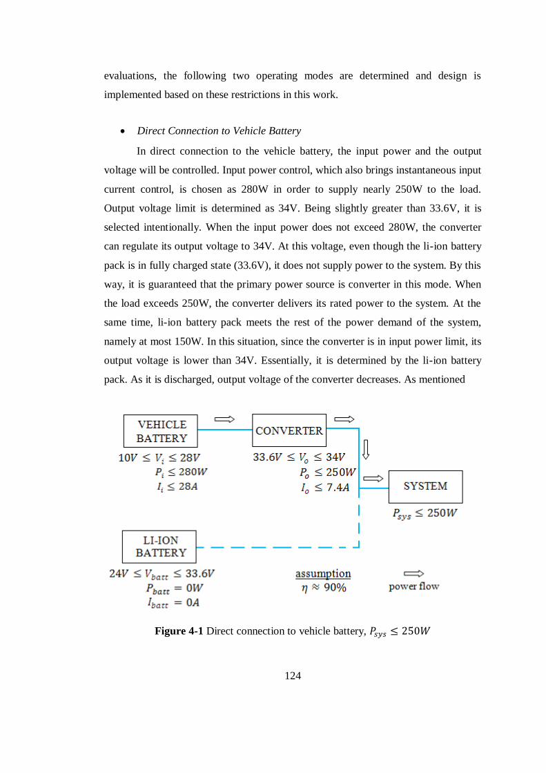
124
evaluations, the following two operating modes are determined and design is
implemented based on these restrictions in this work.
Direct Connection to Vehicle Battery
In direct connection to the vehicle battery, the input power and the output
voltage will be controlled. Input power control, which also brings instantaneous input
current control, is chosen as 280W in order to supply nearly 250W to the load.
Output voltage limit is determined as 34V. Being slightly greater than 33.6V, it is
selected intentionally. When the input power does not exceed 280W, the converter
can regulate its output voltage to 34V. At this voltage, even though the li-ion battery
pack is in fully charged state (33.6V), it does not supply power to the system. By this
way, it is guaranteed that the primary power source is converter in this mode. When
the load exceeds 250W, the converter delivers its rated power to the system. At the
same time, li-ion battery pack meets the rest of the power demand of the system,
namely at most 150W. In this situation, since the converter is in input power limit, its
output voltage is lower than 34V. Essentially, it is determined by the li-ion battery
pack. As it is discharged, output voltage of the converter decreases. As mentioned
Figure 4-1 Direct connection to vehicle battery,
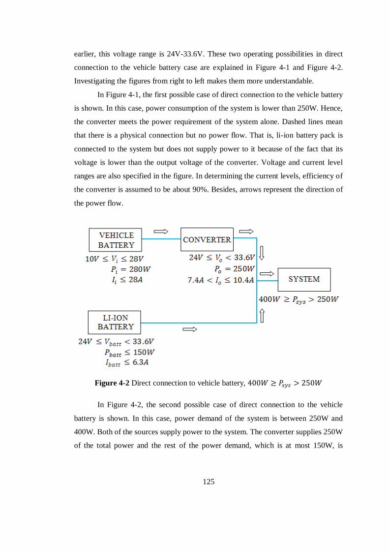
125
earlier, this voltage range is 24V-33.6V. These two operating possibilities in direct
connection to the vehicle battery case are explained in Figure 4-1 and Figure 4-2.
Investigating the figures from right to left makes them more understandable.
In Figure 4-1, the first possible case of direct connection to the vehicle battery
is shown. In this case, power consumption of the system is lower than 250W. Hence,
the converter meets the power requirement of the system alone. Dashed lines mean
that there is a physical connection but no power flow. That is, li-ion battery pack is
connected to the system but does not supply power to it because of the fact that its
voltage is lower than the output voltage of the converter. Voltage and current level
ranges are also specified in the figure. In determining the current levels, efficiency of
the converter is assumed to be about 90%. Besides, arrows represent the direction of
the power flow.
Figure 4-2 Direct connection to vehicle battery,
In Figure 4-2, the second possible case of direct connection to the vehicle
battery is shown. In this case, power demand of the system is between 250W and
400W. Both of the sources supply power to the system. The converter supplies 250W
of the total power and the rest of the power demand, which is at most 150W, is
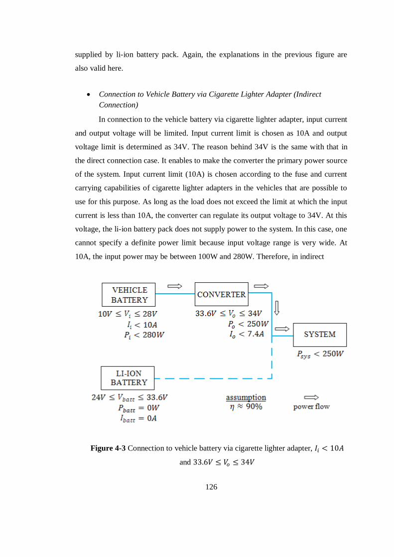
126
supplied by li-ion battery pack. Again, the explanations in the previous figure are
also valid here.
Connection to Vehicle Battery via Cigarette Lighter Adapter (Indirect
Connection)
In connection to the vehicle battery via cigarette lighter adapter, input current
and output voltage will be limited. Input current limit is chosen as 10A and output
voltage limit is determined as 34V. The reason behind 34V is the same with that in
the direct connection case. It enables to make the converter the primary power source
of the system. Input current limit (10A) is chosen according to the fuse and current
carrying capabilities of cigarette lighter adapters in the vehicles that are possible to
use for this purpose. As long as the load does not exceed the limit at which the input
current is less than 10A, the converter can regulate its output voltage to 34V. At this
voltage, the li-ion battery pack does not supply power to the system. In this case, one
cannot specify a definite power limit because input voltage range is very wide. At
10A, the input power may be between 100W and 280W. Therefore, in indirect
Figure 4-3 Connection to vehicle battery via cigarette lighter adapter,
and
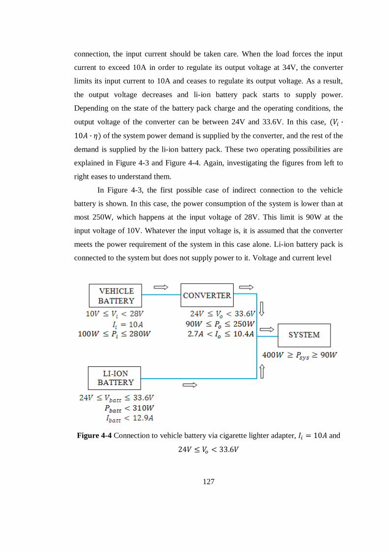
127
connection, the input current should be taken care. When the load forces the input
current to exceed 10A in order to regulate its output voltage at 34V, the converter
limits its input current to 10A and ceases to regulate its output voltage. As a result,
the output voltage decreases and li-ion battery pack starts to supply power.
Depending on the state of the battery pack charge and the operating conditions, the
output voltage of the converter can be between 24V and 33.6V. In this case,
of the system power demand is supplied by the converter, and the rest of the
demand is supplied by the li-ion battery pack. These two operating possibilities are
explained in Figure 4-3 and Figure 4-4. Again, investigating the figures from left to
right eases to understand them.
In Figure 4-3, the first possible case of indirect connection to the vehicle
battery is shown. In this case, the power consumption of the system is lower than at
most 250W, which happens at the input voltage of 28V. This limit is 90W at the
input voltage of 10V. Whatever the input voltage is, it is assumed that the converter
meets the power requirement of the system in this case alone. Li-ion battery pack is
connected to the system but does not supply power to it. Voltage and current level
Figure 4-4 Connection to vehicle battery via cigarette lighter adapter, and

128
ranges are also specified in the figure by the efficiency assumption of about 90%.
In Figure 4-4, the second possible case of indirect connection to the vehicle
battery is shown. In this case, power demand of the system is between 90W and
400W. Both of the sources supply power to the system. The converter supplies at
least 90W (at ) and at most 250W (at ) of the total power, and the
rest of the demand, which is at most 310W (at ) and 150W (at ), is
supplied by li-ion battery pack.
Possible operational conditions are defined so far. Based on them, the
following results are obtained in terms of the converter properties.
Input voltage range of the converter is 10-28V, and output voltage range is
24V-34V. It means that the converter is required not only to step-up but also
to step-down the input voltage. Šuk dc-to-dc converter, which is one of the
buck-boost converter types, is chosen for this purpose.
The converter should be designed to supply 250W maximum within the input
and output voltage ranges mentioned in (4-1) and (4-2).
Especially in controlling the input current, instead of its instantaneous or peak
value, its mean value will be controlled. However, in basic Šuk converter,
input current has such a waveform that it has a dc level and a triangular ac
component (ripple) superimposed on it. An example to this kind of a
waveform is shown in Figure 4-5. In this example, peak-to-peak ripple of
Figure 4-5 Input current waveform of a basic Šuk converter with 40% peak-to-
peak ripple

129
40% of the mean input current is selected typically just for illustration
purpose. As understood from Figure 4-5 easily, the instantaneous value of the
input current exceeds the current limit value in reality. In this situation, if the
current protection mechanism of the cigarette lighter adapter is a fast acting
one, it may be triggered by this type of current waveform. Even if the
mechanism is a slow acting one, for example a fuse, this type of a waveform
may have an adverse effect on it. Fuses normally have quite small internal
resistances and they are heated up and become open by the heat caused by the
RMS value of the current passing through them. As the ac component of the
current waveform increases while its dc level is kept constant, its RMS value
increases as well. For example, the waveform seen in Figure 4-5 has a mean
value of 10A but RMS value greater than 10A. In this situation, fuse may be
triggered as well due to the unwanted feature of the current waveform. In
buck-boost converter topology, this situation is worse because it has pulsating
input current waveform. Hence, Šuk converter seems as a better solution.
Moreover, coupled-inductor Šuk converter with ripple-free input current
version seems to be the best solution. As a result, CIŠC with ripple-free input
current version is decided to design in this work.
The converter is required to conduct different control strategies in direct and
indirect connections to the vehicle battery. They are mentioned in the
succeeding pages. Therefore, there must be a way for the converter to
understand which control strategy to implement at that operation. When it is
investigated, it is seen that this cannot be done automatically, for example by
sampling the input and output voltages. Only an operator can determine the
control strategy by looking at the connection type, direct or indirect. Hence, a
manual switch will be added to the converter. It will have two positions.
According to the position of it, the converter will run the corresponding
control strategy.

130
As mentioned earlier, in direct connection to the vehicle battery, output
voltage and input power will be controlled. In order to do this, feedbacks will
be taken from output voltage and input current. Most of the time, the system
is expected to consume its rated power of 400W; therefore, the converter will
be performing input power control. It will rarely control the output voltage.
Hence, this control mode is called ‘constant input power mode’ in this work.
In indirect connection to the vehicle battery, output voltage and input current
will be controlled. In this control mode, again, input current and output
voltage will be taken as feedbacks. Similar to the direct connection case, the
converter will control the input current most of the time. Therefore, this
control mode is called ‘constant input current mode’.
At this point, selection and design of the circuit components can be
performed.
4.3 SELECTION AND DESIGN OF THE CIRCUIT
COMPONENTS
In this section; selection of the switch, diode, energy transferring capacitor
( ) and output capacitor ( ) will be detailed and based on the technical
requirements. Then, the coupled-inductor providing ripple-free input current will be
designed.
4.3.1 Selection of MOSFET
First of all, why MOSFET is selected may be required to explain. As
mentioned earlier, the switching frequency is determined as 100 kHz. When it is
searched, it is seen that 100kHz is reasonable at this power rating.[5
] When the
operating voltage levels, current levels and the switching frequency are taken into
consideration, MOSFET is seen as the most suitable switch. Another possibility is
IGBT, but it is more suitable at lower frequencies and higher voltage/higher current

131
applications. When the switch market is searched, even for the most suitable IGBT
for this application, total loss (conduction loss and switching loss) turns out to be
higher than that of a moderate MOSFET. Hence, after a short market search,
MOSFET is determined as the switch.
Now, to which voltage and current stresses the selected switch must
withstand will be determined. Then, based on this information, a suitable switch will
be selected according to its total loss. Necessary data needed in selection of the
switch is given in Table 4-1. The maximum voltage, current and power dissipation
stresses occur at „end operating points‟, at which the voltage levels are at their
maximum or minimum. Hence, these operating points are considered throughout the
selection and design of the circuit components. There are four end operating points.
First End Operating Point: 10V and 24V
Second End Operating Point: 10V and 34V
Third End Operating Point: 28V and 24V
Fourth End Operating Point: 28V and 34V
The efficiency of the coupled-inductor Šuk converter, CIŠM is assumed to be
90% in the preparation of Table 4-1. One may refer to the circuit schematic of CIŠM
with parasitic elements in Figure 3-16 for the labels in the tables of this section. The
instantaneous values, with small letters, are shown in that figure. In the tables,
however, steady-state (or mean) values, with capital letters, are used; because it
makes more sense. Similarly, mean value of the duty-factor, is used in the tables.
, and labels are new. When the switch or the diode is on, it carries the
sum of and
, which corresponds to the sum of input and output currents. This
value is labeled by . When the switch or the diode is off, it blocks , which is
the sum of input and output voltages. This value is labeled by . is the RMS
current of the switch. It will be used in power loss calculation.

132
Table 4-1 Voltage and current stresses on the switch
10 27,8 24 10,4 0,706 0,294 34 38,2 32,1
10 27,8 34 7,4 0,773 0,227 44 35,1 30,9
28 9,9 24 10,4 0,462 0,538 52 20,3 13,8
28 9,9 34 7,4 0,548 0,452 62 17,3 12,8
As inferred from Table 4-1, the selected switch has to withstand 62V during
time interval, where is the switching frequency. However, the voltage
rating of the selected MOSET should be higher than this because of the voltage
overshoots during transient period. Note also that voltage is not pure dc, however
its voltage ripple is around 1-2% of its mean voltage and considered as negligible.
This topic will be elaborated in selection section. In terms of current rating, it is
seen that the switch carries at most 38.2A during time interval. Again, there is a
ripple current on inductor but it is at negligible level. 62V and 38.2A values can
be regarded as the continuous operating conditions, because they are applied to the
switch for relatively long time periods compared to the transient periods and they are
periodic waveforms. As a result, the switch should be selected using this data.
will be used in conduction loss calculation for the switch. This value is
simply obtained by „root mean square‟ definition.
(4-3)
where is the switching period. The switch carries current during time interval
only. Hence, when this simplification is applied to (4-3), it yields;
(4-4)
Hence, the maximum RMS current which can be carried by the switch is given as;

133
Then, the conduction loss in the switch can be calculated by;
(4-5)
As it is seen, even 10mΩ , which can be considered as a low resistance for a
typical MOSFET at these ratings, causes 10.3W conduction loss. Since RMS value
of the current is relatively high, a MOSFET with lower will be more suitable for
the application; otherwise at least two switches will be paralleled.
Another important point in determining the suitable switch is the switching
loss. The switching loss on the switch can be expressed as [2
];
(4-6)
Hence, in order to keep low, rise and fall times should be low for the switch
selected for use. Consequently, MOSFET with the lowest total power dissipation
among the available MOSFETs is chosen as the following one;
Company: Infineon Part Number: IPP045N10N3 G
Continuous Continuous
Note that:
and
Thus, the conduction and the switching power losses at end operating points
for the switch are calculated and tabulated as Table 4-2.
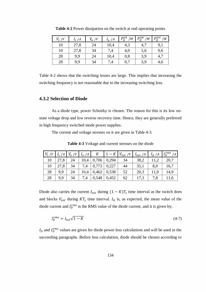
134
Table 4-2 Power dissipation on the switch at end operating points
10 27,8 24 10,4 4,3 4,7 9,1
10 27,8 34 7,4 4,0 5,6 9,6
28 9,9 24 10,4 0,8 3,9 4,7
28 9,9 34 7,4 0,7 3,9 4,6
Table 4-2 shows that the switching losses are large. This implies that increasing the
switching frequency is not reasonable due to the increasing switching loss.
4.3.2 Selection of Diode
As a diode type, power Schottky is chosen. The reason for this is its low on-
state voltage drop and low reverse recovery time. Hence, they are generally preferred
in high frequency switched mode power supplies.
The current and voltage stresses on it are given in Table 4-3.
Table 4-3 Voltage and current stresses on the diode
10 27,8 24 10,4 0,706 0,294 34 38,2 11,2 20,7
10 27,8 34 7,4 0,773 0,227 44 35,1 8,0 16,7
28 9,9 24 10,4 0,462 0,538 52 20,3 11,0 14,9
28 9,9 34 7,4 0,548 0,452 62 17,3 7,8 11,6
Diode also carries the current during time interval as the switch does
and blocks during time interval. is, as expected, the mean value of the
diode current and is the RMS value of the diode current, and it is given by;
(4-7)
and values are given for diode power loss calculations and will be used in the
succeeding paragraphs. Before loss calculation, diode should be chosen according to

135
voltage and current stresses. As understood from Table 4-3, selected diode has to
withstand 38.2A and 62V. As a consequence, the following diode is chosen.
Company: ST Microelectronics Part Number: STPS80170C
Note that:
Actually, using 38.2A as a mean value is not exactly true. However, in many of the
diode datasheets, there is no detailed information about allowable peak repetitive
forward current. Therefore, 38.2A is used as the mean value to be on the safe side.
In the datasheet of this diode, the following equation is given for use in the
conduction loss calculation as;
(4-8)
From which, the following relationship is established;
(4-9)
It is clearly seen that and must be as small as possible in order to have low
power dissipation on the diode. This was the driving force in diode selection. In
diodes, reverse recovery phenomenon causes switching loss. However, there is not
any data about this issue in most of the diode datasheets. Especially in fast switching
ones, no information related to reverse recovery loss is found. This loss may be
negligible with respect to conduction loss. As a result, reverse recovery loss is
neglected in this work.
Conduction losses of the diode at end operating points are given in Table 4-4.

136
Table 4-4 Power dissipation on the diode at end operating points
10 27,8 24 10,4 8,3
10 27,8 34 7,4 5,8
28 9,9 24 10,4 7,5
28 9,9 34 7,4 5,2
To sum up, power dissipation on the diode seems to be reasonable.
4.3.3 Selection of
holds mean voltage. There is a voltage ripple on it at the switching
frequency. The amplitude of the ripple voltage will be determined by the selection of
the capacitor. In terms of current stress, is charged by during and
discharged by during . That is to say, current stress on is severe. In
order to see the effect of current stress, simple capacitor model should be
investigated.
Figure 4-6 Simple capacitor model
As seen in Figure 4-6 and Figure 3-16, a capacitor has an equivalent series
resistance, ESR. This resistance has two important effects. First, the RMS current
passing through the capacitor causes power dissipation on the capacitor, which
results in heating of itself. The amount of power dissipation can be calculated in the

137
following and known manner. Note that although the mean value of the capacitor
current is zero at steady-state, its RMS value can be very large.
(4-10)
The second important effect of ESR is related to voltage ripple on the capacitor. As
mentioned earlier, capacitors have zero mean but nonzero RMS current values at
steady-state operation. It means that , in Figure 4-6, changes direction periodically.
This change of direction leads to extra voltage ripple and this ripple is just because of
ESR. Generally, only the following ripple source is considered: Increase or decrease
of capacitor charge results in production of some ripple on the capacitor voltage.
Referring to Figure 4-6;
(4-11)
Note that is used instead of
in (4-11) because the voltage that cannot
change instantaneously is . Contrary to
, may change instantly when
the magnitude or direction of changes. can be expressed as;
(4-12)
In order to clarify the situation, let‟s consider that the circuit is transiting form
Mode 2 to Mode 1. In Mode 2, is the input current, which is constant at . At this
moment, (4-13) can be written, in which superscript means that those quantities
assume values equal to those resulting just before the switching instant.
(4-13)
In Mode 1, is
with small ripple and it can be considered as constant. As
mentioned earlier, mean value of is equal to . Therefore, (4-14) can be written
in Mode 1. Similarly, superscript means that those quantities assume values equal
to those resulting just after the switching instant.

138
(4-14)
Just before the switching, (4-13) is valid, but after the switching, (4-14) is valid. As a
known fact,
does not change instantly. Hence,
is equal to
.
However,
decreases instantly in this example. This fact is explained below step
by step. The term
represents the voltage change at the switching instant.
(4-15)
(4-16)
(4-17)
This sharp voltage change occurs at each switching instant. Whereas decreases
much in Mode 2 to Mode 1 transition, it increases the same amount in Mode
1 to Mode 2 transition. As an addition to this sharp change, capacitor voltage
changes because of the charge variation in it. Which kind of ripple will be more
severe depends on the amount of current stress, size of the capacitance and ESR of
the capacitor. These should be taken into account in the selection of the capacitors.
In capacitor selection, power dissipation is aimed to be at reasonable level
and not to cause overheating of it. Another restriction comes from the assumptions
made in CHAPTER 2. In those assumptions, voltage ripples on the capacitors are
neglected. Therefore, capacitor voltage ripples should be limited in this section.
When calculated, it has been observed that 2% peak-to-peak voltage ripple results in
a reasonable capacitor bank for . Furthermore, its voltage ripple is not as critical as
that of the output capacitor. Its voltage ripple must be limited just in order to be as
close as possible to constant capacitor voltage assumption. Consequently, 2% is a
suitable choice for the voltage ripple percent of .
When the available capacitors are searched, it is decided to use the following.
Company: Cubisic Part Number: A710160
Type: Aluminium Electrolytic
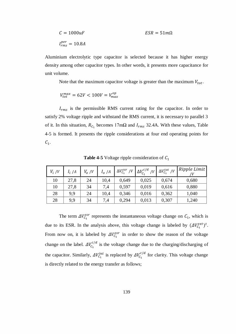
139
Aluminium electrolytic type capacitor is selected because it has higher energy
density among other capacitor types. In other words, it presents more capacitance for
unit volume.
Note that the maximum capacitor voltage is greater than the maximum .
is the permissible RMS current rating for the capacitor. In order to
satisfy 2% voltage ripple and withstand the RMS current, it is necessary to parallel 3
of it. In this situation, becomes 17mΩ and 32.4A. With these values, Table
4-5 is formed. It presents the ripple considerations at four end operating points for
.
Table 4-5 Voltage ripple consideration of
10 27,8 24 10,4 0,649 0,025 0,674 0,680
10 27,8 34 7,4 0,597 0,019 0,616 0,880
28 9,9 24 10,4 0,346 0,016 0,362 1,040
28 9,9 34 7,4 0,294 0,013 0,307 1,240
The term
represents the instantaneous voltage change on , which is
due to its ESR. In the analysis above, this voltage change is labeled by
.
From now on, it is labeled by
in order to show the reason of the voltage
change on the label.
is the voltage change due to the charging/discharging of
the capacitor. Similarly,
is replaced by
for clarity. This voltage change
is directly related to the energy transfer as follows;

140
(4-18)
(4-19)
(4-20)
As it can be understood from the derivation above,
represents the peak-to-
peak voltage ripple magnitude. Sum of
and
gives the total voltage
ripple on the capacitor, and it is named as
on the table. is 2% of
the voltage on the capacitor, . As seen in Table 4-5, the maximum voltage ripple
on the capacitor is less than the value at each end operating point. Also
note that over 95% of the ripple is caused by the ESR of the capacitor. Instead of the
selected capacitor, a capacitor bank with lower capacitance and ESR value might be
chosen. That capacitor type may be ceramic or tantalum, which have lower energy
density but lower ESR. In that situation, most of the ripple would be caused by
charging/discharging instead of ESR. Besides, smaller capacitance would probably
result in faster dynamic response at the expense of weaker stability. There is a trade-
off between them. As a pure advantage, power loss would be lower in that situation.
Since stability seems more important than the dynamic response in the project, the
selected capacitor is preferred.
In order to verify the ripple considerations above, simulation is conducted
with all parasitic components at one of the operating points: Full load, ,
. As seen in Figure 4-7, total ripple magnitude (671mV) is very close to the
calculated one (674mV). There is a sharp change in the capacitor voltage, whose
magnitude is as expected. Lines with lower slopes at the bottom and top are where
the capacitor is being either charged or discharged. There is a small amplitude
difference between them. It is due to the fact that is not pure dc contrary to the
prior assumption made. Due to the small current ripple on it, small amplitude
difference is observed.
141
Figure 4-7 waveform for voltage ripple consideration, full load, ,
RMS current and power dissipation with the selected capacitor at each end
operating points are given in Table 4-6.
Table 4-6 Power dissipation on at end operating points
10 27,8 24 10,4 0,706 0,294 17,4 5,2 1,7
10 27,8 34 7,4 0,773 0,227 14,7 3,7 1,2
28 9,9 24 10,4 0,462 0,538 10,2 1,8 0,6
28 9,9 34 7,4 0,548 0,452 8,6 1,3 0,4
is calculated by using the RMS definition in (4-3), as;
(4-21)
Note that the maximum RMS ripple current is less than the maximum
allowable RMS current of the capacitor bank.

142
term represents the total power dissipation on 3 capacitors and
each of
them. As it is seen in Table 4-6, capacitors have moderate power dissipations.
4.3.4 Selection of
holds the mean output voltage, . Again, there is a voltage ripple on it at
the switching frequency and its amplitude will be determined by . That is, ripple
voltage consideration of resembles to that of . However, their current
waveforms are highly different. The current waveform of is dictated by the input
and output inductors. Nevertheless, for , the current waveform is determined by
the output inductor current and the output current. (4-22) can be written by referring
to Figure 3-16.
(4-22)
The difference current between and is supplied by . Since the integral of it
has to be zero at steady-state, both sinks and supplies current within a period. This
fact can be clarified by the help of Figure 4-8. Let‟s assume that the load sinks pure
Figure 4-8 Current consideration of , a) waveform, b) waveform, c)
waveform
143
dc current. In this situation, the waveforms shown in Figure 4-8 are observed. As
seen clearly, has not severe current stress. It meets the current unbalance between
the output current and the output inductor current. Hence, it may be called output
filter capacitor. In order to determine the voltage ripple on , some derivations are
needed. Firstly, the ripple magnitude that is caused by ESR of the capacitor must be
derived. As it is seen in Figure 4-8, peak-to-peak current change is . Hence,
(4-23) can be written easily. Contrary to the ripple behavior in case, this voltage
ripple does not change abruptly because current does not do so. Rather, it resembles
to the ripple voltage due to charging or discharging of the capacitor.
(4-23)
The term
represents the peak-to-peak magnitude of the part of the voltage
ripple caused only by ESR. Second part of the voltage ripple is labeled by
and
it is caused by charging and discharging of the capacitor. In order to find a
relationship between
and operating point parameters, Figure 4-9 can be
helpful.
Figure 4-9 waveform for voltage ripple consideration due to
charging/discharging
is charged during and discharged during successive . Hence, its voltage
increases shaded much. Following equations can be written for the case;

144
(4-24)
(4-25)
(4-26)
(4-27)
(4-28)
Similar derivation of (4-28) can also be found in [2]. This derivation is given
intentionally in order to show the difference between and in terms of voltage
ripple consideration.
(4-23) and (4-28) are ready to use in determining the output capacitance.
Before it, a simple modification may result in a better solution. 2% voltage ripple
restriction for case seems a little bit looser for the output voltage. voltage is
inside the circuit contrary to voltage, which is the output of the circuit. Hence, a
stricter condition may be desired at this point. As a result, the ripple requirement on
the output capacitor voltage is selected as 1%.
After some investigation, it is seen that using two of the following capacitor
meets the voltage ripple requirement and cause a reasonable power loss.
Company: AVX Corporation Part Number: 12105C475K4Z2A
Type: Ceramic Capacitor
It is a surface mount ceramic capacitor. Since the current stress is very light and the
transferred energy is very small, the required capacitance turns out to be low. This
justifies using ceramic capacitor. Its ESR and
being not given in its datasheet,
they are taken from the datasheets of equivalent products. By paralleling two of it,
the following values are obtained.
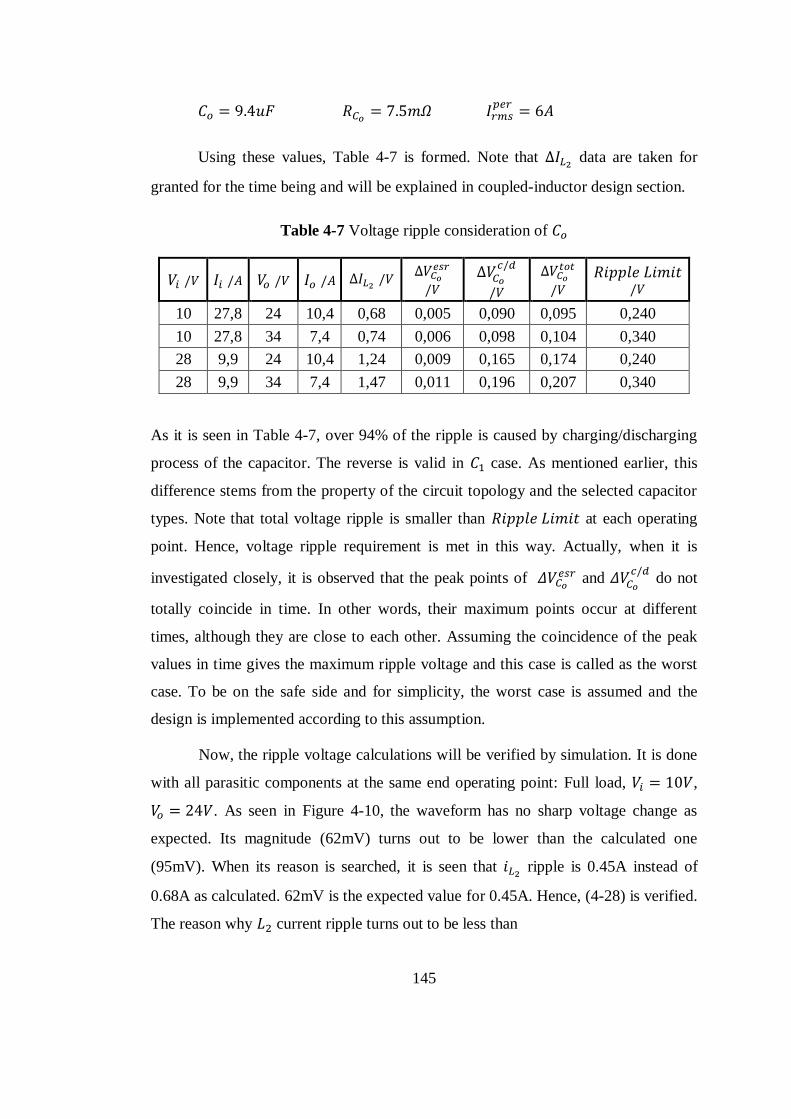
145
Using these values, Table 4-7 is formed. Note that data are taken for
granted for the time being and will be explained in coupled-inductor design section.
Table 4-7 Voltage ripple consideration of
10 27,8 24 10,4 0,68 0,005 0,090 0,095 0,240
10 27,8 34 7,4 0,74 0,006 0,098 0,104 0,340
28 9,9 24 10,4 1,24 0,009 0,165 0,174 0,240
28 9,9 34 7,4 1,47 0,011 0,196 0,207 0,340
As it is seen in Table 4-7, over 94% of the ripple is caused by charging/discharging
process of the capacitor. The reverse is valid in case. As mentioned earlier, this
difference stems from the property of the circuit topology and the selected capacitor
types. Note that total voltage ripple is smaller than at each operating
point. Hence, voltage ripple requirement is met in this way. Actually, when it is
investigated closely, it is observed that the peak points of
and
do not
totally coincide in time. In other words, their maximum points occur at different
times, although they are close to each other. Assuming the coincidence of the peak
values in time gives the maximum ripple voltage and this case is called as the worst
case. To be on the safe side and for simplicity, the worst case is assumed and the
design is implemented according to this assumption.
Now, the ripple voltage calculations will be verified by simulation. It is done
with all parasitic components at the same end operating point: Full load, ,
. As seen in Figure 4-10, the waveform has no sharp voltage change as
expected. Its magnitude (62mV) turns out to be lower than the calculated one
(95mV). When its reason is searched, it is seen that ripple is 0.45A instead of
0.68A as calculated. 62mV is the expected value for 0.45A. Hence, (4-28) is verified.
The reason why current ripple turns out to be less than
146
Figure 4-10 waveform for voltage ripple consideration, full load, ,
Calculated value is explained in Figure 2-22 and commented.
Now, let‟s look at the power loss on . When the RMS current definition in
(4-3) is applied to the waveform shown in Figure 4-9, the following equality can be
derived.
(4-29)
By utilizing this equality, power dissipation on the output capacitor is presented in
Table 4-8. As seen in this table, total power loss on the output capacitor bank is in
1mW order. Hence, it is neglected.
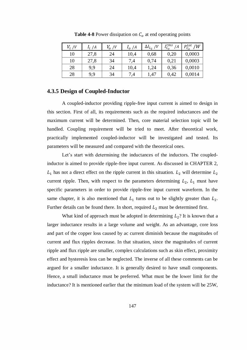
147
Table 4-8 Power dissipation on at end operating points
10 27,8 24 10,4 0,68 0,20 0,0003
10 27,8 34 7,4 0,74 0,21 0,0003
28 9,9 24 10,4 1,24 0,36 0,0010
28 9,9 34 7,4 1,47 0,42 0,0014
4.3.5 Design of Coupled-Inductor
A coupled-inductor providing ripple-free input current is aimed to design in
this section. First of all, its requirements such as the required inductances and the
maximum current will be determined. Then, core material selection topic will be
handled. Coupling requirement will be tried to meet. After theoretical work,
practically implemented coupled-inductor will be investigated and tested. Its
parameters will be measured and compared with the theoretical ones.
Let‟s start with determining the inductances of the inductors. The coupled-
inductor is aimed to provide ripple-free input current. As discussed in CHAPTER 2,
has not a direct effect on the ripple current in this situation. will determine
current ripple. Then, with respect to the parameters determining , must have
specific parameters in order to provide ripple-free input current waveform. In the
same chapter, it is also mentioned that turns out to be slightly greater than .
Further details can be found there. In short, required must be determined first.
What kind of approach must be adopted in determining ? It is known that a
larger inductance results in a large volume and weight. As an advantage, core loss
and part of the copper loss caused by ac current diminish because the magnitudes of
current and flux ripples decrease. In that situation, since the magnitudes of current
ripple and flux ripple are smaller, complex calculations such as skin effect, proximity
effect and hysteresis loss can be neglected. The inverse of all these comments can be
argued for a smaller inductance. It is generally desired to have small components.
Hence, a small inductance must be preferred. What must be the lower limit for the
inductance? It is mentioned earlier that the minimum load of the system will be 25W,
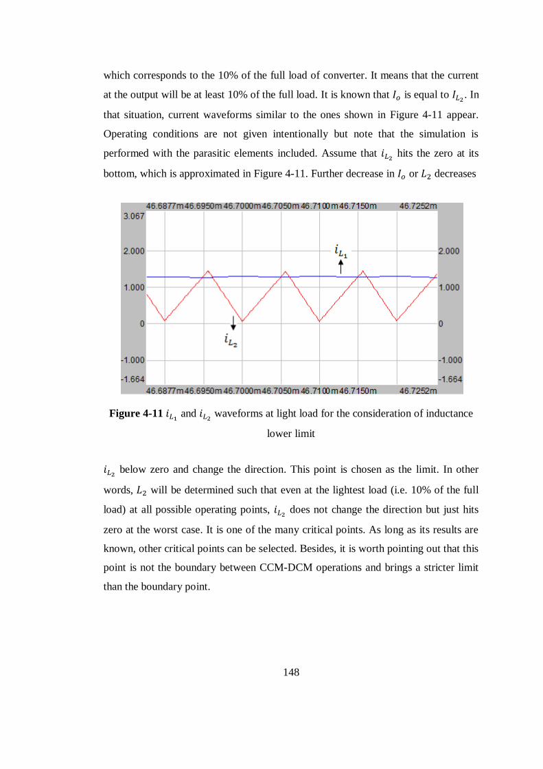
148
which corresponds to the 10% of the full load of converter. It means that the current
at the output will be at least 10% of the full load. It is known that is equal to . In
that situation, current waveforms similar to the ones shown in Figure 4-11 appear.
Operating conditions are not given intentionally but note that the simulation is
performed with the parasitic elements included. Assume that hits the zero at its
bottom, which is approximated in Figure 4-11. Further decrease in or decreases
Figure 4-11 and
waveforms at light load for the consideration of inductance
lower limit
below zero and change the direction. This point is chosen as the limit. In other
words, will be determined such that even at the lightest load (i.e. 10% of the full
load) at all possible operating points, does not change the direction but just hits
zero at the worst case. It is one of the many critical points. As long as its results are
known, other critical points can be selected. Besides, it is worth pointing out that this
point is not the boundary between CCM-DCM operations and brings a stricter limit
than the boundary point.
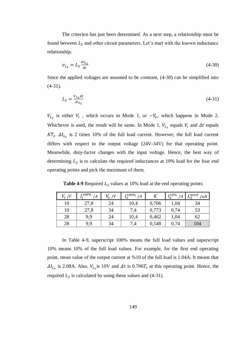
149
The criterion has just been determined. As a next step, a relationship must be
found between and other circuit parameters. Let‟s start with the known inductance
relationship.
(4-30)
Since the applied voltages are assumed to be constant, (4-30) can be simplified into
(4-31).
(4-31)
is either , which occurs in Mode 1, or , which happens in Mode 2.
Whichever is used, the result will be same. In Mode 1, equals and equals
. is 2 times 10% of the full load current. However, the full load current
differs with respect to the output voltage (24V-34V) for that operating point.
Meanwhile, duty-factor changes with the input voltage. Hence, the best way of
determining is to calculate the required inductances at 10% load for the four end
operating points and pick the maximum of them.
Table 4-9 Required values at 10% load at the end operating points
10 27,8 24 10,4 0,706 1,04 34
10 27,8 34 7,4 0,773 0,74 53
28 9,9 24 10,4 0,462 1,04 62
28 9,9 34 7,4 0,548 0,74 104
In Table 4-9, superscript 100% means the full load values and superscript
10% means 10% of the full load values. For example, for the first end operating
point, mean value of the output current at %10 of the full load is 1.04A. It means that
is 2.08A. Also,
is 10V and is 0.706 at this operating point. Hence, the
required is calculated by using these values and (4-31).
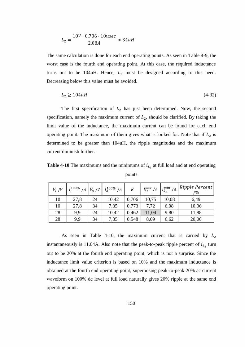
150
The same calculation is done for each end operating points. As seen in Table 4-9, the
worst case is the fourth end operating point. At this case, the required inductance
turns out to be 104uH. Hence, must be designed according to this need.
Decreasing below this value must be avoided.
(4-32)
The first specification of has just been determined. Now, the second
specification, namely the maximum current of , should be clarified. By taking the
limit value of the inductance, the maximum current can be found for each end
operating point. The maximum of them gives what is looked for. Note that if is
determined to be greater than 104uH, the ripple magnitudes and the maximum
current diminish further.
Table 4-10 The maximums and the minimums of at full load and at end operating
points
10 27,8 24 10,42 0,706 10,75 10,08 6,49
10 27,8 34 7,35 0,773 7,72 6,98 10,06
28 9,9 24 10,42 0,462 11,04 9,80 11,88
28 9,9 34 7,35 0,548 8,09 6,62 20,00
As seen in Table 4-10, the maximum current that is carried by
instantaneously is 11.04A. Also note that the peak-to-peak ripple percent of turn
out to be 20% at the fourth end operating point, which is not a surprise. Since the
inductance limit value criterion is based on 10% and the maximum inductance is
obtained at the fourth end operating point, superposing peak-to-peak 20% ac current
waveform on 100% dc level at full load naturally gives 20% ripple at the same end
operating point.
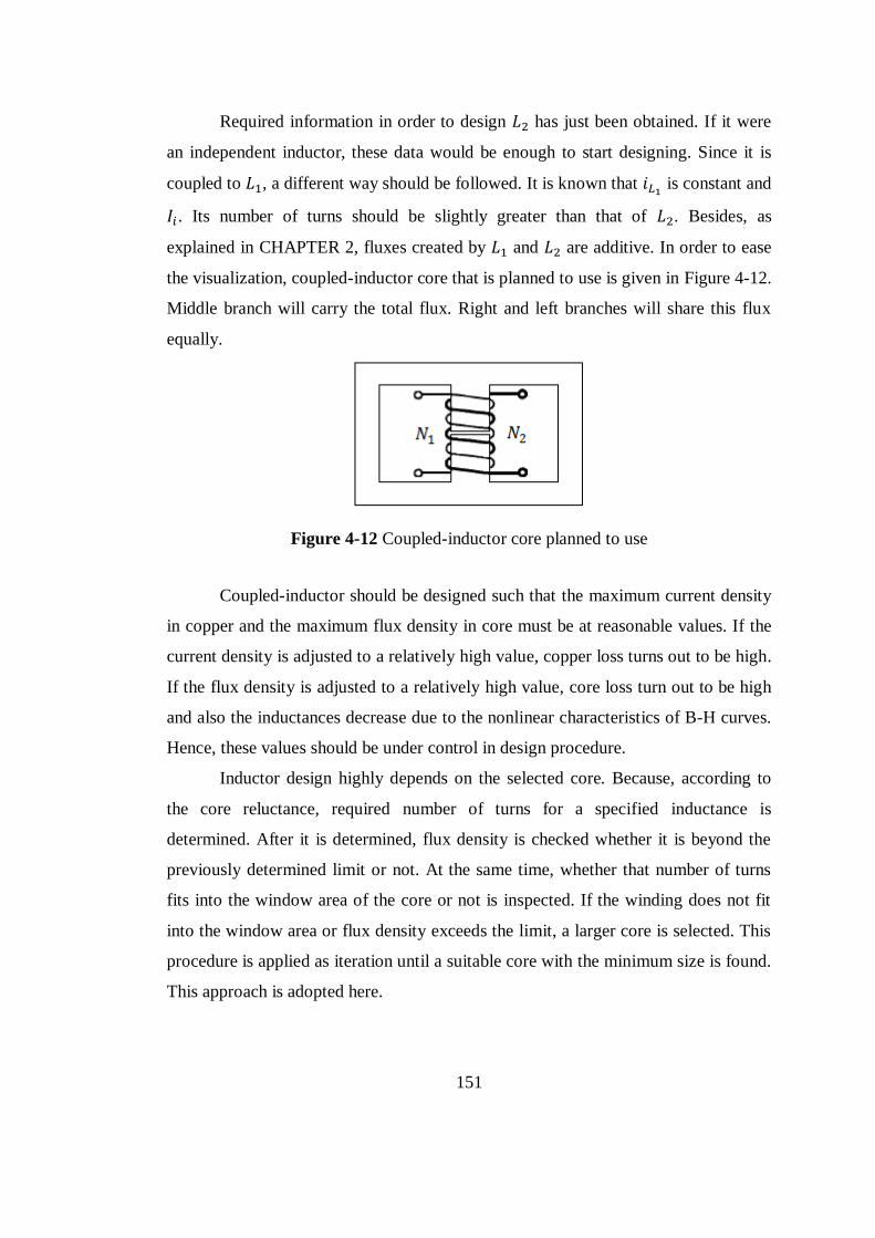
151
Required information in order to design has just been obtained. If it were
an independent inductor, these data would be enough to start designing. Since it is
coupled to , a different way should be followed. It is known that is constant and
. Its number of turns should be slightly greater than that of . Besides, as
explained in CHAPTER 2, fluxes created by and are additive. In order to ease
the visualization, coupled-inductor core that is planned to use is given in Figure 4-12.
Middle branch will carry the total flux. Right and left branches will share this flux
equally.
Figure 4-12 Coupled-inductor core planned to use
Coupled-inductor should be designed such that the maximum current density
in copper and the maximum flux density in core must be at reasonable values. If the
current density is adjusted to a relatively high value, copper loss turns out to be high.
If the flux density is adjusted to a relatively high value, core loss turn out to be high
and also the inductances decrease due to the nonlinear characteristics of B-H curves.
Hence, these values should be under control in design procedure.
Inductor design highly depends on the selected core. Because, according to
the core reluctance, required number of turns for a specified inductance is
determined. After it is determined, flux density is checked whether it is beyond the
previously determined limit or not. At the same time, whether that number of turns
fits into the window area of the core or not is inspected. If the winding does not fit
into the window area or flux density exceeds the limit, a larger core is selected. This
procedure is applied as iteration until a suitable core with the minimum size is found.
This approach is adopted here.

152
The design will be explained by the help of the following four tables; namely
Table 4-11, Table 4-12, Table 4-13 and Table 4-14. These tables are correlated with
each other. Because of this correlation and abundance of the parameters, iterations
are implemented in a Microsoft Excel sheet. These tables are the snapshots of the
result of the iteration. In other words, they belong to the ultimately selected core and
windings.
Let‟s start with Table 4-11. As it is expected, the maximum current and flux
densities occur at the maximum input and output current cases. When Table 4-10 is
investigated, it is seen that the maximum of the sum of and
occurs at the
first end operating point. Hence, these values are written in Table 4-11. Required
value (104.4uH) is another input. Diameter of the selected wire is 0.55mm. Instead of
using single but thick wire, multiple of thin wire is preferred. Thin wire is generally
used where ac current amplitude and switching frequency are high. In this way, skin
effect is considered and thin wire is used in order to decrease the ac resistance of the
wire. In this problem, is always constant and
has at most 20% peak-to-peak
ripple current at full load. Hence, even if the ac resistance of inductor were
designed high, its loss would be low because ac current magnitude is very low. Still,
skin depth may be checked. Its known formulation is given in (4-33).
(4-33)
Skin depth is calculated as:
Skin depth is defined as the distance from the surface to the inner of the conductor
where current density is ( ) of the surface current density. In a wire with
0.55mm diameter, depth of the innermost point is 0.275mm, which is close to the
calculated skin depth. In short, this wire is selected such that ac losses on the
windings can be neglected.

153
Let‟s continue with the other parameters in Table 4-11. Cross section area of
a single wire is simply calculated as . Then, current
density limit must be set in order calculate how many wire must be paralleled in
order to carry that much of input and output currents. When many examples are
investigated, it is seen that most of them are in the range of 2A/mm2 to 6A/mm
2.
Midpoint of them, 4A/mm2, is selected and checked whether it is reasonable or not.
In this situation, it is observed that windings have moderate series resistances and
power dissipations, which will be presented in the following paragraphs. Of course,
selecting a current density below 4A/mm2 would be better, but in 4A/mm
2 case
windings just about fit into the coil former, to which the windings are wound. Hence,
4A/mm2 is evaluated as a satisfactory value. Using this information, required total
cross section area for is calculated as:
How many wires can provide this total cross section area is found as the ceiling value
of . By the way, due to the rounding of the numbers in the
snapshots of the tables, some unimportant inconsistencies in the values of the
parameters may be observed. They exist only in the snapshots and accumulative error
is eliminated by use of Excel sheet, which keeps the numbers at large amount of
decimal points. To sum up, it is obtained that 30 wires should be paralleled for
and 12 wires for . In that situation, current densities are set to just below 4A/mm2
for both inductors.
At this step, whether the windings can fit into the selected coil former or not
will be investigated. For , net occupied area for 1 turn of 30 wires is calculated as:
Number of turns is required now. This value comes from Table 4-14. As mentioned
earlier, the design procedure is iterative and the tables are correlated. Determination
of number of turns will be explained later. Let‟s take it for granted for the time being.
Then, the net occupied area by 19.5 turns of 30 wires is calculated as:

154
In Table 4-11, gross values are given. Net area is named as the area of circle,
whereas gross area is considered as the area of the square which includes that circle.
There is a correction factor of 4/π between the areas. As it is known, there exist areas
between the circles which are not utilized. In order to asses more accurately, this
correction is performed at this stage. As a result, gross occupied area of winding is
calculated as:
Similarly, gross occupied area of winding is calculated as 66mm2. Total of them is
found as 243mm2. Window area of the selected coil former is 462mm
2. At first sight
it is seen that only 53% of the area is utilized. However, when practical winding
issues are considered, this utilization factor seems to be reasonable. When the
windings were wound, it has been observed that window utilization factor could be
increased to at most 60%. However, it has been left as it is.
Table 4-11 Wire and window area considerations in coupled-inductor design
constant and maximum 27,78
maximum 10,75
104,4
0,55
0,24
4
6,94
30
2,76
12
177
66
243
462
Let‟s go on with Table 4-12. In this table, some parameters of the selected
core are given. Before it, the identification of the core is presented as;

155
Company: Epcos Part Number: PM 74/59
Material: Ferrite N27 Air gap: 3.8mm
First of all, why gapped ferrite core is chosen can be explained briefly. As it is
known, there is a trade-off between high and low hysteresis loss in core material
types. Ferrite materials have the lowest and hysteresis loss values; laminations
have the highest and hysteresis loss values; and powdered cores are between
them. At , generally ferrite material is preferred for filter inductors.[5
]
By doing so, hysteresis loss is desired to keep at a low level; because filter inductors
generally have relatively high flux swing. However, in this work, flux swing is
relatively low: is always constant and
has relatively low current ripple. By
grounding on this fact, it would be argued that ferrite is not necessarily the optimum
selection. For example, with its moderate hysteresis loss, powdered core would be
selected. In that situation, it would provide smaller size and its hysteresis loss would
be reasonable by the help of the low flux swing in the coupled-inductor. These
arguments may be true; however, there is a special situation of the coupled-inductor.
As mentioned in CHAPTER 2, there must be relationship between leakage and
magnetizing inductances of and for complete ripple cancellation in . As a
known fact, inductance of an inductor decreases little or much as the current
increases. In other words, reluctance of an inductor increases with increasing flux
density. Characteristic of this change differs from material to material. This fact is
observed in B-H curves. For example, air has a linear B-H curve, its slope is very
low and magnetic saturation is not observed. B-H curves of ungapped ferrite
materials are comprised of two „almost‟ linear portions. First portion represents the
magnetic permeability of ferrite material and its slope is very high. Once value
is reached, the second linear portion is observed. Because of the saturation, its slope
and hence magnetic permeability is low in this portion. This type of saturation is
called „hard saturation‟ or „sharp saturation‟. B-H curves of gapped ferrite materials
resemble to that of ungapped ferrite materials. The only difference is the slope of the
first linear part. In gapped case, value is reached at a higher H value. In other

156
words, magnetic permeability of the first portion is lower than the gapped case. This
is achieved by adding a „discrete‟ air gap to the core. In powdered cores, B-H curves
are kind of a rising exponentials with decaying slope. Linear portion may be
observed only after deep saturation. Magnetic saturation occurs gradually. This kind
of saturation is called „soft saturation‟. This characteristic stems from the internal
structure of powdered cores. In their production process, powders of different
compounds are brought together to form a core. „Distributed‟ air gaps as „air
bubbles‟ are also added to the powder mix if higher H is desired at . Due to their
non-homogeneous structure, they show different reluctance values at each operating
point. It means that powdered cores exhibit different inductance values according to
the current. Detailed explanation of this issue can be found in [29].
Based on the previous paragraph, it can be said that the leakage inductances
of the coupled-inductor (namely and ) are independent of and
; because
their reluctance paths are air. However, depends on the current values. It would
vary highly if powdered core was selected. Therefore, the balance between and
would be satisfied probably at one operating point only. However, it is desired to
have ripple-free input current at all possible operating points. Hence, using gapped
ferrite material as a core and staying always at the first linear portion of it and
avoiding magnetic saturation is regarded as the best solution.
Table 4-12 Necessary core data
Core Data
315
Assumed maximum ratio 0,05
ratio 1,05
630
462
Table 4-12 can be investigated now. In the datasheet of the selected core,
instead of the equivalent reluctance of the core and the air gap, value is given. In
most of the core datasheets, this approach is adopted. is defined as the inductance

157
of the 1 turn wound on the core in nH. Hence, inductance for N turns can be
calculated simply in the following manner.
(4-34)
Therefore, the reluctance value of the core, namely , can be deduced by equating
(4-34) and (4-35).
(4-35)
(4-36)
Using the equation above, value is obtained in Table 4-13.
Required has been determined previously. It is comprised of two values:
and . Since is known, can be set to any value by using . However,
value is indeterminate. When analyzed, it is seen that ratio should be
determined according to ) ratio or simply ratio. More precisely,
higher value necessitates higher ratio for ripple-free input current
waveform. Practical problems arise at this point. In order to have low leakage
inductances, and windings are planned to wind simultaneously: The first group
of wires of , then the first group of wires of , then the second group of wires of
, then the second group of wires of and goes on. In this situation, there is no
chance to measure and then calculate and apply the necessary ratio. Of
course, measuring just after the first groups of wires of and windings are
wound is possible but it does not give an accurate result. Because of the practical
differences between the groups of windings of the same inductor, their individual
inductances differ. It results in relatively high, for example 10%, difference between
the measurements taken after the first groups of wires of and windings are
wound and the measurements taken after all groups of wires of and windings
are wound. This high difference may easily disturb the „balance‟ established after the
first groups of wires of and windings are wound. Actually, this approach was

158
tried and resulted in failure. Hence, it was abandoned. As a solution, the following
approach is found and adopted: Firstly, the maximum ratio is assumed. In
this work, this value is assumed as 5%. According to this value, required
ratio according to (2-53) is obtained in the following manner.
If is taken as 100, is calculated as 5.26. Then, ratio can be found as:
If the measured ratio turns out to be lower than 5%, ratio
is planned to make 1.05 by adding a series connected „adjustment‟ inductor to
inductor as a leakage inductor. In other words, if the leakage inductance of
winding turns out to be smaller than expected, the above equation is satisfied by
increasing via the addition of series connected adjustment inductor to winding.
Hence, there is no need to modify the coupled-inductor, which is not really practical.
However, if ratio turns out to be greater than 5%, then ratio has
to be increased, which means rewinding of the coupled-inductor. Because of this
reason, the maximum ratio is assumed at the beginning. After some trial,
5% is considered as a reasonable value.
Other parameters on Table 4-12 can be explained briefly. Cross section area
of the core is the minimum area from where total fluxes of the inductors pass
through. Hence, this area will determine the flux density. Winding area of coil
former is the allowable area where all windings can cross over.
Let‟s continue with Table 4-13. In this table, what must be the output
parameters according to the input parameters is calculated. However, since its
outputs do not turn out to be practical, tiny modifications are applied to this table and
Table 4-14 is obtained.

159
Explanation of , which is seen in Table 4-13, is given in the previous
paragraphs. is calculated by using and . Once
is obtained, required can be calculated easily by utilizing the following
relationship.
(4-37)
As a next step, is calculated by using ratio. Note that and values
are 18.7 and 17.8, which are not very practical. Therefore, Table 4-13 is labelled as
theoretical.
Table 4-13 Theoretical outputs with respect to core data
Theoretical Outputs with Respect to Core Data
3174603
99,4
17,8
18,7
709
223
0,35
As it is known, magnetomotive force (MMF) can be expressed as:
Since MMFs of the coupled-inductors are additive, the maximum total MMF can be
defined in the following manner. and values are taken from Table 4-11.
In order to find the flux, the following equality can be utilized.
(4-38)
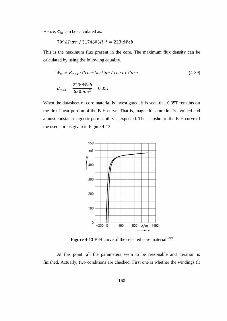
160
Hence, can be calculated as:
This is the maximum flux present in the core. The maximum flux density can be
calculated by using the following equality.
(4-39)
When the datasheet of core material is investigated, it is seen that 0.35T remains on
the first linear portion of the B-H curve. That is, magnetic saturation is avoided and
almost constant magnetic permeability is expected. The snapshot of the B-H curve of
the used core is given in Figure 4-13.
Figure 4-13 B-H curve of the selected core material [30]
At this point, all the parameters seem to be reasonable and iteration is
finished. Actually, two conditions are checked. First one is whether the windings fit
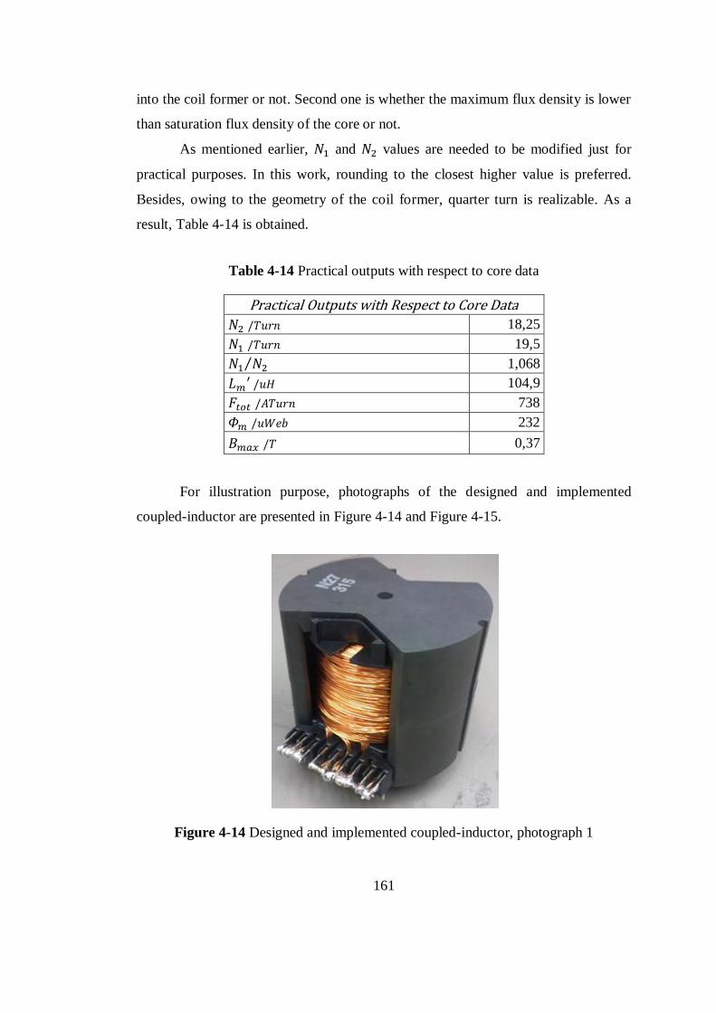
161
into the coil former or not. Second one is whether the maximum flux density is lower
than saturation flux density of the core or not.
As mentioned earlier, and values are needed to be modified just for
practical purposes. In this work, rounding to the closest higher value is preferred.
Besides, owing to the geometry of the coil former, quarter turn is realizable. As a
result, Table 4-14 is obtained.
Table 4-14 Practical outputs with respect to core data
Practical Outputs with Respect to Core Data
18,25
19,5
1,068
104,9
738
232
0,37
For illustration purpose, photographs of the designed and implemented
coupled-inductor are presented in Figure 4-14 and Figure 4-15.
Figure 4-14 Designed and implemented coupled-inductor, photograph 1
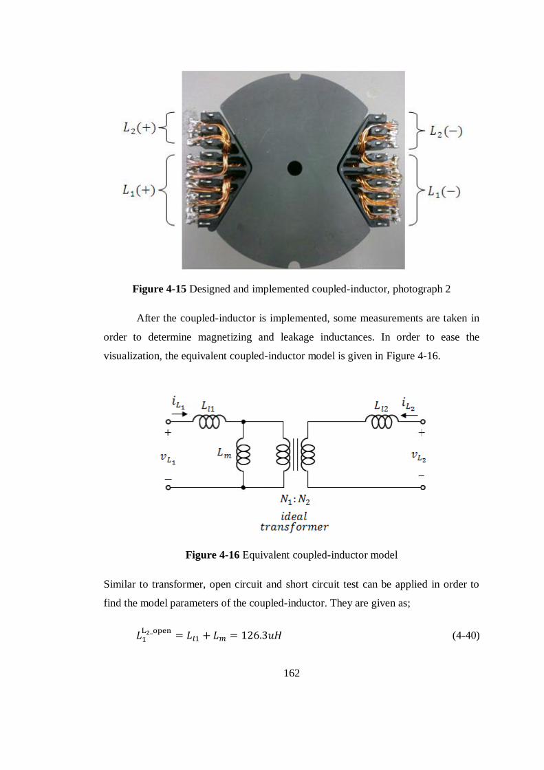
162
Figure 4-15 Designed and implemented coupled-inductor, photograph 2
After the coupled-inductor is implemented, some measurements are taken in
order to determine magnetizing and leakage inductances. In order to ease the
visualization, the equivalent coupled-inductor model is given in Figure 4-16.
Figure 4-16 Equivalent coupled-inductor model
Similar to transformer, open circuit and short circuit test can be applied in order to
find the model parameters of the coupled-inductor. They are given as;
(4-40)

163
(4-41)
(4-42)
(4-43)
(4-40)-(4-41) or (4-42)-(4-43) can used in order to determine the parameters:
, and . By the way, the following assumptions are utilized in order to find a
solution set.
and (4-44)
When the measurements belonging to the first winding side are used, the following
parameters are found.
As mentioned in CHAPTER 2, must be equal to in order to satisfy ripple-free
input current waveform condition.
From the calculations above, it is seen that there is a difference between and .
As mentioned at the beginning, this difference is expected. As a solution, an
„adjustment‟ inductor is used as an addition to the leakage inductance .
Adding a discrete inductor with the value of 6.2uH in series with positive terminal of
winding satisfies the condition, thereby providing ripple-free input current at all
operating points. As a consequence, the following model and parameters are valid
from now on.

164
Figure 4-17 Adjusted coupled-inductor model and its parameters
Whether the adjustment inductor approach is correct or not will be checked
by simulation. For this purpose , and values can be deduced in the
following manner.
As an addition to the above values, the following values are used in the simulation.
Simulation is performed with the ideal elements in order not to mix the reverse effect
of parasitic elements with the possible failure of the approach. It is performed at
, and full load. Validity of the approach can be verified by the
help of Figure 4-18 and Figure 4-19. As seen in Figure 4-18, the envelope of the
input current is very narrow. When a closer look is taken at the input current in
Figure 4-19, it is seen that the percent of the peak-to-peak current ripple is less than
0.2%. As a result, the approach is validated.
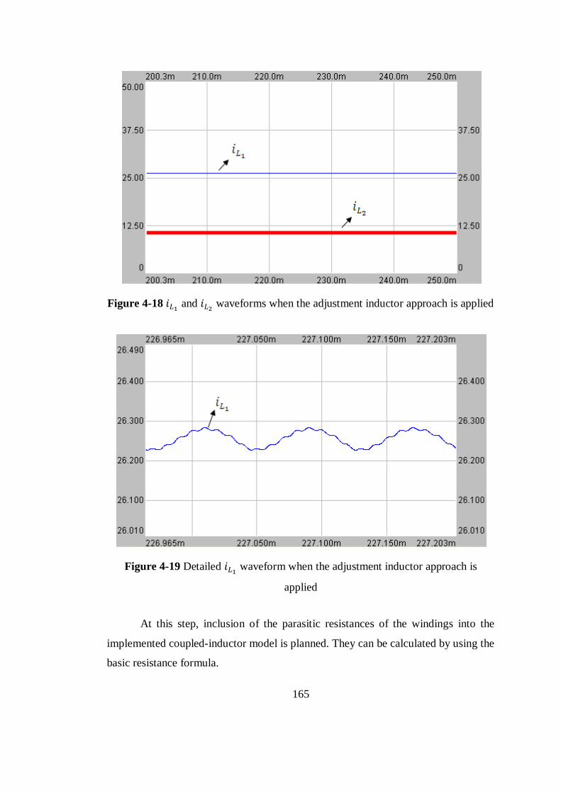
165
Figure 4-18 and
waveforms when the adjustment inductor approach is applied
Figure 4-19 Detailed waveform when the adjustment inductor approach is
applied
At this step, inclusion of the parasitic resistances of the windings into the
implemented coupled-inductor model is planned. They can be calculated by using the
basic resistance formula.

166
(4-45)
As used earlier, for copper. Cross section area of a single wire
was calculated as 0.24mm2 in the previous analyses. L is the mean length of a single
wire. Mean length path is shown in Figure 4-20. It is assumed that all the wires pass
through the mid-circle between the inner and output circles of the coil former.
Figure 4-20 Mean length path of the coil former [31]
Diameter and perimeter of the circle are calculated as:
Firstly, let‟s calculate the parasitic resistance of winding. Resistance of a single
wire is calculated easily.
As given in Table 4-11, there are 30 parallel wires.

167
Parasitic resistance of winding is calculated similarly.
As presented in Table 4-11, there exist 12 parallel wires in winding.
Parasitic resistance of the adjustment inductor should be considered as well.
As mentioned earlier, 6.2uH is required. In order to obtain this inductance value, 3 of
2uH inductor is decided to use. Note that rather than 6.2uH, 6uH will be used due to
the availability of the inductors. This much inconsistency may also stem from the
measurement error of the coupled-inductor parameters or the parasitic elements
easily. Therefore, trying to find exactly 6.2uH is regarded as a useless effort.
Necessary data of the selected adjustment inductor is given as;
Company: Coilcraft Part Number: SER2010-202MLB
Core Type: Ferrite
Since 3 of it will be used in series, total resistance is 3mΩ.
As a result, equivalent coupled-inductor model with parasitic resistances can be
formed. It is seen in Figure 4-21.
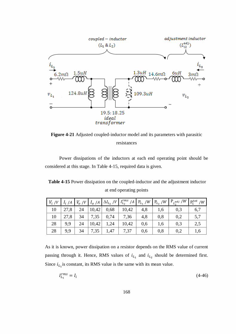
168
Figure 4-21 Adjusted coupled-inductor model and its parameters with parasitic
resistances
Power dissipations of the inductors at each end operating point should be
considered at this stage. In Table 4-15, required data is given.
Table 4-15 Power dissipation on the coupled-inductor and the adjustment inductor
at end operating points
10 27,8 24 10,42 0,68 10,42 4,8 1,6 0,3 6,7
10 27,8 34 7,35 0,74 7,36 4,8 0,8 0,2 5,7
28 9,9 24 10,42 1,24 10,42 0,6 1,6 0,3 2,5
28 9,9 34 7,35 1,47 7,37 0,6 0,8 0,2 1,6
As it is known, power dissipation on a resistor depends on the RMS value of current
passing through it. Hence, RMS values of and
should be determined first.
Since is constant, its RMS value is the same with its mean value.
(4-46)

169
As shown in Figure 4-8, has a dc level and ac triangular waveform superimposed
on dc level.
(4-47)
Its dc level is equal to . Peak-to-peak magnitude of is labeled as
. ac
triangular waveform is not necessarily equal i.e. duty-factor is generally different
than 0.5. By using the RMS value definition in (4-3),
can be found in the
following manner. Since its ripple percent is very low,
is expected to be very
close to its mean value. Still, the analysis seems to be necessary as a check.
(4-48)
(4-49)
Note that the integral of is zero.
(4-50)
By using (4-29), the following data can be inferred.
(4-51)
As a consequence,
can be expressed in the simplest form as;
(4-52)
As seen in Table 4-15,
turns out to be closer to as expected.
Once the RMS values of currents are obtained, power dissipations on the
inductors can be calculated. As observed in Table 4-15, most of the power is
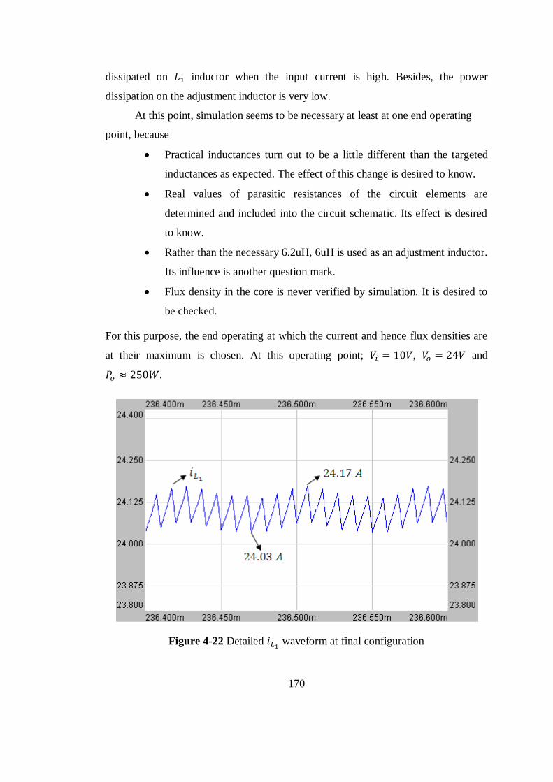
170
dissipated on inductor when the input current is high. Besides, the power
dissipation on the adjustment inductor is very low.
At this point, simulation seems to be necessary at least at one end operating
point, because
Practical inductances turn out to be a little different than the targeted
inductances as expected. The effect of this change is desired to know.
Real values of parasitic resistances of the circuit elements are
determined and included into the circuit schematic. Its effect is desired
to know.
Rather than the necessary 6.2uH, 6uH is used as an adjustment inductor.
Its influence is another question mark.
Flux density in the core is never verified by simulation. It is desired to
be checked.
For this purpose, the end operating at which the current and hence flux densities are
at their maximum is chosen. At this operating point; , and
.
Figure 4-22 Detailed waveform at final configuration
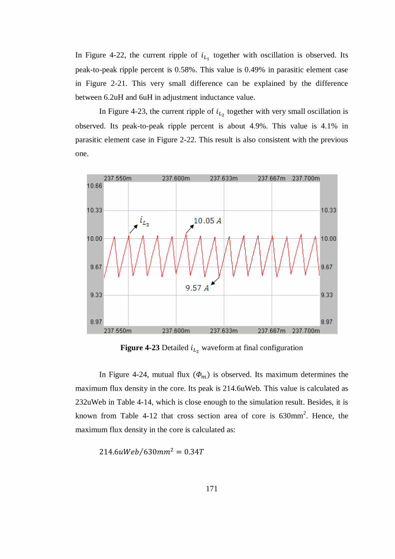
171
In Figure 4-22, the current ripple of together with oscillation is observed. Its
peak-to-peak ripple percent is 0.58%. This value is 0.49% in parasitic element case
in Figure 2-21. This very small difference can be explained by the difference
between 6.2uH and 6uH in adjustment inductance value.
In Figure 4-23, the current ripple of together with very small oscillation is
observed. Its peak-to-peak ripple percent is about 4.9%. This value is 4.1% in
parasitic element case in Figure 2-22. This result is also consistent with the previous
one.
Figure 4-23 Detailed waveform at final configuration
In Figure 4-24, mutual flux is observed. Its maximum determines the
maximum flux density in the core. Its peak is 214.6uWeb. This value is calculated as
232uWeb in Table 4-14, which is close enough to the simulation result. Besides, it is
known from Table 4-12 that cross section area of core is 630mm2. Hence, the
maximum flux density in the core is calculated as:
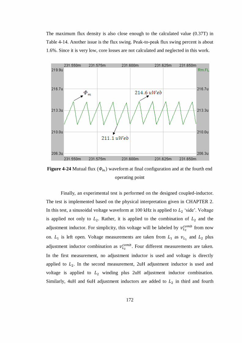
172
The maximum flux density is also close enough to the calculated value (0.37T) in
Table 4-14. Another issue is the flux swing. Peak-to-peak flux swing percent is about
1.6%. Since it is very low, core losses are not calculated and neglected in this work.
Figure 4-24 Mutual flux waveform at final configuration and at the fourth end
operating point
Finally, an experimental test is performed on the designed coupled-inductor.
The test is implemented based on the physical interpretation given in CHAPTER 2.
In this test, a sinusoidal voltage waveform at 100 kHz is applied to „side‟. Voltage
is applied not only to . Rather, it is applied to the combination of and the
adjustment inductor. For simplicity, this voltage will be labeled by
from now
on. is left open. Voltage measurements are taken from as and plus
adjustment inductor combination as
. Four different measurements are taken.
In the first measurement, no adjustment inductor is used and voltage is directly
applied to . In the second measurement, 2uH adjustment inductor is used and
voltage is applied to winding plus 2uH adjustment inductor combination.
Similarly, 4uH and 6uH adjustment inductors are added to in third and fourth
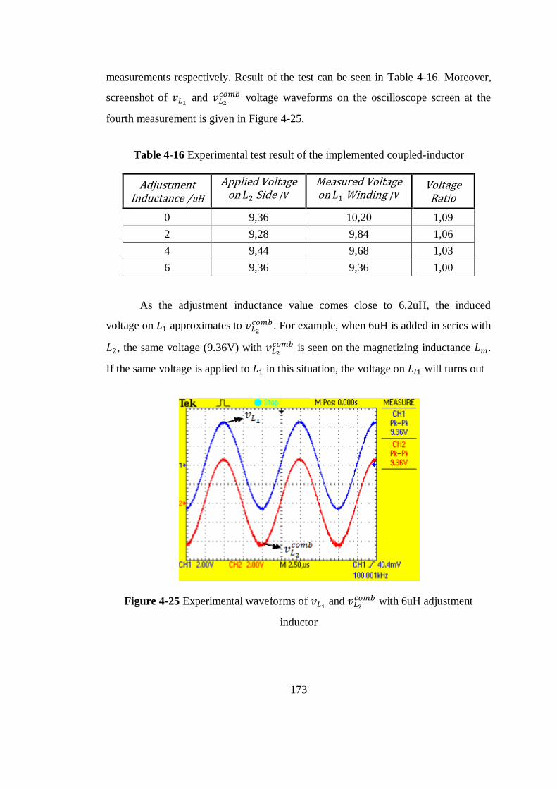
173
measurements respectively. Result of the test can be seen in Table 4-16. Moreover,
screenshot of and
voltage waveforms on the oscilloscope screen at the
fourth measurement is given in Figure 4-25.
Table 4-16 Experimental test result of the implemented coupled-inductor
Adjustment Inductance /uH
Applied Voltage on Side
Measured Voltage on Winding
Voltage Ratio
0 9,36 10,20 1,09
2 9,28 9,84 1,06
4 9,44 9,68 1,03
6 9,36 9,36 1,00
As the adjustment inductance value comes close to 6.2uH, the induced
voltage on approximates to
. For example, when 6uH is added in series with
, the same voltage (9.36V) with
is seen on the magnetizing inductance .
If the same voltage is applied to in this situation, the voltage on will turns out
Figure 4-25 Experimental waveforms of and
with 6uH adjustment
inductor

174
to be zero. It means that remains the same and ripple-free input current
requirement is satisfied.

175
CHAPTER 5
CONTROLLER DESIGN
5.1 INTRODUCTION
The design of the controller for the implemented circuit will be given in this
chapter. For this purpose, the transfer functions obtained in CHAPTER 3 using state-
space averaging method will be utilized.
There are no well-defined criteria set at the beginning for the controller. As
mentioned earlier, the converter will be used in parallel with li-ion battery pack,
which has a voltage changing between 24V-33.6V. There is also a switching voltage
regulator at the front end of the system, namely the military equipment. For this
reason, there is not any strict voltage regulation requirement. The input voltage range
of the system is 16V-55V. Probably, input current waveform requirement is more
restrictive. Circuit breaker or fuse at the cigarette lighter adapter of a vehicle should
not be activated, especially at the transient instants. Although the restrictions are
relatively looser and not well-defined, the controller performance is tried to keep as
high as possible.
At the very beginning, selection of the control technique in terms of analog or
digital is considered. Speed of analog control is compared with modifiability of
digital control. Element of analog control is the hardware composed of operational
amplifier, capacitors and resistor. Since what type of a controller would be used was
not known at the beginning, many analog controller hardware infrastructures would

176
be reserved on printed circuit board. However, digital controller element is just
software in a microcontroller, which is very easy to modify. In order to utilize this
advantage of digital control, it must be verified that the speed of digital control is
enough for this application. Then, the maximum speed of the microcontrollers in the
market has been searched. Microchip‟s digital signal controller family specialized for
switched-mode power supply applications is considered to be very reasonable for this
purpose. At first sight, it seemed to be possible to close the control loop at each
PWM cycle, 10 usec here. When the comparison of PWM carrier signal with the
duty-factor reference signal in analog control is considered, the control loop
frequency is equal to PWM frequency there. That is, the speed of a digital control
may reach that of analog control. Hence, the speed disadvantage of digital control is
considered to be overcome by using a Microchip‟s digital signal controller
specialized for SMPS applications. As a result, digital control has been preferred.
Among that controller family, dsPIC30F2020 was chosen because of its minimum
number of peripherals. Three analog input channels (analog-to-digital conversion of
output voltage, input current and input voltage), one PWM output and one general
purpose input channel (mode selection between constant input current mode -CICM-
and constant input power mode -CIPM-) is required in this application. Despite its
minimum number of peripherals in that family, dsPIC30F2020 highly covers the
need of this application.
Which control method, voltage mode control or current mode control, would
be used was also be evaluated. Since the input current is required to control in both
modes, namely CICM and CIPM, while limiting the output voltage to a set value of
34V, it is inevitable to use current mode control. In this method, input inductor
current, (or ) and output capacitor voltage,
(or ) are controlled in a
cascaded manner. Since the input current can change faster than the output voltage, it
is placed the inner loop. Output voltage loop is the outer control loop and gives a
reference value for the input current according to the output voltage. Although
current mode control is adopted in a reasonable manner, voltage mode control has
also been examined. Before a more complicated current mode control, simpler

177
voltage mode control has been desired to implement as an intermediate step. Voltage
mode control simulations performed in Simplorer with many different controller
parameters did not give a stable output voltage. There existed a small amplitude
oscillation around the reference value. Oscillation frequency was the same with the
frequency of the nearest pole of the duty-factor-to-output voltage transfer function,
to the origin in s-domain. Then, voltage mode control was applied on the
implemented circuit experimentally and the same oscillation was observed. In that
situation, a large oscillation in the input current was realized. With this high
amplitude oscillation in input current, output voltage oscillation seemed to be
inevitable. Since the ultimate aim is current mode control, further elaboration in
voltage mode control was not performed and directly jumped to current mode
control. Since current mode control has been performed easily and consistent with
the calculations, voltage mode control of this circuit has then been evaluated as not
easily applicable.
In the inner and outer control loops, PI controller is preferred. It is known that
integral term lets the steady-state error be zero, which is a desired goal. Besides, in
most of the industrial applications, PI controller is seen satisfactory. Therefore, PI
controller is implemented as a first choice and gives a satisfactory result. Hence,
other controller types are not tried.
Up to this point, the controller scheme is drawn roughly and it will be
detailed in the following sections. According to the control block diagram and the
related transfer functions found earlier, necessary controller functions will be
obtained in s-domain. Then, using a bilinear transformation, controller functions will
be converted into their z-domain correspondence. By inverse z-transformation,
controller functions in discrete time domain will be obtained. Then, those functions
will be embedded to dsPIC.
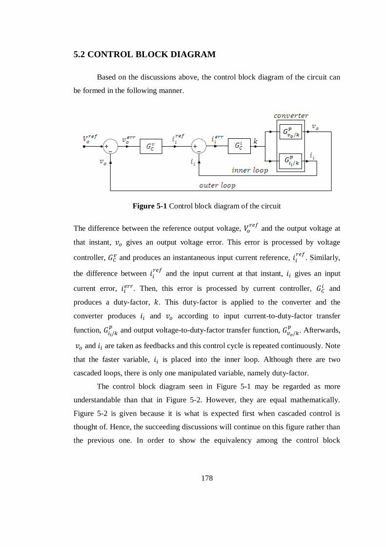
178
5.2 CONTROL BLOCK DIAGRAM
Based on the discussions above, the control block diagram of the circuit can
be formed in the following manner.
Figure 5-1 Control block diagram of the circuit
The difference between the reference output voltage,
and the output voltage at
that instant, gives an output voltage error. This error is processed by voltage
controller, and produces an instantaneous input current reference,
. Similarly,
the difference between
and the input current at that instant, gives an input
current error, . Then, this error is processed by current controller,
and
produces a duty-factor, . This duty-factor is applied to the converter and the
converter produces and according to input current-to-duty-factor transfer
function,
and output voltage-to-duty-factor transfer function,
. Afterwards,
and are taken as feedbacks and this control cycle is repeated continuously. Note
that the faster variable, is placed into the inner loop. Although there are two
cascaded loops, there is only one manipulated variable, namely duty-factor.
The control block diagram seen in Figure 5-1 may be regarded as more
understandable than that in Figure 5-2. However, they are equal mathematically.
Figure 5-2 is given because it is what is expected first when cascaded control is
thought of. Hence, the succeeding discussions will continue on this figure rather than
the previous one. In order to show the equivalency among the control block
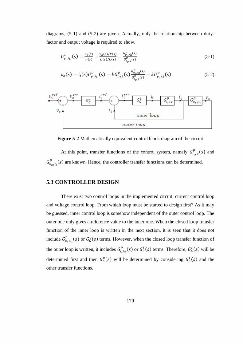
179
diagrams, (5-1) and (5-2) are given. Actually, only the relationship between duty-
factor and output voltage is required to show.
(5-1)
(5-2)
Figure 5-2 Mathematically equivalent control block diagram of the circuit
At this point, transfer functions of the control system, namely and
are known. Hence, the controller transfer functions can be determined.
5.3 CONTROLLER DESIGN
There exist two control loops in the implemented circuit: current control loop
and voltage control loop. From which loop must be started to design first? As it may
be guessed, inner control loop is somehow independent of the outer control loop. The
outer one only gives a reference value to the inner one. When the closed loop transfer
function of the inner loop is written in the next section, it is seen that it does not
include
or terms. However, when the closed loop transfer function of
the outer loop is written, it includes or
terms. Therefore, will be
determined first and then will be determined by considering
and the
other transfer functions.
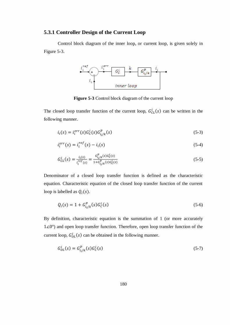
180
5.3.1 Controller Design of the Current Loop
Control block diagram of the inner loop, or current loop, is given solely in
Figure 5-3.
Figure 5-3 Control block diagram of the current loop
The closed loop transfer function of the current loop, can be written in the
following manner.
(5-3)
(5-4)
(5-5)
Denominator of a closed loop transfer function is defined as the characteristic
equation. Characteristic equation of the closed loop transfer function of the current
loop is labelled as .
(5-6)
By definition, characteristic equation is the summation of 1 (or more accurately
) and open loop transfer function. Therefore, open loop transfer function of the
current loop, can be obtained in the following manner.
(5-7)

181
At this point, must be known in order design a current compensator,
.
, or the other transfer functions derived before, has the following terms
parametrically:
and . Note that other than the circuit parameters, also operating point parameters
take place in the transfer functions. In other words, the converter‟s transfer function
changes as the operating point changes. As expected, transfer functions at different
operating points are calculated and it is seen that there are only minor differences
between the pole and zero locations of the transfer functions. Therefore, an operating
point can be chosen and the transfer functions can be calculated at that point. Here,
the first end operating point ( and at full load) is chosen
randomly. As a result; is calculated in Matlab using the derived parametric
transfer function in CHAPTER 3, the implemented circuit parameters and the
numerical values of the operating point parameters.
(5-8)
In order to get acquainted with , its pole-zero map in s-domain is given in
Figure 5-4. Blue circles represent zeros and blue x‟s are used for poles. At the left
figure, all poles and zeros of the related transfer function is shown but not seen
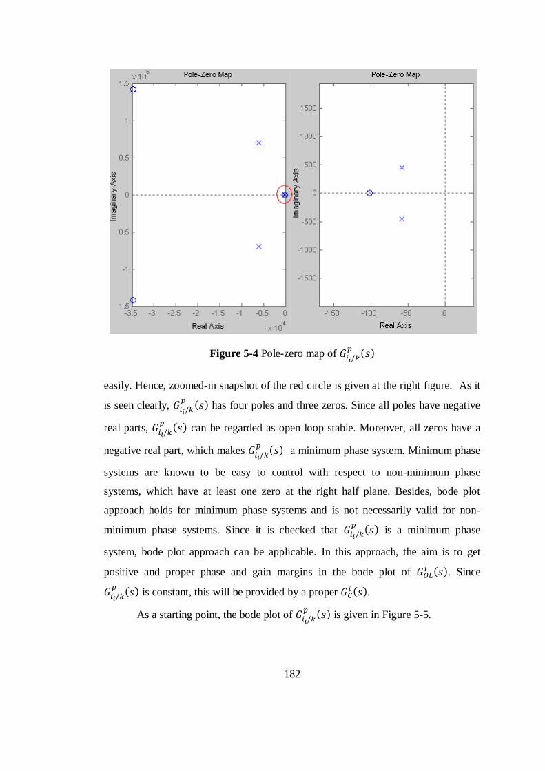
182
Figure 5-4 Pole-zero map of
easily. Hence, zoomed-in snapshot of the red circle is given at the right figure. As it
is seen clearly, has four poles and three zeros. Since all poles have negative
real parts, can be regarded as open loop stable. Moreover, all zeros have a
negative real part, which makes a minimum phase system. Minimum phase
systems are known to be easy to control with respect to non-minimum phase
systems, which have at least one zero at the right half plane. Besides, bode plot
approach holds for minimum phase systems and is not necessarily valid for non-
minimum phase systems. Since it is checked that is a minimum phase
system, bode plot approach can be applicable. In this approach, the aim is to get
positive and proper phase and gain margins in the bode plot of . Since
is constant, this will be provided by a proper
.
As a starting point, the bode plot of is given in Figure 5-5.
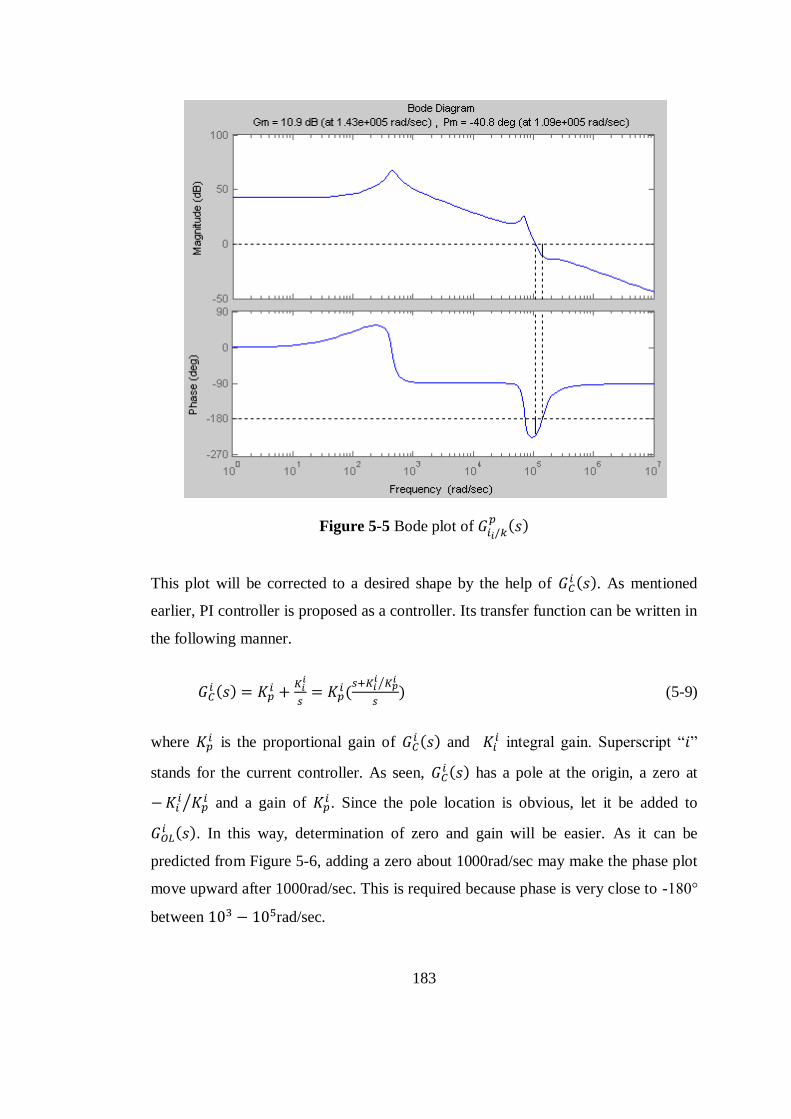
183
Figure 5-5 Bode plot of
This plot will be corrected to a desired shape by the help of . As mentioned
earlier, PI controller is proposed as a controller. Its transfer function can be written in
the following manner.
(5-9)
where is the proportional gain of
and integral gain. Superscript “ ”
stands for the current controller. As seen, has a pole at the origin, a zero at
and a gain of . Since the pole location is obvious, let it be added to
. In this way, determination of zero and gain will be easier. As it can be
predicted from Figure 5-6, adding a zero about 1000rad/sec may make the phase plot
move upward after 1000rad/sec. This is required because phase is very close to -180°
between rad/sec.
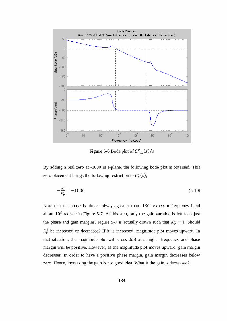
184
Figure 5-6 Bode plot of
By adding a real zero at -1000 in s-plane, the following bode plot is obtained. This
zero placement brings the following restriction to ;
(5-10)
Note that the phase is almost always greater than -180° expect a frequency band
about rad/sec in Figure 5-7. At this step, only the gain variable is left to adjust
the phase and gain margins. Figure 5-7 is actually drawn such that . Should
be increased or decreased? If it is increased, magnitude plot moves upward. In
that situation, the magnitude plot will cross 0dB at a higher frequency and phase
margin will be positive. However, as the magnitude plot moves upward, gain margin
decreases. In order to have a positive phase margin, gain margin decreases below
zero. Hence, increasing the gain is not good idea. What if the gain is decreased?
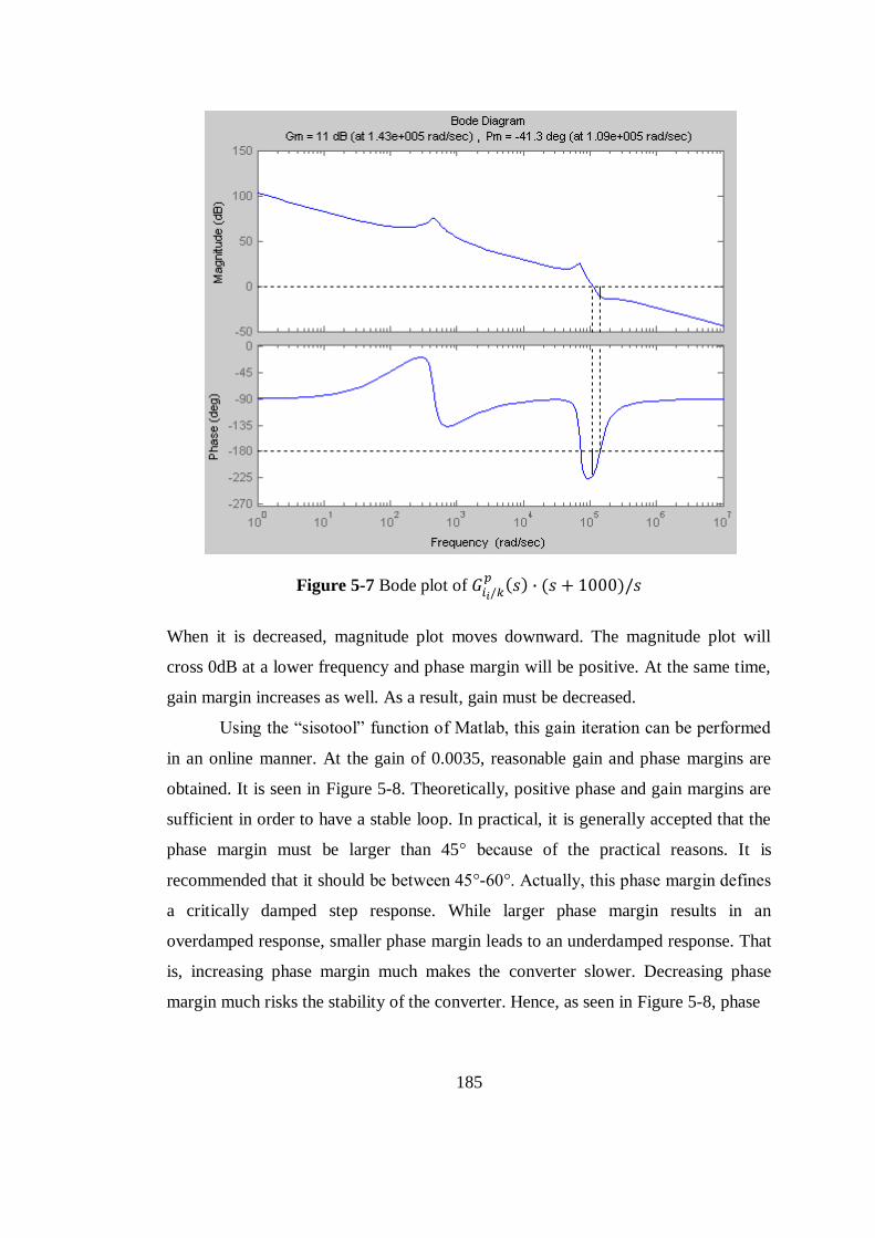
185
Figure 5-7 Bode plot of
When it is decreased, magnitude plot moves downward. The magnitude plot will
cross 0dB at a lower frequency and phase margin will be positive. At the same time,
gain margin increases as well. As a result, gain must be decreased.
Using the “sisotool” function of Matlab, this gain iteration can be performed
in an online manner. At the gain of 0.0035, reasonable gain and phase margins are
obtained. It is seen in Figure 5-8. Theoretically, positive phase and gain margins are
sufficient in order to have a stable loop. In practical, it is generally accepted that the
phase margin must be larger than 45° because of the practical reasons. It is
recommended that it should be between 45°-60°. Actually, this phase margin defines
a critically damped step response. While larger phase margin results in an
overdamped response, smaller phase margin leads to an underdamped response. That
is, increasing phase margin much makes the converter slower. Decreasing phase
margin much risks the stability of the converter. Hence, as seen in Figure 5-8, phase
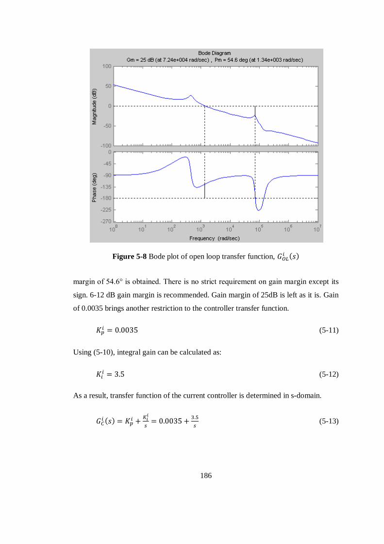
186
Figure 5-8 Bode plot of open loop transfer function,
margin of 54.6° is obtained. There is no strict requirement on gain margin except its
sign. 6-12 dB gain margin is recommended. Gain margin of 25dB is left as it is. Gain
of 0.0035 brings another restriction to the controller transfer function.
(5-11)
Using (5-10), integral gain can be calculated as:
(5-12)
As a result, transfer function of the current controller is determined in s-domain.
(5-13)
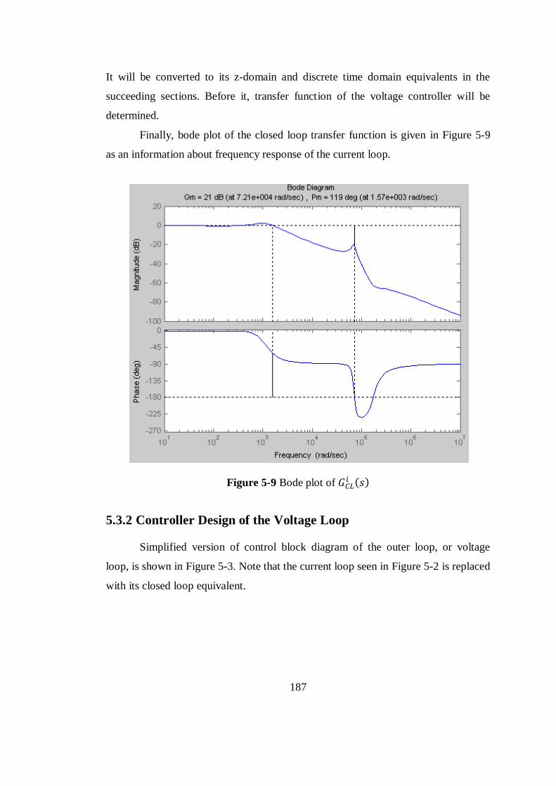
187
It will be converted to its z-domain and discrete time domain equivalents in the
succeeding sections. Before it, transfer function of the voltage controller will be
determined.
Finally, bode plot of the closed loop transfer function is given in Figure 5-9
as an information about frequency response of the current loop.
Figure 5-9 Bode plot of
5.3.2 Controller Design of the Voltage Loop
Simplified version of control block diagram of the outer loop, or voltage
loop, is shown in Figure 5-3. Note that the current loop seen in Figure 5-2 is replaced
with its closed loop equivalent.

188
Figure 5-10 Control block diagram of the voltage loop
The closed loop transfer function of the voltage loop, can be written in the
following manner.
(5-14)
(5-15)
(5-16)
By using definition in (5-5) and
definition in (5-1), more simplified
version of can be obtained. It can be observed in (5-17). Note that
includes all the transfer functions that exist in the cascaded loop.
(5-17)
As performed in the current loop, characteristic equation of the closed loop transfer
function of the voltage loop, can be written similarly.
(5-18)
Then, open loop transfer function of the voltage loop, can be obtained in the
following manner.
(5-19)
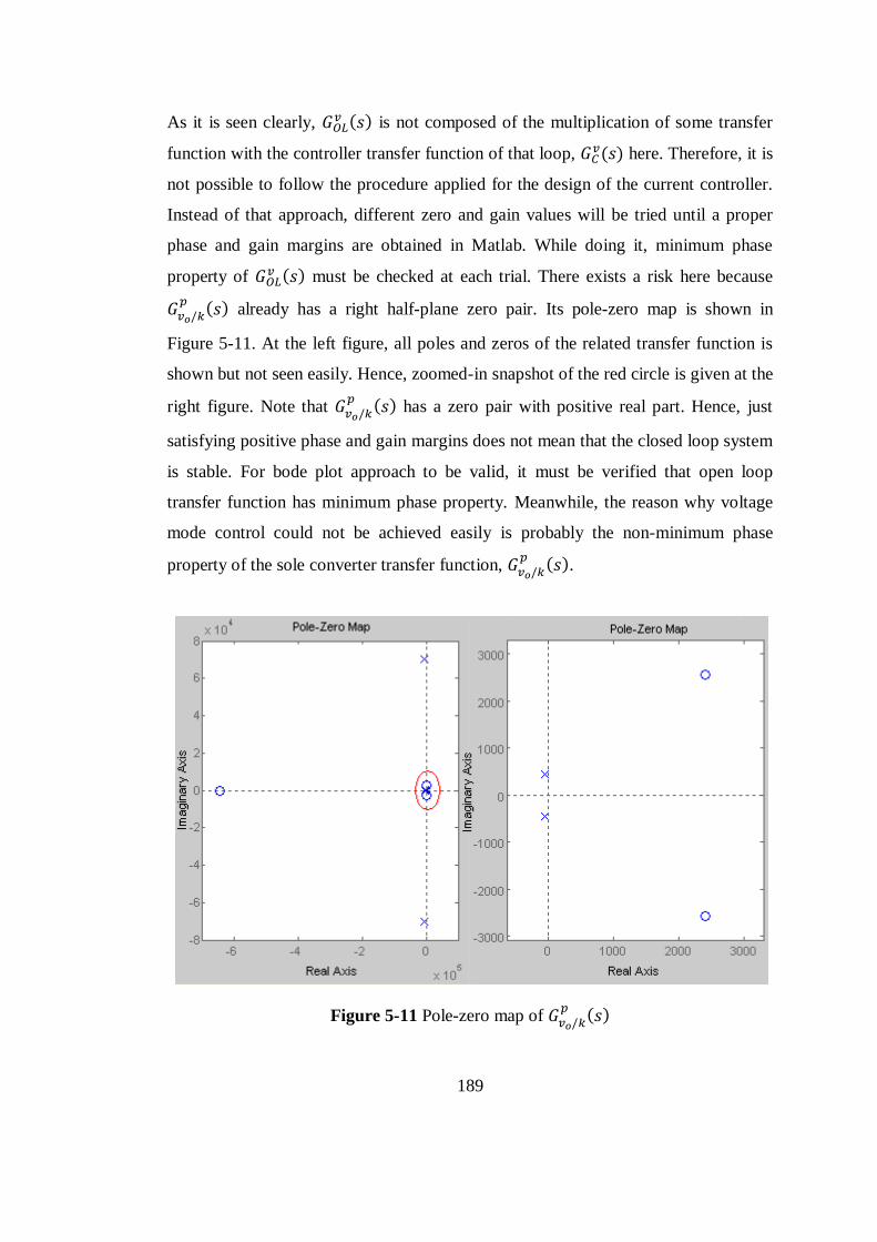
189
As it is seen clearly, is not composed of the multiplication of some transfer
function with the controller transfer function of that loop, here. Therefore, it is
not possible to follow the procedure applied for the design of the current controller.
Instead of that approach, different zero and gain values will be tried until a proper
phase and gain margins are obtained in Matlab. While doing it, minimum phase
property of must be checked at each trial. There exists a risk here because
already has a right half-plane zero pair. Its pole-zero map is shown in
Figure 5-11. At the left figure, all poles and zeros of the related transfer function is
shown but not seen easily. Hence, zoomed-in snapshot of the red circle is given at the
right figure. Note that has a zero pair with positive real part. Hence, just
satisfying positive phase and gain margins does not mean that the closed loop system
is stable. For bode plot approach to be valid, it must be verified that open loop
transfer function has minimum phase property. Meanwhile, the reason why voltage
mode control could not be achieved easily is probably the non-minimum phase
property of the sole converter transfer function, .
Figure 5-11 Pole-zero map of

190
As mentioned earlier, again PI controller is proposed as a controller. Its
transfer function can be written in the following manner.
(5-20)
where is the proportional gain of
and integral gain. Superscript “ ”
stands for the voltage controller. Now, the aim is to find a voltage controller transfer
function that gives proper phase and gain margins. After several zero and gain trial in
Matlab, the following values is determined.
(5-21)
(5-22)
Therefore, is calculated as:
(5-23)
As a result, transfer function of the voltage controller turn out to be:
(5-24)
Now, minimum phase property must be checked in order to rely on bode plot.
Pole-zero map of is given in Figure 5-12. The same arguments about reading
the pole-zero maps also hold here. Besides, as it can be guessed, some poles and
zeros coincide. This is because of the fact that Matlab does not perform pole-zero
cancellation. It is seen that all poles and zeros have negative real parts. In other
words, it is a minimum phase system.
Bode plot of is shown in Figure 5-13. As it is seen, phase margin is
56° and gain margin is 26.9 dB, which are reasonable values as mentioned earlier.
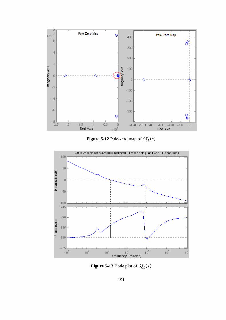
191
Figure 5-12 Pole-zero map of
Figure 5-13 Bode plot of
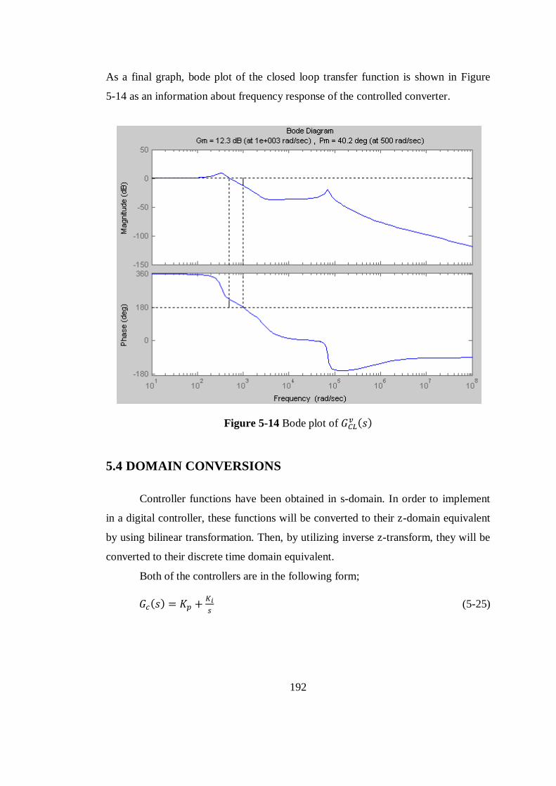
192
As a final graph, bode plot of the closed loop transfer function is shown in Figure
5-14 as an information about frequency response of the controlled converter.
Figure 5-14 Bode plot of
5.4 DOMAIN CONVERSIONS
Controller functions have been obtained in s-domain. In order to implement
in a digital controller, these functions will be converted to their z-domain equivalent
by using bilinear transformation. Then, by utilizing inverse z-transform, they will be
converted to their discrete time domain equivalent.
Both of the controllers are in the following form;
(5-25)

193
There are few s-domain to z-domain transformation types. Bilinear transformation
has been applied and given a satisfactory result. Hence, it will be given in this
section. According to bilinear transformation, the following conversion is performed:
(5-26)
where is the sampling frequency. Therefore, controller transfer function in z-
domain, can be obtained in the following manner.
(5-27)
(5-28)
At this stage, input-output relationship of the controller can be formed. Let the
controller input be and output be . While they will be named as and
in z-domain, they are called and in discrete time domain. Hence, the
following relationship exists.
(5-29)
(5-30)
(5-31)
By using inverse z-transform, (5-31) is converted to its discrete time equivalent.
(5-32)
What does (5-32) mean? is the current output of the controller and is
the previous output. is the input to the controller at that sampling instant and

194
is the previous sampled input. That is, the current output of the PI-
controller is determined based on the previous output, the input at that sampling
instant and the previous input. As a consequence, (5-32) is ready to implement in a
digital signal controller.
5.5 APPLICATION SPECIFIC POINTS
Main ideas about controller design are given so far. This section includes
some practical, complementary or application specific points, which are important as
well.
As mentioned in the design chapter, the implemented circuit has two
selectable modes: constant input current mode (CICM) and constant input power
mode (CIPM). These modes have only one difference in terms control. When Figure
5-15 is investigated, it is seen that the controller outputs are limited. Limiter at the
output of is required in order to limit duty-factor. Otherwise it could result in
shorting the switch for a relatively long time. This limit is chosen as 0.9 in this
application. This part is the same for both CICM and CIPM. However, the limiter at
the output of is different. It will limit the input current reference to 10A in
CICM and in CIPM. Input voltage will be sampled as an addition to
output voltage and input current at each sampling instant in CIPM. In this way, the
input current limit, which is the limit of
, is determined in order to draw at most
280W from the input.
Figure 5-15 Control block diagram with the limiters

195
When a limit is applied at the output of the controller, a precaution must be
taken. As long as the output of the controller is limited, its integral gain must be held
at zero. Otherwise, a wrong interpretation is made by controller, which is observed in
closed-loop simulations. As a result, the following “if statement” has been applied
and therefore the last term (the integral term) of the equation is dropped so that;
Generally, it is not possible to use the transfer functions directly. Because of
the voltage divisions in feedback paths, output range of the current sensors, analog-
to-digital conversion output range and PWM value range; transfer function is
normalized by a meaningful coefficients. For example, while duty-factor changes
between 0-0.9 in s-domain, it corresponds to 7-9240 bit value in the used digital
signal controller. Owing to these kinds of normalizations, coefficients are
multiplied by 613 in this application.
As it will be given in details, is determined as 1 switching period
( ) in CICM and 3 switching period in CIPM. When these values
considered, the revised transfer functions are obtained. Transfer functions are now
ready to use in digital signal controller.
In CICM:
Current Controller
(5-33)
Voltage Controller
(5-34)

196
In CIPM:
Current Controller
(5-35)
Voltage Controller
(5-36)

197
CHAPTER 6
EXPERIMENTAL RESULTS
6.1 INTRODUCTION
This chapter presents the experimental results of the designed and
implemented circuit running in open-loop and closed-loop modes. For illustration
purposes, its photographs are presented in Figure 6-1 and Figure 6-2, for a better
understanding of which one may refer to Figure 3-16 for the circuit diagram and
Figure 4-21 for the adjusted coupled-inductor model. At first, voltage and current
waveforms of the circuit elements are given and compared with the theoretical
analyses and the simulation results. Especially, the operation with the coupled-
inductor providing ripple-free input current is investigated. Efficiency measurements
at different operating points are also given. Secondly, closed-loop implementation
will be handled. Starting with the transfer functions obtained in CHAPTER 3,
necessary controller functions are determined and implemented via a
microcontroller, or more accurately digital signal controller. Then, the possible
dynamic responses of the circuit are given in order or evaluate the performance of
the controller implementation.
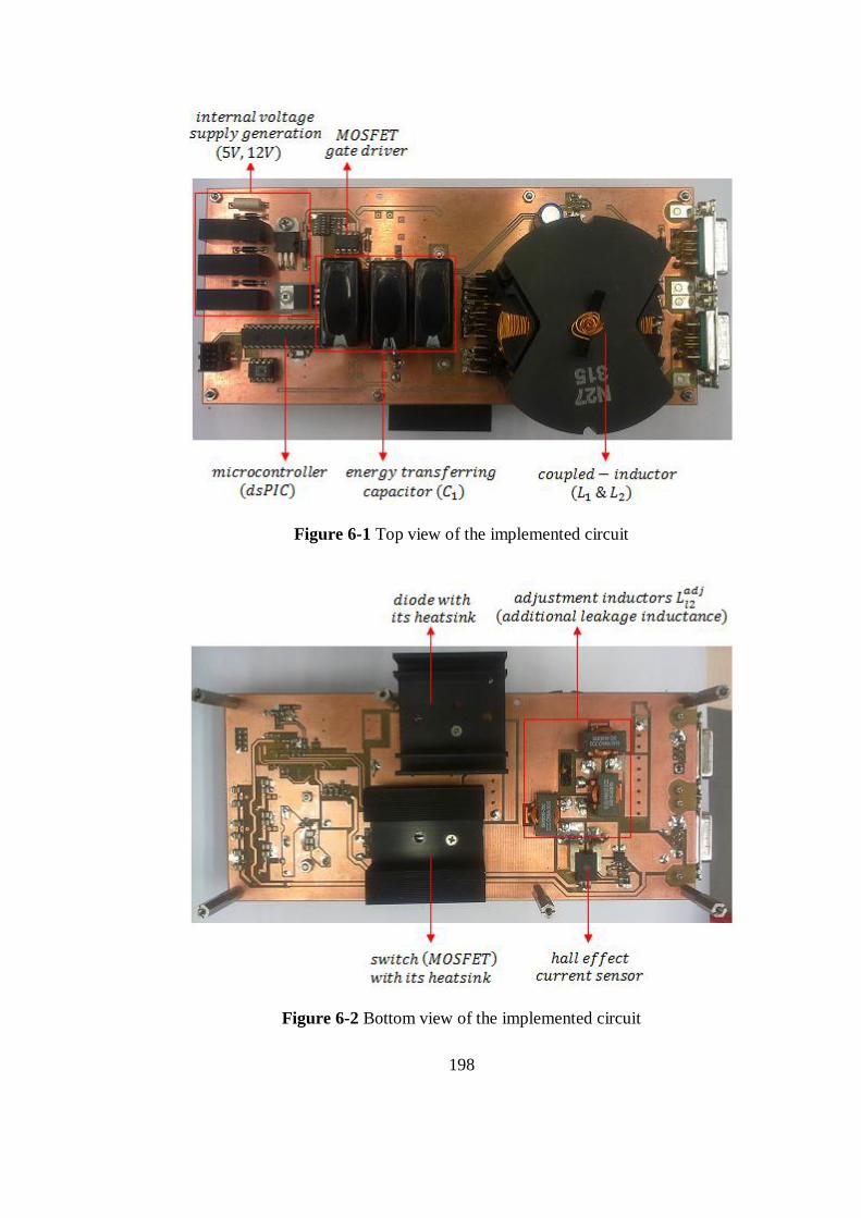
198
Figure 6-1 Top view of the implemented circuit
Figure 6-2 Bottom view of the implemented circuit

199
6.2 OPEN-LOOP RESULTS
In this section, important voltage and current waveforms of the implemented
circuit running in open-loop mode are presented as verifications. Moreover, the
efficiency of the converter in many operating points is given.
6.2.1 Voltage Waveforms
Important voltage waveforms of the switch, diode, output capacitor, input
inductor and output inductor are presented in order to verify the design and
implementation of the circuit.
6.2.1.1 Voltage Waveforms of the Switch and the Diode
Snapshots of the voltage waveforms are taken at two different operating
points. One of them is the first end operating point, at which the current stress is at its
maximum. Voltage overshoots due to the parasitic inductances of the paths carrying
pulsating currents are planned to observe at this point. Voltage overshoots may lead
to exceeding of the voltage ratings of the switch and diode. Another point is the
fourth end operating point, where voltage stress is at its maximum. This point is
regarded as another important operating point to investigate. All other operating
points are considered to be between these two end operating points in terms of
voltage stresses.
Voltage waveform of the switch at the first end operating point is seen in
Figure 6-3. As expected, the switch blocks ( 34V), which is represented by
„Cursor 2‟ in the figure. Note that the zero voltage level is represented by „1‟ at the
left of the figure. The peak value of is 62.4V, which is represented by „Cursor 1‟.
Voltage rating of the MOSFET is 100V. That is, it is high enough for safe operation.
There exists voltage overshoot of 28.8V, which is represented by „Delta‟. It is
considered as normal because almost 40A is switched in this situation. High
may easily result in that much voltage overshoots.

200
Figure 6-3 waveform at , and full load
Anode-to-cathode voltage of the diode, is presented in Figure 6-4 at the same
operating point. It blocks about similar to the switch. Its peak value is 53.6V.
Voltage rating of the diode is 170V, which can be considered as over safe. Moreover,
voltage overshoot on the diode is 21.6V.
Figure 6-4 waveform at , and full load
Voltage waveform of the switch at the fourth end operating point is seen in
Figure 6-5. The switch blocks 59.2V, which is close to its expected value of 62V in
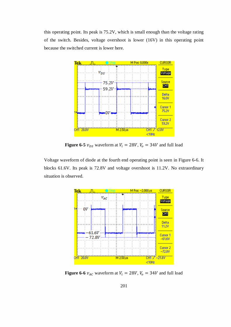
201
this operating point. Its peak is 75.2V, which is small enough than the voltage rating
of the switch. Besides, voltage overshoot is lower (16V) in this operating point
because the switched current is lower here.
Figure 6-5 waveform at , and full load
Voltage waveform of diode at the fourth end operating point is seen in Figure 6-6. It
blocks 61.6V. Its peak is 72.8V and voltage overshoot is 11.2V. No extraordinary
situation is observed.
Figure 6-6 waveform at , and full load

202
6.2.1.2 Voltage Waveforms of the Input and Output Inductors
Voltage waveforms of input and output inductors at the first and fourth
operating points are given as verification. As it is seen in Figure 6-7, is exposed to
the input voltage in Mode 1 and the inverse of the output voltage in Mode 2. This is
an expected waveform. Also, the same waveform is observed on the combination of
plus adjustment inductor,
. Since it is same as ,
is not given
intentionally. Instead, (i.e. without the adjustment inductor) is presented in
Figure 6-8. As it is aimed in the design process, high and low levels of are a little
bit lower than the cursors set at measurement. Another point must be highlighted:
Very high voltage overshoots are observed in the inductors. They stem from
measurement errors. When the terminals of the oscilloscope probe are long and form
a part of a sensitive loop, voltage spikes are observed at the switching instants. In this
measurement, minimizing this loop could not been performed. Hence, the waveforms
with voltage spikes have been presented obligatorily. Also, waveform has not
been given because of this reason. However, in measuring the voltage waveforms of
the other circuit elements, the positive effect of minimizing the loop of the probe has
been observed seriously. This problem and its solution are explained in Section 6.3.
Figure 6-7 waveform at , and full load

203
Figure 6-8 waveform at , and full load
The same arguments can also be applied in the fourth end operating point. As it is
understood from Figure 6-9 and Figure 6-10, inductor windings see 28V in Mode 1
and -34V in Mode 2. Again, is a little bit smaller than
in magnitude.
Figure 6-9 waveform at , and full load

204
Figure 6-10 waveform at , and full load
6.2.1.3 Voltage Waveforms of the Output Capacitor
Voltage waveforms of the output capacitor at the first and fourth operating
points are given as verification. In Figure 6-11, output voltage in the first operating
point is given. When the theoretical value of the duty-factor in this operating point is
calculated, it is found as 0.706. This figure is obtained at the duty-factor of 0.719,
Figure 6-11 waveform at , and full load
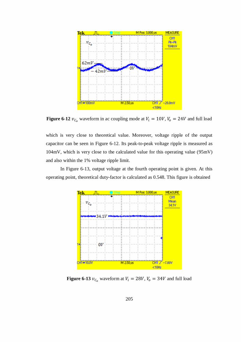
205
Figure 6-12 waveform in ac coupling mode at , and full load
which is very close to theoretical value. Moreover, voltage ripple of the output
capacitor can be seen in Figure 6-12. Its peak-to-peak voltage ripple is measured as
104mV, which is very close to the calculated value for this operating value (95mV)
and also within the 1% voltage ripple limit.
In Figure 6-13, output voltage at the fourth operating point is given. At this
operating point, theoretical duty-factor is calculated as 0.548. This figure is obtained
Figure 6-13 waveform at , and full load

206
Figure 6-14 waveform in ac coupling mode at , and full load
at the duty-factor of 0.550, which is very close to theoretical value. Also, voltage
ripple of the output capacitor can be seen in Figure 6-14. Its peak-to-peak voltage
ripple is measured as 280mV, which is very close to the calculated value for this
operating point, 207mV. By this way, the maximum of 1% voltage ripple condition
is satisfied in this operating point, which is the worst case.
6.2.2 Current Waveforms
In this section, current waveforms of the input and output inductors will be
given at two end operating points and three load levels. Two operating points are the
first and the fourth operating points. Three load levels are full load, 50% load and
10% load. As it is known, input inductor current is the input current itself. However,
output inductor current is not the output current exactly. It is flattened less or more
by the output capacitor. Hence, output capacitor is extracted from the circuit while
these current waveforms are being recorded in order to see the output inductor
current only.

207
6.2.2.1 and
Waveforms at the First End Operating Point
At this end operating point, the voltage levels are at their minimum and the
current levels are at their maximum. and
waveforms are observed while the
output power is about 250W, 125W and 25W.
6.2.2.1.1 and
Waveforms at Full Load for the First End
Operating Point
Input current waveform at the first end operating point and full load is
presented in Figure 6-15 and Figure 6-16. Note that the zero level is pointed as „4‟ at
the left of the figure. Current waveforms have been measured by a current probe.
While this measurement is taken, the scale of the current probe is at 50A/V. Hence,
mean value of the input current is calculated as:
Its peak-to-peak ripple current is also desired to show in Figure 6-15. However, since
the scale is high in this snapshot (100mV/div or 5A/div), it gives an incorrect value.
Hence, all ripple currents must be investigated in ac coupling mode and at low scale
in order to get more accurate results. As a result, the ripple current on the input
current in this operating condition is given in Figure 6-16. Its magnitude is very low
such that it cannot even show a repetitive waveform. Probably, the ripple current
magnitude is under the sensitivity of the measuring equipment. By accepting that the
measurement is valid, its magnitude is calculated as:
Therefore, peak-to-peak ripple percent of the input current is calculated as:
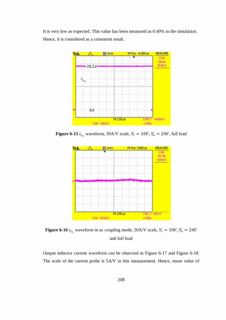
208
It is very low as expected. This value has been measured as 0.49% in the simulation.
Hence, it is considered as a consistent result.
Figure 6-15 waveform, 50A/V scale, , , full load
Figure 6-16 waveform in ac coupling mode, 50A/V scale, ,
and full load
Output inductor current waveform can be observed in Figure 6-17 and Figure 6-18.
The scale of the current probe is 5A/V in this measurement. Hence, mean value of
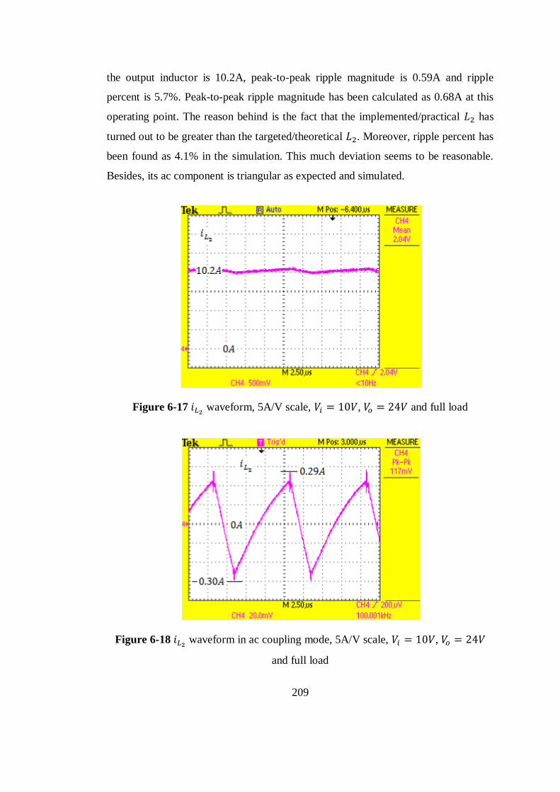
209
the output inductor is 10.2A, peak-to-peak ripple magnitude is 0.59A and ripple
percent is 5.7%. Peak-to-peak ripple magnitude has been calculated as 0.68A at this
operating point. The reason behind is the fact that the implemented/practical has
turned out to be greater than the targeted/theoretical . Moreover, ripple percent has
been found as 4.1% in the simulation. This much deviation seems to be reasonable.
Besides, its ac component is triangular as expected and simulated.
Figure 6-17 waveform, 5A/V scale, , and full load
Figure 6-18 waveform in ac coupling mode, 5A/V scale, ,
and full load

210
6.2.2.1.2 and
Waveforms at Half Load for the First End
Operating Point
Input current waveform at the first end operating point and 50% load is
presented in Figure 6-19 and Figure 6-20. As it can be calculated easily, mean value
of the input inductor current is 13.3A, peak-to-peak ripple magnitude is 0.042A and
ripple percent is 0.32%, which is very low as expected. Since the scale of the current
probe is 5A/V rather than 50A/V, it gives more accurate result at low current level.
This is probably why ripple current percent at 50% load turns out to be lower than
that at full load. Besides, ac component of the current resembles to a sinusoidal as
expected and simulated.
Figure 6-19 waveform, 5A/V scale, , and 50% load
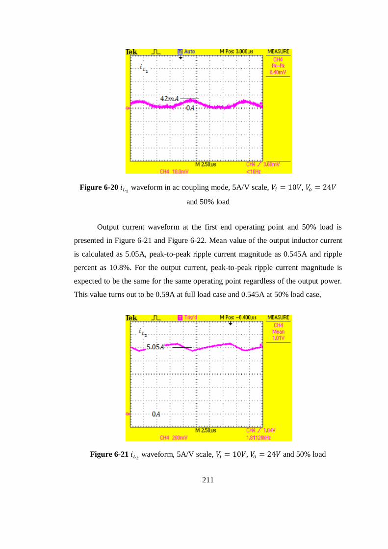
211
Figure 6-20 waveform in ac coupling mode, 5A/V scale, ,
and 50% load
Output current waveform at the first end operating point and 50% load is
presented in Figure 6-21 and Figure 6-22. Mean value of the output inductor current
is calculated as 5.05A, peak-to-peak ripple current magnitude as 0.545A and ripple
percent as 10.8%. For the output current, peak-to-peak ripple current magnitude is
expected to be the same for the same operating point regardless of the output power.
This value turns out to be 0.59A at full load case and 0.545A at 50% load case,
Figure 6-21 waveform, 5A/V scale, , and 50% load

212
Figure 6-22 waveform in ac coupling mode, 5A/V scale, ,
and 50% load
which are very close. Besides, since the mean value decreases while the ripple
magnitude remains the same, ripple current percent increases naturally. These results
are also regarded as consistent.
6.2.2.1.3 and
Waveforms at 10% Load for the First End
Operating Point
Input current waveform at the first end operating point and 10% load is
presented in Figure 6-23 and Figure 6-24. Mean value of the input inductor current is
calculated as 2.59A, peak-to-peak ripple magnitude is 0.044A and ripple percent is
1.7%. Ripple current magnitude is still very low but the mean value is lower at this
load level. Since the ripple current magnitude is not zero but very close to it due to
the practical issues, increase in ripple percent with decreasing load is inevitable. This
is also an expected result.
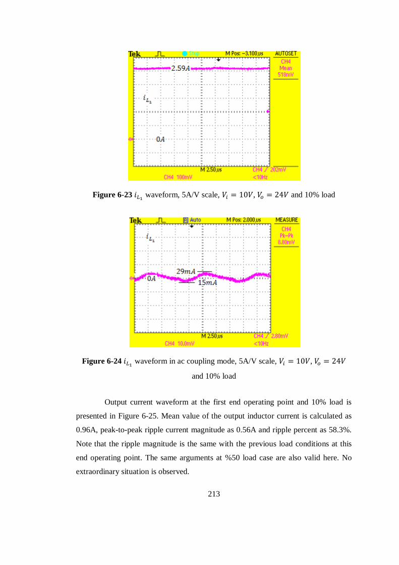
213
Figure 6-23 waveform, 5A/V scale, , and 10% load
Figure 6-24 waveform in ac coupling mode, 5A/V scale, ,
and 10% load
Output current waveform at the first end operating point and 10% load is
presented in Figure 6-25. Mean value of the output inductor current is calculated as
0.96A, peak-to-peak ripple current magnitude as 0.56A and ripple percent as 58.3%.
Note that the ripple magnitude is the same with the previous load conditions at this
end operating point. The same arguments at %50 load case are also valid here. No
extraordinary situation is observed.

214
Figure 6-25 waveform, 5A/V scale, , and 10% load
6.2.2.2 and
Waveforms at the Fourth End Operating Point
At this end operating point, the voltage levels are at their maximum and
current levels are at their minimum. and
waveforms are observed while the
output power is about 250W, 125W and 25W.
6.2.2.2.1 and
Waveforms at Full Load for the Fourth End
Operating Point
Input current waveform at the fourth end operating point and full load is
presented in Figure 6-26 and Figure 6-27. Mean value of the input inductor current is
calculated as 9.3A, peak-to-peak ripple as 0.192A and ripple percent as 2%.
Although it can be considered as very low, the ripple percent turns out to be higher in
this operating point than in the first end operating point. Probably, the balance
between the inductors is a little bit disturbed in this operating point due to the
parasitic and nonlinear characteristics of the inductors and the other circuit
components. Detailed investigation seems to be a useless effort. Besides, sinusoidal-
like ac waveform is observed in this operating point more clearly.
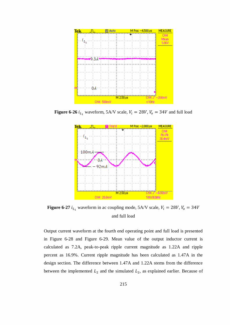
215
Figure 6-26 waveform, 5A/V scale, , and full load
Figure 6-27 waveform in ac coupling mode, 5A/V scale, ,
and full load
Output current waveform at the fourth end operating point and full load is presented
in Figure 6-28 and Figure 6-29. Mean value of the output inductor current is
calculated as 7.2A, peak-to-peak ripple current magnitude as 1.22A and ripple
percent as 16.9%. Current ripple magnitude has been calculated as 1.47A in the
design section. The difference between 1.47A and 1.22A stems from the difference
between the implemented and the simulated , as explained earlier. Because of
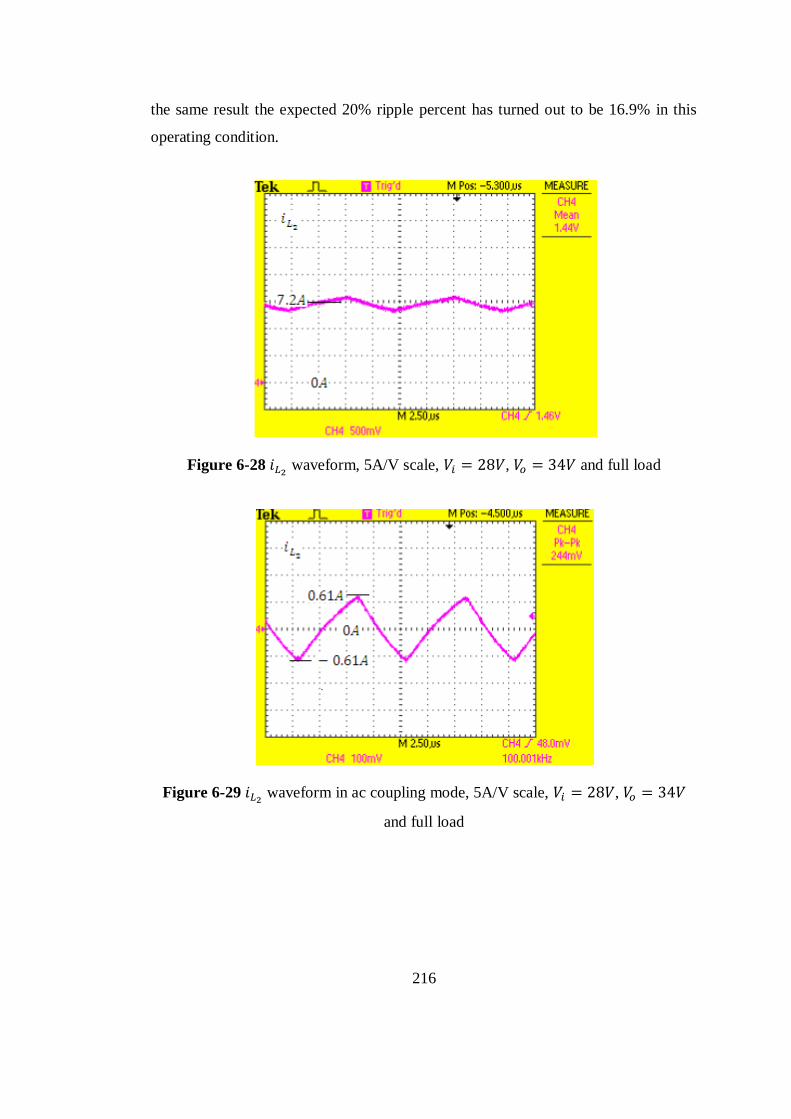
216
the same result the expected 20% ripple percent has turned out to be 16.9% in this
operating condition.
Figure 6-28 waveform, 5A/V scale, , and full load
Figure 6-29 waveform in ac coupling mode, 5A/V scale, ,
and full load

217
6.2.2.2.2 and
Waveforms at Half Load for the Fourth End
Operating Point
Input current waveform at the fourth end operating point and 50% load is presented
in Figure 6-30 and Figure 6-31. Mean value of the input inductor current is
calculated as 4.61A, peak-to-peak ripple as 0.184A and ripple percent as 4%. Note
that the ripple magnitude remains the same. Increase in the ripple percent is simply
caused by the decrease in the input current. The same arguments at full load case are
also valid here.
Figure 6-30 waveform, 5A/V scale, , and 50% load
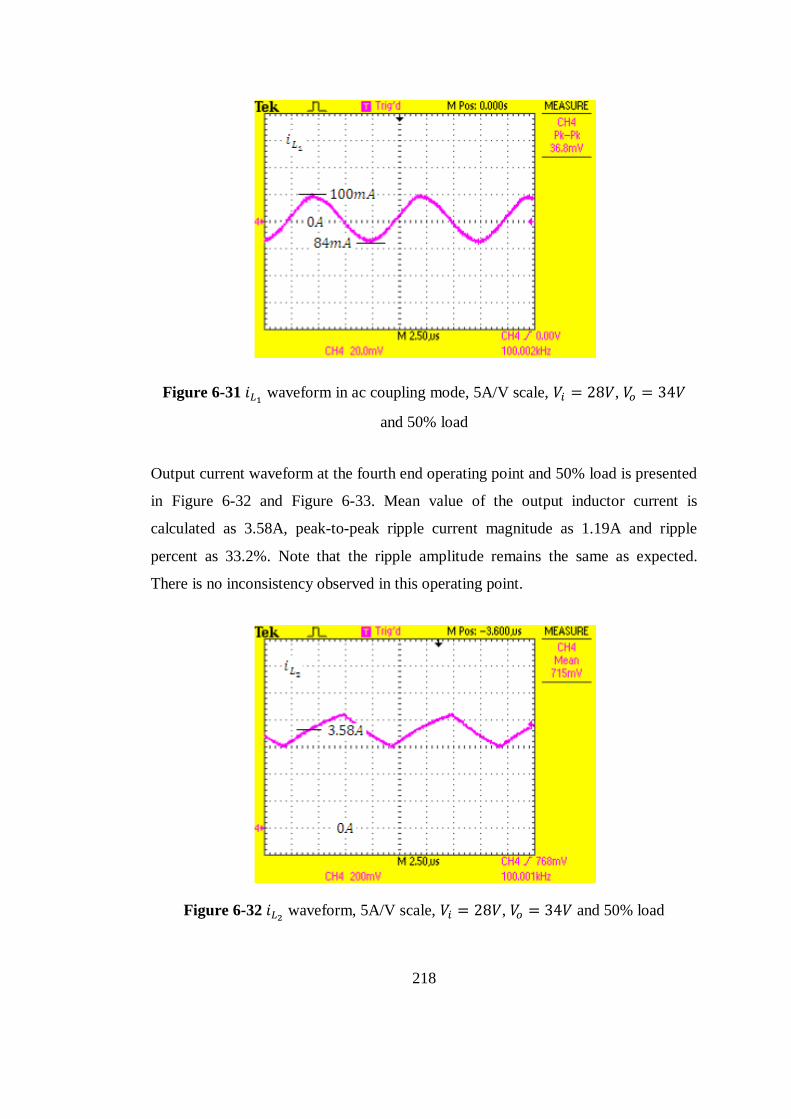
218
Figure 6-31 waveform in ac coupling mode, 5A/V scale, ,
and 50% load
Output current waveform at the fourth end operating point and 50% load is presented
in Figure 6-32 and Figure 6-33. Mean value of the output inductor current is
calculated as 3.58A, peak-to-peak ripple current magnitude as 1.19A and ripple
percent as 33.2%. Note that the ripple amplitude remains the same as expected.
There is no inconsistency observed in this operating point.
Figure 6-32 waveform, 5A/V scale, , and 50% load

219
Figure 6-33 waveform in ac coupling mode, 5A/V scale, ,
and 50% load
6.2.2.2.3 and
Waveforms at 10% Load for the Fourth End
Operating Point
Input current waveform at the fourth end operating point and 10% load is
presented in Figure 6-34 and Figure 6-35. Mean value of the input inductor current is
calculated as 0.98A, peak-to-peak ripple as 0.19A and ripple percent as 19.4%. Note
that the ripple magnitude remains the same. Increase in the ripple percent is simply
caused by the decrease in the mean value of the input current. The same arguments at
full load case are also valid here. From the input current waveforms at different load
levels in this end operating point, the following comment can be inferred: Ripple
current magnitudes at different load levels have turned out to be the same at this
operating point. Hence, there exists probably an unbalance between the inductors.
One can readjust the balance and get lower ripple percents. However, this time, the
balance between the inductors at other operating points is disturbed.
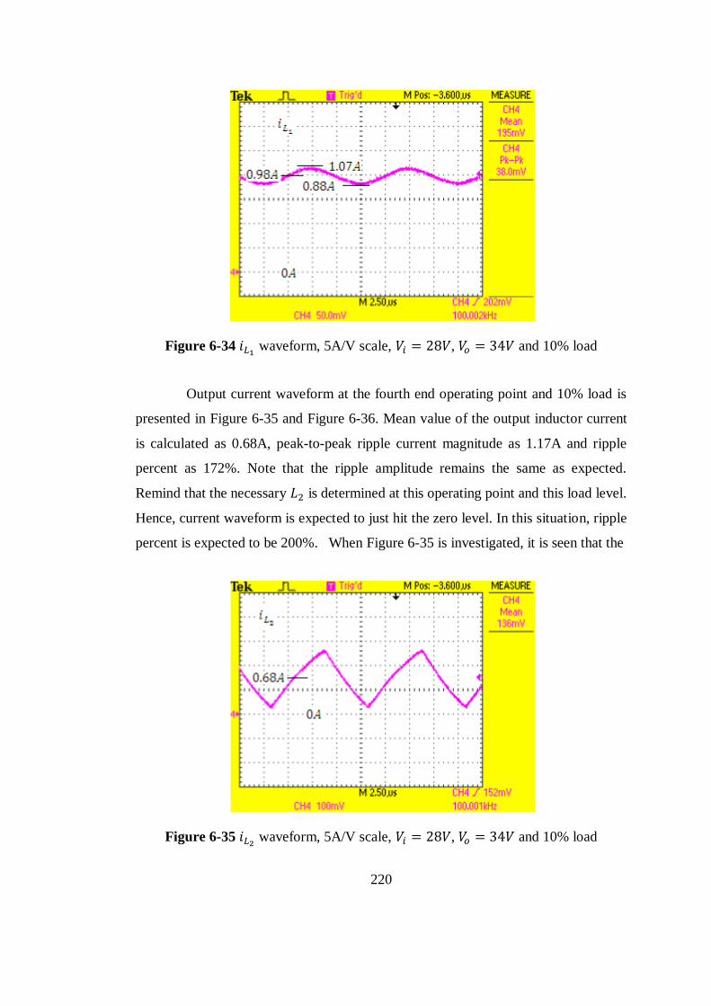
220
Figure 6-34 waveform, 5A/V scale, , and 10% load
Output current waveform at the fourth end operating point and 10% load is
presented in Figure 6-35 and Figure 6-36. Mean value of the output inductor current
is calculated as 0.68A, peak-to-peak ripple current magnitude as 1.17A and ripple
percent as 172%. Note that the ripple amplitude remains the same as expected.
Remind that the necessary is determined at this operating point and this load level.
Hence, current waveform is expected to just hit the zero level. In this situation, ripple
percent is expected to be 200%. When Figure 6-35 is investigated, it is seen that the
Figure 6-35 waveform, 5A/V scale, , and 10% load

221
Figure 6-36 waveform in ac coupling mode, 5A/V scale, ,
and 10% load
bottom of the waveform is a little bit higher than zero. This is due to the higher value
of implemented . To sum up, the results are consistent with the previous
simulations and calculations.
6.2.3 Efficiency of the Converter at Different Operating Conditions
In this section, measured efficiencies at the four end operating points and
three different load levels are presented. All information can be found in Table 6-1.
Input/output voltages are measured just at the input/output of the circuit. Input
current is read from the panel of the source and the output current from the panel of
the load, which are calibrated regularly. As it is seen in the table, the efficiency of the
converter decreases at low input voltage (i.e. high input current) and full load cases.
As explained in the design section, most of the power loss mechanisms are parasitic
resistances of the circuit elements. This kind of power losses increase with the square
of current magnitudes. Hence, at high current levels, decrease in efficiency is
expected. At low load, base power losses such as diode forward voltage drop may
dominate and decrease the efficiency. Generally, higher efficiencies are observed at
moderate power levels. These facts can be seen in Table 6-1.
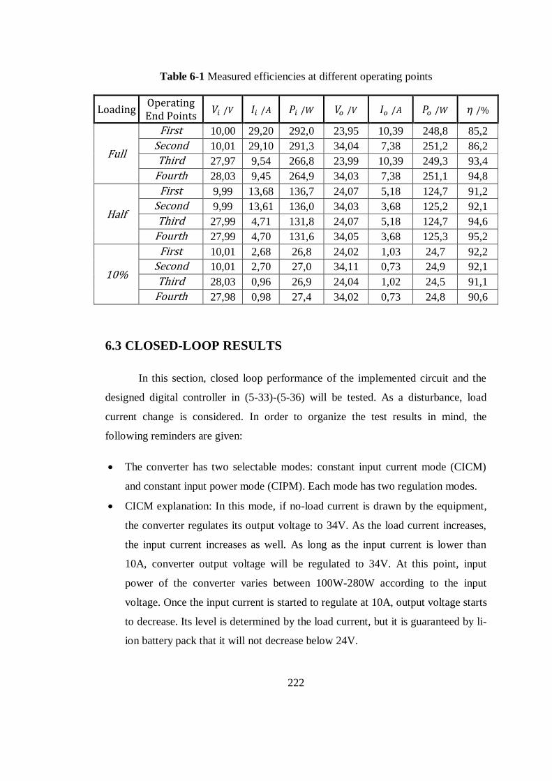
222
Table 6-1 Measured efficiencies at different operating points
Loading Operating End Points
Full
First 10,00 29,20 292,0 23,95 10,39 248,8 85,2
Second 10,01 29,10 291,3 34,04 7,38 251,2 86,2
Third 27,97 9,54 266,8 23,99 10,39 249,3 93,4
Fourth 28,03 9,45 264,9 34,03 7,38 251,1 94,8
Half
First 9,99 13,68 136,7 24,07 5,18 124,7 91,2
Second 9,99 13,61 136,0 34,03 3,68 125,2 92,1
Third 27,99 4,71 131,8 24,07 5,18 124,7 94,6
Fourth 27,99 4,70 131,6 34,05 3,68 125,3 95,2
10%
First 10,01 2,68 26,8 24,02 1,03 24,7 92,2
Second 10,01 2,70 27,0 34,11 0,73 24,9 92,1
Third 28,03 0,96 26,9 24,04 1,02 24,5 91,1
Fourth 27,98 0,98 27,4 34,02 0,73 24,8 90,6
6.3 CLOSED-LOOP RESULTS
In this section, closed loop performance of the implemented circuit and the
designed digital controller in (5-33)-(5-36) will be tested. As a disturbance, load
current change is considered. In order to organize the test results in mind, the
following reminders are given:
The converter has two selectable modes: constant input current mode (CICM)
and constant input power mode (CIPM). Each mode has two regulation modes.
CICM explanation: In this mode, if no-load current is drawn by the equipment,
the converter regulates its output voltage to 34V. As the load current increases,
the input current increases as well. As long as the input current is lower than
10A, converter output voltage will be regulated to 34V. At this point, input
power of the converter varies between 100W-280W according to the input
voltage. Once the input current is started to regulate at 10A, output voltage starts
to decrease. Its level is determined by the load current, but it is guaranteed by li-
ion battery pack that it will not decrease below 24V.
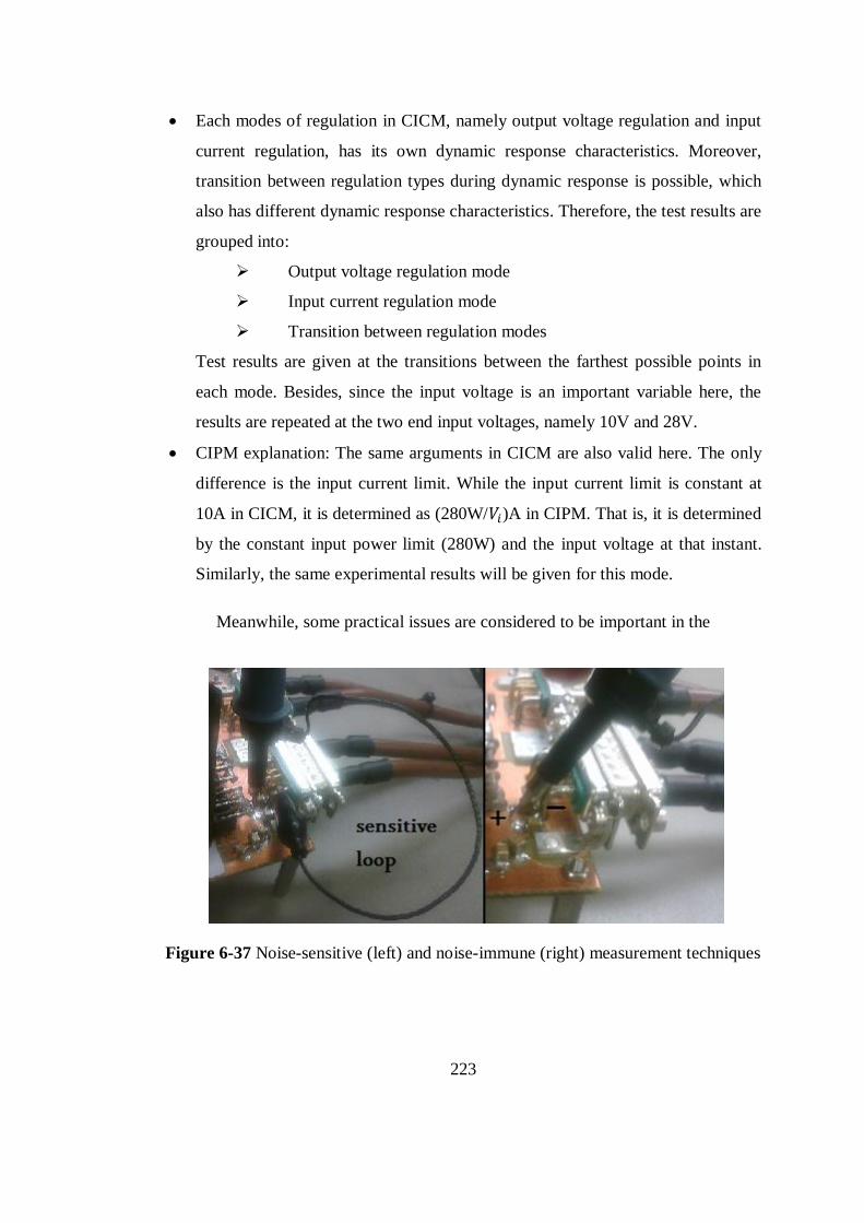
223
Each modes of regulation in CICM, namely output voltage regulation and input
current regulation, has its own dynamic response characteristics. Moreover,
transition between regulation types during dynamic response is possible, which
also has different dynamic response characteristics. Therefore, the test results are
grouped into:
Output voltage regulation mode
Input current regulation mode
Transition between regulation modes
Test results are given at the transitions between the farthest possible points in
each mode. Besides, since the input voltage is an important variable here, the
results are repeated at the two end input voltages, namely 10V and 28V.
CIPM explanation: The same arguments in CICM are also valid here. The only
difference is the input current limit. While the input current limit is constant at
10A in CICM, it is determined as (280W/ )A in CIPM. That is, it is determined
by the constant input power limit (280W) and the input voltage at that instant.
Similarly, the same experimental results will be given for this mode.
Meanwhile, some practical issues are considered to be important in the
Figure 6-37 Noise-sensitive (left) and noise-immune (right) measurement techniques
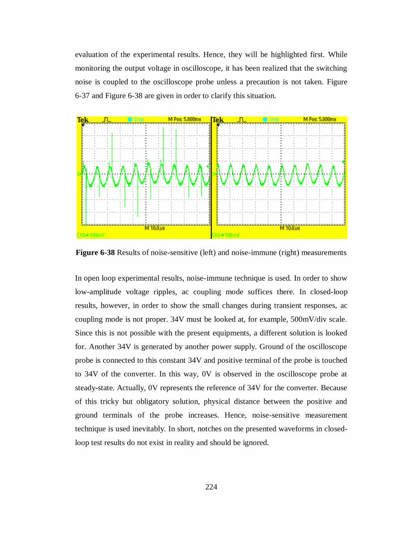
224
evaluation of the experimental results. Hence, they will be highlighted first. While
monitoring the output voltage in oscilloscope, it has been realized that the switching
noise is coupled to the oscilloscope probe unless a precaution is not taken. Figure
6-37 and Figure 6-38 are given in order to clarify this situation.
Figure 6-38 Results of noise-sensitive (left) and noise-immune (right) measurements
In open loop experimental results, noise-immune technique is used. In order to show
low-amplitude voltage ripples, ac coupling mode suffices there. In closed-loop
results, however, in order to show the small changes during transient responses, ac
coupling mode is not proper. 34V must be looked at, for example, 500mV/div scale.
Since this is not possible with the present equipments, a different solution is looked
for. Another 34V is generated by another power supply. Ground of the oscilloscope
probe is connected to this constant 34V and positive terminal of the probe is touched
to 34V of the converter. In this way, 0V is observed in the oscilloscope probe at
steady-state. Actually, 0V represents the reference of 34V for the converter. Because
of this tricky but obligatory solution, physical distance between the positive and
ground terminals of the probe increases. Hence, noise-sensitive measurement
technique is used inevitably. In short, notches on the presented waveforms in closed-
loop test results do not exist in reality and should be ignored.
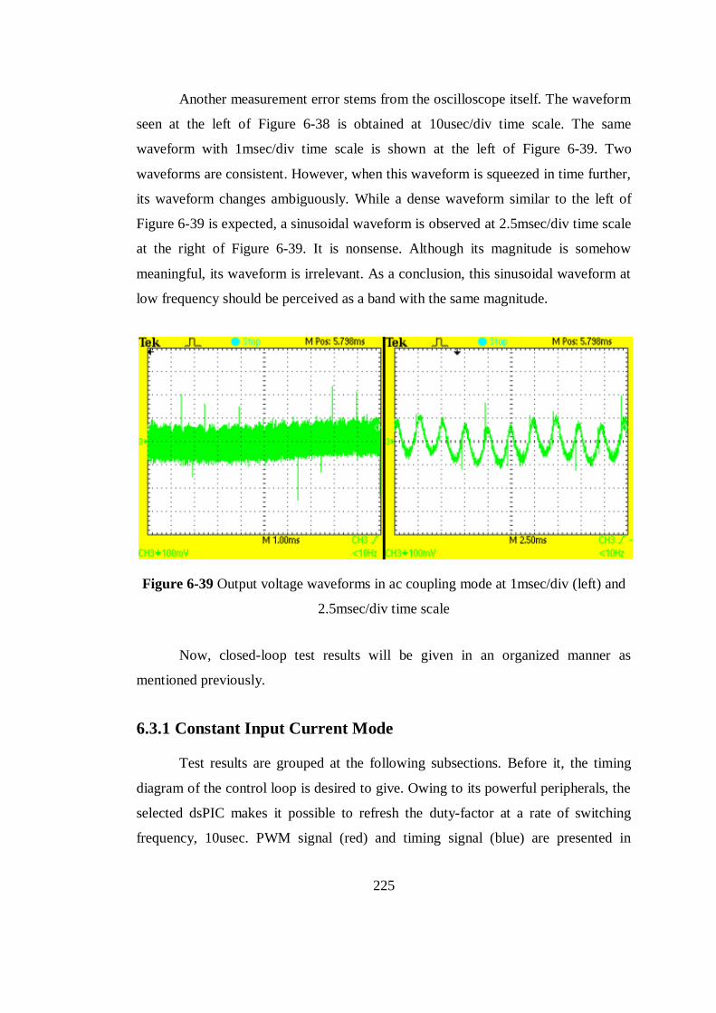
225
Another measurement error stems from the oscilloscope itself. The waveform
seen at the left of Figure 6-38 is obtained at 10usec/div time scale. The same
waveform with 1msec/div time scale is shown at the left of Figure 6-39. Two
waveforms are consistent. However, when this waveform is squeezed in time further,
its waveform changes ambiguously. While a dense waveform similar to the left of
Figure 6-39 is expected, a sinusoidal waveform is observed at 2.5msec/div time scale
at the right of Figure 6-39. It is nonsense. Although its magnitude is somehow
meaningful, its waveform is irrelevant. As a conclusion, this sinusoidal waveform at
low frequency should be perceived as a band with the same magnitude.
Figure 6-39 Output voltage waveforms in ac coupling mode at 1msec/div (left) and
2.5msec/div time scale
Now, closed-loop test results will be given in an organized manner as
mentioned previously.
6.3.1 Constant Input Current Mode
Test results are grouped at the following subsections. Before it, the timing
diagram of the control loop is desired to give. Owing to its powerful peripherals, the
selected dsPIC makes it possible to refresh the duty-factor at a rate of switching
frequency, 10usec. PWM signal (red) and timing signal (blue) are presented in
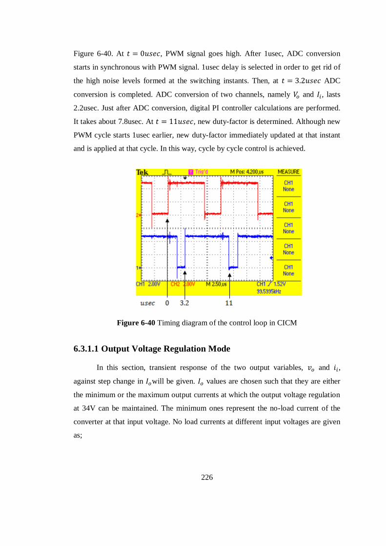
226
Figure 6-40. At , PWM signal goes high. After 1usec, ADC conversion
starts in synchronous with PWM signal. 1usec delay is selected in order to get rid of
the high noise levels formed at the switching instants. Then, at ADC
conversion is completed. ADC conversion of two channels, namely and , lasts
2.2usec. Just after ADC conversion, digital PI controller calculations are performed.
It takes about 7.8usec. At , new duty-factor is determined. Although new
PWM cycle starts 1usec earlier, new duty-factor immediately updated at that instant
and is applied at that cycle. In this way, cycle by cycle control is achieved.
Figure 6-40 Timing diagram of the control loop in CICM
6.3.1.1 Output Voltage Regulation Mode
In this section, transient response of the two output variables, and ,
against step change in will be given. values are chosen such that they are either
the minimum or the maximum output currents at which the output voltage regulation
at 34V can be maintained. The minimum ones represent the no-load current of the
converter at that input voltage. No load currents at different input voltages are given
as;

227
The maximum output currents represent the load currents at which the input current
rises to just below 10A.
From now on, red waveforms represent and green waveforms represent .
Besides, unless otherwise noted, current probe scale is at 5A/V. It will be at 50A/V
only at two groups of graphs, where the input current is high.
The parameters defining the performance of the transient response such as
rise time, settling time, maximum percent overshoot are not used regularly in these
test results. Because the regulated variable does not deviate much from its reference
value expect the exaggerated load current changes. In order to define these
parameters, a reference band of 2% or %5 is determined beforehand. Even if this
band is determined, these parameters may not carry sufficient information in some
graphs. Hence, instead of using these parameters, presenting raw data is considered
to be more meaningful in most case.
In Figure 6-41, the first snapshot is given. In order to get acquainted with
these graphs, some explanations will be presented here. The step load current change
from 0.1A to 2.6A occurs at the second time division from the left of the figures. It is
realized at the input voltage of 10V. At , is calculated as:
Similarly, at , is about 10A. At the left figure, the reference of is at
the bottom of the voltage divisions. The reference of is clearly seen by the pointer
2 (red) at the left of the figure. At the right figure, the reference of is brought to
zero, which is actually 34V as explained earlier with the name of tricky solution.
When changes, deviates at most 640mV from the reference. Note that this
deviation is within even 2% reference band, namely 680mV. In this situation,
settling time is regarded as zero. As an additional information, it takes about 15msec
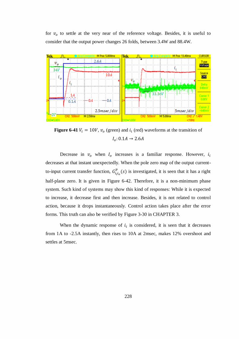
228
for to settle at the very near of the reference voltage. Besides, it is useful to
consider that the output power changes 26 folds, between 3.4W and 88.4W.
Figure 6-41 , (green) and (red) waveforms at the transition of
Decrease in when increases is a familiar response. However,
decreases at that instant unexpectedly. When the pole zero map of the output current-
to-input current transfer function,
is investigated, it is seen that it has a right
half-plane zero. It is given in Figure 6-42. Therefore, it is a non-minimum phase
system. Such kind of systems may show this kind of responses: While it is expected
to increase, it decrease first and then increase. Besides, it is not related to control
action, because it drops instantaneously. Control action takes place after the error
forms. This truth can also be verified by Figure 3-30 in CHAPTER 3.
When the dynamic response of is considered, it is seen that it decreases
from 1A to -2.5A instantly, then rises to 10A at 2msec, makes 12% overshoot and
settles at 5msec.
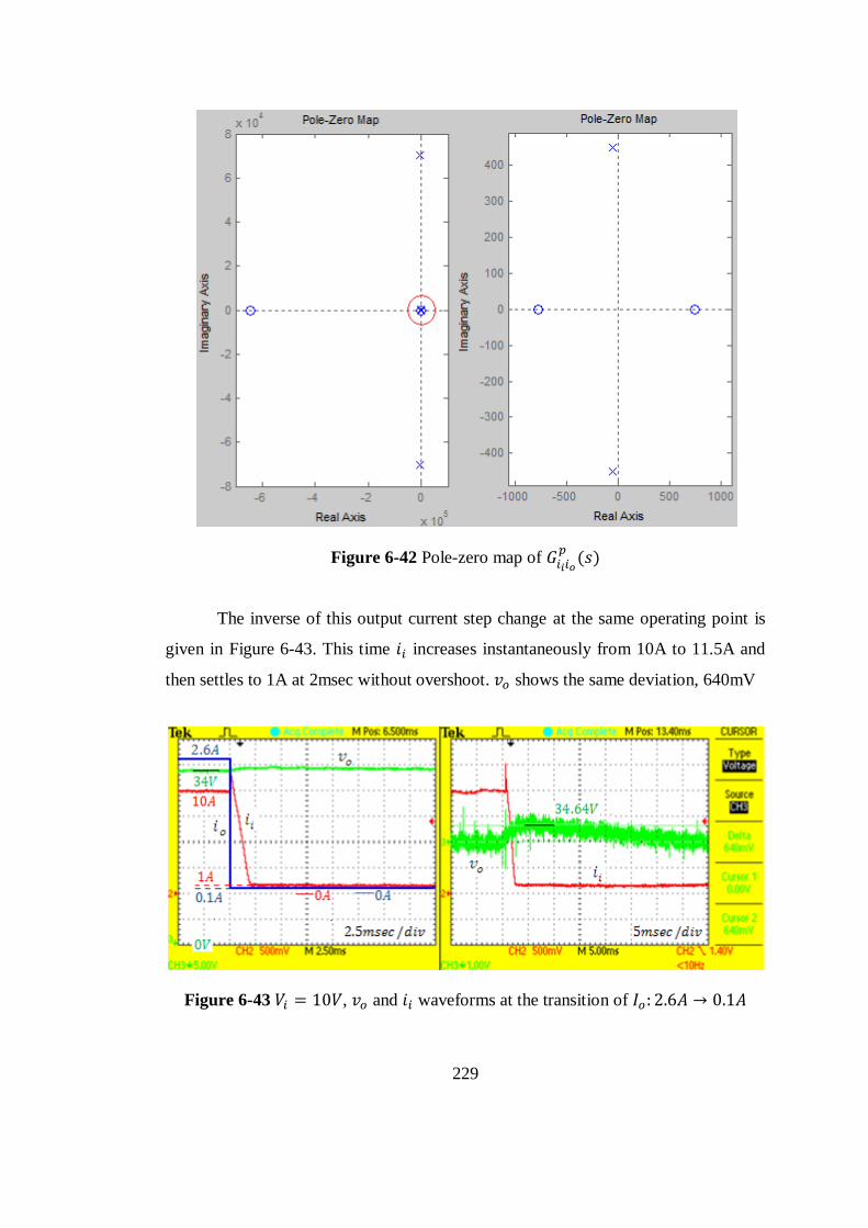
229
Figure 6-42 Pole-zero map of
The inverse of this output current step change at the same operating point is
given in Figure 6-43. This time increases instantaneously from 10A to 11.5A and
then settles to 1A at 2msec without overshoot. shows the same deviation, 640mV
Figure 6-43 , and waveforms at the transition of
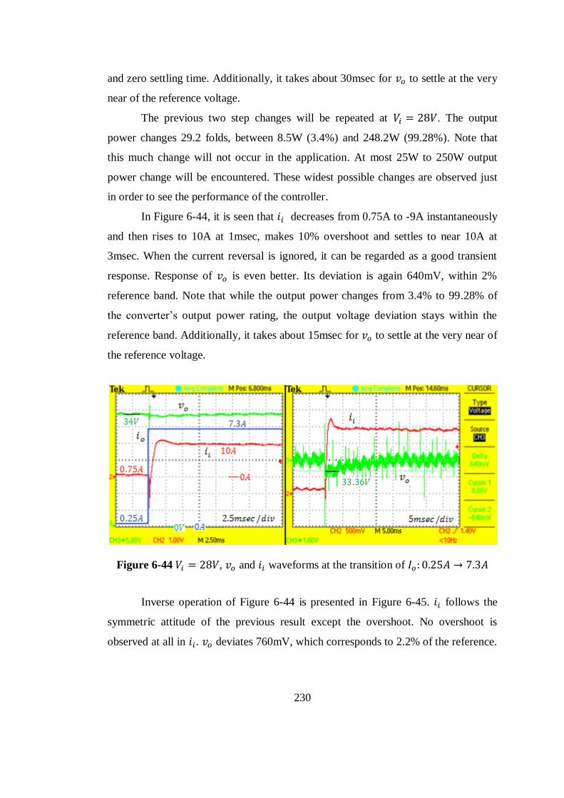
230
and zero settling time. Additionally, it takes about 30msec for to settle at the very
near of the reference voltage.
The previous two step changes will be repeated at . The output
power changes 29.2 folds, between 8.5W (3.4%) and 248.2W (99.28%). Note that
this much change will not occur in the application. At most 25W to 250W output
power change will be encountered. These widest possible changes are observed just
in order to see the performance of the controller.
In Figure 6-44, it is seen that decreases from 0.75A to -9A instantaneously
and then rises to 10A at 1msec, makes 10% overshoot and settles to near 10A at
3msec. When the current reversal is ignored, it can be regarded as a good transient
response. Response of is even better. Its deviation is again 640mV, within 2%
reference band. Note that while the output power changes from 3.4% to 99.28% of
the converter‟s output power rating, the output voltage deviation stays within the
reference band. Additionally, it takes about 15msec for to settle at the very near of
the reference voltage.
Figure 6-44 , and waveforms at the transition of
Inverse operation of Figure 6-44 is presented in Figure 6-45. follows the
symmetric attitude of the previous result except the overshoot. No overshoot is
observed at all in . deviates 760mV, which corresponds to 2.2% of the reference.

231
It enters within 2% reference band about 15msec and settles exactly to the reference
at about 40msec.
Figure 6-45 , and waveforms at the transition of
6.3.1.2 Input Current Regulation Mode
In this section, again, transient response of and against step change in
will be given. In input current regulation mode, is already limited to the current
limit, 10A. values in the following figures are determined accordingly: At the
lower , just rise to 10A and just decreases below 34V. At the higher , is
still 10A and decreases down to 24V. Besides, since and are constant, output
power almost does not change at all. According to , takes a value between 24V
and 34V. Actually, is not controlled in this mode. It is doing free fall. What is
controlled is .
In Figure 6-46, it is seen that when increases, starts to decrease from
just below 34V to just above 24V. Without control action, is expected to decrease
instantaneously (if non-minimum phase property is considered) and then increase
above 10A. However, it is decremented to 10A by control action. As shown in Figure
6-46, decreases from 10A to 9.2A instantly, then rises to 10.4A (4% overshoot)
and stays there until settles down to 24V. After reaches 24V, settles to 10A.
The same waveform is also observed in closed-loop simulations. Although the
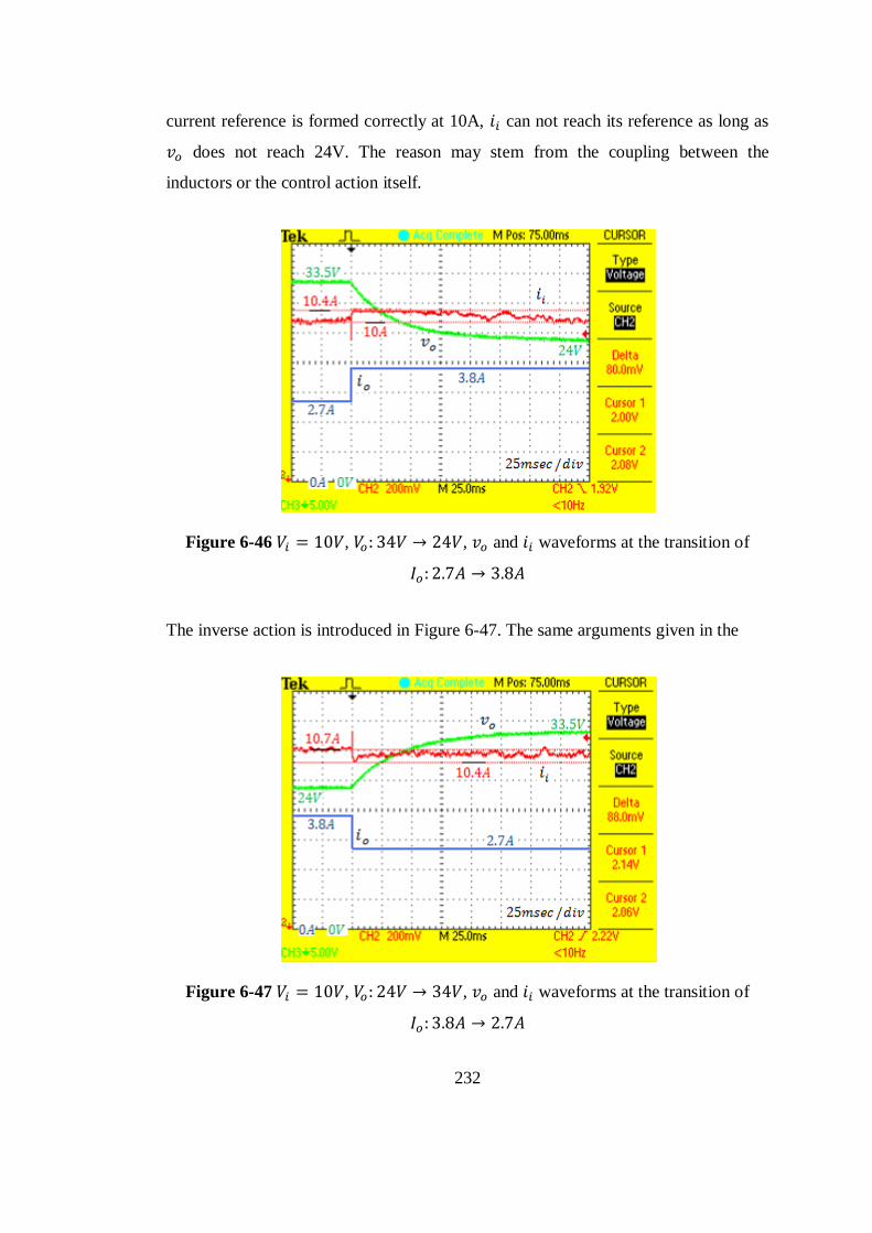
232
current reference is formed correctly at 10A, can not reach its reference as long as
does not reach 24V. The reason may stem from the coupling between the
inductors or the control action itself.
Figure 6-46 , , and waveforms at the transition of
The inverse action is introduced in Figure 6-47. The same arguments given in the
Figure 6-47 , , and waveforms at the transition of
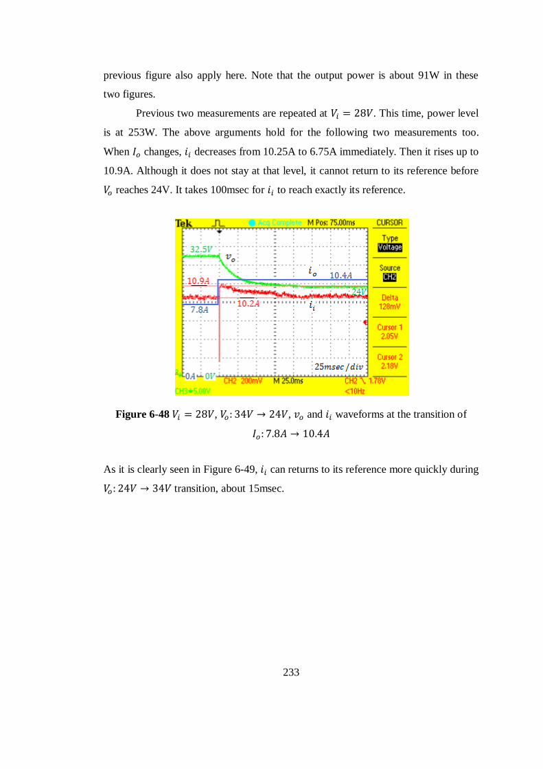
233
previous figure also apply here. Note that the output power is about 91W in these
two figures.
Previous two measurements are repeated at . This time, power level
is at 253W. The above arguments hold for the following two measurements too.
When changes, decreases from 10.25A to 6.75A immediately. Then it rises up to
10.9A. Although it does not stay at that level, it cannot return to its reference before
reaches 24V. It takes 100msec for to reach exactly its reference.
Figure 6-48 , , and waveforms at the transition of
As it is clearly seen in Figure 6-49, can returns to its reference more quickly during
transition, about 15msec.

234
Figure 6-49 , , and waveforms at the transition of
6.3.1.3 Transition between the Regulation Modes
In this section, the output current will be changed between no-load current
and the current at which the output voltage decreases down to its lower limit, 24V.
That is, will be changed between the farthest points among two regulation modes.
Therefore, regulation mode will change during these transitions. Different dynamic
responses are expected.
In Figure 6-50 and Figure 6-51, output power is changed stepwise between
3.4W (1.36%) and 129.2W (51.68%) at . When the load is increased,
increases to 10A at about 2 msec with a negligible overshoot. As expected, falls
down to 24V freely. When the load is decreased, wants to decrease after its instant
increase without control action. However, since is under its reference, is forced
to be 10A until reaches 34V. It can be observed in Figure 6-51. Most of 10A
drawn from the input is used to charge the energy transferring ( ) and output ( )
capacitor during 30msec. Then, decreases to 1A in 2.5msec. Also increases
from 24V to 34V in 30msec with 500mV overshoot, which is within 2% reference
band.
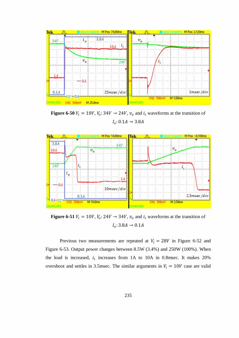
235
Figure 6-50 , , and waveforms at the transition of
Figure 6-51 , , and waveforms at the transition of
Previous two measurements are repeated at in Figure 6-52 and
Figure 6-53. Output power changes between 8.5W (3.4%) and 250W (100%). When
the load is increased, increases from 1A to 10A in 0.8msec. It makes 20%
overshoot and settles in 3.5msec. The similar arguments in case are valid
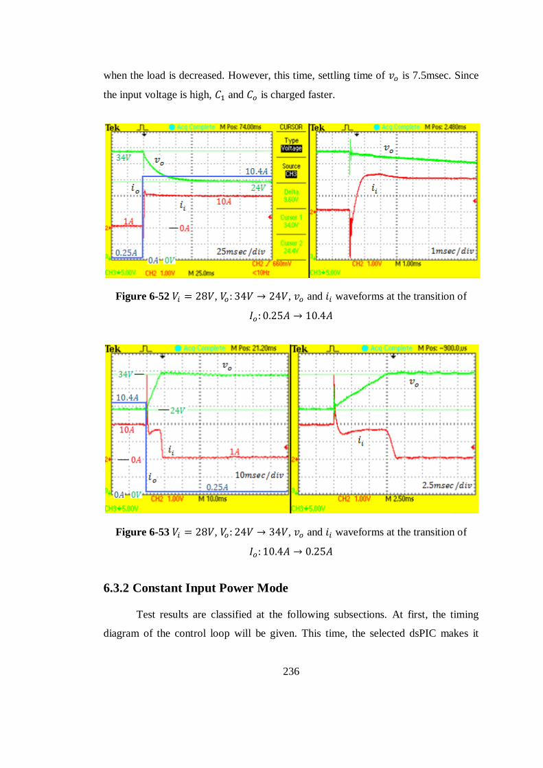
236
when the load is decreased. However, this time, settling time of is 7.5msec. Since
the input voltage is high, and is charged faster.
Figure 6-52 , , and waveforms at the transition of
Figure 6-53 , , and waveforms at the transition of
6.3.2 Constant Input Power Mode
Test results are classified at the following subsections. At first, the timing
diagram of the control loop will be given. This time, the selected dsPIC makes it
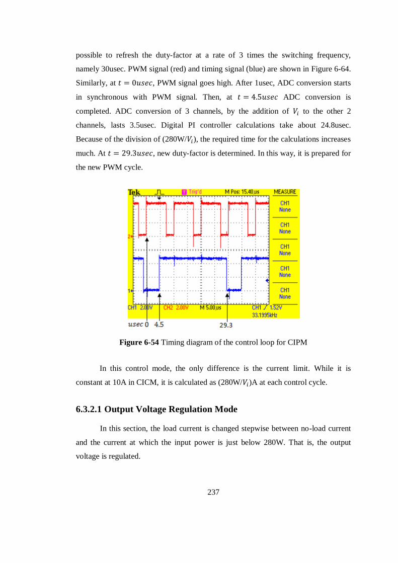
237
possible to refresh the duty-factor at a rate of 3 times the switching frequency,
namely 30usec. PWM signal (red) and timing signal (blue) are shown in Figure 6-64.
Similarly, at , PWM signal goes high. After 1usec, ADC conversion starts
in synchronous with PWM signal. Then, at ADC conversion is
completed. ADC conversion of 3 channels, by the addition of to the other 2
channels, lasts 3.5usec. Digital PI controller calculations take about 24.8usec.
Because of the division of (280W/ ), the required time for the calculations increases
much. At , new duty-factor is determined. In this way, it is prepared for
the new PWM cycle.
Figure 6-54 Timing diagram of the control loop for CIPM
In this control mode, the only difference is the current limit. While it is
constant at 10A in CICM, it is calculated as (280W/ )A at each control cycle.
6.3.2.1 Output Voltage Regulation Mode
In this section, the load current is changed stepwise between no-load current
and the current at which the input power is just below 280W. That is, the output
voltage is regulated.
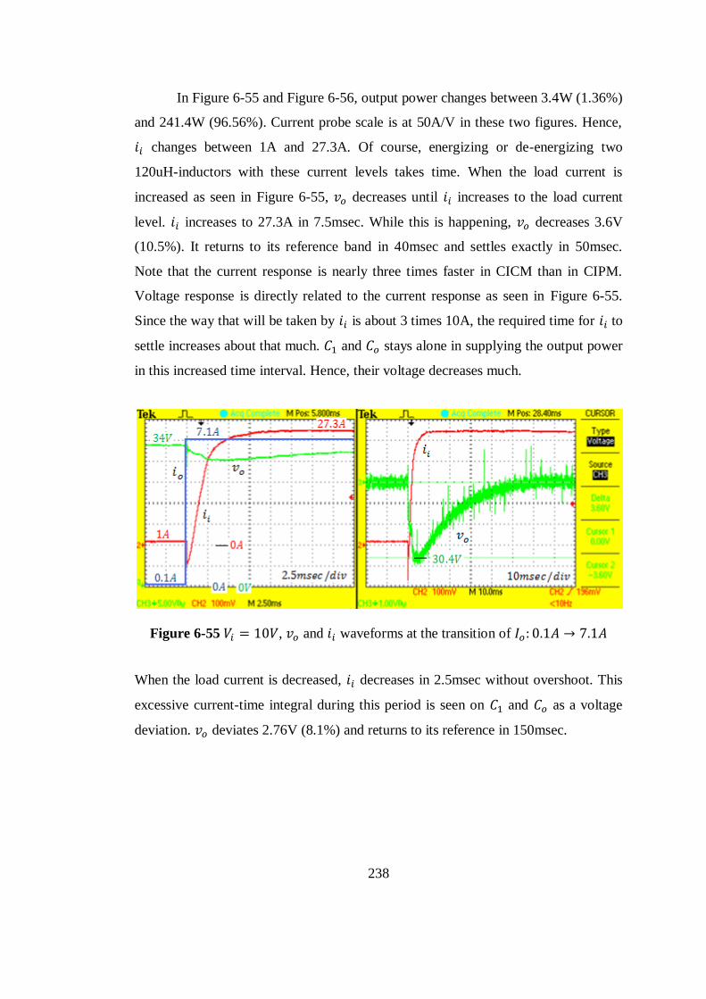
238
In Figure 6-55 and Figure 6-56, output power changes between 3.4W (1.36%)
and 241.4W (96.56%). Current probe scale is at 50A/V in these two figures. Hence,
changes between 1A and 27.3A. Of course, energizing or de-energizing two
120uH-inductors with these current levels takes time. When the load current is
increased as seen in Figure 6-55, decreases until increases to the load current
level. increases to 27.3A in 7.5msec. While this is happening, decreases 3.6V
(10.5%). It returns to its reference band in 40msec and settles exactly in 50msec.
Note that the current response is nearly three times faster in CICM than in CIPM.
Voltage response is directly related to the current response as seen in Figure 6-55.
Since the way that will be taken by is about 3 times 10A, the required time for to
settle increases about that much. and stays alone in supplying the output power
in this increased time interval. Hence, their voltage decreases much.
Figure 6-55 , and waveforms at the transition of
When the load current is decreased, decreases in 2.5msec without overshoot. This
excessive current-time integral during this period is seen on and as a voltage
deviation. deviates 2.76V (8.1%) and returns to its reference in 150msec.
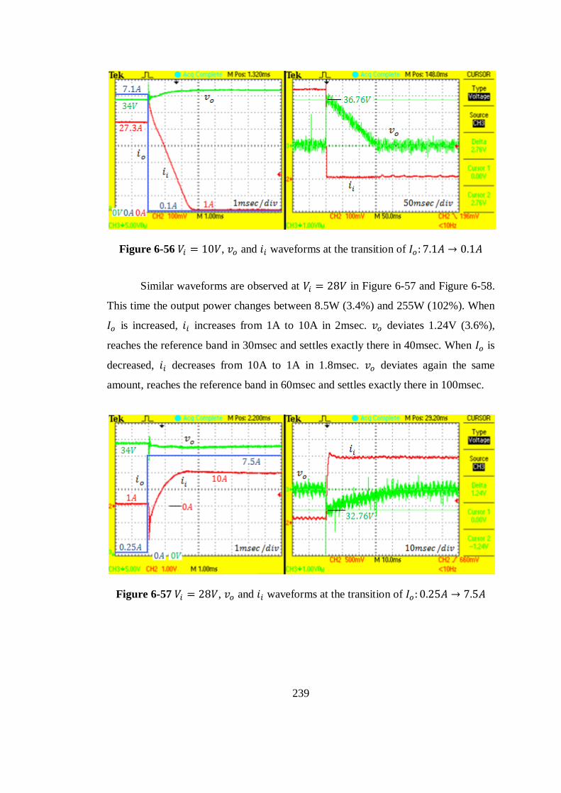
239
Figure 6-56 , and waveforms at the transition of
Similar waveforms are observed at in Figure 6-57 and Figure 6-58.
This time the output power changes between 8.5W (3.4%) and 255W (102%). When
is increased, increases from 1A to 10A in 2msec. deviates 1.24V (3.6%),
reaches the reference band in 30msec and settles exactly there in 40msec. When is
decreased, decreases from 10A to 1A in 1.8msec. deviates again the same
amount, reaches the reference band in 60msec and settles exactly there in 100msec.
Figure 6-57 , and waveforms at the transition of
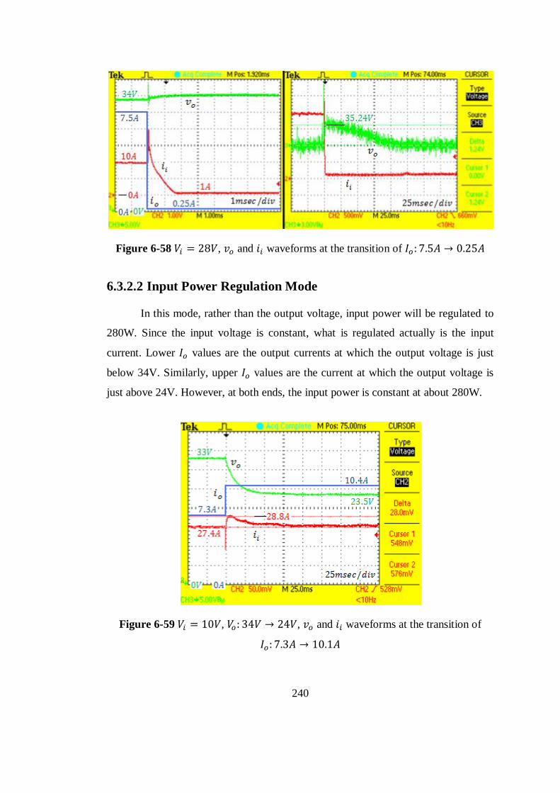
240
Figure 6-58 , and waveforms at the transition of
6.3.2.2 Input Power Regulation Mode
In this mode, rather than the output voltage, input power will be regulated to
280W. Since the input voltage is constant, what is regulated actually is the input
current. Lower values are the output currents at which the output voltage is just
below 34V. Similarly, upper values are the current at which the output voltage is
just above 24V. However, at both ends, the input power is constant at about 280W.
Figure 6-59 , , and waveforms at the transition of

241
In Figure 6-59 and Figure 6-60, current probe scale is 50A/V. Input power is
regulated to 274W. When is increased, deviates 1.4A (5.1%). It returns to its
reference band in 32msec and settles exactly in 75msec. When is decreased,
deviates 1.6A (6.1%). It has the same timing values. Note that Figure 6-59 and
Figure 6-60 are highly symmetrical.
Figure 6-60 , , and waveforms at the transition of
In Figure 6-61 and Figure 6-62, the previous measurements are repeated at
. Input power is again regulated to 274W. When is increased, deviates
0.8A (8%). It returns to its reference band in 40msec and settles exactly in 50msec.
When is decreased, deviates 1A (10%). It has the same timing values. Again,
Figure 6-61 and Figure 6-62 are highly symmetrical. In these four figures, it is
observed that cannot settle until reaches its stable point.
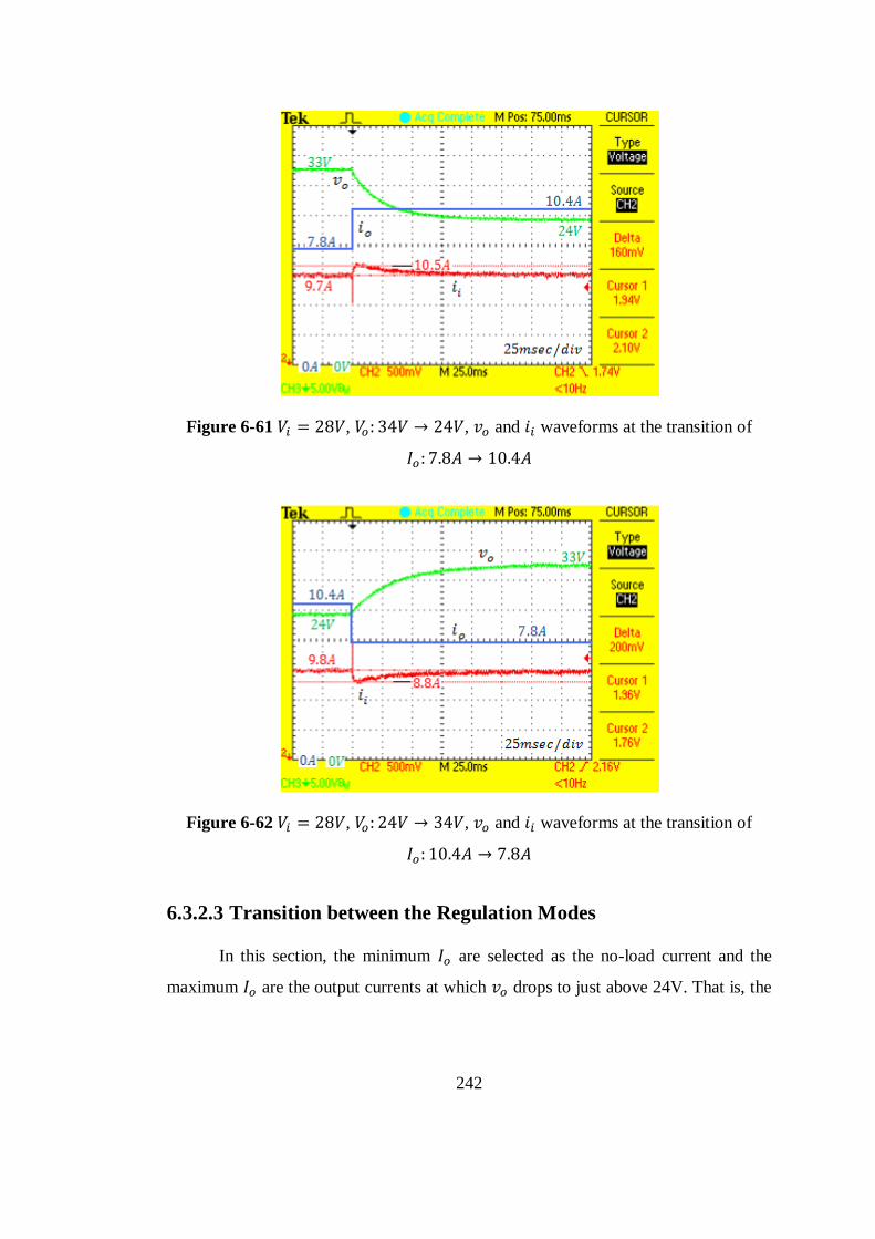
242
Figure 6-61 , , and waveforms at the transition of
Figure 6-62 , , and waveforms at the transition of
6.3.2.3 Transition between the Regulation Modes
In this section, the minimum are selected as the no-load current and the
maximum are the output currents at which drops to just above 24V. That is, the
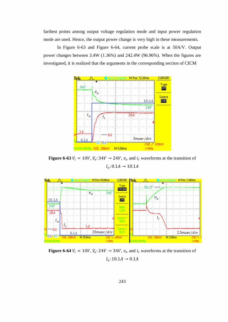
243
farthest points among output voltage regulation mode and input power regulation
mode are used. Hence, the output power change is very high in these measurements.
In Figure 6-63 and Figure 6-64, current probe scale is at 50A/V. Output
power changes between 3.4W (1.36%) and 242.4W (96.96%). When the figures are
investigated, it is realized that the arguments in the corresponding section of CICM
Figure 6-63 , , and waveforms at the transition of
Figure 6-64 , , and waveforms at the transition of
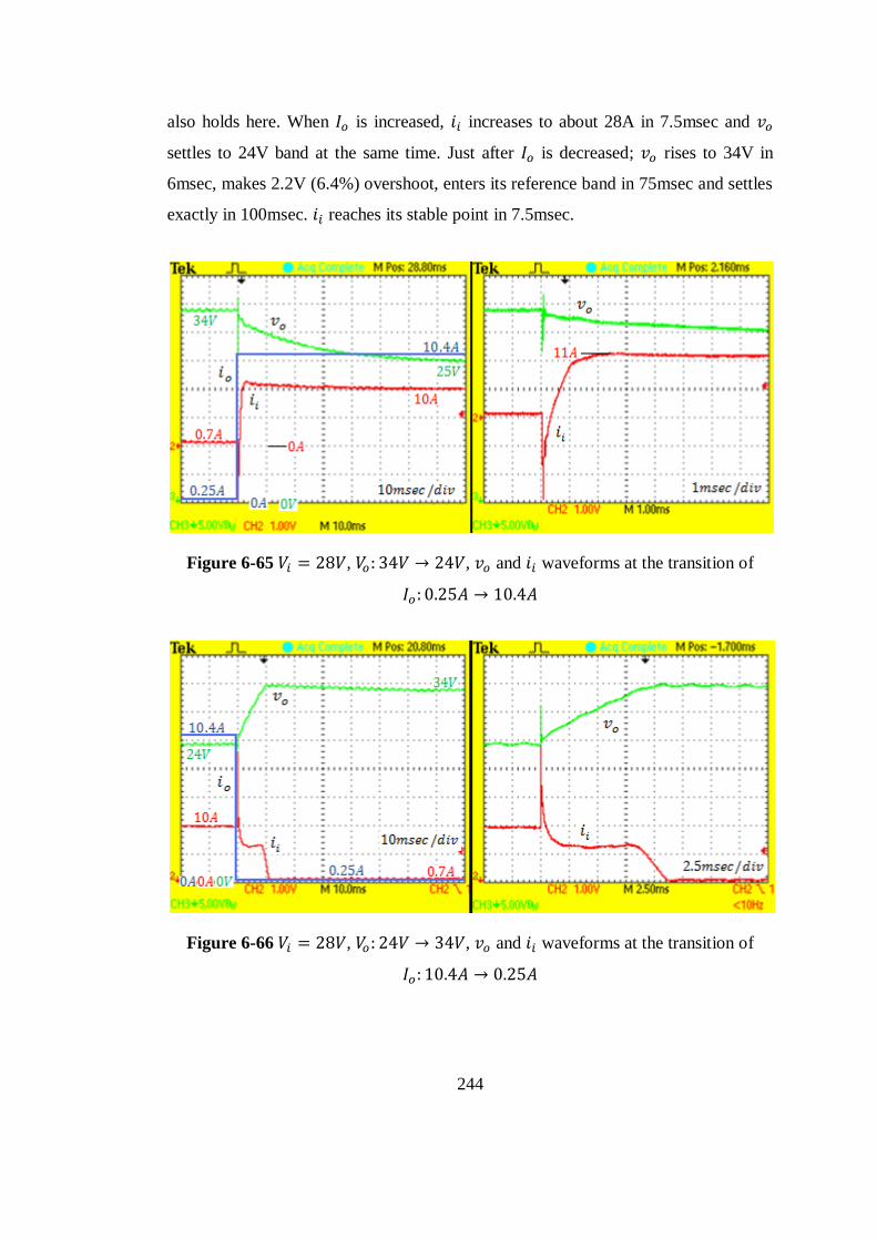
244
also holds here. When is increased, increases to about 28A in 7.5msec and
settles to 24V band at the same time. Just after is decreased; rises to 34V in
6msec, makes 2.2V (6.4%) overshoot, enters its reference band in 75msec and settles
exactly in 100msec. reaches its stable point in 7.5msec.
Figure 6-65 , , and waveforms at the transition of
Figure 6-66 , , and waveforms at the transition of

245
When the same transitions are repeated at , Figure 6-65 and Figure
6-66 are obtained. Output power changes between 8.5W (3.4%) and 249.6W
(99.84%). When is increased; increases to about 10A in 1.3msec, makes 15%
overshoot. It settles exactly when settles to 24V. When is decreased; rises to
34V in 8.5msec, makes 0.8V (2.3%) overshoot, enters its reference band in 25msec
and settles exactly in 50msec. reaches its stable point in 11.2msec.

246
CHAPTER 7
SUMMARY AND CONCLUSIONS
It has been observed that despite the presence of the parasitic elements and
many practical problems in the implementation of the coupled-inductor Šuk
converter, satisfactory results are obtained in terms of voltage and current
waveforms. Besides, in design process, in order to provide coupling condition, an
adjustment inductor is added to one of the inductors. Šuk has preferred to adjust the
air gap in order to provide coupling. Since it necessitates very sensitive positioning
and seems to be not practical, a more practical approach, namely adjustment inductor
method, is suggested and verified by the simulations and implementation. Utilization
of this method eases the implementation very much.
Implementation of integrated magnetic Šuk converter is considered to be
troublesome because there are two airgaps to be positioned sensitively in that case.
Moreover, they are not independent. Hence, an iterative positioning must be
performed during the circuit is operating. As Šuk has suggested, iteration goes on
until the ripple-free input and output currents are obtained. Following the application
of adjustment inductor method to coupled-inductor, it is realized that the same
method can also be applied to integrated magnetic structure. The balance between
and is provided by adding an adjustment inductor to and ripple-free input
current waveform can be obtained. Similarly, the balance between and is
provided by adding an adjustment inductor to and ripple-free output current

247
waveform can be reached. In this way, it is not struggled with dependency and
sensitive positioning of the cores. Note that this approach is not validated for
integrated magnetic structure and it is given just as a proposal for future works.
In theory, it is expected to get ripple-free input current waveforms at each
operating point for the implemented circuit. In practice, however, due to the parasitic
and nonlinear characteristics of the circuit elements, getting ripple-free input current
waveform is expected to deteriorate to some extent. In the implemented circuit, this
fact is observed. While a ripple percent well below 1% is obtained in one operating
point, 2% ripple percent is reached at another operating point at the same load level.
This low degradation may be regarded as the success in selection of the core material
and type. Recall that the B-H curve of the selected core plays an important role in the
deterioration of the ripple-free current waveform property with respect to the
operating conditions.
In the implemented circuit, voltage overshoots turn out to be much lower than
as expected. Since the switched current can be at most 40A, serious voltage
overshoots are expected in the beginning. Therefore, use of RC snubber circuits are
planned in order to limit the voltage overshoots on the switch and the diode. During
layout process, much attention is paid to minimize the parasitic inductances of the
paths where pulsating current pass. As a result, voltage overshoots turns out to be
low and snubber circuits are not used.
The efficiency of the implemented converter can be regarded as high when
the voltage, current and power levels are considered. Note that hard switching is
utilized in the implemented circuit. Using this switching method, further increases in
efficiencies are not possible. Šuk has brought a solution to this problem and
suggested Šuk converter versions which are utilizing soft switching technique. In
this way, switching losses are eliminated and only conduction losses remains.
Moreover, since the switching frequency can be increased, dimensions of the filter
elements (i.e. capacitors and inductors) decrease dramatically. As a result, more
efficient and compact converter is obtained. For future work, soft switching versions
of the Šuk converter are strictly recommended. Detailed information about them can
be found in [28, 32, 33].

248
In obtaining the transfer functions of the circuit, state-space averaging method
has been used and it has given accurate results. Most of the time, a simpler method is
used in the derivation of transfer functions of switching circuit. In that method, the
circuit is generally divided into a switching structure, an isolation transformer (if it
exists) and L-C output filter. Since a coupled-inductor has been utilized in the circuit,
this division could not be accomplished and therefore that technique has not been
realized. It is observed that state-space averaging method gives very accurate results
in this type of extraordinary situations. It also lets the parasitic elements of the
switching structure and the isolation transformer be included in the transfer
functions. In the simple method, however, only the parasitic elements of the output
L-C filter can be included.
In the control of the implemented circuit, some theoretical problems are
encountered. Since the circuit has four energy storing elements with two inductors
and two capacitors, the order of the denominator of the transfer functions turns out to
be four. This order is two in most of the circuit topologies, which comes from the
output L-C filter. Therefore, many of the widely known control approaches for the
switching converters are not applicable. This may not be regarded as a problem. The
real problem is that some transfer functions have zeros with positive real parts. These
kinds of systems are called non-minimum phase systems and exhibits unfamiliar
responses. Moreover, these systems are known to be hard to control and have slower
dynamic responses with respect to minimum phase systems. These facts have been
faced with during simulating and implementing the control of the circuit. For
example, when voltage mode control was applied, the output voltage oscillated
continuously. The use of current mode control has solved this problem. Besides,
when the response times of the circuit are investigated, it may be argued that the
system responds slowly. Trying to decrease the response times is possible by
modifying the controller functions. However, doing so makes the output variables
oscillates. As a consequence, the converter has to responds slowly in order to be
stable and not to be oscillatory.
At the beginning, there are not any dynamic response specifications for the
implemented circuit. Therefore, the circuit is designed according to steady-state

249
specifications such as current and voltage ripples on the elements. When the dynamic
response of the circuit is to be improved, it is realized that the poles and zeros of the
derived transfer functions do not permit such an improvement. The locations of the
poles and zeros depend on the parameters of the circuit elements. Hence, improving
the dynamic response necessitates redesign of the circuit. As a result, the following
conclusion is reached for future works: If the dynamic response of the converter is
important for a particular application, the dynamic response specifications must be
considered in the design phase of the circuit and in the selection phase of the circuit
components. For example, for a little improvement in steady-state response, one may
select a larger energy storing element. However, this may result in a much more
degradation in dynamic response.
250
REFERENCES
[1]: Slobodan Šuk, “Modelling, Analysis, and Design of Switching Converters”,
Ph.D. thesis, California Institute of Technology, November 1976
[2]: Zekiye Günaydın, “Analysis and Design of a Šuk Switching Regulator”, M.Sc.
thesis, Middle East Technical University, May 2009
[3]: R.D.Middlebrook and S.Šuk, “A General Unified Approach to Modelling
Switching-Converter Power Stages”, Proceedings of the IEEE Power
Electronics Specialists Conference, Cleveland, OH, June 1976
[4]: W.M.Polivka, P.R.K.Chetty and R.D.Middlebrook, “State-Space Average
Modelling of Converters with Parasitic and Storage-Time Modulation”, In
Proceedings of the IEEE Power Electronics Specialists Conference, Atlanta,
GA, June 1980
[5]: Slobodan Šuk, “Basics of Switched-Mode Power Conversion: Topologies,
Magnetics, and Control”, Advances in Switched-Mode Power Conversion
Volumes I and II, pp. 279-310, TESLAco, Pasadena, CA, July 1983
[6]: Slobodan Šuk and R.D.Middlebrook, “A New Optimum Topology Switching
DC-to-DC Converter”, Proceedings of the IEEE Power Electronics Specialists
Conference, Palo Alto, CA, June 1977

251
[7]: Slobodan Šuk and R.D.Middlebrook, “Coupled-Inductor Extension of a New
Optimum Topology Switching DC-to-DC Converter”, Proceedings of the IEEE
Industry Applications Society Annual Meeting, Los Angeles, CA, October 1977
[8]: Slobodan Šuk, “Switching DC-to-DC Converter with Zero Input or Output
Current Ripple”, Proceedings of the IEEE Industry Applications Society Annual
Meeting, Toronto, ONT, October 1978
[9]: L.Rensink, A.Brown, S.P.Hsu and S.Šuk, “Design of a Kilowatt Off-Line
Switcher Using a Šuk Converter”, Proceedings of the Sixth National Solid-State
Power Conversion Conference, Miami Beach, FL, May 1979
[10]: Slobodan Šuk, “A New Zero-Ripple Switching DC-to-DC Converter and
Integrated Magnetics”, Proceedings of the IEEE Power Electronics Specialists
Conference, Atlanta, GA, June 1980
[11]: Slobodan Šuk and R.D.Middlebrook, “Advances in Switched-Mode Power
Conversion Part I”, Robotics Age, Vol. 1, No. 2, pp. 6-19, Winter 1979
[12]: Slobodan Šuk and R.D.Middlebrook, “Advances in Switched-Mode Power
Conversion Part II”, Robotics Age, Vol. 2, No. 2, pp. 28-41, Summer 1980
[13]: Slobodan Šuk, “New Magnetic Structures for Switching Converters”, IEEE
Transactions on Magnetics, Vol. MAG-19, No. 2, pp. 75-83, March 1983
[14]: R.D.Middlebrook, “Generalized Theory of Switching DC-to-DC Converters”,
Proceedings of Region 6 Conference, Anaheim, CA, February 1982
[15]: Alan Cocconi and Slobodan Šuk, “Design of a 2kW, 100kHz Switching
Regulator for Space Shuttle”, Proceedings of the Fifth International PCI’82,
Geneva, Switzerland, September 1982

252
[16]: S.Šuk and William M.Polivka, “Analysis of Integrated Magnetics to Eliminate
Current Ripple in Switching Converters”, Proceedings of the Sixth
International PCI’83, Orlando, FL, April 1983
[17]: S.Šuk and John F. Brewer, “Low Noise, Low Cost 150W Off-Line Switcher”,
Powerconversion International Magazine, Vol. 9, No. 4, April 1983
[18]: R.D.Middlebrook, “Design Considerations and Noise Reduction in Switching
Converters”, Powerconversion International Magazine, 1983
[19]: Keyue M.Smedley and S.Šuk, “Dynamics of One-Cycle Controlled Šuk
Converters”, IEEE Transactions on Power Electronics, Vol. 10, No. 6,
November 1995
[20]: J.Mahdavi, A.Emadi and H.A.Toliyat, “Application of State Space Averaging
Method to Sliding Mode Control of PWM DC/DC Converters”, IEEE Industry
Applications Society Annual Meeting, New Orleans, Louisiana, October 1997
[21]: C.K.Tse and William C.Y.Chan, “Instability and Chaos in a Current-Mode
Controlled Šuk Converter”, Hong Kong Polytechnic University, 1995
[22]: Enrico Santi and S.Šuk, “Modelling of One-Cycle Controlled Switching
Converters”, California Institute of Technology, 1992
[23]: Vatché Vorpérian, “The Effect of the Magnetizing Inductance on the Small-
Signal Dynamics of the Isolated Šuk Converter”, IEEE Transactions on
Aerospace and Electronic Systems, Vol. 2, No. 3, July 1996
[24]: Robert W.Erickson and D.Maksimoviš, “Fundamentals of Power Electronics”,
Second Edition, Kluwer Academic Publishers, Massachusetts, January 2004

253
[25]: Philip T.Krein, “Elements of Power Electronics”, Oxford University Press,
Oxford, New York, 1998
[26]: Slobodan Šuk and R.D.Middlebrook, “DC-to-DC Switching Converter”,
United States Patent, No. 4,184,197, January 1980
[27]: Enrico Santi, Aliso Viejo and S.Šuk, “Low Profile Coupled Inductors and
Integrated Magnetics”, United States Patent, No. 5,790,005, August 1998
[28]: Slobodan Šuk, “Lossless Switching DC to DC Converter with DC
Transformer”, United States Patent, No. 6,400,579 B2, June 2002
[29]: “Magnetic Core Characteristics”, Texas Instruments, 2001
[30]: “SIFERRIT Material N27”, Epcos, September 2006
[31]: “PM 74/59 Core and Accessories”, Epcos, September 2006
[32]: Slobodan Šuk, “Lossless Switching Converter with DC Transformer”, United
States Patent, No. 6,388,896, May 2002
[33]: Slobodan Šuk, “Lossless Switching DC-to-DC Converter”, United States
Patent, No. 6,462,962, October 2002


![Modeling and Control of a Multi-stage Interleaved …by Cuk in buck-boost converter [6], [7]. In [8], Witulski has shown how a coupled inductor´ differs from normal inductor and transformer](https://img.dokumen.tips/doc/110x75/5f4d972268593756d475e471/modeling-and-control-of-a-multi-stage-interleaved-by-cuk-in-buck-boost-converter.jpg)


![A Coupled Inductor Based Single Stage High Gain …...2018/05/10 · Shafeeq[16] 4 4 1 1 1 2 0 2 2 More number of switches and more conduction loss. Coupled inductor topologies Yris[17]](https://img.dokumen.tips/doc/110x75/5fe1d31c00785e1917778dbe/a-coupled-inductor-based-single-stage-high-gain-20180510-shafeeq16-4.jpg)