Embed Size (px)
Citation preview

Design and Implementation of a Plesiochronous Multi-Core 4x4 Network-on-Chip Platform
with MPI HAL Support
Wajid Hassan Minhass
Stockholm 2009
Department of Electronic, Computer and Software Systems School of Information and Communication Technology
Royal Institute of Technology (KTH) Sweden
This thesis is submitted to the Royal Institute of Technology in partial fulfillment of the requirements for the degree of Master of Science
________________________________________________________________________ii
Supervisor
Dr. Johnny Öberg
Department of Electronic, Computer and Software Systems School of Information and Communication Technology
Royal Institute of Technology (KTH)
Examiner
Dr. Ingo Sander Department of Electronic, Computer and Software Systems
School of Information and Communication Technology Royal Institute of Technology (KTH)
Minhass, Wajid Hassan
Design and Implementation of Plesiochronous Multi-Core 4x4 Network-on-Chip Platform with MPI HAL Support
TRITA-ICT-EX-2009:13 ISBN 978-91-7415-376-7

________________________________________________________________________iii
Abstract Due to the rapid advancements in technology scaling in the last decade or so, multiprocessor system-on-chip design (MPSoC) is becoming a regular feature of the embedded systems. Multiple system cores require simultaneous usage of communication resources thus causing a sharp increase in the bandwidth demand. Although the shared-bus system holds many advantages, yet it does not scale. Hence in the recent years, improvements in both architecture and protocol of the interconnect subsystem have been introduced. The network on chip (NoC) architecture builds upon improvements in the current shared-bus communication system. In addition to offering a promising solution to the scalability problem by enhancing the topology design, NoC also brings a whole new innovation to the on-chip interconnect system in the form of packet-based communication paradigm. However, the practical implementation of NoC is not yet fully mature and a lot of open challenges still remain. The aim of this project is to design and implement a 2-D mesh 4x4 multi-core NoC-platform using multiple FPGA (field programmable gate array) boards. The platform can later be utilized for testing and verifying a variety of techniques e.g. fault tolerance protocol design to deal with broken links etc. In addition to exploring the NoC design field, an inter-board communication protocol has also been designed and implemented. Four FPGA boards are connected together to form the 4x4 NoC platform, with each FPGA device hosting a Quad-Core NoC. The NoC platform is plesiochronous since the FPGA boards operate on a similar but not identical clock speed. Asynchronous clock bridges have been utilized to resolve the communication synchronization and meta-stability issues. Since the FPGA board I/O pins are limited, the solution has been focused on building a narrower interconnect while keeping the system scalable. The NoC-based system has been designed and implemented using Altera Stratix II FPGA boards. Each switch has been connected to a separate single resource through a resource network interface. In order to facilitate system design and verification, soft embedded processor cores have been chosen as the resource in this case. Keeping the communication paradigm in view, a hardware abstraction layer (HAL) based on the MPI (message passing interface) library routines has also been developed. Absolute addressing scheme is utilized for the nodes, together with the usage of dimension-order routing protocol. Keywords: NoC, MPSoC, Multi-core, Plesiochronous, MPI, Source-Synchronous, hardware platform, Clock Domain Bridges

________________________________________________________________________iv

________________________________________________________________________v
Preface This thesis is submitted in partial fulfillment of the requirements for the degree of Master of Science at the Royal Institute of Technology (KTH), Sweden. Its content is based on the work carried out in the Department of Electronic, Computer and Software Systems at the School of Information and Communication Technology (ICT – KTH). With a duration of 20 weeks, the thesis corresponds to a credit of 30 ECTS points. Successful completion of a work of this kind requires the coordinated efforts of many individuals. I would like to start off by sending out a resounding thanks to my supervisor Dr. Johnny Öberg for his exceptional guidance, invaluable close involvement with the work and seemingly boundless patience. His ability to always find time to discuss the various issues encountered, and to discuss them in the most amicable manner, contributed dearly in the successful completion of the thesis work. I am thankful to Dr. Ingo Sander, the examiner, for his generous discussions, encouragement and help when required. I would also like to thank all of my colleagues, especially Naveed Ahmed, who were with me at the time when this thesis work was initiated as a Design Project. The discussions carried out at that time helped me immensely in developing a much deeper understanding of the work. Since this thesis also marks the end of my MS studies, I would also like to express my gratitude to KTH for providing me an opportunity to learn from the best in the field. I really had a wonderfully memorable time here in Sweden. Special thanks to the Higher Education Commission (HEC), Pakistan for sponsoring my MS studies. Finally, I wish to extend my grand and deepest gratitude to my parents and family for their continuous support and encouragement which served as a driving force throughout the course of work.
Wajid Hassan Minhass Department of Electronic, Computer and Software Systems
School of Information and Communication Technology Royal Institute of Technology (KTH), Sweden
June 1, 2009

________________________________________________________________________vi

________________________________________________________________________vii
Contents Abstract............................................................................................................................. iii Preface................................................................................................................................ v List of Figures................................................................................................................... ix 1. Introduction................................................................................................................... 1
1.1 Network-on-Chip (NoC)..................................................................................... 1 1.2 Objectives ........................................................................................................... 2 1.3 Outline................................................................................................................. 3
2. NoC Platform - Introduction ....................................................................................... 5
2.1 NoC – Basic Concepts ........................................................................................ 5 2.2 4x4 NoC – Top View.......................................................................................... 7 2.3 Target Hardware Platform .................................................................................. 8
3. Inter-Board Communication ..................................................................................... 11
3.1 Clock Domain Translation Protocol ................................................................. 11 3.2 Target Platform Limitations.............................................................................. 12 3.3 Board-Bridge Unit (BBU)................................................................................. 13 3.4 Problems discovered during implementation.................................................... 16
4. RNI and Switch ........................................................................................................... 19
4.1 Standard Quad-Core NoC - Overview.............................................................. 19 4.2 Resource Network Interface (RNI)................................................................... 21
4.2.1 RNI – Device Drivers ............................................................................... 22 4.2.2 RNI - Switch Communication .................................................................. 23
4.3 Switch ............................................................................................................... 23 4.3.1 Routing Management................................................................................ 23 4.3.2 Switch Interfaces....................................................................................... 24 4.3.3 Switch Architecture .................................................................................. 26
5. Hardware Abstraction Layer..................................................................................... 29
5.1 Message Passing Interface (MPI) ..................................................................... 29 5.2 Supported MPI-Routines .................................................................................. 31 5.3 Message Transfer Protocol ............................................................................... 33
________________________________________________________________________viii
6. Demonstration and Evaluation.................................................................................. 37 6.1 Game of Life (GoL) .......................................................................................... 37
6.1.1 Background............................................................................................... 37 6.1.2 Implementation ......................................................................................... 38 6.1.3 Problems encountered during implementation ......................................... 42
6.2 Lamp-Light Method.......................................................................................... 43 6.3 System Specifications ....................................................................................... 44
7. Conclusions and Future Work................................................................................... 47 References........................................................................................................................ 49 A. List of Abbreviations ................................................................................................. 51 B. Cable Configuration................................................................................................... 53 C. Programming the Flash Memory ............................................................................. 55

________________________________________________________________________ix
List of Figures Figure 1.1: Moore's Law – Intel Processors ....................................................................... 1 Figure 2.1: A mesh NoC with 9 Nodes............................................................................... 6 Figure 2.2: 4x4 NoC Design – Top View........................................................................... 7 Figure 2.3: Flit Format........................................................................................................ 7 Figure 2.4: Packet Format................................................................................................... 8 Figure 2.5: Nios Development Board ................................................................................. 8 Figure 2.6: Design Arrangement......................................................................................... 9 Figure 3.1: Two-Flop Synchronizer.................................................................................. 11 Figure 3.2: Single Board I/O requirement ........................................................................ 12 Figure 3.3: Cable Configuration ....................................................................................... 13 Figure 3.4: A 2x4 NoC...................................................................................................... 13 Figure 3.5: Board Bridge Unit – the Sufficient Model ..................................................... 14 Figure 3.6: Board Bridge Unit - Final Model ................................................................... 14 Figure 3.7: BBU Arrangement on the 4x4 NoC ............................................................... 15 Figure 3.8: Serial Communication Protocol ..................................................................... 15 Figure 4.1: System Level diagram of the Standard Quad-Core NoC ............................... 19 Figure 4.2: Top Level Design Diagram ............................................................................ 20 Figure 4.3: Snapshot of the SOPC Builder design............................................................ 20 Figure 4.4: RNI Memory Configuration........................................................................... 21 Figure 4.5: RNI receive memory channels ....................................................................... 22 Figure 4.6: Flit Format...................................................................................................... 23 Figure 4.7: Switch - Board-Bridge Unit Interface ............................................................ 24 Figure 4.8: BBU-ILU communication protocol................................................................ 25 Figure 4.9: Switch Architecture........................................................................................ 26 Figure 4.10: Arbitration Logic - Internal Architecture ..................................................... 27 Figure 5.1: System HAL - Top view ................................................................................ 29 Figure 5.2: Eager vs Rendezvous Protocol ....................................................................... 31 Figure 5.3: MPI Initialization Routine.............................................................................. 31 Figure 5.4: MPI Standard Send Routine ........................................................................... 32 Figure 5.5: MPI Standard Receive Routine ...................................................................... 32 Figure 5.6: MPI PID-based Send Routine ........................................................................ 33 Figure 5.7: MPI PID-based Receive Routine ................................................................... 33 Figure 5.8: Message transfer from resource 1 to resource 2............................................. 34 Figure 5.9: Command Register ......................................................................................... 34 Figure 5.10: Setup Flit ...................................................................................................... 34 Figure 5.11: RNI Control Register.................................................................................... 34

________________________________________________________________________x
Figure 6.1: Still Life and Spaceship patterns .................................................................... 38 Figure 6.2 Oscillator Patterns ........................................................................................... 38 Figure 6.3: GoL Implementation – Bottom-Up Sweep .................................................... 39 Figure 6.4: GoL Implementation - Top-Down Sweep...................................................... 40 Figure 6.5: The NoC platform .......................................................................................... 42 Figure 6.6: Lamp-Light Method ....................................................................................... 43 Figure B.1: PROTO2 Expansion Prototype Connector - J15, J16, and J17 ..................... 53 Figure B.2: Cable Arrangement........................................................................................ 53

Chapter 1
Introduction This chapter introduces the concept of Network-on-Chip (NoC) based on the current challenges in the System-on-Chip (SoC) design domain. In addition, the objectives of the thesis are also highlighted and then an overview of the remaining portions of the thesis report is presented.
1.1 Network-on-Chip (NoC) Advancements in the System-on-Chip (SoC) technology are one of the major contributors to the rapidly evolving micro-electronic products. These products in return cause a dramatic change in our everyday life. Though the advancements may seem uniform and even, yet there are still a lot of challenges that the SoC design methodologies have to overcome in order to ensure that they match the advancement in the integration technology. According to Moore’s law proposed in 1965, the number of gates on a chip double every 18 months thus raising the complexity of the chip to a whole new level [1]. In line with this, the logic capacity of a single chip has increased exponentially over time as shown in Figure 1.1.
Figure 1.1: Moore's Law – Intel Processors [2]

________________________________________________________________________2
Today, this has enabled the designers to place a large number of resources on a single chip; in turn creating a huge bandwidth demand. Traditionally, shared-bus based on-chip communication systems (simple or hierarchical) have been the priority option. But with such an immense increase in bandwidth demand, the bus based system has limited benefits to offer as it lacks the ability to scale in parallel with the chip capacity. Not only does it lack the concurrent communication capability but at the same time, it is inefficient in terms of energy consumption as every bus based transaction is carried out in terms of a broadcast. Network-on-Chip (NoC) offers a plausible solution to the scalability problem [3]. Compared to the bus system, the NoC architecture is far more reusable and is based on a systematic approach which suggests scalable global communication. By introducing the packet based communication paradigm to the on-chip communication domain, NoC has given a completely new outlook in designing solutions to address the interconnect fabric design issues [4]. For instance, the wire lengths can now be controlled by matching the physical constraints to the network topology. Similarly, the communication bottlenecks created in the traditional interconnect systems, when a large number of resources are placed along them, is also effectively dealt with in the NoC architecture design. Since a NoC can be of an arbitrary size, the bandwidth can be boosted by simply increasing the number of switches and the number of links [5]. These novel capabilities place the NoC architecture among one of the most promising solutions to the current SoC design interconnect challenges.
1.2 Objectives Although advantages of the NoC architecture have been widely discussed, the practical implementation of NoC is not yet fully mature and a lot of open challenges still remain. Due to high cost, manufacturability and verification issues in ASIC; prototyping the designs on FPGAs has become a widely popular option. The main objective is to design and implement a multi-core 4x4 NoC-platform using multiple FPGA (field programmable gate array) boards. The project builds on the previous 2x2 Quad-Core NoC designed by Dr. Johnny Öberg [6]. This design would be referred to as the ‘base Quad-Core NoC’ in the following chapters. The compulsory goals of the project are:
• Design and implement a 4x4 NoC Platform using four Altera Stratix II Boards • The design should have the following features:
o 5-port switch (router) o Bi-sync FIFO or similar design for inter-board communication o MPI like hardware abstraction layer (HAL). o Delivery of packet measurable in HAL for upper layers of software.
• Game of Life is to be used for the demonstration of the 4x4 NoC platform. On- board LEDs should be used for general demonstration.
• A console based application (connected to one of the nodes) should also be implemented. It should demonstrate the successful inter-node communication and provide the user with the following performance figures:
o Worst case packet delivery time.

________________________________________________________________________3
o Best case packet delivery time. o Average case of packet delivery time.
The following areas will also be explored optionally, provided that the compulsory goals are completed earlier:
• Upgrade RNI by incorporating a scheme for re-ordering the packet flits received out of sequence due to misrouting
• Upgrade the system to a 6x6 NoC platform with identical features • Design and implement a 7–port switch for 3D NoC Design • Strategy on dealing with broken links • Plug-and-play strategies
The system can later be utilized as a platform for testing and verification of a variety of techniques e.g. fault tolerance protocol design for dealing with broken links etc.
1.3 Outline The contents of the upcoming chapters are summarized as follows: Chapter 2 presents an overview of the NoC platform. It starts off by presenting some basic NoC concepts, followed up by the top-level details of the NoC platform. The target hardware platform is also introduced. NoC platform design arrangement with respect to the target hardware is also discussed. Chapter 3 describes the inter-board communication. Detailed overview of the inter-board communication protocol design and implementation is provided. This chapter also covers the details of the impacts that the target hardware platform limitations have on the inter-board communication. Chapter 4 presents the Resource Network Interface (RNI) and the switch. It starts off with a brief overview of the standard Quad-Core NoC design. Later parts of the chapter cover the thorough details of the RNI and the switch. The routing management part is also covered in the switch details. Chapter 5 is dedicated to covering the HAL (Hardware Abstraction Layer). Detailed description of the supported MPI library routines is provided here. Chapter 6 describes the demonstration and evaluation details of the NoC platform. Details of both the Game of Life and the Lamp-Light method have been provided. The chapter also gives out the performance figures extracted from the NoC platform. The report is summed up by presenting the conclusions and the future work options in Chapter 7.

________________________________________________________________________4

________________________________________________________________________5
Chapter 2
NoC Platform - Introduction This chapter presents an overview of the NoC platform. Some basic NoC concepts have been discussed at the beginning. Then the top-level details of the 4x4 NoC platform are described as an introduction. The target hardware platform is also discussed later, together with its limitations.
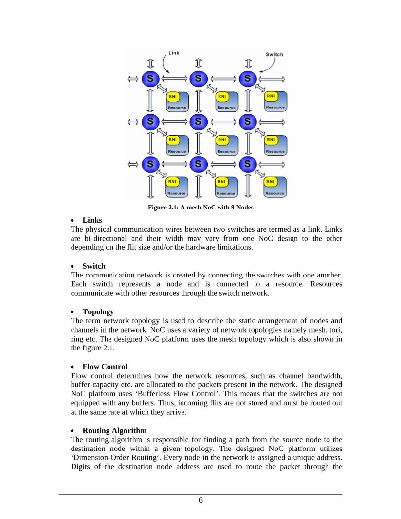
2.1 NoC – Basic Concepts The NoC architecture is based on a network of switches connected together through physical links. Many topologies exist for the switch interconnection. Mesh topology (as shown in Figure 2.1) is the simplest and most commonly used. Each switch is connected to a resource. The resources are equipped with a Resource-Network-Interface (RNI) in order to communicate with the switches. The communication is done by routing packets over the network instead of driving dedicated wires. A NoC can be described best by its topology, routing protocol, arbitration algorithm and the switching technique. In the implemented NoC platform (4x4 Mesh NoC), each node is mapped to a single resource. In order to facilitate system design and verification, soft embedded processor cores (Altera® Nios® II processors) have been chosen as resources. Figure 2.1 shows a mesh NoC-based system with 9 nodes as a reference. Different concepts of the NoC architecture are briefly described below:
• Resource A resource is the unit that is connected to the switch. It can be a processor, memory, IP block, FPGA, ASIC, or a bus-based sub-system. In the designed NoC platform, all resources are chosen to be Nios II soft processors with 10K of embedded memory. • Resource Network Interface (RNI) The resource network interface (RNI) is used to connect the resource to the rest of the network through the switch. The main purpose of the RNI is to translate the communication protocol used by the resource into the network communication protocol. Thus RNI is responsible for translation, message fragmentation, packet formatting, packet flits reordering and any other specific requirement that may be set by the resource communication interface.
________________________________________________________________________6
Figure 2.1: A mesh NoC with 9 Nodes
• Links The physical communication wires between two switches are termed as a link. Links are bi-directional and their width may vary from one NoC design to the other depending on the flit size and/or the hardware limitations. • Switch The communication network is created by connecting the switches with one another. Each switch represents a node and is connected to a resource. Resources communicate with other resources through the switch network. • Topology The term network topology is used to describe the static arrangement of nodes and channels in the network. NoC uses a variety of network topologies namely mesh, tori, ring etc. The designed NoC platform uses the mesh topology which is also shown in the figure 2.1. • Flow Control Flow control determines how the network resources, such as channel bandwidth, buffer capacity etc. are allocated to the packets present in the network. The designed NoC platform uses ‘Bufferless Flow Control’. This means that the switches are not equipped with any buffers. Thus, incoming flits are not stored and must be routed out at the same rate at which they arrive.
• Routing Algorithm The routing algorithm is responsible for finding a path from the source node to the destination node within a given topology. The designed NoC platform utilizes ‘Dimension-Order Routing’. Every node in the network is assigned a unique address. Digits of the destination node address are used to route the packet through the

________________________________________________________________________7
network. The packet is routed along (+x, -x, +y, -y) until it reaches its destination. The designed NoC platform uses a y-before-x routing algorithm.
2.2 4x4 NoC – Top View The NoC platform has a total of 16 nodes connected in a mesh network. Figure 2.2 shows the top view of the 4x4 NoC design. Node Address Configuration Every node has been assigned a specific node ID keeping in view its row-column position in the overall design. As shown, the node IDs have been assigned using a 4-bit frame, 2 bits for the row position and 2 bits for the column position. The node in the lower left corner has row 0 and column 0; thus has been given the ID ’00,00’ (row,col). These node IDs have been used as a routing decision base. In every node, its own ID is hard coded enabling it to recognize packets sent to itself and also to make routing decisions accordingly.
Figure 2.2: 4x4 NoC Design – Top View
Flit and Packet Format The flit format is shown in the figure 2.3. As shown, the flit has 52 bits in total, out of which 32 bits are reserved for the payload.
Figure 2.3: Flit Format

________________________________________________________________________8
The packet format is shown in figure 2.4. Every outgoing packet has two additional flits at the beginning: a setup flit followed by a flit carrying the global time stamp. Setup flit contains the packet related information required by the receiver for successful packet reception. The global time stamp is reserved for the future use as a debugging feature. The remaining flits are all data flits. The maximum number of flits in a packet is decided by the system buffer size. The designed output system buffer can currently hold up to 128 flits, thus a maximum of 126 data flits can be sent out in any packet.
Figure 2.4: Packet Format
2.3 Target Hardware Platform The Nios development board of Altera, StratixTM II edition, has been used as the hardware platform in order to develop the Multiprocessor NoC system.
Figure 2.5: Nios Development Board [7]

________________________________________________________________________9
The board is equipped with a Stratix II EP2S60 FPGA device which has 24,176 adaptive logic modules (ALMs) and 1.3 million bits of on-chip memory. In addition, the platform also holds 16 Mbytes of flash memory, 1 Mbyte of static RAM and 16 Mbytes of SDRAM [7]. The platform is equipped with a 50 MHz oscillator and zero-skew clock distribution circuitry. Nios II soft embedded processors are used as resources in the multiprocessor NoC design. Nios II are general purpose RISC processors specifically designed for the Altera family of FPGAs. Primarily, Quartus II®, Nios II IDE®, SOPC Builder®, Altera Debug Client® and ModelSim® are the tools used during the development work. Design Arrangement Keeping in view the size of the target FPGA, design space requirement of the base Quad-Core NoC and the possible future upgrades; the 4x4 NoC has been arranged onto four separate FPGA devices. Since the target hardware platform, the Nios Development Board, holds only one FPGA device thus four Nios Development Boards have been used for developing the NoC platform. Figure 2.6 shows the design division together with the board IDs.
Figure 2.6: Design Arrangement
All the Nios Development Boards operate at 50 MHz. Since every board has its own clock source, so they can be stated as operating at almost the same frequency with unknown difference in phases i.e. they are plesiochronous with respect to each other. Special inter-board communication units have been designed to take care of the synchronization and metastability issues encountered when dealing with multiple clock domains. Chapter 3 covers the inter-board communication in more detail.

________________________________________________________________________10

________________________________________________________________________11
Chapter 3
Inter-Board Communication Stable inter-board communication is vital for successful operation of the NoC platform. This chapter provides the details of the technique utilized to overcome the metastability and synchronization issues while performing an inter-board packet transfer. Limitations of the target hardware platform and their impact on the design are also discussed.
3.1 Clock Domain Translation Protocol Since all the boards are being fed by different clock sources, the inter-board communication is essentially a case of transferring data packets between two different clock domains. There are multiple ways to safely perform this transfer, the two main ones being the ‘bi-sync FIFO’ and the ‘two-flop synchronizer’. The NoC platform uses the latter for performing clock domain translation, since the bi-sync FIFO requires a large buffer and can only be used when the two clocks are of almost the same frequency. The two-flop synchronizer, however, can perform a metastability free clock domain translation even when the two clocks run at completely unrelated speeds. It may be noted here that the two flop synchronizer can add a delay of up to 6 clock cycles of the slower clock to the data transfer. This, however, can be dealt with by using a faster clock for the inter-board communication. The two-flop synchronizer is shown in figure 3.1.
Figure 3.1: Two-Flop Synchronizer
Data lines are directly connected whereas two control lines Request (Req) and Acknowledge (Ack) are utilized to provide synchronization. Sender side places the data

________________________________________________________________________12
on the bus and inserts a request (high signal) for the receiver to pick up the data. On the receiver side, the request is double sampled. Considering the worst case scenario, the first flop goes metastable. This does not affect the rest of the system as the second flop picks the old value present at the output of the first flop and inserts it into the receiver. There is a very high probability [8] that the first flop exits the metastability by the next clock and arbitrarily settles to a high or low value. If high, the second flop picks the high and propagates it to the receiver which decodes it as a reception of a request. If low, the first flop would definitely go high in the next clock as the request is kept stable high by the sender as long as an acknowledgement is not received from the receiver. The receiver picks the data and makes the acknowledge go high, which is double sampled at the sender end.
3.2 Target Platform Limitations The Nios development board, Stratix II Edition, is equipped with two expansion/ prototype headers, each with access to 41 Stratix II user I/O pins. These headers are named as PROTO1 and PROTO2. Each signal passes through the analog switches to protect the Stratix II device from the 5V logic signals. These analog switches are permanently enabled. In addition, the prototype connector interface also includes a buffered, zero-skew copy of the on-board oscillator output, regulated 3.3V and 5V power-supply pins and numerous ground connections. The PROTO1 expansion prototype connector shares Stratix II I/O pins with the Compact Flash connector (CON3). Designs may use either the PROTO1 connector or the Compact Flash connector. The Compact Flash connector enables hardware designs to access a Type 1 Compact Flash card. The board is currently equipped with a 32 Mbyte Compact Flash card that can be used to hold Stratix II device configuration data file, Nios II embedded processor software or both. This can be used by the configuration controller to load the Stratix II device at power up. Since it is vital to utilize the Compact Flash card for the future upgrades of the system, thus the user I/O pins on the PROTO1 expansion prototype connector can not be used. Only PROTO2 prototype connector can be utilized limiting the available user I/O pins to 41. As stated before, the 4x4 NoC platform requires the usage of four FPGA boards with each board hosting a Quad-Core NoC design. The design is also aimed to be scalable for a possible future extension to a 6x6 design. Thus in theory, every FPGA board needs to accommodate interface connections for four neighboring boards; East, West, North and South. Two connections are required in every direction as shown in figure 3.2. Thus each board needs to support a total of 8 node-to-node off-board connections.
Figure 3.2: Single Board I/O requirement

________________________________________________________________________13
Since there are only 41 user I/O pins available on each Nios Development Board, thus the number of I/O pins available for each node-to-node connection is restricted to five. As these connections are bi-directional, so the communication in each direction utilizes 2 I/O pins. Headers J15 and J16 of the PROTO2 expansion connector are used to transfer the signals from one board to the other. The designed cable configuration, shown in figure 3.3, fully supports system scalability. Complete description of the cable connections is provided in Appendix-B.
Figure 3.3: Cable Configuration
3.3 Board-Bridge Unit (BBU) Board-Bridge Unit (BBU) is responsible for successfully transferring data from one board to the other. Every two board inter-connection utilizes 10 user I/O pins. These 10 user I/O lines are shared by two sets of different nodes. For example, in order to connect Board-1 to Board-2, as shown in the figure 3.4, node 3 has to be connected to node 6 and node 1 to node 4. Both of these bi-directional connections are accommodated within 10 I/O pins.
Figure 3.4: A 2x4 NoC
Since the number of data lines is limited, thus the NoC platform does not directly utilize the two flop synchronizer for transferring data from one board to the other. Although it is possible to do so, but such an arrangement would significantly reduce the throughput. A much better option is to serially transmit the data from Board-1 to Board-2 and then perform the clock domain translation after the whole flit has been received. The data transfer in such a case is source-synchronous i.e. the clock is transmitted along with

________________________________________________________________________14
the data for successful data sampling at the receiver end. Figure 3.5 gives a more detailed account of this design arrangement.
Figure 3.5: Board Bridge Unit – the Sufficient Model
As seen in the figure, the transmission and reception of data takes place in the Board-1 clock domain. BBU-A receives data from the switch and transmits it serially over the line to BBU-B. BBU-B uses the Board-1 clock to receive the data. Once received, the data is then converted back to a full flit and passed onto the clock domain translator (based on a two-flop synchronizer) which translates it to the Board-2 clock domain. The flit is then forwarded to the switch. A reverse order is used for the data being sent from Board-2 to Board-1. Although the arrangement shown in figure 3.5 is sufficient to fulfill the current requirement but the NoC platform actually uses a modified version of the above described solution. The modified version is shown in figure 3.6.
Figure 3.6: Board Bridge Unit - Final Model
The above arrangement uses a separate communication clock domain for performing the inter-board communication. This new clock is generated using a PLL. The advantage of using this configuration compared to the last one is that now, in theory, the inter-board communication can be performed at any clock speed. The throughput can thus be significantly increased using this scheme even though the communication is being carried out serially. The flit received from the switch is passed through the clock domain translator in order to translate to the communication clock domain. Then it is serially transmitted to the remote end. The receiving side converts the serially received bits back
________________________________________________________________________15
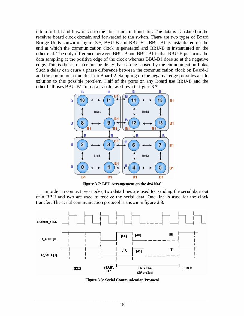
into a full flit and forwards it to the clock domain translator. The data is translated to the receiver board clock domain and forwarded to the switch. There are two types of Board Bridge Units shown in figure 3.5; BBU-B and BBU-B1. BBU-B1 is instantiated on the end at which the communication clock is generated and BBU-B is instantiated on the other end. The only difference between BBU-B and BBU-B1 is that BBU-B performs the data sampling at the positive edge of the clock whereas BBU-B1 does so at the negative edge. This is done to cater for the delay that can be caused by the communication links. Such a delay can cause a phase difference between the communication clock on Board-1 and the communication clock on Board-2. Sampling on the negative edge provides a safe solution to this possible problem. Half of the ports on any Board use BBU-B and the other half uses BBU-B1 for data transfer as shown in figure 3.7.
Figure 3.7: BBU Arrangement on the 4x4 NoC
In order to connect two nodes, two data lines are used for sending the serial data out of a BBU and two are used to receive the serial data. One line is used for the clock transfer. The serial communication protocol is shown in figure 3.8.
Figure 3.8: Serial Communication Protocol

________________________________________________________________________16
A “11” status on the data lines marks them as ‘Idle’ and a “00” is picked as the start bits. The flit is transferred out in a 2-bit serial format after sending out the start bits. Since one flit consists of 52 bits thus it takes 26 clock cycles for all the data bits to be sent out. The line is shifted back to the Idle (“11”) status after the entire flit has been transmitted.
3.4 Problems discovered during implementation The scheme described in the section 3.3 was implemented and successfully tested on a single board. However, porting the design to multiple boards resulted in a series of intermittent errors. Although the protocol performed correctly, but the sequence of data bits sent out from one board changed to different bit values intermittently when received on the other side. This caused data corruption which resulted in a flit being dropped or misrouted. The design performed perfectly well on some I/O pins while sending out data on the other I/O pins produced significant errors. Initially, the problem was suspected to be related to the physical cables being used to connect one board to the other. As a solution, different cables were used to retest the design without any change in the results. Further compilation tests pointed out varying propagation delays when the data was directed out from different I/O pins. Since the design performed a source-synchronous serial data transfer thus the clock was also being transmitted from one board to the other which further complicated the scenarios emerging with the varying propagation delays. Various constraints were placed on the design synthesis in order to improve the system performance:
• The outgoing clock signals and the data output signals were assigned ‘Fast Output Registers’. Using this utility ensures that the tool implements an output register in a cell that has a fast, direct connection to an I/O pin. If such a fast, direct connection is not available in the I/O cell hardware, this option instructs the Fitter to lock the output register in the LAB adjacent to the I/O cell it is feeding. Using this utility helps in maximizing the I/O timing performance.
• All incoming data signals (and the incoming clock signal for the remote board) were assigned ‘Fast Input Registers’. This option also performs the I/O timing performance maximization by implementing an input register that has a fast, direct connection to an I/O pin. If that is not possible, then this option instructs the Fitter to lock the input register in the LAB adjacent to the I/O cell being fed.
• Strict timing constraints were placed on the output signals in order to ensure that the tool placed maximum effort in decreasing the propagation delay. This also ensured that the design behavior stayed consistent between two different builds.
A sequence of tests was carried out with a significant improvement in the rate of successful data transfer. However, the problem was not completely resolved. Intermittent errors of sampling the same bit pattern twice or missing a bit pattern altogether still maintained, although with a much lower percentage. As a final solution, the clock rate of the inter-board communication modules was reduced to 25 MHz (from an initial value of 50 MHz). The communication tests were repeated giving successful results this time. All the FPGA boards operate at a frequency of 50 MHz (varying phases) whereas the inter-board communication is carried out at 25 MHz (varying phases). Because of the slow inter-board connection the flit insertion rate into the system is controlled at the Resource Network Interface (RNI). At maximum, one flit is inserted every 65 clock cycles by an

________________________________________________________________________17
RNI. Controlling the flit insertion rate helps in preventing the network congestion. Increasing the communication frequency to as high as possible is one of the recommended future upgrades.

________________________________________________________________________18

________________________________________________________________________19
Chapter 4
RNI and Switch The 2x2 NoC structure implemented on one FPGA board is termed as the standard Quad-Core NoC. This chapter begins by providing an overview of the standard Quad-Core NoC structure. This is followed up with a detailed description of the RNI and the switch used in the NoC platform. Routing management details are also covered in the switch section.
4.1 Standard Quad-Core NoC - Overview The NoC platform comprises of four standard Quad-Core NoC structures connected together using the inter-board connection logic described in chapter 3. It is important to note that all the four NoC structures are identical except for the absolute addresses hard-coded onto their respective nodes. The standard Quad-Core NoC has been built by upgrading the base Quad-Core NoC [6].
Figure 4.1: System Level diagram of the Standard Quad-Core NoC

________________________________________________________________________20
Figure 4.1 shows the system level diagram of the standard Quad-Core NoC. It consists of four 5-port switches. The switches are connected with each other and to the interface components. The interface components provide the required glue logic for connecting a switch to a Board Bridge Unit (BBU). The corner nodes of the NoC platform are provided with a busy signal in order to ensure that the data is not routed out to unconnected BBUs. The design also contains the RNI and the resources. The 2x2 NoC module has been added, as a Slave Avalon component, to the system using the SOPC Builder tool. The top level design diagram of the system is shown in figure 4.2.
CPU_0
Network
Onchip_mem_0
Perf_counter_0
LED_PIO_0
JTAG_UART_0
RNI
CPU_3
Onchip_mem_3
Perf_counter_3
LED_PIO_3
JTAG_UART_3
RNI
Avalon Switch Fabric Avalon Switch Fabric
Figure 4.2: Top Level Design Diagram
Figure 4.3: Snapshot of the SOPC Builder design

________________________________________________________________________21
Each CPU in the figure 4.2 refers to a Nios II processor. A 10k on-chip memory has been provided to each processor in order to store the software executable file. In addition, performance counters have been inserted for carrying out any performance related tests as per requirement. Each processor has its own set of LEDs to facilitate easy display of various status conditions. The 2x2 NoC Module has been added as an Altera Slave component and is accessible by all four processors. Figure 4.3 shows a snapshot of the SOPC Builder design.
4.2 Resource Network Interface (RNI) RNI interfaces with the resource (Nios II) by means of the Altera Avalon bus. It is connected in the system as an Avalon slave which allows the RNI to behave like a memory slave for the Nios II processor. Using the memory offsets, data packets and the control information can be read or written to the RNI. Figure 4.4 shows the memory configuration used in the system to communicate with the RNI.
Figure 4.4: RNI Memory Configuration
The sending memory (outbox) has been further divided into 2 channels of 2Kbytes each. Alternate channels are selected when data is sent out of the resource to the RNI. Similarly, the receiving memory (inbox) has been divided into 4 receiving channels of size 2Kbytes each. These channels are used to simultaneously receive packets from multiple sources. The receive channel allocation is done automatically as the flits are received by the RNI. A ‘busy_flag’ and a ‘Ch_sourceNo’ is associated with every receive channel as shown in figure 4.5.
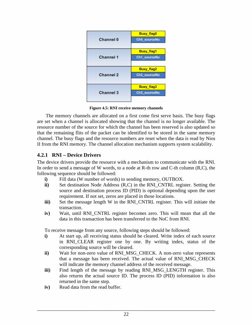
________________________________________________________________________22
Figure 4.5: RNI receive memory channels
The memory channels are allocated on a first come first serve basis. The busy flags are set when a channel is allocated showing that the channel is no longer available. The resource number of the source for which the channel has been reserved is also updated so that the remaining flits of the packet can be identified to be stored in the same memory channel. The busy flags and the resource numbers are reset when the data is read by Nios II from the RNI memory. The channel allocation mechanism supports system scalability.
4.2.1 RNI – Device Drivers The device drivers provide the resource with a mechanism to communicate with the RNI. In order to send a message of W words, to a node at R-th row and C-th column (R,C), the following sequence should be followed:
i) Fill data (W number of words) to sending memory, OUTBOX. ii) Set destination Node Address (R,C) in the RNI_CNTRL register. Setting the
source and destination process ID (PID) is optional depending upon the user requirement. If not set, zeros are placed in those locations.
iii) Set the message length W in the RNI_CNTRL register. This will initiate the transaction.
iv) Wait, until RNI_CNTRL register becomes zero. This will mean that all the data in this transaction has been transferred to the NoC from RNI.
To receive message from any source, following steps should be followed:
i) At start up, all receiving status should be cleared. Write index of each source in RNI_CLEAR register one by one. By writing index, status of the corresponding source will be cleared.
ii) Wait for non-zero value of RNI_MSG_CHECK. A non-zero value represents that a message has been received. The actual value of RNI_MSG_CHECK will indicate the memory channel address of the received message.
iii) Find length of the message by reading RNI_MSG_LENGTH register. This also returns the actual source ID. The process ID (PID) information is also returned in the same step.
iv) Read data from the read buffer.

________________________________________________________________________23
v) Clear corresponding receive flag by writing source number to RNI_CLEAR register.
In order to facilitate application development, a hardware abstraction layer (HAL) has been placed over these device drivers. Details of the HAL structure are presented in chapter 5.
4.2.2 RNI - Switch Communication The data port connecting RNI to the switch is 52 bits wide and is bidirectional. In addition there are two control signals; read_RNI and write_RNI. Both the control signals are activated/ deactivated by the switch. A switch receives and transmits data flits every fourth cycle. Write_RNI is inserted when the switch routes a data flit to the RNI. When a data flit is to be routed from the RNI to the switch, RNI places the data flit on the data port and waits for the read_RNI to be inserted. The switch inserts read_RNI only if can route the RNI inserted flit into the network. This mechanism helps in preventing network saturation.
4.3 Switch The switch interfaces with the RNI, other switches and the BBUs. It receives data flits from all interfaces and is responsible for making the routing decisions accordingly. The following sections explain the process in detail.
4.3.1 Routing Management NoC platform uses the dimension-order routing as the routing algorithm. Dimension-order routing scheme proposes a deterministic strategy for routing in multidimensional networks. Specific dimension order is chosen and the packet flits are routed along the paths in that order. The mesh network operates on the Y-X routing order. When a flit reaches a switch, the switch compares the destination node address with its local node address. Based on the result of the comparison, if the flit is required to be routed in both X and Y dimensions, it is first routed along the Y-dimension path. Once the switch is in the desired Y-dimension (desired row), the routing required along the X-dimension path is carried out. The absolute address of the destination node is specified by the resource (Nios II processor) to the resource network interface (RNI). The packet (comprising of multiple flits) is generated inside the RNI in response to the command received from the resource. The switch uses the destination ID in the flit header field to make routing decisions. The ‘Hop Count’ field is incremented by the switch every time the flit moves from one node to the other (termed as a Hop) and is utilized when making a routing decision.
Figure 4.6: Flit Format

________________________________________________________________________24
Since the board to board communication component (BBU) operates serially, thus priority is given to the flits coming in from the ports connected to the BBU. This ensures that these flits are not routed back to their source node because of network congestion as that could prove to be quite expensive in terms of time. In addition, before routing flits to the ports connected to the BBU, it is ensured that the Board-Bridge Unit is ready to accept data (keeping in view the fact that the BBU operates slower than the rest of the network because of its serial nature). Corner switches (which are not connected to any off-board switches) are provided with a permanent BBU-busy signal. This prohibits the switch from routing data in that direction. The NoC platform uses ‘Bufferless Flow Control’. This means that the switches are not equipped with any buffers. Thus, incoming flits are not stored and must be routed out at the same rate at which they arrive.
4.3.2 Switch Interfaces The switch is interfaced with three different types of entities:
• Another Switch • RNI • Board-Bridge Unit
The port connecting two switches is 52 bits wide and is bidirectional. A switch receives and transmits data flits every fourth cycle. The same protocol is used for communication with RNI, the exception being the read/write signals which are activated/ deactivated by the switch as per requirement. The switch interface to the Board-Bridge Unit (BBU) is shown in figure 4.7. In order to keep the switch design as generic as possible, interface logic unit has been added between the switch and the BBU.
Figure 4.7: Switch - Board-Bridge Unit Interface
The switch-ILU interface follows the same protocol as is used in the switch-to-switch communication. The only additional signal that comes into the switch connected to a BBU is that of ‘fifo_full’, which is used to check the output port availability while making a routing decision. The details of the signals used by the communication protocol between the ILU and the BBU are described in Table 4.1. The BBU – ILU communication protocol is shown in figure 4.8.

________________________________________________________________________25
Transmission from the ILU to the BBU is carried out in the following steps: i) When the BBU is ready to receive data from the ILU, it turns FIFO_FULL to 0 ii) When the ILU has the data ready to be sent to the BBU, and FIFO_FULL is 0,
it turns WR_FIFO to 1 and puts the data on the FIFO_IN iii) BBU detects the WR_FIFO signal on the next clock cycle and picks the data
from FIFO_IN iv) BBU turns the FIFO_FULL signal high v) ILU turns the WR_FIFO signal low once the data is sent
Signal Name Width Description FIFO_FULL 1’ Turned to ‘0’ by BBU when it is ready to receive data from the
Interface logic. Resets to ‘0’ when data is received i.e. when WR_FIFO is detected as high
WR_FIFO 1’ Turned to ‘1’ by Interface logic when FIFO_FULL is detected to be high and the Interface logic has some data to send to BBU. Reset to ‘0’ after data is sent
FIFO_IN 52’ Data bus: From Interface logic to BBU DATA_RDY 1 Turned to ‘1’ by the BBU when it is ready to send data to Interface
logic. Resets to ‘0’ when data is picked by the Interface logic i.e. when RD_FIFO is detected as high
FIFO_OUT 52’ Data bus: From BBU to Interface logic RD_ FIFO 1’ Turned to ‘1’ in the cycle in which data is picked from BBU. Resets
to ‘0’ otherwise
Table 4.1 Signal Description
Figure 4.8: BBU-ILU communication protocol

________________________________________________________________________26
The BBU to ILU transmission is described in the following steps: i) When the BBU has a data flit to be sent out to the ILU, it turns DATA_RDY
to 1 and puts data flit on the bus FIFO_OUT ii) The ILU detects the DATA_RDY being high on the next clock cycle and
picks the data flit from FIFO_OUT iii) ILU makes the signal RD_FIFO turn to 1 the same cycle it picks the data iv) BBU detects the RD_FIFO being high on the next cycle, and turns
DATA_RDY to 0 v) ILU turns RD_FIFO to 0 after the data has been picked
4.3.3 Switch Architecture The switch internal architecture is shown in figure 4.9. One routing decision cycle of the switch requires 4 clock cycles to complete its operation. One routing decision cycle consists of taking input from all 5 sources, evaluating the routing requirements, generating the required switch matrix to connect the inputs to the most appropriate outputs and then finally sending the data flits out.
Figure 4.9: Switch Architecture

________________________________________________________________________27
The switch operates in 4 control cycles: 0, 1, 2, and 3. The receiver components receive the data flits from the input source and generate the signals required by the arbitration logic in control cycle 3. In control cycle 0, routing requirements of all the input sources are evaluated and these are utilized to generate the next configuration of the switch connection matrix in control cycle 1. Once the connections are updated, the read/write signals of the RNI are generated in control cycle 2. The transmitter units transmit the data in control cycle 3. Arbitration Logic (AL) The arbitration mechanism is employed to determine how to allocate the output channels to the incoming data flits. The internal architecture of the arbitration logic unit is shown in figure 4.10.
Figure 4.10: Arbitration Logic - Internal Architecture
As a first step, preferred direction matrices are generated for all 5 input sources. These matrices contain the information about the desired output port of every input source and also the preferred alternate port if the actual required port is not available. Since the ports connected to the BBU are the slowest because of their serial nature, thus they are considered a bottleneck for the NoC platform with respect to communication. It is ensured during output channel allocation that a flit coming in from one of the BBU connected ports is given priority and is not misrouted back to its originator or onto another BBU connected port. Also prior to making a routing decision

________________________________________________________________________28
regarding the BBU connected output ports, it is ensured that the Board-Bridge Unit is not busy. The arbitration process is completed by the generation of the next switch matrix configuration, which is done while keeping in view the priority of the input ports and the availability of the desired output ports.

________________________________________________________________________29
Chapter 5
Hardware Abstraction Layer Hardware abstraction layer (HAL) is a runtime environment that provides a simple device driver interface for programs to communicate with the underlying hardware. This chapter presents the HAL designed for communication with RNI in the NoC platform. Thorough details of the supported MPI routines are presented in this chapter.
5.1 Message Passing Interface (MPI) HAL device driver abstraction provides a clear distinction between the device driver software and the application. The driver abstraction promotes reusable application code that is resistant to changes in the underlying hardware. The NoC platform is based on a packet based communication paradigm where a message consisting of one or more packets is sent over the network from one node to the other. Thus the naturally inclined HAL design would be that of a message passing library consisting of a collection of message passing routines. These routines could be embedded in the application code to accomplish send, receive and other message passing operations.
Figure 5.1: System HAL - Top view
Message Passing Interface (MPI) is a specification for message passing libraries, designed to be a standard for distributed memory, message passing and parallel

________________________________________________________________________30
computing systems. MPI is the only message passing library that can be considered a standard [9]. Designing a HAL based on MPI, in addition to standardization, also brings portability i.e. source code modification would be down to a minimum when porting application from a different platform which supports MPI. MPI Communication Routines MPI has more than 115 routines, although less than half of them are actually used to perform communication operations. Those that are, can be divided into two major categories: Point-to-Point communication and collective communication routines [9]. Point-to-Point communication routines provide the data exchange services between a programmer specified send task and a programmer specified receive task. A variety of routines fall under this category which can be divided into four groups:
• Blocking • Non-Blocking • Persistent Communication • Completion/ Testing
Collective communication routines, on the other hand, facilitate the involvement of all tasks within the communicator in a certain communication operation. Almost all the routines in this category are blocking, exception being some recent MPI implementations which utilize non-blocking corollaries specified by MPI-2. The former category is the one which is used in the NoC platform. MPI Message Passing Protocols An MPI message passing protocol describes the policies and methods used internally by an MPI implementation in order to accomplish successful message delivery. These are not defined in the MPI standard but instead have been left for the implementors to design. Therefore, these generally vary from one implementation to the other because of several factors e.g. the underlying hardware [9]. Two of the most commonly employed MPI protocols are:
i) Eager Eager is an asynchronous communication protocol i.e. a send operation is permitted to complete without acknowledgement from a matching receive.
ii) Rendezvous Rendezvous is a synchronous MPI protocol i.e. it requires acknowledgement from a matching receive in order for the send operation to complete.
Eager protocol performs better than Rendezvous with respect to timing but the actual magnitude of the improvement is implementation dependent. Figure 5.2 shows a comparison between Eager and Rendezvous using IBM’s MPI. An MPI implementation may also use different protocols as a combination within the same MPI routine. For example, an implementation may switch between the two above described protocols depending upon the size of the message.

________________________________________________________________________31
Figure 5.2: Eager vs Rendezvous Protocol
5.2 Supported MPI-Routines The NoC platform supports five standard MPI-based routines which form the message passing library used as the HAL. The library can further be enhanced by adding additional routines when the requirement arises. MPI Initialization Routine This routine is called only once at the start of the execution in order to initialize the MPI system. Figure 5.3 provides the relevant details.
Figure 5.3: MPI Initialization Routine
MPI Standard Send and Receive Routines The standard send and receive are available for simple send/receive operations. Details are provided in figures 5.4 and 5.5. MPI PID (Process ID) – based Send and Receive Routines The standard send and receive routines are sufficient to fulfill the communication requirements if there is only one active process per node in the network. However, the

________________________________________________________________________32
NoC platform also supports systems having multiple processes on a single node. In that case, the process ID (PID) based send and receive routines are used. The details of the PID-based MPI Send/Receive routines are provided in figures 5.6 and 5.7.
Figure 5.4: MPI Standard Send Routine
Figure 5.5: MPI Standard Receive Routine
The standard send function can only be matched with a standard receive routine. The PID-based send function, however, can be mixed and matched with any of the two receive routines. The PID-based Send Routine also takes the source and destination PID as arguments in addition to the arguments of the Standard Send Routine. The PID-based Receive Routine is non-blocking i.e. a certain application process can call the routine in order to check if any message has been received for it from a pre-specified process of a pre-specified node. The routine returns a ‘1’ or ‘0’ marking the presence or absence of the desired message.

________________________________________________________________________33
Figure 5.6: MPI PID-based Send Routine
Figure 5.7: MPI PID-based Receive Routine
5.3 Message Transfer Protocol This section describes the generic routine operation at a lower abstraction level. When a message is to be transmitted, the user application fills the application buffer with the message. Then a pointer to this application buffer is passed to the MPI routine along with other required parameters e.g. message length, destination ID etc. The MPI routine utilizes the device drivers to copy the data from the application buffer to the system buffer. RNI is equipped with an ‘output system buffer’ of size 1024 bytes. Since the

________________________________________________________________________34
payload of one flit is 32 bits thus the RNI output system buffer is capable of holding the payload of 256 flits at a time. This buffer has been divided into two channels which are alternately selected by the MPI routine to send out data. Once the data has been copied into the system buffer, the routine copies the control parameters into the Command Register of RNI.
Figure 5.8: Message transfer from resource 1 to resource 2
The Command Register is shown in figure 5.9. The routine copies required system buffer channel ID, message length, destination node ID and the source/destination PID into the command register. Writing to the register initiates the data transfer.
Figure 5.9: Command Register
Figure 5.10: Setup Flit
Figure 5.11: RNI Control Register
RNI formulates the packets as per the directives passed to the Command Register and sends them out to the network. Every outgoing packet has two additional flits at the beginning: a setup flit followed by a flit carrying the global time stamp. The remaining flits are all data flits. Since the output system buffer can hold only 128 flits, thus a maximum of 126 data flits can be sent out in any packet. The setup flit format is shown in the figure 5.10. The global time stamp is the 40 bit value of a slow tick clock (0.5 MHz) inside RNI. Its most significant 8 bits are sent out in the setup flit and the remaining 32
________________________________________________________________________35
are sent out in the next flit. The time stamp is reserved for the future usage as s debugging facilitation feature. The receiving RNI stores the packets in its input system buffer. Each RNI is equipped with a system buffer of 2048 bytes. This buffer is further divided into four channels of 512 bytes each. Since the payload per flit is 32 bits, thus one channel is capable of storing 128 flits. Both blocking and non-blocking MPI receive routines have been designed. Thus the user application can either wait for the data reception or just scan through the RNI interrupt register to see if any packets have been received. In case of data reception, the interrupt register points to the channel of the input system buffer in which the data has been stored. Data can be received from four different resources at any point of time and the interrupt register provides the IDs of all four channels in that case. Each channel has an associated RNI control register. The generic format is shown in figure 5.11. Thus by only reading the control register of a certain channel, it is possible to find out the source of the data, the ID of the sending process and the ID of the process for which the data has been sent. This information is sufficient for the Process ID based receive routine to decide whether the desired data has been received or not. The standard send routine sends the source and destination PIDs as zeros and the receive routine does not decode the received source and destination PIDs. The device drivers provide enough flexibility for the MPI library to be extended by further message passing routines.

________________________________________________________________________36

________________________________________________________________________37
Chapter 6
Demonstration and Evaluation This chapter describes the demonstration and evaluation details of the NoC platform. Details of two applications; the ‘Game of Life’ and the ‘Lamp-Light method’ have been provided. The chapter also gives out the performance figures extracted from the NoC platform and ends by giving out the final system specifications.
6.1 Game of Life (GoL) In order to demonstrate the functionality of the NoC platform, an application capable of exercising and verifying the different features of the platform is necessary. The best verification display for the user could be in the form of some sort of pattern generation on the LEDs based on the successful inter-communication of various nodes. Conway’s Game of Life is used for this purpose.
6.1.1 Background Game of Life (GoL), proposed by British Mathematician John Horton Conway in 1970, is a set of rules that govern the behavior of a 2-dimensional cell pattern. The pattern develops stepwise with the initial starting pattern being considered as a ‘seed’ for the system. In the 2-D grid of square cells, each cell has one of the two possible states, live or dead. Every cell interacts with its eight neighbors, which are the cells that are directly adjacent to it horizontally, vertically or diagonally. Rules of the Game of Life Based on the status of the neighboring cells, each cell jumps to a next state with respect to a specific set of rules [10]:
i) A living cell survives only if it has 2 or 3 living cells otherwise it dies ii) A cell comes to life (birth process) only if it has exactly three live neighbors
These two rules have an amazing ability to generate complex and interesting new patterns depending on the seed of the system. The first generation is created by applying the above rules simultaneously to all the cells in the seed, births, deaths and survivals

________________________________________________________________________38
happen simultaneously. The discrete moment at which this happens is called a tick. The rules are applied repeated to the created generations to produce further generations. Patterns Many different types of patterns exist and can be utilized as the seed of the system. They can broadly be divided into three classes:
i) Still Life: Static patterns which do not change their position or state e.g. block, bi-block, hives, leaves etc.
ii) Spaceships: The patterns that translate themselves across the board e.g. glider.
Figure 6.1: Still Life and Spaceship patterns
iii) Oscillators: A superset of still life – these patterns repeat themselves with a specific period e.g. blinker (period 2), star (period 3) etc.
Figure 6.2 Oscillator Patterns
Since still life maintains its initial state throughout the pattern generation process so it is not an interesting choice. The NoC platform consists of a 4x4 grid of nodes, which is too small for using any of the spaceship patterns because such patterns translate away from the point of origin. Usage of such a pattern as a seed would mean that the system would have to be reset many times as all the cells would die within 2-3 generations. Oscillators, on the other hand, prove to be a much better choice. Figure 6.2 shows the oscillator patterns Tode and Blinker which have a period 2. These patterns constantly oscillate between the two forms shown in the figure. These oscillator patterns not only fit the 4x4 grid easily but also provide ample variation in the output without any requirement for performing a system reset. Pattern Tode is thus used as a seed for the NoC platform.
6.1.2 Implementation Since the GoL implementation requires that all the cells should be updated in the same tick thus a special synchronization scheme has been adopted in order to ensure that all the NoC nodes update their life state in sync with each other. The scheme also controls the
________________________________________________________________________39
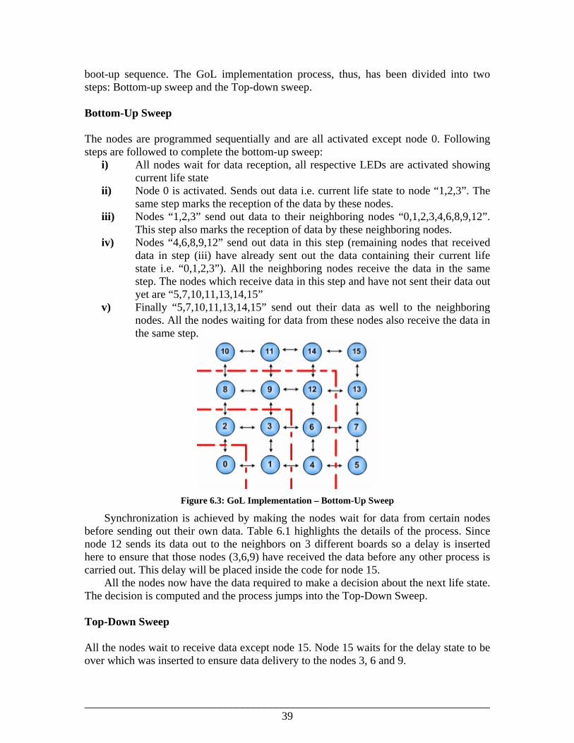
boot-up sequence. The GoL implementation process, thus, has been divided into two steps: Bottom-up sweep and the Top-down sweep. Bottom-Up Sweep The nodes are programmed sequentially and are all activated except node 0. Following steps are followed to complete the bottom-up sweep:
i) All nodes wait for data reception, all respective LEDs are activated showing current life state
ii) Node 0 is activated. Sends out data i.e. current life state to node “1,2,3”. The same step marks the reception of the data by these nodes.
iii) Nodes “1,2,3” send out data to their neighboring nodes “0,1,2,3,4,6,8,9,12”. This step also marks the reception of data by these neighboring nodes.
iv) Nodes “4,6,8,9,12” send out data in this step (remaining nodes that received data in step (iii) have already sent out the data containing their current life state i.e. “0,1,2,3”). All the neighboring nodes receive the data in the same step. The nodes which receive data in this step and have not sent their data out yet are “5,7,10,11,13,14,15”
v) Finally “5,7,10,11,13,14,15” send out their data as well to the neighboring nodes. All the nodes waiting for data from these nodes also receive the data in the same step.
Figure 6.3: GoL Implementation – Bottom-Up Sweep
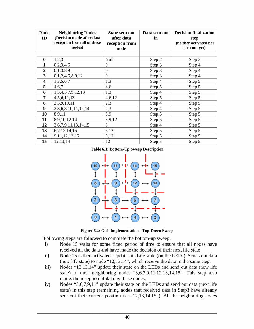
Synchronization is achieved by making the nodes wait for data from certain nodes before sending out their own data. Table 6.1 highlights the details of the process. Since node 12 sends its data out to the neighbors on 3 different boards so a delay is inserted here to ensure that those nodes (3,6,9) have received the data before any other process is carried out. This delay will be placed inside the code for node 15. All the nodes now have the data required to make a decision about the next life state. The decision is computed and the process jumps into the Top-Down Sweep. Top-Down Sweep All the nodes wait to receive data except node 15. Node 15 waits for the delay state to be over which was inserted to ensure data delivery to the nodes 3, 6 and 9.
________________________________________________________________________40
Node ID
Neighboring Nodes (Decision made after data reception from all of these
nodes)
State sent out after data
reception from node
Data sent out in
Decision finalization step
(neither activated nor sent out yet)
0 1,2,3 Null Step 2 Step 3 1 0,2,3,4,6 0 Step 3 Step 4 2 0,1,3,8,9 0 Step 3 Step 4 3 0,1,2,4,6,8,9,12 0 Step 3 Step 4 4 1,3,5,6,7 1,3 Step 4 Step 5 5 4,6,7 4,6 Step 5 Step 5 6 1,3,4,5,7,9,12,13 1,3 Step 4 Step 5 7 4,5,6,12,13 4,6,12 Step 5 Step 5 8 2,3,9,10,11 2,3 Step 4 Step 5 9 2,3,6,8,10,11,12,14 2,3 Step 4 Step 5
10 8,9,11 8,9 Step 5 Step 5 11 8,9,10,12,14 8,9,12 Step 5 Step 5 12 3,6,7,9,11,13,14,15 3 Step 4 Step 5 13 6,7,12,14,15 6,12 Step 5 Step 5 14 9,11,12,13,15 9,12 Step 5 Step 5 15 12,13,14 12 Step 5 Step 5
Table 6.1: Bottom-Up Sweep Description
Figure 6.4: GoL Implementation - Top-Down Sweep
Following steps are followed to complete the bottom-up sweep: i) Node 15 waits for some fixed period of time to ensure that all nodes have
received all the data and have made the decision of their next life state ii) Node 15 is then activated. Updates its Life state (on the LEDs). Sends out data
(new life state) to node “12,13,14”, which receive the data in the same step. iii) Nodes “12,13,14” update their state on the LEDs and send out data (new life
state) to their neighboring nodes “3,6,7,9,11,12,13,14,15”. This step also marks the reception of data by these nodes.
iv) Nodes “3,6,7,9,11” update their state on the LEDs and send out data (next life state) in this step (remaining nodes that received data in Step3 have already sent out their current position i.e. “12,13,14,15”). All the neighboring nodes

________________________________________________________________________41
also receive data in the same step. The nodes which receive data in this step and have not sent their data out yet are “0,1,2,4,5,8,10”
v) Finally node “0,1,2,4,5,8,10” update their life state on LEDs and send out their data (new life state) as well. All the nodes waiting for data from these nodes also receive the data in the same step.
Since node 3 sends its data out to the neighboring nodes on 3 different boards, so a delay is inserted here to ensure that those nodes (6,9,12) have received the data. This delay state is to be placed inside the code for node 0. All the nodes thus have the data required to make a decision about the next state. The decision is computed and all the nodes await data reception except node 0. Node 0 waits for the delay state to be over and then again a bottom-up sweep is activated. The process continues jumping between bottom-up and top-down sweep states producing the next generations on the LEDs. Table 6.2 shows the details of the top-down sweep. Node
ID Neighboring Nodes
(Decision made after data reception from all of these
nodes)
State sent out after data
reception from node
Data sent out in
Decision finalization step
(neither activated nor sent out yet)
0 1,2,3 3 Step 5 Step 5 1 0,2,3,4,6 3,6 Step 5 Step 5 2 0,1,3,8,9 3,9 Step 5 Step 5 3 0,1,2,4,6,8,9,12 12 Step 4 Step 5 4 1,3,5,6,7 3,6,7 Step 5 Step 5 5 4,6,7 6,7 Step 5 Step 5 6 1,3,4,5,7,9,12,13 12,13 Step 4 Step 5 7 4,5,6,12,13 12,13 Step 4 Step 5 8 2,3,9,10,11 3,9,11 Step 5 Step 5 9 2,3,6,8,10,11,12,14 12,14 Step 4 Step 5
10 8,9,11 9,11 Step 5 Step 5 11 8,9,10,12,14 12,14 Step 4 Step 5 12 3,6,7,9,11,13,14,15 15 Step 3 Step 4 13 6,7,12,14,15 15 Step 3 Step 4 14 9,11,12,13,15 15 Step 3 Step 4 15 12,13,14 Null Step 2 Step 3
Table 6.2: Top-Down Sweep Description
Result Demonstration The Nios development board provides eight individual LEDs; D0 to D7. These are connected to the general purpose I/O pins on the Stratix II device. The corresponding LED is turned on by driving logic 1 on the Stratix II device pin. In the NoC platform, this 8 LED pack has been divided into groups of 2 resulting in four separate modules. Each LED group has been connected to one core in the system. Core 0 is connected to [D0,D1], Core 1 with [D2,D3], Core 2 with [D4,D5] and Core 3 with [D6,D7]. These LED groups display the life status of their corresponding node during the GoL execution.

________________________________________________________________________42
Figure 6.5: The NoC platform
The implementation is in its final phase. Individual core firmware has been designed in accordance with the above given details. Currently some software bugs are being removed. It is expected that the application will be functional at the time of the project presentation.
6.1.3 Problems encountered during implementation Packet Flit Re-ordering Re-ordering the flits, received out of sequence due to misrouting, was initially one of the optional features of the NoC platform. As can be seen from the details previously provided, multiple cores send out their status data in the same step in time. This sharp increase in the network traffic causes some flits to be misrouted, especially keeping the fact in view that some channels operate at a faster speed than others. Thus there is a high probability that flits of a certain packet might reach their destination node out of the original sequence. Therefore, RNI in the NoC platform has been equipped with a flit re-ordering module. The flits received are re-arranged into their original sequence before they are forwarded to the resource. The 7-bit flit IDs are used for this purpose. RNI considers the flit IDs as an offset to the RNI receive memory buffer address. The flits are thus stored in the RNI receive memory buffer in the order in which the flit IDs have been assigned. The sequence in which the flits are received thus has no impact on the design. Console/Tool Limitation and Solution The NoC platform needs four configuration files to be downloaded onto four FPGAs for demonstration, where each FPGA hosts a standard Quad-Core NoC. All the 4 cores on an FPGA also need to be programmed with their corresponding software executables.

________________________________________________________________________43
Quartus II, the Altera design tool, is fully capable of downloading the FPGA configuration files to all the 4 FPGAs from the same host computer system. However, using the same host system to download the software executables onto the cores in all the 4 boards is not possible. The problem in this case is that each core is assigned a unique instance number at the time of its creation. The instance numbers of all cores within an FPGA system are unique, but they overlap with each other if there are multiple FPGA systems involved. The solution to this problem is either to use as many host systems as the target boards or to download the code permanently onto the FPGA. Since the system needs to be further extended in the future therefore having as many host systems as the target boards is not a feasible solution. The second option has thus been utilized in the NoC platform. Nios development board is equipped with a 16 Mbyte AMD AM29LV128M flash memory device connected to the Stratix II device that can be used for two purposes:
• A Nios II embedded processor implemented on the Stratix II device can use the flash as general-purpose readable memory and nonvolatile storage.
• The flash memory can hold Stratix II device configuration data that is used by the configuration controller to load the Stratix II device at power-up.
A Nios II processor design in the FPGA can identify the 16 Mbyte flash memory in its address space, and can program new data (either new Stratix II configuration data, Nios II embedded processor software, or both) into flash memory. The Nios II embedded processor software includes subroutines for writing and erasing flash memory. More details on programming the flash with the configuration file and the software executables can be found in Appendix-C.
6.2 Lamp-Light Method Lamp-Light method is a menu based console application designed to demonstrate successful node to node communication and to measure the system performance figures of the NoC platform. The Nios II processor (resource) of node 0 operates as the system controller node. All the other nodes are passive and wait for an input from the system controller node. The system controller node is connected to the host computer system using the Altera Debug Client.
Figure 6.6: Lamp-Light Method
All the nodes in the NoC platform are connected to a distinct set of 2 LEDs. At system startup, all the LEDs have a status 0 and are thus turned off. The menu of the system controller node takes two inputs from the user:
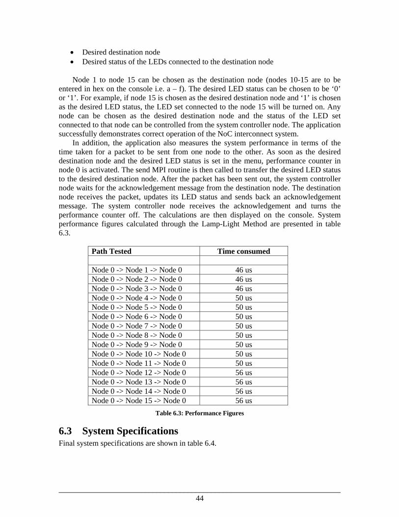
________________________________________________________________________44
• Desired destination node • Desired status of the LEDs connected to the destination node
Node 1 to node 15 can be chosen as the destination node (nodes 10-15 are to be entered in hex on the console i.e. a – f). The desired LED status can be chosen to be ‘0’ or ‘1’. For example, if node 15 is chosen as the desired destination node and ‘1’ is chosen as the desired LED status, the LED set connected to the node 15 will be turned on. Any node can be chosen as the desired destination node and the status of the LED set connected to that node can be controlled from the system controller node. The application successfully demonstrates correct operation of the NoC interconnect system. In addition, the application also measures the system performance in terms of the time taken for a packet to be sent from one node to the other. As soon as the desired destination node and the desired LED status is set in the menu, performance counter in node 0 is activated. The send MPI routine is then called to transfer the desired LED status to the desired destination node. After the packet has been sent out, the system controller node waits for the acknowledgement message from the destination node. The destination node receives the packet, updates its LED status and sends back an acknowledgement message. The system controller node receives the acknowledgement and turns the performance counter off. The calculations are then displayed on the console. System performance figures calculated through the Lamp-Light Method are presented in table 6.3.
Path Tested Time consumed Node 0 -> Node 1 -> Node 0 46 us Node 0 -> Node 2 -> Node 0 46 us Node 0 -> Node 3 -> Node 0 46 us Node 0 -> Node 4 -> Node 0 50 us Node 0 -> Node 5 -> Node 0 50 us Node 0 -> Node 6 -> Node 0 50 us Node 0 -> Node 7 -> Node 0 50 us Node 0 -> Node 8 -> Node 0 50 us Node 0 -> Node 9 -> Node 0 50 us Node 0 -> Node 10 -> Node 0 50 us Node 0 -> Node 11 -> Node 0 50 us Node 0 -> Node 12 -> Node 0 56 us Node 0 -> Node 13 -> Node 0 56 us Node 0 -> Node 14 -> Node 0 56 us Node 0 -> Node 15 -> Node 0 56 us
Table 6.3: Performance Figures
6.3 System Specifications Final system specifications are shown in table 6.4.

________________________________________________________________________45
NoC Sixe 4x4 Topology Mesh Resource Category Homogoneous
(Nios II processors) Flow Control Bufferless Clock Domain Plesiochronous
(Four synchronous Domains) System Clock Speed 50 MHz Inter-board Comm. Clock Speed 25 MHz Addressing Scheme Absolute Routing Algorithm Dimension-Order (Y before X) Flit Size 52 bits (Payload 32 bits) Maximum Data Flits/ Packet 126 Data Rate: Switch to Switch (on board)
2600 Mbit/s (50 M Flit/s)
Data Rate: Switch to Switch (inter-board)
50 Mbit/s (~1 M Flit/s)
Interconnect scheme scalable Yes RNI receive buffer size 2048 bytes RNI send buffer size 1024 bytes On-Chip memory/ core 10Kbytes HAL Design Yes (MPI based) Used FPGA device EP2S60F672C5ES Family Stratix II Logic Utilization 28 % Combinational ALUTS 18 % Dedicated Logic Registers 22 % Total Memory Block bits 31 %
Table 6.4: System Specifications

________________________________________________________________________46
________________________________________________________________________47
Chapter 7
Conclusions and Future Work The main objective of the work was to design and implement a multi-core 4x4 NoC-platform using multiple FPGA (field programmable gate array) boards. This has been achieved successfully. The NoC platform implemented is equipped with a 5-port switch capable of managing the routing requirements. Stable inter-board communication units have also been designed and implemented for successful operation of the platform. MPI based hardware abstraction layer has also been designed for facilitating development of reusable application code which is resistant to changes in the underlying hardware. Applications have been developed demonstrating the correct operation of the NoC platform and also providing the performance figures. In addition, the optional task of the designing and implementing flit re-ordering scheme has also been completed. Thus looking back at the objectives, it is clear that the targets have been met. In addition to being utilized significantly for testing and verification of various NoC methodologies, the current plesiochronous NoC platform can also serve as a solid reference for designing a customized hardware NoC platform. There is, however, a lot of interesting work that can be carried out in the future in order to further upgrade the platform. Some of the main tasks are listed below:
• Maximizing the switch-to-switch (inter-board) data rate: Further testing can be carried out for guaranteeing a stable operation of the BBUs at a clock speed higher than the currently used 25 MHz. It will be interesting to check out the system behavior at clock speed higher than the system clock speed of 50 MHz. The system currently displays a data clock race condition at 50 MHz but using a multiple of the currently used communication clock speed (e.g. 75 MHz) might produce promising results. It may also be interesting to carry out communication tests at 50MHz but with the communication clock phase being varyingly displaced from the system clock phase.
• RNI-Switch data flow protocol: RNI currently has only 4 receive memory channels. Since it is possible for the data packets to arrive simultaneously from more than 4 sources, so it is of utmost importance that a certain data flow control protocol between RNI and the switch be designed. If all the RNI receive channels are busy, then this status should be forwarded to the Switch. The protocol should be so designed that the switch is aware of the source IDs for which the channel reservation has been made. This would ensure that the remaining flits of a half received packet would still be forwarded to the RNI even if the status signal shows the RNI channels to be unavailable.

________________________________________________________________________48
• Fault tolerant design: Adding a CRC to the transmitted flits and devising a control mechanism for packet/flit retransmission in case of an error would be a good starting point for achieving a fault tolerant NoC design. This could later be upgraded by defining and implementing strategies for dealing with broken links.

________________________________________________________________________49
References [1] G.E. Moore, Crammming more components onto integrated circuits. Electronics, 38(5), 1965. [2] Moore's Law, Made real by Intel innovation, Intel Corporation, http://www.intel.com/technology/mooreslaw/ Last checked 1st May 2009. [3] L. Benini and G. De Micheli, Networks on Chip: A New SoC Paradigm, Computer, vol. 35, no. 1, Jan. 2002, pp. 70-78. [4] F. Angiolini et al., Contrasting a NoC and a Traditional Interconnect Fabric with Layout Awareness, Proc. Design, Automation and Test in Europe Conf. (DATE 06), IEEE Press, 2006, pp. 124-129. [5] Juha-Pekka Soininen, Axel Jantsch, Martti Forsell, Antti Pelkonen, Jari Kreku, and Shashi Kumar. Extending platform-based design to network on chip systems. In Proceedings of the International Conference on VLSI Design, January 2003. [6] Johnny Öberg, Roger Mellander, and Said Zahrai. The ABB NoC – a Deflective Routing 2x2 Mesh NoC targeted for Xilinx FPGAs. In the proceedings of the FPGAworld Conference, September 2008. [7] Nios Development Board, Reference Manual, Startix II Edition, Altera Corporation July 2005. [8] R. Ginosar, Fourteen Ways to Fool Your Synchronizer, Proc. 9th IEEE Int'l Symp. Asynchronous Circuits and Systems (ASYNC 03), IEEE CS Press, 2003, pp. 89–96. [9] MPI Performance Topics, SP Parallel Programming II Workshop, Maul High Performance Computing Centre (MHPCC), University of Hawaii. http://www.mhpcc.edu/training/workshop2/mpi_performance/MAIN.html#Review Last checked: 1st May 2009. [10] Gunnar Johnsson, Conway’s Game of Life, Department of Mathematics. Royal Institute of Technology, Sweden http://www.math.kth.se/~gunnarj/LIFE/WLIF/wlcframes.html Last checked: 1st May, 2009

________________________________________________________________________50

________________________________________________________________________51
Appendix A
List of Abbreviations AL Arbitration Logic ALM Adaptive Logic Module ASIC Application-Specific Integrated Circuit BBU Board-Bridge Unit FIFO First In First Out FPGA Field-Programmable Gate Array GoL Game of Life HAL Hardware Abstraction Layer HDL Hardware Description Language IDE Integrated Development Environment ILU Interface Logic Unit LED Light Emitting Diode MPI Message Passing Interface MPSoC Multi-Processor System-on-Chip MTBF Mean Time between Failure PID Process Identifier PLL Phase-Locked Loop RNI Resource Network Interface NoC Network-on-Chip NREC Non-Recurring Engineering Cost RTL Register Transfer Level SoC System-on-Chip

________________________________________________________________________52
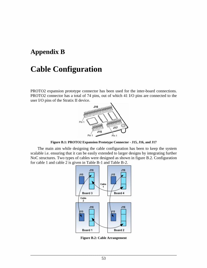
________________________________________________________________________53
Appendix B
Cable Configuration PROTO2 expansion prototype connector has been used for the inter-board connections. PROTO2 connector has a total of 74 pins, out of which 41 I/O pins are connected to the user I/O pins of the Stratix II device.
Figure B.1: PROTO2 Expansion Prototype Connector - J15, J16, and J17
The main aim while designing the cable configuration has been to keep the system scalable i.e. ensuring that it can be easily extended to larger designs by integrating further NoC structures. Two types of cables were designed as shown in figure B.2. Configuration for cable 1 and cable 2 is given in Table B-1 and Table B-2.
Figure B.2: Cable Arrangement

________________________________________________________________________54
Board 1 (Board 3)
Stratix II Pin No
J16 Pin No
Board 2 (Board 4)
Stratix II Pin No
J16 Pin No
sndr_clk_UR_LR_A C21 21 sndr_clk_UL_LL_C B22 31 Dout_UR_A(1) C18 13 Din_UL_C(1) H18 39 Dout_UR_A(0) C19 14 Din_UL_C(0) J14 37 Din_UR_A(1) A20 15 Dout_UL_C(1) B21 38 Din_UR_A(0) J17 16 Dout_UL_C(0) K17 35 Dout_LR_A(1) A21 17 Din_LL_C(1) H17 36 Dout_LR_A(0) C20 18 Din_LL_C(0) B24 33 Din_LR_A(1) A22 23 Dout_LL_C(1) A24 32 Din_LR_A(0) E18 25 Dout_LL_C(0) C22 29 GND GND 19 GND GND 40
Table B-1: Cable 1 Configuration
Board 3
(Board 4) Stratix II
Pin No J16
Pin No Board 1
(Board 2) Stratix II
Pin No J15
Pin No sndr_clk_LL_LR_B H15 3 sndr_clk_UL_UR_D B20 3 Dout_LL_B(1) J15 4 Din_UL_D(1) K18 4 Dout_LL_B(0) C16 5 Din_UL_D(0) F16 5 Din_LL_B(1) A17 6 Dout_UL_D(1) H16 6 Din_LL_B(0) C17 7 Dout_UL_D(0) D17 7 Dout_LR_B(1) A18 8 Din_UR_D(1) G16 8 Dout_LR_B(0) F17 9 Din_UR_D(0) B16 9 Din_LR_B(1) K16 10 Dout_UR_D(1) B17 10 Din_LR_B(0) G17 11 Dout_UR_D(0) B18 11 GND GND 2 GND GND 1
Table B-2: Cable 2 Configuration

________________________________________________________________________55
Appendix C
Programming the Flash Memory Altera documentation provides complete details of how to program the software executable file (elf) and the FPGA configuration file (sof) onto the system flash device. The procedure, however, is described as two separate processes, one for the elf and the other for the sof. Programming the flash in this way requires a minimal set of hardware components to be present in your SOPC builder design. In addition, if you intend to burn the elf for multiple processors into the flash, then the FPGA core at the time of flash programming should contain an equal number of multiple processors as well. Adding more components into your design for flash burning support is a time consuming and tedious process. More time is wasted in system debugging and modification if the newly added components do not start working correctly on the first attempt. Also the new core takes unnecessarily larger design space as the flash support circuitry is not needed for the normal design operation. A much easier way to do this is by combining the elf with the sof file as a single bit stream and then burning it into the flash. Such a scheme does not require any additional hardware components as the sof can be burned into the flash when the FPGA device is operating under factory settings. Moreover, the design does not even need to be recompiled to generate a new sof file every time a change in the elf is made. Since a modification in a software executable file does not require any synthesis and fitter operation, the assembler can be directly invoked by a simple command to update the sof in comparatively much lesser time. The procedure has been extracted from multiple Altera documents and Altera Support Forums. The steps are as follows:
• Open your SOPC Builder design and check the “Enable non-default initialization file” option in your on-chip memory properties. Note down the name of the hex file stated in the box “User Created Initialization File”. If you are using multiple processors, repeat the process for the on-chip memory associated with every processor.
• Generate the SOPC system and recompile the Quartus design. Empty hex files of the same name as mentioned in the field “User Created Initialization File” will now be generated in the root of your design folder.
• Generate the elf files using the Nios IDE. Use the ‘elf2hex’ command to convert these to the hex format. Values of the parameters ‘base’, ‘end address’ and ‘width’, required for the command execution can be found in the SOPC builder

________________________________________________________________________56
design. Use appropriate values of these parameters depending upon the target on-chip memory.
• Overwrite the hex files automatically generated in the root of the project design folder by these new hex files generated from the elf (If your hex has a different name, change it to the one used in the SOPC system for the user created initialization file).
• There is no requirement of recompiling the design, use the following two commands using the Nios Command Shell to update the sof file,
quartus_cdb --update_mif <your quartus project name>.qpf quartus_asm <your quartus project name>.qpf
A new sof file containing the elf contents will be generated. Burn this sof into the flash (or directly into your FPGA to test if it works). The processor elf will be loaded immediately after the sof file has been downloaded onto the FPGA. Please note that this process can only be used if the processors use the on-chip memory.
Burning a sof into flash memory Use the following two commands to burn the sof into the system flash. Value of the offset and the base address may vary depending upon the flash partitioning.
• Convert ‘.sof’ to ‘.flash’ format sof2flash --offset=0x00800000 --input=xyz.sof --output=xyz.flash
• Burn the ‘.flash’ into the flash memory nios2-flash-programmer --cable="Usb-blaster [USB-0(or 1)]"
--base=0x00000000 --program xyz.flash