Embed Size (px)
Citation preview

Design and Implementation of a
Microgrid-Capable Solar Inverter
by
Gavin M. Darcey
S.B., EECS, Massachusetts Institute of Technology (2011)
Submitted to the Department of Electrical Engineering and ComputerScience
in partial fulfillment of the requirements for the degree of
Master of Engineering in Electrical Engineeringand Computer Science
at the
MASSACHUSETTS INSTITUTE OF TECHNOLOGY
September 2013
@2013 Gavin M. Darcey All rights reserved.The author hereby grants to M.I.T. permission to reproduce and
distribute publicly paper and electronic copies of this thesis documentin whole and in part in any medium now known or hereafter created.
Author..... .r . .fD t ment of Ec *al Engineering and Computer Science
A4August 30, 2013
Certified by.j
'I)
James L. Kirtley, Jr.Professor of Electrical Engineering
Thesis Supervisor
A ccepted by ............ V .......... . ...............................Prof. Albert R. Meyer
Chairman, Master of Engineering Thesis Committee

Design and Implementation of a Microgrid-Capable Solar
Inverter
by
Gavin M. Darcey
Submitted to the Department of Electrical Engineering and Computer Scienceon August 30, 2013, in partial fulfillment of the
requirements for the degree ofMaster of Engineering in Electrical Engineering
and Computer Science
Abstract
The notion of a practical microgrid - a small, interconnected system of generators andloads that operates both synchronously with a larger, centralized grid and isolatedfrom the grid, autonomously - has grown popular as electric utilities are installedmore frequently in areas lacking a pre-existing central grid. To research the effects ofboth intentional disconnects and unintentional faults within a microgrid and betweenit and the central utility, we have constructed such a system in simulation by usinghardware to simulate the real-world generators and loads of the microgrid and haveconnected it to the MIT utility.[1] The microgrid requires a clean, efficient switchingsystem in order to connect and disconnect its components, and this thesis beginswith an explanation of the control hardware and software interface implemented todo so. Next, this thesis details the design of one of the main generating sources for themicrogrid, the inverter for a hardware-simulated solar panel. Solar panels with DCoutput are virtually always connected through a power inverter to produce the usablethree-phase AC on the power grid. This particular inverter design is intended tobe control-scheme agnostic; the actual operation of it will vary with different controlalgorithms. It is designed to be a general purpose, three phase 2.3 kW power inverter,albeit with specifically added modules to suit this particular microgrid. This thesiscovers both the design of the circuit and the finished layout of its printed circuitboard.
Thesis Supervisor: James L. Kirtley, Jr.Title: Professor of Electrical Engineering
2

Acknowledgments
I would like to thank Professor Kirtley for first giving me the opportunity to work
on this project; his immense support bringing me on to the project and guidance
throughout has been invaluable. I would also like to thank Jorge Elizondo Martinez,
who was always ready to help answer any questions involving the inverter design,
and finally Jared Monnin, Michael Zieve, and Zhiyong Wang for their enormous help
during the beginning construction of the physical microgrid.
3

Contents
1 Microgrid Overview 8
1.1 Microgrid Layout .............................. 8
1.1.1 Loads ....... ............................... 9
1.1.2 Interconnection .. . . . . . . . . . . . . . . . . . . . . . . . . 10
1.2 Control Interface ....... ............................. 11
1.2.1 Control Software . . . . . . . . . . . . . . . . . . . . . . . . . 12
1.2.2 Control Hardware . . . . . . . . . . . . . . . . . . . . . . . . . 13
2 Inverter Design 15
2.1 High-power Stage . . . . . . . . . . . . . . . . . . . . . . . . . . . . . 16
2.1.1 Three-phase Bridge . . . . . . . . . . . . . . . . . . . . . . . . 16
2.1.2 O utput Filter . . . . . . . . . . . . . . . . . . . . . . . . . . . 18
2.2 G ate D river . . . . . . . . . . . . . . . . . . . . . . . . . . . . . . . . 19
2.2.1 IR 21362S . . . . . . . . . . . . . . . . . . . . . . . . . . . . . 19
2.3 Control Power and Signal Isolation . . . . . . . . . . . . . . . . . . . 20
2.3.1 Optocouplers . . . . . . . . . . . . . . . . . . . . . . . . . . . 20
2.3.2 D igital Isolators . . . . . . . . . . . . . . . . . . . . . . . . . . 21
2.3.3 G rounding . . . . . . . . . . . . . . . . . . . . . . . . . . . . . 22
2.4 Signal Measurement . . . . . . . . . . . . . . . . . . . . . . . . . . . 23
2.4.1 V oltage . . . . . . . . . . . . . . . . . . . . . . . . . . . . . . 23
2.4.2 C urrent . . . . . . . . . . . . . . . . . . . . . . . . . . . . . . 24
2.5 Signal Processing . . . . . . . . . . . . . . . . . . . . . . . . . . . . . 25
4

3 Final Layout 27
3.1 Physical Footprint ....... ............................ 27
3.2 C onclusion . . . . . . . . . . . . . . . . . . . . . . . . . . . . . . . . . 30
5

List of Figures
Microgrid block diagram. . . . . .
Microgrid loads. . . . . . . . . . .
Three-phase relay schematic. . . .
LabVIEW backend code. . . . . .
Switching control user interface. .
Interface hardware. . . . . . . . .
SSR amplifier circuit. . . . . . . .
Three-phase bridge topology. . . .
Output filters. . . . . . . . . . . .
Typical application of gate driver.
Optocoupler circuit . . . . . . . .
Digital isolator circuit. . . . . . .
Voltage sensor circuit. . . . . . .
Current sensor circuit. . . . . . .
Signal processing circuit. . . . . .
3-1 Overall view of circuit footprint.
3-2 Ground planes. . . . . . . . . .
6
1-1
1-2
1-3
1-4
1-5
1-6
1-7
2-1
2-2
2-3
2-4
2-5
2-6
2-7
2-8
9
. . . . . 10
. . . . 11
. . . . . 12
. . . . . 13
. . . . . 13
. . . . . 14
. . . . . . . . . . . . . . . . . . . 1 7
. . . . . . . . . . . . . . . . . . . 1 8
. . . . . . . . . . . . . . . . . . . 2 0
. . . . . . . . . . . . . . . . . . . 2 1
. . . . . . . . . . . . . . . . . . . 2 2
. . . . . . . . . . . . . . . . . . . 2 4
. . . . . . . . . . . . . . . . . . . 2 4
. . . . . . . . . . . . . . . . . . . 2 6
27
29

List of Tables
2.1 List of grounds used and circuit modules relative to them. . . . . . . 23
7

Chapter 1
Microgrid Overview
This chapter covers the overall microgrid construction, beginning with its physical
layout in the LEES lab space, and finishing with the interconnection and switching
system implemented as part of this thesis.
1.1 Microgrid Layout
The microgrid used in this project is a set of three hardware-simulated generators and
six basic loads, intended to model a typical commercial load that would be connected
to the grid. The current functioning generators are a linked electric motor set that
represents a diesel-powered synchronous generator and a DC power supply linked to
a power inverter, the design of which is detailed later in this thesis. The grid includes
capabilities to add a third generator in the future, which will model a wind turbine
generator system. Figure 1-1 on the next page provides an overall general schematic
of the microgrid layout. The six loads are described in the next section.
8

Diesel Engine Emulator Exciter
DO Motor Synchronous Generator
DC Supply Inwrter i Switched Passive Loads
Aind Turbine Emulotor DFIG Phase Controlled Load
DO Motor
Microgrid Breaker Load Controller
induction Motor Load
Lob (Utility) Supply Microgrid Control Microgrid Bus
Figure 1-1: System-level block diagram of complete microgrid. Note that all inter-connection lines are three-phase AC. [3]
1.1.1 Loads
The loads themselves are all balanced, three phase sets representing different types
of typical system loads. Included are two purely resistive loads, each made of three
power resistors in a wye formation, tuned to 70Q. There is a purely capacitive load
constructed from six large AC 8 0pF capacitors and a purely inductive load made from
three laminated iron cores with two air gaps and about 270 windings, for an induc-
tance of about 108mH on each phase. These loads are also in a wye formation, and
provide a total capacitive load of about 650VAR and an inductive load of 1.05kVAR,
respectively.
Beyond these four basic RLC loads, the grid also contains two more complex loads,
to model more realistic applications. The first consists of a phase-controlled load
built from three single-phase light dimmers, mounted back-to-back with the levers
mechanically coupled to control all phases simultaneously. Each dimmer is connected
in series with a 60W incandescent light bulb, and the three dimmer/bulb pairs are
again connected in a wye formation with the neutral point tied to the microgrid
neutral line.
9

These dimmers, along with the first four loads, are shown in Figure 1-2 as they
stand mounted on the microgrid.
Figure 1-2: Photograph of loads physically mounted on microgrid. Clockwise frombottom left: inductors, phase-controlled light bulbs, capacitors, two resistor banks.Induction motor not pictured.
The final load is a 1HP squirrel cage induction motor mechanically tied to a 1.5HP
DC motor. The induction motor is tied to the microgrid bus, while its linked DC
motor exists to adjust the torque loading on the induction motor.
1.1.2 Interconnection
The connections between the loads and generators, as well as the complete microgrid
and the MIT electric utility, are all handled through solid-state relays, specifically the
Carlo Gavazzi RZ3A60A55. The relays link between each isolated microgrid subsys-
tem and a central screw-terminal wire bus. These particular relays were chosen not
only for their suitably high operational voltage tolerance and inherent three-phase
connection layout, but also for their quick switching response time. Originally, only
the generators and main grid connection were routed through solid-state relays; all
load connections were handled through electromechanical relays which use solenoids
to initiate contact. However, it was determined through testing that these electrome-
10

chanical relays included a switching delay when switched after being in a prolonged
state of either on or off. For the sake of rapid disconnection at any time if necessary,
all relays were switched to the solid-state models. Figure 1-3 shows a schematic of
the solid-state relays that link each component to the main bus.
3-PHASE SSR
AIN AOUT
B IN BOUT
o C IN C_OUT6
+28V SWITCH
Figure 1-3: When the switch is moved to po-sition 2, a +28V potential difference will sit
_JLO across the control pins and all three phases willconduct. This switch models the control hard-
SWITCH ware discussed in Section 1.2.2.
1.2 Control Interface
The control of these relays has been implemented using the National Instruments
LabVIEW design platform. It was determined early in the project that the project
would need signal monitoring and measurement capability added to several places
throughout the microgrid, which was to be done using several National Instruments
data acquisition devices (DAQs). This has since been successfully built but remains
outside the scope of this document. However, the software and hardware that com-
prise the control system, which also relies on the DAQs, are detailed in this section.
11

1.2.1 Control Software
DAQmx Physical ChannelS RelayControl/port0/ine0%7 Relaycontrol/pnrtl/ - Relay -control C
CUlCK HERE TO STOP Numeric Main_GridRelay[M
D TR~y 8 uld Array
F Kcil n Scilar Retay[CW L Tab Control Resistor _RRelayM
Sampes per sec .*.. Pase Contol Rea ayCa amp
o.oof Samrslp~alesh o Is MotoRelay[
Ma n gnd 0. Determine the channelsto read
Numberofpoints IFigure 1-4: Code snippet from
LabVIEW backend control code,GeP- t used for connecting and discon-
Number of points 2 necting relays.
LabVIEW is essentially a graphical programming language, which allows the pro-
grammer to write code using flow diagrams that are then continuously executed when
run. When running, the user is presented with a front-end control panel that allows
for interaction with the code running in the background. The front control panel
for the microgrid, when executed, waits for the user to click on-screen pushbuttons,
the state of which is stored in a binary array. This array is 11 characters long, with
one bit reserved for each of the three generators, six loads, and one MIT utility con-
nection. The eleventh bit is used to initiate a short circuit by way of controlling a
separate solid-state relay which shorts the three phases of the utility line. It is in-
tended to model an accidental fault across the microgrid for future islanding (main
utility disconnection) experiments. As each button is pressed, an on-screen LED will
light up to indicate the relay is currently conducting, matching the the physical re-
lay indicator as well. Figure 1-4 is a screen capture of the main component of the
backend LabVIEW code and illustrates the sequence that is run by the control panel,
while Figure 1-5 on the following page presents the user interface for switch control.
The current microgrid interface includes significantly more capabilities beyond the
basic switch control, such as data measurement and plotting, but that work was done
outside of this thesis.
12

Figure 1-5: User-facing control panel when LabVIEW code is run. When the greenbuttons are pressed, the relays are activated and the on-screen LED lights up.
In addition to the separate pushbuttons for each relay, additional controls have
been created to initiate all connections or disconnections simultaneously. This was
implemented both for convenience when testing the grid and for safety; in the event
of an actual, unintended fault all loads and generators can be disconnected quickly
right from the control panel. These can be seen in Figure 5 as well.
1.2.2 Control Hardware
Figure 1-6: Left: DAQ for relay control. Right: arrayof BJT amplifier circuits to read DAQ input and switchrelays.
13
P. Edd 100h Almftw HeIPI IF&Tail " W i

Figure 1-6 on the previous page shows the two pieces of relay control hardware.
The LabVIEW code runs on a National Instruments USB-6008, a low-cost USB-
powered multifunction DAQ with 12 digital input/output (I/O) pins. Eleven of these
pins are tied to the software's eleven-bit binary array, and appropriately output a
transistor-transistor logic (TTL) level of OV or +5V as on-screen buttons are pressed.
Each I/O pin output is then sent to its own common-emitter amplifier (CE) circuit,
a schematic of which is seen below in Figure 1-7:
+28V
SSRIN_1
SSRIN_2
2.7k
DAQ-CHANNEL 2 NPN Figure 1-7: Schematic for pull-up CEamplifier to quickly switch solid-staterelays according to DAQ output.
This pull-up circuit is necessary because the relays require a minimum of +24VDC
at their connection terminal, which is above the capable TTL output range of the
DAQ. Additionally, the relays must be turned on quickly, which requires more current
than can be sourced by the DAQ alone. The arrangement of common-emitter ampli-
fiers, with their power rails tied to an external wall power supply tuned to +28V, is
able to activate and deactivate the relays with appropriate speed. It should be noted
that in order to control the amplifier circuit reliably, the ground pin of the DAQ must
also be tied to the ground line of the external +28V power supply.
14

Chapter 2
Inverter Design
A common power source in existing microgrids is a photovoltaic (PV) array, which
must have its DC output sent through a power inverter in order to generate the
appropriate AC waveforms to handle commercial appliances. For this microgrid,
commercially available inverters were purchased - three Enphase D380 microinverters.
These three single-phase inverters were tied together and connected to the grid just
as intended. However, it was soon discovered that these were inadequate for this
specific project due to standard industry regulations.
Underwriter Laboratories (UL) 1741 - Inverters, Converters, Controllers and In-
terconnection System Equipment for Use With Distributed Energy Resources - and
IEEE 1547 - Standard for Interconnecting Distributed Resources with Electric Power
Systems both dictate the acceptable behavior of a solar inverter while in use [6] , and
as per IEEE Std 1547.2-2008 8.1.5:"The DR [distributed resource] shall not energize
the Area EPS [electric power system] when the Area EPS is de-energized." [2] This
requirement is intended to ensure the safety of any utility personnel working in a
nominally deactivated area; all distributed resources such as solar panels are required
to shut off completely if the rest of the grid is disconnected. In other words, with no
detected outside grid voltage, commercial inverters cannot source their own voltage.
15

While perfectly reasonable for a commercial product designed for constant utility
connection, this requirement renders the Enphase inverters unusable for the microgrid
islanding experiments. It was deemed necessary to design a custom three-phase in-
verter capable of sustaining voltage output regardless of grid connection. This chapter
details the microgrid inverter design completed as part of this thesis.
2.1 High-power Stage
The main function of the inverter is to convert a large DC voltage - modeling a
photovoltaic array - into the standard three-phase AC distribution of three separate
60Hz sine waves, each 120 degrees out of phase. This requires both rapid switching
of three sets of transistor pairs and filtering on the output to eliminate unwanted
harmonics.
2.1.1 Three-phase Bridge
The inverter relies on the canonical three-phase bridge topology common to most
three-phase inverters. It consists of three sets of high/low pairs of MOSFETs (with
each pair commonly called a "totem"), where the top MOSFET of each totem is tied
to the high level of the modeled PV array. The inverter has been designed to operate
with a DC input of as high as +230V. The low MOSFET is then tied to the ground of
this high voltage, referred to in this design as COM. The three-phase bridge is shown
in Figure 2-1 on the next page.
16

MOSFET3
D3CO - ___ ______
MOSFET-2 1Z 0c
U
U
f U . . IMOSFE4
a -
D
VDD
Figure 2-1: Common three-phase bridge topology consisting of three pairs of highand low MOSFETs, each with their midpoints being sent out to filter.
Each MOSFET also includes a snubber circuit designed to limit stresses on the
semiconductor switches. Although the MOSFETs are all rated to withstand a +600V
potential across their drain and source, the stresses while switching coming from
parasitic inductances may place unanticipated strain on them. The snubber circuit is
a practical turn-off snubber [4] consisting of a single diode in parallel with a resistor,
the combination of which is in series with a capacitor. The capacitor presents a
third path for current to flow when the MOSFET is turned off, while the resistor is
included to limit the capacitor's discharge current when the switch is turned back on.
Although optimized efficiency was not the goal of the inverter, the diode is provided
to allow the capacitor charging current to avoid the resistor when the switch is turned
off.
17
MOSFEJ MOSFE 5 nJ -~ r
0' z U) ---
MOSFET 6 T
U

2.1.2 Output Filter
The output of each phase from the three-phase bridge is sent through a filter before
being delivered as the final output. The filter designed for this inverter consists of
two inductors and a capacitor on each phase, as seen in Figure 8.
VMID1 UT1
E
- FILTER2
VMID2 UT2
E
--VFILTER3
Figure 2-2: Schematic illustrating two of the three output filters, where VMID1 andVMID2 come directly from the totem midpoints in Figure 2-1. Also note that thefilters all connect line-to-line.
The filter components are currently not yet sized; the physical board layout al-
lows for a general iron core to be fitted with as many windings as necessary for the
inductors, and an extremely common capacitor footprint is used to allow for a wide
range of capacitor values to be used. This is due to the fact that a control scheme has
not yet been finalized; the filter specifications will depend on the switching algorithm
used on the MOSFETs.
Also included is a damper circuit to avoid resonance peaks while operating. This
damper circuit is a simple series RC that sits in parallel with the main filter capacitor.
Finally, it should be explicitly noted that the three phases of the inverter output are
all defined as line to line, rather than line to neutral or line to ground.
18

2.2 Gate Driver
The MOSFETs in the totem bridge are intended to be controlled through either a
microcontroller or digital signal processor (DSP), but these devices are not capable
of sourcing and sinking the current necessary to quickly charge and discharge the
MOSFET gates. Hence, a gate driver circuit must be used to effectively and rapidly
switch the MOSFETs.
2.2.1 IR21362S
To drive the MOSFET gates, it was deemed practical to use a monolithic three-
phase gate driver IC, which provides a single chip to interface with all six MOSFETs
and requires minimal outside circuitry. This inverter uses an International Rectifier
IR21362S chip, which includes built-in shoot-through delay to ensure that any par-
ticular high/low pair never has both its switches on. Doing so would short the high
input voltage (VDD) to COM, potentially causing damage both to the modeled PV
array and the inverter. Of the IR2136 family of ICs, the IR21362S was chosen due to
its active-low low side inputs. This allows for the normal 6-input control scheme, as
well as 3 inputs fed directly to the driver with the driver's high/low inputs shorted
together for each respective phase. The shoot-through delay ensures that either con-
trol scheme will function properly. For testing purposes, the driver chip was wired
up on a prototyping board as according to Figure 2-3 on the next page, the typical
connection scheme from its data sheet.[5] The phase inputs were paired together in
the 3-input control scheme with a 10kHz square wave given as input. This confirmed
the suitability of the driver chip for this application and the presence of a sufficient
shoot-through delay, measured to be about 240ns. The complete driver schematic as
it sits on the inverter board uses this same arrangement.
19

Typical ConnectionUp to 600 V
We 0 VccHIIarE3 HIN 1,2j 0 - MIN2/ HINIJ v,2, ,,
IN 1,2,3 0-- HO 1,2.3FAULT 0 - _ F s12
EN -0--- EN
(Refer to Lead TOAssignments for correct LOADpin configuration). This RCIN
diagram shows electrical rMiP LO 1,2,3connections only. Please COMrefer to our ApplicationNotes and Design Tips forproper circuit board IR213(6,62,63,65,66,67,68)layout.
GND
Figure 2-3: Typical application arrangement of gate driver IC, as given bymanufacturer. [5]
2.3 Control Power and Signal Isolation
The inverter is powered by a DC wall supply, designed to nominally be set at +30V.
However, this input requirement is not strict as the board uses a CUI VYB15W
DC/DC converter to maintain 2 power rails around the board for control power pur-
poses. The converter outputs both +15V and -15V, relative to its own OV output
and will maintain these outputs so long as the DC input is between +18V and +75V.
The OV is distributed around the board as an analog ground for the control circuitry
and presents a level of galvanic isolation between the DC wall supply and the com-
ponent power rails. Along with the ±15V supply traces, there are several 7805 linear
regulators around the inverter to power both sensing circuits and isolators.
Because of the high-power capabilities of the inverter, it is necessary to electri-
cally isolate all control signals from the power stage to avoid damaging the control
hardware. This is first accomplished at the input to the gate driver, which can be
isolated from its source (either the microcontroller or DSP) in one of two ways, either
through optocouplers or digital isolators.
2.3.1 Optocouplers
Prior to arriving at the driver IC, the six gate signals each route through a Vishay
MOC8101 optocoupler, with its output phototransistor in a common-collector am-
plifier circuit arrangement. In addition to the 1kg pull-down resistor, the optocou-
20
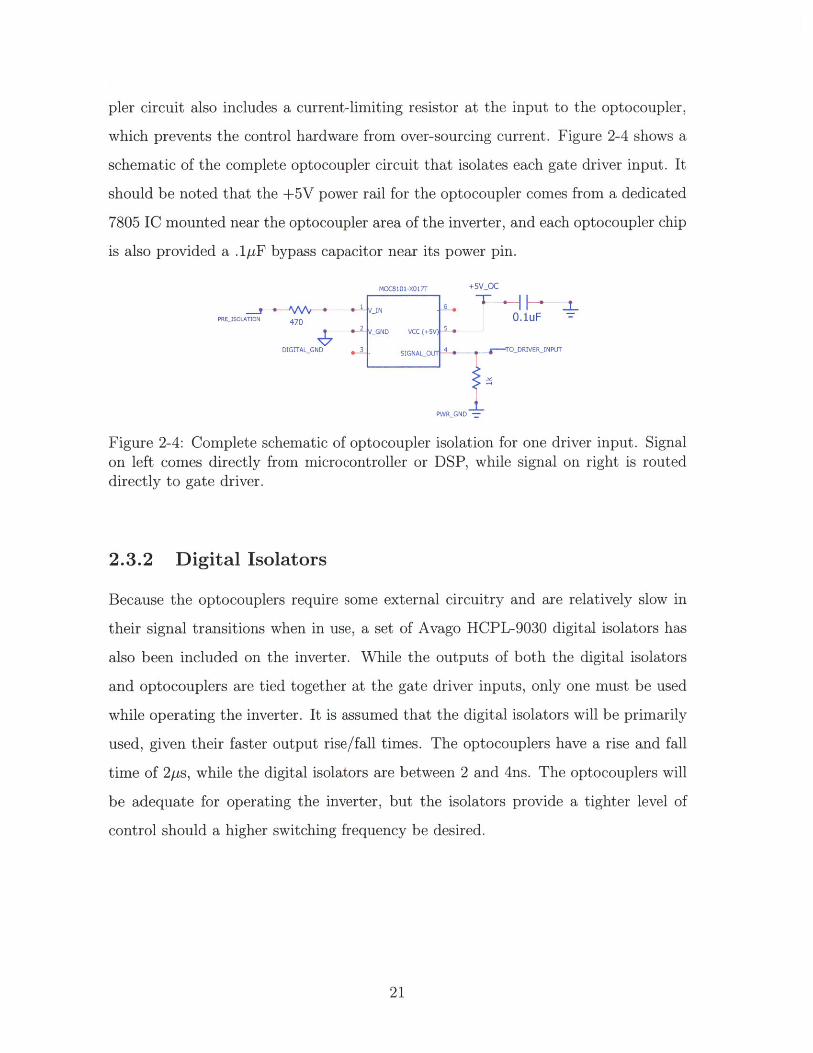
pler circuit also includes a current-limiting resistor at the input to the optocoupler,
which prevents the control hardware from over-sourcing current. Figure 2-4 shows a
schematic of the complete optocoupler circuit that isolates each gate driver input. It
should be noted that the +5V power rail for the optocoupler comes from a dedicated
7805 IC mounted near the optocoupler area of the inverter, and each optocoupler chip
is also provided a .1pF bypass capacitor near its power pin.
MOC8101-XOS7r +5VOC
__Y.. *-AtAv- 1 O_1luF-PRE ISOLATION 470 0.1uF
SVGND VCC (+5V)
DIGITAL GND 3 SIGNALOUT --- __ --- TODRIVERINPUT
PWRGND =
Figure 2-4: Complete schematic of optocoupler isolation for one driver input. Signalon left comes directly from microcontroller or DSP, while signal on right is routeddirectly to gate driver.
2.3.2 Digital Isolators
Because the optocouplers require some external circuitry and are relatively slow in
their signal transitions when in use, a set of Avago HCPL-9030 digital isolators has
also been included on the inverter. While the outputs of both the digital isolators
and optocouplers are tied together at the gate driver inputs, only one must be used
while operating the inverter. It is assumed that the digital isolators will be primarily
used, given their faster output rise/fall times. The optocouplers have a rise and fall
time of 2ps, while the digital isolators are between 2 and 4ns. The optocouplers will
be adequate for operating the inverter, but the isolators provide a tighter level of
control should a higher switching frequency be desired.
21

The digital isolators are much simpler to use as well, as seen by their complete
circuit schematic in Figure 2-5. The optocouplers remain a part of the inverter topol-
ogy as a failsafe, so that control signals may still be isolated and sent to the gate
driver in the event that one of the digital isolators fails.
+5VDIIN +5VDIOUT
47nF 47nF ~HCPL-9030
;± DD1 VDD27PRE_IN2_DI. 3- -IN1-OUTHININ2 OUT2.--ii
PREIN1_DI GNDN GND2
4? '=PWR_GNDDIGITALGND
Figure 2-5: Each digital isolator chip is capable of isolating two independent signals,and has an overall less complex footprint.
2.3.3 Grounding
Because of the various isolated sections necessary for the board to operate with suf-
ficient protection for the control and measurement hardware, there are five separate
'grounds' used on the inverter, all completely separated from each other on the phys-
ical board. First, the inverter analog ground provided by the DC/DC converter's
OV output is isolated from the DC wall supply ('wall ground') as previously men-
tioned. However, as the gate driver operates on the three-phase bridge between the
high voltage PV array and its own common level, COM, the power supply for the
gate driver must be relative to a separate power ground, with both this power ground
and COM connected to the driver chip through a trio of sensing resistors. This can
be seen back in Figure 2-3, the typical IR21362S connection. This extra isolation
between the main inverter power supply and the gate driver power is done through
another DC/DC converter, a TI DCP010515. Finally, the digital drive signals from
the microcontroller/DSP are also isolated through either the optocoupler or digital
isolator circuit as mentioned in the previous section. These drive signals are relative
to another, unique, digital ground. Note that the digital and analog grounds should
be connected together via a single wire when using the inverter. They are explicitly
22

separated on the circuit design but connect at a single intersection to reduce unwanted
noise, as is common in circuit design. Table 2.1 presents a concise view of the various
grounds and the modules that relate to them.
Wall ground wall-plugged DC source used for board powerCOM wall-plugged high voltage DC source modeling PV arrayPower ground driver IC, optocoupler/isolator outputAnalog ground voltage/current sensors, signal processing unitsDigital ground optocoupler/isolator input, microcontroller/DSP
Table 2.1: List of grounds used and circuit modules relative to them.
2.4 Signal Measurement
As the inverter is designed to operate as a module within the microgrid, it is necessary
to include measurement hardware to monitor various voltage and current levels on
the board; these measurement signals are read by monitoring boards throughout the
microgrid and sent to the main LabVIEW interface for control purposes. While there
are several spots on the inverter for measurements to be made, this section discusses
the design of the voltage sensor and current sensor circuits. The discussion of the
locations of the the actual sensors is presented in Chapter 3.
2.4.1 Voltage
The voltage sensor used in the inverter is the LEM LV 20-P, which draws a minimal
amount of current (10 mA) while remaining capable of measuring up to a 500V
difference between its input terminals. It does require two external resistors - one
resistor between the high voltage to be measured and high input pin, and one resistor
at the measurement output pin. The high voltage resistor presents some difficulty -
ideally, it should be a precision resistor with a tolerance of ±1% in order to provide
accurate measurements. Sufficiently high power-rated precision resistors that can
dissipate the necessary heat are not common, but the Riedon PF1262-20K 20kQ
precision resistor is capable of dissipating up to 20W with an adequate heat sink
23

affixed to it. Figure 2-6 shows the general schematic for each of the voltage sensors
placed on the inverter board.
LV 20-P
+15Vlow
4
-2 -/ MEASURED
V- f-
oFigure 2-6: Circuit used for voltagesensing throughout the inverter board.V- does not necessarily need to begrounded.
2.4.2 Current
The Allegro ACS712 current sensors used in the inverter board require some very
minor supplementary components to operate as well. An external capacitor is used
to set the device bandwidth; for the microgrid measurements a capacitance of lnF
is adequate, as seen in Figure 2-7. The primary difficulty with the current sensor
is its need to be physically close to the copper traces being measured, which proved
challenging given the wide power traces necessary on the inverter.
+5V_IS
c>
ACS712ELCTR-30A-T
1 i+ vC2+ VOU'T I
P2- FILTER 5
V+_AFTERSENSING __ P1- GNC U
Figure 2-7: Circuitused for current sensingthroughout the inverterboard. The tracesmust be routed directlythrough the sensor IC.
24

2.5 Signal Processing
The final circuitry designed for the inverter is related more to interfacing with the
microgrid system than the inverter itself. The digital measurements being output by
the various sensors are between ±2.5V, but must be shifted to levels between OV and
+5V in order to be processed by the external microgrid monitoring hardware. Note
that these signals are still analog as they are precise measurements, not digital control
logic. To accomplish this, six separate signal processing units have been included in
the inverter design, with their inputs and outputs made easily accessible via screw
terminal blocks for any external signal to be processed. Each unit is a TL071 op-amp
in a summing amplifier configuration, with a -5V reference level at one input and
the measurement signal to be shifted at the other. The summing amplifier follows
equation 2.1
Vou = Rfeedback x (Vin - 5V) (2.1)
For example, an input signal of -2.5V would be altered to +3.75V for further pro-
cessing by the microgrid. An LC output filter and damper is also included, although
these are all very small surface mount components, unlike the filter and damper de-
signed for the power stage. The -5V reference level is set using an AD588 voltage
reference. Figure 2-8 on the following page presents both the voltage reference circuit
and an example signal processing unit.
25

AD588ARWZ
+5V_REF - A3 C TU -V 5- V_REF+VS N A-4 OUT FORCE
4 A3 aUT SENSE A4 OUT SENSE 13A 3 IN A4 IN 12 ,
SAIN AD3 BAL AD]|HIGH VCT 1 1
\)ISE REJE GNU SENSE -INVLOW GND SENSE +N
30k
Figure 2-8: Top: one of six summing amplifier configurations. used to shift signals upby +5V.Bottom: Voltage reference circuit used to create steady -5V. Because minimalcurrent is drawn by the summing amplifiers, all share the same -5V reference.
26
+ 15VT,
50k
I ~---±
Ak
TL071D
-'GNLI- OSTRIM 011IRM - INLOT-* 4 N+ V+.5+
AkV NC --
-SV REF
-15v +15 V
72k__-
47T
_T
-

Chapter 3
Final Layout
3.1 Physical Footprint
Figure 3-1: Overall view of circuit footprint. The ground planes are hidden in thisview of the board.
The final circuit measures 12in wide by 10in tall and uses 4 total layers. One
layer is reserved exclusively for ground planes to reduce noise, especially around the
27

MOSFETs and filters. There were several concerns when laying out the physical
circuit. Most importantly, the traces handling the three-phase bridge and its output
filters needed to be capable of handling up to 10A. It was conservatively calculated
that these traces should have a width of at least 0.5in, although they are narrower
at certain areas to route around the MOSFETs and current sensors. All control
traces are 0.015in, while individual component power traces are 0.02in wide in order
to distinguish them. All components which use heat sinks have had the heat sinks
included in the design to accommodate for spacing.
To optimize switching speed and try to match any delays across all MOSFETs, the
driver chip is mounted on the underside of the board, directly underneath the middle
of the second phase of the totem bridge. This central location allows its gate drive
outputs to be directed to the switches without the use of any vias or long, undesirable
trace loops. The low-power control routes and circuit modules are placed on the top
and right sides of the board, allowing for quick access to a wide assortment of I/O
screw terminals while maintaining separation from the high-power area.
28

Figure 3-2: View of three separate ground planes in circuit. Component footprintsare shown for reference.
The ground planes are shown in Figure 3-2. The largest plane exists under the
entire high-power section as this will be most susceptible to noise. The top right
plane lies below the digital inputs coming from the control hardware, and finally
the rightmost plane is designed to ground all analog signals - the sensing and signal
processing components. The digital and analog grounds should be connected through
the use of the board's screw terminals that follow the top and right borders of the
inverter. This single-point connection prevents any internal loops from being created
in the trace, which would create unnecessary parasitic inductance.
29

3.2 Conclusion
The three-phase bridge is a common topology and further details of the inverter, such
as certain component values, are dependent on the control scheme used to switch the
MOSFETs. The inverter designed in this paper is intended to general purpose, and
the finalized overall schematic is appropriate for any practical control scheme that may
be used in the microgrid. The switching hardware and interface software discussed in
Chapter 1 still remains in use and has proven to be both quick and intuitive to use,
as originally intended. Though the microgrid itself is an ongoing project, the inverter
itself has been developed to accommodate this in anticipation of future changes in
the project.
30

Bibliography
[1] A. H. Kasem Alaboudy, H. H. Zeineldin, and J. Kirtley. Impact of DG InterfaceControl, Microgrid Control Strategy and Load Type on Microgrid Stability, MasdarInstitute of Science and Technology and MIT. 2011.
[2] IEEE. 1547.2: IEEE Application Guide for IEEE Std 1547 IEEE Standard forInterconnecting Distributed Resources with Electric Power Systems, chapter 8.1.5.2009.
[3] Jared Monnin. Impact of Load Type on Microgrid Stability. Master's thesis, MIT,2010.
[4] John G. Kassakian, Martin F. Schlecht, and George C. Verghese. Principles ofPower Electronics, chapter 24.1. Addison-Wesley, 1991.
[5] International Rectifier. IR213 3-Phase Bridge Driver Data Sheet No. PD60166rev U. 2008.
[6] James Worden and Michael Zuercher-Martinson. "How Inverters Work". SolarProMagazine Issue 2.3, Apr/May 2009.
31