Embed Size (px)
Citation preview

DESIGN AND DEVELOPMENT OF EMBEDDED
DSP CONTROLLERS FOR POWER
ELECTRONIC APPLICATIONS
by
RAMAN NAIR HARISH GOPALA PILLAI
Presented to the Faculty of the Graduate School of
The University of Texas at Arlington in Partial Fulfillment
of the Requirements
for the Degree of
MASTER OF SCIENCE IN ELECTRICAL ENGINEERING
THE UNIVERSITY OF TEXAS AT ARLINGTON
May 2006

ii
ACKNOWLEDGEMENTS
I am extremely grateful to my supervising professor Dr Babak Fahimi for his
unstinted support. His guidance and encouragement has been vital in my learning
process. I am thankful for his confidence in me and mentoring me for the successful
completion of this thesis.
I would like to express my gratitude to my parents and sisters for their
unbounded care and love. Their encouragement was extremely valuable to me.
Furthermore I am thankful to Dr Rasool Kenarangui and Dr Wei-Jen Lee for willing to
be on my supervising committee.
I would also like acknowledge my friend Pallavi for her time and valuable
feedback. My appreciation also extends to Ranjit, Mahesh and other members of PECM
lab for their help in completing this thesis.
April 18, 2006

iii
ABSTRACT
DESIGN AND DEVELOPMENT OF EMBEDDED
DSP CONTROLLERS FOR POWER
ELECTRONIC APPLICATIONS
Publication No. ______
Raman Nair Harish Gopala Pillai, M.S.
The University of Texas at Arlington, 2006
Supervising Professor: Babak Fahimi
Power applications like motor drives, inverters have complex algorithms that
can be used to improve their efficiency. More often reduced manufacturing cost takes
precedence over better efficiency. DSPs with their high computational power can
provide reduced cost and higher efficiency. Though the cost of a standalone DSP chip
has reduced, its integration to form a complete embedded product is an area often
overlooked. High frequency of operation, reduced package size, and sensitivity to

iv
component placement are some of the factors that affect the interface between
input/output devices and the DSP.
This thesis presents the design and development of an embedded DSP controller
board using TI’s TMS320F2808. A three phase Space Vector PWM inverter is
constructed and used to test the DSP board. This thesis also compares Space Vector
PWM with other carrier based modulation schemes.

v
TABLE OF CONTENTS
ACKNOWLEDGEMENTS................................................................................... ii ABSTRACT ......................................................................................................... iii LIST OF ILLUSTRATIONS................................................................................. viii LIST OF TABLES ................................................................................................ xii Chapter 1. INTRODUCTION …….. .......................................................................... 1 1.1 Overview of DSP ….. .......................................................................... 1 1.2 Timeline: DSP Processors……….. ...................................................... 6 1.3 Digital Signal Controller ...................................................................... 10 1.4 Need for DSP controllers or Digital Signal Controllers in power and motor control applications.................................................. 12 2. HIGH SPEED PRINTED CIRCUIT BOARD DESIGN ............................ 19 2.1 Overview of PCB Technology......................................................... 19 2.2. Surface Mount Technology ............................................................ 21 2.3 High Speed PCB Design ................................................................. 28 2.3.1 Transmission line analysis of PCBs ....................................... 29 2.3.2 Lattice diagram method for transmission line analysis ........... 34 2.3.3 How to avoid reflections?...................................................... 38

vi
2.3.4 PCB design with EMI/EMC considerations ........................... 43 2.3.5 Introduction to OrCAD Capture and Layout .......................... 62 3. THREE PHASE INVERTER .................................................................... 64 3.1 Three phase inverter: Working ........................................................ 64 3.2 Pulse Width Modulation (PWM) ..................................................... 68 3.3 Space Vector Pulse Width Modulation (SVPWM)........................... 69 3.4 Sinusoidal modulation and third harmonic injection ........................ 76 3.5 Comparison of Space Vector and Sinusoidal PWM techniques........ 80 4. RESULTS……………….......................................................................... 85 4.1 High speed printed circuit board...................................................... 85 4.1.1 Creation of schematic ............................................................ 85 4.1.2 Component selection, design of footprints ............................. 85 4.1.3 Component placement ........................................................... 88 4.1.4 Number of layers and size of board........................................ 88 4.1.5 Circuit analysis for transmission line effects .......................... 88 4.1.6 Routing…….......................................................................... 92 4.1.7 Preparation of gerber files, fabrication, assembly and testing............................................................................. 92 4.2 Three phase inverter ........................................................................ 94 4.3 Simulation results ........................................................................... 95 4.4 Experimental results ........................................................................ 98 4.5 Comparison of SVPWM, SPWM and SPWM with one sixth third harmonic …........................................................................... 98

vii
5. CONCLUSIONS AND FUTURE WORK................................................. 102 5.1 Conclusions……... .......................................................................... 102 5.2 Future work …….. .......................................................................... 103 Appendix A. DSP BOARD SCHEMATICS AND LAYOUT ......................................... 104 B. BILL OF MATERIALS............................................................................ 117 C. SIMULINK SPACE VECTOR PWM BLOCK DIAGRAM...................... 121 D. THREE PHASE INVERTER SCHEMATICS .......................................... 126 E. SPACE VECTOR PWM CODE ............................................................... 129 REFERENCES ..................................................................................................... 140 BIOGRAPHICAL INFORMATION..................................................................... 145

viii
LIST OF ILLUSTRATIONS
Figure Page 1.1 FIR filter ...................................................................................................... 2 1.2 Simplified diagram of a conventional DSP processor ................................... 7 1.3 Graphical representation of processor complexity......................................... 9 1.4 Block diagram of TMS320C28X Digital Signal Controller architecture ....... 11 1.5 Comparison of clock speeds of various Digital Signal Controllers ................ 16 1.6 Comparison of Flash and RAM memory of various Digital Signal Controllers............................................................................. 16 1.7 Comparison of ADC conversion times of various Digital Signal Controllers............................................................................. 17 2.1 Typical six layer PCB .................................................................................. 19 2.2 Package weight comparison of surface mount devices (chip carriers)
with THM devices........................................................................................ 23 2.3 Comparison of package area with THM (DIP) and surface mount devices (SOIC, PLCC) ................................................................................. 23 2.4 Three types of surface mount assemblies ..................................................... 26 2.5 Comparison of signal output at load with two drivers with different rise/fall times................................................................................................ 28 2.6 Wave moving from lower impedance medium to higher impedance............. 30 2.7 Wave moving from higher impedance medium to lower impedance ............. 31 2.8 Surface Microstrip........................................................................................ 32 2.9 Embedded Microstrip ................................................................................... 32
ix
2.10 Stripline ....................................................................................................... 32 2.11 Dual Stripline............................................................................................... 32 2.12 Lumped approximation of a transmission line .............................................. 33 2.13 Transmission line effects.............................................................................. 35 2.14 Simplified representation of a transmission line............................................ 36 2.15 Analysis of incident and reflected wave........................................................ 36 2.16 Lattice diagram ............................................................................................ 37 2.17 Types of termination .................................................................................... 39 2.18 Rising and falling edges of 5V CMOS circuit showing effect of series termination ......................................................................................... 40 2.19 A Thevenin Network used as pullup for a TTL bus ...................................... 41 2.20 Differential and common mode currents....................................................... 44 2.21 Conventional representation of differential and common mode currents ....... 45 2.22 Basic antenna design .................................................................................... 46 2.23 At low frequencies current follows path of least resistance ........................... 46 2.24 At high frequencies current follows path of least inductance ........................ 47 2.25 Distribution of high frequency current density underneath a signal trace ...... 47 2.26 Routing a trace over a slot in a plane can cause large loop area..................... 48 2.27 Comparison of trace length with number of layers in a PCB......................... 50 2.28 PCB layer stackup 1 ..................................................................................... 51 2.29 PCB layer stackup 2 ..................................................................................... 52 2.30 Functional distribution of the custom DSP board.......................................... 53

x
2.31 Trace and ground current in split and single ground planes........................... 54 2.32 Equivalent circuit of decoupling capacitor ................................................. 55 2.33 0603 ceramic capacitor impedance vs frequency (C=1uF, ESR=12mΩ, ERL=2nH) ................................................................................................... 56 2.34 Self resonant frequencies of capacitors vs logic families with 0.25’ leads ..... 57 2.35 Equivalent circuit of decoupling capacitor with the equivalent PCB capacitance .......................................................................................... 58 2.36 Impedance at parallel resonance versus ESR (1uF 0603 ceramic) ................. 59 2.37 Test performed on TI ABT541, Vcc line disturbance versus capacitor size at different distances.............................................................................. 61 2.38 Schematic view of a circuit in OrCAD Capture ............................................ 63 3.1 Three phase inverter with balanced load....................................................... 65 3.2 Switching states of a three phase inverter ..................................................... 66 3.3 Equivalent circuit with switch sequence ....................................................... 67 3.4 PWM switching strategy based on turn ON times......................................... 70 3.5 Representation of 3 phase signals in dq reference frame ............................... 71 3.6 Switching pattern of space vectors................................................................ 73 3.7 Switching time instants of Sa, Sb and Sc ...................................................... 75 3.8 Sinusoidal Pulse Width Modulated signal..................................................... 77 3.9 Comparison of line to neutral and line to line voltages.................................. 78 3.10 Line to line voltage with 3rd harmonic injected in the line to neutral voltage.............................................................................................. 79 3.11 Comparison of phase modulating signals...................................................... 81 3.12 THD for four PWM strategies ...................................................................... 83

xi
4.1 Flowchart of PCB design process ................................................................. 86 4.2 Continued-Flowchart of PCB design process................................................ 87 4.3 Functional distribution of the DSP board...................................................... 88 4.4 PCB layer stackup........................................................................................ 89 4.5 PSPICE simulation and lattice diagram method using Excel, without series termination ............................................................................ 91 4.6 PSPICE and Excel simulations with series termination................................. 91 4.7 Completely routed PCB................................................................................ 92 4.8 XCLKOUT in the output of the custom DSP board after initial powerup...... 93 4.9 Output of custom DSP board generating PWM signals ................................. 93 4.10 RC circuit used to filter SVPWM signals...................................................... 96 4.11 SIMULINK model of 3 phase SVPWM with filter block.............................. 96 4.12 SVPWM line to neutral voltages .................................................................. 97 4.13 SVPWM line to line filtered waveforms....................................................... 97 4.14 FFT of SVPWM (SIMULINK) line to line voltage (Vab) .............................. 98 4.15 Filtered line to neutral voltage Van from 3 phase inverter............................. 99 4.16 Filtered line to line voltage Vab from 3 phase inverter...................................99 4.17 Comparison of THD of SVM, SPWM and SPWM with one sixth 3rd
harmonic fc/fo=10kHz/100Hz=100..............................................................100

xii
LIST OF TABLES
Table Page 1.1 MCU, DSP and DSC comparison................................................................. 11
1.2 Comparitive study of various algorithms ...................................................... 14
1.3 Comparison of currently available Digital Signal Controllers ....................... 15 2.1 Termination types and their placement ......................................................... 42
2.2 Comparison of series resonant frequency of Thru Hole and Surface Mount capacitors ............................................................................. 57
3.1 Switching patterns in a 3 phase inverter........................................................ 68 3.2 Switching patterns with Vd, Vq and Vdq voltages........................................ 72 3.3 Switching time instants of each sector .......................................................... 76

1
CHAPTER 1
INTRODUCTION
1.1 Overview of DSP Processors
“DSP processors” may be defined as “microprocessors designed to perform
digital signal processing” [1]. Over the years microprocessors have been used to
perform complex computations with speed being the primary focus. Size and memory
were never constraints in advanced microprocessor based systems. On the other hand
microcontrollers, which are again derivatives of the microprocessor family, were
designed for applications that had relatively simple computations, low memory
requirements and extreme sensitivity to size. On the outset, DSP processors fall in
between these two.
Architectural properties of conventional DSP processors:
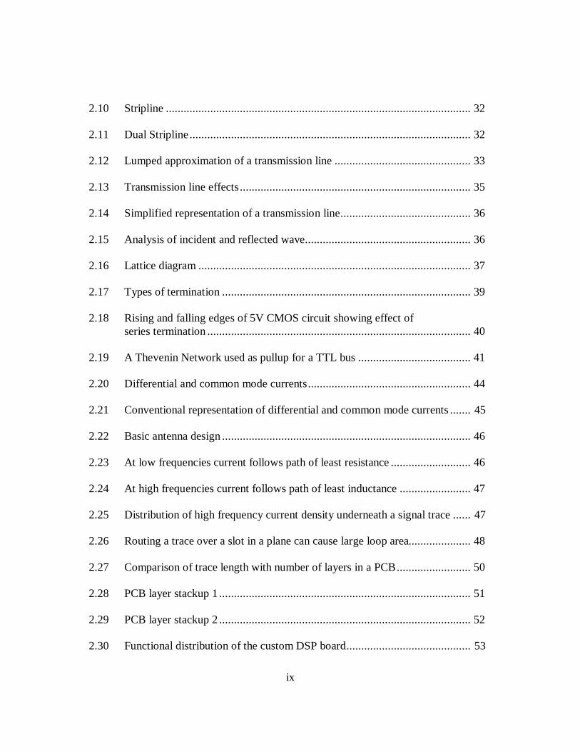
1) Multiply and accumulate or MAC: Any digital logic implemented in
hardware is usually faster than its corresponding software equivalent. This is one of the
basis for ASIC (Application Specific Integrated Circuit). DSP processors have evolved
based on DSP applications. Sum of products terms (∑ xy ) are one of the most
frequently used operations in DSP. FIR filter, IIR filter, convolution and Fourier
transforms are few examples [2]. In all of these examples multiply-accumulate or a
“MAC” operation as it popularly known is the common factor. Though DSP processor
architectures have mutated over the years, “historically” one of the fundamental features
2
that differentiate it from general microprocessor is its support for single cycle MAC
operations in hardware. An FIR (Finite Impulse Response) filter illustrated in Figure 1.1
can be defined by the following equation
∑−
=−=
1
0
)()(N
kk knxany (1.1)
where y(n) represents the output response,
ak: is the filter coefficient,
x(n-k) represents the kth delayed input sample.
From this expression we find that the output is equivalent to a sum of products
(SOP). Hence in order to speed the process of computation, DSP processors have a
multiplier and accumulator unit implemented in hardware.
Figure 1.1 FIR filter
2) Memory organization and access: Conventional general purpose processors
(GPPs) have a single bus to transport data and program instructions between memory
and the processor (Von Nuemann architecture). Since programs in DSP applications and

3
most embedded applications are static (which means the program size is deterministic
and usually designed for a specific application), better performance is achieved by
having separate buses to access instructions and data from memory (Harvard
architecture). The above property is characteristic of microcontrollers too. Since most
data input in DSP applications is sequentially organized, memory access in DSP
processors is improved by having specialized hardware to increment memory address
pointers as well as support for specialized addressing methods like register indirect
addressing with auto-increment. “Circular addressing” is another addressing mode
characteristic of DSP processors, where in the memory address pointer automatically
wraps around to the beginning address after a predefined set of memory accesses. As
seen in the FIR filter equation above, the memory access to filter coefficients possess
this circular pattern. In order to further speed up memory access, some DSP processors
have multiple memory banks with separate buses. But since, this requires more chip
space and power, the number of memory buses is limited. DSP processors tend to
improve memory access by means of memory parallelism. In contrast, GPPs improve
memory access using cache memory. Cache memory is small high speed memory
closest to the processor. The objective is for the processor to always or most of the time
access data/program from the cache. Implementation of cache is based on probabilistic
theory and is bane for real time systems which require deterministic timing constraints.
Since DSP processors more often deal with hard real time systems (systems with strict
timing constraints), cache strategy is usually not implemented. As will be seen later,
some DSP processors implement an instruction cache alone to aid looping.

4
3) Arithmetic format: Numbers are represented either as fixed point or floating
point in all processors. In fixed point, as the name suggests, the binary point is placed at
a fixed location within the data word resulting in a fixed range (usually between -1 and
+1). On the other hand in floating point representation a number is represented in the
form mantissa x 2 exponent, the binary point is allowed to “float” according to the value of
the exponent. Floating point representation has a higher dynamic range (ratio between
the highest and smallest number) compared to fixed point. Intuitively DSP processors
must favor floating point representation. But cost, size and power consumption of
floating point hardware restrict its implementation. The lower end of the latest DSP
processors being cost sensitive has fixed point representation. This places onus on
programmers to understand the requirements of the application and perform scaling
operations in software to overcome limitations of fixed point representation.
4) Specialized Instruction set: As seen above, DSP processors have hardware to
perform multiple operations in a single cycle, which effectively means a single
instruction performs more than one task. For example consider instruction from TI’s
TMS320C24X series.
MACD pma,dma (multiply and accumulate with data move)
pma – program memory address; dma – data memory address. (Advantage of
Harvard architecture can be seen here, with simultaneous access to two memory banks
being possible in a single instruction cycle)
This instruction does the following:
1) Move PC (Program counter) -> MSTACK (stack).

5
2) Move pma -> PC.
3) ACC (Accumulator) + shifted PREG (product register) -> ACC.
4) (dma) ->TREG (temporary register)
5) (dma) x (pma) ->PREG (product register)
6) Increment dma.
It is apparent from this instruction that the DSP with multiple execution units is
capable of performing multiple operations in a single instruction. With the need to have
small programs, DSP processors are designed to have a relatively small instruction set.
The number of register based instructions (common in GPPs) is reduced and more
information is encoded within the opcode of the instruction. Hence most DSP
processors possess a specialized and irregular instruction set. This does not ease
programming, requiring programmers to have a complete understanding of assembly
language. Most DSP processor manufacturers provide C language support, but the
general trend towards efficient programming is to fine tune in assembly.
5) Zero-overhead looping: Going back to the FIR filter diagram above, we find
that the operation is iterative with a fixed number of coefficients operating on a set of
input samples in a loop. If implemented on a conventional GPP, few extra cycles would
be spent on the loop test condition. For example consider the instruction JZ belonging
to the 8086 instruction set. This instruction consumes 4 clock cycles when there is no
jump and 13 clock cycles for a jump. DSP processors have a specialized hardware to
circumvent this problem. The term zero-overhead looping means that the processor can
execute loops without consuming cycles to test the value of the loop counter. [3]. Hence

6
even loop instructions effectively take a single instruction cycle due to this extra
hardware implementation.
1.2 Timeline: DSP Processors
DSP processors have grown rapidly over the years, to such an extent that few of
the properties considered essential to a conventional DSP processor are missing. For
example the TI’s TMS320C62XX which is considered one of the better DSP processors
in the current era does not have “zero overhead looping” feature [2]. With more
applications like motor control, power supplies embracing DSP technology, the current
trend in DSP architecture may be broadly split into three categories:
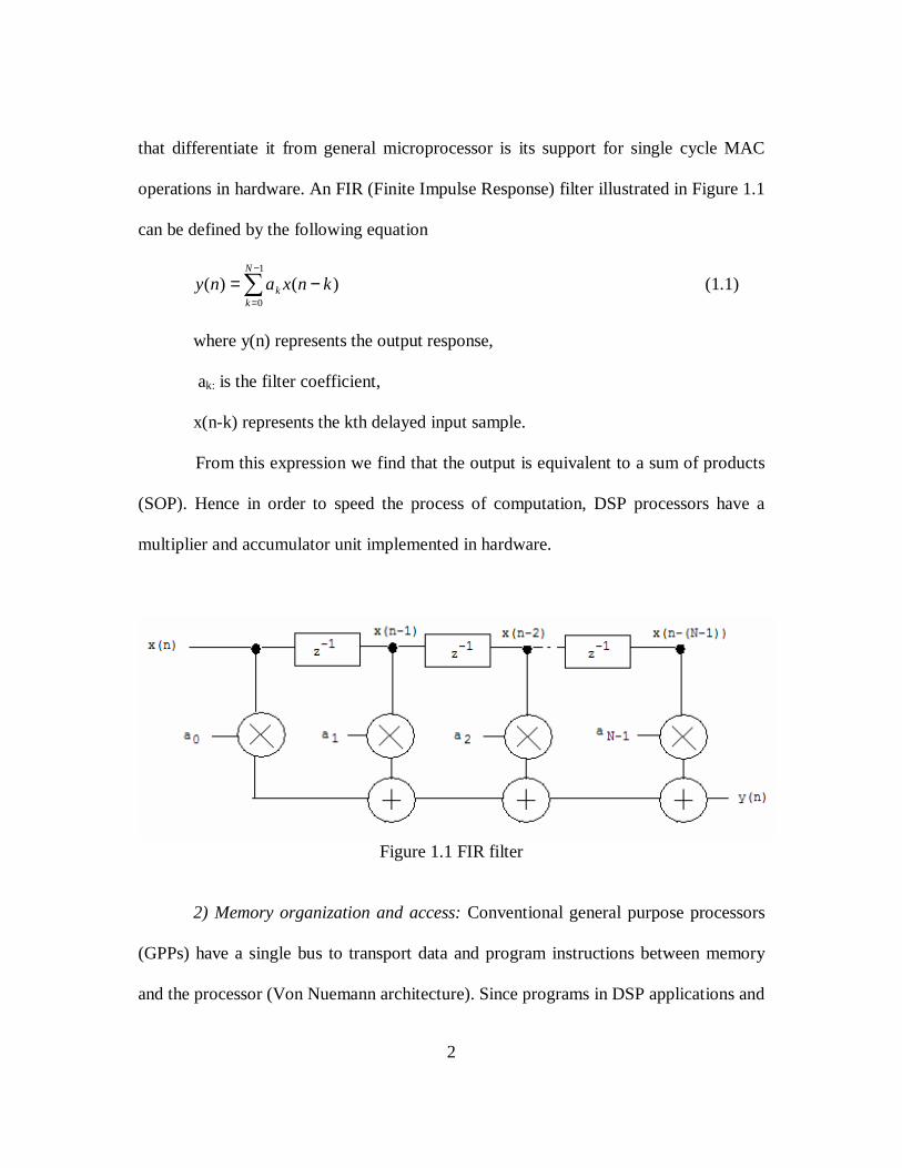
1) Conventional or first generation DSP processors: These processors have
most of the properties typical of a conventional DSP processor described above. The
focus in this category of processors has been on cost and integration of peripheral units
like Analog to Digital Converter, Serial Peripheral Communication (SPI) and Pulse
Width Modulation (PWM) unit. They can compute 20-100 Millions Instructions Per
Second (MIPS), which is sufficient for motor control, digital power supplies,
automotive and consumer applications. This generation of processors, though initially
designed for signal processing applications have gradually mutated towards control
applications and are better known DSP controllers or Digital Signal Controllers (DSC).
This thesis delves into this category of processors and will be explained in later part of
this chapter. Examples of these DSP processors include Freescale’s DSP56XXX series
7
and TI’s TMS320C2XXX series. Figure 1.2 shows the diagram of conventional DSP
processor [4].
Figure 1.2 Simplified diagram of a conventional DSP processor
2) Enhanced conventional or second generation DSP processors: Increasing
clock speed is one of the straight forward ways of improving speed of computation. But
this comes at the expense of higher power dissipation, size and higher costs. One other
way is to increase parallelism in the design by having multiple arithmetic units (AU),
multiple memory ports and efficient address generation hardware [5]. Recent
developments in fabrication techniques and use of lower voltage switching levels have
reduced power dissipation and overall cost. There is very thin line of distinction
Program Bus
Data Bus
Program Memory
Data Memory
Control
Adder
Accumulator
Multiplexer Multiplexer
Multipl ier

8
between the first and second generation processors. From a broad perspective, this
generation of processor can be considered an “enhanced” [2] version of their
predecessor. For example Lucent DSP16xxx processors have two MAC units, a 32-bit
data bus and 8 accumulators in comparison to its first generation processor DSP16xx
series having one MAC, 16-bit data bus and two accumulators. TI’s TMS320C5xxx
series are another set of processors in this category which address needs of wireless
modems, cell phones, GPS receivers and, digital audio players.
3) Multi-issue or Third generation DSP processors: Conventional DSP
processor architecture is unfavorable to high level programming due to its irregular
specialized instruction set. For this generation of processors, with speed of computation
being the primary objective, DSP architects felt the need to borrow solutions from
advanced GPP designs. High end applications like image processing required efficient
programming tools in addition to fast computation. Two technologies currently used
among these processors are VLIW (Very Long Instruction Word) and superscalar. In
both these designs, the processor executes a group of instructions in parallel. The two
designs differ in the order in which the instructions are executed. VLIW is more
predictable with the order being determined when the program is assembled and does
not change at runtime. On the other hand superscalar have specialized hardware to
determine the order of instruction execution based on data dependencies [2]. This
means that same set of instructions may be grouped differently by the processor when
run at different occasions. This unpredictability is not favorable for real time DSP
applications which have stringent time deadlines. This is one of the reasons for VLIW

9
being more popular among most manufacturers in this category. Another concept
prevalent among both these architectures presented above is SIMD (Single Instruction
Multiple Data). As the name suggests, the processor is designed to operate on different
data for the same instruction. This can significantly improve throughput for algorithms
that process data in parallel. For example in the FIR filter example above, the same
MAC operation is performed on different sets of input data and hence more work is
done when different data is presented to multiple executions units for the same
instruction. DSP processors in this generation are characterized by larger data buses,
higher clock frequencies, large number of execution units and a sophisticated control
unit to synchronize data flow among the parallel units. Hence these processors are much
more expensive, dissipate more heat and occupy more space than their predecessors.
Examples of DSP processrs in this category are TI’s TMS320C6xxx series which
operates at almost 1.1Ghz, Analog Devices TigerSHARC and StarCore (built under
partnership between Motorola and Lucent).
Figure 1.3 Graphical representation of processor complexity

10
1.3 Digital Signal Controller
Microcontrollers used to rule the roost for over a decade in almost all embedded
control applications. They are known for their small size, efficient input-output
communication ports and ability to perform real time control tasks. Some of their major
applications include motor control, power converters and consumer electronics like disk
drives and music players. During the same era, DSPs also co-existed and were mainly
used in telecommunication, image processing and other number crunching applications.
Complex control algorithms like vector control have existed for a while on paper, but
never used commercially due to the lack of cost effective and fast microcontrollers.
DSP manufacturers began to include more controller related features like on chip
memory and peripheral units. Similarly microcontroller manufacturers tried to improve
performance by increasing the data bus size from 8 to 16 bits. DSP processors that had
controller abilities were called DSP controllers. In 2002, Microchip officially coined the
term “Digital Signal Controller or DSC” [6]. Since then other companies have
recognized the mergence. (like TIs TMS320C2000 series and Freescales 56800E
series). Based on the evolution of DSPs mentioned above, DSCs may be placed in the
first generation of DSPs. Figure 1.4 depicts the block diagram of the TMS320C28X
digital signal controller [11].
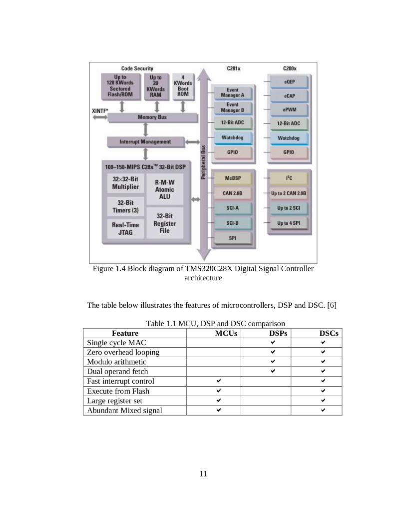
11
Figure 1.4 Block diagram of TMS320C28X Digital Signal Controller
architecture The table below illustrates the features of microcontrollers, DSP and DSC. [6]
Table 1.1 MCU, DSP and DSC comparison Feature MCUs DSPs DSCs
Single cycle MAC
Zero overhead looping
Modulo arithmetic
Dual operand fetch
Fast interrupt control
Execute from Flash
Large register set
Abundant Mixed signal

12
1.4 Need for DSP controllers or Digital Signal Controllers in power and motor control applications
DSPs were initially designed specifically for signal processing algorithms. With
the focus shifting to cost effectiveness and efficiency, more control applications started
utilizing the advantages of DSPs. Whether DSPs actually help control applications is
not completely obvious. For some applications a high speed microcontroller with a
larger data bus might help in faster computation. The need for DSP may be justified by
considering the similarities between control and signal processing algorithms. Consider
for example the PI controller. The transfer function in continuous time domain is
represented by the equation [7]
)()( sIs
KKsU i
p
+= (1.2)
where U :controller output signal
I : input error signal
s : Laplace variable
Kp: proportional gain
Ki: integral gain
The above equation in discrete time domain may be represented by the following
expression
pzi
pzi
kkkk
KTK
AandKTK
Awhere
UIAIAU
−=+=
++= ++
22 01
0111
(1.3)

13
From the above expression we find that the output is Sum of Products (SOP),
which is favorable for DSP operation. Intuitively most continuous domain systems
when converted to discrete domain form a system of difference equations. Hence most
control algorithms can take advantage of DSP processors. Table 1.2 [10] provides a
comparative study of computation time requirements of various algorithms.
In power electronics applications, DSP or DSCs are used to replace hardware
component by performing the equivalent operation in software. Power conversion
devices like DC-DC converters, DC-AC inverters operate by controlling switches at
high frequency. Hence higher order harmonics are inevitably present in the output
signal. Traditionally external hardware was used to perform the filtering operation. Now
with the power of DSC, the filtering operation can be accomplished in software.
In motor control applications, DSC plays a significant role in improving
efficiency, reliability and reducing manufacturing costs. Control routines like Field
Oriented Control (FOC) have several matrix routines which are again MAC operations.
Switched Reluctance (SR) motors are known for they low manufacturing cost, high
reliability and excellent torque characteristics [9]. But control of these motors was
difficult since it required precise excitation of the stator windings with respect to rotor
position. With the help of DSC, rotor position could be estimated in real time by
modeling the motor in software.
DSCs usually provide a bandwidth of 20 to 150 MIPS [8]. Motor control
typically requires 20-40 MIPS. This leaves sufficient room for performing auxiliary
functions in white good appliances like voice recognition, implementing networking

14
and wireless protocols. Hence use of DSC can reduce the size and cost of the overall
system.
Table 1.2 Comparative study of various algorithms Function Cycle Count
Equation Conditions Number
of cycles Execution time @ 40MIPS
Complex FFT** - N=64 3739 93.5µs Complex FFT** - N=128 8485 212.1µs Complex FFT** - N=256 19055 476.4µs Single Tap FIR - - 1 25ns Block FIR 53+N(4+M) N=32, M=32 1205 30.2µs Block FIR Lattice 41+N(4+7M) N=32, M=32 7337 183.5µs Block IIR Canonic 36+N(8+7S) N=32, S=4 1188 29.7µs Block IIR Lattice 46+N(16+7M) N=32, M=8 2350 58.7µs Matrix Add 20+3(C*R) C=8, R=8 212 5.3µs Matrix Transpose 16+C(6+3(R-
1)) C=8, R=8 232 5.8µs
Vector Dot Product 17+3N N=32 113 2.9µs Vector Max 19+7(N-2) N=32 229 5.7µs Vector Multiply 17+4N N=32 145 3.6µs Vector Power 16+2N N=32 80 2.0µs PID Loop Core - - 7 175ns *C=#columns, N=#samples, M=#taps, S=#sections, R=#rows **Complex FFT inherently prevents overflow 1 cycle = 25 nanoseconds @ 40 MIPS

15
Table 1.3 Comparison of currently available Digital Signal Controllers
No Company-processor Clock (MHz)
Memory (KB)
Timers GPIO ADC /conversion time
PWM Other Peripherals
Supply (V)
Cost ($/1000)
1 TI-TMS320LF240X 40 RAM: 2 -5 ROM: Nil Flash: 64
1 WD 4 -16 bit
41 1 -16 Ch 10-bit /500 ns
8 -16 bit
CAP:6 QEP:4 UART: 1 SCI SPI: 1 CAN: 1
Core: 3.3 IO: 3.3
3.5-9.75
2 TI-TMS320F281X 150
RAM:36 ROM: Nil Flash:128-256
1 WD 3 – 32 bit
56 1-16 Ch 12-bit /80 ns
8 -16 bit
CAP:6 QEP:2 UART: 2 SCI SPI: 1 CAN: 1
Core:1.9 IO: 3.3
14-19
3 TI-TMS320F280X 100
RAM:12-36 ROM: Nil Flash: 32-256
1 WD 3- 32 bit
35 1-16 Ch 12-bit /160 ns
8-16 bit
CAP:4 QEP:2 UART: 2 SCI SPI: 4 CAN: 2
Core:1.8 IO:3.3
6-12
4 Analog-ADSP219X 160 RAM:16 ROM: Nil Flash: Nil
1 WD 3-32 bit
16 1-8 Ch 14-bit /91 ns
8-16 bit
CAP: Nil QEP: 1 UART: called SPORT SPI: Nil CAN: Nil
Core: 2.5
5-10
5 Microchip dsPIC30F201X
30 RAM:1 ROM:Nil Flash: 12
1 WD 3 -16 bit
20 1-10 Ch 12-bit /10000 ns
8-16 bit
CAP: 4 QEP: 1 UART: 1 SPI: 1 CAN: 0 I2C: 1
Core:2.5
3-4
6 Microchip dsPIC30F401X
30 RAM: 2 ROM: 1 Flash: 48
1 WD 5-16 bit
30 1-9 Ch 10-bit /2000 ns
6-16 bit
CAP: 4 QEP: 1 UART: 2 SPI: 1 CAN: 1 I2C: 1
Core: 2.5
4-5
7 Microchip dsPIC30D601X
30 RAM: 8 ROM: 4 Flash: 144
1 WD 5-16 bit 2-32 bit
52 1-16 Ch 10-bit /1000 ns
8- 16 bit
CAP: 8 QEP: 1 UART: 2 SPI: 2 CAN: 1 I2C: 1
Core: 2.5
8-9
8 Freescale MC56F81XX 40 RAM: 32 ROM: Nil Flash: 512
1 WD 8-16 bit
76 4- 4 Ch 12-bit /1200 ns
6 – 16 bit
CAP: 8 QEP: 2 UART: 2 SCI SPI: 2 CAN: Nil
Core: 2.5 IO: 3.3
15-18
9 Freescale MC56F83XX 60 RAM: 68 ROM: Nil Flash: 512
1 WD 16- 16 bit
76 4 – 4 Ch 12-bit /1200 ns
12- 16 bit
CAP: 8 QEP: 2 UART: 2 SCI SPI: 2 CAN: 2 flexCAN Temperature sensor
Core: 2.5 IO:3.3
18-25
10 Infineon TC1165 80 RAM: 56 ROM: 32 Flash: 1504
1 WD 32- 16/24 bit (GPTA)
81
32 inputs 8, 10, 12 bit /262.5 ns
6 – 16 bit
CAP: 32 QEP: Nil ASC :1 SSC: 2 CAN: 2
Core: 1.5 IO: 3.3
NA

16
Comparison of DSC clock speeds
0 20 40 60 80 100 120 140 160 180
TI-TMS320LF240X
TI-TMS320F281X
TI-TMS320F280X
Analog-ADSP219X
Microchip dsPIC30F201X
Microchip dsPIC30F401X
Microchip dsPIC30D601X
Freescale MC56F81XX
Freescale MC56F83XX
Infineon TC1165
Manufacturer-Chip Name
Clock speed (MHz)
MIPS
Figure 1.5 Comparison of clock speeds of various Digital Signal
Controllers
Comparison of Flash and RAM memory of various DSCs
0 200 400 600 800 1000 1200 1400 1600
TI-TMS320LF240X
TI-TMS320F281X
TI-TMS320F280X
Analog-ADSP219X
Microchip dsPIC30F201X
Microchip dsPIC30F401X
Microchip dsPIC30D601X
Freescale MC56F81XX
Freescale MC56F83XX
Infineon TC1165
Manufacturer-Chip Name
Memory (KB)
RAM(KB)
Flash(KB)
Figure 1.6 Comparison of Flash and RAM memory of various
Digital Signal Controllers

17
ADC Conversion time
0 2000 4000 6000 8000 10000 12000
TI-TMS320LF240X
TI-TMS320F281X
TI-TMS320F280X
Analog-ADSP219X
Microchip dsPIC30F201X
Microchip dsPIC30F401X
Microchip dsPIC30D601X
Freescale MC56F81XX
Freescale MC56F83XX
Infineon TC1165
Manufacturer-Chip Name
Time (ns)
ADC Conversion time
Figure 1.7 Comparison of ADC conversion times of various
Digital Signal Controllers
In this thesis TIs TMS320F2808 Digital Signal Controller has been used in
designing the controller board. Some of its features are as follow. [9]
1) 100 MHz (10-ns Cycle Time)
2) Low-Power (1.8-V Core, 3.3-V I/O) Design
3) 16 x 16 and 32 x 32 MAC Operations
4) Harvard Bus Architecture
5) On-Chip Memory : 64K X 16 Flash, 18K X 16 SARAM
6) 1K x 16 OTP ROM (F280x Only)
7) Boot ROM (4K x 16)
8) Watchdog Timer Module

18
9) Any GPIO A Pin Can Be Connected to One of the Three External Core
Interrupts
10) Peripheral Interrupt Expansion (PIE) Block That Supports All 43
Peripheral Interrupts
11) 128-Bit Security Key/Lock
12) Enhanced Control Peripherals
13) 16 PWM Outputs , 4 HRPWM Outputs With 150 ps MEP Resolution
14) Four Capture Inputs
15) Two Quadrature Encoder Interfaces
16) Six 32-bit/Six 16-bit Timers, Three 32-Bit CPU Timers ,4 Serial
Peripheral Interface (SPI) Modules
17) 2 Serial Communications Interface (SCI), Standard UART Modules
18) 2 CAN Modules
19) One Inter-Integrated-Circuit (I2C) Bus
20) 12-Bit ADC, 16 Channels ,2 x 8 Channel Input Multiplexer ,Two Sample-
and-Hold
21) Single/Simultaneous Conversions , Fast Conversion Rate: 160 ns/6.25
MSPS Internal or External Reference
22) 35 Individually Programmable, Multiplexed General-Purpose
Input/Output (GPIO) Pins.

19
CHAPTER 2
HIGH SPEED PRINTED CIRCUIT BOARD DESIGN
2.1 Overview of PCB Technology
Printed Circuit Board (PCB) is a board on which components are
soldered and interconnected using wires (better known as traces) to form a functional
circuit. They consist of several electrical and non-electrical layers [12]. The number of
electrical layers usually varies between 2 and 20. Most common are 4, 6 and 8 layered
boards. Each of the layers contains copper traces or copper planes. Interconnection
among layers is made using “vias” which are holes drilled and filled with copper. The
components of a typical six layer PCB is shown in figure 2.1 [13].
Figure 2.1 Typical six layer PCB
A brief explanation of each of the layers is provided below.
1) Core: The core material is a rigid sheet usually made of cured fiberglass
resin material that provides isolation between layers. Most commonly used core

20
materials are FR-4 epoxy glass, cyanate ester, polymide glass and Teflon. As will be
seen later, the dielectric strength, coefficient of thermal expansion and cost of the cores
play an important role in selecting cores for PCB design.
2) Prepreg: This layer is made of a material similar to core material but is
uncured. They behave as an adhesive to bond the copper layers. When heated and
pressed, the prepreg will cure (harden) holding the copper layers firmly.
3) Copper foil and traces: Copper foil is a thin sheet of copper that bonds to
the prepreg layer. Traces are formed by etching the copper foil. The usual thickness of
copper layers is 0.5 ounce, 1 ounce and 2 ounce [14]. The trace width is a design
parameter depending on density of the board, current and required impedance of the
trace.
4) Copper Plating: Copper plating is primarily used only on the finished
board, on the external layers, and provides an additional thickness of copper to the
board. The average thickness for the plating is 0.014”. The external plating is usually
done after the board is drilled and etched. [14].
5) Drill: This layer defines the location and sizes of drill holes and vias on
the board.
6) Solder Flow/Paste: This layer is used to apply solder over exposed
copper to prevent it from oxidation and also forms the base for surface mount devices.
In a related process called SMOBC (Solder Mask Over Bare Copper), the board is
“masked” and only exposed copper (usually pads or areas that have surface mount
components) will be coated with solder.

21
7) Solder Mask: This coating on the top and bottom layers of the PCB,
prevents solder from freely flowing on the board. It also insulates the board electrically,
and protects the board from the environment. This layer provides the characteristic
green color in most PCB boards.
8) Silkscreen: This is the documentation layer containing component
references, pin numbers and PCB details like lot number, manufacturer logo etc.
2.2 Surface Mount Technology
Electronic components are available in various packages based on size
constraints, cost and technological need. More often the same IC is available in
different package types. There are two prominent technologies in PCB component
packaging; namely 1) Thru Hole Mount (THM) and 2) Surface Mount Technology
(SMT). In Thru Hole Mount, components contain pins that go through the PCB and are
soldered on the bottom side of the board. Since the component pins must be
mechanically strong to hold the chip firmly there is a limit on how small THM
components can be made. One of the most common THM package types is the DIP
(Dual-In-Line) package. Surface Mount components on the other hand are soldered on
the surface of the PCB. They are many times smaller then THM components, reducing
package size by 50%-60%. Surface mount devices have existed since 1950’s, when they
were better known as flat-pack devices. [15]. They were limited to specific military
applications primarily because of high costs. Over the years manufacturers have tried to
reduce the cost of surface mount devices relative to thru hole mount devices. Usage of

22
surface mount devices was more of a choice for PCB designers. But now, with the
advent of high speed ICs, constraints to meet international laws on EMI/EMC
(Electromagnetic Interference/Electromagnetic Compatability), surface mount devices
are now a necessity. Apart from the apparent advantage of size, surface mount devices
have lower parasitic inductance and capacitance. Packages having pin count greater
then 84 must be fine pitch (distance between pins <=0.5mm). The benefits of SMT are
listed below
1) Surface mount devices provide savings in weight and real estate.
2) Due to shorter leads, they have lower parasitic inductance and
capacitance.
3) They provide improved resistance to shock and vibration due to lower
mass.
4) Surface mount technology can reduce manufacturing costs, due to
reduced board costs and reduced material handling cost.
Figures 2.2, 2.3 [15] provides a graphically comparison between SMT and THM
devices.

23
Package weight comparison of SMT and THM devices
0
2
4
6
8
10
12
14
16 20 24 28 40 44 48 52 64 68
Number of pins
Pac
kage
wei
ght i
n gr
ams
THM
SMT
Figure 2.2 Package weight comparison of surface mount devices
(chip carriers) with THM devices
Package area comparison of SMT (SOIC and PLCC) wth THM (DIP) devices
0
0.2
0.4
0.6
0.8
1
1.2
1.4
1.6
1.8
14 16 18 20 24 28 32 44 46 48 52 68
Number of Pins
Pa
cka
ge
are
a in
squ
are
inch
es SOIC
PLCC
DIP
Figure 2.3 Comparison of package area with THM (DIP) and
surface mount devices (SOIC, PLCC)

24
SMT though necessary in certain PCB designs, have a few demerits.
1) Due to the small size, SMT requires machines to handle and place
components for PCB assembly (This is the process of placing and soldering components
on a fabricated PCB). Although the surface mount device might cost as much as thru
hole mount device, the cost of fabricating and assembling a PCB using SMT devices is
much higher.
2) Though hand soldering of surface mount devices is possible, some fine
pitch devices can only be soldered using wave or reflow soldering (mechanized
soldering processes).
3) Since surface mount devices are placed in contact with the printed circuit
board, they require careful selection of PCB core materials to match the thermal
coefficient of expansion of the SMT device. For example ceramic packages cannot be
used on the regular fiber glass epoxy PCB core due to disparity in coefficient of thermal
expansion of the two materials.
Before dealing with PCB design using surface mount devices, a brief overview
of measurement terminologies used in PCB design is presented. “Mil” is the commonly
used measurement unit (1mil = 1/1000th of an inch) [13]. Pitch is defined as the spacing
between pins in a component package. When the pitch is greater than 20mils, it is
referred to in mils. Else it is referred to in mm. This is a standard set by international
standard setting organizations such as Electronics Industries Association (EIA) and
EIAJ (EIA Japan) [15]. 1 mil is also referred to as 1 “thou”. This term is frequently used
in defining trace widths and spacing. Surface mount resistors and capacitors are also

25
defined in mils/inches. 0603 (0.060 inch or 60 mils long and 30 mils wide), 0402 (40
mil long and 20 mils wide) are the most frequently specified surface mount capacitor
and resistor dimensions.
Surface mount assembly may be classified into three types
1) Type I: Contains only surface mount components on both the top and
bottom layers of the PCB.
2) Type III: Surface mount devices are present only in the bottom layer of
the PCB. Thru Hole components are used in the top layer.
3) Type II: Is a mixture of Type I and Type III. The top layer contains a
combination of thru hole mount and surface mount components while the bottom layer
contains only surface mount devices. Figure 2.4 shows the three types of surface mount
assemblies. [15]
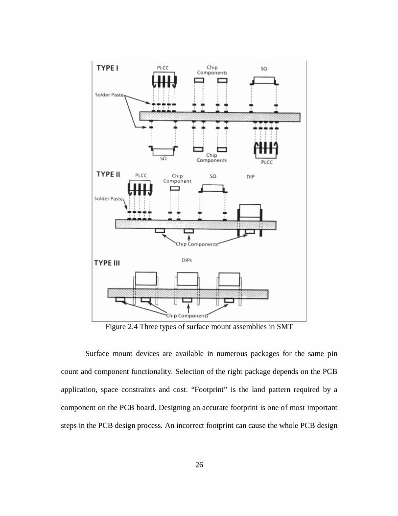
26
Figure 2.4 Three types of surface mount assemblies in SMT
Surface mount devices are available in numerous packages for the same pin
count and component functionality. Selection of the right package depends on the PCB
application, space constraints and cost. “Footprint” is the land pattern required by a
component on the PCB board. Designing an accurate footprint is one of most important
steps in the PCB design process. An incorrect footprint can cause the whole PCB design

27
to fail. Hence it is imperative to have a good understanding of most surface mount
packages and their footprint designs. Frequently used SMT packages are listed below:
1) Resistors and Capacitors: Packages are defined by their dimensions:
0402 (40 mils long and 30 mils wide), 0603, 0805, 1206, 1210, 2010, 2512.
2) MELF (Metal Electrode Leadless Face): used for resistors, jumpers,
ceramic capacitors, tantalum capacitors and diodes. They are cylindrical and have metal
caps for soldering.
3) SOT (Small Outline Transistor): Used for 3 pin devices like transistors,
MOSFETs etc
4) SOIC (Small Outline IC), SOJ (Small Outline J-leaded): They have 50
mil pitch and are generally used for pin count less than 20.
5) PLCC (Plastic Leaded Chip Carrier): These packages also have 50 mil
pitch and are used when the pin count is between 20-84.
6) QFP (Quad Flat Pack): These packages are used when the pin count
exceeds 84 and have a pitch less than 0.5mm.
7) BGA (Ball Grid Array): In contrast to the above packages, BGA has an
array of steel balls underneath the package. They have ball pitches of 40, 50 and 60
mils. This facilitates better trace routing on the PCB. BGA has wide range of pin counts
(16-2400).

28
2.3 High Speed PCB Design
The term “high speed” can be misleading into believing that circuits with high
clock frequency are high speed. It is the rise/fall time of a driving device that
determines whether a circuit design can be termed high speed or not. Figure 2.5 shows
signal integrity effects for a trace driven by two drivers with different rise/fall times.
[16]. Apart from signal integrity, modern PCBs are also required to comply with rules
on EMI/EMC. Selection of number of layers, component placement and trace length are
important parameters in PCB design. A related field known as “signal integrity
analysis” subsumes transmission line effects, crosstalk and power/ground noise. In this
section a theoretical overview of transmission lines effects, EMI/EMC considerations
and use of decoupling capacitors is presented. Looking ahead, few of the output drivers
on TMS320F280X series have a minimum rise/fall time of 2ns. Hence a review of
transmission lines is pertinent to this discussion.
Figure 2.5 Comparison of signal output at load with two drivers
with different rise/fall times

29
2.3.1 Transmission Line Analysis of PCBs
A transmission line may be defined as any pair of conductors that is used to
guide energy in the form of an electromagnetic field from one place to another [18].
Electromagnetic field as the name suggests has two components, an electric and
magnetic field, the two fields being at right angles to each other. The voltage difference
between the transmission line trace and the surrounding planes is a measure of the
strength of the electric field. The magnitude of current flowing in a transmission line is
a measure of the strength of the magnetic field. Hence a PCB can be seen as flow of
electromagnetic fields from point to point. Ensuring that this electromagnetic field does
not exit the board and interfere with external devices is the topic of discussion on EMI.
Electromagnetic waves travel at the speed of light (3x10⁸ m/s). Manipulating the
units, it turns out that an electromagnetic wave travels 12 inches or 30cm of vacuum in
one nanosecond. The distance reduces when traveling in a dielectric medium as in a
PCB. The reduction factor is represented by the following equation
re
cv = (2.1)
where v is the velocity of EM wave in the dielectric medium
c is the velocity of light.
er is the dielectric constant of the insulating medium.
FR-4 which is the commonly used core in PCB has a dielectric constant of 4.1.
Hence using the above expression, the velocity ‘v’ is halved while traveling in a PCB.
This means that an electromagnetic wave requires one nanosecond to travel 6’’ or 15cm
30
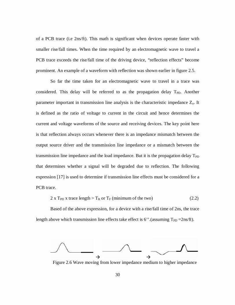
of a PCB trace (i.e 2ns/ft). This math is significant when devices operate faster with
smaller rise/fall times. When the time required by an electromagnetic wave to travel a
PCB trace exceeds the rise/fall time of the driving device, “reflection effects” become
prominent. An example of a waveform with reflection was shown earlier in figure 2.5.
So far the time taken for an electromagnetic wave to travel in a trace was
considered. This delay will be referred to as the propagation delay TPD. Another
parameter important in transmission line analysis is the characteristic impedance Zo. It
is defined as the ratio of voltage to current in the circuit and hence determines the
current and voltage waveforms of the source and receiving devices. The key point here
is that reflection always occurs whenever there is an impedance mismatch between the
output source driver and the transmission line impedance or a mismatch between the
transmission line impedance and the load impedance. But it is the propagation delay TPD
that determines whether a signal will be degraded due to reflection. The following
expression [17] is used to determine if transmission line effects must be considered for a
PCB trace.
2 x TPD x trace length > TR or TF (minimum of the two) (2.2)
Based of the above expression, for a device with a rise/fall time of 2ns, the trace
length above which transmission line effects take effect is 6’’.(assuming TPD =2ns/ft).
Figure 2.6 Wave moving from lower impedance medium to higher impedance

31
Figure 2.7 Wave moving from higher impedance medium to lower impedance
The concept of “reflection” may be explained with the above two figures
(Figure 2.6 and Figure 2.7). When a transverse traveling wave encounters a change in
density of medium (equivalent to change in impedance), it undergoes reflection. The
amount of reflection is determined by the following relation
Reflection % = ol
ol
ZZ
ZZ
+−
100 (2.3)
where Zl is the load impedance or downstream impedance and Zo is the output
or upstream impedance . When the downstream impedance is greater than the upstream
impedance (Zl >Zo), the reflection wave adds to the incident wave. This causes the
overshoot as seen in figure 2.5. From equation (2.3), we notice that ensuring Zl =Zo can
eliminate reflection. This is primarily the principle behind using termination resistors.
Lattice diagram and Bergeron plot are two methods used to analyze reflection in
devices. The former method has been used in this thesis since it is more favorable to
programming. It requires values of the rise and fall times of the driving device, the
output impedance of the source driver, transmission line impedance and input
impedance of the load. Before looking into details of this method, a review on the
different types of transmission lines in a PCB and the lumped approximation of a
transmission line is presented.

32
Microstrip and Stripline are the two kinds of transmission lines used in PCB.
Microstrip consists of a transmission line traveling over a plane with only one plane as a
partner. Stripline has a transmission line along with two planes as partners. Fig 2.8, 2.9,
2.10 and 2.11 illustrates the two types.
Figure 2.8 Surface Microstrip
Figure 2.9 Embedded
Microstrip
Figure 2.10 Stripline
Figure 2.11 Dual Stripline
33
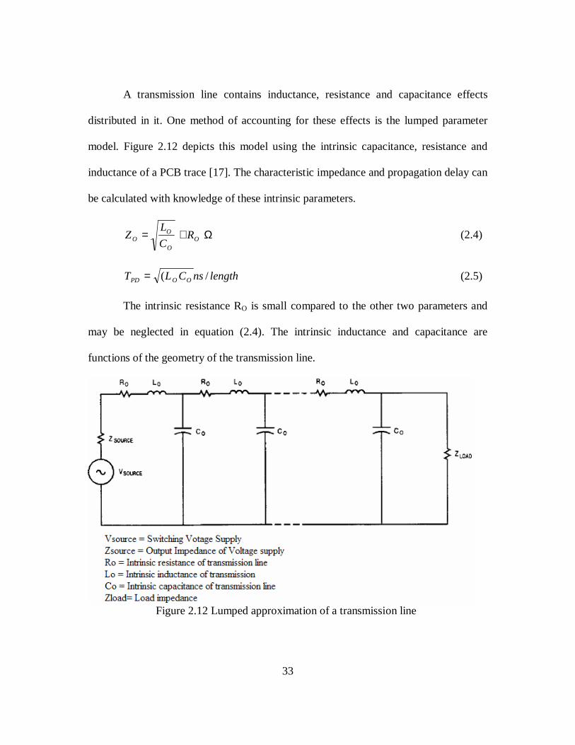
A transmission line contains inductance, resistance and capacitance effects
distributed in it. One method of accounting for these effects is the lumped parameter
model. Figure 2.12 depicts this model using the intrinsic capacitance, resistance and
inductance of a PCB trace [17]. The characteristic impedance and propagation delay can
be calculated with knowledge of these intrinsic parameters.
Ω+= OO
OO R
C
LZ (2.4)
lengthnsCLT OOPD /(= (2.5)
The intrinsic resistance RO is small compared to the other two parameters and
may be neglected in equation (2.4). The intrinsic inductance and capacitance are
functions of the geometry of the transmission line.
Figure 2.12 Lumped approximation of a transmission line
34
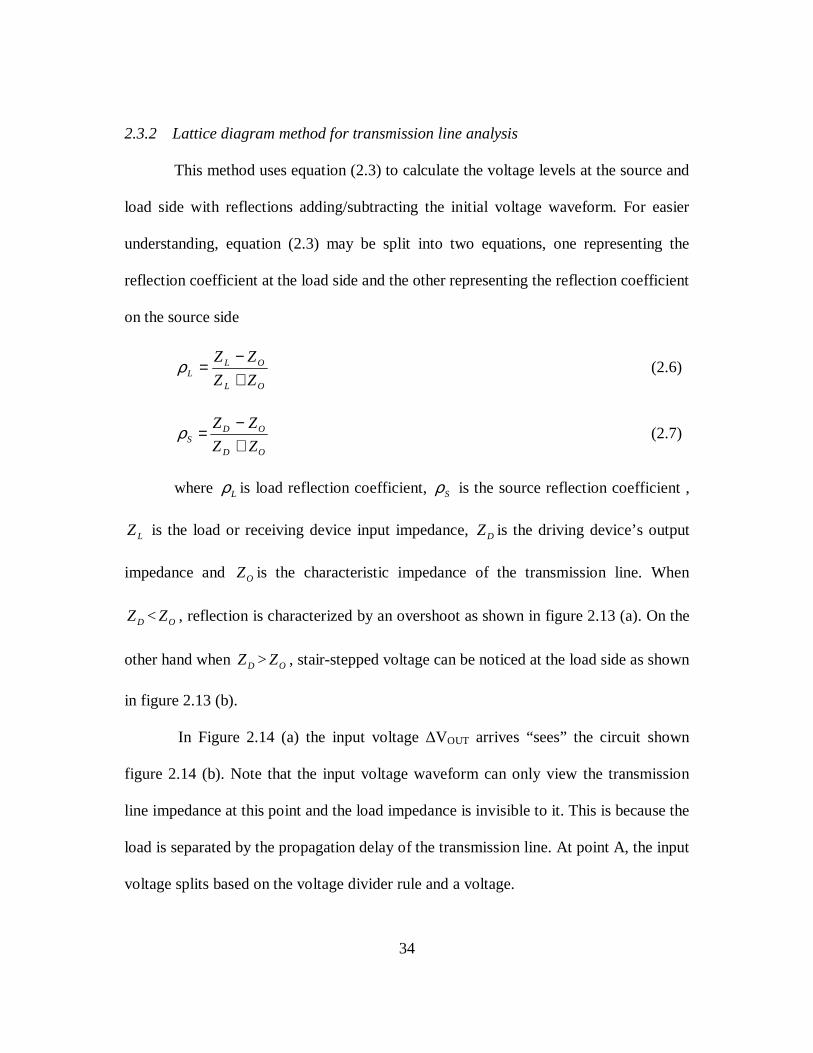
2.3.2 Lattice diagram method for transmission line analysis
This method uses equation (2.3) to calculate the voltage levels at the source and
load side with reflections adding/subtracting the initial voltage waveform. For easier
understanding, equation (2.3) may be split into two equations, one representing the
reflection coefficient at the load side and the other representing the reflection coefficient
on the source side
OL
OLL
ZZ
ZZ
+−
=ρ (2.6)
OD
ODS
ZZ
ZZ
+−
=ρ (2.7)
where Lρ is load reflection coefficient, Sρ is the source reflection coefficient ,
LZ is the load or receiving device input impedance, DZ is the driving device’s output
impedance and OZ is the characteristic impedance of the transmission line. When
DZ < OZ , reflection is characterized by an overshoot as shown in figure 2.13 (a). On the
other hand when DZ > OZ , stair-stepped voltage can be noticed at the load side as shown
in figure 2.13 (b).
In Figure 2.14 (a) the input voltage ∆VOUT arrives “sees” the circuit shown
figure 2.14 (b). Note that the input voltage waveform can only view the transmission
line impedance at this point and the load impedance is invisible to it. This is because the
load is separated by the propagation delay of the transmission line. At point A, the input
voltage splits based on the voltage divider rule and a voltage.

35
Figure 2.13 Transmission line effects
The voltage ∆VO travels down the transmission line. At the end of the
transmission line the voltage waveform ∆VO sees circuit in figure 2.14 (c ). Based on
the value of reflection coefficient Lρ , the reflected wave adds or subtracts from ∆VO.
One of the methods of eliminating reflection is to make Lρ ,=0 by ensuring Zl=ZO. As
will be seen later, this method of termination is known as parallel termination. The
reflected wave now travels down the transmission line and sees the circuit shown in
figure 2.14 (d). The voltage waveform undergoes reflection based on the reflection co-
efficient Sρ . Here again if Sρ can be set to zero, reflection can be avoided. This
method of termination is known as series termination. More on termination will be

36
presented later in this section. Figure 2.15 provides a graphical representation of the
lattice method.[17]
Figure 2.14 Simplified representation of transmission line
Figure 2.15 Analysis of incident and reflected wave
37
An important factor that needs to be considered in transmission line effects, is
the effect of capacitive loading. It alters the propagation delay and characteristic
impedance in the following manner
O
DPDPD C
CTT += 1' ns/length (2.8)
Ω+
=
O
D
OO
C
C
ZZ
1' (2.9)
Note: Lρ and Sρ are the reflection coefficients and VINITIAL is the steady state
voltage prior to switching of the gate. Each TD is a propagation delay (TPD) in duration. A and B represent the driving and receiving ends of the trace respectively.
Figure 2.16 Lattice diagram
38
where CD is the distributed capacitance of the receiving devices. Hence adding a
socket or connecting a single trace to multiple devices can affect the propagation delay
and characteristic impedance. Intuitively, capacitive loading might be considered a
positive outcome since it delays and slows the rise/fall time. But a closer look into the
above equations (2.8) and (2.9) we find that the propagation delay increases where as
the characteristic impedance decreases. Reduction in characteristic impedance results in
ringing or stair stepped response while increased propagation delay only enhances
transmission line effects.
2.3.3 How to avoid reflections?
As mentioned earlier, reflections may be mitigated by manipulating the circuit
such that the reflection coefficient (Lρ or Sρ ) is set to close to zero. This is the basis
for adding terminations to a transmission line. The five commonly used terminations are
1) Series termination resistor
2) Parallel termination resistor
3) Thevenin network
4) RC Network
5) Diode Network
1) Series Termination Resistor: With this solution, a resistor whose value is equal to
DO ZZ −' is placed very close to the driving devices output.(figure 2.17 ) With this series
resistance added, the source voltage ∆VOUT, is halved at point A (figure 2.14 (b)) by the
voltage divider network such that ∆VO=0.5 ∆VOUT. When the voltage waveform ∆VO
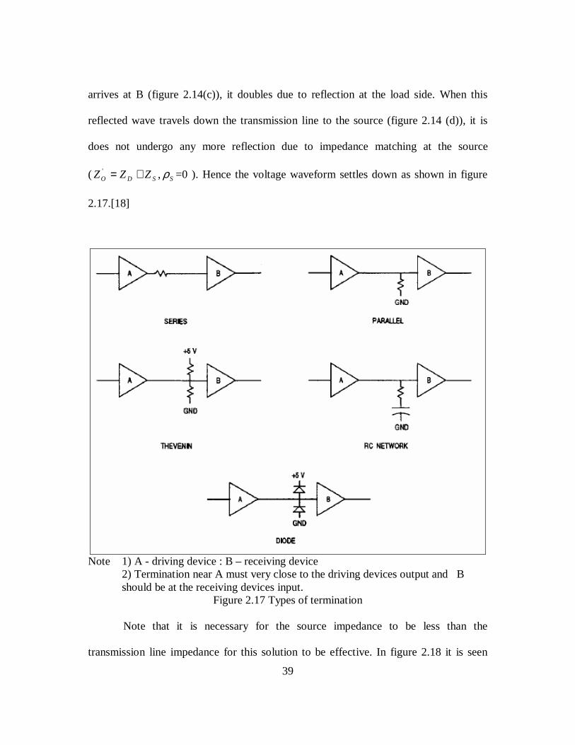
39
arrives at B (figure 2.14(c)), it doubles due to reflection at the load side. When this
reflected wave travels down the transmission line to the source (figure 2.14 (d)), it is
does not undergo any more reflection due to impedance matching at the source
( SDO ZZZ +=' , Sρ =0 ). Hence the voltage waveform settles down as shown in figure
2.17.[18]
Note 1) A - driving device : B – receiving device
2) Termination near A must very close to the driving devices output and B should be at the receiving devices input.
Figure 2.17 Types of termination
Note that it is necessary for the source impedance to be less than the
transmission line impedance for this solution to be effective. In figure 2.18 it is seen

40
that the voltage waveform at the input is stepped being at half the total voltage for a
small duration of time (the propagation delay of the transmission line). During this
period when the voltage waveform is at a voltage level between 0 and logic 1, no valid
information can be transmitted over the line. This reduces the bandwidth of the signal.
For example for a device operating at 50MHz (20ns time period, high for 10ns, low for
10ns), a 2ns propagation delay can reduce the bandwidth by 40% (2xns/10ns =40%).
Hence series termination is not suited for high clock rate devices.
Figure 2.18 Rising and falling edges of 5V CMOS circuit showing effect of
series termination
2) Parallel Termination Resistor: In parallel termination a resistor whose value is equal
to the transmission line impedance is placed at the load side (Zl=ZO). Hence reflection is

41
avoided since Lρ =0. The input voltage waveform remains stable at its initial value.
This implicitly means that the input voltage waveform at point A (figure 2.14 (b)) must
be greater than recognizable logic high voltage for the circuit (VIH). Hence output
impedance of the input driver ZD must be much lesser than the transmission line
impedance ZO. Parallel termination resistor values are generally low (equal to the
transmission line impedance, 100-150 ohms); more current flows through them and
hence more signal power loss.
3) Thevenin Network: As shown in figure 2.19, a Thevenin network can be used to pull
up or pull down a voltage level, such that output voltage waveform does not settle at a
point between logic and logic low [17]. It is particularly used in TTL families which
have an unsymmetrical output. The output impedance when switching from logic high
to low is much lower than when switching from logic low to high. Adding a pull-up can
provide more current to charge up the line, resulting in an improved rising edge. [18].
Figure 2.19 A Thevenin Network used as pullup for a TTL bus

42
4) RC Termination: The objective of this method is to provide termination during when
the edges are “switching” and disconnect it when the logic levels are “steady”. [18].The
resistance is chosen to be equal to ZO, while the capacitor lies in the range 200-600pF.
The RC time constant must be greater than twice the loaded line impedance [17]. The
net result is that the RC time constant effectively slows down the signal while it limits
the overshoot. This methodology is not a recommended for high clock rates, rather
series or parallel termination is preferred [18].
5) Diode Termination: Diodes are generally used to limit the overshoot to
approximately 1V. But they need to be extremely fast, to match the switching frequency
of the driving device [17]. They do not prevent reflections and only helps to reduce
overshoot.
The features of each of the terminations are enumerated in the following table. [17]
Table 2.1 Termination types and their properties
Termination Type
Added Parts
Delay Added
Power Required
Parts Values Comments
Series 1 Yes Low Rs=Zo'-Rd
Good dc noise margin
Parallel 1 Small High R=Zo' Power Consumption is a problem
Thevenin 2 Small High R=2 x Zo' High power for CMOS
RC Network 2 Small Medium R=Zo' C=300pF
Check Bandwidth and added capacitance
Diode 2 Small Low
Limits undershoot: Some ringing at diodes
43
Summarizing, terminations provide a solution for reflection. But the best
engineering practice is to avoid reflection effects by keeping trace length small such
that equation (2.2) is satisfied.
2.3.4 PCB design with EMI/EMC considerations
In the course of this discussion we will find that the techniques used to ensure
signal integrity are closely related to “guidelines” for EMI compliance. It is important to
understand that software and hardware tools that test a PCB for EMI/EMC compliance
is an extensive field and will not be dealt in this thesis.
The cause for Electromagnetic Interference (EMI) can be better understood by
analyzing Gauss Law. It states that
∫∫ = QdAD. (2.10)
where D represents the flux density, dA element of an arbitrary surface and Q is
the total charge enclosed. The flux density is the product of electric field E and the
permittivity of the medium. Gauss Law states that the surface integral of the dot product
of the flux density and the enclosure surface area is equal to the charge enclosed. [19]
This implies that if the total charge enclosed remains constant then so does the
field emanating from the system. This is equivalent to an earth ground which is
characterized by the fact that no matter how much current is put into it, its potential
does not change. For low frequency devices this is easily achievable by connecting the
system ground to the earth ground of the power cable. But for high frequency devices,
this would not work since the inductance of the cable impedes current flow to the earth

44
ground. Hence if it is possible to establish a surface over the system such there is no
variation in potential, there would be no radiation. This is the basis for having a
conductive enclosure over a circuit. The conductive enclosure behaves as a local
ground. But for most systems a conductive enclosure is not viable and is generally
considered a “band aid” solution for a bad PCB design. A good circuit design can
prevent radiations from exiting the system and this is precisely the focus of this
discussion.
As mentioned earlier in this thesis, a PCB circuit can be seen as flow of
electromagnetic energy from point to point. Under certain circumstance, a part of the
energy can amplify and exit the board when flowing through traces with a specific
geometry. Keeping this in mind, we consider two modes of signals that usually flow in
a PCB. They are 1) differential mode and 2) common mode signals. [20].
Differential mode signal is the one that is always considered in circuit analysis.
Current flows from source to a receiver and then returns via ground path to the source.
Since the flow of signal and its return path are opposite, they are known as differential
mode signals.
Figure 2.20 Differential and Common mode currents

45
What is assumed in the above description is that the ground is a perfect
conductor and that return current flows in just one path. But more often due to parasitic
inductance a voltage divider is formed such that majority of the return current flows in
the expected return path (Id) and a small portion in another unintended path (Ic). This
latter current is known as common mode current. This path is unknown and it can
potentially create large “loop areas”. Conventionally differential mode currents are
represented by two currents traveling in opposite directions, while common mode
current is represented by two currents traveling in the same direction as shown in figure
2.21 [20]
Figure 2.21 Conventional representation of differential
and common mode currents
Differential currents if “properly routed” do not cause EMI since the currents
flow in opposite direction; their magnetic fields cancel each other. With respect to
Gauss law, since the currents cancel each other, the net charge Q remains constant and
hence the concept of a local ground is preserved. Common mode currents are

46
detrimental in PCB design since their magnetic fields do not cancel and they create
large loop areas, effectively creating an antenna radiating electromagnetic energy.
Figure 2.22 Basic antenna design
Low frequency currents return via the least resistance path while high frequency
currents return via the least inductance path. [20]. At high frequencies inductance
dominates and presents a higher impedance to the high frequency signal. Hence the
signal tends to return through the least inductance path. Figure 2.23 and 2.24 shows the
return path for low and high frequency currents.
Figure 2.23 At low frequencies current follows path of least resistance
Inductance of single loop coil may be represented by the following equation [19]

47
LI
AxB =)( (2.11)
where B is the magnetic field in the loop, A is the area of the loop and I is the current in
the loop. From this expression, we find that the inductance increases as the loop area A
increases, the inductance L increases. Figure 2.21 shows a simple representation of
antenna.
Figure 2.24 At high frequencies current follows the path of least inductance
Figure 2.25 Distribution of high frequency current density underneath a signal trace

48
Traces in a PCB can behave as antennas if they form significantly large “loop
areas”. Larger loop areas increases the inductance and hence the gain of the antenna that
emits electromagnetic radiation. Moreover as shown in figure 2.25 [21], high frequency
currents follow a return path right below the signal, which is the path of least
inductance. If there are obstructions or slots in the ground plane, the return current will
have to take a longer path, resulting in a larger loop area. This is shown in figure 2.26.
Note that this geometry represents the well known “slot antenna”.
Figure 2.26 Routing a trace over a slot in a plane
can cause large loop area
Summarizing, EMI can be reduced with the following:
1) High frequency traces must be kept as short as possible (example clock
signals),
2) Signal traces must be close to a ground plane, to reduce loop area of the
signal. Ensuring that only differential signals exists, automatically minimizes or
eliminates common mode signals. Best EMI reduction can be achieved by having every
signal layer associated with a ground layer beneath it.

49
3) The ground plane must be solid without too many discontinuities due to
vias.
4) All sources of parasitic inductance must be minimized. (example
sockets, leads of components etc).
The other factors key to a good PCB design are listed below
1) Board layer selection
2) Component placement
3) Decoupling capacitor
2.3.4.1 Board Layer Selection:
Selection of the number of layers for a PCB depends on a number of factors like
a) Complexity of schematic: The number of nets or connections in the circuit
and the number of components.
b) Type of components: Surface mount devices, especially fine pitch devices
have high density of pins and hence it becomes nearly impossible to route them on a 2
layer board.
c) Trace width: If the circuit requires high currents, trace widths must be wider,
hence occupying more space on the board.
d) Real estate constraint: This is generally considered the prime motive for layer
selection. It is possible to reduce the size of the board by increasing the number of
layers. But higher number of layers cost more. At times to reduce cost, one might
consider reducing the number of layers and increase the board size. This might not be

50
prudent for high speed designs that have constraints on trace length. More number of
layers provides the extra degree of freedom in routing, allowing components to be place
closer and hence shorter trace lengths. Figure 2.27 shows trace length comparison
between a 4 and 6 layer PCB.
Figure 2.27 Comparison of trace length with number of layers in a PCB
e) Cost: Since higher number of layers provides extra latitude in routing and
also better EMI suppression, one might be tempted to be use it more frequently. But
they cost much more than boards with lesser layers and hence must be considered in the
design stage.
Figure 2.28 and 2.29 [22] depicts the commonly used PCB layer stack up.

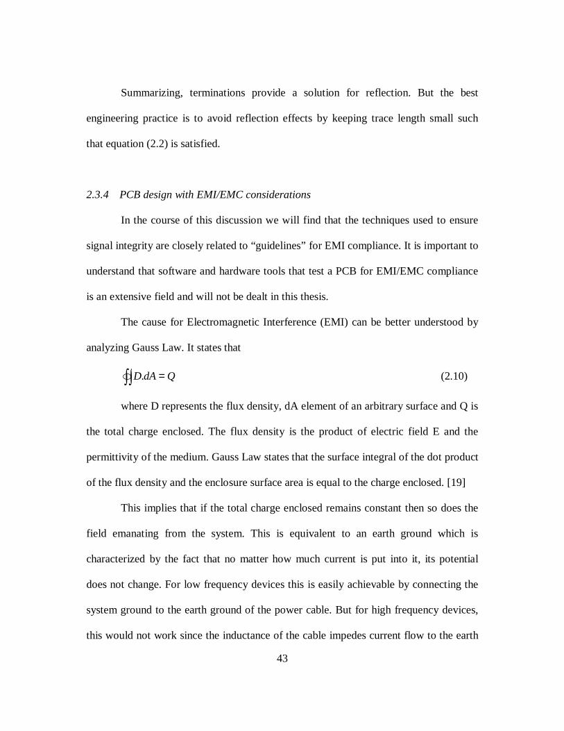
51
Figure 2.28 PCB layer stackup 1
52
Figure 2.29 PCB layer stackup 2
2.3.4.2 Component Placement:
Optimal placement of components is one of the most important steps in PCB
design. In the section on EMI considerations, emphasis was placed on having small
loop currents. This can be achieved by placing functionally related components
together. When placing components the length of traces must be estimated in high speed
design. If the traces exceed the maximum permissible length to prevent transmission
line effects, then termination resistor values must be calculated and updated in the
schematic.
If the circuit has analog and digital circuitry, it is necessary to functionally
separate the two modules. A separate analog and digital ground is not necessary. [23].
Since the return signal generally follows the path beneath the trace, the analog and
digital sections are partitioned such that none of the signals cross each other. Hence

53
good routing discipline can prevent contamination of analog and digital signals with a
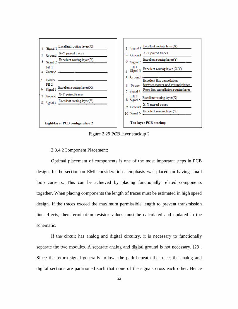
single ground plane. Figure 2.31 shows the comparison between split and single ground
planes [23]
Figure 2.30 Functional distribution of the custom DSP board
2.3.4.3 Bypass Capacitor Selection and Placement
The term “bypass” may be defined as “a means of circumvention or to avoid (an
obstacle) by using an alternative channel, passage or route”. [24]. While the term
“decouple” may be defined as “to reduce or eliminate the coupling of (one circuit part
from another)”. A capacitor plays the above two roles in PCB design.
Definition of a bypass capacitor – A bypass capacitor stores an electrical
charge that is released to the power line whenever transient voltage spike occurs. It
provides a low-impedance supply, thereby minimizing the noise generated by the
switching outputs of the device. [25].
54
Figure 2.31 Trace and ground current on split and single ground planes
A decoupling capacitor is defined as one that “removes RF energy generated on
the power planes by high frequency components. Decoupling capacitors also provide a
localized source of dc power for devices or components, and are particularly useful in
reducing peak current surges propagated across the board”[25].
In short bypass/decoupling capacitors 1) reduce high frequency components in
the signal due to fast switching logic by shunting them to ground.

55
2) Prevents fluctuation of the power (Vcc) pin by acting as a low impedance
voltage source.
Since the same capacitor can provide both the above features, the term bypass
and decoupling has been used interchangeably. For this discussion the term decoupling
capacitor will be used.
2.3.4.4 High frequency behavior of Decoupling Capacitor
The equivalent circuit of a decoupling capacitor is illustrated in figure 2.32 [18]
Figure 2.32 Equivalent circuit of decoupling
capacitor
The effective impedance of the above circuit is given by the expression
22 )( CLs XXRZ −+= (2.12)
where Rs is the Equivalent Series Resistance (ESR)
XL is the impedance of Equivalent Series Inductance (ESL) = 2πfL
Xc is impedance of the capacitor C = 1/2πfC
For this series equivalent circuit, the impedance keeps decreasing from DC (0
Hz) till the series resonant frequency when XL =Xc. At this frequency the impedance

56
offered by the capacitor is the least and is equal to Rs. Figure 2.33 illustrates this
behavior.
Figure 2.33 0603 ceramic capacitor impedance vs frequency (C=1uF, ESR=12mΩ,
ERL=2nH)
Hence as seen in figure 2.33, above the self resonant frequency, the inductive
behavior of the decoupling capacitor dominates and prevents shunting of high
frequency noise.
High speed logic families like “ACT or F” have fast rising edges (0.8-2ns) and
hence have higher RF spectrum [C11]. Figure 2.34 provides a comparison of series
resonant frequencies of different valued capacitors and their spectrum range. The leads
of a capacitor are the major contributor to the inductance. Higher inductance reduces the
series resonant frequency. Axial and radial capacitors have significantly large lead
inductances. Hence surface mount capacitors are recommended for high speed

57
applications. Table 2.2 provides a comparison of series resonant frequencies of thru
hole mount and surface mount capacitors.
Figure 2.34 Self-resonant frequencies of capacitors vs logic families with 0.25’ leads
Table 2.2 Comparison of Series Resonant Frequency of Thru Hole and Surface Mount capacitors [22] [18]
Axial 0.25' leads (Thru Hole Mount)
0603 Ceramic (Surface Mount)
Capacitor Fres(MHz) ESL Fres(MHz) ESL 1uF 2.5 15nh/inch 6 0.7nH
0.1uF 5 15nh/inch 18 0.6nH 0.01uF 15 15nh/inch 50 0.5nH

58
The power and ground planes of the PCB behave as a large parallel plate
capacitor with capacitance given by the relation [22]
d
AC rεε 0= (2.13)
where ε0 is the dielectric constant of free space = 8.854x10⁻¹² F/m.
εr is the relative dielectric constant = 4 for FR4 core material commonly used in
PCBs
A is the area of the power planes in square meters
d is the distance between the power and ground planes in meters
For a distance of 0.01 inches, the power and ground planes will have a
capacitance of 100pF/in2. Decoupling capacitors can form a parallel resonant circuit
with the PCB capacitance. For a parallel resonant circuit, the impedance offered tends
to a very high value and is restricted only by the series equivalent resistance of the
capacitor.
Figure 2.35 Equivalent circuit of decoupling capacitor with the equivalent PCB capacitance

59
At parallel resonance the magnitude of impedance offered by the parallel circuit
is indirectly proportional to the ESR of the capacitor and is given by the following
expression [18]
pcbxCESR
ESLZ
.= (2.14)
Hence it is desirable to have ESR in the range sufficiently low to be an effective
capacitor at low frequencies and sufficiently high to control the impedance spike at the
parallel resonance frequency [18].
Figure 2.36 Impedance at parallel resonance versus ESR (1uF 0603 ceramic)
2.3.4.5 Selection of decoupling capacitor
The following procedure may be followed to select decoupling capacitors [22]
Determine the maximum current draw anticipated on the board. Assume all gates switch

60
at the same time. Include the effect of power surges by logic crossover (cross
conduction currents)
1) Calculate the maximum amount of power supply noise permitted by the
logic devices used. Factor in a safety margin.
2) Determine the maximum common-path impedance tolerable. This is
determined by
I
VX
∆∆=max (2.15)
3) If solid planes are used, Xmax is allocated to the connection between
power and ground.
4) Calculate the inductance of the interconnect cabling from the power
supply to the board. Add this value to Xmax to determine the frequency below which the
power supply wiring is adequate. If all gates switch simulataneously, power supply
noise will be less than ∆V.
pswpsw L
XF
π2max= (2.16)
5) Below frequency Fpsw, the power supply wiring is fine. Above Fpsw, bulk
capacitors are required. Calculate the value of capacitor that has an impedance Xmax at
frequency Fpsw.
max2
1
XFC
pswbypass π
= (2.17)

61
Since one of the reasons for using decoupling capacitors is to provide a low
impedance supply to the voltage pins of the chip, it is imperative to place them as close
as possible to the IC pins. As mentioned earlier, inductance increases with loop area. By
placing the decoupling capacitors closer to the IC, a smaller loop is formed; a lower
inductance and lesser impedance to current. Figure 2.37[25] shows that the power line
disturbance increases as the decoupling capacitor distance is increased.
Figure 2.37 Test performed on TI ABT541, Vcc line disturbance versus capacitor size at different distances
62
2.3.5 Introduction to OrCAD Capture and Layout
OrCAD Capture and OrCAD Layout are PCB design softwares from Cadence
Design Systems. This software has been used in this thesis for designing the PCB.
OrCAD Capture is a software that helps in preparing schematics while OrCAD layout
helps in component placement and routing of the connections. The following steps
provide a broad overview in designing a PCB using OrCAD Capture and Layout. Figure
2.38 depicts a snapshot of OrCAD Capture.
OrCAD Capture:
1) Draw the schematic using OrCAD Capture.
2) Associate each component in the circuit with a footprint. (Most frequently
used footprints for packages like DIP, SOT are available in the OrCAD library. New
footprints can be created in OrCAD Layout)
3) Generate a netlist file (file containing all description of the circuit).
OrCAD Layout:
4) Import netlist to OrCAD Layout, specify number of layers for the PCB.
5) Draw PCB board and place components. The Design Rule Check (DRC)
option can be used to check if the design meets the standards set for PCB design. (like
minimum component spacing, via spacing etc)
6) Use a combination of manual and auto routing to route all the nets
(connections between components are known as nets). OrCAD Specctra has the auto
routing feature integrated with OrCAD Layout.

63
7) Verify whether the routed board meets all the design guidelines using the
DRC option
8) Generate gerber files. Gerber files is the standard industry format accepted
by PCB fabricators. It contains details of all the board layers and dimension of drill
holes.
Figure 2.38 Schematic view of a circuit in OrCAD Capture

64
CHAPTER 3
THREE PHASE INVERTER
An inverter is used to convert DC signal to AC. AC Motor drives typically
require 3 phase AC signals at the stator for their operation. The ability to control voltage
and frequency of AC signals allows flexibility in improving the efficiency of AC
motors. In this chapter an overview of the working of a three phase inverter is presented
followed by techniques to produce modulating signals to control the inverter. Space
Vector Modulation (SVM) and Sinusoidal Pulse Width Modulation (SPWM) are the
popular PWM techniques in use to produce modulating control signals. Specifically
SVM is analyzed and tested on a 3 phase inverter using the custom DSP board
developed in this thesis. Over the years SVM has gained importance due to its inherent
ability to increase the linear modulation range as well as improved Total Harmonic
Distortion. [26]. At the same time research has shown that regular sampled sinusoidal
modulation too can provide the same if not better performance than SVM. [27][28]. A
comparison of these two techniques is presented in this chapter.
3.1 Three Phase Inverter - Working
Figure 3.1 shows a three phase inverter connected to a balanced three
phase load. Switches Sa, Sb, Sc, Sa’, Sb’ and Sc’ are assumed to work ideally; i.e. when
the switch is closed maximum current flows and there is zero voltage drop across the

65
switch, while when it is open, zero current flows and maximum voltage drop across the
switch. Hence under ideal conditions there would be zero power loss in the switch. But
practically switches have a small leakage current flowing through them in the OFF
state, and a small voltage drop in the ON state (conduction losses). Moreover the
transition from OFF to ON and vice-a-versa is not a perfect step function. Hence there
would be losses during change of states (switching losses). But overall inverter
efficiencies upto 95% [29] can be achieved in this mode of operation rather than
operating the switch in its linear I-V region. The diodes across the switches are used to
allow reverse inductive motor current to flow in the inverter, since switches
(MOSFETs, IGBTs) allow current only in one direction. To prevent short-circuit, both
the upper and lower switches are never turned ON together. The turn ON and turn OFF
times of switches are usually not identical and hence it is necessary to place a deadband
between the turn ON and turn OFF periods.
Figure 3.1 Three phase inverter with balanced load

66
Figure 3.2 Switching states of a three phase inverter

67
With the three upper switches there are 23=8 possible switching states.
These switching states are represented in figure 3.2. For two of the switching states (000
and 111), the voltage produced across each of the phases is zero. Though these states
produce “null voltage”, they play an important role in increasing the linear modulation
range as well as reduction in Total Harmonic Distortion (THD).
Consider the case when switch Sa=1, Sb=0, Sc=0. The equivalent circuit is
shown in figure 3.3
Figure 3.3 Equivalent circuit with switch sequence (100)
dcaganng
dcdcdcbnanab
dcdc
cnbn
dcdc
an
dcdc
VVVHenceVsystembalancedaFor
VVVVVV
VZ
Vx
ZVV
VxZZ
VIZV
Z
V
Z
VI
3
2.0
3
1
3
23
1
3
2
2
3
2
3
2
3
2
2
3
===
=
−−=−=
−=−==
===
==
(3.1)

68
Using a similar approach the line-neutral and line-line voltages can be
calculated for the remaining switching sequences and is shown in table 3.1. From the
table we notice that the line to line voltages varies between +Vdc and –Vdc. This is the
maximum attainable voltage given a DC bus voltage of Vdc. [30].
Table 3.1 Switching patterns in a 3 phase inverter Switching
Pattern Line to neutral
voltages Line to Line
Voltages Voltage V Sa Sb Sc Van Vbn Vcn Vab Vbc Vca V0 0 0 0 0 0 0 0 0 0 V1 1 0 0 (2/3) (-1/3) (-1/3) 1 0 -1 V2 1 1 0 (1/3) (1/3) (-2/3) 0 1 -1 V3 0 1 0 (-1/3) (2/3) (-1/3) -1 1 0 V4 0 1 1 (-2/3) (1/3) (1/3) -1 0 1 V5 0 0 1 (-1/3) (-1/3) (2/3) 0 -1 1 V6 1 0 1 (1/3) (-2/3) (1/3) 1 -1 0 V7 1 1 1 0 0 0 0 0 0
3.2 Pulse Width Modulation (PWM)
PWM is a modulation strategy wherein the amplitude of a low frequency signal
is represented as the duty cycle of a fixed high frequency carrier signal. Figure 3.7
shows a low frequency sinusoid represented on a PWM signal. The aim is to create a
train of switched pulses which have the same fundamental volt-second average as a
target waveform at any instant of time. The secondary objective is determine the most
effective way of arranging the switching processes to minimize unwanted harmonic
distortion and switching losses. [34].
The two popular alternatives to determine the switch ON times in a PWM are

69
1) Naturally sampled PWM: Switching occurs at the intersection of a target
reference waveform and a high frequency carrier.
2) Regular or Uniformly sampled PWM: Switching occurs at the intersection
between a regularly sampled reference waveform and a high frequency carrier. These
two switching strategies are shown in figure 3.4.
All fixed frequency open loop PWM strategies can be explained in terms of
1) Switched pulse width determination.
2) Switched pulse position within a carrier interval
3) Switched pulse sequence within and across carrier intervals.
The harmonic performance of a specific PWM implementation then results from the
effects of the above three factors and the following.
1) The harmonics generated by the phase leg switched waveform.
2) Harmonic cancellation that may occur between individual phase leg
switched outputs. [34].
The above factors will be considered when comparing Space Vector and
Sinusoidal PWM techniques.
3.3 Space Vector Pulse Width Modulation (SVPWM)
The three phase voltages (Van,Vbn, and Vcn) may be represented by a single
space vector Vref given by the following expression [31]
3
4
3
20 )()()()(
ππj
cn
j
bnj
anref etVetVetVtV>−>−>−>−
++= (3.2)
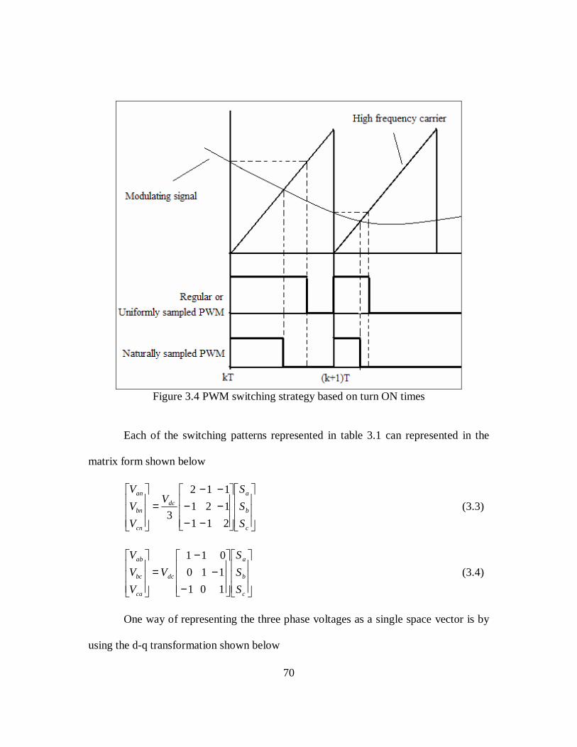
70
Figure 3.4 PWM switching strategy based on turn ON times
Each of the switching patterns represented in table 3.1 can represented in the
matrix form shown below
−−−−−−
=
c
b
a
dc
cn
bn
an
S
S
SV
V
V
V
211
121
112
3 (3.3)
−−
−=
c
b
a
dc
ca
bc
ab
S
S
S
V
V
V
V
101
110
011
(3.4)
One way of representing the three phase voltages as a single space vector is by
using the d-q transformation shown below

71
−
−−
=
=
2
3
2
30
2
1
2
11
3
2s
abcsdq
K
where
fKf
(3.5)
The d-q transformation is equivalent to projection of the three phase vectors on
the orthonormal d-q axis.
Figure 3.5 Representation of 3 phase signals in dq refrence frame
bnbn
cnbnq
cnbnan
cnbnand
VcV
VVV
VVV
VVVV
23
230
)30cos()30cos(0
5.05.0
)60cos()60cos(
+−=
+−=−−=
−−=
(3.6)

72
−
−−=
cn
bn
an
q
d
V
V
V
V
V
23
230
21
211
3
2 (3.7)
22qdref VVV +=
For each of the switching patterns in table 3.1, a corresponding d-q voltage
vector can be calculated. For example for the first non zero switching sequence (100) in
table 3.1, Vd and Vq may be calculated using equation 3.7
−
−
−
−−=
313
13
2
23
230
21
211
3
2
q
d
V
V
32
03
2
=
=
=
dq
q
d
V
V
V
The same is repeated for the rest of the switching patterns and is shown in table 3.2
Table 3.2 Switching pattern with Vd , Vq and Vdq voltages Switching
Pattern Line to neutral
voltages Vd, Vq and Vdq Voltage V Sa Sb Sc Van Vbn Vcn Vd Vq Vdq V0 0 0 0 0 0 0 0 0 0 V1 1 0 0 (2/3) (-1/3) (-1/3) (2/3) 0 (2/3) V2 1 1 0 (1/3) (1/3) (-2/3) (1/3) (-1/√3) (2/3) V3 0 1 0 (-1/3) (2/3) (-1/3) (-1/3) (-1/√3) (2/3) V4 0 1 1 (-2/3) (1/3) (1/3) (-2/3) 0 (2/3) V5 0 0 1 (-1/3) (-1/3) (2/3) (-1/3) (1/√3) (2/3) V6 1 0 1 (1/3) (-2/3) (1/3) (1/3) (1/√3) (2/3) V7 1 1 1 0 0 0 0 0 0

73
Each of the voltage vectors corresponding to the 8 switching states is shown in
figure 3.6 [32]. Note the presence of the zero vectors at the origin (V0 and V7). They
play an important role in the switching pattern and are primarily responsible for third
harmonic injection.
Figure 3.6 Switching patterns of space vectors
The required output voltage vector is represented by the reference vector Vref.
For example, if the required output line to line voltage is given by the following
equations
)120cos(
)120cos(
)cos(
+=−=
=
ααα
VV
VV
VV
ca
bc
ab
(3.8)

74
, then Vref = V/√3. This is because line to neutral voltages was used in the d-q
transformation.
‘α’ = 2πft; where ‘f’ is the fundamental frequency of the modulating signal.
The objective of space vector PWM technique is to approximate the reference
voltage vector Vref, by a combination of the eight switching patterns [33]. In a small
period Tz (the period of the PWM signal), the average output voltage of the inverter is
assumed to be same as Vref in the same period. The reference output Vref is
approximated using the adjacent voltage vectors in each sector.
∫∫∫∫+
+
++=ZZ T
TT
TT
T
TT
ref VVVV21
21
1
1
02
0
1
0
(3.9)
Using d-q axis
( )( )
+
+
+
=
3)1(sin
3)1(cos
3
2
3sin
3cos
3
2
)sin(
)cos(21 π
π
π
π
αα
n
n
VTn
nVTVT dcdcrefz (3.10)
where ‘n’ is the sector number =0,1..5
Simplifying the above equation, T1 and T2, can be represented by the following
set of equations for any sector
)(
3
)1(sin
3
3sin
3
210
2
1
TTTT
n
V
VTT
n
V
VTT
Z
dc
refZ
dc
refZ
+−=
−−=
−=
πα
απ
(3.11)

75
Hence in sector 0, voltage vector V0 (Sa=1,Sb=0,Sc=0) is applied for T1 units
of time and V1 (Sa=1,Sb=1,Sc=0) for T2 units of time. This effectively means that in
sector 0
a) Sa is turned ON for T1+T2 units of time.
b) Sb is turned ON for T2 units of time.
c) Sc is turned OFF.
T0 represents the null pulse time (voltage vectors V0 and V7). In order to
ensure minimum switching frequency of each inverter leg, it is necessary to arrange the
switching sequence in such a way that the transition from one state to the other is
performed by switching only one inverter leg [26]. This done by distributing the null
state among V0(000) and V7(111) such that each voltage vector equals T0/2.
One PWM (symmetrical) switching period in sector 0 is shown in figure 3.7. Table 3.3
shows the time instants for all the sectors
Figure 3.7 Switching time instants of Sa,Sb and Sc
In this thesis, Space Vector PWM signals are generated using the DSP board
and tested on a 3 phase inverter.

76
Table 3.3 Switching time instants for each sector
Sector Switch Upper
Switches Lower Switches S1 T1+T2+T0/2 T0/2 S3 T2+T0/2 T1+T0/2
0 S5 T0/2 T1+T2+T0/2 S1 T1+T0/2 T2+T0/2 S3 T1+T2+T0/2 T0/2
1 S5 T0/2 T1+T2+T0/2 S1 T0/2 T1+T2+T0/2 S3 T1+T2+T0/2 T0/2
2 S5 T2+T0/2 T1+T0/2 S1 T0/2 T1+T2+T0/2 S3 T1+T0/2 T2+T0/2
3 S5 T1+T2+T0/2 T0/2 S1 T2+T0/2 T1+T0/2 S3 T0/2 T1+T2+T0/2
4 S5 T1+T2+T0/2 T0/2 S1 T1+T2+T0/2 T0/2 S3 T0/2 T1+T2+T0/2
5 S5 T1+T0/2 T2+T0/2
3.4 Sinusoidal modulation and third harmonic injection
Consider the following line to neutral sinusoidal modulating signals
Va=Vsin(ωt) (3.12)
Vb=Vsin(ωt-120) (3.13)
Vc=Vsin(ωt+120) (3.14)
Pulse Width Modulation of the switches of the inverter produces output voltages
between 0 and Vdc. Figure 3.7 represents a sine wave imposed on a PWM signal. The
peak value of the sine wave that can be produced equals Vdc/2.
i.e. V=Vdc/2.

77
Figure 3.8 Sinusoidal Pulse Width Modulated Signal
With the line to neutral voltages represented by equation 3.12, 3.13 and
3.14, the peak line to line voltage that can be produced equal √3V=√3Vdc/2 =
0.866Vdc. Hence the peak possible voltage (Vdc) cannot be achieved using simple
sinusoidal modulation. Figure 3.9 shows this condition. For ease of analyzing only Va,
Vb and Vab are considered. The same results may be applied to Vbc and Vca.
From equations (3.12) and (3.13)
Vab = Va-Vb
= Vsin(ωt)-Vsin(ωt-120) (3.15)
The maximum value occurs when dVab/dt=0
dVab/dt = Vcos(ωt)+Vcos(ωt-120) (3.16)
Vcos(ωt)=-Vcos(ωt-120)
ωt=60o satisfies the above condition.
Hence a signal that peaks at Va=Vsin(60)=0.866V can produce maximum Vab.
From figure 3.9, we find that when Vab reaches its maximum value of √3V, Va and Vb
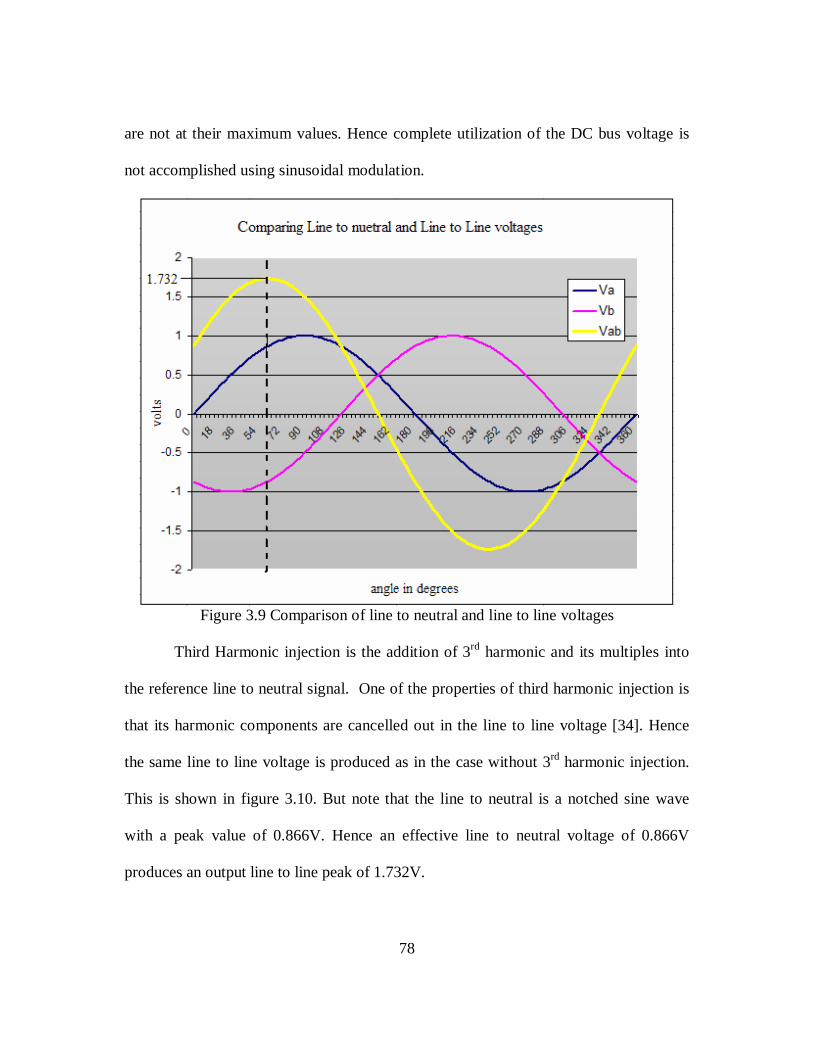
78
are not at their maximum values. Hence complete utilization of the DC bus voltage is
not accomplished using sinusoidal modulation.
Figure 3.9 Comparison of line to neutral and line to line voltages
Third Harmonic injection is the addition of 3rd harmonic and its multiples into
the reference line to neutral signal. One of the properties of third harmonic injection is
that its harmonic components are cancelled out in the line to line voltage [34]. Hence
the same line to line voltage is produced as in the case without 3rd harmonic injection.
This is shown in figure 3.10. But note that the line to neutral is a notched sine wave
with a peak value of 0.866V. Hence an effective line to neutral voltage of 0.866V
produces an output line to line peak of 1.732V.
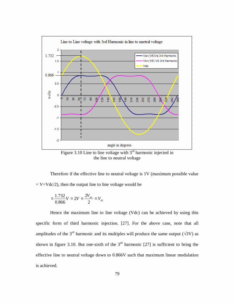
79
Figure 3.10 Line to line voltage with 3rd harmonic injected in
the line to neutral voltage
Therefore if the effective line to neutral voltage is 1V (maximum possible value
= V=Vdc/2), then the output line to line voltage would be
dcdc V
VVV ====
2
22
866.0
732.1
Hence the maximum line to line voltage (Vdc) can be achieved by using this
specific form of third harmonic injection. [27]. For the above case, note that all
amplitudes of the 3rd harmonic and its multiples will produce the same output (√3V) as
shown in figure 3.10. But one-sixth of the 3rd harmonic [27] is sufficient to bring the
effective line to neutral voltage down to 0.866V such that maximum linear modulation
is achieved.
80
For sinusoidal modulation, the modulation index m is defined as
1==V
Vm
For sinusoidal modulation with 3rd harmonic injection, modulation index
m is equal to
15.13
2
866.0===
V
Vm
3.5 Comparison of Space Vector and Sinusoidal PWM techniques
Space Vector PWM (SVM) as seen above can produce the maximum possible
line to line voltage by increasing the linear modulation range (2/√3 or 1.15 times ). This
is accomplished due to third harmonic injection “inherent” in SVM. Comparisons with
respect to SPWM has shown that SVM is much better due to higher linear modulation
range and lower baseband distortion [27]. Figure 3.11 shows three kinds of modulating
phase signals sinusoidal modulation (Va), sinusoidal modulation + (1/6)th 3rd harmonic
(Va+3rd harmonic) and space vector modulated signal (Va_SVM).
From figure 3.11 we find that due to the similarity of the signals, it would be
appropriate to compare SV signals with sinusoidal modulated signals + 3rd harmonic
injection. In SVM, the switching times were calculated and assigned to a specific type
of PWM representation. Hence SVM can also be regarded as form of carrier based
PWM technique with a low frequency modulating signal on a high frequency carrier
signal. With this perspective, comparison of the different modulating techniques can be
distinguished between the form of the modulating signal and the carrier PWM.

81
Comparison of modulating signals
-1.5
-1
-0.5
0
0.5
1
1.5
0 18 36 54 72 90 108
126
144
162
180
198
216
234
252
270
288
306
324
342
360
angle in degrees
volts
Va
Va+3rd harmonic
Va_SVM
Figure 3.11 Comparison of phase modulating signals
The following features will be considered in comparing all the possible
modulating signals.
1) Linear modulation range extension to the maximum value of 1.15.
2) Total Harmonic Distortion
The relationship between SVM and asymmetrical regular sampled PWM was
established by considering a sector based 3rd harmonic injected sinusoid [28]. This was
done in order to maintain equal null pulse times (t0 and t7) in the pulse pattern. The
addition of equal null sequence (t0 and t7), increased the linear modulation range to
(2/√3). The modulating signals were represented by the following expressions.

82
)]3sin(3
4[sin)(
)]3sin(3
2[sin)(
)]3sin()[sin()(
kkkc
kkkb
kkkA
TxTTF
TxTTF
TxTTF
+
−=
+
−=
+=
π
π (3.17)
where ‘x’ is given by
==
∈+−
∈−−
−∈
=
5...1,0;3
;6
1
6
11,
2
3,
6
5,
2;
)3sin(2
)3
sin(
2
3,
6
7,
2,
6;
)3sin(2
)3
sin(
6
7,
6
5,
6,
6;
)3sin(2
)sin(
jj
T
TT
T
TT
T
TT
T
x
k
kk
k
kk
k
kk
k
π
πππππ
πππππ
ππππ
(3.18)
This signal generated an identical phase modulating phase signal as SVM
shown in figure 3.11. This expression established the time domain relationship between
space vector modulated and regularly sampled sinusoidal modulation signals. Being
sector dependent, it offered no advantage over SVM in computational complexity.
Considering double sided uniform sampled PWM (UPWM), the switching
patterns was established to be identical to SVM [27]. Addition of 3rd harmonic to the
sinusoidal UPWM, only increases the linear modulation range and does not cause base
band distortion. This shows that SVM signals are quite similar to uniformly sampled
SPWM signals with 3rd harmonic injection. But an important difference is that SVM
signals have equal null pulse times (t0=t7), while SPWM have unequal null pulse times.

83
Research has shown that (1/6th) 3rd harmonic has higher THD in comparison with equal
null pulse (t0-t7) (equivalently SVM signal) modulating signal. This is shown in figure
3.12 [28]
Figure 3.12 THD for four PWM strategies
In figure 3.11, analysis was performed on asymmetric regular sampled PWM
signals. One fourth 3rd harmonic injection as shown in figure 3.12, is known to have
lower THD compared to other modulation schemes. But this is at the cost of a slightly
lower linear modulation range (1.12) [34].
Asymmetric naturally sampled PWM signals are known to have better THD
than other PWM modulation strategies [31]. But such signals are usually difficult to
implement in a DSP. In this thesis symmetrical regular sampled modulation signals will
be simulated in MATLAB SIMULINK to compare the following modulation schemes

84
1) Space vector PWM
2) Sinusoidal with (1/6)th 3rd harmonic injection PWM.
3) Sinusoidal PWM.

85
CHAPTER 4
RESULTS
4.1 High Speed Printed Circuit Board Design
Based on the concepts presented in Chapter 2, a custom DSP board was
successfully developed and tested to drive a 3 phase inverter. The PCB design process
is shown in figure 4.1
4.1.1 Creation of schematic
The DSP board was designed to fully utilize the features of the TMS320F2808
DSP. They include the following
1. General Purpose IO Interface
2. Interface for analog inputs. The number of analog inputs was extended using
a multiplexer configurable using one of the GPIO pins.
3. EEPROM (256K) and Real Time Clock support using I2C.
4. CAN Interface
5. RS-232 Interface
6. 14-pin JTAG
The schematics were prepared using OrCAD Capture with [35] as reference.
4.1.2 Component Selection, design of footprints
All the components selected were Surface Mount. As mentioned in chapter 2,
this was done to reduce EMI, reduce space and satisfy trace length constraints. The

86
footprint for commonly used components like 0805 resistor is available in OrCAD
Layout. For the rest, footprints were designed in Layout based on mechanical
information provided in their respective datasheets.
As an industry standard, list of components numbers, their manufacturers and
footprints are specified in a text file known Bill of Materials (BOM). This file is
available in Appendix B.
Figure 4.1 Flowchart of PCB design process
Create schematic
Select components, design footprints, generate net list
and prepare Bill of Materials (BOM)
Decide on number of layers, size of board
A
Design component placement on board
Identify high speed nets, perform transmission line
analysis.
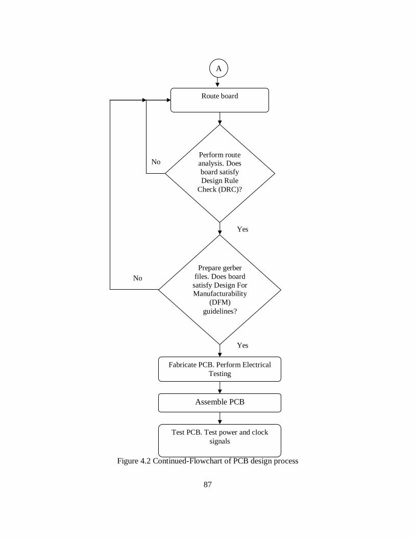
87
Figure 4.2 Continued-Flowchart of PCB design process
Route board
Perform route analysis. Does board satisfy Design Rule
Check (DRC)?
Prepare gerber files. Does board satisfy Design For Manufacturability
(DFM) guidelines?
Fabricate PCB. Perform Electrical Testing
Assemble PCB
Test PCB. Test power and clock signals
Yes
No
No
Yes
A

88
Figure 4.3 Functional distribution of the DSP board
4.1.3 Component Placement
This is one of most important steps in the PCB design process. The board was
divided into functional areas as shown in figure 4.3. This step is revisited each time
routing rules/design constraints fail.
4.1.4 Number of layers and size of board
The custom DSP board was designed to have a dimension of 4’’ x 7’’. This
decision was based keeping in mind the size of the components and design constraints
on their placement. To reduce EMI and cost, the DSP board was designed to have 6
layers and is shown in figure 4.4.
4.1.5 Circuit analysis for transmission line effects
Before analyzing the DSP board for transmission line effects, the characteristic
impedance and propagation delay of the 6 layer PCB stack is found. From figure 4.4, it
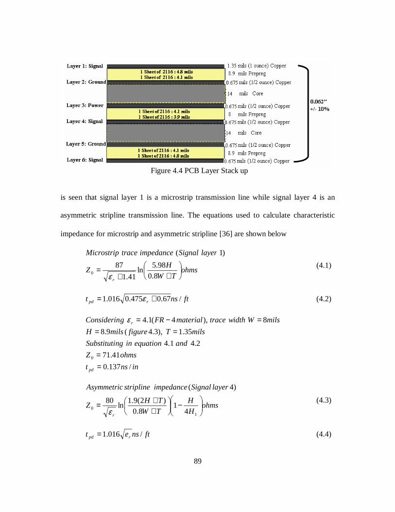
89
Figure 4.4 PCB Layer Stack up
is seen that signal layer 1 is a microstrip transmission line while signal layer 4 is an
asymmetric stripline transmission line. The equations used to calculate characteristic
impedance for microstrip and asymmetric stripline [36] are shown below
ohmsTW
HZ
layerSignalimpedancetraceMicrostrip
r
++=
8.0
98.5ln
41.1
87
)1(
0 ε (4.1)
ftnst rpd /67.0475.0016.1 += ε (4.2)
innst
ohmsZ
andequationinngSubstituti
milsTfiguremilsH
milsWwidthtracematerialFRgConsiderin
pd
r
/137.0
41.71
2.41.4
35.1),3.4(9.8
8),4(1.4
0
==
===−=ε
ohmsH
H
TW
THZ
layerSignalimpedancestriplineAsymmetric
r
−
++=
10 4
18.0
)2(9.1ln
80
)4(
ε (4.3)
ftnset rpd /016.1= (4.4)

90
innst
ohmsZ
andequationinngSubstituti
milsTmilsWmilsHmilsHfigureFrom
pd /171.0
76.50
4.43.4
675.0,8,141,84.4
0
==
====
The rise/fall time for clock signals for TMS320F2808 DSP is 2ns, GPIO pins is
8ns [37] and JTAG signals alone have rise/fall times of 500ps [38]. The trace length
beyond which transmission line effects like reflection become prominent is given by
equation (2.2). For GPIO traces (considering asymmetric stripline traces)
2 x 0.171ns/in x tracelength > 8ns
Therefore for trace lengths greater than 23.4 inches, overshoot and ringing can
occur. For JTAG signal traces, (Since asymmetric stripline, signal layer 4 has lower
impedance than microstrip, the routing is done on the former)
2 x 0.171ns/in x tracelength > 0.5ns
The maximum tracelength for JTAG signals is 1.46 inch. Hence we conclude
that JTAG signals must be analyzed for transmission line effects. Among the JTAG
signals, only TDO is an output signal. It is assumed that termination for the other
signals is provided at the driver end. Based on recommendations from TI [38], parallel
termination was provided for TCLK pin (100 ohms in series with 22pF capacitor).
The JTAG signals have an output impedance of 7 ohms [38]. Series termination
is provided to match the impedance of the source (7 ohms) and transmission line
impedance (50ohms). Using the lattice method described in chapter 2, a series
termination resistor of 33 ohms was connected to TDO pin. In figure 4.3 it is seen that
in the functional distribution block, JTAG was placed close to the DSP chip.

91
Figure 4.5 PSPICE simulation and Lattice diagram method using Excel, without
series termination
Figure 4.6 PSPICE and Excel simulation with series termination resistor

92
Figure 4.5 and 4.6 shows the simulation done in Excel (using lattice method) and
PSPICE for a low to high transition.
4.1.6 Routing
A combination of manual and auto routing was used to route the PCB.
After each route, Design Rule Check (DRC) was performed. This option is available in
OrCAD Layout and contains definitions on trace spacing, component spacing, via
spacing etc. Routing was an iterative process involving DRC and component placement
reorganization. A snapshot of the completely routed DSP board is shown in figure 4.7
Figure 4.7 Completely routed PCB
4.1.7 Preparation of gerber files, fabrication, assembly and testing
Gerber files are one of the industry standards for accepting PCB designs for
fabrication. It contains routing information for each of the layers, solder mask layers,
drill sizes etc. This file was generated using OrCAD Layout and is available in

93
Appendix B. After fabrication and assembling the components, the PCB was tested for
stability of the power signals. The integrity of the clock signals was also tested. Figure
4.8 shows the output of XCLKOUT pin of the DSP after it was powered up. The DSP
was then programmed (using JTAG) to generate PWM signals.
Figure 4.8 XCLKOUT in output of the custom DSP board after initial powerup
Figure 4.9 Output of custom DSP board generating PWM signals

94
4.2 Three Phase Inverter
The 3 phase inverter was designed given a supply DC voltage of 300V to drive
a 2kW motor. Considering Space Vector PWM, the maximum peak line to line voltage
achievable is 300V.
Hence Vmax(line-line)=300V
AII
AI
WI
PowerMotorMIV
MfactorpowermotorMefficiencymotorAssume
VV
linermslinepeak
linerms
linerms
flinermslinelinerms
fe
linelinerms
98.1077.72.2
77.7
20007.016.2123
)1.4(..3
,7.0,7.0
16.2122
300
)()(
)(
)(
)()(
)(
=×==
=
=×××
=
==
==
−
−
In order to handle worst case scenarios in which power factor exhibits lower
levels, MOSFET IRFP460PbF (VDSS=500V, ID=20A) was selected for the switches of
the inverter.
Gate drive for the MOSFETs was provided using IRF2130 3 phase bridge
driver. The key features of this driver are
1) High side can handle upto 600V.
2) Six gate drive outputs capable of supplying from 10V to 20V.
3) Compatible with CMOS and LSTTL logic inputs down to 2.5V logic.
High side gate drive supply was provided using bootstrap capacitors. The
selection of bootstrap capacitors was based on the following expression [39]

95
min
)((max)22
VVVV
f
IQ
f
IQ
CLSfcc
leakcbsls
qbsg
−−−
+++
≥ (4.2)
]41[30circuitrydriversidehighforcurrentquiescent
)50(assumecurrentleakagecapacitorBootstrap
]40[210FETsidehighofchargegate
(max)
)(
AI
AI
nCQ
where
qbs
leakcbs
g
µµ
==
==
==
VV
VV
VV
VV
Hzf
ICsVVnCQ
LS
S
f
cc
ls
1driver)highforload(orFETsidelowtheacrossdropvoltage
10VandVbetweenvoltageminimum
1diodebootstrapdropvoltageforward
15voltagesupply
)100ofminimum(assumeoperationoffrequency
)600/500(5cycleperrequiredchargeshiftlevel
Bmin
====
====
===
Substituting above values in equation 4.2, we get C > 0.816µF. Hence a 1µF
bootstrap capacitor is used. The schematics for the gate driver and 3 phase inverter is
provided in Appendix B
4.3 Simulation results
Space Vector PWM signals were simulated in MATLAB (SIMULINK). The
SVPWM line to line signals were filtered using an RC filter. Figure 4.10 shows the
equivalent RC circuit used to filter the 3 PWM signals.
Input parameters used for the simulation
1) Vdc=24V %DC bus voltage
2) fc=1e4Hz %Carrier frequency
3) fo=100Hz % fundamental frequency
4) Rfil=2e3 ohms% filter resistance value
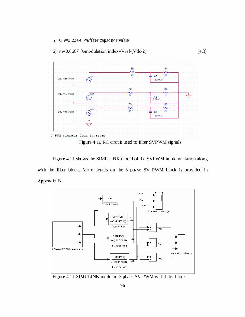
96
5) Cfil=0.22e-6F%filter capacitor value
6) m=0.6667 %modulation index=Vref/(Vdc/2) (4.3)
Figure 4.10 RC circuit used to filter SVPWM signals
Figure 4.11 shows the SIMULINK model of the SVPWM implementation along
with the filter block. More details on the 3 phase SV PWM block is provided in
Appendix B
Figure 4.11 SIMULINK model of 3 phase SV PWM with filter block

97
Figure 4.12 SVPWM line to neutral voltages
Figure 4.13 SVPWM Line to Line filtered waveforms

98
4.4 Experimental Results:
The input parameters used for the experimental setup was same as used for the
simulation (4.3). Space Vector PWM signals were generated using the custom DSP
board and provided to a 3 phase inverter. Figure 4.15 and 4.16 shows the line to neutral
and line to line filtered voltage waveforms. As seen below the experimental results
match the simulation waveforms.
4.5 Comparison of SVPWM, SPWM and SPWM with (1/6th) 3rd harmonic
SVPWM, SPWM and SPWM with one sixth 3rd harmonic were implemented in
SIMULINK. The PWM signals were regular sampled and symmetric. Total Harmonic
Figure 4.14 FFT of SVPWM (SIMULINK) Line to Line voltage Vab

99
Figure 4.15 Filtered Line to neutral voltage Van from 3 phase inverter
Figure 4.16 Filtered Line to Line voltage Vab from 3 phase inverter
Distortion of the line to line voltage (Vab) was measured using THD block of
SimPowerSystems. THD is defined as [42]

100
componentlfundamentaofvaluermsU
UUUUU
harmonicstheofvalueRMStheisUwhere
U
UTHD
n
h
h
=++++=
=
1
225
24
23
22
1
......
. (4.4)
Figure 4.17 shows the variation of THD with modulation index for each of the above
modulation schemes. We find that the THD of all the three modulation schemes are
very close to each other with SVPWM having a slightly better THD at higher
modulation index values. Note that symmetric regular sampled SPWM also provides
similar THD results in comparison with the other two modulation schemes.
THD analysis of three PWM schemes
0
0.2
0.4
0.6
0.8
1
1.2
1.4
1.6
1.8
0.4
0.45 0.5
0.55 0.6
0.65
0.67 0.7
0.75 0.8
0.85 0.9
0.95 1
1.05 1.1
1.16
modulation index
TH
D
SpaceVectorPWM
Sine+(1/6)3rd harmonic PWM
SinePWM
Figure 4.17 Comparison of THD of SVM, SPWM and SPWM with one sixth 3rd
harmonic fc/fo=10kHz/100Hz=100

101
This observation is line with the comparisons presented earlier in chapter 3.
SPWM and SVPWM have identical switching patterns and hence are expected to have
similar THD. The addition of one sixth third harmonic to SPWM only increased the
linear modulation range (m=1.15); identical to the modulation range that can be
achieved using SVPWM. Equal null pulse times (t0-t7) provided no significant
advantage in THD performance. The representation of the modulation schemes
(symmetric regular sampled PWM) plays a major role in determining THD. Hence
Sinusoidal PWM with one sixth third harmonic injection provides similar features as
Space Vector PWM, and hence is preferable due its simplicity of implementation.

102
CHAPTER 5
CONCLUSIONS AND FUTURE WORK
5.1 Conclusions
In this thesis the design and development of an embedded DSP controller was
presented. The concepts on high speed PCB design were presented in Chapter 2. The
DSP board was designed to use all the features of the TMS320F2808. During initial
layout the board was divided into functional components. Though PCB design tools
have the auto place feature, it is not used since manual placement is easier and better
control of trace lengths can be achieved. The board had a single ground for both analog
and digital signals with the analog section separated from the digital section. This was
based on the fact that the return path for high frequency signals lies right beneath the
trace. JTAG signals, with rise time of 500ps were found to be most sensitive to trace
length. Series termination was provided to match the impedance of source and the trace.
In the second part of the thesis, a three phase inverter was designed. Space
Vector PWM signals were generated using the DSP board and tested on the three phase
inverter. It is seen that generation of Space Vector signals involves calculation of duty
cycle times based on the sector of a rotating reference vector signal. This modulation
scheme is known to better utilize the DC bus voltage and produce lesser Total
Harmonic Distortion. A comparison between Sinusoidal PWM with one sixth third
harmonic injection and Space Vector PWM has shown that the former modulation

103
scheme produces similar results as Space Vector and is favorable due to its simplicity of
implementation.
5.2 Future work
The integration of power application devices like inverters, DC/DC converters
on a single DSP controller board is an area for future work. This will involve careful
considerations for separating power signals from electronic high frequency of the DSP.
Reduced size, EMI/EMC and tolerance to external influences like vibrations are factors
that would be challenging in designing an integrated DSP controller board. This would
enable its pervasive use in home appliances and automotive industry.

104
APPENDIX A
DSP BOARD SCHEMATICS AND LAYOUT

105
+ C71uF
Lithium Battery
C90.1uF
ADCINB6
ADCINB2
GPIO19
Y1
ABS07-32.768KHz
R12.2K
ADCINA7
R10
4.99K
XTDI
3.3V
ADCINA1
R90
GPIO27
R6
4.99K
GPIO23
1.8V
5V
GPIO0
GPIO31
ADCINB3GPIO8
GPIO16
GPIO4
GPIO12
C50.1uF
R5
10K
VREFLO
VDD3VFL
U5
LM4040/SOT23
21
GPIO20
GND
+ C41uF
ADCINB0
R152.0K
SINGLE POINT CONNECTION
L2
BLM21P221SN
ADCINA2
XTMS
GPIO34
R7
4.99K
GPIO28R11 4.99K
GPIO24
GPIO5
XTRST
SCLA
C30.1uF
GPIO1
GPIO32
1.8V
R14
0
GPIO9ADCINB4
U4
REF3020AIDBZT
13
2
INGND
VOUT
GPIO17
ADCINA5
GPIO13
SDAASCLA
TP1
TP
1
3.3V
GPIO25
VDD2A18
GPIO21
AGND
VDDA1.8V
C80.1uF
SDAA
C60.001uF
ADCINA3
ADCREFIN
GPIO29
C2
2.2uF CERAMIC LOW ESR
R13
1.5K
R12
0
XEMU0
R22.2K
GPIO2
GPIO6
VDDA3.3V
ADCREFIN
J1
HEADER 1
1
GPIO33
PONRSnIN
ADCREFM
GPIO10
J2
HEADER 2X1
1 2
L1
BLM21P221SN
ADCINB5
ADCINB1
GPIO18
R32.2K
C1
2.2uF CERAMIC LOW ESR
ADCINA6
GPIO14
U3
DS1307/SO
4
7
5
1
2
63
8
GND
SQW/OUT
SDA
X1
X2
SCLVBAT
VCCXTCK
VDDA3.3V
GPIO26
U1A
SYM 1 OF 2
?
?TMS320f2808PZA
72
66
84
164417
181920
38
21
8
2223
8180
67
78
60
100
76
74 7173
70
43
51
4
91
56
61
48
7
92
53
64
45
54
95
50
5
52
75
6
9
47
3433
24
32
86
31
88
3029
98
28
97
79
27
58
5763
137
99
83
36
35
90
963
466582
104259688593
211414955626977878994
2625
1240
1339
1514
GPIO23/EQEP1I/SPISTEC/SCIRXB
XCLKOUT
TRST
ADCINA7GPIO1/EPWM1B/SPISIMODADCINA6
ADCINA5ADCINA4ADCINA3
ADCRESEXT
ADCINA2
GPIO14/TZ3/SCITXB/SPICLKB
ADCINA1ADCINA0
EMU1EMU0
GPIO21/EQEP1B/SPISOMIC/CANRXB
XRS
GPIO8/EPWM5A/CANTXB/ADCSOCAO
GPIO32/SDAA/EPWMSYNCI/ADCSOCAO
TDO
TMS GPIO22/EQEP1S/SPICLKC/SCITXBTDI
GPIO11/EPWM6B/SCIRXB/ECAP4
GPIO34
GPIO4/EPWM3A
GPIO29/SCITXDA/TZ6
GPIO25/ECAP2/EQEP2B/SPISOMIB
GPIO6/EPWM4A/EPWMSYNCI/EPWMSYNCO
GPIO9/EPWM5B/SCITXB/ECAP3
GPIO3/EPWM2B/SPISOMID
GPIO31/CANTXA
GPIO28/SCIRXDA/TZ5
GPIO5/EPWM3B/SPICLKD/ECAP1
GPIO10/EPWM6A/CANRXB/ADCSOCBO
GPIO2/EPWM2A
GPIO18/SPICLKA/SCITXB
GPIO13/TZ2/CANRXB/SPISOMIB
GPIO16/SPISIMOA/CANTXB/TZ5
GPIO33/SCLA/EPWMSYNCO/ADCSOCBO
GPIO17/SPISOMIA/CANRXB/TZ6
TCK
GPIO30/CANRXA
GPIO15/TZ4/SCIRXB/SPISTEB
GPIO0/EPWM1A
ADCINB7ADCINB6
ADCLO
ADCINB5
X2
ADCINB4
X1
ADCINB3ADCINB2
TEST2
ADCINB1
TEST1
GPIO27/ECAP4/EQEP2S/SPISTEB
ADCINB0
GPIO7/EPWM4B/SPISTED/ECAP2
GPIO19/SPISTEA/SCIRXBGPIO20/EQEP1A/SPISIMOC/CANTXB
GPIO12/TZ1/CANTXB/SPISIMOBADCREFP
GPIO26/ECAP3/EQEP2I/SPICLKB
GPIO24/ECAP1/EQEP2A/SPISIMOB
ADCREFM
ADCREFIN
XCLKIN
VDD3VFLVDDIO1VDDIO2VDDIO3VDDIO4
VDD2VDD3VDD4VDD5VDD6VDD7
VSS2VSS3VSS4VSS5VSS6VSS7VSS8VSS9VSS10VSS11VSS12
VDDAIOVSSAIO
VDD1A18VDD2A18
VSS1AGNDVSS2AGND
VDDA2VSSA2
GPIO22
VDDA1.8V
XTDO
GPIO29
ADCINA4
ADCINB7
R8
22.1K
GPIO30
C100.001uF
3.3V
ADCINA0
XEMU1
R4
100K
BT1 3V
GPIO7
G1 1.0
TMS320F2808 Custom Ev aluation Board
B
1 5Thursday , July 28, 2005
Tit le
Size Document Number Rev
Date: Sheet of
GPIO3
GPIO15
GPIO18
SW1
SW DIP-6/SM
3.3V
GPIO34
3.3V
ADCREFP
U2
24LC256/SO
4
8
5
6
1
2
3
7
GND
VCC
SDA
SCL
A0
A1
A2
WP
GPIO11
XCLKIN
Figure A.1 OrCAD schematic: DSP interface with EEPROM, RTC and analog inputs

106
ADCIN_B1
GPIO12GPIO20
GPIO17
RN13
RN100K
12345
678
MUX_GPIO29
ADCIN_B10
SEQ_SELECT_1
GPIO2
CAN_RXB
SEQ_SELECT_1
GPIO28
GPIO11GPIO6
VREFLO
ADCIN_B5
GPIO7
GPIO3
GPIO29
GPIO16
MUX_GPIO11
GPIO34
ADCINB7
GPIO21
ADCIN_B11
RN12
RN100K
12345
678
ADCIN_B15
MUX_GPIO9
M
RN14
RN100K
12345
678
ADCINA6
ADCINB3
3.3V
GND
UART_RXDB
ADCIN_B2
SEQ_SELECT_1
ADCIN_B7
ADCIN_B8
MUX_GPIO30
GPIO8
GPIO18
GPIO32
UART_RXDA
M
3.3V
MUX_GPIO10
GPIO29
R190
ADCIN_B6
MUX_GPIO8
ADCIN_B13
J8
CONN TRBLK 10x2
13579
1113151719
2468101214161820
ADCIN_B10
RN17
RN100K
12345
678
3.3V
UART_TXDA
GPIO6
GPIO23
L
GPIO14
ADCINB4
GPIO30
ADCREFM
ADCIN_B16
MUX_GPIO22
GPIO16
GPIO1
L
GPIO4
SW2
SW DIP-4/SM
ADCINA3
GPIO28GPIO13
GPIO15
ADCIN_B13
GPIO5
U10
LM4040/SOT23 DCIM 3-4.1V21
ADCINA0
ADCIN_B5
GPIO0
ADCIN_B12 U11
SN74CBT3257PW
2356
13141011
8
16
115
4
7
9
12
1B11B22B12B2
4B24B13B23B1
GND
VCC
SOE'
1A
2A
3A
4A
ADCIN_B2
GPIO33 GPIO8
Pullup resistors on all the GPIO pins
GPIO26
GPIO25
ADCINA7
U13
SN74CBT3257PW
2356
13141011
8
16
115
4
7
9
12
1B11B22B12B2
4B24B13B23B1
GND
VCC
SOE'
1A
2A
3A
4A
MUX_GPIO11
ADCIN_B3
GPIO22
ADCIN_B9
UART_TXDB
CAN_TXB
GPIO10
ADCIN_B16
G1 1.0
TMS320F2808 Custom Ev aluation Board
B
4 5Thursday , July 28, 2005
Title
Size Document Number Rev
Date: Sheet of
MUX_GPIO28
GPIO30
GPIO20
GPIO23
GPIO1
GPIO7
GPIO27
RN16
RN100K
12345
678
ADCINB5
ADCIN_B3
GPIO2 is used to select between analog input channels 'L' and 'M' under software control.
GPIO3
GPIO9
3.3V
GPIO26
MUX_GPIO10
ADCINA4
GPIO31
ADCIN_B14
RN18
RN100K
12345
678
GPIO18GPIO17
RN15
RN100K
12345
678
5VADCINA1
ADCIN_B6
GPIO2
ADCINB0
GPIO31
ADCIN_B12
GPIO12
GPIO19
J12JUMPER 1
2
3
ADCIN_B1
GPIO4
ADCIN_B4 ADCINB1
GPIO21
J9
JUMPER
1 2
3
GPIO0
GPIO24
R18
1.5K
J11JUMPER
12
3
MUX_GPIO8
CAN_TXA
GPIO9
GPIO10
J10
HEADER 20x2/SM
2468
10121416182022242628303234363840
13579111315171921232527293133353739
GPIO13
GPIO19
3.3V
AGND
GPIO15
ADCIN_B11
ADCIN_B14
U17
T S3 A5018
3
46
11
139
1
25
10
12
8
16
7
1415
NO1
COM1NO2
NC3
NO4COM3
IN
NC1NC2
NO3
COM4
GND
V+
COM2
NC4EN
ADCINB6
GPIO11
ADCIN_B4
GPIO5
J7
CONN TRBLK 10x2
13579
1113151719
2468101214161820
5V
RN6
RN10K
1 2 3 45678
GPIO2
ADCINA5
ADCREFP
MUX_GPIO9
ADCIN_B15
GPIO14
C18
0.1uF
MUX_GPIO31
ADCIN_B7
ADCINA2
CAN_RXA
ADCIN_B8
MUX_GPIO22GPIO25
MUX_GPIO29
RN19
RN100K
12345
678
MUX_GPIO28
MUX_GPIO30
MUX_GPIO31
U1 6
T S3A50 18
3
46
11
139
1
25
10
12
8
16
7
1415
NO1
COM1NO2
NC3
NO4COM3
IN
NC1NC2
NO3
COM4
GND
V+
COM2
NC4EN
GPIO27
ADCIN_B9ADCINB2
Figure A.2 OrCAD schematic: analog multiplexer, GPIO interface

107
C14 0.1uF
PCRXDB
PCRXDA
J6
HEADER 5X2
246810
13579
UART_TXDB
C16
0.1uF
3.3V
RN2RN20K
1 2 3 45678
C170.1uF
UART_RXDAUART_RXDB
C150.1uF
C130.1uF
UART_TXDA
PCTXDB
G1 1.0
TMS320F2808 Custom Ev aluation Board
B
3 5Thursday, July 28, 2005
Title
Size Document Number Rev
Date: Sheet of
U8
MAX3238/SO
226
16
152825
13
27 4
1314
2423221917
891121
2018
5671012
GNDVCC
R1OUTB
INVALIDC1+C1-
C2+C2-
V+ V-
FORCEONFORCEOFF
T1INT2INT3INT4INT5IN
R1INR2INR3INR1OUT
R2OUTR3OUT
T1OUTT2OUTT3OUTT4OUTT5OUT
P2
DB9F
594837261
PCTXDA
GND
3.3V
Figure A.3 OrCAD schematic: SCI interface
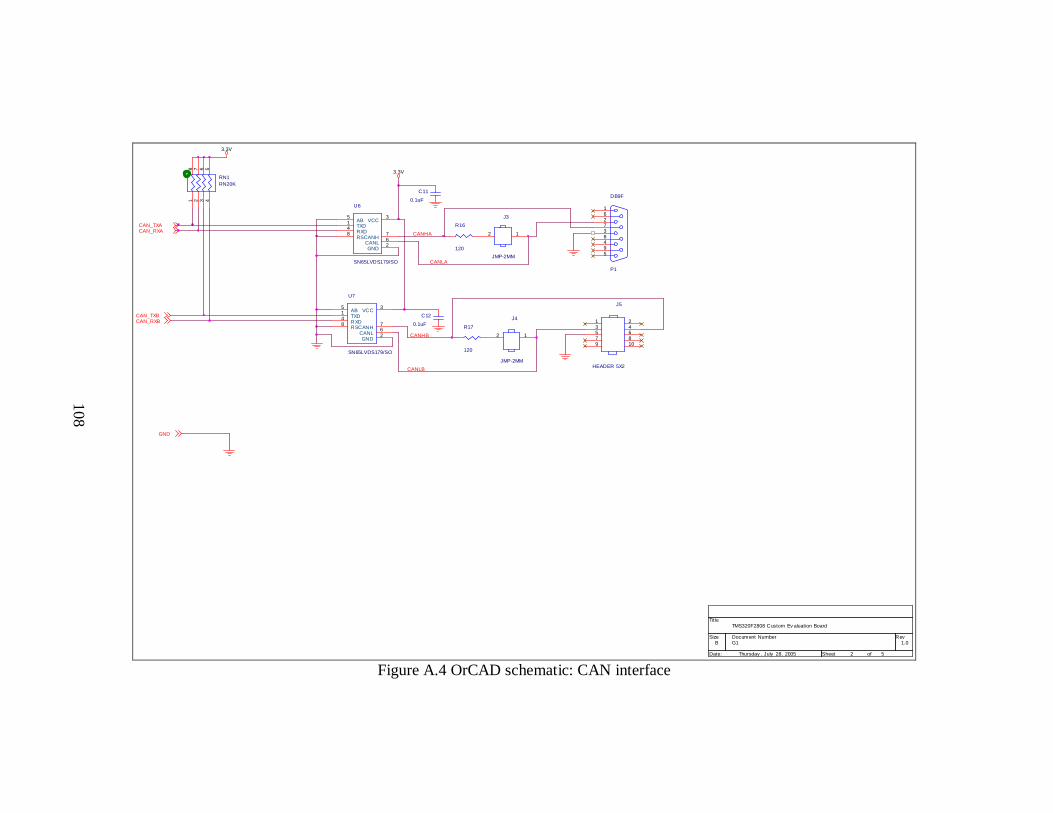
108
J3
JMP-2MM
12
CAN_TXB
C11
0.1uF
R16
120
U6
SN65LVDS179/SO
3
6
1
2
5
784
VCC
CANL
TXD
GND
AB
CANHRSRXD
3.3V
J5
HEADER 5X2
246810
13579
CAN_RXA
R17
120
RN1RN20K
1 2 3 45678
G1 1.0
TMS320F2808 Custom Ev aluation Board
B
2 5Thursday , July 28, 2005
Tit le
Size Document Number Rev
Date: Sheet of
J4
JMP-2MM
12
CAN_RXB
CANLB
C12
0.1uF
GND
CANLA
CANHA
U7
SN65LVDS179/SO
3
6
1
2
5
784
VCC
CANL
TXD
GND
AB
CANHRSRXD
CANHB
3.3V
CAN_TXA
P1
DB9F
594837261
Figure A.4 OrCAD schematic: CAN interface

109
TCK
XTDI
Q1BSS138/SOT
Thermal Pad
3.3V
3.3V
U18SN74LVC1G32DB
2
4
3
1
5
B
Y
GN
D
A
VC
C
1.8V
3.3V
C200.1uF
1.8V
C440.1uF
C430.1uF
R27
1.5K 1%
C3922uF
C360.1uF
C300.1uF
XTDO
C1947uF
R22
30.1k
C370.1uF
R34
10k
+ C450.1uF
3.3V
C410.1uF
5V
R23
10K
C2922uF
C380.1uF
XCLKIN
XTRST
R31
10k
C220.1uF
C230.1uF
R25
0
R20220
3.3V
5V
D1
LTST-C150GKT (GREEN)
GND
R24
0
R29
100
C250.1uF
J17
JUMPER
1 2
3
C420.1uF
R30
10k
R28
2.0K 1%
XTCK
C350.1uF
XTPDR32
33
C270.1uF
C340.1uF
G1 1
TMS320F2808 Custom Evaluation Board
B
5 5Friday , August 05, 2005
Title
Size Document Number Rev
Date: Sheet of
3.3V
C2122uf
J16
HEADER 7x2/SM
2468
101214
135791113
J14
+5V Max
123
C4722pF
R36
10k
L3
BLM21P221SN
XTMS
R2116.9k
U14
C78L52/TO92
2
4
3
1
GND
VCC
CLK
OFFn
+ C261uF
C2422uF
Near DSP TCK pin
VDD3VFL
R35
10k
XEMU0
C310.1uF
C320.1uF
3.3V
C2822uF
Near DSP TCK pin
J15
HEADER 1
1
JTAG 14-pin header connections
C330.1uF
PONRSnIN
C400.1uF
R2610k
+ C460.1uF
3.3V
RASM712
TPS767D301
9
19
12
25
11
16
151413
65
27
18
26
17
28
2120
4
87
2423
10
21
3
22
X2GND
NC19
X2IN12
X1FB/NC
X2IN11
NC16
NC15NC14NC13
X1IN6X1IN5
NC27
X2OUT18
NC26
X2OUT17
X1RESET*
NC21NC20
X1EN*
NC8NC7
X1OUT24X1OUT23
X2EN*
NC2NC1
X1GND
X2RESET*
R33
10k
R37100
XEMU1
Figure A.5 OrCAD schematic: Power system, JTAG interface

110
Figure A.6 OrCAD Layout: Silkscreen layer

111
Figure A.7 OrCAD Layout: Top layer (1)

112
Figure A.8 OrCAD Layout: Ground layer (2)

113
Figure A.9 OrCAD Layout: Power layer (3)

114
Figure A.10 OrCAD Layout: Signal layer (4)

115
Figure A.11 OrCAD Layout: Ground layer (5)

116
Figure A.12 OrCAD Layout: Bottom layer (6)

117
APPENDIX B
BILL OF MATERIALS

118
Serial No Title Mfr Name Mfr P/N Package
OrCAD Layout Footprint Comments
1 IC, QFP100, DSP, TMS320F2808 Texas Instruments TMS320F2808 PQFP-G100 quad0.5M/100/wg16.10 U1
2 IC,SO8, SERIAL EEPROM, 256K-BIT Catalyst Semiconductor Inc CAT24WC256J
8-Lead 150 Mil Wide SOIC (J,W) sog.050/8/wg.244/l.200 U2
3 IC,TSOP28, RS-232 TRANSCEIVER, 10nA Texas Instruments MAX3238CPW 28-SOIC sog.050/28/wg.420/l.725 U8
4
IC, SOT23, CMOS VOLTAGE REFERENCE, 2.048V Texas Instruments REF3020AIDBZT SOT-23 (DBZ)| 3 sm/sot23_123 U4
5 IC, SO8, TRANSCEIVER, 3.3V Texas Instruments SN65HVD230D SOIC (D)|8 sog.050/8/wg.244/l.200 U6 U7
6 IC,QSOP16,QUAD 2:1 MUX/DEMUX Texas Instruments SN74CBT3257D 16-SOIC sog.050/16/wg.244/l.400 U11 U13
7 IC, SSOP28, DUAL LOW DROP OUT VOLTAGE REGULATOR Texas Instruments TPS767D301PWP HTSSOP(PWP)|28 htssop_pwp_28 TPS767D301
8 OSC, SMT, 24MHZ CTS Electronics Corporation
CB3LV-3C-20.000-T SMT (Custom)|4 sm_osc20Mhz_4pin
9
TRANSISTOR, SOT23, MOSFET, N-CHANNEL , BSS138 ZETEX INC BSS138TA SOT-23 (DBZ)| 3 sm/sot23_123 Q1
10 DIODE, SOT23, REFERENCE, 2.5V National Semiconductor LM4040CIM3-2.5 SOT-23 (DBZ)| 3 sm/sot23_123 U5
11 DIODE, SOT23, REFERENCE, 4.1V National Semiconductor LM4040CIM3X-4.1 SOT-23 (DBZ)| 3 sm/sot23_123 U10
12 LED, SMT 1206, GREEN LITEON LTST-C150GKT SMT |2 sm/d_1206 D1
13 DIODE, MELFM ZENER, 6.2V, 500mW DIODES Inc ZMM5234B SOD-80, mini MELF sod80_minimelf
14 FERRITE BEAD, SMT 0805, 220 OHMS Murata Electronics BLM21PG221SN1D SMT|2 smb/l_0805 L1 L2 L3
15 CAP, CER, SMT 1206, 1uF, 16V, +/-20%, X7R AVX Corporation 1206YC105MAT2A smb/c_1206 C4 C7 C26
16 CAP, TANT, SMT 1311, 22uF, 6.3V PANASONIC ECS-T0JX226R SMT sm/c_tant1311 C21 C24
17 CAP, TANT, SMT 2816, 47uF, 10V PANASONIC ECS-T1AD476R SMT sm/c_tant2816 C19
18 CAP, CER, SMT 1206, 0.022uF, 50V, +/-10%, X7R PANASONIC ECU-V1H223KBM SMT sm/c_1206
19 CAP, CER, SMT 0805, 2.2uF, 10V TAIYO YUDEN LMK212BJ225KG-T SMT smb/c_0805 C1 C2
20 CAP, CER, SMT 0603, 22pF, 50V , +/-5%, NPO PANASONIC ECU-V1H220JCV SMT sm/c_0603 C47

119
21 CAP, CER, SMT 0603, 0.001uF, 50V, +/-10%, X7R AVX Corporation 06035C102KAT2A SMT sm/c_0603 C6 C10
22 CAP, CER, SMT 0603, 0.1uF, 16V, +/-10%, X7R
KEMET Electronics Corporation C0603C104K4RAC SMT sm/c_0603
C3 C5 C8 C9 C18 C13 C15C16 C17 C14 C11 C12 C20 C23 C22 C25 C27 C30 C31 C32 C33 C34 C35 C36 C37 C38 C40 C41 C42 C43 C44 C45 C46
23 RES, NETWORK, SMT, 8 PIN, 4 RES, 20K OHM, 5%, 1/16 WATT PANASONIC EXB-28V203JX SMT|8 smt_rn8pin RN2
24 RES, NETWORK, SMT, 8 PIN, 4 RES, 100K OHM, 5%, 1/16 WATT PANASONIC EXB-28V104JX SMT|8 smt_rn8pin
RN12 RN13 RN14 RN15 RN16 RN17 RN18 RN19
25 RES, SMT 1206 , 121 OHM, 1%, 1/8 WATT PANASONIC ERJ-8ENF1210V SMT sm/r_1206 R16 R17 R24 R25
26 RES, SMT 0603 , 0 OHM, 1%, 1/16 WATT KOA SPEER ELECTRONICS, INC RM73Z1J000 SMT smb/r_0603
R9 R14 R12 R25
27 RES, SMT 0603 , 220 OHM, 1%, 1/16 WATT PANASONIC ERJ-3GSYJ221V SMT sm/r_0603 R20
28 RES, SMT 0603 , 33 OHM, 1%, 1/16 WATT KOA SPEER ELECTRONICS, INC RM73B1JT33RJ SMT sm/r_0603
29 RES, SMT 0603 , 2.2K OHM, 1%, 1/16 WATT PANASONIC ERJ-3GEYJ222V SMT sm/r_0603 R1 R2 R3
30 RES, SMT 0603 , 22K OHM, 1%, 1/16 WATT PANASONIC ERJ-3GEYJ223V SMT smb/r_0603 R8
31 RES, SMT 0603 , 100 OHM, 1%, 1/16 WATT
ROHM CORPORATION MCR03F1000EZP SMT sm/r_0603 R29 R37
32 RES, SMT 0603 , 20K OHM, 1%, 1/16 WATT PANASONIC ERJ-3EKF2002V SMT sm/r_0603
33 RES, SMT 0603 , 1.5K OHM, 1%, 1/16 WATT PANASONIC ERJ-3EKF1501V SMT sm/r_0603 R13 R18 R27
34 RES, SMT 0603 , 10K OHM, 1%, 1/16 WATT PANASONIC ERJ-3EKF1002V SMT sm/r_0603
R23 R26 R35 R34 R31 R33 R36 R30
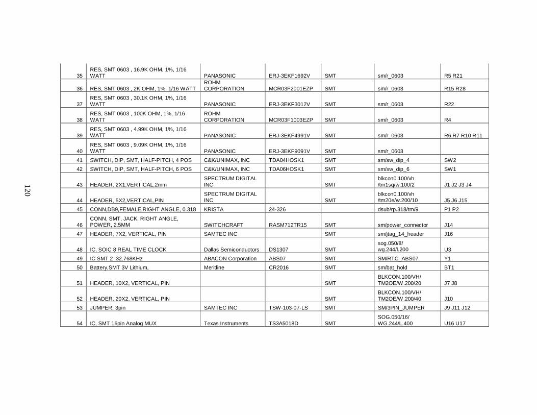
120
35 RES, SMT 0603 , 16.9K OHM, 1%, 1/16 WATT PANASONIC ERJ-3EKF1692V SMT sm/r_0603 R5 R21
36 RES, SMT 0603 , 2K OHM, 1%, 1/16 WATT ROHM CORPORATION MCR03F2001EZP SMT sm/r_0603 R15 R28
37 RES, SMT 0603 , 30.1K OHM, 1%, 1/16 WATT PANASONIC ERJ-3EKF3012V SMT sm/r_0603 R22
38 RES, SMT 0603 , 100K OHM, 1%, 1/16 WATT
ROHM CORPORATION MCR03F1003EZP SMT sm/r_0603 R4
39 RES, SMT 0603 , 4.99K OHM, 1%, 1/16 WATT PANASONIC ERJ-3EKF4991V SMT sm/r_0603 R6 R7 R10 R11
40 RES, SMT 0603 , 9.09K OHM, 1%, 1/16 WATT PANASONIC ERJ-3EKF9091V SMT sm/r_0603
41 SWITCH, DIP, SMT, HALF-PITCH, 4 POS C&K/UNIMAX, INC TDA04HOSK1 SMT sm/sw_dip_4 SW2
42 SWITCH, DIP, SMT, HALF-PITCH, 6 POS C&K/UNIMAX, INC TDA06HOSK1 SMT sm/sw_dip_6 SW1
43 HEADER, 2X1,VERTICAL,2mm SPECTRUM DIGITAL INC SMT
blkcon0.100/vh /tm1sq/w.100/2 J1 J2 J3 J4
44 HEADER, 5X2,VERTICAL,PIN SPECTRUM DIGITAL INC SMT
blkcon0.100/vh /tm20e/w.200/10 J5 J6 J15
45 CONN,DB9,FEMALE,RIGHT ANGLE, 0.318 KRISTA 24-326 dsub/rp.318/tm/9 P1 P2
46 CONN, SMT, JACK, RIGHT ANGLE, POWER, 2.5MM SWITCHCRAFT RASM712TR15 SMT sm/power_connector J14
47 HEADER, 7X2, VERTICAL, PIN SAMTEC INC SMT sm/jtag_14_header J16
48 IC, SOIC 8 REAL TIME CLOCK Dallas Semiconductors DS1307 SMT sog.050/8/ wg.244/l.200 U3
49 IC SMT 2 ,32.768KHz ABACON Corporation ABS07 SMT SM/RTC_ABS07 Y1
50 Battery,SMT 3V Lithium, Meritline CR2016 SMT sm/bat_hold BT1
51 HEADER, 10X2, VERTICAL, PIN SMT BLKCON.100/VH/ TM2OE/W.200/20 J7 J8
52 HEADER, 20X2, VERTICAL, PIN SMT BLKCON.100/VH/ TM2OE/W.200/40 J10
53 JUMPER, 3pin SAMTEC INC TSW-103-07-LS SMT SM/3PIN_JUMPER J9 J11 J12
54 IC, SMT 16pin Analog MUX Texas Instruments TS3A5018D SMT SOG.050/16/ WG.244/L.400 U16 U17

121
APPENDIX C
SIMULINK SPACE VECTOR PWM BLOCK DIAGRAM

122
Figure C.1 Simulink model: Space Vector implementation [32]
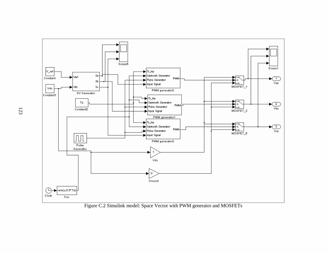
123
Figure C.2 Simulink model: Space Vector with PWM generator and MOSFETs
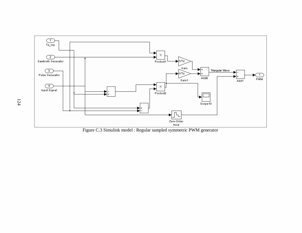
124
Figure C.3 Simulink model : Regular sampled symmetric PWM generator

125
Figure C.4 Simulink model: RC filtered line to line voltage generation

126
APPENDIX D
THREE PHASE INVERTER SCHEMATICS

127
Figure D.1 IR2130 gate driver schematic [43]
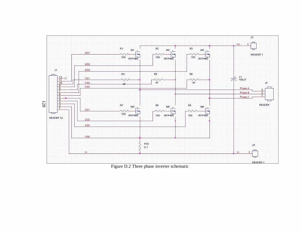
128
Figure D.2 Three phase inverter schematic

129
APPENDIX E
SPACE VECTOR PWM CODE

130
//************************************************* **************************** // // FILE: VSI_SpaceVectorPWM.c // // TITLE: This program generates Space Vector PWM signals on outputs // ePWM1,ePWM2 and ePWM3 // // // DESCRIPTION: //************************************************* **************************** // Developer: Harish Raman // Created on: 18th Jan, 2006; // Updated on: 4th Mar 2006 // Changes done: 1) corrected error in sector times // 2) changed PWM frequency to 10kHz // (enhanced PWM generation code obtained from TI 2 80x examples) //************************************************* **************************** #include "DSP280x_Device.h" // DSP280x Headerfi le Include File #include "DSP280x_Examples.h" // DSP280x Examples Include File #include "math.h" // Prototype statements for functions found within this file. void InitEPwm1(void); void InitEPwm2(void); void InitEPwm3(void); void InitSpaceVector(void); interrupt void epwm1_isr(void); interrupt void epwm2_isr(void); interrupt void epwm3_isr(void); // Global variables used in this example Uint32 EPwm1TimerIntCount; Uint32 EPwm2TimerIntCount; Uint32 EPwm3TimerIntCount; Uint16 iFund_freq; // fundamental frequency of re quired output Uint16 iV_Ref; // reference voltage - peak voltag e of output Uint16 iV_Dc; // DC bus voltage float fTz; // sampling period float fTz_incr; // temp variable to store temp i ncrement of Tz

131
float fAlpha; // angle of space vector int iSector; // sector number float fT0; // time T0; float fT1; // time T1; float fT2; // time T2; float fS0; // time of Switch 1(fS0/fTz=duty cy cle for ePWM1) float fS1; // time of Switch 2(fS1/fTz=duty cy cle for ePWM2) float fS2; // time of Switch 3(fS2/fTz=duty cy cle for ePWM3) float fTempCoeff; // temp variable float fTempArr[200]; float ftemp; int i=0; #define PI 3.142 void main(void) // Step 1. Initialize System Control: // PLL, WatchDog, enable Peripheral Clocks // This example function is found in the DSP280x_Sy sCtrl.c file. InitSysCtrl(); // Step 2: // For this case just init GPIO pins for ePWM1, ePW M2, ePWM3 // These functions are in the DSP280x_EPwm.c file InitEPwm1Gpio(); InitEPwm2Gpio(); InitEPwm3Gpio(); // Step 3. Clear all interrupts and initialize PIE vector table: // Disable CPU interrupts DINT; // Initialize the PIE control registers to their de fault state. // The default state is all PIE interrupts disabled and flags // are cleared. // This function is found in the DSP280x_PieCtrl.c file. InitPieCtrl(); // Disable CPU interrupts and clear all CPU interru pt flags: IER = 0x0000;

132
IFR = 0x0000; // Initialize the PIE vector table with pointers to the shell Interrupt // Service Routines (ISR). // This will populate the entire table, even if the interrupt // is not used in this example. This is useful for debug purposes. // The shell ISR routines are found in DSP280x_Defa ultIsr.c. // This function is found in DSP280x_PieVect.c. InitPieVectTable(); // Interrupts that are used in this example are re- mapped to // ISR functions found within this file. EALLOW; // This is needed to write to EALLOW pr otected registers PieVectTable.EPWM1_INT = &epwm1_isr; PieVectTable.EPWM2_INT = &epwm2_isr; PieVectTable.EPWM3_INT = &epwm3_isr; EDIS; // This is needed to disable write to E ALLOW protected registers // Step 4. Initialize all the Device Peripherals: // This function is found in DSP280x_InitPeripheral s.c // InitPeripherals(); // Not required for this exa mple EALLOW; SysCtrlRegs.PCLKCR0.bit.TBCLKSYNC = 0; EDIS; // Initialize space vector PWM variables InitSpaceVector(); InitEPwm1(); InitEPwm2(); InitEPwm3(); EALLOW; SysCtrlRegs.PCLKCR0.bit.TBCLKSYNC = 1; EDIS; // Step 5. User specific code, enable interrupts // Initalize counters: EPwm1TimerIntCount = 0; EPwm2TimerIntCount = 0;

133
EPwm3TimerIntCount = 0; // Enable CPU INT3 which is connected to EPWM1-3 IN T: IER |= M_INT3; // Enable EPWM INTn in the PIE: Group 3 interrupt 1 -3 PieCtrlRegs.PIEIER3.bit.INTx1 = 1; PieCtrlRegs.PIEIER3.bit.INTx2 = 1; PieCtrlRegs.PIEIER3.bit.INTx3 = 1; // Enable global Interrupts and higher priority rea l-time debug events: EINT; // Enable Global interrupt INTM ERTM; // Enable Global realtime interrupt DBGM // Step 6. IDLE loop. Just sit and loop forever (op tional): for(;;) asm("NOP"); // This interrupt implements the Space vector algor ithm // During every interrupt the times T0,T1 and T2 ar e calculated // Based on the sector number, the switching times S1,S2 and S3 are // calculated. interrupt void epwm1_isr(void) if(fAlpha>6.28) // check if alpha >2*pi radians fTz_incr=0; fAlpha=2*PI*iFund_freq*fTz_incr; // fAlpha = 0-2P I iSector=floor(fAlpha/(PI/3)); fT1=fTempCoeff*sin(((iSector+1)*(PI/3))-fAlpha); fT2=fTempCoeff*sin(fAlpha-(iSector*(PI/3))); fT0=fTz-fT1-fT2; //Determine switching times if(iSector==0) fS0=(fT0/2)+fT1+fT2;

134
fS1=(fT0/2)+fT2; fS2=(fT0/2); else if(iSector==1) fS0=(fT0/2)+fT1; fS1=(fT0/2)+fT1+fT2; fS2=(fT0/2); else if(iSector==2) fS0=(fT0/2); fS1=(fT0/2)+fT1+fT2; fS2=(fT0/2)+fT2; else if(iSector==3) fS0=(fT0/2); fS1=(fT0/2)+fT1; fS2=(fT0/2)+fT2+fT1; else if(iSector==4) fS0=(fT0/2)+fT2; fS1=(fT0/2); fS2=(fT0/2)+fT1+fT2; else if(iSector==5) fS0=(fT0/2)+fT1+fT2; fS1=(fT0/2); fS2=(fT0/2)+fT1; // updating duty cycles of ePWM1,ePWM2, ePWM3 ftemp=(fS0/fTz); ftemp=ftemp*EPwm1Regs.TBPRD; // storing in array only to test SV waveform on Co de Composer fTempArr[i++]=ftemp;
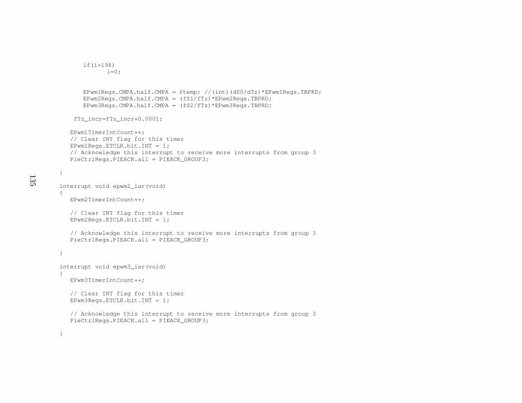
135
if(i>198) i=0; EPwm1Regs.CMPA.half.CMPA = ftemp; //(int)(dS0/dTz) *EPwm1Regs.TBPRD; EPwm2Regs.CMPA.half.CMPA = (fS1/fTz)*EPwm2Regs.TBP RD; EPwm3Regs.CMPA.half.CMPA = (fS2/fTz)*EPwm3Regs.TBP RD; fTz_incr=fTz_incr+0.0001; EPwm1TimerIntCount++; // Clear INT flag for this timer EPwm1Regs.ETCLR.bit.INT = 1; // Acknowledge this interrupt to receive more in terrupts from group 3 PieCtrlRegs.PIEACK.all = PIEACK_GROUP3; interrupt void epwm2_isr(void) EPwm2TimerIntCount++; // Clear INT flag for this timer EPwm2Regs.ETCLR.bit.INT = 1; // Acknowledge this interrupt to receive more in terrupts from group 3 PieCtrlRegs.PIEACK.all = PIEACK_GROUP3; interrupt void epwm3_isr(void) EPwm3TimerIntCount++; // Clear INT flag for this timer EPwm3Regs.ETCLR.bit.INT = 1; // Acknowledge this interrupt to receive more in terrupts from group 3 PieCtrlRegs.PIEACK.all = PIEACK_GROUP3;
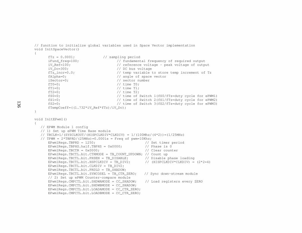
136
// function to initialize global variables used in Space Vector implementation void InitSpaceVector() fTz = 0.0001; // sampling period iFund_freq=100; // fundamental frequency of requ ired output iV_Ref=100; // reference voltage - peak voltage of output iV_Dc=300; // DC bus voltage fTz_incr=0.0; // temp variable to store temp in crement of Tz fAlpha=0; // angle of space vector iSector=0; // sector number fT0=0; // time T0; fT1=0; // time T1; fT2=0; // time T2; fS0=0; // time of Switch 1(fS0/fTz=duty cycle for ePWM1) fS1=0; // time of Switch 2(fS1/fTz=duty cycle for ePWM2) fS2=0; // time of Switch 3(fS2/fTz=duty cycle for ePWM3) fTempCoeff=((1.732*iV_Ref*fTz)/iV_Dc); void InitEPwm1() // EPWM Module 1 config // 1) Set up ePWM Time Base module // TBCLK=1/(SYSCLKOUT/(HISPCLKDIV*CLKDIV) = 1/(1 00Mhz/(4*2))=(1/25MHz) // TPWM = 2*TBPRD/(25MHz)=0.0001s = Freq of pwm= 10Khz; EPwm1Regs.TBPRD = 1250; // Set timer period EPwm1Regs.TBPHS.half.TBPHS = 0x0000; // Phase is 0 EPwm1Regs.TBCTR = 0x0000; // Clear counter EPwm1Regs.TBCTL.bit.CTRMODE = TB_COUNT_UPDOWN; // Count up EPwm1Regs.TBCTL.bit.PHSEN = TB_DISABLE; // Disable phase loading EPwm1Regs.TBCTL.bit.HSPCLKDIV = TB_DIV2; // (HISPCLKDIV*CLKDIV) = (2*2=4) EPwm1Regs.TBCTL.bit.CLKDIV = TB_DIV2; EPwm1Regs.TBCTL.bit.PRDLD = TB_SHADOW; EPwm1Regs.TBCTL.bit.SYNCOSEL = TB_CTR_ZERO; // Sy nc down-stream module // 2) Set up ePWM Counter-compare module EPwm1Regs.CMPCTL.bit.SHDWAMODE = CC_SHADOW; // Load registers every ZERO EPwm1Regs.CMPCTL.bit.SHDWBMODE = CC_SHADOW; EPwm1Regs.CMPCTL.bit.LOADAMODE = CC_CTR_ZERO; EPwm1Regs.CMPCTL.bit.LOADBMODE = CC_CTR_ZERO;

137
// Initial default compare value EPwm1Regs.CMPA.half.CMPA = 10; // Initial value // 3) Set up Action control module EPwm1Regs.AQCTLA.bit.CAU = AQ_SET; // set action s for EPWM1A EPwm1Regs.AQCTLA.bit.CAD = AQ_CLEAR; // 4) Set up deadband EPwm1Regs.DBCTL.bit.OUT_MODE = DB_FULL_ENABLE; EPwm1Regs.DBCTL.bit.IN_MODE = DBA_ALL; EPwm1Regs.DBCTL.bit.POLSEL = DB_ACTV_HIC; // Acti ve Hi complementary EPwm1Regs.DBFED = 50; // FED = 50 TBCLKs EPwm1Regs.DBRED = 50; // RED = 50 TBCLKs // 5) Interrupt where Space Vector switchin tim e is updated EPwm1Regs.ETSEL.bit.INTSEL = ET_CTR_ZERO; // S elect INT on Zero event EPwm1Regs.ETSEL.bit.INTEN = 1; // E nable INT EPwm1Regs.ETPS.bit.INTPRD= ET_1ST; // G enerate INT on 1st event void InitEPwm2() // EPWM Module 2 config // 1) Set up ePWM Time Base module // TBCLK=1/(SYSCLKOUT/(HISPCLKDIV*CLKDIV) = 1/(1 00Mhz/(4*2))=(1/25MHz) // TPWM = 2*TBPRD/(25MHz)=0.0001s = Freq of pwm= 10Khz; EPwm2Regs.TBPRD = 1250; // Set timer period EPwm2Regs.TBCTR = 0x0000; // Clear counter EPwm2Regs.TBCTL.bit.HSPCLKDIV = TB_DIV2; // (HISPCLKDIV*CLKDIV) = (4*2=8) EPwm2Regs.TBCTL.bit.CLKDIV = TB_DIV2; EPwm2Regs.TBPHS.half.TBPHS = 0x0000; // Phase is 0 EPwm2Regs.TBCTL.bit.CTRMODE = TB_COUNT_UPDOWN; // Symmetrical mode EPwm2Regs.TBCTL.bit.PHSEN = TB_ENABLE; // Slave module EPwm2Regs.TBCTL.bit.PRDLD = TB_SHADOW; EPwm2Regs.TBCTL.bit.SYNCOSEL = TB_SYNC_IN; // sync flow-through // 2) Setup ePWM Counter-compare module EPwm2Regs.CMPCTL.bit.SHDWAMODE = CC_SHADOW; EPwm2Regs.CMPCTL.bit.SHDWBMODE = CC_SHADOW; EPwm2Regs.CMPCTL.bit.LOADAMODE = CC_CTR_ZERO; // load on CTR=Zero EPwm2Regs.CMPCTL.bit.LOADBMODE = CC_CTR_ZERO; // load on CTR=Zero EPwm2Regs.CMPA.half.CMPA = 10; // 3) Setup action qualifier module EPwm2Regs.AQCTLA.bit.CAU = AQ_SET; // set actions for EPWM2A

138
EPwm2Regs.AQCTLA.bit.CAD = AQ_CLEAR; // 4) Setup deadband module EPwm2Regs.DBCTL.bit.OUT_MODE = DB_FULL_ENABLE; EPwm2Regs.DBCTL.bit.IN_MODE = DBA_ALL; EPwm2Regs.DBCTL.bit.POLSEL = DB_ACTV_HIC; // Acti ve Hi complementary EPwm2Regs.DBFED = 50; // FED = 50 TBCLKs EPwm2Regs.DBRED = 50; // RED = 50 TBCLKs // 5) Setup event trigger module EPwm2Regs.ETSEL.bit.INTSEL = ET_CTR_ZERO; // Select INT on Zero event EPwm2Regs.ETSEL.bit.INTEN = 1; // Enable INT EPwm2Regs.ETPS.bit.INTPRD = ET_1ST; // Generate INT on 1st event void InitEPwm3() // EPWM Module 3 config // 1) Set up ePWM Time Base module // TBCLK=1/(SYSCLKOUT/(HISPCLKDIV*CLKDIV) = 1/(1 00Mhz/(4*2))=(1/25MHz) // TPWM = 2*TBPRD/(25MHz)=0.0001s = Freq of pwm= 10Khz; EPwm3Regs.TBPRD = 1250; // Set timer period EPwm3Regs.TBCTR = 0x0000; // Clear counter EPwm3Regs.TBCTL.bit.HSPCLKDIV = TB_DIV2; // (HISPCLKDIV*CLKDIV) = (4*2=8) EPwm3Regs.TBCTL.bit.CLKDIV = TB_DIV2; EPwm3Regs.TBPHS.half.TBPHS = 0x0000; // Phase is 0 EPwm3Regs.TBCTL.bit.CTRMODE = TB_COUNT_UPDOWN; // Symmetrical mode EPwm3Regs.TBCTL.bit.PHSEN = TB_ENABLE; // Slave module EPwm3Regs.TBCTL.bit.PRDLD = TB_SHADOW; EPwm3Regs.TBCTL.bit.SYNCOSEL = TB_SYNC_IN; // syn c flow-through // 2) Setup ePWM Counter-compare module EPwm3Regs.CMPCTL.bit.SHDWAMODE = CC_SHADOW; EPwm3Regs.CMPCTL.bit.SHDWBMODE = CC_SHADOW; EPwm3Regs.CMPCTL.bit.LOADAMODE = CC_CTR_ZERO; // l oad on CTR=Zero EPwm3Regs.CMPCTL.bit.LOADBMODE = CC_CTR_ZERO; // l oad on CTR=Zero EPwm3Regs.CMPA.half.CMPA = 10; // 3) Setup ePWM action qualifier module EPwm3Regs.AQCTLA.bit.CAU = AQ_SET; // set action s for EPWM3A EPwm3Regs.AQCTLA.bit.CAD = AQ_CLEAR; // 4) Setup ePWM deadband module EPwm3Regs.DBCTL.bit.OUT_MODE = DB_FULL_ENABLE; EPwm3Regs.DBCTL.bit.IN_MODE = DBA_ALL; EPwm3Regs.DBCTL.bit.POLSEL = DB_ACTV_HIC; // Acti ve Hi complementary

139
EPwm3Regs.DBFED = 50; // FED = 50 TBCLKs EPwm3Regs.DBRED = 50; // RED = 50 TBCLKs // 5) Setup ePWM event trigger module EPwm3Regs.ETSEL.bit.INTSEL = ET_CTR_ZERO; // Select INT on Zero event EPwm3Regs.ETSEL.bit.INTEN = 1; // Enable INT EPwm3Regs.ETPS.bit.INTPRD = ET_1ST; // Generate INT on 1st event

140
REFERENCES
[1] Choosing a DSP processor, Berkeley Design Technology Inc, www.bdti.com.
[2] Jennifer Eyre, Jeff Bier, The Evolution of DSP Processors, Berkeley Design
Technology Inc,www.bdti.com.
[3] Jennifer Eyre, Jeff Bier, DSP processors hit the mainstream, www.bdti.com
[4] Edwin J Tran, Wendi B Heinzelman, DSP architectures, past present and future,
www.ece.rochester.edu/research/wcng/papers/CAN_r1.pdf.
[5] Hassan M Ahmed, Directions in DSP processors, IEEE Journal on Selected Areas in
Communication, Vol 8, No 8, Oct 1990.
[6] Sumit Mitra, When MCUs and DSPs Collide:Digital Signal Controllers,Microchip,
www.microchip.com
[7] ADSP-2190: Implementation of PI controllers, Analog Devices, www.analog.com
[8] David Krakauer, Single chip DSP Motor Control Systems Catching on in Home
Appliances, Analog Devices, Appliance Magazine, Oct 2000
[9] http://focus.ti.com/docs/prod/folders/print/tms320f2808.html
[10] dsPIC Digital Signal Controllers , The best of both worlds, Microchip,
www.microchip.com
[11] http://focus.ti.com/en/graphics/dsp/general/dspdetails/c28x_bd.jpg
[12] Patrick Frantz, Deania Fernandez, “Printed Circuit Board”,
http://cnx.org/content/m11834/latest/

141
[13] David L Jones, “PCB Design Tutorial”, http://www.alternatezone.com
[14] Christopher T. Robertson, “Printed Circuit Board- Designers Reference: Basics”,
Prentice Hall, 2004, ISBN 0-13-067 481-8
[15] Ray P. Prasad,” Surface Mount Technology”, 2nd Edition, International Thomson
Publishing, 1997, ISBN 0-412-12921-3
[16] Signal Consulting Inc, “When Logic Switches Too Fast”,
http://www.sigcon.com/Pubs/straight/logswtch.htm
[17] Freescale Semiconductors,” Transmission Line Effects in PCB Applications”,
AN1051, www.freescale.com
[18] Lee W. Ritchey, “Right the First Time”, Volume one, Summer 2003, ISBN 0-
9741936-0-7.
[19] Tim Raper, Steve Knauber, “Designing for Electromagnetic Interference (EMI)
Compliance”, AMD Publication #22507, March 1999,
http://www.amd.com/epd/processors/2.16bitcont/16bitmc/22507/22507.pdf
[20] Douglas Brooks, “Conformity Fundamentals”,
http://www.conformity.com/0601/0601fundamentals.html
[21] Howard Johnson, Martin Graham, “High Speed Digital Design-A Handbook of
Black Magic”, Pearson Education, ISBN 81-297-0363-7, Third Edition 2005
[22] Mark I Montrose, “Printed Circuit Board Design Techniques for EMC
Compliance”, IEEE Press, 1996, ISBN 0-7803-1131-0
[23] Henry W.Ott,” Partitioning and Layout of Mixed-Signal PCB,
http://www.hottconsultants.com/papers.html, Printed Circuit Design, June 2001.

142
[24] http://www.websters.com
[25] Texas Instruments,“The Bypass Capacitor in High-Speed Environment”,
www.ti.com, SCBA007A, November 1996
[26] Heinz Willi Van Der Broeck, Hans-Christoph Skudelny, Georg Viktor Stanke,
“Analysis and Realization of a Pulsewidth Modulator Based on Voltage Space
Vectors”, IEEE Transactions on Industry Applications, Vol 24, No 1, January/February
1988.
[27] Alexis Kwasinski, Philip T Krien, Patrick L Chapman, “ Time Domain
Comparison of Pulse-Width Modulation Schemes”, IEEE Power Electronics Letters,
Vol 1, No 3, September 2003.
[28] Sidney R Bowes, Yen-Shin Lai, “The Relationship between Space-Vector
Modulation and Regular-Sampled PWM”, IEEE Transactions on Industrial Electronics,
Vol 44, No 5, October 1997.
[29] Paul C.Krause, Oleg Wasynczuk, Scott D Sudhoff, “Analysis of Electric
Machinery and Drive Systems”, IEEE Press, Wiley InterScience, 2nd Edition, ISBN
9812-53-150-5
[30] Josep Pou, “Chapter 3: Space Vector PWM”, Technical University of Catalonia,
http://www.tdx.cesca.es/TESIS_UPC/AVAILABLE/TDX-0921104-
155059//06Jpf06de13.pdf
[31] Ned Mohan, Waldemar Sulkowski, Philip Jose, Ted Brekken, “Including Voltage
Space Vector PWM in Undergraduate Courses”,
http://www.ece.umn.edu/groups/power/svpwm.pdf

143
[32] Jin-Woo Jung, “Project#2 Space Vector PWM Inverter”,
http://www.ece.osu.edu/ems/PowerConverter/SpaceVector_PWM_Inverter.pdf
[33] Hamid A. Toliyat, Steven Campbell, “DSP-based electromechanical motion
control”, 2004, ISBN 0849319188
[34] D. Grahame Holmes, Thomas A. Lipo, “Pulse Width Modulation For Power
Converters”, IEEE Press, Wiley InterScience, 2003, ISBN 0-471-2814-0
[35] Spectrum Digital,” eZDSP 2808 USB Technical Reference”, Document No:
507835-0001 Rev. B, November 2004, www.spectrumdigital.com
[36] PCB Trace Impedance Calculator, UMR Electrocompatibility Laboratory,
http://www.emclab.umr.edu/pcbtlc/asm-strip.html
[37] Data Manual, Literature Number: SPRS230G, “TMS320F2808 Digital Signal
Processors”, Texas Instruments, Oct 2003, www.ti.com
[38] Literature Number SPRU655A, “60-pin Emulation Header, Technical Reference”,
Texas Instruments, February 2003, www.ti.com
[39] Jonathan Adams, “Bootstrap Selection for Control IC’s”, DT98-2a, International
Rectifier, www.irf.com
[40] Datasheet PD94901, “IRFP460PbF”, International Rectifier, www.irf.com
[41] Datasheet PD60019, “IR2130/IR2132(J)(S)&(PbF)”, International Rectifier,
www.irf.com
[42] Mathworks,
http://www.mathworks.com/access/helpdesk/help/toolbox/physmod/po
wersys/totalharmonicdistortion.html

144
[43] Gerry Limjuco, Dana Wilhelm, “ Miniaturization of the power electronics for
motor drives”, International Rectifier, Design Tips, DT-93-6B.

145
BIOGRAPHICAL INFORMATION
Harish received his Master of Science in Electrical Engineering from the
University of Texas at Arlington in May 2006. He was born in Bangalore, India. He
received his Bachelors degree from Bangalore University, RV College of Engineering,
Bangalore, India in September, 2001. His research interests include real time embedded
systems, high speed digital design, power electronic and motor drives.