Embed Size (px)
Citation preview

2EB-01, ASC2010 1
Abstract—We have designed a fully integrated 5-bit flash-type
single-flux quantum (SFQ) analog-to-digital converter (ADC), in which an error correction and a bit-interleaving circuit are integrated with complementary quasi-one-junction SQUID (CQOS) comparators, and we verified its operation in experiments. Two types of look-back error correction circuits with different clock schemes were designed for the integrated ADCs to avoid the gray zone in comparators and to convert gray code to binary code. The interleaving circuit was also used in the ADC to add one extra bit. A binary 5-bit A/D converter was integrated into an IC chip. Then, input waveforms at low frequencies were successfully retrieved from the binary data of the A/D converter without any errors. We also confirmed that the A/D converter operated properly by conducting tests in our cryocooling system using a 4K-GM cryocooler after the chip was flip-chip bonded onto a multi-chip-module (MCM) carrier. We also used the beat frequency method to test and confirm that the CQOS comparator operated effectively at high frequency, i.e., 3 bits at 15 GHz in the binary code operation and 4 bits at 15 GHz in the gray code operation. Furthermore, operations at sampling frequencies of up to 32 and 50 GHz with a low-frequency analog input signal were experimentally confirmed for a 4-bit comparator circuit with a critical current density Jc of 2.5 KA/cm2 and 10 KA/cm2, respectively.
Index Terms—ADC, ENOB, optical communication, SFQ, single-flux quantum circuit, superconductor.
I. INTRODUCTION
Much attention has been focused on the performance of
high-speed analog-to-digital converters (ADCs) because of their potential use in next-generation optical communication systems, for example, 40GbE and 100GbE systems, and in serial interfaces for high-speed data transport. To meet the demand for these systems, the performance of ADCs has been remarkably improved using semiconductor technologies, such as in the sampling frequency of a 24-Gb/s ADC using 90-nm CMOS technology. High-end digital oscilloscopes with sampling frequencies of 40-80 GHz have also been introduced by some vendors to meet the requirement for high-speed
Manuscript received 1 August 2010. This work was supported by the New Energy and Industrial Technology Development Organization (NEDO) as Development of Next-Generation High-Efficiency Network Device Project.
1) H. Suzuki, M. Oikawa, K. Nishii, and M. Hidaka are with the Superconductivity Research Laboratory, International Superconductivity Technology Center, Tokyo, 135-01, Japan (e-mail: [email protected]).
2) K. Ishihara is a graduate student at Tokyo Denki University. 3) K. Fujiwara was formerly with ISTEC and currently works at SanDisk
Limited Japan. 4) M. Maruyama was formerly with ISTEC and currently works at AIST.
evaluations. These high sampling rates are achieved with interleaving technology using a large number of ADC core circuits in a chip and/or several ADC chips.
Superconducting technologies have potentially superior performance to semiconductor ones in high-speed operation with low power dissipation. In particular, single-flux quantum (SFQ) circuits have significant advantages at high-frequency-clock operation [1]. Also, a unique quantization effect of magnetic flux can be used effectively in this application. Therefore, it would seem that applying SFQ technology to a flash-type high-speed ADC or Nyquist ADC would be an effective application.
Many efforts have been made to develop superconducting flash-type ADCs. The basic concept is to use the periodicity of a superconducting quantum interference device (SQUID), which makes it possible to reduce the number of comparators from 2N-1 in semiconductor ADCs to N [2]-[9]. A flash-type ADC using SFQ technology, which is useful for high-speed and low-power operation, was developed, and the basic operation was confirmed by Bradley of HYPRES Inc. [7]. A 20-GHz 3-bit operation of gray-code ADC using a SQUID wheel comparator was demonstrated by Kaplan et al. Architectural improvements, a bit-interleaving method for increasing the number of bits, and a look-back digital error correction circuit have also been proposed by the same group [8], [9]. However, the integration of these circuits with a comparator has not been demonstrated yet. We have started to develop an ADC as a part of a NEDO project for a signal monitor in optical telecommunication systems [10].
We designed a 5-bit binary-code ADC, in which the error correction and interleaving circuits were integrated. The comparator was a complementary quasi-one-junction SQUID (CQOS) comparator proposed by our group. We designed two types of error correction circuits: a clock flow type and a semi-synchronized type, and integrated them with comparators. The integrated ADC operations have been confirmed for the first time in the two types of ADC. We also investigated the performance of a 4-bit CQOS comparator that included an input circuit, for example, a transformer and resistor network, at high frequencies. We report here the design and experimental results.
II. CONSTRUCTION OF FLASH TYPE ADC
A. Complementary QOS comparator We previously proposed and simulated a CQOS comparator
and confirmed that it operates normally at low frequency [11].
Design and demonstration of a 5-bit flash-type SFQ A/D converter integrated with error
correction and interleaving circuits H. Suzuki1), M. Oikawa1), K. Nishii1), K. Ishihara1), 2), K. Fujiwara1), 3), M. Maruyama1), 4), and M. Hidaka1)

2EB-01, ASC2010 2
The simulation showed that the CQOS comparator can be operated at a sampling frequency of more than 30 GHz at a current density Jc of 2.5 KA/cm2 and at 100 GHz by increasing the Jc up to 40 KA/cm2. Fig. 1 (a) and (b) shows the equivalent circuit with circuit parameters and the microphotograph in the present design. The CQOS comparator has two quantizers and a comparator junction. A transformer is required for the CQOS comparators because a differential or floating input signal has to be applied to the two quantizers by using a transformer. In principle, the two quantizer junctions operate with a different initial phase of π, which corresponds to Φ0/2 in the loop. A dc bias current to change the phase of the two quantizer junctions was applied from the center of the secondary coil.
We designed a CQOS comparator with an input transformer as shown in Fig. 1(b). A four-turn primary coil, which was located above a secondary coil, was adopted to increase the sensitivity of the input signal, which can reduce the input current. The transformer was placed in the ground-plane hole to increase the magnetic coupling between the primary and secondary coils. We evaluated the inductive parameters of the transformer, and obtained a good magnetic coupling coefficient of 0.86. All the inductances measured are given in Fig. 1(a). The inductance of the quantizer was 1.7 pH, in contrast to the designed value of 2 pH, which decreased the input sensitivity a little. The McCumber parameter of the quantizer junction was set to 1 by shunt resistors, whereas the comparator junction was unshunted to speed up the operation. The critical currents designed for the quantizers and comparator were 0.1 mA and 0.5 mA.
(a)
(b)
Fig. 1. (a) Equivalent circuit and (b) microphotograph of CQOS comparator with measured parameters.
B. R-2R resistor network It is well known that an analog input signal current is
successively divided by factors of two with an R-2R resistor network, and the divided currents are applied to the comparators in flash-type ADCs [6]. The current ratio has to be kept constant over a wide range of the required frequency bandwidth. We analyzed the high frequency characteristics of the resistors made using our process with EM analysis software from Microwave Office [12]. Fig. 2(a) and (b) shows transmission parameter S21 of the resistors with different sizes and resistances, (a) with a ground plane or (b) without a ground plane (with ground hole) under the resistors.
The widths and resistances were (A) W=20 μm and R=20 Ω, (B) W=8 μm and R = 20 Ω , and (C) W=8 μm and R=50 Ω, assuming a sheet resistance of 1.2 Ω used in the SRL Nb STD2 process. On the other hand, (D) was W=8 μm and R=50 Ω assuming a sheet resistance of 2.4 Ω used in the STD3 process.
All of the resistors on the ground plane had a considerably large frequency dependence for S21 (Fig. 2(a)), which was caused by a capacitive leak to the ground plane. The resistor with large width and large resistance had an especially large frequency dependence. As the width becomes narrower, which shortens the length, the frequency dependence was improved. However, the considerably large frequency dependence remained. On the other hand, the resistors without a ground plane showed much improved frequency dependence for S21, as shown in Fig. 2(b). In particular, the three 8-μm-wide resistors had small frequency dependence for S21. The analysis revealed that the resistors do not have to be placed on the ground plane to obtain high-frequency operation. Also, the 8-μm-wide resistors can be used at up to 40 GHz.
The other critical issue is the impedance matching between the resistor and the transformer. The resistor 2R connected to the comparator is placed on the circuit after passing through the primary coil of the transformer in the actual layout, and it acts as a termination resistor. If the resistor is matched to the impedance of the primary line, it can function as an ideal termination resistor. We experimentally compared the frequency characteristics of the resistor network with a comparator and transformer that had different values of 2R=20 Ω and 2R=50 Ω. The latter one enabled us to obtain better characteristics, as described in section III A.
(a) (b)
Fig. 2. Simulated frequency dependences of the resistors used in SRL Nb STD2 and STD3 process; (a) with ground plane and (b) with ground hole.
C. Basis and design of the shift in periodic threshold Comparators using Josephson junction have a gray zone
with GP hole
0 10 20 30 40-30
-20
-10
Frequency (GHz)
S21
(dB
)
R=20Ω, W=20um
R=20Ω, W20um (GP hole)
R=20Ω, W=8umR=50Ω, W=8umR=50Ω, W=8um (STD3)
S21
(dB
)
0 10 20 30 40
-4
-3.8
-3.6
-3.4
-3.2
-2.4
-2.2
-2
-1.8
-1.6
Frequency (GHz)
S21
(dB
)
R=20Ω, W=20umR=50Ω, W=8um (STD3)R=50Ω, W=8umR=20Ω, W=8um
with GP hole
0 10 20 30 40-30
-20
-10
Frequency (GHz)
S21
(dB
)
R=20Ω, W=20um
R=20Ω, W20um (GP hole)
R=20Ω, W=8umR=50Ω, W=8umR=50Ω, W=8um (STD3)
with GP hole
0 10 20 30 40-30
-20
-10
0 10 20 30 40-30
-20
-10
Frequency (GHz)
S21
(dB
)
R=20Ω, W=20um
R=20Ω, W20um (GP hole)
R=20Ω, W=8umR=50Ω, W=8umR=50Ω, W=8um (STD3)
S21
(dB
)
0 10 20 30 40
-4
-3.8
-3.6
-3.4
-3.2
-2.4
-2.2
-2
-1.8
-1.6
Frequency (GHz)
S21
(dB
)
R=20Ω, W=20umR=50Ω, W=8um (STD3)R=50Ω, W=8umR=20Ω, W=8um
0 10 20 30 40
-4
-3.8
-3.6
-3.4
-3.2
-2.4
-2.2
-2
-1.8
-1.6
0 10 20 30 40
-4
-3.8
-3.6
-3.4
-3.2
-2.4
-2.2
-2
-1.8
-1.6
Frequency (GHz)
S21
(dB
)
R=20Ω, W=20umR=50Ω, W=8um (STD3)R=50Ω, W=8umR=20Ω, W=8um
Balancedcomparator
Sampling clock
Phase bias(Φ0/2)
QuantizingJunctions Output
L2M
JQ2
LQ1
LQ2 L1= 386 pHL2=73 pHM=252 pH (4turn)
LQ1=LQ2=1.7 pHJQ1=JQ2=0.1 mAJcomp=0.5 mA
Jcomp
JQ1
Offset bias
Inputsignal
L1Balancedcomparator
Sampling clock
Phase bias(Φ0/2)
QuantizingJunctions Output
L2M
JQ2
LQ1
LQ2 L1= 386 pHL2=73 pHM=252 pH (4turn)
LQ1=LQ2=1.7 pHJQ1=JQ2=0.1 mAJcomp=0.5 mA
Jcomp
JQ1
Offset bias
Inputsignal
L1

2EB-01, ASC2010 3
around the “0”, “1” threshold that is caused by thermal noise. Flash type ADCs using QOS based comparators basically output gray code by using the periodic threshold characteristic, which can reduce the number of comparators substantially from the standard 2N-1 to N. In gray code, only one of the output bits changes between consecutive digital numbers. Therefore, gray code is less susceptible to errors due to small fluctuations in the comparator thresholds. However, the error due to the gray zone causes more serious problems in the higher bits using R-2R network architecture, especially in the most significant bit (MSB), because the smallest signal current is applied to the MSB. The look-back error-correction architecture was proposed as a general method to avoid serious errors [13]. Kaplan et al. of HYPRES, Inc. showed that it was applicable to superconducting flash ADCs [8].
Gray-to-binary code conversion is also performed with the phase shift of the periodic threshold though this conversion. However, it reduces the number of bits by one bit from the comparator’s extreme performance. However, it seemed reasonable to use it in the present study because it can correct errors with relatively small circuits with a simple algorithm and is suitable for evaluating performance. Fig. 3 is a schematic of the threshold characteristics of the SFQ comparator with periodic threshold patterns in which optimal offset for the error correction including gray-to-binary code conversion is depicted. All of the comparators have identical layouts and parameters. However, since the analog input signal is divided into two branches successively with a ratio of 1 to 1 by the R-2R resistor network, the period of the threshold is actually enlarged by two in every successive bit.
A bit interleaving method was adopted, which enabled us to add one more output bit without increasing the slew rate of the comparator. The additional comparator A1 had no phase shift in the threshold, but π/2 shifted from B2. Then, the additional least significant bit (LSB) was obtained by the XOR function with the standard comparator B2 output. Every two comparators for the same bit have a π/2 phase shift in their periodic threshold curves. The offset for –π/2 phase shift was applied to the standard comparator for the conversion. The offsets are categorized into three groups, Ioff_A, Ioff_B, and Ioff_STD. These offset currents were applied to offset inputs in the transformers, as shown in Fig. 1(a) and (b).
Fig. 3. Threshold characteristics with a phase shift in periodic threshold due to offset currents in look-back error correction and bit-interleaving.
D. Error correction and interleaving circuits We designed two types of look-back error correction circuit:
a clock-flow type circuit introduced as the first design, and a semi-clocked one that we recently developed. Fig. 4 shows a block diagram of the first clock-flow type look-back error correction circuit and a bit-interleaving circuit to add one bit to achieve a 5-bit binary ADC. It can also be seen as a 4-bit ADC with a polarity bit. Each bit has a pair of comparators, (A1 and B2, A3 and B3, A4 and B4, and A5 and B5) which have identical threshold periods but different initial phases in the periodic threshold to an analog input signal, as shown in Fig. 3. The second bit comparator B2 directly produces the 2nd bit digital output, which is used as the standard bit. The 3rd bit output is selected from one of the outputs of the comparators A3 or B3 by a multiplexer (MUX) in response to “0” or “1” of the previous 2nd bit output, Bit 2, as a control signal to the MUX. The MUXs are used as selectors for the outputs of the comparators. The configuration and operation of the 4th and 5th bits are the same as this. In this error correction circuit, the timing of signals from the comparators and control signal is crucial. As shown in Fig. 4, the control signal to the MUX is applied after retiming with the delay flip-flop (DFF). We used Josephson transmission lines (JTLs) to add delay to the outputs of the comparators in order to adjust the timing with the control signal. In this configuration, we can vary the delay over a wide range by changing the bias currents of the JTLs. However, the timing difference between the output of the comparators and the control signal coming from the lower bit is increased as the bit number is increased. Also, the delay time has to be adjusted at each of the bits in this type of circuit.
D-FF
D-FF
D-FF
D-FF
D-FF
D-FF5bit
4bit
3bit
2bit
(B5)
(A5)
5thbi
t
(B4)
(A4)
4thbi
t
(B3)
(A3)
3rdbi
t2nd
bit
D-FF
D-FF
D-FF
D-FF
D-FF
D-FF
CLK
Selector
R
2R
2R
2R
2R
R
R
R
2R
R
2R
2R
2R
2R
R
R
R
2R
AnalogSignal (Isig)
R-2R network
Delay JTL
Delay JTL
Comparator
Comparator
Comparator
Comparator
Comparator
Comparator
Comparator
Comparator
DFF
Delay JTL
XOR 1bit
DFF
DFFDelay JTL
Delay JTL
Delay JTL
MUX
MUX
MUX
1stbi
t
(B2)
(A1)
D-FF
D-FF
D-FF
D-FF
D-FF
D-FF5bit
4bit
3bit
2bit
(B5)
(A5)
5thbi
t
(B4)
(A4)
4thbi
t
(B3)
(A3)
3rdbi
t2nd
bit
D-FF
D-FF
D-FF
D-FF
D-FF
D-FF
CLK
Selector
R
2R
2R
2R
2R
R
R
R
2R
R
2R
2R
2R
2R
R
R
R
2R
AnalogSignal (Isig)
R-2R network
Delay JTL
Delay JTL
Comparator
Comparator
Comparator
Comparator
Comparator
Comparator
Comparator
Comparator
DFF
Delay JTL
XOR 1bit
DFF
DFFDelay JTL
Delay JTL
Delay JTL
MUX
MUX
MUX
1stbi
t
(B2)
(A1)
Fig. 4. Schematic of R-2R resistor network for an analog signal and block diagram of a clock-flow type look-back error correction circuit with a bit-interleaving circuit.
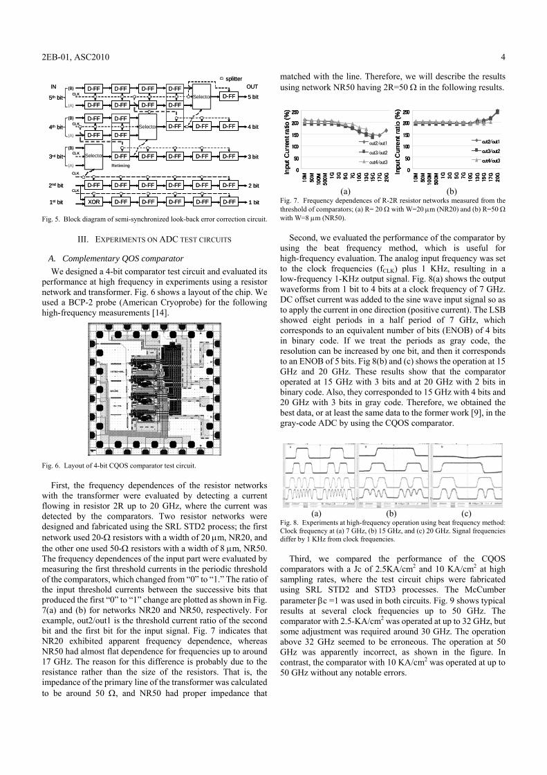
We also investigated a novel architecture in which the circuit was synchronized with a clock. Construction of fully synchronized circuits requires a large scale clock circuit and a complicated wiring layout for clock distribution with the same timing. Therefore, we conceived a semi-synchronized error correction circuit, as shown in Fig. 5. DFFs are used for clocked operation at every stage to avoid accumulating timing skew. Also, to avoid accumulating a timing difference between bits, the clock signals are sent to adjacent bits every once in a while, as shown in the figure.
OUT1bit
IN1A
IN3AIN2B
IN3B
OUT3bit
IN4A
IN4B
OUT4bit
IN5A
IN5B
OUT5bit
IN1A
IN3A
IN2B
IN3B
IN4A
IN4B
IN5A
IN5B
Analog input
Ioff_B- 3π/4 shift
Ioff_A- π/4 shift
Ioff_STD- π/2 shift
0 NegativePositive
OUT2bit
OUT1bit
IN1A
IN3AIN2B
IN3B
OUT3bit
IN4A
IN4B
OUT4bit
IN5A
IN5B
OUT5bit
IN1A
IN3A
IN2B
IN3B
IN4A
IN4B
IN5A
IN5B
Analog input
Ioff_B- 3π/4 shift
Ioff_A- π/4 shift
Ioff_STD- π/2 shift
0 NegativePositive
OUT2bit
2EB-01, ASC2010 4
Fig. 5. Block diagram of semi-synchronized look-back error correction circuit.
III. EXPERIMENTS ON ADC TEST CIRCUITS
A. Complementary QOS comparator We designed a 4-bit comparator test circuit and evaluated its
performance at high frequency in experiments using a resistor network and transformer. Fig. 6 shows a layout of the chip. We used a BCP-2 probe (American Cryoprobe) for the following high-frequency measurements [14].
Fig. 6. Layout of 4-bit CQOS comparator test circuit. First, the frequency dependences of the resistor networks
with the transformer were evaluated by detecting a current flowing in resistor 2R up to 20 GHz, where the current was detected by the comparators. Two resistor networks were designed and fabricated using the SRL STD2 process; the first network used 20-Ω resistors with a width of 20 μm, NR20, and the other one used 50-Ω resistors with a width of 8 μm, NR50. The frequency dependences of the input part were evaluated by measuring the first threshold currents in the periodic threshold of the comparators, which changed from “0” to “1.” The ratio of the input threshold currents between the successive bits that produced the first “0” to “1” change are plotted as shown in Fig. 7(a) and (b) for networks NR20 and NR50, respectively. For example, out2/out1 is the threshold current ratio of the second bit and the first bit for the input signal. Fig. 7 indicates that NR20 exhibited apparent frequency dependence, whereas NR50 had almost flat dependence for frequencies up to around 17 GHz. The reason for this difference is probably due to the resistance rather than the size of the resistors. That is, the impedance of the primary line of the transformer was calculated to be around 50 Ω, and NR50 had proper impedance that
matched with the line. Therefore, we will describe the results using network NR50 having 2R=50 Ω in the following results.
0
50
100
150
200
250
10M
50M
100M
500
M 1G
3G
5G 7G
10G
13G
15G
17G
20G
Inpu
t Cur
rent
ratio
(%)
out2/out1
out3/out2
out4/out3
0
50
100
150
200
250
10M
50M
100M
500M 1
G
3G
5G
7G
10G
13G
15G
17G
20G
out2/out1
out3/out2
out4/out3
Inpu
t Cur
rent
ratio
(%)
0
50
100
150
200
250
10M
50M
100M
500
M 1G
3G
5G 7G
10G
13G
15G
17G
20G
Inpu
t Cur
rent
ratio
(%)
out2/out1
out3/out2
out4/out3
0
50
100
150
200
250
10M
50M
100M
500
M 1G
3G
5G 7G
10G
13G
15G
17G
20G
Inpu
t Cur
rent
ratio
(%)
out2/out1
out3/out2
out4/out3
0
50
100
150
200
250
10M
50M
100M
500M 1
G
3G
5G
7G
10G
13G
15G
17G
20G
out2/out1
out3/out2
out4/out3
Inpu
t Cur
rent
ratio
(%)
0
50
100
150
200
250
10M
50M
100M
500M 1
G
3G
5G
7G
10G
13G
15G
17G
20G
out2/out1
out3/out2
out4/out3
out2/out1
out3/out2
out4/out3
Inpu
t Cur
rent
ratio
(%)
(a) (b)
Fig. 7. Frequency dependences of R-2R resistor networks measured from the threshold of comparators; (a) R= 20 Ω with W=20 μm (NR20) and (b) R=50 Ω with W=8 μm (NR50).
Second, we evaluated the performance of the comparator by
using the beat frequency method, which is useful for high-frequency evaluation. The analog input frequency was set to the clock frequencies (fCLK) plus 1 KHz, resulting in a low-frequency 1-KHz output signal. Fig. 8(a) shows the output waveforms from 1 bit to 4 bits at a clock frequency of 7 GHz. DC offset current was added to the sine wave input signal so as to apply the current in one direction (positive current). The LSB showed eight periods in a half period of 7 GHz, which corresponds to an equivalent number of bits (ENOB) of 4 bits in binary code. If we treat the periods as gray code, the resolution can be increased by one bit, and then it corresponds to an ENOB of 5 bits. Fig 8(b) and (c) shows the operation at 15 GHz and 20 GHz. These results show that the comparator operated at 15 GHz with 3 bits and at 20 GHz with 2 bits in binary code. Also, they corresponded to 15 GHz with 4 bits and 20 GHz with 3 bits in gray code. Therefore, we obtained the best data, or at least the same data to the former work [9], in the gray-code ADC by using the CQOS comparator.
(a) (b) (c)
Fig. 8. Experiments at high-frequency operation using beat frequency method: Clock frequency at (a) 7 GHz, (b) 15 GHz, and (c) 20 GHz. Signal frequencies differ by 1 KHz from clock frequencies.
Third, we compared the performance of the CQOS comparators with a Jc of 2.5KA/cm2 and 10 KA/cm2 at high sampling rates, where the test circuit chips were fabricated using SRL STD2 and STD3 processes. The McCumber parameter βc =1 was used in both circuits. Fig. 9 shows typical results at several clock frequencies up to 50 GHz. The comparator with 2.5-KA/cm2 was operated at up to 32 GHz, but some adjustment was required around 30 GHz. The operation above 32 GHz seemed to be erroneous. The operation at 50 GHz was apparently incorrect, as shown in the figure. In contrast, the comparator with 10 KA/cm2 was operated at up to 50 GHz without any notable errors.
D-FF
D-FF
D-FF
D-FF
D-FF
D-FF
D-FF
D-FF
D-FF
D-FF
D-FF
D-FF
D-FF
D-FF
D-FF
D-FF
D-FF
D-FF
D-FF
D-FF
D-FF
D-FF
D-FF
D-FF
D-FF
D-FF
D-FF
Selector
Selector
Selector
splitter
Retiming
(B)
(A)
(B)
(A)
(A)
(B)CLK
5 bit
4 bit
3 bit
2 bit
3rd bit
CLK
CLK
4th bit
5th bit
2nd bitCLK
OUTIN
D-FF D-FF D-FF D-FF D-FFXOR 1 bit1st bit
CLK
D-FF
D-FF
D-FF
D-FF
D-FF
D-FF
D-FF
D-FF
D-FF
D-FF
D-FF
D-FF
D-FF
D-FF
D-FF
D-FF
D-FF
D-FF
D-FF
D-FF
D-FF
D-FF
D-FF
D-FF
D-FF
D-FF
D-FF
Selector
Selector
Selector
splitter
Retiming
(B)
(A)
(B)
(A)
(A)
(B)CLK
5 bit
4 bit
3 bit
2 bit
3rd bit
CLK
CLK
4th bit
5th bit
2nd bitCLK
OUTIN
D-FF D-FF D-FF D-FF D-FFXOR 1 bit1st bit
CLK

2EB-01, ASC2010 5
50GHz45GHz
50GHz45GHz
(b)
(a)
20GHz
20GHz
Fig. 9. Operation of CQOS comparators fabricated using SRL Nb (a) STD2 (Jc= 2.5 KA/cm2) and (b) STD3 (Jc= 10 KA/cm2) processes at high-speed clock frequencies.
B. Integrated 5-bit ADCs We designed 5-bit binary ADCs in which the CQOS
comparators were integrated with error correction and interleaving circuits. The circuit was designed with OPEN cells in the CONNECT standard library except for the comparator and its peripheral circuits [15]. An RS-FF type SFQ/DC circuit, which was modified from the standard T-FF type SFQ/DC, was used in the outputs [11]. The resistor network NR20 was used in the present design. The IC chips were fabricated using SRL STD2 process.
Fig. 10(a) is a microphotograph of the first IC chip, in which the clock-flow type error correction circuit was adopted. The elemental circuits, such as comparators, DFFs, MUX, and variable delay JTLs, were locally allocated, and were connected by using passive transmission lines (PTLs). In this design, there were as many as 78 and 136 delay JTLs for the 4th and 5th bits. It is possible to replace them with other cell gates having a sufficiently large delay time.
OUT (5bit )
Analog Input
OUT (4bit )
OUT (3bit )
OUT (2bit )
OUT (1bit )
Retrieved waveform
-0.2
-0 .1 5
-0.1
-0 .0 5
0
0 .0 5
0.1
0 .1 5
0.2
0 1000 2000 3000 4000 5000 6000 7000 8000 9000 10000
0
0.05
0.1
0.15
0.2
0.25
0.3
0.35
0 1000 2000 3000 4000 5000 6000 7000 8000 9000 10000
0.15
0.2
0.25
0.3
0.35
0 1000 2000 3000 4000 5000 6000 7000 8000 9000 10000
0
0.05
0.1
0.15
0.2
0.25
0.3
0 1000 2000 3000 4000 5000 6000 7000 8000 9000 10000
0
0.05
0.1
0.15
0.2
0.25
0.3
0 1000 2000 3000 4000 5000 6000 7000 8000 9000 10000
0
0 .0 5
0.1
0 .1 5
0.2
0 .2 5
0.3
0 .3 5
0.4
0 1000 2000 3000 4000 5000 6000 7000 8000 9000 10000
-20
-15
-10
-5
0
5
10
15
20
0 1000 2000 3000 4000 5000 6000 7000 8000 9000 10000
(a) (b)
Fig. 10. (a) Microphotograph of an integrated ADC chip with error correction and interleaving circuits; (b) experimental results including the retrieved waveform.
A triangular analog input signal was applied to the ADC chip,
since comprehensible periodic output patterns can be expected. The circuit was tested at an input frequency of 100 Hz and a clock frequency of 100 KHz. We observed the operation with digital oscilloscopes, and the data were captured and processed off-line by a PC. Fig. 10(b) shows the input data and the digital
output from the 1st bit to the 5th bit. The 5th bit was used as a polarity bit in the experiment. Using these binary output data, we succeeded in reconstructing the triangular signal without any errors, as shown at the bottom of Fig. 10(b).
For this error-free operation, we needed to extract the ground current from several ground pads arranged around the chip. Fig. 11 shows the bias current and the extracting current to the pad on the chip. The total bias current was 436 mA, and the extracted current was 105 mA. When the same currents with the bias currents are extracted from the nearest ground pads, the circuit showed erroneous or incorrect operation. Also, the circuit did not work properly without any extracted currents.
Fig. 11. Bias current and extracting current for stable and error-free operation for the first ADC chip.
Next, a semi-synchronized ADC, shown in Fig. 12(a), was
designed and tested in a similar way to the first chip. In this scheme, the digital outputs, from the 1st bit to the 5th bit, were delayed by seven clocks because of the clocked operation. However, all of the output bits, from the 1st to the 5th, were output simultaneously because they were synchronized with the last clock signal input. Fig. 12(b) shows the input signal and 5-bit output digital signals. Since an analog input current twice as large as that in the experiment as shown in Fig. 10(b) was applied to the ADC, the 5th bit acted as a standard binary MSB, resulting in 5-bit ADC operation. The extracted currents were also required in this circuit; the total bias current was 314 mA and the extracted current was 147 mA.
(a) (b)
Fig. 12. (a) Layout of second integrated 5-bit ADC chip with semi-synchronized error correction circuit, and (b) experimentally observed correct outputs.

2EB-01, ASC2010 6
C. Experiments using cryocooling system Finally, we conducted some preliminary experiments using
our cryocooling systems with a 4K 1W GM cryocooler for future system-level development and experiments at high frequency. The ADC chips were flip-chip bonded on a multi-chip module (MCM) carrier made with a silicon substrate [16] -[18]. The chip and MCM carrier measured 5 x 5 mm and 16 x 16 mm. The flip-chip bonding pad was 50 μm in diameter. We have developed a new module-type MCM package with a bandwidth of more than 40 GHz in place of the cryoprobe structure. The MCM package enables us to set and change the MCM substrates more easily. Also, the modules (packages) can be easily changed with an eight-terminal miniature coaxial connector, which was also developed for the MCM package. The package has 32 terminals in total, and 4 sets of connectors were attached to the package. Fig 13(a) shows a photograph of the 4 K stage of our cooling system, in which the MCM package with ADC chip is assembled. Fig. 13(b) shows a photograph of the setup of the system-level experiments using the cryocooling system. The ADC chips were cooled to around 4 K, and we successfully confirmed that they operated normally, just as they did in liquid-helium cooling. No special differences or heating problems were observed in the experiments.
(a) (b)
Fig. 13. (a) Photograph of 4K stage in our cooling system, where new module type MCM package and coaxial connectors were introduced, and (b) setup used to measure ADCs with a cryocooling system.
IV. CONCLUSION We have designed and tested 5-bit flash-type SFQ ADCs,
which had CQOS comparators integrated with error correction and bit-interleaving circuits. Two look-back error correction circuits were integrated into the ADC ICs. We confirmed that both of the ADCs carried out error correction at low frequency. Besides laboratory-level experiments cooled with liquid helium, we confirmed that the ADCs operated successfully as a preliminary system-level implementation using a cryocooling system with a 4K GM cryocooler. In addition, the high-frequency characteristics of the CQOS comparator and its input circuit, an R-2R resistor network and a transformer, were investigated toward future high-frequency operation of the integrated ADCs. We confirmed 3-bit binary operation at 15 GHz and 4-bit gray operation at 15 GHz using the beat frequency method in a 4-bit comparator test circuit. Also, we were able to observe high-speed sampling operations at up to 32 GHz with a Jc of 2.5 KA/cm2 and at up to 50 GHz with a Jc of 10 KA/cm2.
ACKNOWLEDGMENT The authors would like to thank Ms. M. Isaka and the
members of ISTEC-SRL for fabricating the IC chips, and Ms. M. Katsume for assembling the MCMs. The National Institute of Advanced Industrial Science and Technology partially contributed to the circuit fabrication. We also express our gratitude to S. Akasaka of Kawashima Manufacturing Co, Ltd. for developing the MCM package and connector.
REFERENCES [1] K. K. Likharev and V. K. Semenov, “RSFQ logic/memory family: A new
Josephson-junction technology for sub-terahertz-clock frequency digital systems,” IEEE Trans.Appl. Superconductivity, vol. 1, no. 1, pp. 3–28, Mar. 1991.
[2] H. H. Zappe, “Ultrasensitive analog to digital converter using Josephson junctions,” IBM Tech. Disc. Bull., vol. 17, pp. 3053-3054, Mar. 1975..
[3] R. E. Harris, C. A. Hamilton, and F. L. Lloyd, “Multiple-quantum interference superconducting analog-to-digital converter,” Appl. Phys. Lett., vol. 35, pp. 720-721, 1979.
[4] H. Ko and T. Van Duzer, “A new high-speed periodic-threshold comparator for use in a Josephson A/D converter,” IEEE J. Solid-State Circuits, vol. 23, pp. 1017-1021, Aug. 1988.
[5] H. Ko, “A flash Josephson A/D converter constructed with one-junction SQUIDs,” IEEE Trans. Magn., vol. 25, Mar. 1989.
[6] O. A. Mukhanov, D. Gupta, A. M. Kadin, and V. K. Semenov, “Superconductor analog-to-digital converters,” Proc. IEEE, vol. 92, pp. 1564-1584, Oct. 2004.
[7] P. D. Bradley and S. V. Rylov, “A comparison of two types of single flux quantum comparators for a flash ADC with 10 GHz input bandwidth,” IEEE Trans. Appl. Supercond., vol. 7, pp. 2677-2680, Jun. 1997.
[8] S. B. Kaplan, S. V. Rylov, and P. D. Bradley, “Real-time digital error correction for flash analog-to-digital converter,” IEEE Trans. Appl. Supercond., vol. 7, pp. 2822-2825, Jun. 1997.
[9] S. B. Kaplan, P. D. Bradley, D. K. Brock, D. Gaidarenko, D. Gupta, W.Q. Li, and S. V. Rylov, “A superconductive flash digitizer with on-chip memory,” IEEE Trans. Appl. Supercond., vol. 9, pp. 3020-3025, Jun. 1999.
[10] H. Suzuki, M. Maruyama, Y. Hashimoto, K. Fujiwara, and M. Hidaka, “Possible application of flash-type SFQ A/D converter to optical communication systems and their measuring instruments,”, IEEE Trans. Appl. Supercon.. vol. 19, pp. 611-616, Jun. 2009.
[11] M. Maruyama, H. Suzuki, Y. Hashimoto, and M. Hidaka, “A flash A/D converter using complementarily combined SQUIDs,”, IEEE Trans. Appl. Supercon.. vol. 19, pp. 680-684, Jun. 2009.
[12] Microwave office, AWR corporation, http://web.awrcorp.com. [13] H. Barker, “A transducer for digital data-transition systems,” Proc. IEEE,
vol. 103B, pp. 42-51, 1956. [14] American cryoprobe, Fall city, WA 98024-1262, e-mail :
[email protected].. [15] S. Yorozu, Y. Kameda, H. Terai, A. Fujimaki, T. Yamada, and S. Tahar,
“A single flux quantum standard cell library,” Physica C, vol. 372-376, pp. 1471-1474, 2002.
[16] Y. Hshimoto, S. Yorozu, T. Satoh, and T. Miyazaki, “Demonstration of chip-to-chip transmission of single-flux-quantum pulses at throughputs beyond 100 Gbps, ” Appl. Phys. Lett., 2005, 022502.
[17] Y. Hashimoto, S. Yorozu, T. Miyazaki, Y. Kameda, H. Suzuki, and N. Yoshikawa, “Implementation and experimental evaluation of a cryocooled system prototype for high-throughput SFQ digital applications,” IEEE Trans.Appl. Superconductivity, vol. 17, no. 2, pp. 546–551, Jun. 2007.
[18] Y. Hashimoto, S. Yorozu, and Y. Kameda, “Development of cryopackaging and I/O technologies for high-speed superconductive digital systems,” IEiC TransElectron., vol. E91-C, no. 3, pp. 325–332, March 2008.


