Embed Size (px)
Citation preview
Power Integrations 5245 Hellyer Avenue, San Jose, CA 95138 USA. Tel: +1 408 414 9200 Fax: +1 408 414 9201
www.power.com
Design Example Report
Title Dual Output 17.5 W Power Supply Using InnoSw itchTM-EP INN2904K
Specification 85 VAC – 484 VAC Input; 12 V, 1.25 A and 5 V, 0.5 A Outputs
Application Embedded Power Supply
Author Applications Engineering Department
Document Number DER-531
Date July 12, 2016
Revision 1.2
Summary and Features • InnoSwitch-EP - industry first AC/DC ICs with isolated, safety rated integrated feedback
• 900 V rated MOSFET• Built in synchronous rectification for higher efficiency• All the benefits of secondary side control with the simplicity of primary side regulation
• Insensitive to transformer variation• Extremely fast transient response independent of load timing
• Meets output cross regulation requirements without linear regulators• Primary sensed output overvoltage protection (OVP) eliminates optocoupler for fault
protection• Accurate thermal protection with hysteretic shutdown• Input voltage monitor with accurate brown-in/brown-out and overvoltage protection
PATENT INFORMATION The products and applications illustrated herein (including transformer construction and circuits external to the products) may be covered by one or more U.S. and foreign patents, or potentially by pending U.S. and foreign patent applications assigned to Power Integrations. A complete list of Power Integrations' patents may be found at www.powerint.com. Power Integrations grants its customers a license under certain patent rights as set forth at <http://www.powerint.com/ip.htm>.
DER-531 17.5 W InnoSwitch-EP Dual Output Supply 12-Jul-16
Page 2 of 42
Power Integrations, Inc. Tel: +1 408 414 9200 Fax: +1 408 414 9201 www.power.com
Table of Contents 1 Introduction ......................................................................................................... 4 2 Power Supply Specification ................................................................................... 5 3 Schematic ............................................................................................................ 6 4 Circuit Description ................................................................................................ 7
Input EMI Filtering ......................................................................................... 7 4.1 InnoSwitch-EP Primary ................................................................................... 7 4.2 InnoSwitch-EP Secondary ............................................................................... 7 4.3
5 PCB Layout .......................................................................................................... 9 6 Bill of Materials .................................................................................................. 10 7 Transformer (T1) Specification ............................................................................ 11
Transformer Electrical Diagram ..................................................................... 11 7.1 Electrical Specifications ................................................................................ 11 7.2 Material List ................................................................................................ 11 7.3 Transformer Build Diagram .......................................................................... 12 7.4
8 Common Mode Choke (L1) Specification .............................................................. 13 Electrical Diagram ........................................................................................ 13 8.1 Electrical Specifications ................................................................................ 13 8.2 Material List ................................................................................................ 13 8.3 Winding Instructions .................................................................................... 13 8.4 Illustrations ................................................................................................. 13 8.5
9 Transformer Design Spreadsheet ........................................................................ 14 10 Performance Data ........................................................................................... 18
Full Load Efficiency vs. Line .......................................................................... 18 10.1 No-Load Input Power ................................................................................... 19 10.2 Line and Load Regulation ............................................................................. 20 10.3
10.3.1 Line Regulation (Full Load) .................................................................... 20 10.3.2 Cross Load Regulation ........................................................................... 21
11 Thermal Performance ...................................................................................... 24 85 VAC........................................................................................................ 24 11.1 484 VAC ...................................................................................................... 25 11.2
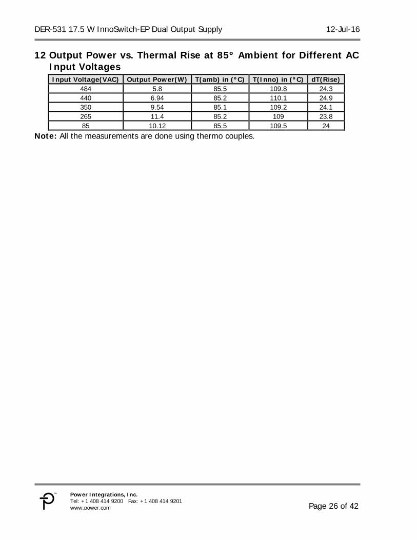
12 Output Power vs. Thermal Rise at 85º Ambient for Different AC Input Voltages .. 26 13 Waveforms ..................................................................................................... 27
Load Transient Response ............................................................................. 27 13.113.1.1 5 V Load Transient (No-Load to Full Load) and No-Load on 12 V Output .. 27 13.1.2 5 V Load Transient (No-Load to Full Load) and Full Load on 12 V Output . 28 13.1.3 12 V Load Transient (No-Load to Full Load) and No-Load on 5 V Output .. 28 13.1.4 12 V Load Transient (No-Load to Full Load) and Full Load on 5 V Output . 29
Switching Waveforms ................................................................................... 30 13.213.2.1 InnoSwitch-EP Waveforms ..................................................................... 30 13.2.2 SR FET Waveforms ............................................................................... 31 13.2.3 Output Voltage and Current Waveforms During Start-Up ......................... 32
Output Ripple Measurements ........................................................................ 33 13.3
12-Jul-16 DER-531 17.5 W InnoSwitch-EP Dual Output Supply
Page 3 of 42
Power Integrations Tel: +1 408 414 9200 Fax: +1 408 414 9201
www.power.com
13.3.1 Ripple Measurement Technique ............................................................. 33 13.3.2 Ripple Voltage Waveforms ..................................................................... 34
Line Undervoltage and Overvoltage (DC Input) .............................................. 35 13.414 ESD................................................................................................................ 36 15 EMI ................................................................................................................ 36
Conductive EMI ........................................................................................... 36 15.115.1.1 Earth Grounded Output (QP / AV) .......................................................... 36
16 Lighting Surge Test ......................................................................................... 40 Combination Wave Differential Mode Test ..................................................... 40 16.1 Ring Wave Common Mode Test .................................................................... 40 16.2
17 Revision History .............................................................................................. 41 Important Note: Although this board is designed to satisfy safety isolation requirements, the engineering prototype has not been agency approved. Therefore, all testing should be performed using an isolation transformer to provide the AC input to the prototype board.
DER-531 17.5 W InnoSwitch-EP Dual Output Supply 12-Jul-16
Page 4 of 42
Power Integrations, Inc. Tel: +1 408 414 9200 Fax: +1 408 414 9201 www.power.com
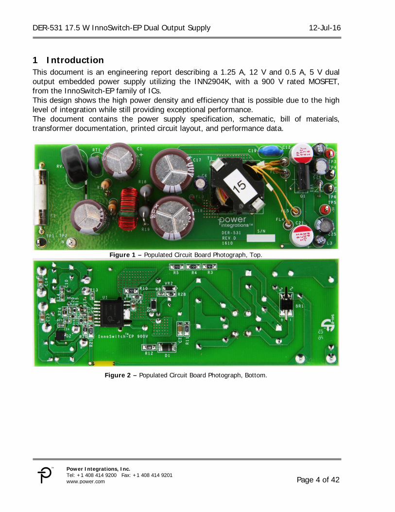
1 Introduction This document is an engineering report describing a 1.25 A, 12 V and 0.5 A, 5 V dual output embedded power supply utilizing the INN2904K, with a 900 V rated MOSFET, from the InnoSwitch-EP family of ICs. This design shows the high power density and efficiency that is possible due to the high level of integration while still providing exceptional performance. The document contains the power supply specification, schematic, bill of materials, transformer documentation, printed circuit layout, and performance data.
Figure 1 – Populated Circuit Board Photograph, Top.
Figure 2 – Populated Circuit Board Photograph, Bottom.
12-Jul-16 DER-531 17.5 W InnoSwitch-EP Dual Output Supply
Page 5 of 42
Power Integrations Tel: +1 408 414 9200 Fax: +1 408 414 9201
www.power.com
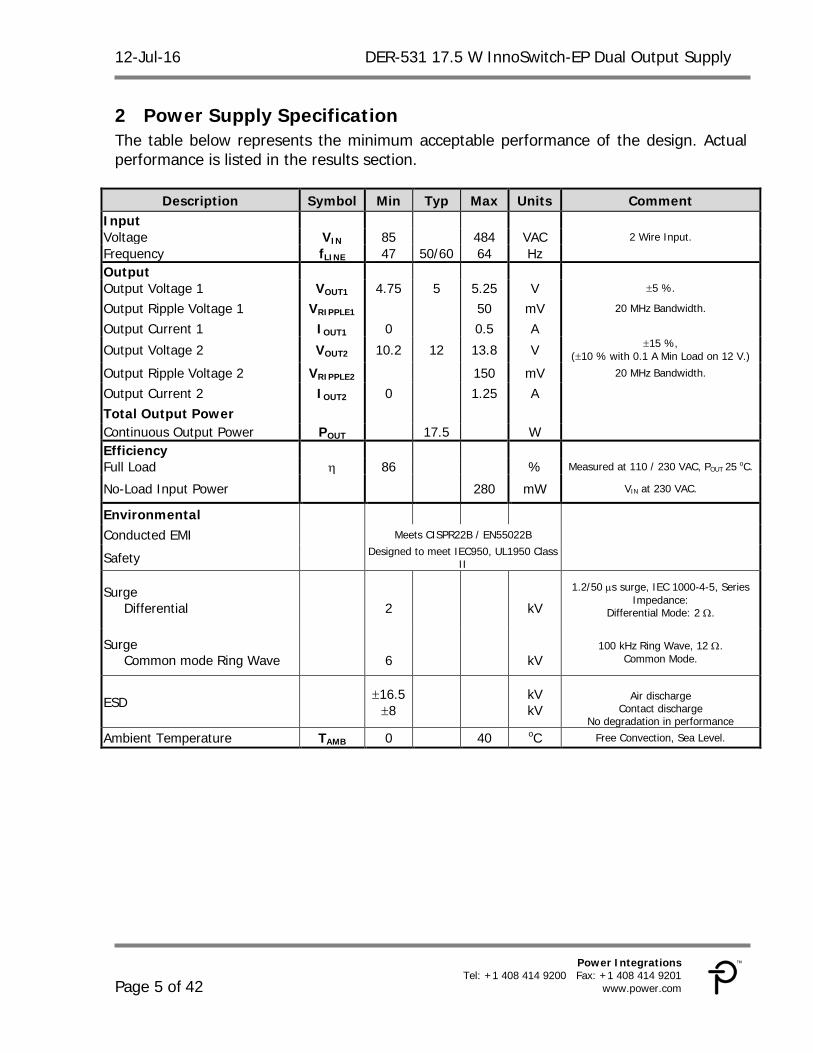
2 Power Supply Specification The table below represents the minimum acceptable performance of the design. Actual performance is listed in the results section.
Description Symbol Min Typ Max Units Comment Input Voltage VIN 85 484 VAC 2 Wire Input.
Frequency fLINE 47 50/60 64 Hz
Output
Output Voltage 1 VOUT1 4.75 5 5.25 V ±5 %.
Output Ripple Voltage 1 VRIPPLE1 50 mV 20 MHz Bandwidth.
Output Current 1 IOUT1 0 0.5 A
Output Voltage 2 VOUT2 10.2 12 13.8 V ±15 %, (±10 % with 0.1 A Min Load on 12 V.)
Output Ripple Voltage 2 VRIPPLE2 150 mV 20 MHz Bandwidth.
Output Current 2 IOUT2 0 1.25 A
Total Output Power
Continuous Output Power POUT 17.5 W
Efficiency
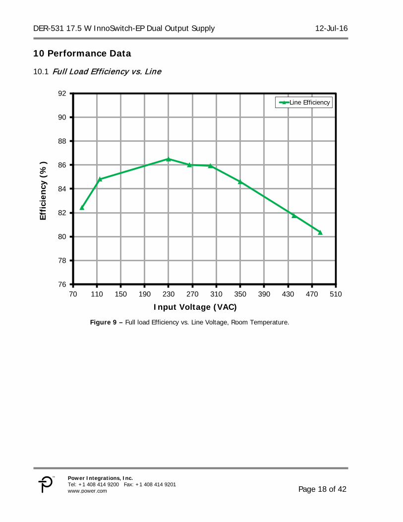
Full Load η 86 % Measured at 110 / 230 VAC, POUT 25 oC.
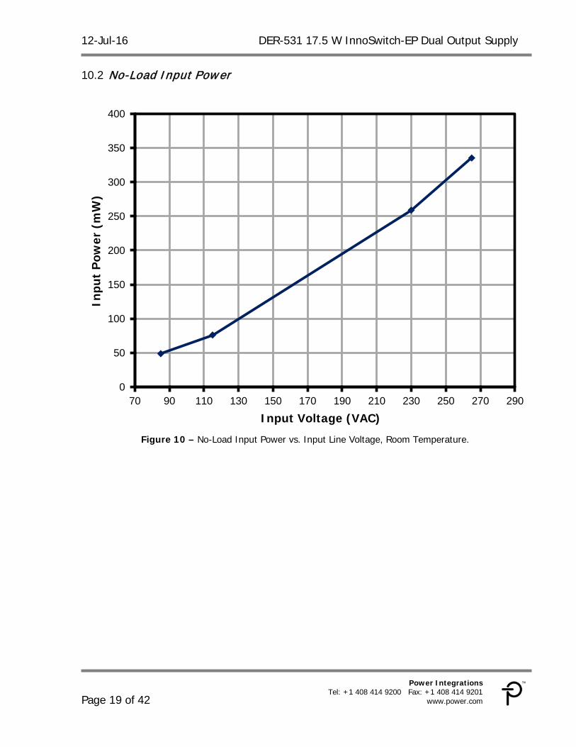
No-Load Input Power 280 mW VIN at 230 VAC.
Environmental
Conducted EMI Meets CISPR22B / EN55022B
Safety Designed to meet IEC950, UL1950 Class II
Surge Differential
2 kV
1.2/50 µs surge, IEC 1000-4-5, Series Impedance:
Differential Mode: 2 Ω.
Surge Common mode Ring Wave
6 kV
100 kHz Ring Wave, 12 Ω. Common Mode.
ESD ±16.5 ±8 kV
kV
Air discharge
Contact discharge No degradation in performance
Ambient Temperature TAMB 0 40 oC Free Convection, Sea Level.
DER-531 17.5 W InnoSwitch-EP Dual Output Supply 12-Jul-16
Page 6 of 42
Power Integrations, Inc. Tel: +1 408 414 9200 Fax: +1 408 414 9201 www.power.com
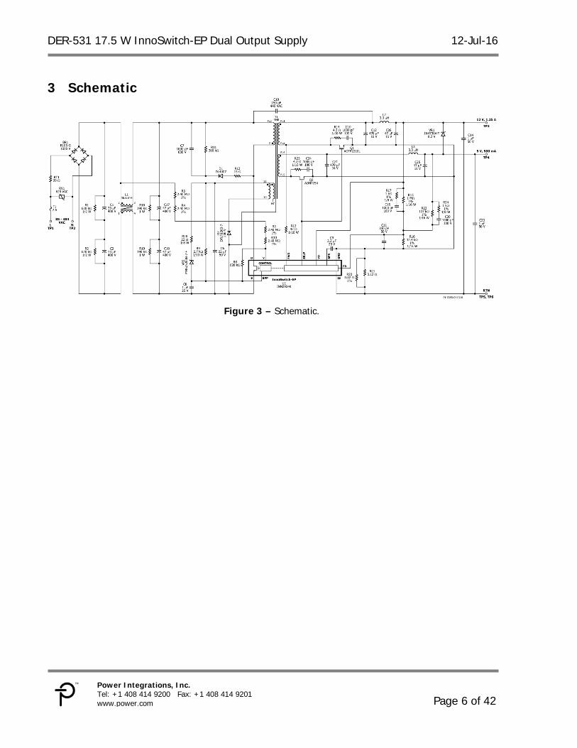
3 Schematic
Figure 3 – Schematic.
12-Jul-16 DER-531 17.5 W InnoSwitch-EP Dual Output Supply
Page 7 of 42
Power Integrations Tel: +1 408 414 9200 Fax: +1 408 414 9201
www.power.com
4 Circuit Description
Input EMI Filtering 4.1Fuse F1 isolates the circuit and provides protection from component failure and the common mode chokes L1 with capacitors, C1, C2, C17 and C18, provides attenuation for EMI. Bridge rectifier BR1 rectifies the AC line voltage and provides a full wave rectified DC across the filter consisting of C1 and C2. Thermistor RT1 is an inrush current limiter in the circuit with the high peak forward surge current rated bridge rectifier.
InnoSw itch-EP Primary 4.2One side of the transformer primary is connected to the rectified DC bus, the other is connected to the integrated 900 V power MOSFET inside the InnoSwitch-EP IC (U1). A low cost RCD clamp formed by D1, R11, R12, and C7 limits the peak drain voltage due to the effects of transformer leakage reactance and output trace inductance. The IC is self-starting, using an internal high-voltage current source to charge the BPP pin capacitor, C8, when AC is first applied. During normal operation the primary side block is powered from an auxiliary winding on the transformer. The output of this is configured as a flyback winding which is rectified and filtered using diode D2 and capacitor C6, and fed in the BPP pin via a current limiting resistor R9. The primary side overvoltage protection is obtained using Zener diode VR2 and R28. In the event of overvoltage at output, the increased voltage at the output of the bias winding cause the Zener diode VR2 to conduct and triggers the OVP latch in the primary side controller of the InnoSwitch-EP IC. Resistor R3, R4, R5, R10 and R8 provide line voltage sensing and provide a current to U1, which is proportional to the DC voltage across capacitors C1 and C2. At approximately 78 V DC, the current through these resistors exceeds the line under-voltage threshold, which results in enabling of U1. At approximately 700 V DC, the current through these resistors exceeds the line over-voltage threshold, which results in disabling of U1.
InnoSw itch-EP Secondary 4.3The secondary side of the InnoSwitch-EP provides output voltage, output current sensing and drive to a MOSFET providing synchronous rectification. Output rectification for the 5 V output is provided by SR FET Q2. Very low ESR capacitor C21 provides filtering, and inductor L3 and capacitor C25 form a second stage filter that significantly attenuates the high frequency ripple and noise at the 5 V output. Output rectification for the 12 V output is provided by SR FET Q1. Very low ESR capacitors C12 provides filtering, and inductor L2 and capacitor C26 form a second stage
DER-531 17.5 W InnoSwitch-EP Dual Output Supply 12-Jul-16
Page 8 of 42
Power Integrations, Inc. Tel: +1 408 414 9200 Fax: +1 408 414 9201 www.power.com
filter that significantly attenuates the high frequency ripple and noise at the 12 V output. C14 and C23 capacitors are used to high frequency switching ripple and radiated EMI. RC snubber networks comprising R25 and C24 for Q2, R14 and C10 for Q1 damp high frequency ringing across SR FETs, which results from leakage inductance of the transformer windings and the secondary trace inductances. In continuous conduction mode operation, the power MOSFET is turned off just prior to the secondary side controller commanding a new switching cycle from the primary. In discontinuous mode the MOSFET is turned off when the voltage drop across the MOSFET falls below a threshold (VSR(TH)). Secondary side control of the primary side MOSFET ensure that it is never on simultaneously with the synchronous rectification MOSFET. The MOSFET drive signal is output on the SR/P pin. The secondary side of the IC is self-powered from either the secondary winding forward voltage or the output voltage. The output voltage powers the device, fed into the VO pin and charges the decoupling capacitor C9 via an internal regulator during CV region and forward secondary winding forward voltage powers the device during startup and CC region through R13. The unit enters auto-restart when the sensed output voltage is lower than 3 V. Resistor R16, R15 and R23 form a voltage divider network that senses the output voltage from both outputs for better cross-regulation. Zener diode VR1 improves the cross regulation when only the 5 V output is loaded, which results in the 12 V output operating at the higher end of the specification. The InnoSwitch-EP IC has an internal reference of 1.265 V. Feedback compensation networks comprising capacitors C20, C15 and resistors R24, R17 reduce the output ripple voltage. Capacitor C11 provides decoupling from high frequency noise affecting power supply operation. Total output current is sensed by R20 and R21 with a threshold of approximately 33 mV to reduce losses. Once the current sense threshold across these resistors is exceeded, the device adjusts the number of switch pulses to maintain a fixed output current
12-Jul-16 DER-531 17.5 W InnoSwitch-EP Dual Output Supply
Page 9 of 42
Power Integrations Tel: +1 408 414 9200 Fax: +1 408 414 9201
www.power.com
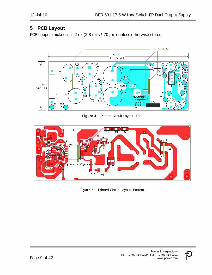
5 PCB Layout PCB copper thickness is 2 oz (2.8 mils / 70 µm) unless otherwise stated.
Figure 4 – Printed Circuit Layout, Top.
Figure 5 – Printed Circuit Layout, Bottom.
DER-531 17.5 W InnoSwitch-EP Dual Output Supply 12-Jul-16
Page 10 of 42
Power Integrations, Inc. Tel: +1 408 414 9200 Fax: +1 408 414 9201 www.power.com
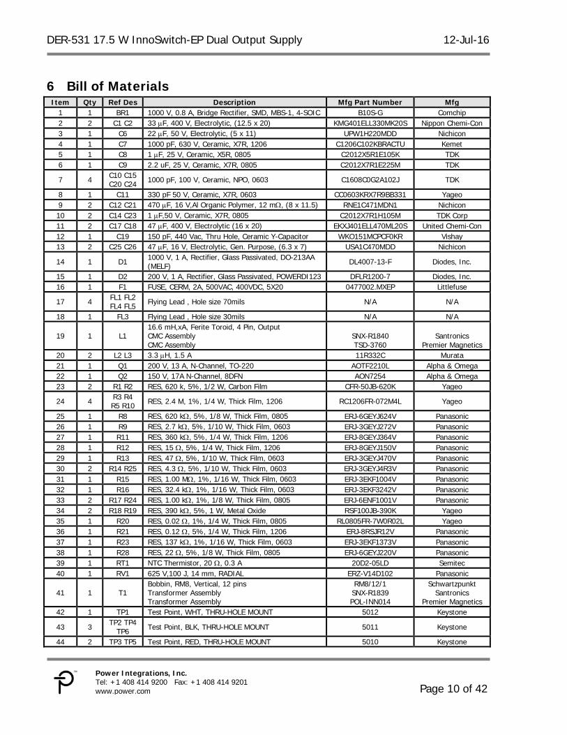
6 Bill of Materials Item Qty Ref Des Description Mfg Part Number Mfg
1 1 BR1 1000 V, 0.8 A, Bridge Rectifier, SMD, MBS-1, 4-SOIC B10S-G Comchip 2 2 C1 C2 33 µF, 400 V, Electrolytic, (12.5 x 20) KMG401ELL330MK20S Nippon Chemi-Con 3 1 C6 22 µF, 50 V, Electrolytic, (5 x 11) UPW1H220MDD Nichicon 4 1 C7 1000 pF, 630 V, Ceramic, X7R, 1206 C1206C102KBRACTU Kemet 5 1 C8 1 µF, 25 V, Ceramic, X5R, 0805 C2012X5R1E105K TDK 6 1 C9 2.2 uF, 25 V, Ceramic, X7R, 0805 C2012X7R1E225M TDK
7 4 C10 C15 C20 C24 1000 pF, 100 V, Ceramic, NPO, 0603 C1608C0G2A102J TDK
8 1 C11 330 pF 50 V, Ceramic, X7R, 0603 CC0603KRX7R9BB331 Yageo 9 2 C12 C21 470 µF, 16 V,Al Organic Polymer, 12 mΩ, (8 x 11.5) RNE1C471MDN1 Nichicon 10 2 C14 C23 1 µF,50 V, Ceramic, X7R, 0805 C2012X7R1H105M TDK Corp 11 2 C17 C18 47 µF, 400 V, Electrolytic (16 x 20) EKXJ401ELL470ML20S United Chemi-Con 12 1 C19 150 pF, 440 Vac, Thru Hole, Ceramic Y-Capacitor WKO151MCPCF0KR Vishay 13 2 C25 C26 47 µF, 16 V, Electrolytic, Gen. Purpose, (6.3 x 7) USA1C470MDD Nichicon
14 1 D1 1000 V, 1 A, Rectifier, Glass Passivated, DO-213AA (MELF) DL4007-13-F Diodes, Inc.
15 1 D2 200 V, 1 A, Rectifier, Glass Passivated, POWERDI123 DFLR1200-7 Diodes, Inc. 16 1 F1 FUSE, CERM, 2A, 500VAC, 400VDC, 5X20 0477002.MXEP Littlefuse
17 4 FL1 FL2 FL4 FL5 Flying Lead , Hole size 70mils N/A N/A
18 1 FL3 Flying Lead , Hole size 30mils N/A N/A
19 1 L1 16.6 mH,xA, Ferite Toroid, 4 Pin, Output CMC Assembly CMC Assembly
SNX-R1840 TSD-3760
Santronics
Premier Magnetics 20 2 L2 L3 3.3 µH, 1.5 A 11R332C Murata 21 1 Q1 200 V, 13 A, N-Channel, TO-220 AOTF2210L Alpha & Omega 22 1 Q2 150 V, 17A N-Channel, 8DFN AON7254 Alpha & Omega 23 2 R1 R2 RES, 620 k, 5%, 1/2 W, Carbon Film CFR-50JB-620K Yageo
24 4 R3 R4 R5 R10 RES, 2.4 M, 1%, 1/4 W, Thick Film, 1206 RC1206FR-072M4L Yageo
25 1 R8 RES, 620 kΩ, 5%, 1/8 W, Thick Film, 0805 ERJ-6GEYJ624V Panasonic 26 1 R9 RES, 2.7 kΩ, 5%, 1/10 W, Thick Film, 0603 ERJ-3GEYJ272V Panasonic 27 1 R11 RES, 360 kΩ, 5%, 1/4 W, Thick Film, 1206 ERJ-8GEYJ364V Panasonic 28 1 R12 RES, 15 Ω, 5%, 1/4 W, Thick Film, 1206 ERJ-8GEYJ150V Panasonic 29 1 R13 RES, 47 Ω, 5%, 1/10 W, Thick Film, 0603 ERJ-3GEYJ470V Panasonic 30 2 R14 R25 RES, 4.3 Ω, 5%, 1/10 W, Thick Film, 0603 ERJ-3GEYJ4R3V Panasonic 31 1 R15 RES, 1.00 MΩ, 1%, 1/16 W, Thick Film, 0603 ERJ-3EKF1004V Panasonic 32 1 R16 RES, 32.4 kΩ, 1%, 1/16 W, Thick Film, 0603 ERJ-3EKF3242V Panasonic 33 2 R17 R24 RES, 1.00 kΩ, 1%, 1/8 W, Thick Film, 0805 ERJ-6ENF1001V Panasonic 34 2 R18 R19 RES, 390 kΩ, 5%, 1 W, Metal Oxide RSF100JB-390K Yageo 35 1 R20 RES, 0.02 Ω, 1%, 1/4 W, Thick Film, 0805 RL0805FR-7W0R02L Yageo 36 1 R21 RES, 0.12 Ω, 5%, 1/4 W, Thick Film, 1206 ERJ-8RSJR12V Panasonic 37 1 R23 RES, 137 kΩ, 1%, 1/16 W, Thick Film, 0603 ERJ-3EKF1373V Panasonic 38 1 R28 RES, 22 Ω, 5%, 1/8 W, Thick Film, 0805 ERJ-6GEYJ220V Panasonic 39 1 RT1 NTC Thermistor, 20 Ω, 0.3 A 20D2-05LD Semitec 40 1 RV1 625 V,100 J, 14 mm, RADIAL ERZ-V14D102 Panasonic
41 1 T1 Bobbin, RM8, Vertical, 12 pins Transformer Assembly Transformer Assembly
RM8/12/1 SNX-R1839 POL-INN014
Schwartzpunkt Santronics
Premier Magnetics 42 1 TP1 Test Point, WHT, THRU-HOLE MOUNT 5012 Keystone
43 3 TP2 TP4 TP6 Test Point, BLK, THRU-HOLE MOUNT 5011 Keystone
44 2 TP3 TP5 Test Point, RED, THRU-HOLE MOUNT 5010 Keystone
12-Jul-16 DER-531 17.5 W InnoSwitch-EP Dual Output Supply
Page 11 of 42
Power Integrations Tel: +1 408 414 9200 Fax: +1 408 414 9201
www.power.com
45 1 U1 InnoSwitch-EP, Off-Line CV/CC Flyback Switcher INN2904K Power Integrations 46 1 VR1 8.2 V, 5%, 1 W, DO-41 1N4738A,113 NXP Semi 47 1 VR2 DIODE ZENER 4.7V 500MW SOD123 MMSZ5230B-7-F Diodes, Inc.
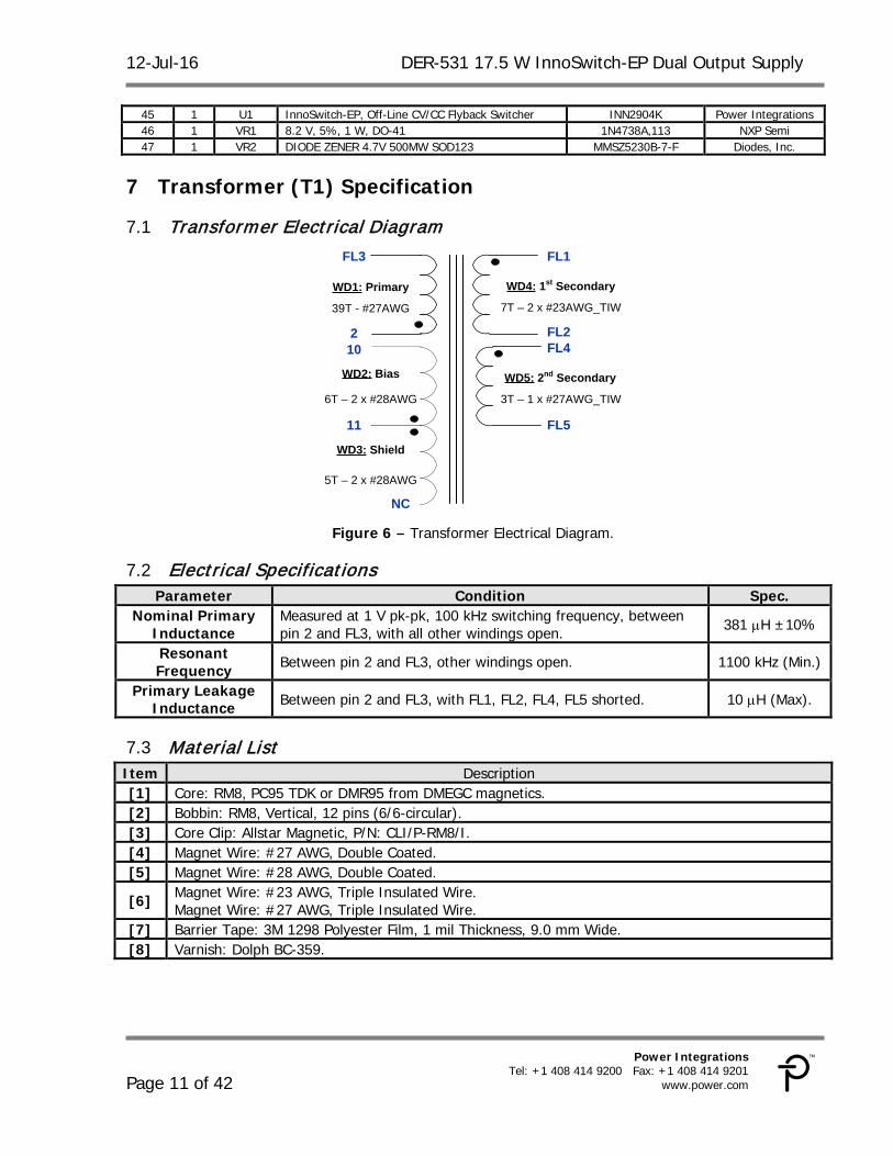
7 Transformer (T1) Specification
Transformer Electrical Diagram 7.1
Figure 6 – Transformer Electrical Diagram.
Electrical Specifications 7.2Parameter Condition Spec.
Nominal Primary Inductance
Measured at 1 V pk-pk, 100 kHz switching frequency, between pin 2 and FL3, with all other windings open. 381 µH ±10%
Resonant Frequency Between pin 2 and FL3, other windings open. 1100 kHz (Min.)
Primary Leakage Inductance Between pin 2 and FL3, with FL1, FL2, FL4, FL5 shorted. 10 µH (Max).
Material List 7.3Item Description [1] Core: RM8, PC95 TDK or DMR95 from DMEGC magnetics. [2] Bobbin: RM8, Vertical, 12 pins (6/6-circular). [3] Core Clip: Allstar Magnetic, P/N: CLI/P-RM8/I. [4] Magnet Wire: #27 AWG, Double Coated. [5] Magnet Wire: #28 AWG, Double Coated.
[6] Magnet Wire: #23 AWG, Triple Insulated Wire. Magnet Wire: #27 AWG, Triple Insulated Wire.
[7] Barrier Tape: 3M 1298 Polyester Film, 1 mil Thickness, 9.0 mm Wide. [8] Varnish: Dolph BC-359.
2
FL3
11
10
NC
FL1
FL2FL4
FL5
WD1: Primary
WD2: Bias
WD3: Shield
WD5: 2nd Secondary
WD4: 1st Secondary
39T - #27AWG
6T – 2 x #28AWG
5T – 2 x #28AWG
7T – 2 x #23AWG_TIW
3T – 1 x #27AWG_TIW

DER-531 17.5 W InnoSwitch-EP Dual Output Supply 12-Jul-16
Page 12 of 42
Power Integrations, Inc. Tel: +1 408 414 9200 Fax: +1 408 414 9201 www.power.com
Transformer Build Diagram 7.4
2
FL3
11
10 NC
FL1FL2
FL4FL5
WD1: Primary
WD2: Bias
WD3: Shield
WD4: 1st Secondary
WD5: 2nd Secondary
39T - #27AWG
6T – 2 x #28AWG
5T – 2 x #28AWG
7T – 2 x #23AWG_TIW
3T – 1 x #27AWG_TIW
(wound in parallel with…)
Figure 7 – Transformer Build Diagram.
12-Jul-16 DER-531 17.5 W InnoSwitch-EP Dual Output Supply
Page 13 of 42
Power Integrations Tel: +1 408 414 9200 Fax: +1 408 414 9201
www.power.com
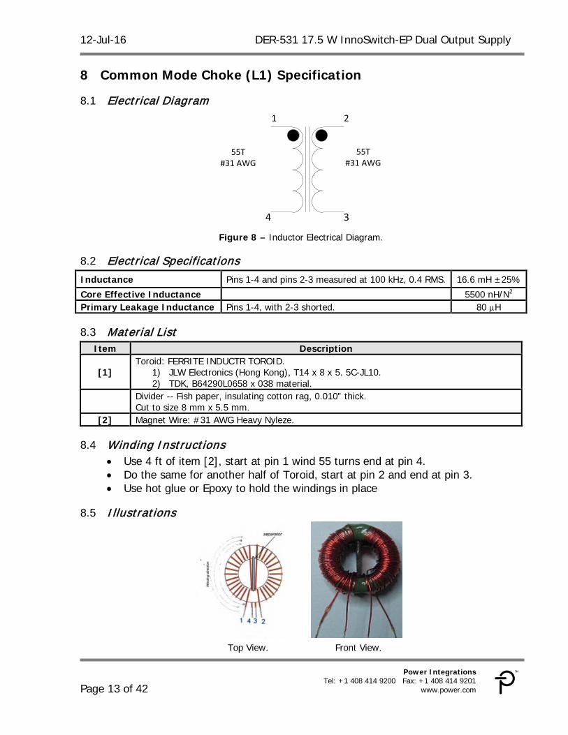
8 Common Mode Choke (L1) Specification
Electrical Diagram 8.1
Figure 8 – Inductor Electrical Diagram.
Electrical Specifications 8.2
Inductance Pins 1-4 and pins 2-3 measured at 100 kHz, 0.4 RMS. 16.6 mH ±25%
Core Effective Inductance 5500 nH/N2
Primary Leakage Inductance Pins 1-4, with 2-3 shorted. 80 µH
Material List 8.3Item Description
[1] Toroid: FERRITE INDUCTR TOROID.
1) JLW Electronics (Hong Kong), T14 x 8 x 5. 5C-JL10. 2) TDK, B64290L0658 x 038 material.
Divider -- Fish paper, insulating cotton rag, 0.010” thick. Cut to size 8 mm x 5.5 mm.
[2] Magnet Wire: #31 AWG Heavy Nyleze.
Winding Instructions 8.4• Use 4 ft of item [2], start at pin 1 wind 55 turns end at pin 4. • Do the same for another half of Toroid, start at pin 2 and end at pin 3. • Use hot glue or Epoxy to hold the windings in place
I llustrations 8.5
Top View. Front View.
4
1
3
2
55T#31 AWG
55T#31 AWG
DER-531 17.5 W InnoSwitch-EP Dual Output Supply 12-Jul-16
Page 14 of 42
Power Integrations, Inc. Tel: +1 408 414 9200 Fax: +1 408 414 9201 www.power.com
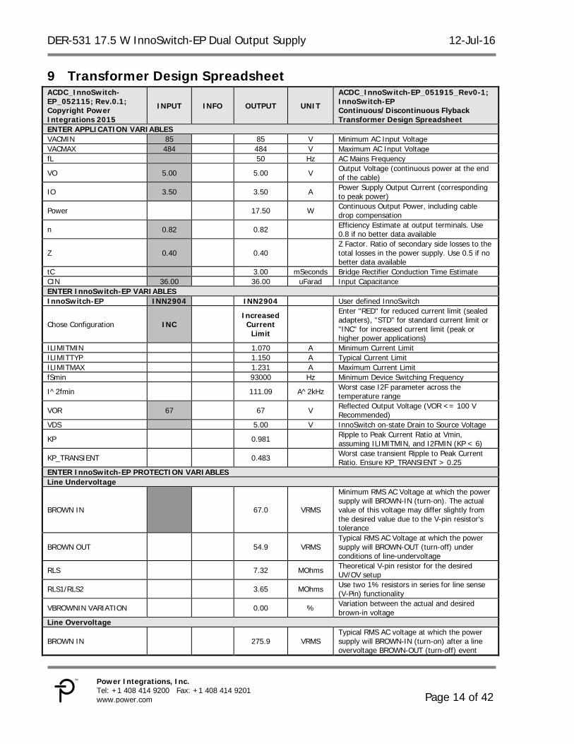
9 Transformer Design Spreadsheet ACDC_InnoSwitch-EP_052115; Rev.0.1; Copyright Power Integrations 2015
INPUT INFO OUTPUT UNIT
ACDC_InnoSwitch-EP_051915_Rev0-1; InnoSwitch-EP Continuous/Discontinuous Flyback Transformer Design Spreadsheet
ENTER APPLICATION VARIABLES VACMIN 85 85 V Minimum AC Input Voltage VACMAX 484 484 V Maximum AC Input Voltage fL 50 Hz AC Mains Frequency
VO 5.00 5.00 V Output Voltage (continuous power at the end of the cable)
IO 3.50 3.50 A Power Supply Output Current (corresponding to peak power)
Power 17.50 W Continuous Output Power, including cable drop compensation
n 0.82 0.82 Efficiency Estimate at output terminals. Use 0.8 if no better data available
Z 0.40 0.40 Z Factor. Ratio of secondary side losses to the total losses in the power supply. Use 0.5 if no better data available
tC 3.00 mSeconds Bridge Rectifier Conduction Time Estimate CIN 36.00 36.00 uFarad Input Capacitance ENTER InnoSwitch-EP VARIABLES InnoSwitch-EP INN2904 INN2904 User defined InnoSwitch
Chose Configuration INC Increased
Current Limit
Enter "RED" for reduced current limit (sealed adapters), "STD" for standard current limit or "INC" for increased current limit (peak or higher power applications)
ILIMITMIN 1.070 A Minimum Current Limit ILIMITTYP 1.150 A Typical Current Limit ILIMITMAX 1.231 A Maximum Current Limit fSmin 93000 Hz Minimum Device Switching Frequency
I^2fmin 111.09 A^2kHz Worst case I2F parameter across the temperature range
VOR 67 67 V Reflected Output Voltage (VOR <= 100 V Recommended)
VDS 5.00 V InnoSwitch on-state Drain to Source Voltage
KP 0.981 Ripple to Peak Current Ratio at Vmin, assuming ILIMITMIN, and I2FMIN (KP < 6)
KP_TRANSIENT 0.483 Worst case transient Ripple to Peak Current Ratio. Ensure KP_TRANSIENT > 0.25
ENTER InnoSwitch-EP PROTECTION VARIABLES Line Undervoltage
BROWN IN 67.0 VRMS
Minimum RMS AC Voltage at which the power supply will BROWN-IN (turn-on). The actual value of this voltage may differ slightly from the desired value due to the V-pin resistor's tolerance
BROWN OUT 54.9 VRMS Typical RMS AC Voltage at which the power supply will BROWN-OUT (turn-off) under conditions of line-undervoltage
RLS 7.32 MOhms Theoretical V-pin resistor for the desired UV/OV setup
RLS1/RLS2 3.65 MOhms Use two 1% resistors in series for line sense (V-Pin) functionality
VBROWNIN VARIATION 0.00 % Variation between the actual and desired brown-in voltage
Line Overvoltage
BROWN IN 275.9 VRMS Typical RMS AC voltage at which the power supply will BROWN-IN (turn-on) after a line overvoltage BROWN-OUT (turn-off) event
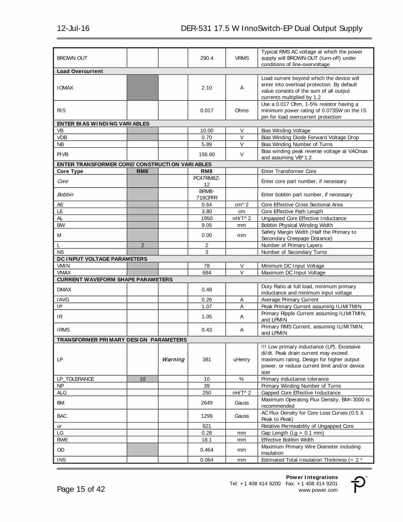
12-Jul-16 DER-531 17.5 W InnoSwitch-EP Dual Output Supply
Page 15 of 42
Power Integrations Tel: +1 408 414 9200 Fax: +1 408 414 9201
www.power.com
BROWN OUT 290.4 VRMS Typical RMS AC voltage at which the power supply will BROWN-OUT (turn-off) under conditions of line-overvoltage
Load Overcurrent
IOMAX 2.10 A
Load current beyond which the device will enter into overload protection. By default value consists of the sum of all output currents multiplied by 1.2
RIS 0.017 Ohms Use a 0.017 Ohm, 1-5% resistor having a minimum power rating of 0.0735W on the IS pin for load overcurrent protection
ENTER BIAS WINDING VARIABLES VB 10.00 V Bias Winding Voltage VDB 0.70 V Bias Winding Diode Forward Voltage Drop NB 5.89 V Bias Winding Number of Turns
PIVB 156.60 V Bias winding peak reverse voltage at VACmax and assuming VB*1.2
ENTER TRANSFORMER CORE/CONSTRUCTION VARIABLES Core Type RM8 RM8 Enter Transformer Core
Core PC47RM8Z-12 Enter core part number, if necessary
Bobbin BRM8-718CPFR Enter bobbin part number, if necessary
AE 0.64 cm^2 Core Effective Cross Sectional Area LE 3.80 cm Core Effective Path Length AL 1950 nH/T^2 Ungapped Core Effective Inductance BW 9.05 mm Bobbin Physical Winding Width
M 0.00 mm Safety Margin Width (Half the Primary to Secondary Creepage Distance)
L 2 2 Number of Primary Layers NS 3 Number of Secondary Turns DC INPUT VOLTAGE PARAMETERS VMIN 78 V Minimum DC Input Voltage VMAX 684 V Maximum DC Input Voltage CURRENT WAVEFORM SHAPE PARAMETERS
DMAX 0.48 Duty Ratio at full load, minimum primary inductance and minimum input voltage
IAVG 0.26 A Average Primary Current IP 1.07 A Peak Primary Current assuming ILIMITMIN
IR 1.05 A Primary Ripple Current assuming ILIMITMIN, and LPMIN
IRMS 0.43 A Primary RMS Current, assuming ILIMITMIN, and LPMIN
TRANSFORMER PRIMARY DESIGN PARAMETERS
LP Warning 381 uHenry
!!! Low primary inductance (LP), Excessive di/dt. Peak drain current may exceed maximum rating. Design for higher output power, or reduce current limit and/or device size
LP_TOLERANCE 10 10 % Primary inductance tolerance NP 39 Primary Winding Number of Turns ALG 250 nH/T^2 Gapped Core Effective Inductance
BM 2649 Gauss Maximum Operating Flux Density, BM<3000 is recommended
BAC 1299 Gauss AC Flux Density for Core Loss Curves (0.5 X Peak to Peak)
ur 921 Relative Permeability of Ungapped Core LG 0.28 mm Gap Length (Lg > 0.1 mm) BWE 18.1 mm Effective Bobbin Width
OD 0.464 mm Maximum Primary Wire Diameter including insulation
INS 0.064 mm Estimated Total Insulation Thickness (= 2 *
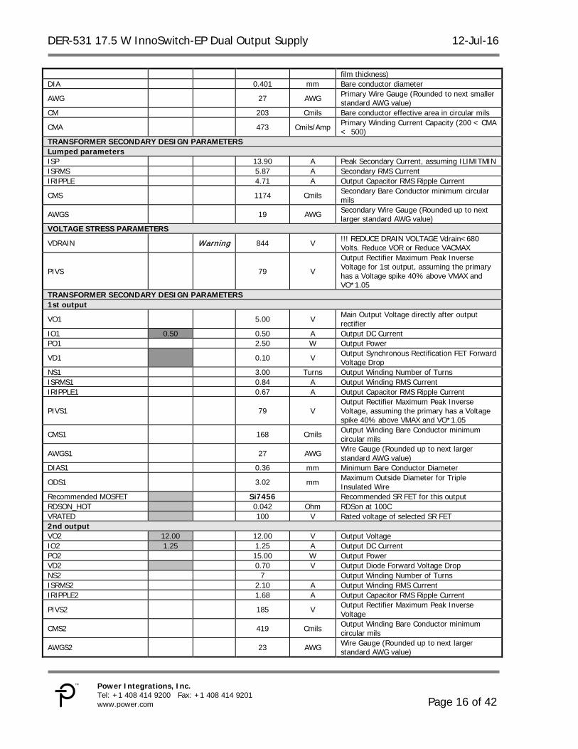
DER-531 17.5 W InnoSwitch-EP Dual Output Supply 12-Jul-16
Page 16 of 42
Power Integrations, Inc. Tel: +1 408 414 9200 Fax: +1 408 414 9201 www.power.com
film thickness) DIA 0.401 mm Bare conductor diameter
AWG 27 AWG Primary Wire Gauge (Rounded to next smaller standard AWG value)
CM 203 Cmils Bare conductor effective area in circular mils
CMA 473 Cmils/Amp Primary Winding Current Capacity (200 < CMA < 500)
TRANSFORMER SECONDARY DESIGN PARAMETERS Lumped parameters ISP 13.90 A Peak Secondary Current, assuming ILIMITMIN ISRMS 5.87 A Secondary RMS Current IRIPPLE 4.71 A Output Capacitor RMS Ripple Current
CMS 1174 Cmils Secondary Bare Conductor minimum circular mils
AWGS 19 AWG Secondary Wire Gauge (Rounded up to next larger standard AWG value)
VOLTAGE STRESS PARAMETERS
VDRAIN Warning 844 V !!! REDUCE DRAIN VOLTAGE Vdrain<680 Volts. Reduce VOR or Reduce VACMAX
PIVS 79 V
Output Rectifier Maximum Peak Inverse Voltage for 1st output, assuming the primary has a Voltage spike 40% above VMAX and VO*1.05
TRANSFORMER SECONDARY DESIGN PARAMETERS 1st output
VO1 5.00 V Main Output Voltage directly after output rectifier
IO1 0.50 0.50 A Output DC Current PO1 2.50 W Output Power
VD1 0.10 V Output Synchronous Rectification FET Forward Voltage Drop
NS1 3.00 Turns Output Winding Number of Turns ISRMS1 0.84 A Output Winding RMS Current IRIPPLE1 0.67 A Output Capacitor RMS Ripple Current
PIVS1 79 V Output Rectifier Maximum Peak Inverse Voltage, assuming the primary has a Voltage spike 40% above VMAX and VO*1.05
CMS1 168 Cmils Output Winding Bare Conductor minimum circular mils
AWGS1 27 AWG Wire Gauge (Rounded up to next larger standard AWG value)
DIAS1 0.36 mm Minimum Bare Conductor Diameter
ODS1 3.02 mm Maximum Outside Diameter for Triple Insulated Wire
Recommended MOSFET Si7456 Recommended SR FET for this output RDSON_HOT 0.042 Ohm RDSon at 100C VRATED 100 V Rated voltage of selected SR FET 2nd output VO2 12.00 12.00 V Output Voltage IO2 1.25 1.25 A Output DC Current PO2 15.00 W Output Power VD2 0.70 V Output Diode Forward Voltage Drop NS2 7 Output Winding Number of Turns ISRMS2 2.10 A Output Winding RMS Current IRIPPLE2 1.68 A Output Capacitor RMS Ripple Current
PIVS2 185 V Output Rectifier Maximum Peak Inverse Voltage
CMS2 419 Cmils Output Winding Bare Conductor minimum circular mils
AWGS2 23 AWG Wire Gauge (Rounded up to next larger standard AWG value)
12-Jul-16 DER-531 17.5 W InnoSwitch-EP Dual Output Supply
Page 17 of 42
Power Integrations Tel: +1 408 414 9200 Fax: +1 408 414 9201
www.power.com
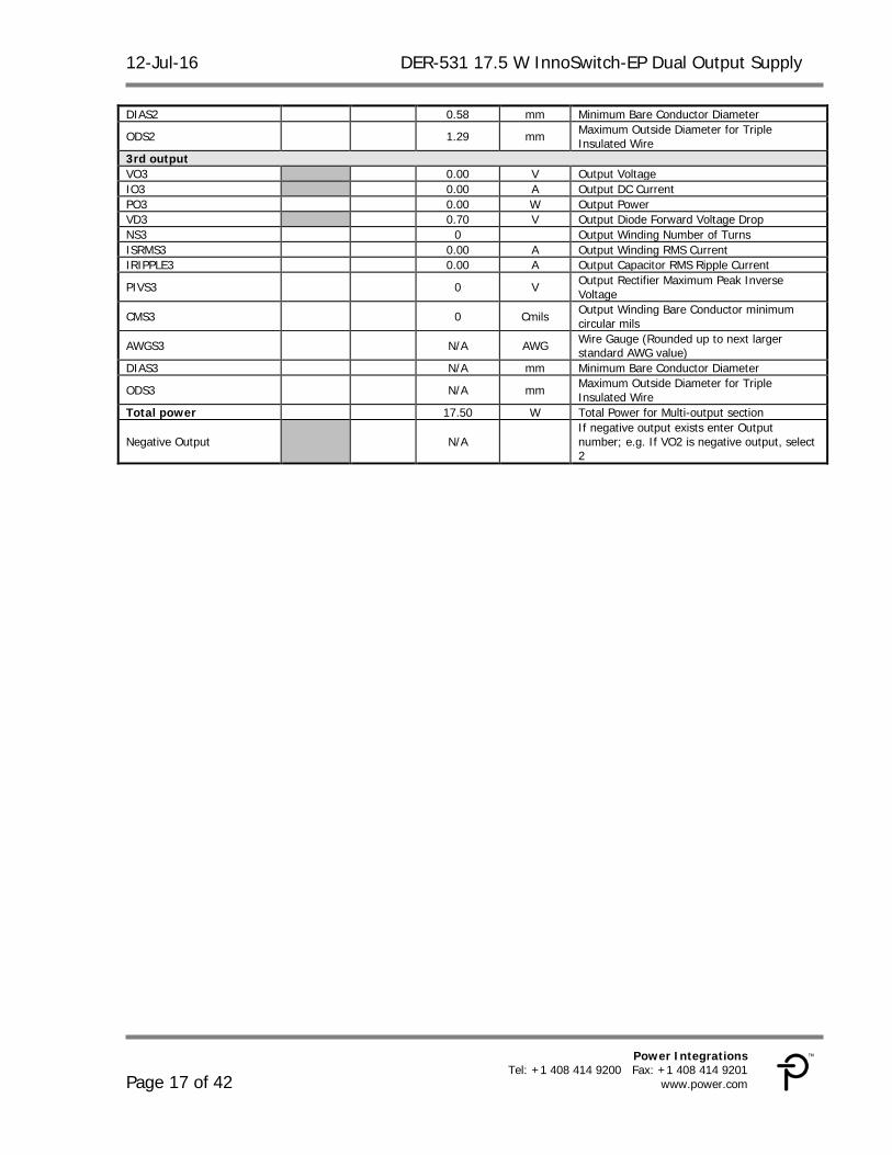
DIAS2 0.58 mm Minimum Bare Conductor Diameter
ODS2 1.29 mm Maximum Outside Diameter for Triple Insulated Wire
3rd output VO3 0.00 V Output Voltage IO3 0.00 A Output DC Current PO3 0.00 W Output Power VD3 0.70 V Output Diode Forward Voltage Drop NS3 0 Output Winding Number of Turns ISRMS3 0.00 A Output Winding RMS Current IRIPPLE3 0.00 A Output Capacitor RMS Ripple Current
PIVS3 0 V Output Rectifier Maximum Peak Inverse Voltage
CMS3 0 Cmils Output Winding Bare Conductor minimum circular mils
AWGS3 N/A AWG Wire Gauge (Rounded up to next larger standard AWG value)
DIAS3 N/A mm Minimum Bare Conductor Diameter
ODS3 N/A mm Maximum Outside Diameter for Triple Insulated Wire
Total power 17.50 W Total Power for Multi-output section
Negative Output N/A If negative output exists enter Output number; e.g. If VO2 is negative output, select 2
DER-531 17.5 W InnoSwitch-EP Dual Output Supply 12-Jul-16
Page 18 of 42
Power Integrations, Inc. Tel: +1 408 414 9200 Fax: +1 408 414 9201 www.power.com
10 Performance Data
Full Load Efficiency vs. Line 10.1
Figure 9 – Full load Efficiency vs. Line Voltage, Room Temperature.
76
78
80
82
84
86
88
90
92
70 110 150 190 230 270 310 350 390 430 470 510
Effi
cien
cy (
%)
Input Voltage (VAC)
Line Efficiency
12-Jul-16 DER-531 17.5 W InnoSwitch-EP Dual Output Supply
Page 19 of 42
Power Integrations Tel: +1 408 414 9200 Fax: +1 408 414 9201
www.power.com
No-Load Input Power 10.2
Figure 10 – No-Load Input Power vs. Input Line Voltage, Room Temperature.
0
50
100
150
200
250
300
350
400
70 90 110 130 150 170 190 210 230 250 270 290
Inpu
t P
ower
(m
W)
Input Voltage (VAC)
DER-531 17.5 W InnoSwitch-EP Dual Output Supply 12-Jul-16
Page 20 of 42
Power Integrations, Inc. Tel: +1 408 414 9200 Fax: +1 408 414 9201 www.power.com
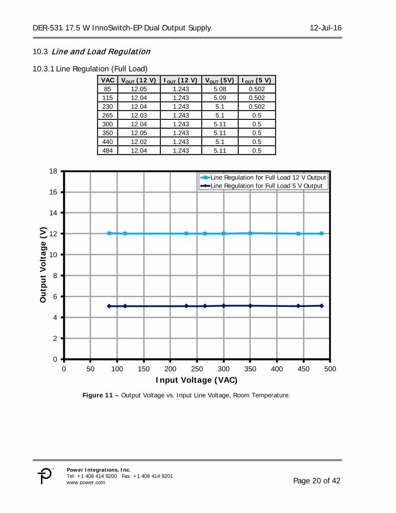
Line and Load Regulation 10.3
10.3.1 Line Regulation (Full Load) VAC VOUT (12 V) IOUT (12 V) VOUT (5V) IOUT (5 V) 85 12.05 1.243 5.08 0.502 115 12.04 1.243 5.09 0.502 230 12.04 1.243 5.1 0.502 265 12.03 1.243 5.1 0.5 300 12.04 1.243 5.11 0.5 350 12.05 1.243 5.11 0.5 440 12.02 1.243 5.1 0.5 484 12.04 1.243 5.11 0.5
Figure 11 – Output Voltage vs. Input Line Voltage, Room Temperature.
0
2
4
6
8
10
12
14
16
18
0 50 100 150 200 250 300 350 400 450 500
Out
put
Vol
tage
(V
)
Input Voltage (VAC)
Line Regulation for Full Load 12 V OutputLine Regulation for Full Load 5 V Output
12-Jul-16 DER-531 17.5 W InnoSwitch-EP Dual Output Supply
Page 21 of 42
Power Integrations Tel: +1 408 414 9200 Fax: +1 408 414 9201
www.power.com
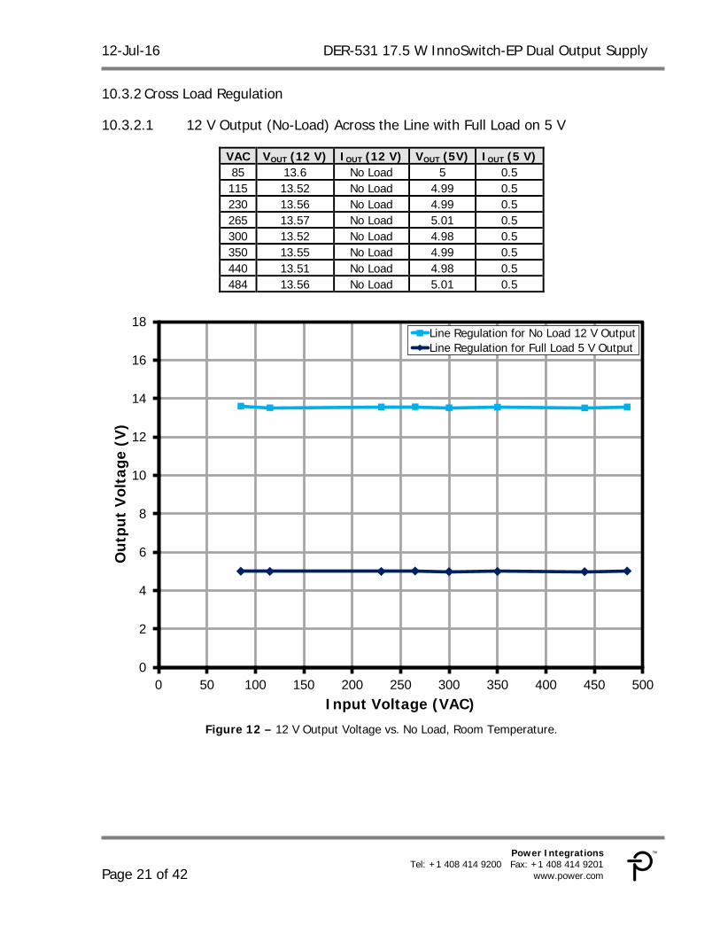
10.3.2 Cross Load Regulation
10.3.2.1 12 V Output (No-Load) Across the Line with Full Load on 5 V
VAC VOUT (12 V) IOUT (12 V) VOUT (5V) IOUT (5 V) 85 13.6 No Load 5 0.5 115 13.52 No Load 4.99 0.5 230 13.56 No Load 4.99 0.5 265 13.57 No Load 5.01 0.5 300 13.52 No Load 4.98 0.5 350 13.55 No Load 4.99 0.5 440 13.51 No Load 4.98 0.5 484 13.56 No Load 5.01 0.5
Figure 12 – 12 V Output Voltage vs. No Load, Room Temperature.
0
2
4
6
8
10
12
14
16
18
0 50 100 150 200 250 300 350 400 450 500
Out
put
Vol
tage
(V
)
Input Voltage (VAC)
Line Regulation for No Load 12 V OutputLine Regulation for Full Load 5 V Output
DER-531 17.5 W InnoSwitch-EP Dual Output Supply 12-Jul-16
Page 22 of 42
Power Integrations, Inc. Tel: +1 408 414 9200 Fax: +1 408 414 9201 www.power.com
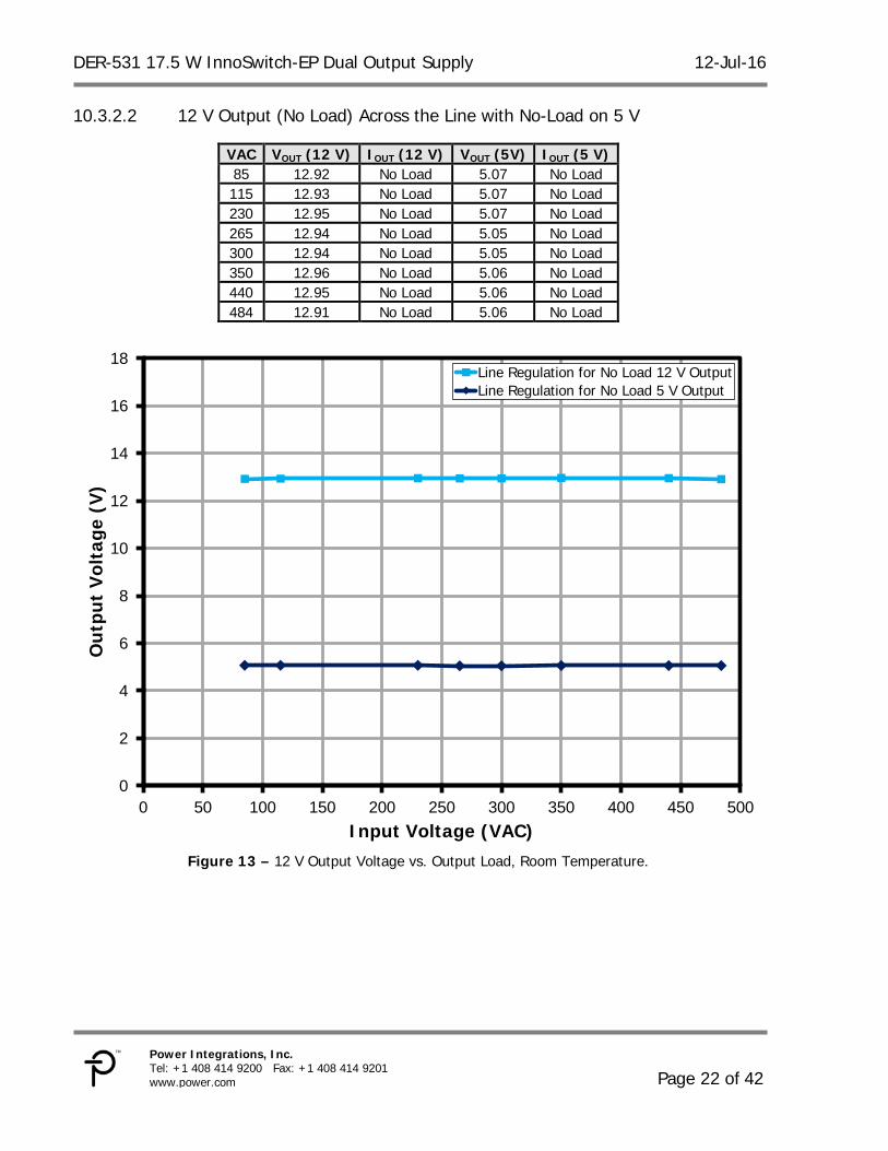
10.3.2.2 12 V Output (No Load) Across the Line with No-Load on 5 V
VAC VOUT (12 V) IOUT (12 V) VOUT (5V) IOUT (5 V) 85 12.92 No Load 5.07 No Load 115 12.93 No Load 5.07 No Load 230 12.95 No Load 5.07 No Load 265 12.94 No Load 5.05 No Load 300 12.94 No Load 5.05 No Load 350 12.96 No Load 5.06 No Load 440 12.95 No Load 5.06 No Load 484 12.91 No Load 5.06 No Load
Figure 13 – 12 V Output Voltage vs. Output Load, Room Temperature.
0
2
4
6
8
10
12
14
16
18
0 50 100 150 200 250 300 350 400 450 500
Out
put
Vol
tage
(V
)
Input Voltage (VAC)
Line Regulation for No Load 12 V OutputLine Regulation for No Load 5 V Output
12-Jul-16 DER-531 17.5 W InnoSwitch-EP Dual Output Supply
Page 23 of 42
Power Integrations Tel: +1 408 414 9200 Fax: +1 408 414 9201
www.power.com
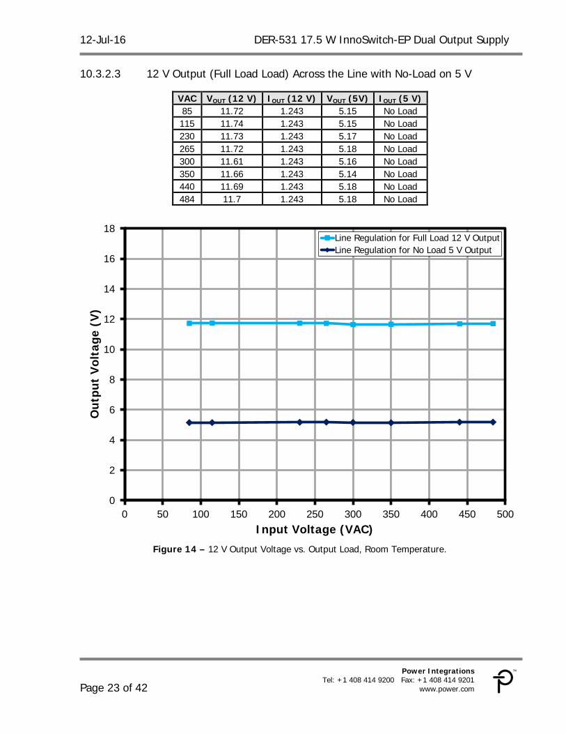
10.3.2.3 12 V Output (Full Load Load) Across the Line with No-Load on 5 V
VAC VOUT (12 V) IOUT (12 V) VOUT (5V) IOUT (5 V) 85 11.72 1.243 5.15 No Load 115 11.74 1.243 5.15 No Load 230 11.73 1.243 5.17 No Load 265 11.72 1.243 5.18 No Load 300 11.61 1.243 5.16 No Load 350 11.66 1.243 5.14 No Load 440 11.69 1.243 5.18 No Load 484 11.7 1.243 5.18 No Load
Figure 14 – 12 V Output Voltage vs. Output Load, Room Temperature.
0
2
4
6
8
10
12
14
16
18
0 50 100 150 200 250 300 350 400 450 500
Out
put
Vol
tage
(V
)
Input Voltage (VAC)
Line Regulation for Full Load 12 V OutputLine Regulation for No Load 5 V Output
DER-531 17.5 W InnoSwitch-EP Dual Output Supply 12-Jul-16
Page 24 of 42
Power Integrations, Inc. Tel: +1 408 414 9200 Fax: +1 408 414 9201 www.power.com
11 Thermal Performance
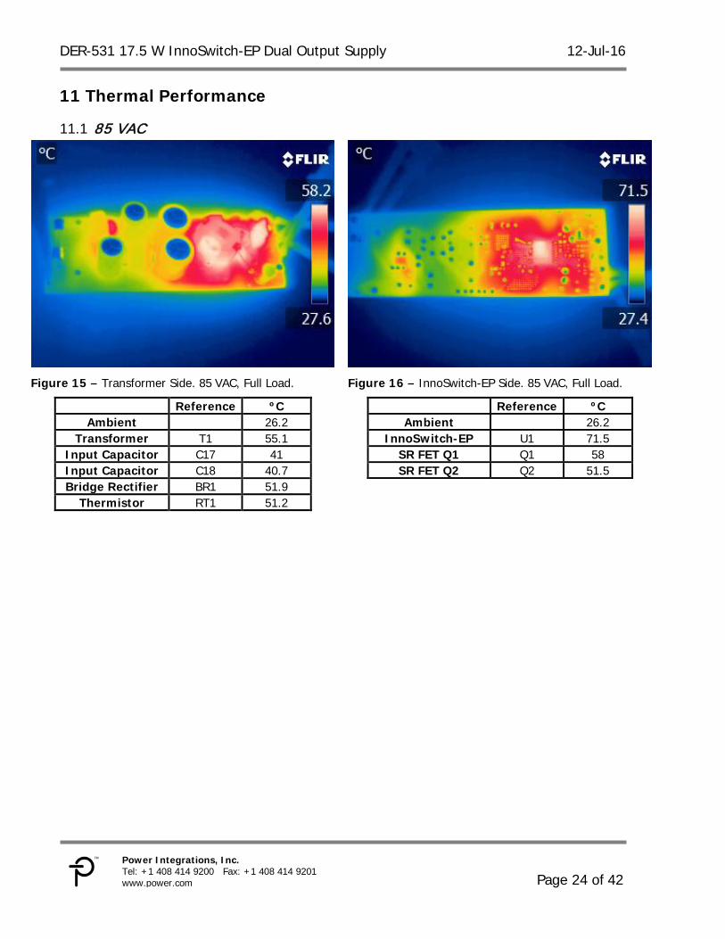
85 VAC 11.1
Figure 15 – Transformer Side. 85 VAC, Full Load.
Reference ºC Ambient 26.2
Transformer T1 55.1 Input Capacitor C17 41 Input Capacitor C18 40.7 Bridge Rectifier BR1 51.9
Thermistor RT1 51.2
Figure 16 – InnoSwitch-EP Side. 85 VAC, Full Load.
Reference ºC Ambient 26.2
InnoSwitch-EP U1 71.5 SR FET Q1 Q1 58 SR FET Q2 Q2 51.5
12-Jul-16 DER-531 17.5 W InnoSwitch-EP Dual Output Supply
Page 25 of 42
Power Integrations Tel: +1 408 414 9200 Fax: +1 408 414 9201
www.power.com
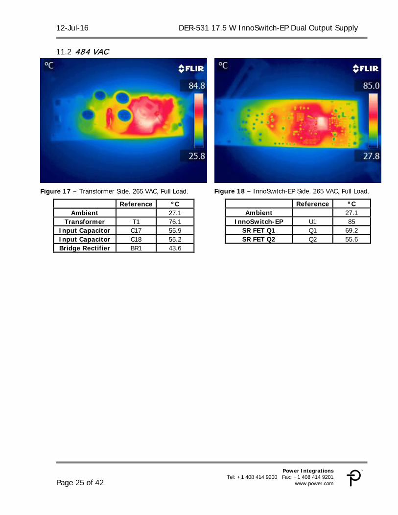
484 VAC 11.2
Figure 17 – Transformer Side. 265 VAC, Full Load.
Reference ºC Ambient 27.1
Transformer T1 76.1 Input Capacitor C17 55.9 Input Capacitor C18 55.2 Bridge Rectifier BR1 43.6
Figure 18 – InnoSwitch-EP Side. 265 VAC, Full Load.
Reference ºC Ambient 27.1
InnoSwitch-EP U1 85 SR FET Q1 Q1 69.2 SR FET Q2 Q2 55.6
DER-531 17.5 W InnoSwitch-EP Dual Output Supply 12-Jul-16
Page 26 of 42
Power Integrations, Inc. Tel: +1 408 414 9200 Fax: +1 408 414 9201 www.power.com
12 Output Power vs. Thermal Rise at 85º Ambient for Different AC Input Voltages Input Voltage(VAC) Output Power(W) T(amb) in (ºC) T(Inno) in (ºC) dT(Rise)
484 5.8 85.5 109.8 24.3 440 6.94 85.2 110.1 24.9 350 9.54 85.1 109.2 24.1 265 11.4 85.2 109 23.8 85 10.12 85.5 109.5 24
Note: All the measurements are done using thermo couples.
12-Jul-16 DER-531 17.5 W InnoSwitch-EP Dual Output Supply
Page 27 of 42
Power Integrations Tel: +1 408 414 9200 Fax: +1 408 414 9201
www.power.com
13 Waveforms
Load Transient Response 13.1
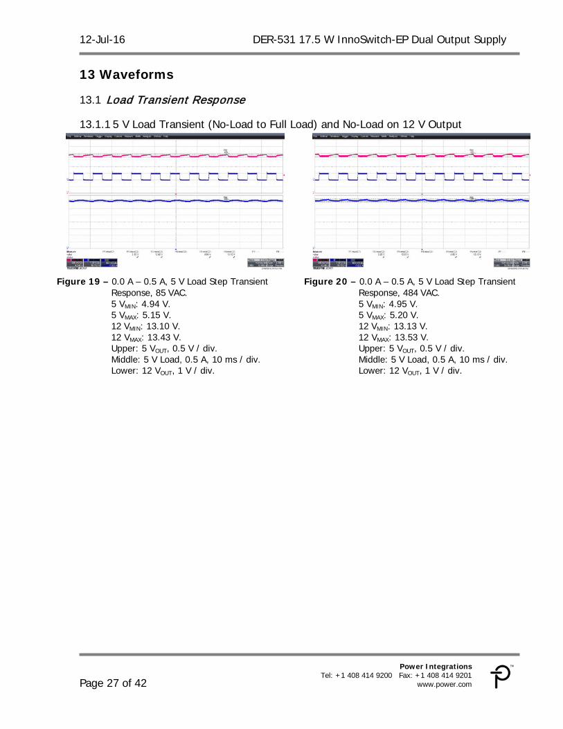
13.1.1 5 V Load Transient (No-Load to Full Load) and No-Load on 12 V Output
Figure 19 – 0.0 A – 0.5 A, 5 V Load Step Transient
Response, 85 VAC. 5 VMIN: 4.94 V. 5 VMAX: 5.15 V. 12 VMIN: 13.10 V. 12 VMAX: 13.43 V. Upper: 5 VOUT, 0.5 V / div. Middle: 5 V Load, 0.5 A, 10 ms / div. Lower: 12 VOUT, 1 V / div.
Figure 20 – 0.0 A – 0.5 A, 5 V Load Step Transient Response, 484 VAC. 5 VMIN: 4.95 V. 5 VMAX: 5.20 V. 12 VMIN: 13.13 V. 12 VMAX: 13.53 V. Upper: 5 VOUT, 0.5 V / div. Middle: 5 V Load, 0.5 A, 10 ms / div. Lower: 12 VOUT, 1 V / div.
DER-531 17.5 W InnoSwitch-EP Dual Output Supply 12-Jul-16
Page 28 of 42
Power Integrations, Inc. Tel: +1 408 414 9200 Fax: +1 408 414 9201 www.power.com
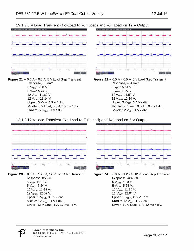
13.1.2 5 V Load Transient (No-Load to Full Load) and Full Load on 12 V Output
Figure 21 – 0.0 A – 0.5 A, 5 V Load Step Transient
Response, 85 VAC. 5 VMIN: 5.00 V. 5 VMAX: 5.24 V. 12 VMIN: 11.60 V. 12 VMAX: 12.14 V. Upper: 5 VOUT, 0.5 V / div. Middle: 5 V Load, 0.5 A, 10 ms / div. Lower: 12 VOUT, 1 V / div.
Figure 22 – 0.0 A – 0.5 A, 5 V Load Step Transient Response, 484 VAC. 5 VMIN: 5.04 V. 5 VMAX: 5.27 V. 12 VMIN: 11.57 V. 12 VMAX: 12.10 V. Upper: 5 VOUT, 0.5 V / div. Middle: 5 V Load, 0.5 A, 10 ms / div. Lower: 12 VOUT, 1 V / div.
13.1.3 12 V Load Transient (No-Load to Full Load) and No-Load on 5 V Output
Figure 23 – 0.0 A – 1.25 A, 12 V Load Step Transient
Response, 85 VAC. 5 VMIN: 5.10 V. 5 VMAX: 5.24 V. 12 VMIN: 11.64 V. 12 VMAX: 12.07 V. Upper: 5 VOUT, 0.5 V / div. Middle: 12 VOUT, 1 V / div. Lower: 12 V Load, 1 A, 10 ms / div.
Figure 24 – 0.0 A – 1.25 A, 12 V Load Step Transient Response, 484 VAC. 5 VMIN: 5.10 V. 5 VMAX: 5.24 V. 12 VMIN: 11.60 V. 12 VMAX: 12.04 V. Upper: 5 VOUT, 0.5 V / div. Middle: 12 VOUT, 1 V / div. Lower: 12 V Load, 1 A, 10 ms / div.
12-Jul-16 DER-531 17.5 W InnoSwitch-EP Dual Output Supply
Page 29 of 42
Power Integrations Tel: +1 408 414 9200 Fax: +1 408 414 9201
www.power.com
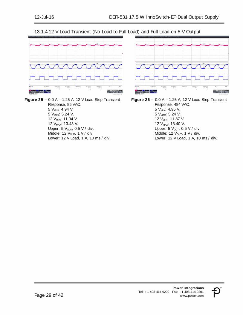
13.1.4 12 V Load Transient (No-Load to Full Load) and Full Load on 5 V Output
Figure 25 – 0.0 A – 1.25 A, 12 V Load Step Transient
Response, 85 VAC. 5 VMIN: 4.94 V. 5 VMAX: 5.24 V. 12 VMIN: 11.94 V. 12 VMAX: 13.43 V. Upper: 5 VOUT, 0.5 V / div. Middle: 12 VOUT, 1 V / div. Lower: 12 V Load, 1 A, 10 ms / div.
Figure 26 – 0.0 A – 1.25 A, 12 V Load Step Transient Response, 484 VAC. 5 VMIN: 4.95 V. 5 VMAX: 5.24 V. 12 VMIN: 11.87 V. 12 VMAX: 13.40 V. Upper: 5 VOUT, 0.5 V / div. Middle: 12 VOUT, 1 V / div. Lower: 12 V Load, 1 A, 10 ms / div.
DER-531 17.5 W InnoSwitch-EP Dual Output Supply 12-Jul-16
Page 30 of 42
Power Integrations, Inc. Tel: +1 408 414 9200 Fax: +1 408 414 9201 www.power.com
Sw itching Waveforms 13.2
13.2.1 InnoSwitch-EP Waveforms
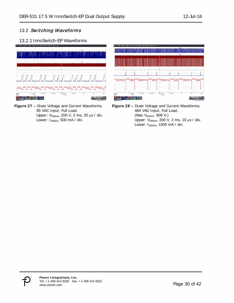
Figure 27 – Drain Voltage and Current Waveforms.
85 VAC Input, Full Load. Upper: VDRAIN, 200 V, 2 ms, 20 µs / div. Lower: IDRAIN, 500 mA / div.
Figure 28 – Drain Voltage and Current Waveforms. 484 VAC Input, Full Load, (Max VDRAIN: 806 V.) Upper: VDRAIN, 200 V, 2 ms, 10 µs / div. Lower: IDRAIN, 1000 mA / div.
12-Jul-16 DER-531 17.5 W InnoSwitch-EP Dual Output Supply
Page 31 of 42
Power Integrations Tel: +1 408 414 9200 Fax: +1 408 414 9201
www.power.com
13.2.2 SR FET Waveforms
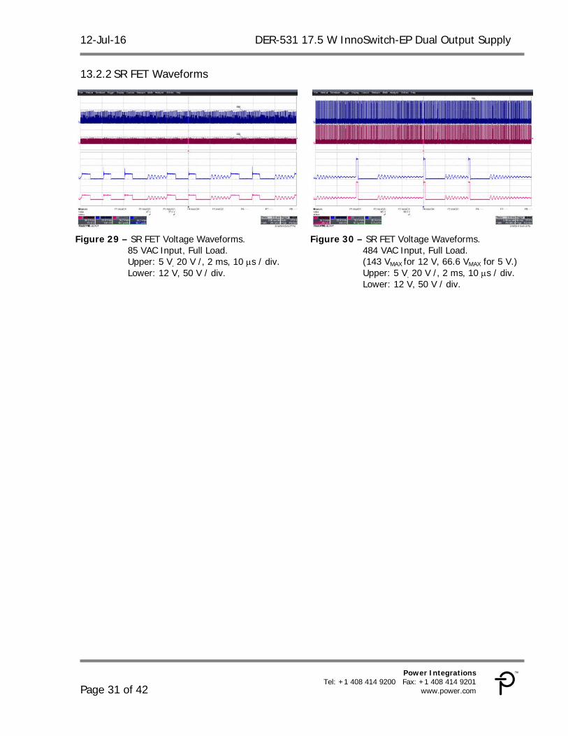
Figure 29 – SR FET Voltage Waveforms.
85 VAC Input, Full Load. Upper: 5 V, 20 V /, 2 ms, 10 µs / div. Lower: 12 V, 50 V / div.
Figure 30 – SR FET Voltage Waveforms. 484 VAC Input, Full Load. (143 VMAX for 12 V, 66.6 VMAX for 5 V.) Upper: 5 V, 20 V /, 2 ms, 10 µs / div. Lower: 12 V, 50 V / div.
DER-531 17.5 W InnoSwitch-EP Dual Output Supply 12-Jul-16
Page 32 of 42
Power Integrations, Inc. Tel: +1 408 414 9200 Fax: +1 408 414 9201 www.power.com
13.2.3 Output Voltage and Current Waveforms During Start-Up
13.2.3.1 Full load
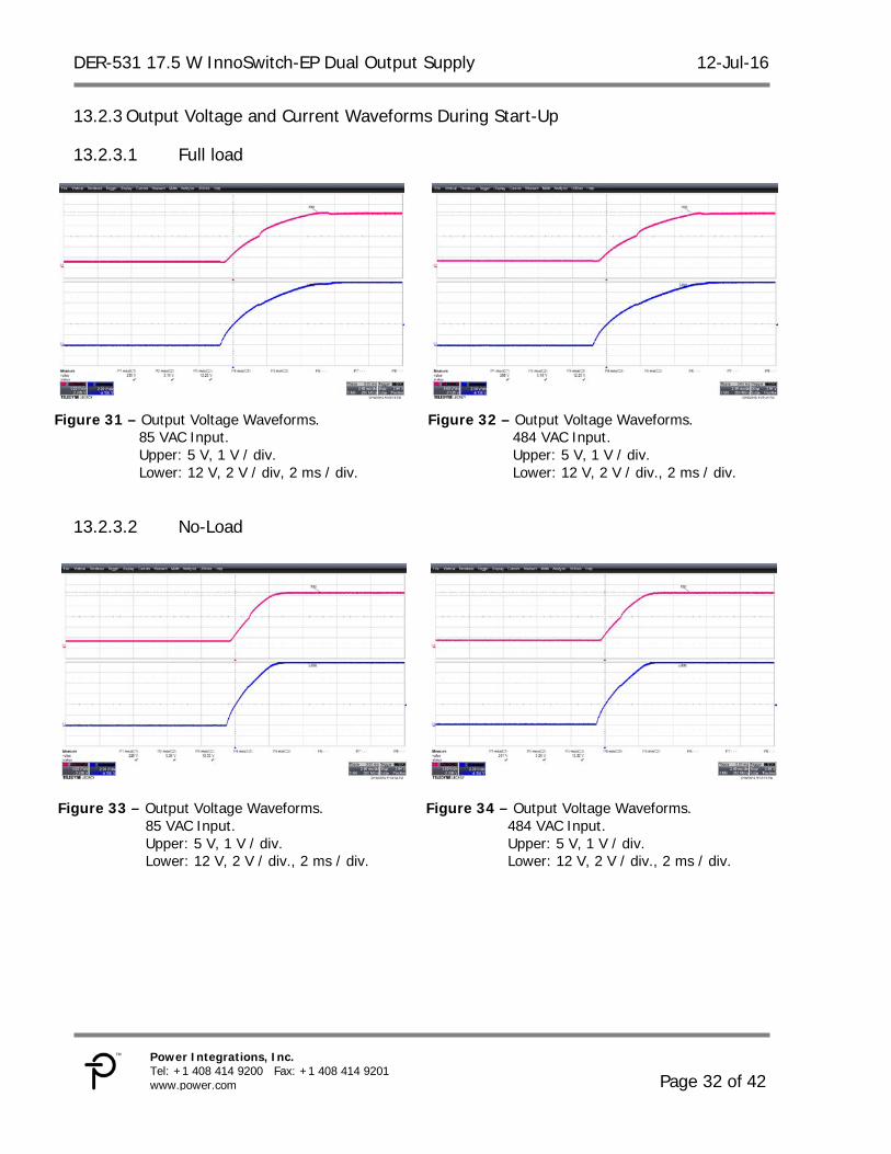
Figure 31 – Output Voltage Waveforms.
85 VAC Input. Upper: 5 V, 1 V / div. Lower: 12 V, 2 V / div, 2 ms / div.
Figure 32 – Output Voltage Waveforms. 484 VAC Input. Upper: 5 V, 1 V / div. Lower: 12 V, 2 V / div., 2 ms / div.
13.2.3.2 No-Load
Figure 33 – Output Voltage Waveforms. 85 VAC Input. Upper: 5 V, 1 V / div. Lower: 12 V, 2 V / div., 2 ms / div.
Figure 34 – Output Voltage Waveforms. 484 VAC Input. Upper: 5 V, 1 V / div. Lower: 12 V, 2 V / div., 2 ms / div.
12-Jul-16 DER-531 17.5 W InnoSwitch-EP Dual Output Supply
Page 33 of 42
Power Integrations Tel: +1 408 414 9200 Fax: +1 408 414 9201
www.power.com
Output Ripple Measurements 13.3
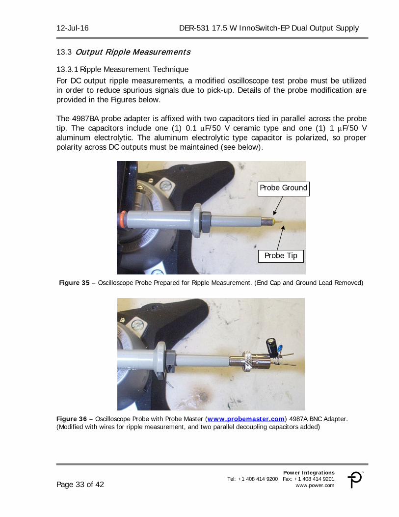
13.3.1 Ripple Measurement Technique For DC output ripple measurements, a modified oscilloscope test probe must be utilized in order to reduce spurious signals due to pick-up. Details of the probe modification are provided in the Figures below. The 4987BA probe adapter is affixed with two capacitors tied in parallel across the probe tip. The capacitors include one (1) 0.1 µF/50 V ceramic type and one (1) 1 µF/50 V aluminum electrolytic. The aluminum electrolytic type capacitor is polarized, so proper polarity across DC outputs must be maintained (see below).
Figure 35 – Oscilloscope Probe Prepared for Ripple Measurement. (End Cap and Ground Lead Removed)
Figure 36 – Oscilloscope Probe with Probe Master (www.probemaster.com) 4987A BNC Adapter. (Modified with wires for ripple measurement, and two parallel decoupling capacitors added)
Probe Ground
Probe Tip
DER-531 17.5 W InnoSwitch-EP Dual Output Supply 12-Jul-16
Page 34 of 42
Power Integrations, Inc. Tel: +1 408 414 9200 Fax: +1 408 414 9201 www.power.com
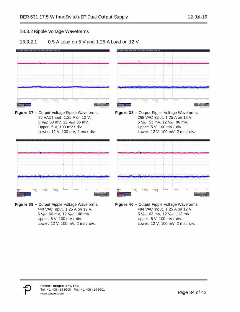
13.3.2 Ripple Voltage Waveforms
13.3.2.1 0.5 A Load on 5 V and 1.25 A Load on 12 V
Figure 37 – Output Voltage Ripple Waveforms.
85 VAC Input. 1.25 A on 12 V. 5 VPK: 50 mV, 12 VPK: 86 mV. Upper: 5 V, 100 mV / div. Lower: 12 V, 100 mV, 2 ms / div.
Figure 38 – Output Ripple Voltage Waveforms. 265 VAC Input. 1.25 A on 12 V. 5 VPK: 53 mV, 12 VPK: 96 mV. Upper: 5 V, 100 mV / div. Lower: 12 V, 100 mV, 2 ms / div.
Figure 39 – Output Ripple Voltage Waveforms. 440 VAC Input. 1.25 A on 12 V. 5 VPK: 60 mV, 12 VPK: 106 mV. Upper: 5 V, 100 mV / div. Lower: 12 V, 100 mV, 2 ms / div.
Figure 40 – Output Ripple Voltage Waveforms. 484 VAC Input. 1.25 A on 12 V. 5 VPK: 63 mV, 12 VPK: 113 mV. Upper: 5 V, 100 mV / div. Lower: 12 V, 100 mV, 2 ms / div..
12-Jul-16 DER-531 17.5 W InnoSwitch-EP Dual Output Supply
Page 35 of 42
Power Integrations Tel: +1 408 414 9200 Fax: +1 408 414 9201
www.power.com
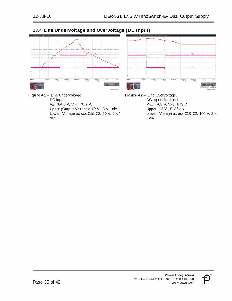
Line Undervoltage and Overvoltage (DC Input) 13.4
Figure 41 – Line Undervoltage.
DC Input. VUV+:84.0 V, VUV-: 70.2 V. Upper (Output Voltage): 12 V , 5 V / div. Lower: Voltage across C1& C2, 20 V, 2 s / div.
Figure 42 – Line Overvoltage. DC Input, No-Load. VOV+: 708 V, VOV-: 673 V. Upper: 12 V , 5 V / div. Lower: Voltage across C1& C2, 100 V, 2 s / div.
DER-531 17.5 W InnoSwitch-EP Dual Output Supply 12-Jul-16
Page 36 of 42
Power Integrations, Inc. Tel: +1 408 414 9200 Fax: +1 408 414 9201 www.power.com
14 ESD Passed ±16.5 kV air discharge and 8 kV contact discharge.
Air discharge (kV) Number of Strikes Test Result
+16.5 KV 10 PASS -16.5 KV 10 PASS
Contact discharge (kV) Number of Strikes Test Result
+8 KV 10 PASS -8 KV 10 PASS
15 EMI
Conductive EMI 15.1
15.1.1 Earth Grounded Output (QP / AV)
15.1.1.1 110 VAC Input, Neutral
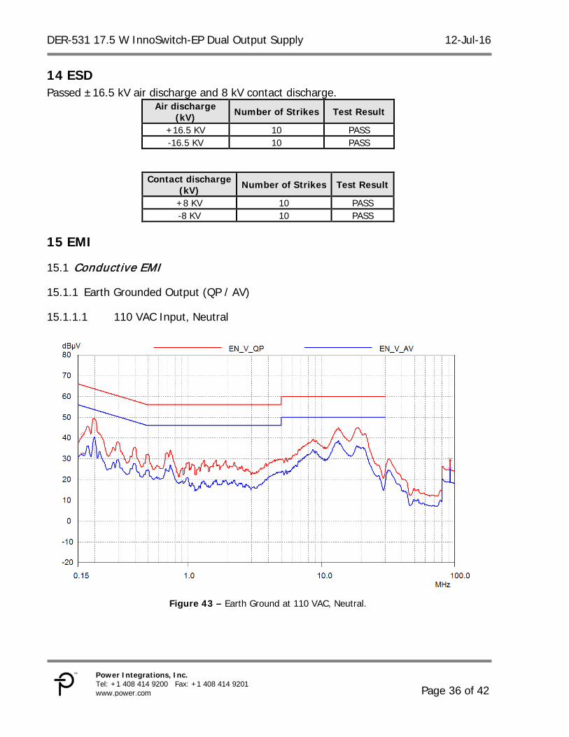
Figure 43 – Earth Ground at 110 VAC, Neutral.
12-Jul-16 DER-531 17.5 W InnoSwitch-EP Dual Output Supply
Page 37 of 42
Power Integrations Tel: +1 408 414 9200 Fax: +1 408 414 9201
www.power.com
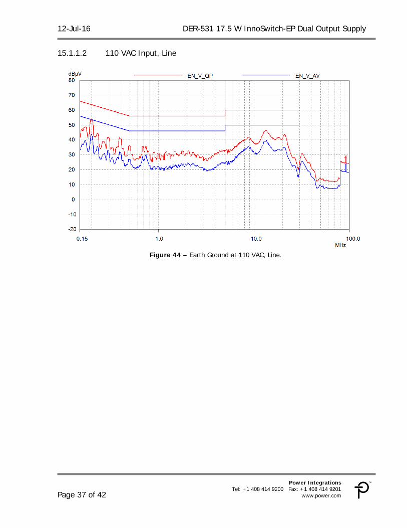
15.1.1.2 110 VAC Input, Line
Figure 44 – Earth Ground at 110 VAC, Line.
DER-531 17.5 W InnoSwitch-EP Dual Output Supply 12-Jul-16
Page 38 of 42
Power Integrations, Inc. Tel: +1 408 414 9200 Fax: +1 408 414 9201 www.power.com
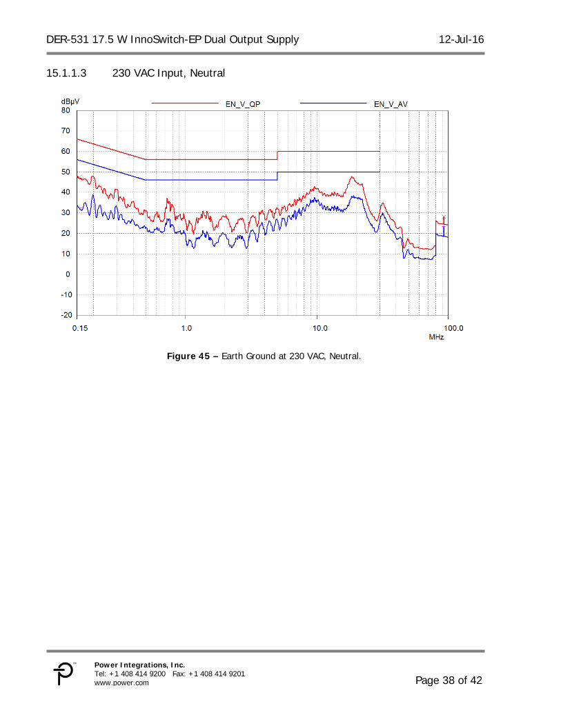
15.1.1.3 230 VAC Input, Neutral
Figure 45 – Earth Ground at 230 VAC, Neutral.
12-Jul-16 DER-531 17.5 W InnoSwitch-EP Dual Output Supply
Page 39 of 42
Power Integrations Tel: +1 408 414 9200 Fax: +1 408 414 9201
www.power.com
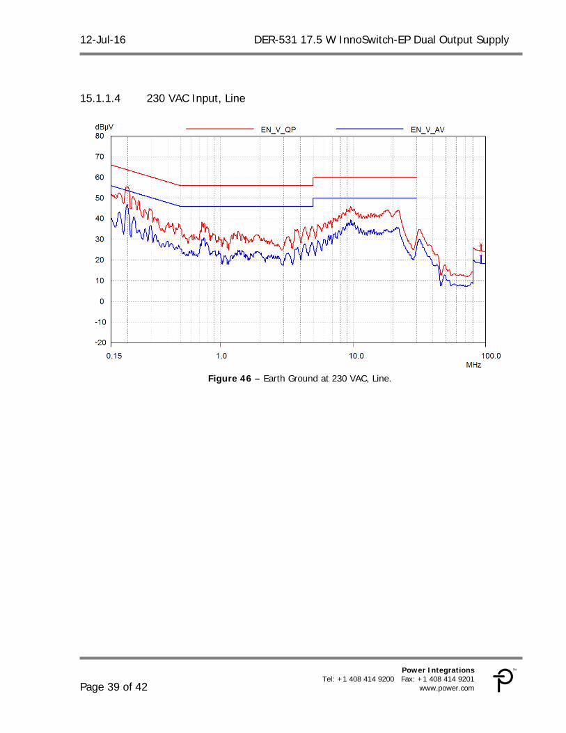
15.1.1.4 230 VAC Input, Line
Figure 46 – Earth Ground at 230 VAC, Line.
DER-531 17.5 W InnoSwitch-EP Dual Output Supply 12-Jul-16
Page 40 of 42
Power Integrations, Inc. Tel: +1 408 414 9200 Fax: +1 408 414 9201 www.power.com
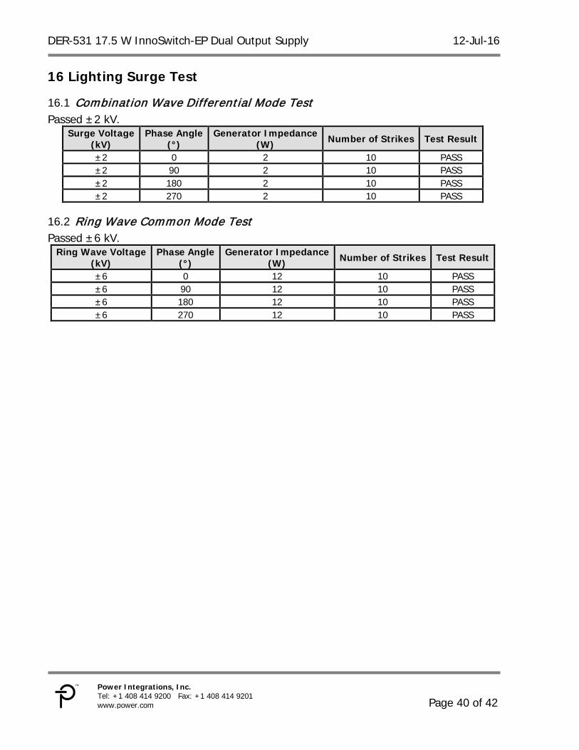
16 Lighting Surge Test
Combination Wave Differential Mode Test 16.1Passed ±2 kV.
Surge Voltage (kV)
Phase Angle (°)
Generator Impedance (W) Number of Strikes Test Result
±2 0 2 10 PASS ±2 90 2 10 PASS ±2 180 2 10 PASS ±2 270 2 10 PASS
Ring Wave Common Mode Test 16.2Passed ±6 kV.
Ring Wave Voltage (kV)
Phase Angle (°)
Generator Impedance (W) Number of Strikes Test Result
±6 0 12 10 PASS ±6 90 12 10 PASS ±6 180 12 10 PASS ±6 270 12 10 PASS
12-Jul-16 DER-531 17.5 W InnoSwitch-EP Dual Output Supply
Page 41 of 42
Power Integrations Tel: +1 408 414 9200 Fax: +1 408 414 9201
www.power.com
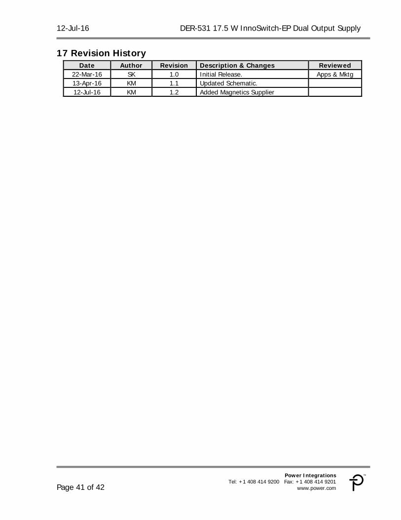
17 Revision History Date Author Revision Description & Changes Reviewed
22-Mar-16 SK 1.0 Initial Release. Apps & Mktg 13-Apr-16 KM 1.1 Updated Schematic. 12-Jul-16 KM 1.2 Added Magnetics Supplier
DER-531 17.5 W InnoSwitch-EP Dual Output Supply 12-Jul-16
Page 42 of 42
Power Integrations, Inc. Tel: +1 408 414 9200 Fax: +1 408 414 9201 www.power.com
For the latest updates, visit our website: www.power.com
Power Integrations reserves the right to make changes to its products at any time to improve reliability or manufacturability. Power Integrations does not assume any liability arising from the use of any device or circuit described herein. POWER INTEGRATIONS MAKES NO WARRANTY HEREIN AND SPECIFICALLY DISCLAIMS ALL WARRANTIES INCLUDING, WITHOUT LIMITATION, THE IMPLIED WARRANTIES OF MERCHANTABILITY, FITNESS FOR A PARTICULAR PURPOSE, AND NON-INFRINGEMENT OF THIRD PARTY RIGHTS.
Patent Information The products and applications illustrated herein (including transformer construction and circuits’ external to the products) may be covered by one or more U.S. and foreign patents, or potentially by pending U.S. and foreign patent applications assigned to Power Integrations. A complete list of Power Integrations’ patents may be found at www.power.com. Power Integrations grants its customers a license under certain patent rights as set forth at http://www.power.com/ip.htm.
The PI Logo, TOPSwitch, TinySwitch, LinkSwitch, LYTSwitch, InnoSwtich, DPA-Switch, PeakSwitch, CAPZero, SENZero, LinkZero, HiperPFS, HiperTFS, HiperLCS, Qspeed, EcoSmart, Clampless, E-Shield, Filterfuse, FluxLink, StackFET, PI Expert and PI FACTS are trademarks of Power Integrations, Inc. Other trademarks are property of their respective companies. ©Copyright 2015 Power Integrations, Inc.
Power Integrations Worldwide Sales Support Locations
WORLD HEADQUARTERS 5245 Hellyer Avenue San Jose, CA 95138, USA. Main: +1-408-414-9200 Customer Service: Phone: +1-408-414-9665 Fax: +1-408-414-9765 e-mail: [email protected]
GERMANY Lindwurmstrasse 114 80337, Munich Germany Phone: +49-895-527-39110 Fax: +49-895-527-39200 e-mail: [email protected]
JAPAN Kosei Dai-3 Building 2-12-11, Shin-Yokohama, Kohoku-ku, Yokohama-shi, Kanagawa 222-0033 Japan Phone: +81-45-471-1021 Fax: +81-45-471-3717 e-mail: [email protected]
TAIWAN 5F, No. 318, Nei Hu Rd., Sec. 1 Nei Hu District Taipei 11493, Taiwan R.O.C. Phone: +886-2-2659-4570 Fax: +886-2-2659-4550 e-mail: [email protected]
CHINA (SHANGHAI) Rm 2410, Charity Plaza, No. 88, North Caoxi Road, Shanghai, PRC 200030 Phone: +86-21-6354-6323 Fax: +86-21-6354-6325 e-mail: [email protected]
INDIA #1, 14th Main Road Vasanthanagar Bangalore-560052 India Phone: +91-80-4113-8020 Fax: +91-80-4113-8023 e-mail: [email protected]
KOREA RM 602, 6FL Korea City Air Terminal B/D, 159-6 Samsung-Dong, Kangnam-Gu, Seoul, 135-728 Korea Phone: +82-2-2016-6610 Fax: +82-2-2016-6630 e-mail: [email protected]
UK Cambridge Semiconductor, a Power Integrations company Westbrook Centre, Block 5, 2nd Floor Milton Road Cambridge CB4 1YG Phone: +44 (0) 1223-446483 e-mail: [email protected]
CHINA (SHENZHEN) 17/F, Hivac Building, No. 2, Keji Nan 8th Road, Nanshan District, Shenzhen, China, 518057 Phone: +86-755-8672-8689 Fax: +86-755-8672-8690 e-mail: [email protected]
ITALY Via Milanese 20, 3rd. Fl. 20099 Sesto San Giovanni (MI) Italy Phone: +39-024-550-8701 Fax: +39-028-928-6009 e-mail: [email protected]
SINGAPORE 51 Newton Road, #19-01/05 Goldhill Plaza Singapore, 308900 Phone: +65-6358-2160 Fax: +65-6358-2015 e-mail: [email protected]