Embed Size (px)
Citation preview

Deposition and Analysis of Zinc Oxide ThinFilms by Pulsed Laser Deposition
Diplomarbeit
Friedrich-Schiller-Universitat Jena
Physikalisch-Astronomische Fakultat
Institut fur Festkorperphysik
eingereicht von: Robert Pietzckergeboren am: 26.05.1981 in: Bonn

1. Gutachter: Prof. Dr. Paul Seidel2. Gutachter: PD Dr. Frank SchmidlTag der Verleihung des Diploms:

Erklarung
Ich erklare, dass ich die vorliegende Arbeit selbstandig verfasst und keine anderen alsdie angegebenen Quellen und Hilfsmittel benutzt habe.
Jena, den Unterschrift
Seitens des Verfassers bestehen keine Einwande, die vorliegende Diplomarbeit fur dieoffentliche Nutzung in der Thuringer Universitats- und Landesbibliothek zur Verfugungzu stellen.
Jena, den Unterschrift
III

Acknowledgments
I would like to express my gratitude to all those who assisted me academically andpersonally in finishing this part of my studies and completing this thesis.
My special thanks go to Prof. Dr. P. Seidel for the possibility to write my thesis inhis low temperature research group and for accepting the responsibility to supervise mywork.
I am deeply indebted to my direct supervisor, PD F. Schmidl, who inspired me toconduct research on thin films. He was always open for discussion, conveyed motivationand energy, and left me all the liberties for self-determined work.
My thanks go to Mr. Hanse, who designed and fabricated all parts needed for thechanges to the PLD setup, and Lutz Follmer and Torsten Hilbrecht, who tirelesslyhelped when problems with the PLD setup occurred.
To Dr. Kraußlich for his advice on XRD measurements.To Ms. Voigt for the Dektak and AFM measurements.To Veit Grosse, for his guidance and advice in all things PLD- and YBCO-related.To Micha Mans, for his unlimited willingness to help and and his patience to endure
my questions and music.To Gabriel Zieger, who assisted me in unraveling the mysteries of PLD and scientific
work, and who was there whenever I needed help to rebuild the setup or discuss physics,environmental science or politics.
To the whole research group for the great atmosphere and the absolute willingness tohelp each other.
To my parents, whose support (both moral and monetary) enabled me to study physicsand write this thesis.
To Michala Garbe, without whom this thesis would never have been created.To my roommates, who were a source of joy and laughter and always there when I
needed a diversion from physics.To Vroni Bierbaum, for her friendship, support, and witty comments throughout the
last six years.To Jette Gruber, for long hours of Tango Argentino and her encouragement to change
the world.To Ara Schorscher-Petcu, for her friendship, her inspiration to own thoughts and
perceptions, and her influence on my life from afar.
V
Contents
Acknowledgments V
Introduction 1
1 Fundamentals 31.1 Crystallography . . . . . . . . . . . . . . . . . . . . . . . . . . . . . . . . 3
1.1.1 Lattice spacing calculation . . . . . . . . . . . . . . . . . . . . . . 31.1.2 Polycrystalline materials . . . . . . . . . . . . . . . . . . . . . . . 3
1.2 Thin film growth . . . . . . . . . . . . . . . . . . . . . . . . . . . . . . . 41.2.1 Pulsed laser deposition (PLD) . . . . . . . . . . . . . . . . . . . . 51.2.2 Layer growth . . . . . . . . . . . . . . . . . . . . . . . . . . . . . 9
1.3 Superconductivity . . . . . . . . . . . . . . . . . . . . . . . . . . . . . . . 111.4 YBa2Cu3O7−x . . . . . . . . . . . . . . . . . . . . . . . . . . . . . . . . . 12
1.4.1 Crystal structure . . . . . . . . . . . . . . . . . . . . . . . . . . . 121.4.2 Growth mechanisms of YBCO thin films . . . . . . . . . . . . . . 12
1.5 Zinc oxide (ZnO) . . . . . . . . . . . . . . . . . . . . . . . . . . . . . . . 141.5.1 Crystal structure . . . . . . . . . . . . . . . . . . . . . . . . . . . 141.5.2 Electric properties . . . . . . . . . . . . . . . . . . . . . . . . . . 151.5.3 Pulsed laser deposition of ZnO . . . . . . . . . . . . . . . . . . . . 15
2 Experimental setup: sample preparation 172.1 Pulsed laser deposition (PLD) setup . . . . . . . . . . . . . . . . . . . . 172.2 Deposition process . . . . . . . . . . . . . . . . . . . . . . . . . . . . . . 182.3 Patterning of the YBCO films . . . . . . . . . . . . . . . . . . . . . . . . 19
3 Analytical methods 203.1 Profilometry . . . . . . . . . . . . . . . . . . . . . . . . . . . . . . . . . . 203.2 Rutherford backscattering spectroscopy (RBS) . . . . . . . . . . . . . . . 203.3 Atomic force microscopy (AFM) . . . . . . . . . . . . . . . . . . . . . . . 213.4 Scanning electron microscopy (SEM) . . . . . . . . . . . . . . . . . . . . 223.5 R(T)-measurements . . . . . . . . . . . . . . . . . . . . . . . . . . . . . . 223.6 jC-measurements . . . . . . . . . . . . . . . . . . . . . . . . . . . . . . . 243.7 X-ray diffraction (XRD) . . . . . . . . . . . . . . . . . . . . . . . . . . . 24
3.7.1 X-ray diffractometer . . . . . . . . . . . . . . . . . . . . . . . . . 243.7.2 Lattice spacing and crystallite size . . . . . . . . . . . . . . . . . 243.7.3 Crystal orientation . . . . . . . . . . . . . . . . . . . . . . . . . . 273.7.4 Evaluation of the XRD data . . . . . . . . . . . . . . . . . . . . . 27
VI

3.7.5 Accuracy of the measurements . . . . . . . . . . . . . . . . . . . . 28
4 Experimental results and discussion 304.1 Changes to the pulsed laser deposition system . . . . . . . . . . . . . . . 30
4.1.1 Target treatment . . . . . . . . . . . . . . . . . . . . . . . . . . . 304.1.2 Laser focus . . . . . . . . . . . . . . . . . . . . . . . . . . . . . . 314.1.3 Droplet density . . . . . . . . . . . . . . . . . . . . . . . . . . . . 334.1.4 Heater . . . . . . . . . . . . . . . . . . . . . . . . . . . . . . . . . 34
4.2 Optimization of the YBCO layer . . . . . . . . . . . . . . . . . . . . . . 364.2.1 Layer thickness of YBCO films . . . . . . . . . . . . . . . . . . . 364.2.2 Surface of YBCO films . . . . . . . . . . . . . . . . . . . . . . . . 364.2.3 Crystallinity of YBCO films . . . . . . . . . . . . . . . . . . . . . 394.2.4 Superconducting properties of YBCO films . . . . . . . . . . . . . 444.2.5 Relation between c-axis length and superconducting properties . . 46
4.3 Analysis of the ZnO layer . . . . . . . . . . . . . . . . . . . . . . . . . . 484.3.1 General remarks . . . . . . . . . . . . . . . . . . . . . . . . . . . 484.3.2 Surface of the ZnO layer . . . . . . . . . . . . . . . . . . . . . . . 494.3.3 Crystallinity of the ZnO layer . . . . . . . . . . . . . . . . . . . . 524.3.4 YBCO degradation due to ZnO deposition . . . . . . . . . . . . . 574.3.5 Optimal deposition conditions . . . . . . . . . . . . . . . . . . . . 584.3.6 Comparison of different substrates . . . . . . . . . . . . . . . . . . 58
5 Conclusion and outlook 59
VII
List of Figures
1.1 Out-of-plane and in-plane orientation. . . . . . . . . . . . . . . . . . . . . 41.2 Sketch of the PLD setup in on-axis geometry. . . . . . . . . . . . . . . . 51.3 YBCO film with many droplets (SEM picture, SE mode). . . . . . . . . . 61.4 Cones on YBCO target after PLD (OM pictures). . . . . . . . . . . . . . 71.5 Substrate position for a) on-axis PLD b) off-axis PLD. . . . . . . . . . . 81.6 Two-beam PLD setup allowing particle-free film deposition [1]. . . . . . . 91.7 The three main thin film growth modes. . . . . . . . . . . . . . . . . . . 101.8 Critical surface phase diagram for Type I superconductivity. . . . . . . . 111.9 YBCO phases and phase diagram. . . . . . . . . . . . . . . . . . . . . . . 131.10 ZnO in the hexagonal wurtzite structure [2], [3]. . . . . . . . . . . . . . . 141.11 Sketch of the PLD setup in on-axis geometry. . . . . . . . . . . . . . . . 16
2.1 Laser scan pattern on target. . . . . . . . . . . . . . . . . . . . . . . . . . 172.2 Ion-etched jC-bridge (SEM picture, SE mode). . . . . . . . . . . . . . . . 19
3.1 Sample RBS spectrum. . . . . . . . . . . . . . . . . . . . . . . . . . . . . 213.2 Sample R(T)-measurement of an YBCO film. . . . . . . . . . . . . . . . 233.3 Sketch of Bragg-Brentano X-ray diffractometer. . . . . . . . . . . . . . . 253.4 The angles accessible by the four-circle goniometer. . . . . . . . . . . . . 253.5 XRD chart: STO002 peak. . . . . . . . . . . . . . . . . . . . . . . . . . . 263.6 XRD chart: rocking curves. . . . . . . . . . . . . . . . . . . . . . . . . . 28
4.1 YBCO and ZnO target surface. . . . . . . . . . . . . . . . . . . . . . . . 314.2 Laser focus at target site. . . . . . . . . . . . . . . . . . . . . . . . . . . 324.3 YBCO target after deposition. . . . . . . . . . . . . . . . . . . . . . . . . 324.4 OM pictures to compare droplet densities. . . . . . . . . . . . . . . . . . 334.5 SEM pictures to compare droplet densities. . . . . . . . . . . . . . . . . . 344.6 Clamping heater before and after deposition. . . . . . . . . . . . . . . . . 354.7 YBCO films: rough surface of sample 322. . . . . . . . . . . . . . . . . . 374.8 YBCO films: precipitates on sample 372. . . . . . . . . . . . . . . . . . . 384.9 YBCO films: precipitates on sample 369. . . . . . . . . . . . . . . . . . . 384.10 YBCO films: smooth surface on sample 366. . . . . . . . . . . . . . . . . 394.11 YBCO films: surface roughness vs. temperature. . . . . . . . . . . . . . . 404.12 YBCO films: surface roughness vs. laser fluence. . . . . . . . . . . . . . . 404.13 YBCO films: 2Θ vs. temperature. . . . . . . . . . . . . . . . . . . . . . . 424.14 YBCO films: rocking curve vs. pressure. . . . . . . . . . . . . . . . . . . 434.15 Photos of plasma plume from YBCO target. . . . . . . . . . . . . . . . . 43
VIII

4.16 YBCO films: rocking curve vs. temperature. . . . . . . . . . . . . . . . . 444.17 YBCO films: critical temperature vs. substrate temperature. . . . . . . . 454.18 YBCO films: superconducting transition width vs. substrate temperature. 464.19 YBCO films: critical temperature vs. c-axis length. . . . . . . . . . . . . 474.20 YBCO films: critical temperature vs. calculated oxygen content. . . . . . 474.21 Photos of plasma plume from ZnO. . . . . . . . . . . . . . . . . . . . . . 484.22 ZnO films: smooth surface of sample 362. . . . . . . . . . . . . . . . . . . 494.23 ZnO films: surface of sample 380. . . . . . . . . . . . . . . . . . . . . . . 494.24 ZnO films: surface roughness vs. substrate temperature. . . . . . . . . . . 504.25 ZnO films: AFM pictures of chosen sample. . . . . . . . . . . . . . . . . 514.26 XRD chart: ω-2Θ-scan of sample with ZnO on YBCO on STO. . . . . . 524.27 ZnO films: 2Θ of ZnO001 vs. substrate temperature. . . . . . . . . . . . . 534.28 ZnO films: crystallite size vs. substrate temperature. . . . . . . . . . . . 544.29 ZnO films: Rocking curve vs. substrate temperature. . . . . . . . . . . . 554.30 ZnO films: φ-scan of sample 385. . . . . . . . . . . . . . . . . . . . . . . 564.31 ZnO films: φ-scan vs rocking curve. . . . . . . . . . . . . . . . . . . . . . 564.32 Lattice positioning of ZnO on YBCO. . . . . . . . . . . . . . . . . . . . . 574.33 ZnO films: YBCO 2Θ vs. substrate temperature. . . . . . . . . . . . . . 58
IX

Glossary
∆TC : TC(10%)-TC(90%), 23
∆ω: FWHM of rocking curve, 27
∆2Θ: FWHM of ω-2Θ-scan, 24
AFM: atomic force microscopy, 21
FWHM: full width at half maximum, 26
OM: optical microscope, 33
PLD: pulsed laser deposition, 4
rms: root mean square, 22
SAW: surface acoustic wave guides, 14
SEM BSE: scanning electron microscopy using backscattered electrons, 22
SEM SE: scanning electron microscopy using secondary electrons, 22
SEM: scanning electron microscopy, 22
STO : strontium titanate, SrTiO3, 13
TC(10%): temperature at which the resistance dropped by 10% of the linear fit of thenormal resistance, 23
TC(90%): temperature at which the resistance dropped by 90% of the linear fit of thenormal resistance, 23
TCO: transparent conducting oxides, 14
YBCO : Yttrium Barium Copper Oxide, YBa2Cu3O7−x, 1
ZnO: Zinc Oxide, 1
X
Introduction
The fabrication of superconducting microelectronic devices has received much atten-tion over the last two decades, but there remains a lot to do. One field of interest isthe analysis of dielectric films needed as isolating layers for multilayer device fabrica-tion. This research group has accumulated knowledge about the deposition and analysisof YBa2C3O7−x (YBCO) superconducting films on different substrates and subsequentdeposition of dielectric films like CeOx, SiO2 or SrTiO3 (STO).
Zinc oxide (ZnO) is a wide-bandgap semiconductor which has been studied for 60years, but received renewed attention in very different fields over the last ten years,one of which are the applications of ZnO films: the resistivity of ZnO films is tunablethrough doping over a wide range (10−4-109 Ωcm), making it promising for both low-resistivity applications like transparent conducting oxides (TCO) and - together withits piezoelectric effect - high-resistivity applications like surface acoustic wave guides(SAW).
While there exist several theoretical approaches that attempt to describe the differentstages of thin film growth, it remains an empirical field of studies in many areas withemphasis on a descriptive approach. The number of arriving and interacting particlesis so large that exact microscopic modeling is beyond the calculation capacity of mod-ern computers. Meanwhile, the time scales of the adsorption/ordering/surface diffusionprocesses are so short that the process is far from thermal equilibrium, making macro-scopic thermodynamic models soon reach the limits of their usefulness. This is also anexperimental problem: the experimenter is only able to influence the thermodynamicparameters like average deposition pressure or average substrate temperature. However,the growth process in itself is so sensitive to minor local variations that even perfect con-trol of the average thermodynamic parameters (which of course cannot be reached dueto shortcomings of material and measuring equipment) would not result in exactly re-producible films. Therefore a qualitative descriptive approach looking for general trendsis best combined with a high tolerance for outliers.
To contribute to the investigations into ZnO films and the possibility of using themas isolating layers in superconducting microelectronic devices, the growth of smoothepitaxial ZnO thin films on YBCO layers grown on STO substrates is studied in thisthesis.
Knowledge about the ohmic or Schottky qualities of the interface between the ZnOfilm, the YBCO film and a possible top electrode layer is important for future appli-cations. To acquire this knowledge through electrical measurements, films with repro-ducible interfaces must be deposited. As precipitates, droplets and other surface defectswill influence this interface in a non-predictable way, smooth interfaces both between
1
YBCO and ZnO and between ZnO and a top electrode are essential.The crystallinity and degree of ordering has a strong impact on the electrical properties
of the YBCO films as well as on the electrical and optical properties of the ZnO films.For YBCO, the long range order influences both the critical temperature and the criticalcurrent density, while for ZnO, defect sites at grain boundaries change both chargecarrier density and conducting mechanisms. Furthermore, the additional energy levelswill influence the photoluminescence spectrum. Therefore, special emphasis is placed onthe reproducible fabrication of highly epitaxial films with good out-of-plane orientation.
The combination of a superconductor and a direct semiconductor creates a range ofinteresting physical phenomena to be studied, e.g., the influence of changing the chargecarrier density in ZnO through illumination with UV light on the superconducting be-havior of the underlying YBCO layer. Depositing high-resistivity ZnO on YBCO allowsthe analysis of an isolating barrier with piezoelectric properties on a superconductor.
In chapter 1, an introduction into the main topics of this thesis is given. A shortdiscussion of crystallography presents the calculation of lattice spacings and lattice an-gles in orthorhombic and hexagonal crystal systems. Later on, the fundamentals of filmgrowth as well as the advantages and disadvantages of pulsed laser deposition will be dis-cussed. Finally, the two materials studied in this thesis, YBCO and ZnO, are introduced.Material properties as well as a short overview over previous work are presented.
In chapter 2, the experimental setup is described. A presentation of the samplepreparation and deposition process is followed by a short paragraph about the patterningof the films.
Chapter 3 is dedicated to a discussion of the analytic tools used to characterize thefilms. Special emphasis is placed on the discussion of X-ray analysis.
In chapter 4, the experimental results are presented and discussed. A detailed analysisof the optimization of the YBCO layers towards smoothness and high crystallinity isfollowed by a discussion of the influence of oxygen pressure, substrate temperature anddeposition time on surface and morphology of the ZnO films deposited on YBCO.
Finally, chapter 5 will offer a summary of results as well as an outlook on futureresearch necessary in this area.
2
1 Fundamentals
1.1 Crystallography
A perfect crystal structure can be described as the combination of one of the 14 Bravaislattices with a basis of atoms or molecules positioned inside each unit cell of the Bravaislattice.
1.1.1 Lattice spacing calculation
To calculate the plane spacing dhkl for crystal planes indexed with Miller indices (hkl)in a crystal with lattice parameters a, b, c, the following two formulas were used [4]:
dhkl for orthorhombic crystals, e.g., YBCO:
1
d2hkl
=h2
a2+
k2
b2+
l2
c2, (1.1)
dhkl for hexagonal crystals, e.g., ZnO:
1
d2hkl
=4
3
(h2 + hk + k2
a2
)+
l2
c2. (1.2)
The angle αhkl between a crystal plane (hkl) and the c-axis (necessary for the deter-mination of in-plane-orientation as well as the evaluation of a-axis growth in YBCO)was calculated according to [4]:
αhkl for orthorhombic crystals, e.g., YBCO:
cos(αhkl) =l/c√
(h2/a2) + (k2/b2) + (l2/c2), (1.3)
αhkl for hexagonal crystals, e.g., ZnO:
cos(αhkl) =
√(3a2/4c2)l2
h2 + k2 + hk + (3a2/4c2)l2. (1.4)
1.1.2 Polycrystalline materials
While perfect single crystals are ordered in all directions, most materials exist in differentstates of ordering: when there is no long-range order, a material is called amorphous.
3
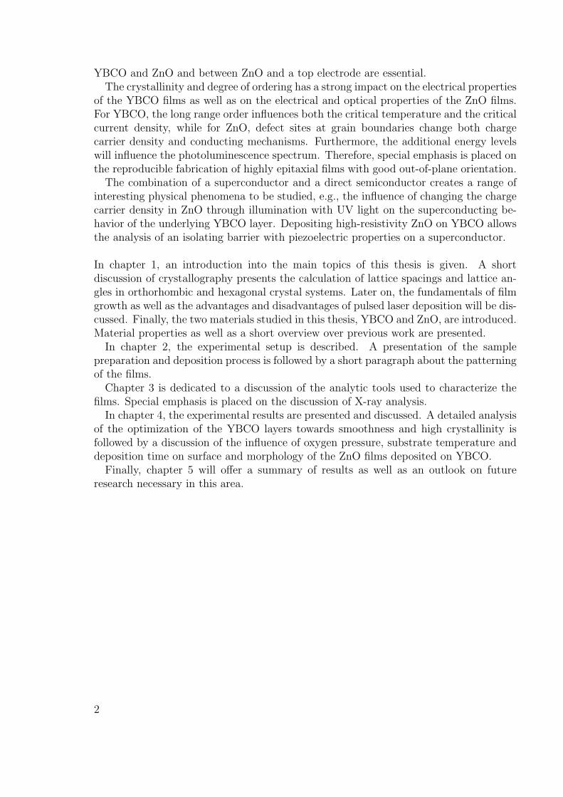
Figure 1.1: Different degrees of ordering: a) low out-of-plane orientation b) high out-of-plane orientation c) low in-plane orientation d) high in-plane orientation.
Polycrystalline material consists of grains which are well-ordered in themselves but havelittle long-range order beyond the boundaries of one grain.
When analyzing polycrystalline films, one differentiates between out-of-plane and in-plane orientation (see fig. 1.1). A film has a high out-of-plane orientation when the c-axisis parallel to the surface normal. In-plane-orientation goes a step further: it measureshow well the a,b-axes of different crystallites are aligned to each other in the plane.
1.2 Thin film growth
For this thesis, I limit myself to the study of thin films grown by pulsed laser deposition(PLD)1. PLD is a simple and versatile technique that allows stoichiometric growth of ahuge variety of composite materials. Some advantages are the simplicity of the process(the small targets required are relatively cheap and easy to fabricate), the precise controlof film thickness, and the possibility to have a high background pressure of a chosenreactive gas (up to a few hundred Pascal).
However, PLD also has two main disadvantages: it is difficult to obtain uniform high-quality films on large substrates due to the narrow angular distribution of the plasmaplume, and it is very difficult to prevent ”splashing”, i.e. the deposition of large particlesor droplets on the newly-grown film.
1The following paragraphs heavily rely on the book ”Pulsed Laser Deposition of thin films” [5] whichpresents a thorough treatment of the development of PLD up to 1993, discussing both the experi-mental details as well as the theoretical models used to describe film growth, even detailing somemodifications of the setup for specific materials.
4

Figure 1.2: Sketch of the PLD setup in on-axis geometry.
For an overview of other methods of thin film growth, the textbook ”Oberflachen- undDunnschicht-Technologie” [6] is recommended, presenting both physical and chemicalvapor deposition techniques and their applications.
1.2.1 Pulsed laser deposition (PLD)
In pulsed laser deposition, nanosecond laser pulses of high fluence (0.5-10 J cm−2) arefocused on a target. The high energy density leads to an explosive vaporization of thetop 50-500 nm, producing a plasma plume of high energy particles (10-200 eV) perpen-dicular to the target surface. Due to the almost instantaneous vaporization, no thermalequilibrium is reached, therefore even composite materials made from elements with verydifferent vapor pressures are uniformly ablated [7].
PLD allows independent control of process parameters like laser fluence, backgroundgas pressure, background gas composition, substrate temperature and substrate positionin respect to the plasma plume. As the initial velocity of the ablated particles is veryhigh (5−35×103 ms−1 [8], [7]), PLD can be performed at gas pressures as high as 1 kPa.
The most commonly used setup of the PLD system is the on-axis geometry, meaningthat the substrate is parallel to the target positioned in the middle of the plasma plume(see fig. 1.2). This setup leads to high deposition rates and a high uniformity of thedeposited films. Furthermore, the incidence of particles perpendicular to the substratesurface can improve the alignment of c-axis growth through an angle-dependent re-sputtering/ablation effect, as Patzig reports [9].
5

Figure 1.3: YBCO film with many droplets (SEM picture, SE mode).
Ablation Process
The ablation process can be described with the sub-surface superheating model [10]: formaterials like YBCO or ZnO, the energy of the incoming short-wavelength laser pulse isabsorbed within the first 10-100 nm. The surface is quickly (4-6 ns) heated to temper-atures around 2000K, leading to sublimation of the topmost layer and accordingly, tocooling of the adjacent regions due to the extracted heat of vaporization. Lower layerscontinue to absorb the laser energy, reaching much higher temperatures, which finallyleads to an explosive vaporization away from the target. The particles therefore have ahigh kinetic energy with a strong forward component which can be described through ashifted Maxwell-Boltzmann distribution on a stream velocity [11].
The ablated material forms a dense plasma layer (n > 1019 cm−3) called Knudsenlayer a few tens of nm above the target surface [7], [12]. In this plasma, the highenergy particles thermalize, leading to plasma temperatures of about 10000K. Whilethe plasma expands, it continues to absorb laser energy through inverse Bremsstrahlungabsorption, leading to an isothermal expansion. When the laser pulse ends, the plasmafinally expands adiabatically, re-transforming thermal into kinetic energy [5].
The angular distribution of the particle flux (and therefore the resulting film thick-nesses d) depend on the angle Θ between substrate and target normal through a cosn(Θ)distribution. The exponent n depends on the energy density of the laser pulse, havingvalues between 1 (insufficient energy density leading to thermal evaporation) and 12 [7].Due to this strong angular dependence, PLD is mainly used for thin film deposition onsmall substrates (1x1 cm2). Larger substrates require rotating holders, a broadened laserplume through use of a focus line instead of a focus spot [13], or multiple laser plumes[14].
Droplets
One major problem of PLD-grown films are droplets - clusters with diameters between100 nm and a few microns which damage the newly-grown film and lead to very rough
6

Figure 1.4: Cones on YBCO target after PLD (OM pictures).
film surfaces (see fig. 1.3).
As seen in previous works, the target surface deteriorates in the PLD process [15].Each shot ablates some material, but there always are surrounding areas which areheated only to their melting point and not to the point of evaporation or even plasma-formation. The melted areas form cone-like structures (see fig. 1.4) of changed compo-sition which change the absorption of the laser pulse and which may explode off thetarget during subsequent laser shots without being vaporized, leading to large droplets(0.5−2 µm) on the substrate [5]. It is therefore necessary to sand the target before eachdeposition to reduce the number of droplets and keep the deposition rate constant [15].
Droplet formation increases when the laser energy is too high, too low or unevenlydistributed: the subsurface layers explode before the upper layers have absorbed enoughenergy to be evenly vaporized in the process. The laser wavelength also has a largeinfluence on droplet formation. In a comparison between infrared, visible and ultra-violet PLD, the UV lasers result in the lowest droplet densities [16].
Over the last 20 years, a variety of experimental methods, including off-axis deposi-tion [17], [18], a mechanical high-speed shutter [19], target modification [12], oscillatingscanning in which the target revolves while being scanned [20], use of a shadow mask[21], [22] and the use of two synchronized laser beams [1] have been used to decrease thedroplet density on YBCO films from the usual 106-107 cm−2 [23] down to 102-105 cm−2.However, all of these methods have their drawbacks or require extensive (and expensive)upgrading of the ordinary PLD setup:
In off-axis geometry, the substrate is held at an angle to the plasma plume particles,sometimes even turned backwards so that only particles scattered to the side or back ofthe plume reach the substrate surface (see fig. 1.5). This reduces the deposition rate andoften leads to non-uniform films as the edge closer to the target grows much faster thanthe one further away; also the stoichiometry can change [24], [25]. In addition, it reducesdroplet density. The droplets are much heavier than the atoms and ions in a plasmaplume, so they get scarcely scattered sideways out of the plume. The non-uniformity canbe overcome by using a rotating substrate holder [18], [26]. Also, the off-axis geometrywith an angle of ∼40 between target and substrate was shown to be of advantage for
7
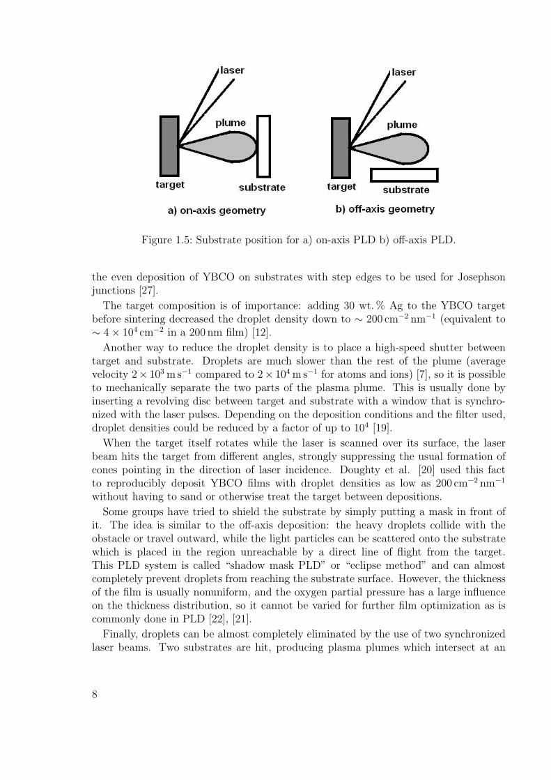
Figure 1.5: Substrate position for a) on-axis PLD b) off-axis PLD.
the even deposition of YBCO on substrates with step edges to be used for Josephsonjunctions [27].
The target composition is of importance: adding 30 wt.% Ag to the YBCO targetbefore sintering decreased the droplet density down to ∼ 200 cm−2 nm−1 (equivalent to∼ 4× 104 cm−2 in a 200 nm film) [12].
Another way to reduce the droplet density is to place a high-speed shutter betweentarget and substrate. Droplets are much slower than the rest of the plume (averagevelocity 2× 10³ ms−1 compared to 2× 10⁴ ms−1 for atoms and ions) [7], so it is possibleto mechanically separate the two parts of the plasma plume. This is usually done byinserting a revolving disc between target and substrate with a window that is synchro-nized with the laser pulses. Depending on the deposition conditions and the filter used,droplet densities could be reduced by a factor of up to 104 [19].
When the target itself rotates while the laser is scanned over its surface, the laserbeam hits the target from different angles, strongly suppressing the usual formation ofcones pointing in the direction of laser incidence. Doughty et al. [20] used this factto reproducibly deposit YBCO films with droplet densities as low as 200 cm−2 nm−1
without having to sand or otherwise treat the target between depositions.
Some groups have tried to shield the substrate by simply putting a mask in front ofit. The idea is similar to the off-axis deposition: the heavy droplets collide with theobstacle or travel outward, while the light particles can be scattered onto the substratewhich is placed in the region unreachable by a direct line of flight from the target.This PLD system is called “shadow mask PLD” or “eclipse method” and can almostcompletely prevent droplets from reaching the substrate surface. However, the thicknessof the film is usually nonuniform, and the oxygen partial pressure has a large influenceon the thickness distribution, so it cannot be varied for further film optimization as iscommonly done in PLD [22], [21].
Finally, droplets can be almost completely eliminated by the use of two synchronizedlaser beams. Two substrates are hit, producing plasma plumes which intersect at an
8
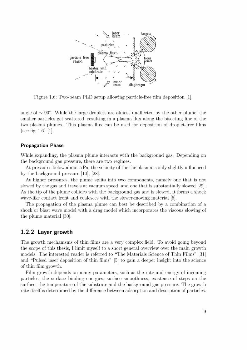
Figure 1.6: Two-beam PLD setup allowing particle-free film deposition [1].
angle of ∼ 90. While the large droplets are almost unaffected by the other plume, thesmaller particles get scattered, resulting in a plasma flux along the bisecting line of thetwo plasma plumes. This plasma flux can be used for deposition of droplet-free films(see fig. 1.6) [1].
Propagation Phase
While expanding, the plasma plume interacts with the background gas. Depending onthe background gas pressure, there are two regimes.
At pressures below about 5Pa, the velocity of the the plasma is only slightly influencedby the background pressure [10], [28].
At higher pressures, the plume splits into two components, namely one that is notslowed by the gas and travels at vacuum speed, and one that is substantially slowed [29].As the tip of the plume collides with the background gas and is slowed, it forms a shockwave-like contact front and coalesces with the slower-moving material [5].
The propagation of the plasma plume can best be described by a combination of ashock or blast wave model with a drag model which incorporates the viscous slowing ofthe plume material [30].
1.2.2 Layer growth
The growth mechanisms of thin films are a very complex field. To avoid going beyondthe scope of this thesis, I limit myself to a short general overview over the main growthmodels. The interested reader is referred to “The Materials Science of Thin Films” [31]and “Pulsed laser deposition of thin films” [5] to gain a deeper insight into the scienceof thin film growth.
Film growth depends on many parameters, such as the rate and energy of incomingparticles, the surface binding energies, surface smoothness, existence of steps on thesurface, the temperature of the substrate and the background gas pressure. The growthrate itself is determined by the difference between adsorption and desorption of particles.
9

Figure 1.7: Thin film growth modes: Volmer-Weber or island growth leads to three-dimensional islands, Frank-van der Merwe or layer growth leads to flattwo-dimensional layers, the intermediate Stranski-Krastanov growth leadsto small clusters on completely filled layers [32].
The ratio between substrate temperature and melting temperature of the film materialis decisive. A higher ratio generally leads to better crystallinity and lower growth rates:as the particles have a higher thermal energy, they move around longer before findingan energetically favorable position, but at the same time they are more prone to desorbbecause of their higher energy.
Three main modes of growth are generally distinguished, named layer or Frank-vander Merwe growth, island or Volmer-Weber growth and Stranski-Krastanov growth (seefig. 1.7).
These modes can be described and explained by simple thermodynamic considerationsabout the free energy of clusters on the surface of a substrate. Taking into account theinterface energies between substrate, vapor and cluster as well as substrate temperatureand supersaturation (the ratio of the pressure of the arriving atoms to the vapor pressureof the deposited material), it is possible to determine whether monolayers or clusterswill form.
Although the above-mentioned growth models describe how films grow dependingon the interaction between substrate and film material as well as thermodynamic pa-rameters, the growth is often strongly influenced by the surface of the substrate itself.Dislocations and steps change local binding energies and offer favorable nucleation sites,leading to either screw dislocations or film growth through the propagation of growthsteps, termed “ledge growth” [33].
Film growth with pulsed laser deposition
In PLD, short plasma plumes lasting 5− 10ms are followed by long periods of hundredsof ms in which no material is deposited. The short phase of very high supersaturationallows the formation of many small clusters which are unstable at lower deposition ratesdue to their small size. In the intermediate period with low arrival rates, the clusterswill therefore begin to dissociate and coalesce into larger, stable clusters in an Oswaldripening step. This reordering on the surface depends strongly on the kinetic energyinfluenced by substrate temperature.
If the second pulse arrives too quickly after the first, there will be no difference to
10

continuous laser deposition as no real dissociation of unstable clusters will have takenplace. In the case of a long intermediate time between pulses, all the clusters willhave reformed into the larger clusters that also would result from a low instantaneousdeposition rate.
The film growth will only be influenced by the splitting into two phases when the timeconstants for the laser are such that the next pulse arrives while the atoms from the firstpulse are still rearranging themselves on the surface, i.e., the laser pulses arrive on thetime scale of the atomic reordering processes.
The time constants can easily be changed as most pulsed lasers allow pulse frequenciesbetween 1 and 100Hz without changing the pulses themselves. Therefore, the effectof different time intervals on film growth has been extensively studied, showing theexpected strong influence and the existence of an optimum interval for deposition of aspecific material [34].
1.3 Superconductivity
In 1911, Heike Kamerlingh Onnes discovered that mercury below 4.2 K has no mea-surable resistance [35]. Later, the Dutch physicist called the observed phenomenonsuperconductivity and received a Nobel prize for his research in this area in 1913. Fur-thermore, it was also discovered that superconductivity could be quenched by a magneticfield. Since superconductors are ideally diamagnetic, they expel any magnetic fields in-side them, a property known as the Meissner -Ochsenfeld effect.
Many elements exhibit superconductivity when cooled below a certain critical temper-ature, TC . Common to all superconductors is the fact that they lose the superconductivestate when either the temperature is raised above TC , or when they are immersed in amagnetic field above the critical field strength HC , or when they carry a current abovethe critical current density jC . These three parameters are directly dependent on eachother as can be seen in fig. 1.8.
Figure 1.8: Critical surface phase diagram of Type I superconductors: the material showssuperconductive behavior if it is closer to the origin than the critical surface[36].
11

Depending on how a superconductor becomes quenched by magnetic fields, it is clas-sified as either Type I or Type II superconductor:
Type I superconductors are ideally diamagnetic, expelling all magnetic field untilthe critical field strength HC is reached, in which case superconductivity breaks downcompletely. In contrast, a Type II superconductor can exist in a mixed state calledShubnikov phase [37], in which small parts of the superconductor are in normal state,allowing some flux to penetrate the material while the rest is still in superconductingstate.
1.4 YBa2Cu3O7−x
The high-temperature superconductor YBa2Cu3O7−x (YBCO) with a transition tem-perature T0
C ∼ 92K was discovered by Wu et al. in 1987 and belongs to the cuprateswith perovskite-like structure. Like all high-temperature superconductors it is of TypeII, with a large London penetration length λL and a short coherence length ξGL.
1.4.1 Crystal structure
YBa2Cu3O7−x is found in tetragonal and orthorhombic phase, depending on oxygenconcentration and temperature (see fig. 1.9). Only the orthorhombic phase, where0 < x < 0.6, shows superconductive behavior, and the transition temperature is highlydependent on the oxygen concentration, showing its maximum of 92K at x∼0.05 [38].
Superconductivity in YBCO, as in most cuprates, takes place in the CuO2-planes(assigned Cu(2) in fig. 1.9): These planes are effectively hole-doped, as some electronsare transferred to the oxygen atoms in the CuO-chains (Cu(1) in fig. 1.9) [39]. As theconducting CuO2-planes are only linked in a,b-direction, it is obvious that YBCO isa highly anisotropic material. The coherence length in a,b-direction is about 5-8 timeslarger than in c-direction, and the London penetration length λL in a,b-direction is aboutfive times smaller than in c-direction [39].
The lattice constants of the completely oxygenated orthorhombic unit cell containing13 atoms at room temperature can be found in table 1.1.
lattice parameters volume number density thermal exp. coeff. at 300 Kmaterial a [A] b [A] c [A] V [A3] n [1022 cm−3] αa,b [10−6 K−1]YBCO 3.820 3.885 11.676 173.3 7.503 10ZnO 3.249 3.249 5.204 54.945 7.28 5
Table 1.1: Material properties of YBCO and ZnO [40], [41], [42], [43].
1.4.2 Growth mechanisms of YBCO thin films
The growth of YBCO thin films on various substrates via PLD has been the focus ofmuch research for the last twenty years. Though the exact parameters vary between
12

Figure 1.9: YBCO phases and phase diagram; T stands for tetragonal, O for the or-thorhombic phases differing in their long-range order [44].
different groups, YBCO films are usually deposited by PLD in the following processparameter ranges [10], [34], [5]:
• oxygen pressure: between 10 and 50Pa,
• temperature: between 650 and 850 C,
• laser energy: between 1 and 4 J cm−2,
• laser repetition rate: between 1 and 30Hz,
• post-deposition oxygenation oxygen pressure: 103 − 105 Pa.
While some groups claim they see proof of Volmer-Weber growth [5], the high densityof relatively flat, terrace-like screw dislocations (∼ 108 cm−2) rather supports anothermodel, where small screw dislocations form at many nucleation sites, followed by atwo-dimensional growth at the screw’s step edges [33].
Chang et al. [34] found pinholes for low repetition rates around 1Hz which theyattribute to extensive nuclei ripening in the intermediate period. Higher repetition ratesof 10-30Hz improve the coalescence and lead to smooth films, while a further increaseof the repetition rate yields films with precipitates, often consisting of Y2O3, YCuO2 orBaCu2O2.
Substrate Material: SrTiO3
SrTiO3 (STO) is a material with perovskite structure which is commonly used as sub-strate for YBCO thin film deposition. Its lattice parameter in a,b-direction (a=b=3.905 A)and the thermal expansion coefficient (α ∼ 11 × 10−6 K−1) are close to that of YBCO,
13

Figure 1.10: ZnO in the hexagonal wurtzite structure [2], [3].
furthermore it is chemically inert and very little diffusion is found between YBCO andSTO [45], [46].
1.5 Zinc oxide (ZnO)
Zinc oxide (ZnO) is a wide band gap (∼ 3.3 eV) semiconductor with a large free excitonbinding energy of about 60meV. ZnO single crystals are therefore transparent, while thepolycrystalline target has a white-yellowish tint. ZnO is easily processed by wet chemicaletching, and comparatively cheap to fabricate. Although ZnO has been known for morethan fifty years, the last decade has seen renewed interest in ZnO as it seems suitablein various active fields of research like UV light emitting diodes (LED), transparentconducting oxides (TCO), surface acoustic wave guides (SAW) and lasing applications[2].
1.5.1 Crystal structure
ZnO forms a wurtzite structure at normal pressure, in which each zinc atom is surroundedby four oxygen atoms at the corner of a tetrahedron and vice versa (see fig. 1.10). Asone basal plane terminates in zinc atoms while the other terminates in oxygen atoms,the (001) and the (001)-planes have different properties and the whole crystal exhibitspolarity along the c-axis. This polarity explains the piezoelectric behavior and influencesmany properties of ZnO, including growth and etching [2].
The lattice constants of the hexagonal unit cell containing 4 atoms at room tempera-ture can be found in table 1.1.
When grown on cubic substrates, it is possible to stabilize ZnO in cubic zinc blende
14

structure, while a pressure of about 10GPa leads to a transition to rocksalt structure.The zinc blende unit cell has a lattice constant of about 4.5 A, while the rocksalt unitcell has a lattice constant of about 4.27 A [2].
1.5.2 Electric properties
Undoped ZnO shows n-type behavior with donor concentration ranging between 1017
and 1021 cm−3. The reason for the high charge concentration is still debated. Originally,the shallow donor levels were attributed to oxygen vacancies and zinc interstitials [2].However, it was found that oxygen vacancies act as deep donors, and that zinc inter-stitials have too high formation energies to account for 1017 cm−3 free charges. It hasbeen suggested that hydrogen is the cause for the low donor levels, a theory which iscorroborated by annealing experiments [47].
Fabricating stable p-doped ZnO has long seemed impossible as the introduction ofacceptors into the ZnO crystal usually resulted in overcompensation and n-type behav-ior, but in the last years several groups have published results which seem relativelyincontrovertible [48]. They also offer explanations why many groups have not succeededin measuring p-type doping: ZnO shows persistent photoconductivity so samples haveto be protected from UV light the days before performing Hall measurements [49].
As mentioned before, the resistivity of ZnO films varies between 10−4 − 109 Ω cm,making ZnO usable both as piezoelectric material, which requires very high resistivity,and TCO, where a very low resistivity is required [2].
1.5.3 Pulsed laser deposition of ZnO
Deposition of ZnO films through PLD has received considerable attention, but individualgroups report very different parameters at which they produced the best films, as canbe seen in table 1.2. Common to all ZnO films is the predominance of c-axis growth onmost substrates. Furthermore, most groups find grain sizes of 10-100 nm, with grain sizeincreasing as substrate temperature or oxygen pressure are increased.
To better understand the growth mechanisms of ZnO film growth, some attention hasbeen given to the study of the plasma plume itself [8], [58].
Through high-speed analysis of the emission lines from the plasma plume resultingfrom ablation of ZnO with a nanosecond UV laser, different ionized states of Zn atomstogether with their velocities could be observed. Usually, strong emissions from Zn+-ionswith a mean kinetic energy of 36-57 eV were found. At higher laser fluences (>4 J cm−2)or femtosecond laser pulses, very fast Zn++-ions were observed, probably fast enough(> 200 eV kinetic energy) to damage the films.
Another feature are slow particles trailing behind the main plume, consisting probablyof Zn atoms which first backscattered from the plasma and then rebounded from thetarget. This interpretation is corroborated by the common observation that the targetsurface changes upon first irradiation, even in the vicinity of the laser focus. The origi-nally insulating yellow ZnO turns into grayish-metallic conducting material – probablya thin layer of Zn [58].
15

group substrate temperature pressure ∆2Θ ∆2ω roughness[C] [Pa] [] [] [nm]
Bae [50] Al2O3 200-600 0.0001 - 67 0.2Beck [43] Al2O3 300-750 0.1-40 0.45-4 0.6 - 24
Fouchet [51] Al2O3 400-750 4 - 27 0.3 - 1.8 20 - 50Kaidashev [52] Al2O3 600-750 0.04 - 1.5 0.06 - 0.12 0.2 - 2
Kim [53] Si 600 0.07 - 70 0.2 - 0.4 4 - 26Klini [8] Si, silica 300-650 0.005 - 0.5 0.2 - 2 1 - 9 1 - 20
Mitra [54] glass 20 1.3 - 130 0.6 - 1.2 20 - 110Ohshima [28] Si, silica, 20-700 0.007 - 27 0.5 - 8
Al2O3
Prasad [55] steel 70-80 10−7 - 0.7 0.5 10Savchuk [56] quartz, 20-550 0.13 - 1300 0.16
Al2O3
Zerdali [57] SiO2 500 0.013 0.28
Table 1.2: Summary of deposition parameters for PLD of ZnO.
Figure 1.11: Sketch of the PLD setup in on-axis geometry.
16

2 Experimental setup: samplepreparation
2.1 Pulsed laser deposition (PLD) setup
The basic setup of the pulsed laser deposition (PLD) System is shown in fig. 1.11.A Lambda Physics LPX3051 KrF excimer Laser with a wavelength of 248 nm was
used. The laser produced pulses with a duration of ∼ 20 ns at a repetition rate of1-10Hz. The energy could be varied between 600 and 1100mJ per pulse.
The laser beam was focused through a lens with 50 cm focal length onto the targetto a focus size of 5 − 7mm2. As the resulting laser intensity was too high for optimaldeposition of YBCO, an optical attenuator was placed in the optical path.
The resulting laser fluence at the target was in the range of 0.7 to 2.6 J cm−2.Three targets (YBCO, ZnO and Au) were mounted on a revolvable target holder, with
the laser beam hitting the target at an angle of about 45. To improve the yield of onetarget, the laser spot was scanned in a rectangular pattern over the whole target surface(see fig. 2.1) with the help of a deflecting mirror controlled by two stepper motors.
As the growth of YBCO thin films requires a homogeneous substrate temperaturearound 750 C, the substrate was attached with conductive silver to a resistive heater.A thermocouple was also attached to the heater. The heating current was controlledwith a Eurotherm 818P temperature control unit that used the measurement from thethermocouple to keep the temperature at a set level.
The control loop kept the temperature as measured with the thermocouple stableto ± 1 C, however, the temperature measured with the thermocouple differed widely(20-30 C) from the temperature of the substrate as determined with a pyrometer. Asthe pyrometer is calibrated to black-body radiation while the substrate is certainly a
Figure 2.1: This laser scan pattern was used to maximize the yield of the target.
17

gray body, this effect is not surprising. Furthermore, the thermocouple is positionedabout 1 cm outside the main heating area of the heater and the thermal contact betweensubstrate and heater varies from sample to sample. For each single deposition I thereforedetermined the substrate temperature with a pyrometer and set the heater control loopaccordingly.
From repeated measurements I determined the reproducibility of the pyrometer to± 5 C. The accuracy of the absolute value is not known, as no suitable calibrationstandard was available. This uncertainty is of relatively little importance for this thesis:for an analysis of the influence of different parameters on film fabrication in this setup itsuffices to have reproducible values on a relative scale, and if a transfer to another setupis wanted, it should be possible to fix this scale to the real temperature scale throughan external calibration measurement.
The PLD was performed in on-axis geometry, with the substrate positioned right infront of the target with a separation of 4 cm between target and substrate.
The deposition chamber was evacuated using a Leybold Turbovac 361 turbomolecularpump with a Leybold Trivac rotary vane pump as backing pump. The minimum pressurereached with this setup was 5 × 10⁻⁵ Pa, measured with a Balzers compact full rangepressure gage.
2.2 Deposition process
The substrates were first polished (rms surface roughness ∼ 1 nm), then cleaned in anultrasonic bath first with acetone, then with isopropyl alcohol, blown dry with nitrogen,and finally wiped clean with acetone-moistened wipes.
The substrates were glued onto the heater with conductive silver paste to ensure uni-form heat transport from heater to substrate and therefore even heating of the substrate.
First, the vacuum recipient was evacuated to less than 3×10⁻⁴ Pa. The turbomolecularpump was then switched off and the oxygen flow was increased until the depositionpressure for YBCO was reached (10-40Pa with rotary vane pump still running). Whilethe substrate was protected by a mask, the target was ablated for a minute (about 10shots per site).
The substrate was heated to the deposition temperature (700-850 C), and the YBCOdeposition was performed. Then, the rotary vane pump was stopped and the oxygenpressure increased to 6×10⁴ Pa. The temperature was decreased down to room temper-ature at a rate of 2400 C/hour.
In the case of subsequent ZnO deposition, the vacuum recipient was then evacuatedwith the rotary vane pump down to 0.3Pa before the oxygen flow was increased to reachthe desired pressure (1-10Pa with rotary vane pump still running). The depositiontemperatures were lower than the ones for YBCO (200-550 C), but else the depositionprocess and parameters were the same.
I am aware of the fact that the changing pumping speeds of the rotary vane pump atdifferent pressures together with the positioning of the pressure meter to the side of theoxygen inlet decrease the accuracy and validity of the pressure measurements. However,
18
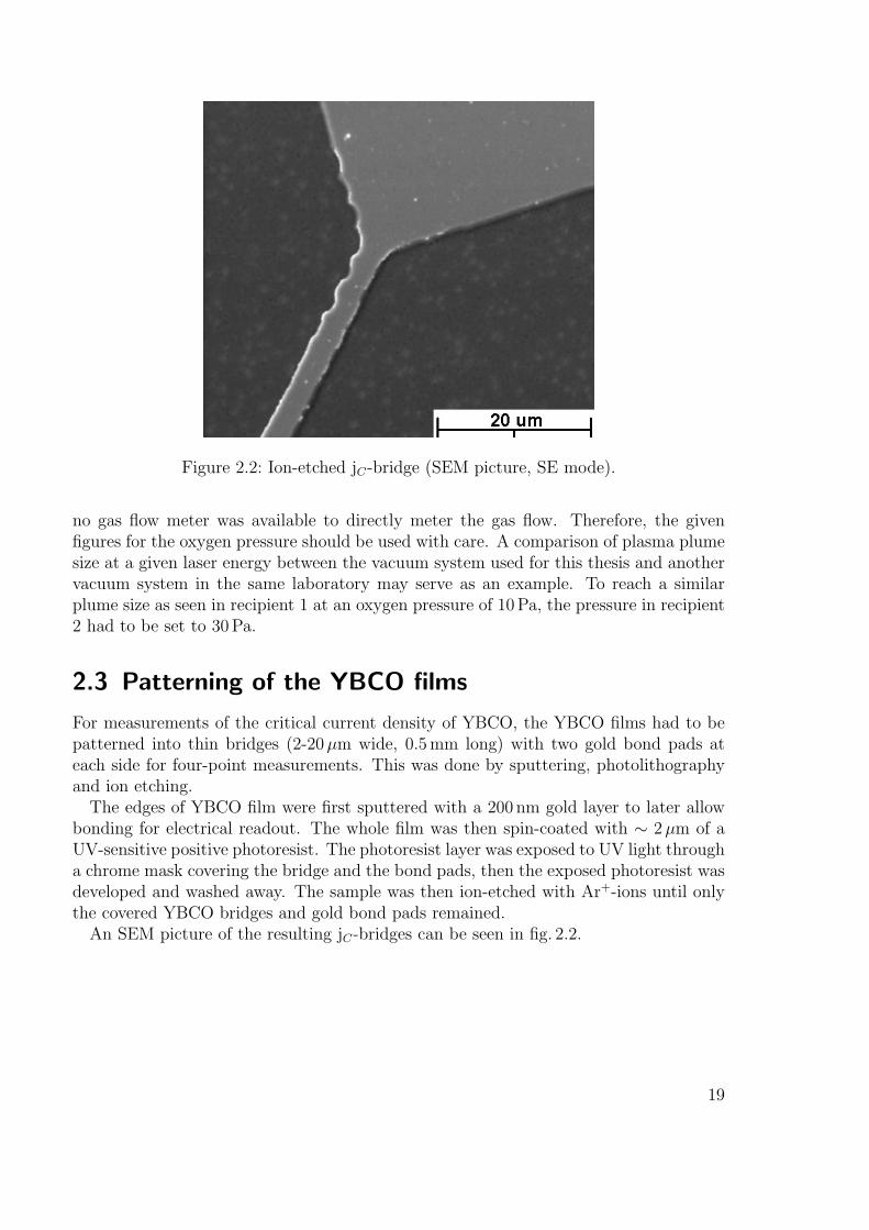
Figure 2.2: Ion-etched jC-bridge (SEM picture, SE mode).
no gas flow meter was available to directly meter the gas flow. Therefore, the givenfigures for the oxygen pressure should be used with care. A comparison of plasma plumesize at a given laser energy between the vacuum system used for this thesis and anothervacuum system in the same laboratory may serve as an example. To reach a similarplume size as seen in recipient 1 at an oxygen pressure of 10Pa, the pressure in recipient2 had to be set to 30Pa.
2.3 Patterning of the YBCO films
For measurements of the critical current density of YBCO, the YBCO films had to bepatterned into thin bridges (2-20µm wide, 0.5mm long) with two gold bond pads ateach side for four-point measurements. This was done by sputtering, photolithographyand ion etching.
The edges of YBCO film were first sputtered with a 200 nm gold layer to later allowbonding for electrical readout. The whole film was then spin-coated with ∼ 2µm of aUV-sensitive positive photoresist. The photoresist layer was exposed to UV light througha chrome mask covering the bridge and the bond pads, then the exposed photoresist wasdeveloped and washed away. The sample was then ion-etched with Ar+-ions until onlythe covered YBCO bridges and gold bond pads remained.
An SEM picture of the resulting jC-bridges can be seen in fig. 2.2.
19

3 Analytical methods
To determine the properties of the fabricated layers, several analytical methods wereused. The properties and the respective methods are shown in table 3.1 and detailedbelow.
Property Methodsurface morphology Atomic Force Microscopy (AFM)
Scanning Electron Microscopy (SEM)layer thickness Dektak profilometer
Rutherford Backscattering Spectroscopy (RBS)crystallinity X-Ray Diffraction (XRD)
superconducting properties:T0
C R(T) measurementsjC I-V characteristics
Table 3.1: Analyzed properties and the respective analytical method
3.1 Profilometry
The thickness of the YBCO layers was determined with the help of a Dektak 3030profilometer. Parts of the YBCO film were wet etched with 3% hydrochloric acid (HCl)to create a sharp step edge between film and substrate. Although the resolution of theprofilometer was stated as 0.1 nm, the film thicknesses could only be measured to anaccuracy of ±15 nm due to film roughness and rounding effects at the step edge.
3.2 Rutherford backscattering spectroscopy (RBS)
Rutherford Backscattering Spectroscopy (RBS) relies on the wide-angle scattering oflight ions (usually He+ or H+) with high kinetic energies in the range of 100 keV to someMeV on target atoms inside a solid.
An ion beam is focused onto a target and the amount and energy of the backscatteredions are measured by a detector. The ions mostly undergo elastic scattering with theatoms in the sample, so the energy of the backscattered ion is directly dependent on themass of the nucleus. Therefore, elements on the surface of a sample can be identified bythe energy of backscattered ions.
20
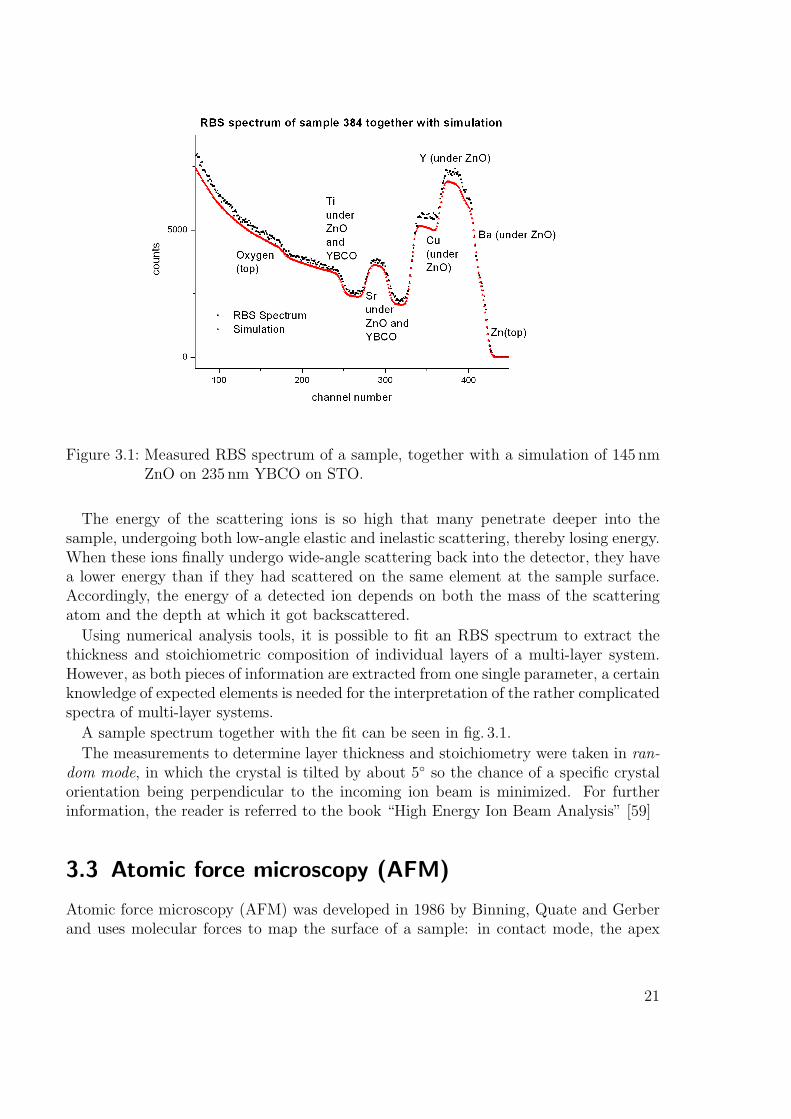
Figure 3.1: Measured RBS spectrum of a sample, together with a simulation of 145 nmZnO on 235 nm YBCO on STO.
The energy of the scattering ions is so high that many penetrate deeper into thesample, undergoing both low-angle elastic and inelastic scattering, thereby losing energy.When these ions finally undergo wide-angle scattering back into the detector, they havea lower energy than if they had scattered on the same element at the sample surface.Accordingly, the energy of a detected ion depends on both the mass of the scatteringatom and the depth at which it got backscattered.
Using numerical analysis tools, it is possible to fit an RBS spectrum to extract thethickness and stoichiometric composition of individual layers of a multi-layer system.However, as both pieces of information are extracted from one single parameter, a certainknowledge of expected elements is needed for the interpretation of the rather complicatedspectra of multi-layer systems.
A sample spectrum together with the fit can be seen in fig. 3.1.
The measurements to determine layer thickness and stoichiometry were taken in ran-dom mode, in which the crystal is tilted by about 5 so the chance of a specific crystalorientation being perpendicular to the incoming ion beam is minimized. For furtherinformation, the reader is referred to the book “High Energy Ion Beam Analysis” [59]
3.3 Atomic force microscopy (AFM)
Atomic force microscopy (AFM) was developed in 1986 by Binning, Quate and Gerberand uses molecular forces to map the surface of a sample: in contact mode, the apex
21
atom of a tip is scanned over a surface and experiences a repulsive force when comingtoo close to the surface atoms. As the tip is mounted on a flexible cantilever, the forceleads to a deflection of the cantilever which is monitored with a laser. A feedback-loop moves the cantilever with the help of piezoelectric ceramics so that the tip alwaysexperiences the same repulsive force from the surface. In principle, an AFM can reacha sub-nm lateral and even better vertical resolution. Further information can be foundin the book “Surface analyis with STM and AFM: experimental and theoretical aspectsof image analysis” [60].
The AFM pictures shown in this thesis were taken with a Veritekt AFM by Zeiss,reaching a resolution of ∼ 5 nm in lateral and ∼ 0.5 nm in vertical direction. All root-mean-square (rms) roughnesses were determined over an area of 5× 5 µm2.
3.4 Scanning electron microscopy (SEM)
Scanning electron microscopy (SEM) uses the scattering of high-energy electrons on asample to reveal topographical and material-sensitive information about the surface.Electrons are accelerated to kinetic energies of 10-30 keV and focused through a seriesof electromagnetic lenses onto the target. The fast electrons impinge on the surfaceand undergo elastic and inelastic scattering in the first fewnm, either creating cascadesof secondary electrons with much lower kinetic energy or backscattering from a nu-cleus, thereby retaining their energy but changing the direction. The electron beam isscanned over the sample and either the low-energy secondary electrons (SE mode) orthe high-energy backscattered electrons (BSE mode) are measured by a detector. Whilethe amount of secondary electrons depends mainly on the topography, the amount ofbackscattered electrons depends strongly on the element: the heavier the nucleus, thehigher the number of backscattered electrons. Further information can be found in thebook “Physical principles of electron microscopy” [61].
The SEM pictures shown in this thesis were taken with a TESLA BS 343 SEM,reaching a lateral resolution of ∼ 100 nm.
3.5 R(T)-measurements
To determine the critical temperature T0C of the YBCO thin film, simple four-point
probe resistance measurements were taken. The four contacts made from copper wirewere mechanically pressed onto the YBCO surface, while the back of the substratetouched a large brass body which acted as a thermal mass. A platinum thermocouple(Pt100) was fixed to this brass body to monitor the temperature. A DC current of100µA was supplied by a constant current source while the voltage drop on the othertwo electrodes was measured with a Prema 5000 Digital Multimeter. The sample wasslowly lowered (about 20K per hour in the region of 77.4-100K) by a stepper motor intoa dewar with liquid nitrogen while the resistance and the temperature were registeredby a computer. A sample R(T)-curve can be seen in fig. 3.2.
22

Figure 3.2: Sample R(T)-measurement of an YBCO film, showing T0C , TC(90%) (tem-
perature at which the resistance dropped by 90% of the linear fit of thenormal resistance), TC(10%) and ∆TC=TC(10%)-TC(90%).
The definition of the critical temperature TC of the transition from normal to su-perconducting state varies in literature [37]. In this work, the following terms are used(see fig. 3.2 for visualization): T0
C (temperature at which the resistance dropped to zerowithin the measurement accuracy of ∆R ∼ 0.05 Ω), TC(90%) (temperature at which theresistance dropped by 90% of the linear fit of the normal resistance), TC(10%) (temper-ature at which the resistance dropped by 10% of the linear fit of the normal resistance)and ∆TC=TC(10%)-TC(90%).
To judge the reliability of the measured values and to estimate the influence of the rateof temperature change, measurements were taken both while lowering and while raisingthe sample, thereby decreasing and increasing the temperature. Although differences inT0
C of up to 4K were found at higher rates of temperature change, no difference wasnoted for measurements taken with the above-mentioned rate of ∼20K per hour.
The accuracy of the determination of T0C depends strongly on the R(T)-curve. While
some samples showed a very abrupt transition in which the maximum uncertainty wouldbe ±0.25K, other samples showed a strong tail in the transition which increases theuncertainty to ±1.5K. The same holds for the accuracy of ∆TC : the determination ofTC(10%) is difficult as the upper shoulder of the R(T) curve tends to be quite round.
Note that four-point probe resistance measurements show zero resistance as soon asthere is a superconducting path between the contacts. For information about largerareas of the layer other methods like magnetic susceptibility measurements are moresuitable.
23
3.6 jC-measurements
The critical current density jC was determined by measuring I-V characteristics of struc-tured micro-bridges (0.5mm long and 2-20µm wide) at 77.4K with a Keithley sourcemeasure unit. The critical current was determined by the 10µV criterion. The main un-certainties arise from the film thickness (known to ± 10%) and the bridge width (knownto ± 0.5µm).
3.7 X-ray diffraction (XRD)
For the last century, X-Ray Diffraction (XRD) methods have been the most importantand powerful tool for the analysis of crystallography. XRD is based on the fact that thewavelengths of X-rays are in the order of magnitude of the separation of single atoms ormolecules in solids, i.e., 0.05-5 nm. Therefore, X-rays undergo diffraction in an orderedsolid, leading to reflexes according to Bragg’s law [4]:
nλ = 2d sin Θ, (3.1)
where n is the order of the reflex, λ the X-ray wavelength, d the lattice plane spacing,and Θ the angle between incident X-ray and lattice plane.
It is possible to extract information about lattice spacing, crystallite size, out-of-planeorientation and in-plane orientation from the X-ray diffraction data, as will be explainedlater in more detail.
3.7.1 X-ray diffractometer
The set-up used for my experiments was a Seifert Bragg-Brentano-diffractometer (seefig. 3.3) with a four-circle goniometer for sample positioning. The four-circle goniometerallows independent control of 2Θ, ω, χ and φ (see fig. 3.4 for a visualization of theseangles).
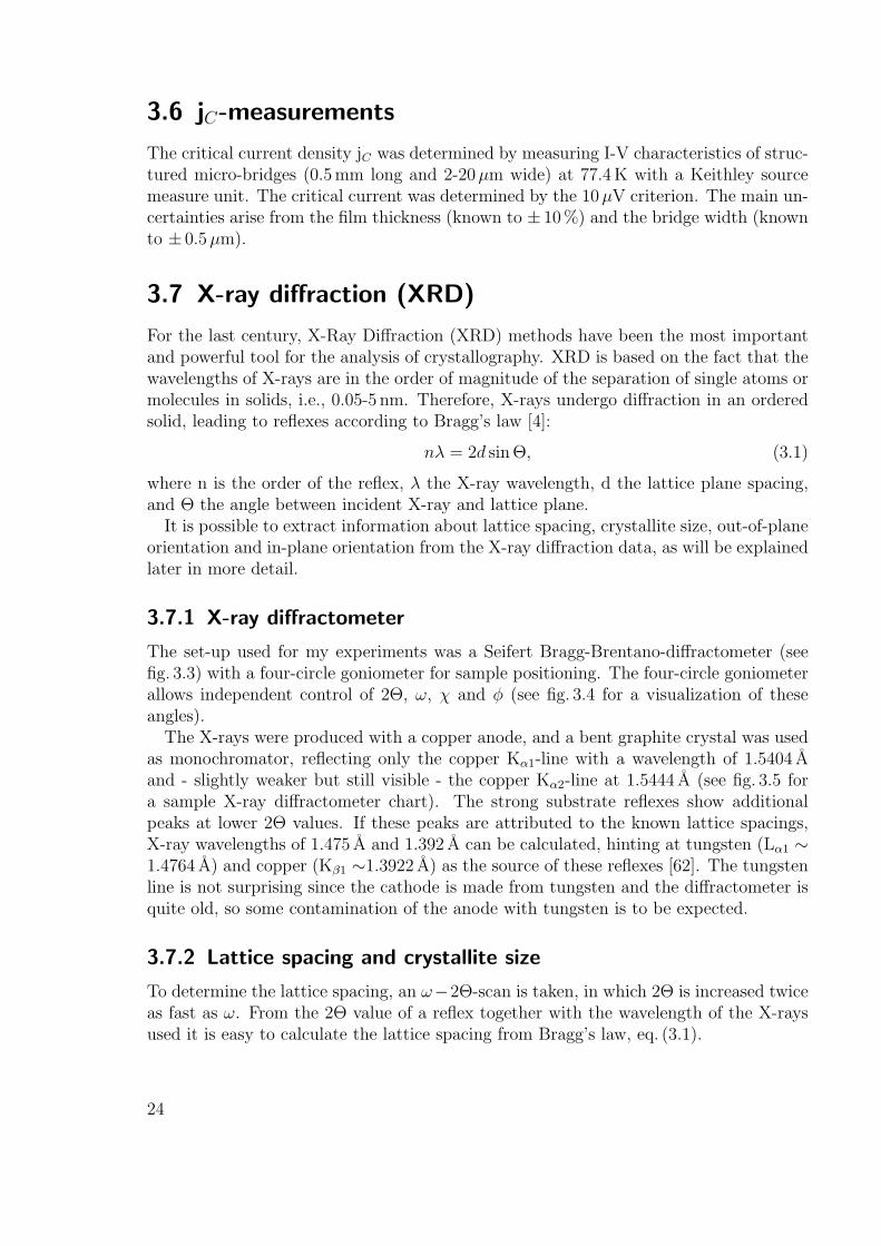
The X-rays were produced with a copper anode, and a bent graphite crystal was usedas monochromator, reflecting only the copper Kα1-line with a wavelength of 1.5404 Aand - slightly weaker but still visible - the copper Kα2-line at 1.5444 A (see fig. 3.5 fora sample X-ray diffractometer chart). The strong substrate reflexes show additionalpeaks at lower 2Θ values. If these peaks are attributed to the known lattice spacings,X-ray wavelengths of 1.475 A and 1.392 A can be calculated, hinting at tungsten (Lα1 ∼1.4764 A) and copper (Kβ1 ∼1.3922 A) as the source of these reflexes [62]. The tungstenline is not surprising since the cathode is made from tungsten and the diffractometer isquite old, so some contamination of the anode with tungsten is to be expected.
3.7.2 Lattice spacing and crystallite size
To determine the lattice spacing, an ω−2Θ-scan is taken, in which 2Θ is increased twiceas fast as ω. From the 2Θ value of a reflex together with the wavelength of the X-raysused it is easy to calculate the lattice spacing from Bragg’s law, eq. (3.1).
24

Figure 3.3: Sketch of the Bragg-Brentano X-ray diffractometer with a four-circle go-niometer.
Figure 3.4: The angles accessible by the four-circle goniometer: 2Θ, ω, χ and φ.
25
Figure 3.5: XRD chart, showing the multiple reflexes from the STO002 peak due to dif-ferent X-ray lines.
To compensate for a possible systematic offset of the measured 2Θ values, I alsomeasured 2Θ of the (001) and (002) peak of the STO substrate. Compared with thecalculated lattice spacing values for STO the 2Θ values are 0.18 too large, so I subtracted0.18 from all further 2Θ measurements.
An infinite perfect crystal would result in a perfectly narrow reflex, however realcrystallites are finite, smearing out the Bragg reflex. It is therefore possible to calculatethe crystallite size from the full width at half maximum (FWHM) of a peak in the ω−2Θscan, ∆2Θ, according to the Debye-Scherrer-Formula [4]:
< L >=Kλ
B1/2 cos Θ, (3.2)
where L is the crystallite column length perpendicular to the surface averaged over thefilm volume, K the Scherrer constant (depending on the unit cell geometry, typicallybetween 0.8 and 1.4) [63], B1/2 the FWHM of the peak in radians and Θ the Bragg anglefor the peak.
Beside the crystallite size there are other reasons for peak broadening like the above-mentioned diffractometer broadening or strain broadening, so this formula should onlybe used to give the order of magnitude of the crystallite size, not exact values.
As the Scherrer constant is determined by the geometry of the crystallites which isusually unknown, it is commonly set as unity. Consequently, the values calculated inthis work should be treated with caution, and an uncertainty of ±50% is estimated.
26
3.7.3 Crystal orientation
The out-of-plane orientation can be determined through an ω rocking curve. 2Θ is fixedto the value of the analyzed reflex while ω is varied. The FWHM of the rocking curve,∆ω, is a common measure for how well the crystallites are oriented with respect to thesubstrate normal.
A misalignment of the out-of-plane orientation of two consecutive layers can be foundby first measuring the offset between ω and Θ of one layer and then comparing it withthe offset of the second layer.
To determine the in-plane orientation, it is necessary to do an asymmetric scan to plotthe reflex of a lattice plane which is not parallel to the substrate. To this end, the anglebetween lattice plane normal and substrate normal has to be calculated according toeq. (1.3) for orthorhombic crystals and eq. (1.4) for hexagonal crystals. χ is set to thisangle, 2Θ and ω are set to their respective values, and φ is scanned from 0 to 360.
The FWHM values of the φ-scan is a common measure for the in-plane orientation.As it is much easier to overlook an asymmetric peak due to the additional degrees offreedom, all φ-scans were recorded with the largest aperture.
Asymmetric scans can also be used to detect the growth orientation, e.g., a-axis growthin YBCO. Usually, a-axis growth would be detectable through a simple ω-2Θ-scan, butthe strongest a-axis peak at 47.49 is completely overshadowed by the STO substratepeak at 46.6 which has wide flanks. Therefore, it is necessary to use a peak like YBCO102
which is not parallel to the c-axis (offset by 56), fix ω and 2Θ to the corresponding val-ues and do φ-scans at ξ=56 and ξ=90-56=34. If a peak appears at ξ=56, the filmhas c-axis oriented grains, if a peak appears at ξ=34 there are also a-axis orientedgrains.
3.7.4 Evaluation of the XRD data
The XRD data results from the convolution of a Gaussian resulting from “diffractometerbroadening”, mostly due to the aperture size, with the actual curve stemming from thediffraction process, which in itself may have the form of a Gaussian (e.g. due to limitedcrystallite size) or a Lorentzian, the natural line shape of any exponentially dampenedtransition.
As the natural line width is smaller than either the broadening due to aperture size ordue to crystallite size, the resulting curve “final” is here presumed to be the convolutionof two Gaussians “initial” and “broadening” with individual full width at half maximum(FWHM) ∆initial and ∆broadening, leading to a combined FWHM ∆final according to
∆final =√
∆2broadening + ∆2
initial. (3.3)
The initial line width can therefore easily be calculated if the diffractometer broadeningis known. Due to the quadratic terms, this correction is only necessary for FWHM
27
values smaller than three times the diffractometer broadening; for larger initial FWHMvalues the broadening influence is below 10%.
To evaluate the XRD data, the program “Analyze” supplied with the diffractometerwas used. The ω-2Θ-scans were fitted with multiple Gaussian curves, yielding positionand full width at half maximum (FWHM) for each peak. The rocking curves, whichhave the form of a Voigt curve1, were fitted with a Pseudo-Voigt, which is just a linearcombination of a Lorentzian with a Gaussian.
3.7.5 Accuracy of the measurements
The accuracy of the measurements is determined by several factors.For the position, accuracy of the 2Θ measurement and the positioning of the sample
are of importance. The specifications of the X-ray diffractometer give the accuracy ofthe angles as ±0.005. The influence of sample position on 2Θ can easily be seen infig. 3.3: if the sample is behind the middle of the circle, the actual angle of diffractionis larger than the one calculated from the position of source and detector. The sampleposition was determined through a contact gage to ±0.02mm, from which an uncertaintyof ±0.004 can be calculated for a 2Θ-range of 30 to 50.
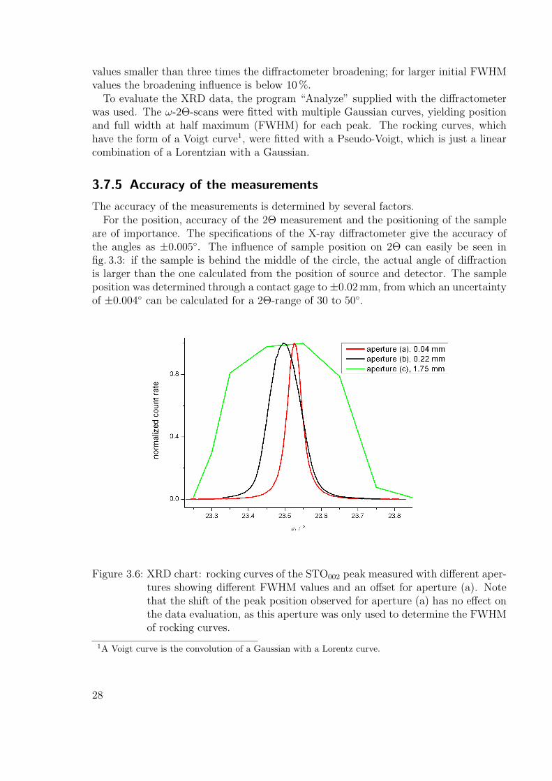
Figure 3.6: XRD chart: rocking curves of the STO002 peak measured with different aper-tures showing different FWHM values and an offset for aperture (a). Notethat the shift of the peak position observed for aperture (a) has no effect onthe data evaluation, as this aperture was only used to determine the FWHMof rocking curves.
1A Voigt curve is the convolution of a Gaussian with a Lorentz curve.
28
However, the peak position is determined through a fit of the XRD data with aGaussian. The accuracy of the fit itself is limited by the aperture size and amount ofstatistical noise. A smaller aperture improves the accuracy, but also reduces the countrate, increasing statistical noise for samples with low crystallinity.
The minimal FWHM measurable with different apertures was experimentally deter-mined by measuring the rocking curve of the STO single crystalline substrate which isexpected to have a natural line width far below the resolution capability of this diffrac-tometer. The resulting FWHM are 0.045 for aperture (a) (0.04mm), 0.09 for aperture(b) (0.22mm), and 0.4 for aperture (c) (1.75mm) in fig. 3.6). For this thesis, most scanswere taken with aperture (b), only for measurements of rocking curves with FWHM be-low 0.14 aperture (a) was used, and for asymmetric scans (see chapter 3.7.3) aperture(c) was used.
The accuracy is strongly diminished by the fact that the peak itself often does nothave the form of a Gaussian or even a Pseudo-Voigt, but rather has a shoulder to theright side which might be the result from the Cu Kα2-reflex. Therefore, an uncertaintyof ±15% of the FWHM of a fit is assumed both for position and FWHM of a peak. Asthis uncertainty is usually larger than the uncertainties arising from sample positioningand 2Θ-measurement, these ±15% of FWHM are taken as the final uncertainty for allXRD values.
29

4 Experimental results and discussion
In this thesis, a separation of the presentation of results and their discussion was over-ruled in favor of a joint approach, treating each property like variation of film surface independence of deposition parameters in itself, before continuing with the next aspect,e.g., crystallinity.
For the fabrication of thin film multilayer epitaxial structures, both surface and mor-phology of the individual layers are of utmost importance.
If the surface of a layer is too rough or covered by droplets, the next layer will notevenly cover it. When the surface roughness is in the order of magnitude of the filmthickness (50-100 nm), the electrical properties will be unpredictable in a multilayersystem, and the same is true for a droplet with a size of 0.5-2µm: it is immediatelyobvious that a droplet in the active area of a device may lead to an electrical short-circuit, rendering the multilayer structure useless.
The crystal structure needs to be well-oriented, else epitaxial growth of consecutivelayers becomes impossible.
Therefore, the layers were optimized towards minimum surface roughness, minimumdroplet density and best out-of-plane orientation. The YBCO layers need to be improvedtowards better superconducting properties, but in this thesis this task was subordinateto the achievement of multilayer structures and awaits completion by later graduatestudents.
4.1 Changes to the pulsed laser deposition system
4.1.1 Target treatment
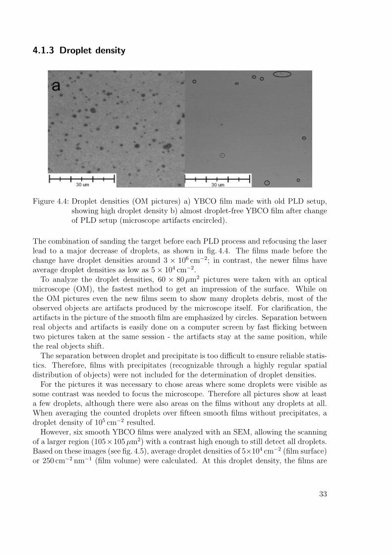
As described in chapter 1.2.1, the target surface deteriorates in the PLD process. Infig. 4.1, pictures of the target surface before and after deposition are shown.
To reduce the number of droplets and prevent a change in laser absorption throughcone formation, the target was sanded after each single deposition, thereby returningthe surface to its virgin state. As the composition of the top layer of the target is quicklychanged by the first laser shots, the target was ablated for a minute (about 10 shots persite) before deposition to ensure a relatively uniform target composition over the courseof one deposition.
30

Figure 4.1: Target surface (OM pictures): a) YBCO before deposition b) YBCO afterdeposition c) ZnO before deposition d) ZnO after deposition.
4.1.2 Laser focus
To determine the size of the laser focus, thermal paper was fastened to the target andhit by a single laser pulse.
As seen in fig. 4.2a, the main maximum becomes oval and secondary maxima appearwhen the laser beam is focused to its maximum intensity. Furthermore, the laser inten-sity seems to vary over the area of the main maximum, although both the spatial andthe energy density resolution of the thermal paper are not sufficient for a quantitativeanalysis.
Observation of the target shows melting in the close vicinity of the main maximum(see fig 4.3). As explained above, melting of the target without evaporation increasesdroplet formation, so it was necessary to change the optical path and the laser focus.
The laser beam leaving the laser has a cross-section area of 1.6× 3.2 cm2 and consistsof one strong beam and two secondary beams which propagate at a small angle to theprimary beam, leading to the two secondary maxima seen in fig. 4.2a. To remove thesesecondary beams, the optical path was extended to about three meters by insertingtwo high-reflectivity mirrors. The secondary beams now passed to the side of the finalmirror, so only the main beam was focused by the lens onto the substrate. This lead toa decreased energy, but it improved the beam profile.
31

Figure 4.2: Photographs of laser focus at target site: a) old laser focus on thermal paperb) new laser focus on thermal paper.
Figure 4.3: Photos of YBCO target after deposition: melting outside the directly ablatedareas [14].
The optimal focus was then determined to be 1 cm behind the focal point (focal lengthof the lens: 50 cm). The resulting focus has a rectangular form with relatively sharpedges (see fig. 4.2b). As the target is at a 45 angle to the incoming laser beam, the sizeof the rectangle varies between (5.25 ± 0.2)mm2 and (7.05 ± 0.2)mm2, depending onwhether the target is hit at the top or the bottom. The average focus size of 6.15mm2
was taken to calculate laser fluence values, and the change of focus size by ±0.9mm2
(relative variation of 15%) together with a laser stability of ∼ 5% leads to a variation ofthe laser fluence of ∼ 20%.
The laser fluences used for film deposition were (1.8±0.4) J cm−2, (1.05±0.21) J cm−2
and (0.93±0.19) J cm−2.As most of the better films were made at a laser fluence close to 1 J cm−2 which is
often stated as a lower bound for YBCO PLD, the fluence variation due to the scanningof the target may actually have an influence on the YBCO films. However, the geometryof the PLD setup makes it impossible to overcome this angle-dependant resizing of thefocus: to hit the target at the steeper angle necessary for a more uniform focus size, thelaser beam would have to pass through the substrate heater which has to be positionedright in front of the target for on-axis PLD.
32
4.1.3 Droplet density
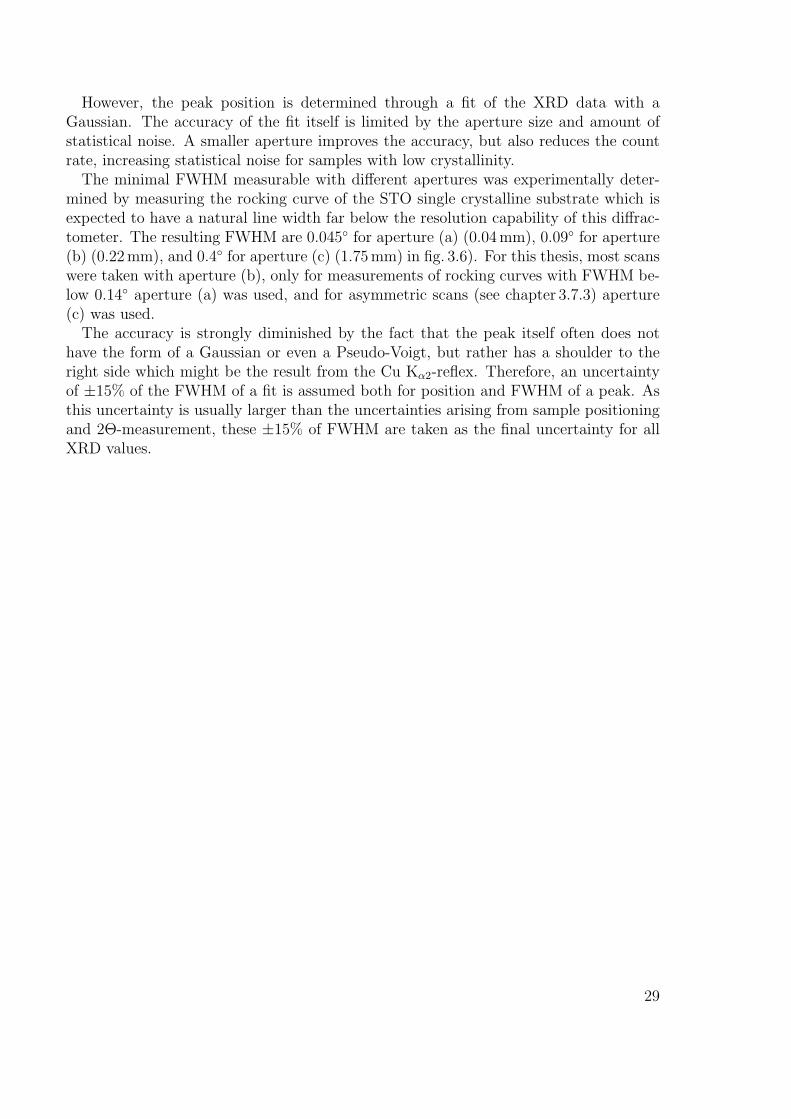
Figure 4.4: Droplet densities (OM pictures) a) YBCO film made with old PLD setup,showing high droplet density b) almost droplet-free YBCO film after changeof PLD setup (microscope artifacts encircled).
The combination of sanding the target before each PLD process and refocusing the laserlead to a major decrease of droplets, as shown in fig. 4.4. The films made before thechange have droplet densities around 3 × 106 cm−2; in contrast, the newer films haveaverage droplet densities as low as 5× 104 cm−2.
To analyze the droplet densities, 60 × 80 µm2 pictures were taken with an opticalmicroscope (OM), the fastest method to get an impression of the surface. While onthe OM pictures even the new films seem to show many droplets debris, most of theobserved objects are artifacts produced by the microscope itself. For clarification, theartifacts in the picture of the smooth film are emphasized by circles. Separation betweenreal objects and artifacts is easily done on a computer screen by fast flicking betweentwo pictures taken at the same session - the artifacts stay at the same position, whilethe real objects shift.
The separation between droplet and precipitate is too difficult to ensure reliable statis-tics. Therefore, films with precipitates (recognizable through a highly regular spatialdistribution of objects) were not included for the determination of droplet densities.
For the pictures it was necessary to chose areas where some droplets were visible assome contrast was needed to focus the microscope. Therefore all pictures show at leasta few droplets, although there were also areas on the films without any droplets at all.When averaging the counted droplets over fifteen smooth films without precipitates, adroplet density of 105 cm−2 resulted.
However, six smooth YBCO films were analyzed with an SEM, allowing the scanningof a larger region (105×105 µm2) with a contrast high enough to still detect all droplets.Based on these images (see fig. 4.5), average droplet densities of 5×104 cm−2 (film surface)or 250 cm−2 nm−1 (film volume) were calculated. At this droplet density, the films are
33

Figure 4.5: Droplet densities (SEM pictures, SE mode) a) YBCO film made with oldPLD setup, showing high droplet density b) almost droplet-free YBCO filmafter change of PLD setup.
well-suited for further use in multi-layer processing: the chance of finding a droplet inthe active area of a micro-electronic device (e.g., a SQUID) which usually have sizes of10 - 100µm2 is reduced to less than 1:20.
When comparing this result with other YBCO films produced by on-axis PLD havingaverage droplet densities of 106-107 cm−2 [23], [26], or with the works of Schmauder etal. [27] who did off-axis-deposition with the same PLD setup and found their lowestdroplet density of 3× 105 cm−2 at an angle of 60 between target and substrate1, I wasable to significantly reduce the number of droplets.
Other groups have used different methods to lower their droplet densities even further,as was discussed in chapter 1.2.1. However, if the setup cannot be changed for eitherfinancial or technical reasons, the techniques used in this thesis seem a feasible optionto greatly reduce droplet densities to the point where resulting films can be used formicroelectronic devices without having too many droplet short-circuits.
4.1.4 Heater
To simplify the deposition process and reduce contamination by conductive silver paste,I experimented with a new clamping heater design.
Usually, the substrates are glued to the heater with conductive silver, making theexchange of substrates a lengthy process: the old substrate is carefully removed witha blade (thin substrates may break when glued too tightly to the heater), the heatersurface is sanded to remove the old conductive silver paste, new silver is applied, thesubstrate is pressed into the silver, the heater is slowly heated over 30min first to 110Cand then to 300C to let the solvent slowly evaporate, because faster heating leads to
1At 0 degree (on-axis) they report a droplet density of 1.5× 106 cm−2.
34

bubble formation and therefore uneven heat transfer between heater and the back sideof the substrate.
Furthermore, the back of the substrate is covered in conductive silver paste afterdeposition. When the substrate is cleaned in an ultrasonic acetone bath for furtherprocessing steps, small silver particles are often swept onto the YBCO surface, possiblyleading to short-circuits in multi-layer systems [64].
The new clamping system was designed to facilitate the exchange of substrates andavoid the use of conductive silver paste: using a mask which covered only the outerhalf millimeter of the substrate, the back of the substrate was pressed to the smoothedsurface of the heater to form a good thermal contact between heater and substrate.While it was possible to achieve sufficiently high substrate temperatures in this way, twomain difficulties appeared which I could not be overcome:
The thermal conduction was highly dependent on the background pressure. Withfixed temperature control circuit set on 840 C, a change of pressure from 1 to 40Palead to an increase in substrate temperature (as measured with a pyrometer) from 790to 840 C. Therefore any change in pressure (as necessary for subsequent deposition ofYBCO and ZnO) necessitated new calibration of the temperature control unit, whichfor the ZnO deposition was very difficult due to the low deposition temperatures of200− 550 C that are far outside the pyrometer’s working range of 780− 1600 C.
Figure 4.6: Clamping heater (thermocouple measuring 790 C for both photos): a) beforedeposition, the substrate glows brightly and b) after deposition, where thefilm is relatively dark.
Furthermore, the deposition process changed the radiation of the substrate, while notinfluencing the characteristic of the thermocouple. This lead to a decrease in substratetemperature from ∼ 800 C to less than 760 C over the course of the deposition process(see fig. 4.6). As the pyrometer itself cannot be used for automated temperature controlbecause it is based on the comparative capacity of the human eye, no temperature controlcircuit could be designed which actually monitored the substrate temperature and notthe heater temperature.
For these reasons, I settled for attaching the substrates with conducting silver.
At the moment, experiments with a newly-acquired infrared-sensitive sensor to con-tinually monitor the substrate temperature during the deposition process are conducted.
35

The hope is to overcome the problem of the varying thermal conduction between heater,substrate and environment.
4.2 Optimization of the YBCO layer
As the main goal of my thesis is the deposition of ZnO in YBCO/ZnO multilayer systems,I first had to optimize the YBCO deposition process for the fabrication of YBCO layersusable for the subsequent deposition of ZnO.
Having in mind the use of such multilayer systems for microelectronics, the attributesI tried to achieve in the films are, in descending order of importance:
• a smooth surface with no precipitates which might pierce an insulating top layer,
• very high crystallographic quality to allow epitaxial growth of subsequent layers,
• sufficient superconducting properties.
I was able to resort to the knowledge of another member of our work group whostudies YBCO/STO/Au-multilayer systems to get started on the deposition of YBCOfilms [45]. However, the differences in the setup of our deposition chambers and thehigh sensitivity of the YBCO film quality on the deposition parameters forced me tofabricate extended series of YBCO samples to find the working point in which I couldreliably produce smooth YBCO thin films of sufficient crystallographic quality2.
4.2.1 Layer thickness of YBCO films
As the profilometer method for the determination of thickness is a destructive method,it was the last measurement taken for the samples. Therefore, variation of parameterscould also lead to different thicknesses which could not be compensated for.
The first samples produced at fluences around 1.8 J cm−2 and pressures between 20-40Pa had 20 minutes deposition time and showed thicknesses between 400 and 900 nm.
The later samples produced at fluences around 1 J cm−2, a partial oxygen pressure of10Pa and 7 minutes deposition time showed thicknesses between 160 and 235 nm.
4.2.2 Surface of YBCO films
The quality of the surface was diminished by two features: either the surface itself wouldhave many tiny troughs, leading to a uniformly rough surface, or precipitates wouldform, rendering the growth of further continuous films impossible. Optical microscopy,SEM and AFM pictures of a rough surface can be seen on sample 322 in fig. 4.7, whileprecipitates are clearly visible on the optical and SEM pictures of sample 372 in fig. 4.8.
2The ZnO deposition happened in situ, therefore there was no possibility to check if the YBCO layerhad the desired quality before depositing ZnO. As I was going to analyze the influence of the ZnOdeposition process on the YBCO, I needed high reproducibility of the YBCO films.
36
Figure 4.7: YBCO films: rough surface of sample 322: a) OM picture b) SEM picture,SE mode c) AFM scan with rms roughness of 38 nm.
As there is little contrast in the SEM picture taken in BSE mode, the precipitatesprobably have a stoichiometry similar to the surrounding film. In contrast, in a film inwhich the cooling to room temperature was performed three times slower than for theother films, precipitates formed which are of a different composition than the surroundingfilm (see fig. 4.9).
To show the influence of different growth temperatures, the quality of the surface,determined through an optical microscope, was rated on a scale from 0-5, 0 being verysmooth and 5 very rough. As I needed to get a general impression of the influenceof different parameters on the surface quality, taking AFM scans of every sample wasunfeasible and the categorization by eye was sufficient to find a temperature range inwhich it was possible to get very smooth surfaces (see fig. 4.11): although there are somevariations, only films produced at substrate temperatures between 740 C and 775 Cshow the possibility of being both very smooth and free of precipitates. In addition, aclear influence of laser fluence can also be observed in fig. 4.11, where out of six samplesproduced at 0.93 J cm−2 only one sample is not in category 0.
To further underline the influence of laser fluence on the surface roughness, this de-pendence is plotted in fig. 4.12. There was always a relatively smooth and a relativelyrough sample for a given fluence and it is difficult to determine a trend from the fewpoints visible in the diagram, so I decided to also show the average of the roughnessesof all samples produced at this fluence. The data points for average roughness show aclear trend to smoother surfaces at lower laser fluences.
To further quantify these results, a few samples were analyzed by AFM measurements.The AFM measurements validated the earlier categorization: The rms roughness mea-sured over an area of 5x5µm2 for the sample in category 3 and the one in category 2 is50 nm and 28 nm, respectively; the four samples in category zero from which I took AFMmeasurements have rms roughnesses between 2.5 and 6 nm and are therefore sufficientlysmooth for multi-layer fabrication.
37

Figure 4.8: YBCO films: precipitates on sample 372: a) OM picture b) SEM picture,SE mode c) SEM picture, BSE mode: weak contrast is a sign of similarcomposition to the film itself.
Figure 4.9: YBCO films: precipitates on surface of sample 369: a) OM picture b) SEMpicture, SE mode c) SEM picture, BSE mode: strong contrast is a sign ofdifferent composition than the film.
38
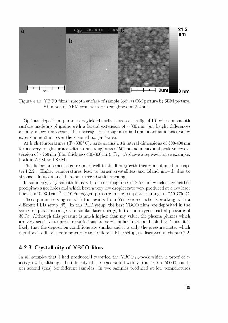
Figure 4.10: YBCO films: smooth surface of sample 366: a) OM picture b) SEM picture,SE mode c) AFM scan with rms roughness of 2.2 nm.
Optimal deposition parameters yielded surfaces as seen in fig. 4.10, where a smoothsurface made up of grains with a lateral extension of ∼300 nm, but height differencesof only a few nm occur. The average rms roughness is 4 nm, maximum peak-valleyextension is 21 nm over the scanned 5x5µm2-area.
At high temperatures (T∼830 C), large grains with lateral dimensions of 300-400 nmform a very rough surface with an rms roughness of 50 nm and a maximal peak-valley ex-tension of ∼260 nm (film thickness 400-800 nm). Fig. 4.7 shows a representative example,both in AFM and SEM.
This behavior seems to correspond well to the film growth theory mentioned in chap-ter 1.2.2. Higher temperatures lead to larger crystallites and island growth due tostronger diffusion and therefore more Oswald ripening.
In summary, very smooth films with an rms roughness of 2.5-6 nm which show neitherprecipitates nor holes and which have a very low droplet rate were produced at a low laserfluence of 0.93 J cm−2 at 10Pa oxygen pressure in the temperature range of 750-775 C.
These parameters agree with the results from Veit Grosse, who is working with adifferent PLD setup [45]. In this PLD setup, the best YBCO films are deposited in thesame temperature range at a similar laser energy, but at an oxygen partial pressure of30Pa. Although this pressure is much higher than my value, the plasma plumes whichare very sensitive to pressure variations are very similar in size and coloring. Thus, it islikely that the deposition conditions are similar and it is only the pressure meter whichmonitors a different parameter due to a different PLD setup, as discussed in chapter 2.2.
4.2.3 Crystallinity of YBCO films
In all samples that I had produced I recorded the YBCO005-peak which is proof of c-axis growth, although the intensity of the peak varied widely from 100 to 50000 countsper second (cps) for different samples. In two samples produced at low temperatures
39
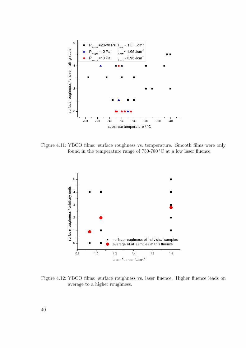
Figure 4.11: YBCO films: surface roughness vs. temperature. Smooth films were onlyfound in the temperature range of 750-780 C at a low laser fluence.
Figure 4.12: YBCO films: surface roughness vs. laser fluence. Higher fluence leads onaverage to a higher roughness.
40

(∼705 C), I detected weak signs of a-axis growth through an asymmetric scan, as wasexplained in chapter 3.7.3.
Lattice spacing
When plotting the corrected 2Θ-value of the YBCO005 peak for samples deposited atdifferent temperatures and oxygen partial pressures (see fig. 4.13), two results appear:for samples produced at 1.8 J cm−2 and 10Pa oxygen pressure the 2Θ value increases athigher temperatures, from ∼38.2 at 705 C to ∼38.46 at 840 C, and samples producedat a lower fluence and a lower oxygen partial pressure have on average higher 2Θ values,the majority showing 2Θ ∼38.45 at 750-770 C.
Larger 2Θ-values result from a smaller lattice spacing: 38.2 equals a c-axis parameterof 11.77 A, 38.46 equals 11.69 A. Fully oxygenated bulk YBCO has a c-axis parameterof ∼11.68 A.
The change of c-axis length could be attributed to a combination of three effects.First, the film formation depends strongly on the mobility and diffusion of particles onthe surface. If the substrate temperature is increased, the arriving particles have moreenergy to find energetically favorable positions; if the incoming particle flux is decreasedthrough a decrease of laser fluence, the individual particles have more time to formregular unit cells. Accordingly, both changes should lead to better crystallinity, which Iexperimentally verified for lattice spacing and out-of-plane orientation.
Second, strain from the lattice mismatch between YBCO and STO will influence thecell parameters of the film. The thicker a film grows, the more it relaxes into its normalconfiguration. Therefore a sample series with strongly varying thickness whith all otherparameters kept unchanged and an analysis of the 2Θ-shift compared to film thicknesscould reveal the influence of lattice mismatch.
Finally, YBa2Cu3O7−x cell parameters are directly influenced by the amount of oxygen(7 − x) contained. Several research groups have extracted the oxygen content frommeasurements of c-axis lengths. Most groups find a linear dependence in quite a largerange (oxygen content 6.5-6.95), but the exact formula to calculate the oxygen contentfrom the c-axis parameter varies from group to group, depending on different samplepreparation procedures [65], [66], [67], [68]. From a graph by Ye et al. [68] in which theyplot c-axis parameter over oxygen content of thin films produced by molecular beamepitaxy, I extracted the following formula used to caluclate the oxygen content (7− x):
7− x = (13.0476− c)× 5.161. (4.1)
Although I did not independently determine the oxygen content of my samples toconfirm or disprove this dependence for my samples, I observed an influence of lat-tice spacing on superconducting behavior, which makes such a link very probable, seechapter 4.2.5 for further details.
Out-of-plane orientation
To evaluate the out-of-plane orientation of YBCO, the FWHM of the rocking curve ofthe YBCO005-peak (from now on called ”rocking curve FWHM”) is used in almost all
41
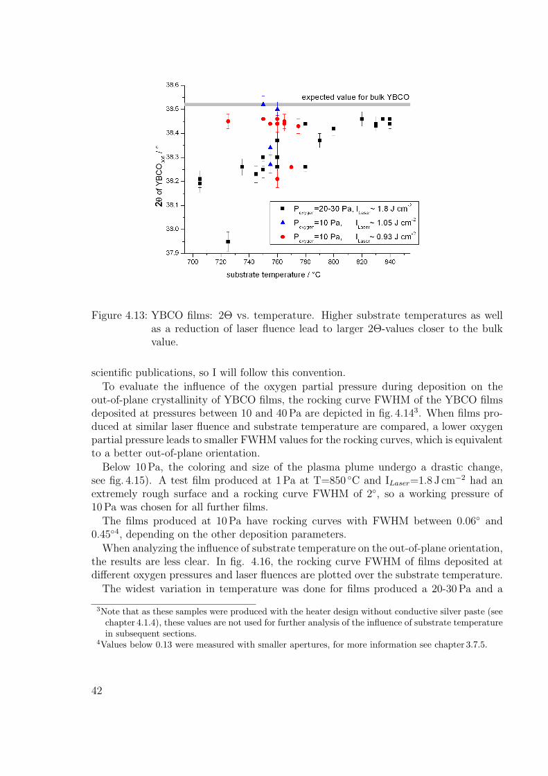
Figure 4.13: YBCO films: 2Θ vs. temperature. Higher substrate temperatures as wellas a reduction of laser fluence lead to larger 2Θ-values closer to the bulkvalue.
scientific publications, so I will follow this convention.
To evaluate the influence of the oxygen partial pressure during deposition on theout-of-plane crystallinity of YBCO films, the rocking curve FWHM of the YBCO filmsdeposited at pressures between 10 and 40Pa are depicted in fig. 4.143. When films pro-duced at similar laser fluence and substrate temperature are compared, a lower oxygenpartial pressure leads to smaller FWHM values for the rocking curves, which is equivalentto a better out-of-plane orientation.
Below 10Pa, the coloring and size of the plasma plume undergo a drastic change,see fig. 4.15). A test film produced at 1Pa at T=850 C and ILaser=1.8 J cm−2 had anextremely rough surface and a rocking curve FWHM of 2, so a working pressure of10Pa was chosen for all further films.
The films produced at 10Pa have rocking curves with FWHM between 0.06 and0.454, depending on the other deposition parameters.
When analyzing the influence of substrate temperature on the out-of-plane orientation,the results are less clear. In fig. 4.16, the rocking curve FWHM of films deposited atdifferent oxygen pressures and laser fluences are plotted over the substrate temperature.
The widest variation in temperature was done for films produced a 20-30Pa and a
3Note that as these samples were produced with the heater design without conductive silver paste (seechapter 4.1.4), these values are not used for further analysis of the influence of substrate temperaturein subsequent sections.
4Values below 0.13 were measured with smaller apertures, for more information see chapter 3.7.5.
42

Figure 4.14: YBCO films: rocking curve vs. pressure. Higher oxygen pressure leads toworse rocking curves.
Figure 4.15: Photos of plasma plume from YBCO target: a) 10Pa oxygen pressure b)1Pa oxygen pressure.
laser fluence ILaser=1.8 J cm−2 (black dots in fig. 4.16). At high temperatures between830 and 840 C, the FWHM values of the six films show only small variations between 0.1and 0.18, so all films produced at these parameters have a very good out-of-plane crys-tallinity. When decreasing the temperature, FWHM increases until reaching a maximumof ∼0.47 at 790 C. Between 700 and 790 C, different samples show a large variation ofFWHM values between 0.27 and 0.47 without a clear correlation to the temperature,although average FWHM values seem to slightly decrease with decreasing temperatures.
The samples produced at a lower oxygen pressure of 10Pa all lie in the range of 725-775 C, where no direct influence of the temperature on the rocking curve FWHM wasobserved. Instead, the laser fluence has a large impact on the out-of-plane crystallinity:at a laser fluence ILaser=1.05 J cm−2, the films have rocking curve FWHM values of 0.21-
43

Figure 4.16: YBCO films: rocking curve vs. temperature. Average rocking curve FWHMvalues around 0.4. FWHM values decrease strongly when increasing sub-strate temperatures to ∼ 830K or when reducing the laser fluence at tem-peratures around 760 C.
0.45. A decrease of laser fluence down to ILaser=0.93 J cm−2 reduces the FWHM to therange of 0.06 - 0.41, with all but one sample having a FWHM of less than 0.2.
In summary, the films show good crystallinity, having rocking curve FWHM valuesof less than 0.5. Optimal conditions were found to be T∼ 760 C, Poxygen=10Pa,ILaser=0.93 J cm−2: Most samples produced with these parameters have a 2Θ-value of38.45 ± 0.03 and rocking curve FWHM values between 0.06 and 0.14 as comparedto ∼ 0.8 before the optimization process, a sign of good epitaxial growth.
4.2.4 Superconducting properties of YBCO films
The films show widely varying critical temperatures T0C for the transition into supercon-
ducting state between 78 and 88.5K, as shown in fig. 4.17.At 20-30Pa oxygen pressure, a plateau at substrate temperatures above 780 C is
observable with T0C values between 84 and 85.5K. At lower temperatures, fluctuation
between samples increases while T0C values decrease as low as 77.5K.
While a reduction of oxygen partial pressure down to 10Pa has relatively little effect,a further reduction of laser fluence down to 0.93 J cm−2 leads to an increase of T0
C valuesup to 88.2K. Although this transition temperature is still below the optimum transitiontemperature of 92K, it is far enough away from 77K to allow stable operation at liquidnitrogen temperature.
44

Figure 4.17: YBCO films: critical temperature vs. substrate temperature. Average T0C ∼
84K, a reduction of laser fluence increases T0C to ∼ 86K, a reduction of
substrate temperature below 750 C strongly reduces T0C .
Similar results are found for the width of the transition to superconducting state. Asthe substrate temperature is lowered from 840 to 705 C, ∆TC rises from a reproducible∼0.9K to wildly fluctuating values as high as ∼8K for samples produced at 20-30Pa and1.8 J cm−2 (see fig. 4.18). At a lower laser fluence of 0.93 J cm−2 and an oxygen pressureof 10Pa, four out of six samples showed ∆TC ≤1K.
One sample was patterned as described in section 2.3 and jC at 77.4K in self-field wasdetermined to jC = (3.2± 0.6)× 105 Acm−2.
In summary, the films show a strong dependence of superconducting properties uponthe deposition parameters. At the parameters determined earlier (T∼ 760 C, Poxygen=10Pa,ILaser=0.93 J cm−2) moderate superconducting behavior was found: most films showT0
C ∼87K, ∆TC ∼1K and jC was determined from one sample to jC = (3.2 ± 0.6) ×105 Acm−2.
It should be recalled that the films were optimized towards a smooth surface. Thefilms show no precipitates and almost no droplets. Usually these objects help the filmto relax strain from lattice mismatch and restore perfect stoichiometry through theexpulsion of excess material. Furthermore, they act as pinning centers for flux vortices,thereby increasing jC . Therefore, the rather moderate superconducting behavior mayvery well be a direct result of the film surface optimization.
45
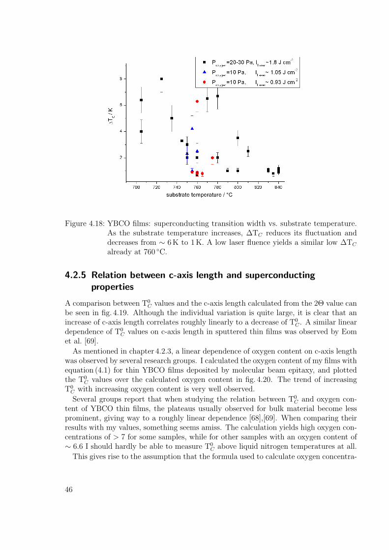
Figure 4.18: YBCO films: superconducting transition width vs. substrate temperature.As the substrate temperature increases, ∆TC reduces its fluctuation anddecreases from ∼ 6 K to 1K. A low laser fluence yields a similar low ∆TC
already at 760 C.
4.2.5 Relation between c-axis length and superconductingproperties
A comparison between T0C values and the c-axis length calculated from the 2Θ value can
be seen in fig. 4.19. Although the individual variation is quite large, it is clear that anincrease of c-axis length correlates roughly linearly to a decrease of T0
C . A similar lineardependence of T0
C values on c-axis length in sputtered thin films was observed by Eomet al. [69].
As mentioned in chapter 4.2.3, a linear dependence of oxygen content on c-axis lengthwas observed by several research groups. I calculated the oxygen content of my films withequation (4.1) for thin YBCO films deposited by molecular beam epitaxy, and plottedthe T0
C values over the calculated oxygen content in fig. 4.20. The trend of increasingT0
C with increasing oxygen content is very well observed.
Several groups report that when studying the relation between T0C and oxygen con-
tent of YBCO thin films, the plateaus usually observed for bulk material become lessprominent, giving way to a roughly linear dependence [68],[69]. When comparing theirresults with my values, something seems amiss. The calculation yields high oxygen con-centrations of > 7 for some samples, while for other samples with an oxygen content of∼ 6.6 I should hardly be able to measure T0
C above liquid nitrogen temperatures at all.
This gives rise to the assumption that the formula used to calculate oxygen concentra-
46

Figure 4.19: YBCO films: critical temperature vs. c-axis length. T0C decreases roughly
linearly with c-axis length.
Figure 4.20: YBCO films: critical temperature vs. oxygen content calculated from c-axislength. A roughly linear dependence is observable, but the absolute valuesdo not fit literature values.
47

tion is not appropriate for my samples. A spread of oxygen content of 0.47 (from 6.58 to7.05) should yield a larger spread of T0
C values than the one observed. For a new math-ematical formulation of the relation between c-axis length and oxygen content for mysamples, it would be necessary to perform other measurements like Raman spectroscopy[67], [70] or IR reflectance and transmittance measurements [71] to directly determinethe oxygen concentration of a few chosen samples.
In summary, a roughly linear dependence of T0C on c-axis length was found. The
exact relations between c-axis length, oxygen content and T0C could not be reproduced
with formulas from literature. The scope of this thesis did not allow the collection of asufficient amount of data to form the basis for a new mathematical description.
4.3 Analysis of the ZnO layer
After the deposition conditions for the YBCO layer were optimized, ZnO films weredeposited in situ on the YBCO film for 3, 7 and 20 minutes at 1 or 10Pa oxygen pressures,at temperatures between 200 and 500 C and at a fixed laser fluence of 2.0 J cm−25.
4.3.1 General remarks
Film thicknesses as measured with RBS were 920-1020 nm for 20min deposition time,220-370 nm for 7min deposition time and 120-180 nm for 3min deposition time.
For films deposited at 1Pa oxygen pressure, the plasma plume was much smaller andmore focused than the plume at 10Pa (see fig. 4.21). Most ZnO films deposited at1Pa show a lateral inhomogeneity which probably can be attributed to this focusedplasma plume. The composition and velocity of the particle flux depends strongly onwhether the inner part or the bright periphery of the plume touches the sample. Thebroad plume at 10Pa has a much larger center which almost always covers the whole
5The high laser fluence was chosen because most other research groups have produced good resultswith similar fluences.
Figure 4.21: Photos of plasma plume from ZnO: a) 1Pa oxygen pressure b) 10Pa oxygenpressure.
48

Figure 4.22: ZnO films: surface of sample 362: a) SEM picture, BSE mode b) SEMpicture, SE mode.
Figure 4.23: ZnO films: surface of sample 380: a) OM picture, upper part, lots of pre-cipitates b) OM picture, middle part, smooth surface.
5x10mm2 substrate, so the exact positioning of substrate to target is not as critical asfor the 1Pa plume.
4.3.2 Surface of the ZnO layer
The ZnO surface of most samples is relatively smooth, with an rms roughness of about6 nm6. From SEM pictures with backscattered electrons it can be deduced that thesurface composition is uniform (see fig. 4.22).
Droplet densities are comparable to those measured for the YBCO base layer, so theZnO deposition process seems to add almost no new droplets.
The upper part (when glued to the heater) of the surface of some samples shows lotsof precipitates (see fig. 4.23). As the middle part was always free of precipitates, theseareas were used for AFM analysis of the surface. AFM pictures of chosen samples canbe seen in fig. 4.25.
Relatively little influence of substrate temperature on the surface roughness couldbe detected. Except for two samples with deposition times of 20min and substratetemperatures above 350 C with rms roughnesses of 29 and 32 nm, all samples show anrms roughness between 4 and 8 nm (see fig. 4.24).
6The base YBCO layers have a surface roughness of 2.5-6 nm.
49

Figure 4.24: ZnO films: surface roughness vs. substrate temperature. Most films aresmooth, only films deposited for 20 min at high temperatures show astrongly increased roughness.
However, the surface morphology changes, as can be seen in fig. 4.25. Comparedto the samples produced at T ≤ 350 C and 1Pa which show crystallites with a sizeof 40-70 nm which sometimes cluster together to ∼200 nm large agglomerations, thesamples produced at a higher oxygen pressure of 10Pa show larger crystallites of 100-150 nm which seem to be spread more evenly. This agrees well with findings by othergroups: below ∼ 15Pa, increasing oxygen pressure increases crystallite size [54], [51].
At high temperatures (400-500 C), the sample deposited at 1Pa for 3min shows crys-tallites with a lateral size of 50-130 nm. Upon increasing the deposition time, the smallcrystallites seem to coalesce and continue to grow into very large clusters of ∼300 nmsize with little internal structure visible.
In summary, very smooth films were deposited. Except for the films deposited above350 C for 20min, all films showed smooth surfaces with rms roughness of 4-8 nm. Giventhat the YBCO films used as base layers had themselves an rms roughness of 2.5-6 nm,these values are excellent, and even in comparison to literature values of films depositedon lattice-matched polished substrates, they are still good.
50

Figure 4.25: ZnO films: AFM pictures of chosen sample.
51

Figure 4.26: XRD chart: ω-2Θ-scan of sample with ZnO on YBCO on STO.
4.3.3 Crystallinity of the ZnO layer
In all samples I detected the ZnO002-peak at 2Θ ∼34.3 which is proof of c-axis growth,although the intensity of the peak varied widely between samples, from 50 to 30000counts per second with the same measurement setup. For a sample XRD chart, seefig. 4.26.
In a few samples I also found some a-axis growth as there was a peak at 2Θ ∼31.6
which coincides well with the ZnO100-peak at 31.8. This peak was always smaller thanthe c-axis peak by a factor of 3-10.
Lattice spacing and crystallite size
When plotting the corrected 2Θ-value of the ZnO002 peak for samples deposited at 1Paoxygen pressure at different temperatures (see fig. 4.27), no clear relation is apparent,although a general trend is that higher temperatures lead to increasing 2Θ values. Onesample at 200 C showed 2Θ ∼ 33.7 while at 500 C several samples had 2Θ ∼ 34.3.
The samples produced at a higher oxygen partial pressure of 10Pa show larger 2Θvalues with only a tiny increase from 34.28 at 200 C to 34.4 at 500 C.
These 2Θ-values result from the following lattice spacings: 33.7 equals a c-axis pa-rameter of 5.31 A, 34.4 equals 5.21 A. As bulk ZnO has a c-axis parameter of 5.204 A,the ZnO films are stretched in c-axis direction, but higher temperatures and higheroxygen pressures lead to a decrease of c-axis length close to the bulk value.
Ohshima et al. [28] observed similar behavior for the deposition of ZnO on Si andcorning glass at comparable temperatures and pressures, although their 2Θ values vary
52

Figure 4.27: ZnO films: 2Θ of ZnO001 vs. substrate temperature. Increase of substratetemperature as well as increase of oxygen pressure lead to higher 2Θ values(closer to the bulk value).
between 34.34 and 34.55. This difference in absolute length might be due to thedifferent substrate, although it seems improbable that the ZnO layer would not relaxto normal lattice parameters in a 150-350 nm thick film. Ohshima et al. try to explainthe change in c-axis with either a difference in oxygen content or a difference in thermalexpansion coefficient between film and substrate, as they use SiO2 with an αab half thatof ZnO. As the films deposited on YBCO show the same behavior of decreased c-axislength for higher substrate temperatures despite the αab of YBCO and STO being twicethat of ZnO, the influence of the thermal expansion coefficient seems minimal.
Using the Debye-Scherrer equation (see eq. (3.2)), I calculated the ZnO crystallite sizesfrom the ω−2Θ-scan FWHM values corrected for diffractometer broadening according toeq. (3.3) and plotted them in fig. 4.28. Note that although I present error bars calculatedfrom the FWHM of the ω− 2Θ-scan, there may be a much larger error due to unknowngeometry factors7, therefore the sizes should not be taken as exact values but rathershow trends for changing parameters.
Upon increasing the pressure from 1 to 10Pa, the films deposited for 7min show twiceor three times the crystallite size. Furthermore, a steady increase of crystallite sizefor increasing substrate temperature is visible for all deposition parameters. A similarincrease of crystallite size with temperature was also found by Park et al. [73].
In contrast to the surface analysis by AFM, which showed that a longer deposition
7For further information, see chapter 3.7.2 or a more detailed discussion in [72].
53
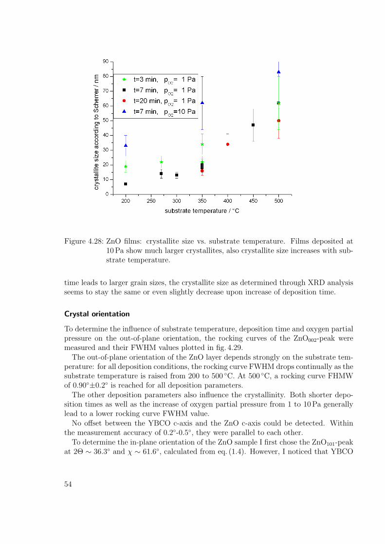
Figure 4.28: ZnO films: crystallite size vs. substrate temperature. Films deposited at10Pa show much larger crystallites, also crystallite size increases with sub-strate temperature.
time leads to larger grain sizes, the crystallite size as determined through XRD analysisseems to stay the same or even slightly decrease upon increase of deposition time.
Crystal orientation
To determine the influence of substrate temperature, deposition time and oxygen partialpressure on the out-of-plane orientation, the rocking curves of the ZnO002-peak weremeasured and their FWHM values plotted in fig. 4.29.
The out-of-plane orientation of the ZnO layer depends strongly on the substrate tem-perature: for all deposition conditions, the rocking curve FWHM drops continually as thesubstrate temperature is raised from 200 to 500 C. At 500 C, a rocking curve FHMWof 0.90±0.2 is reached for all deposition parameters.
The other deposition parameters also influence the crystallinity. Both shorter depo-sition times as well as the increase of oxygen partial pressure from 1 to 10Pa generallylead to a lower rocking curve FWHM value.
No offset between the YBCO c-axis and the ZnO c-axis could be detected. Withinthe measurement accuracy of 0.2-0.5, they were parallel to each other.
To determine the in-plane orientation of the ZnO sample I first chose the ZnO101-peakat 2Θ ∼ 36.3 and χ ∼ 61.6, calculated from eq. (1.4). However, I noticed that YBCO
54

Figure 4.29: ZnO films: Rocking curve vs. substrate temperature. A roughly lineardecrease of rocking curve FHMW with increasing substrate temperature isobserved. Increasing the oxygen pressure also leads to better out-of-planeorientation.
has a peak at similar angles (2Θ ∼ 36.3 and χ ∼ 64.9), the tail of which sometimesinterferes with the measurement of the ZnO peaks due to the large apertures I had touse. I therefore shifted to the ZnO103-peak at 2Θ ∼ 62.9 and χ ∼ 31.6 which has onlyhalf the intensity of the ZnO101-peak.
A φ-scan at these angles showed a 12-fold symmetry (see fig. 4.30), as was expected:when positioning a hexagon on a square, a rotation by 30 leaves the situation unchangedas can be seen in fig. 4.32. The ZnO103 peaks are shifted by 15 in relation to the YBCO102
peaks.
I determined the FHWM values of the φ-scan and plotted them over the rocking curveFWHM values in fig. 4.31. A linear dependence is clearly visible, so at least for the growthon YBCO, the in-plane-orientation of ZnO seems directly connected to the out-of-planeorientation. Therefore it should suffice to determine the rocking curve FWHM in furtherparameter variations of ZnO films.
Fouchet et al. [51] find a similar strong in-plane orientation when depositing ZnO on(001)-Al2O3, while other groups like Zerdali et al. [57] or Wang et al. [74] find no in-plane orientation at all when depositing ZnO on amorphous SiO2. The YBCO sublayerseems to improve the in-plane orientation of the ZnO film compared to a deposition onamorphous material. This is surprising, as an optical analysis of the positioning of thehexagonal ZnO structure on the orthorhombic YBCO structure does not immediatelyreveal that a 15 offset is energetically favorable to other positions (see fig. 4.32).
55
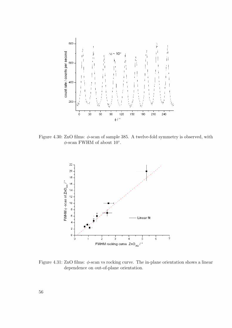
Figure 4.30: ZnO films: φ-scan of sample 385. A twelve-fold symmetry is observed, withφ-scan FWHM of about 10.
Figure 4.31: ZnO films: φ-scan vs rocking curve. The in-plane orientation shows a lineardependence on out-of-plane orientation.
56

Figure 4.32: Observed positioning of the hexagonal ZnO lattice on the orthorhombicYBCO lattice: a) 15 offset between ZnO and YBCO b) rotating theZnO by 30 leaves the situation unchanged, therefore a 12-fold symmetryis observed in the φ-scan.
4.3.4 YBCO degradation due to ZnO deposition
To determine whether the YBCO layer is degraded by the ZnO deposition, the parametereasiest to measure is the plane spacing accessible by XRD. The ZnO layer is thin enoughto still allow exact determination of the YBCO005-peak (1-20 kcps) and the plane spacingwill definitely change if either the YBCO film becomes oxygen-deficient or zinc diffusesinto the YBCO lattice.
The measured 2Θ-values are plotted over the substrate temperature in fig. 4.33 for allsamples.
For high oxygen pressures or short deposition times the 2Θ-value shifts only slightlyto lower values, so the YBCO apparently does not change significantly.
The minimal shift of −0.05 observed in the two samples deposited for 20min at 350and 400 C is difficult to explain. It might be argued that already a thin layer of ZnOseals the YBCO film and makes further oxygen loss difficult, so that the main oxygenloss happens during the heating to deposition temperature. This would explain thatfilms deposited for 20min do not show a much stronger reduction of 2Θ. However, thesamples produced at 7min and 1Pa show a larger shift of up to −0.2 at temperaturesbelow 400 C, increasing to −0.4 at 450 C. Therefore the idea of a sealing ZnO-layer isrejected, and further analysis would be necessary to find an explanation.
For 7 and 20min deposition time at an oxygen partial pressure of 1Pa, the YBCO-peak shifts strongly at 500 C (from ∼ 38.45 to ∼ 37.8), so the YBCO-film loses muchof its oxygen and maybe some other diffusive or phase-changing process takes place.
In future experiments, it would be interesting to measure the superconducting prop-erties of the YBCO layer underneath the ZnO. While it seems very probable that thelayers with strongly reduced 2Θ values will have very poor superconducting properties,it is difficult to make assumptions about the layers with unchanged 2Θ. The supercon-ductivity in YBCO is quite sensitive to even minor contamination with certain materials.Even a 2%-doping with Zn can strongly reduce the T0
C by 5-30K [75], [76].
57

Figure 4.33: ZnO films: YBCO 2Θ vs. substrate temperature. Films deposited at lowoxygen pressures, extended time and high temperatures show medium tosevere degradation.
4.3.5 Optimal deposition conditions
From the above-mentioned individual measurements it can be concluded that out ofthe parameters I tested, the films deposited for 7minutes at 350 C and an oxygenpartial pressure of 10Pa show the best combination of a smooth surface (rms roughness∼ 6 nm), good crystallinity (rocking curve FWHM ∼ 1.3) and a low degradation of theunderlying YBCO layer (2Θ value ∼ 38.35).
4.3.6 Comparison of different substrates
Two films were deposited on STO without prior deposition of YBCO to check if thedeposition on a thin YBCO film produces a different ZnO layer than a deposition on asingle-crystal STO substrate.
Deposition parameters were chosen as follows: Tsubstrate= 350 C, poxygen= 10Pa,tdeposition= 7min. The resulting films had a slightly better crystallinity than the filmdeposited on YBCO (rocking curve FWHM 0.94 and 0.7 instead of 1.3 for films de-posited on YBCO) and showed a smooth surface (rms roughness = 1.7 nm over a 5×5µmarea).
58

5 Conclusion and outlook
In this thesis I discussed the fabrication and analysis of ZnO/YBCO-multilayers on STOsubstrates via pulsed laser deposition.
To begin with, the PLD setup was analyzed and some parts were changed. Experi-ments with a clamping substrate holder to simplify substrate exchange and to overcomecontamination of films by conductive silver paste did not produce the expected results.The thermal conduction between heater and substrate was suboptimal, it dependedstrongly on the oxygen partial pressure, making a recalibration necessary. Furthermore,the thermal conduction was so weak that the change of emission of the substrate over thecourse of the deposition process lead to a change in substrate temperature. Therefore,the clamping heater design was abandoned in favor of the well-tested conductive silverpaste contact heater.1
In contrast, a different change of the setup proved very successful: the combination ofsanding the target before each deposition, decreasing the laser fluence at the target andslightly defocusing the laser spot to create a somewhat larger laser focus with sharp edgesresulted in a huge decrease of droplet density from ∼ 1×106 cm−2 down to 5×104 cm−2.This density is low enough to make the films very suitable for multilayer devices.
For the deposition and analysis of ZnO on YBCO, it was first necessary to analyzethe YBCO film growth and to find parameters for the reproducible deposition of YBCOfilms. The parameters were optimized towards a later use as base layer for ZnO films.Thus, surface smoothness and crystallinity had priority over superconducting properties.
This goal was achieved: 200 nm thin, very smooth films with an rms roughness of2.5-6 nm, showing neither precipitates nor holes and having a very low droplet density,were produced at a low laser fluence of 0.93 J cm−2 at 10Pa oxygen pressure in thetemperature range of 750-775 C. All films showed c-axis growth with good crystallinity,having rocking curve FWHM values of less than 0.5. Optimal conditions were foundto be T∼760 C, poxygen=10Pa, ILaser=0.93 J cm−2: Most samples produced with theseparameters had rocking curve FWHM values between 0.06 and 0.14 combined with a2Θ-value of 38.45±0.03.
The films showed a strong dependence of superconducting properties upon the de-position parameters. At the parameters determined earlier, moderate superconductingbehavior was found: most films showed T0
C ∼87K, ∆TC ∼1K, and jC was determinedfrom one sample to jC = (3.2 ± 0.6) × 105 Acm−2. The smooth surface probably hasa negative influence on superconducting behavior, as droplets and precipitates usually
1Should an automated temperature control loop for the substrate surface become available, e.g., basedon an IR temperature sensor, the clamping heater might yet prove useful.
59

allow film relaxation and act as pinning centers.A comparison of c-axis parameter and T0
C yielded a roughly linear dependence. How-ever, none of the widely varying literature values for the calculation of oxygen contentfrom c-axis length and subsequent comparisons to T0
C fit well to my values. It would beinteresting to use other methods of oxygen determination like Raman spectroscopy orIR reflectance and transmittance measurements to test if a direct linear dependence ofoxygen content on c-axis length can be found for the films produced for this thesis.
On YBCO films produced with these optimal parameters I deposited 140-1000 nm thickZnO films at 1 and 10Pa and temperatures between 200 and 500 C. Except for the filmsdeposited above 350 C for 20min, all films showed smooth surfaces with rms roughnessof 4-8 nm measured over an area of 5x5µm2. Given that the YBCO films used as baseslayers had themselves an rms roughness of 2.5-6 nm, these values are excellent, and evenin comparison to literature values of films deposited on lattice-matched polished sub-strates, they are still good. A film that I directly deposited on STO substrate had anrms roughness of 1.5 nm.
All films showed c-axis orientation, a few samples also showed weak a-axis growth.Higher deposition temperature lead to a shorter c-axis parameter as well as better rockingcurves. The best rocking curve FWHM of 0.74 was reached at 500 C with 10Paoxygen pressure. For the ZnO films analyzed, the in-plane orientation showed a lineardependence on out-of-plane orientation, in contrast to the results of some other groupswho see very high out-of-plane orientation but no in-plane-orientation at all. This highdegree of epitaxy is impressive, given that the orthorhombic lattice of YBCO and thehexagonal lattice of ZnO do not match at all.
Finally, the degradation of the underlying YBCO film through the ZnO depositionprocess was analyzed by XRD. For high temperatures and long deposition times, astrong increase of c-axis length to 11.89A was observed. Lower temperatures, shorterdeposition times and higher oxygen pressures lead to only slight increases of c-axis length(∼ 11.71A) compared to the values measured for as-deposited films (11.69A).
The best mix of very smooth surface (rms roughness 6.7 nm measured over an areaof 5x5µm2), high crystallinity (rocking curve FWHM 1.3) and low YBCO degradation(c-axis parameter 11.73A) was observed for the film deposited for 7min at 10Pa and asubstrate temperature of 350 C.
In summary, this thesis analyzes the first pulsed laser deposition of ZnO thin films onYBCO films on STO substrates. Despite the difference in symmetry between the ZnOand YBCO lattice, epitaxial growth of very smooth ZnO layers on YBCO was achieved.
Now that a parameter field is identified in which ZnO on YBCO films with high qualitycan be produced, it will be very interesting to measure electrical and optical properties.
First, the ZnO layers should be characterized. Hall measurements could be used todetermine the charge carrier density in ZnO, although the YBCO film would probablystrongly interfere. One resort could be Hall measurements of ZnO films deposited onSTO with the same deposition parameters as the films deposited on YBCO. Althoughthere will surely be some variation due to the change of base layer, it should at least be
60

possible to infer the order of magnitude of charge carrier density and resistivity of theZnO-on-YBCO films.
Detailed investigations of the interfaces and the conducting mechanisms should fol-low. Complex film patterning could be used to fabricate capacitive YBCO/ZnO/Austructures, allowing the measurement of I-V characteristics from which the resistivityand the dielectric constant of the ZnO layers could be determined. Applying pressure tothe multilayer structure while measuring I-V curves enables a study of the piezoelectriceffect.
To analyze the optical properties of the ZnO layers, photoluminescence spectra couldbe measured, revealing information about the band gap and excitonic emissions.
Also, measurements of the superconducting properties of the YBCO layer underneaththe ZnO should be conducted to determine whether there is zinc diffusion into the YBCOat levels too low to change the lattice. An analysis of the superconducting propertieswhile changing the ZnO properties through the illumination with UV light might yieldinteresting results.
61

Bibliography
[1] M. D. Strikovsky, E. B. Klyuenkov, S. V. Gaponov, J. Schubert, and C. A. Copetti.Crossed fluxes technique for pulsed laser deposition of smooth YBaCuO films andmultilayers. Applied Physics Letters, 63(8):1146–1148, 1993.
[2] U. Ozgur, Ya. I. Alivov, C. Liu, A. Teke, M. A. Reshchikov, S. Dogan, V. Avrutin,S.-J. Cho, and H. Morkoc. A comprehensive review of ZnO materials and devices.Journal of Applied Physics, 98(4):041301, 2005.
[3] Website Hokkaido University. http://www.hokudai.ac.jp/science/science/
H12_08/buturi/topics.html, retrieved 05/01/2007.
[4] Christopher Hammond. The Basics of Crystallography and Diffraction. OxfordUnicersity Press, 1997.
[5] Douglas B. Chrisey and Graham K. Hubler, editors. Pulsed Laser Deposition ofthin films. Wiley-Interscience, 1994.
[6] Rene A. Haefer. Oberflachen- und Dunnschicht-Technologie. Springer-Verlag, 1987.
[7] Marcus Menzel. Laserablation zur Herstellung von YBa2Cu3O7-Dunnschichtenund anderen Oxiden. http://www.pci.tu-bs.de/agbecker/laser.html,
retrieved03/01/2007, retrieved 04/01/2007.
[8] A. Klini, A. Manousaki, D. Anglos, and C. Fotakis. Growth of ZnO thin filmsby ultraviolet pulsed-laser ablation: Study of plume dynamics. Journal of AppliedPhysics, 98(12):123301, 2005.
[9] Patzig. Herstellung und Untersuchung dunner Wismutschichten auf git-terunangepassten Substraten. Diploma thesis, Friedrich-Schiller-Universitat Jena,2006.
[10] Rajiv K. Singh and D. Kumar. Pulsed laser deposition and characterization ofhigh-Tc YBaCuO superconducting thin films. Materials Science and Engineering:R: Reports, 22(4):113–185, April 1998.
[11] J. C. S. Kools, T. S. Baller, S. T. De Zwart, and J. Dieleman. Gas flow dynamicsin laser ablation deposition. Journal of Applied Physics, 71(9):4547–4556, 1992.
[12] Rajiv K. Singh, D. Bhattacharya, and J. Narayan. Control of surface particledensity in pulsed laser deposition of superconducting YBaCuO and diamondlikecarbon thin films. Applied Physics Letters, 61(4):483–485, 1992.
62

[13] B. Schey, W. Biegel, M. Kuhn, R. Klarmann, and B. Stritzker. Pulsed laser de-position of YBCO thin films on 7x20-cm substrates. Applied Surface Science, 127-129:540–543, May 1998.
[14] Pierre Lorenz. Hochtemperatursupraleitende Josephsonkontakte auf großflachigenSubstraten. Diploma thesis, Friedrich-Schiller-Universitat Jena, 2005.
[15] S. R. Foltyn, R. C. Dye, K. C. Ott, E. Peterson, K. M. Hubbard, W. Hutchinson,R. E. Muenchausen, R. C. Estler, and X. D. Wu. Target modification in the excimerlaser deposition of YBCO thin films. Applied Physics Letters, 59(5):594–596, 1991.
[16] Wolfgang Kautek, Bernhard Roas, and Ludwig Schultz. Formation of Y–Ba–Cu–oxide thin films by pulsed laser deposition: A comparative study in the UV, visibleand IR range. Thin Solid Films, 191(2):317–334, October 1990.
[17] Lars Ferchland. Untersuchung zum Wachstum und zur Passivierung von dunnenSchichten aus Hochtemperatur-Supraleitern fur die Anwendung bei Sensorbauele-menten. PhD thesis, Friedrich-Schiller-Universitat Jena, 1999.
[18] B. Holzapfel, B. Roas, L. Schultz, P. Bauer, and G. Saemann-Ischenko. Off-axislaser deposition of YBaCuO thin films. Applied Physics Letters, 61(26):3178–3180,1992.
[19] E. V. Pechen, A. V. Varlashkin, S. I. Krasnosvobodtsev, B. Brunner, and K. F.Renk. Pulsed-laser deposition of smooth high-Tc superconducting films using asynchronous velocity filter. Applied Physics Letters, 66(17):2292–2294, 1995.
[20] C. Doughty, A.T. Findikoglu, and T. Venkatesan. Steady state pulsed laser depo-sition target scanning for improved plume stability and reduced particle density.Applied Physics Letters, 66(10):1276–1278, 1995.
[21] Z. Trajanovic, S. Choopun, R. P. Sharma, and T. Venkatesan. Stoichiometry andthickness variation of YBaCuO in pulsed laser deposition with a shadow mask.Applied Physics Letters, 70(25):3461–3463, 1997.
[22] Kazuya Kinoshita, Hiroshige Ishibashi, and Takeshi Kobayashi. Improved surfacesmoothness of YBaCuO films and related multilayers by ArF excimer laser depo-sition with shadow mask ’eclipse method’. Japanese Journal of Applied Physics,Part 2: Letters, 33(3B):L417–L420, March 1994.
[23] Hanns-Ulrich Habermeier, Gunter Beddies, Bernd Leibold, Ganghua Lu, andGunter Wagner. Y-Ba-Cu-O high temperature superconductor thin film prepa-ration by pulsed laser deposition and RF sputtering: A comparative study. PhysicaC: Superconductivity, 180(1-4):17–25, September 1991.
[24] J. Santiso, A. Moya, and F. Baudenbacher. Stoichiometry and surface morphologyof YBaCuO thin films prepared by off-axis laser ablation. SUPERCONDUCTORSCIENCE & TECHNOLOGY, 11(5):462–466, May 1998.
63

[25] Soon-Gul Lee, Doo-Sup Hwang, Yong Ki Park, and Jong-Chul Park. Depositionangle-dependent morphology of laser deposited YBaCuO thin films. Applied PhysicsLetters, 65(6):764–766, 1994.
[26] V. Boffa, T. Petrisor, L. Ciontea, U. Gambardella, and S. Barbanera. High-qualitysurface YBCO thin films prepared by off-axis pulsed laser deposition technique.Physica C: Superconductivity, 276(3-4):218–224, March 1997.
[27] T. Schmauder, A. Waldauf, H. Wald, and P. Seidel. Influence of target-substrateangle on properties of laser deposited YBaCuO thin films and step-edge Josephsonjunctions. Physica C: Superconductivity, 333(1-2):23–30, May 2000.
[28] T. Ohshima, R. K. Thareja, T. Ikegami, and K. Ebihara. Preparation of ZnOthin films on various substrates by pulsed laser deposition. Surface and CoatingsTechnology, 169-170:517–520, June 2003.
[29] J. N. Leboeuf, K. R. Chen, J. M. Donato, D. B. Geohegan, C. L. Liu, A. A. Puretzky,and R. F. Wood. Modeling of dynamical processes in laser ablation. Applied SurfaceScience, 96-98:14–23, April 1996.
[30] David B. Geohegan. Physics and diagnostics of laser ablation plume propagation forhigh-Tc superconductor film growth. Thin Solid Films, 220(1-2):138–145, November1992.
[31] Milton Ohring. The Materials Science of Thin Films. Academic Press, Inc. HarcourtBrace Jovanovich, 1992.
[32] Semiconductor. Website Compound Semiconductor Lab. YSSSPRL, Institute ofPhysics and Applied Physics, Yonsei University. http://ipap.yonsei.ac.kr/
~fenian/semiconductor.htm, retrieved 04/01/2007.
[33] J. Mannhart, J. Bednorz, A Catana, Ch. Gerber, and D. Schlom. Materialsand Crystallographic Aspects of HTc-Superconductivity, chapter High-Tc thin films.Growth modes - structures - applications, pages 453–470. Kluwer Academic Pub,1994.
[34] C. C. Chang, X. D. Wu, R. Ramesh, X. X. Xi, T. S. Ravi, T. Venkatesan, D. M.Hwang, R. E. Muenchausen, S. Foltyn, and N. S. Nogar. Origin of surface rough-ness for c-axis oriented YBCO superconducting films. Applied Physics Letters,57(17):1814–1816, 1990.
[35] H. K. Onnes. On the sudden change in the rate at which the resistance of mercurydisappears. Comm. Leiden, 124c, 1911.
[36] Dirk Reimer. A Guide to Superconductivity. Website http://www.physnet.
uni-hamburg.de/home/vms/reimer/htc/contents.html retrieved 13/01/2007.
64

[37] Paul Seidel. Supraleitung Grundlagen und Anwendung. Website Friedrich-Schiller-Universitat. http://www.physik.uni-jena.de/~tief/Lehre/SS2004/SL_03_
charakteristische%20Eigenschaften%201_Seidel.pdf, retrieved 07/01/2007.
[38] J. D. Jorgensen, B. W. Veal, A. P. Paulikas, L. J. Nowicki, G. W. Crabtree, H. Claus,and W. K. Kwok. Structural properties of oxygen-deficient YBCO. Phys. Rev. B,41(4):1863, February 1990.
[39] Werner Buckel and Reinhold Kleiner. Supraleitung. Wiley-VCH, 2004.
[40] F. Beech, S. Miraglia, A. Santoro, and R. S. Roth. Neutron study of the crystalstructure and vacancy distribution in the superconductor YBCO. Phys. Rev. B,35(16):8778–8781, June 1987.
[41] Peter Nagel, Volker Pasler, Christoph Meingast, Alexandre I. Rykov, and SetsukoTajima. Anomalously Large Oxygen-Ordering Contribution to the Thermal Ex-pansion of Untwinned YBCO Single Crystals: A Glasslike Transition near RoomTemperature. Phys. Rev. Lett., 85(11):2376–2379, September 2000.
[42] K Kihara and G Donnay. Anharmonic thermal vibrations in ZnO. Canadian Min-eralogist, 23:647–654, 1985.
[43] Martin Beck. Untersuchungen zur Abscheidung von dunnen Zinkoxid-Schichten mit-tels Pulsed Laser Deposition. Diploma thesis, Friedrich-Schiller-Universitat Jena,2005.
[44] Karsten J. Foos and Helmut Wipf. Sauerstoffdiffusion in YBCO. Website Insti-tut fur Festkorperphysik, TU Darmstadt, D-64289 Darmstadt. http://www.fkp.physik.tu-darmstadt.de/Wipf/pages/ybco.htm retrieved 04/01/2007, 1999.
[45] Veit Grosse. Herstellung und Charakterisierung von epitaktischen Supraleiter-Isolator-Schichtsystemen. Diploma thesis, Friedrich-Schiller-Universitat Jena, 2005.
[46] Junichi Kawashima, Yasuji Yamada, and Izumi Hirabayashi. Critical thicknessand effective thermal expansion coefficient of YBCO crystalline film. Physica C:Superconductivity, 306(1-2):114–118, September 1998.
[47] D. C. Look, B. Claflin, Ya. I. Alivov, and S. J. Park. The future of ZnO lightemitters. physica status solidi (a), 201(10):2203–2212, 2004.
[48] Yan Miao, Zhizhen Ye, Weizhong Xu, Fugang Chen, Xincui Zhou, Binghui Zhao,Liping Zhu, and Jianguo Lu. p-Type conduction in phosphorus-doped ZnO thinfilms by MOCVD and thermal activation of the dopant. Applied Surface Science,252(22):7953–7956, September 2006.
[49] David C Look. Electrical and optical properties of p-type ZnO. SemiconductorScience and Technology, 20(4):S55–S61, 2005.
65

[50] Sang Hyuck Bae, Sang Yeol Lee, Beom Jun Jin, and Seongil Im. Pulsed laserdeposition of ZnO thin films for applications of light emission. Applied SurfaceScience, 154-155:458–461, February 2000.
[51] A. Fouchet, W. Prellier, B. Mercey, L. Mechin, V. N. Kulkarni, and T. Venkate-san. Investigation of laser-ablated ZnO thin films grown with Zn metal target: Astructural study. Journal of Applied Physics, 96(6):3228–3233, 2004.
[52] E. M. Kaidashev, M. Lorenz, H. von Wenckstern, A. Rahm, H.-C. Semmelhack, K.-H. Han, G. Benndorf, C. Bundesmann, H. Hochmuth, and M. Grundmann. Highelectron mobility of epitaxial ZnO thin films on c-plane sapphire grown by multisteppulsed-laser deposition. Applied Physics Letters, 82(22):3901–3903, 2003.
[53] Sang Sub Kim and Byung-Teak Lee. Effects of oxygen pressure on the growth ofpulsed laser deposited ZnO films on Si(0 0 1). Thin Solid Films, 446(2):307–312,January 2004.
[54] A. Mitra, R. K. Thareja, V. Ganesan, A. Gupta, P. K. Sahoo, and V. N. Kulkarni.Synthesis and characterization of ZnO thin films for UV laser. Applied SurfaceScience, 174(3-4):232–239, April 2001.
[55] S. V. Prasad, S. D. Walck, and J. S. Zabinski. Microstructural evolution in lubriciousZnO films grown by pulsed laser deposition. Thin Solid Films, 360(1-2):107–117,February 2000.
[56] V. Savchuk, B. Kotlyarchuk, and M. Oszwaldowski. Production of Indium DopedZinc Oxide Thin Films by Pulsed Laser Ablation. arXiv.org, cond-mat., 2005.
[57] M. Zerdali, S. Hamzaoui, F.H. Teherani, and D. Rogers. Growth of ZnO thin film onSiO2/Si substrate by pulsed laser deposition and study of their physical properties.Materials Letters, 60(4):504–508, February 2006.
[58] Frederik Claeyssens, Andrew Cheesman, Simon J. Henley, and Michael N. R. Ash-fold. Studies of the plume accompanying pulsed ultraviolet laser ablation of zincoxide. Journal of Applied Physics, 92(11):6886–6894, 2002.
[59] G. Gotz. High Energy Ion Beam Analysis of Solids. Friedrich-Schiller-UniversitatJena, Sektion Physik, 1986.
[60] Sergei N. Maganov and Myong-hwan Hwanglo. Surface analyis with STM and AFM:experimental and theoretical aspects of image analysis. VHC, 1996.
[61] Ray F. Egerton. Physical principles of electron microscopy. Springer, 2005.
[62] J. A. BEARDEN. X-ray wavelengths. Rev. Mod. Phys., 39(1):78–124, January1967.
66

[63] R.W. James. The optical principles of the diffraction of x-rays. Ox Bow Press,1982.
[64] Tobias Forster. Hochempfindliche Gradiometer fur unabgeschirmte Messungenmagnetischer Felder. Diploma thesis, Friedrich-Schiller-Universitat Jena, 2006.
[65] Paola Benzi, Elena Bottizzo, and Nicoletta Rizzi. Oxygen determination from celldimensions in YBCO superconductors. Journal of Crystal Growth, 269(2-4):625–629, September 2004.
[66] Ch. Kruger, K. Conder, H. Schwer, and E. Kaldis. The Dependence of the Lat-tice Parameters on Oxygen Content in Orthorhombic YBaCuO: A High PrecisionReinvestigation of Near Equilibrium Samples. Journal of Solid State Chemistry,134(2):356–361, December 1997.
[67] S. Degoy, J. Jimenez, P. Martin, O. Martinez, A. C. Prieto, D. Chambonnet,C. Audry, C. Belouet, and J. Perriere. Oxygen content of YBaCuO thin films.Physica C: Superconductivity, 256(3-4):291–297, January 1996.
[68] Jinhua Ye and Keikichi Nakamura. Quantitative structure analyses of YBaCuOthin films: Determination of oxygen content from x-ray-diffraction patterns. Phys.Rev. B, 48(10):7554–7564, September 1993.
[69] C. B. Eom, J. Z. Sun, K. Yamamoto, A. F. Marshall, K. E. Luther, T. H. Geballe,and S. S. Laderman. In situ grown YBCO thin films from single-target magnetronsputtering. Applied Physics Letters, 55(6):595–597, 1989.
[70] M. N. Iliev, P. X. Zhang, H. U. Habermeier, and M. Cardona. Raman spectroscopyas analytical tool for the local structure of YBaCuO thin films. Journal of Alloysand Compounds, 251(1-2):99–102, April 1997.
[71] P. Richter, M. Kress, E. Mohler, H. G. Roskos, G. Jakob, and H. Adrian. Opticaldetermination of the oxygen content of YBaCuO thin films by IR reflectance andtransmittance measurements. Physica C: Superconductivity, 366(1):63–72, Decem-ber 2001.
[72] Crystallite Size Analysis 1 & 2. Website Department of Chemical Engineering andMaterials Science, University of California, Davis. http://www.matsci.ucdavis.edu/MatSciLT/EMS-162L/EMS-162L.htm, retrieved 04/01/2007.
[73] Sang-Moo Park, Tomoaki Ikegami, Kenji Ebihara, and Paik-Kyun Shin. Structureand properties of transparent conductive doped ZnO films by pulsed laser deposi-tion. Applied Surface Science, 253(3):1522–1527, November 2006.
[74] Rong-Ping Wang, Hachizo Muto, and Takeshi Kusumori. Growth of c-axis orientedGaN films on quartz by pulsed laser deposition. Optical Materials, 23(1-2):15–20,2003.
67

[75] F Licci and L Raffo. Interplay of electronic and structural features in Zn- andFe-doped YBCO. Superconductor Science and Technology, 8(4):245–251, 1995.
[76] Kouji Segawa and Yoichi Ando. Zn-doping effect on the normal-state charge trans-port in untwinned YBaCuO single crystals at low temperatures. Physica C: Super-conductivity, 357-360(Part 1):30–33, September 2001.
68