Embed Size (px)
Citation preview

04.12.2017 DOTE, Chennai 25 Page 1 of 67
DEPARTMENT OF TECHNICAL EDUCATION From The Commissioner of Technical Education Directorate of Technical Education Chennai 600 025.
To All the Principals of Government, Government Aided and Self-financing Polytechnic Colleges and Self-financing Engineering Colleges(offering Diploma programme)
File No: 32739/Y3/CDC/2017, Dated 02.01.2018 Sir / Madam,
Sub: Technical Education – Curriculum Development Center – Intimation concerning the Changes incorporated and Implemented in the M’ Scheme VI Semester Diploma in ECE & ICE – Regarding.
Ref: 1. This office Letter No. 22639/Y3/CDC/2014, Dated 18.07.2017 2. Mail and Letter received from various Polytechnic College. 3. This office Letter No. 22639/Y3/CDC/2014, Dated 05.10.2017 4 Minutes of the Meeting held on 10.10.2017 at DOTE 5. This office Letter No. 22639/Y3/CDC/2014, Dated 23.10.2017 6. This office Letter No. 22639/Y3/CDC/2014, Dated 27.10.2017 7. Minutes of the meeting held on 04.12.2017 at DOTE
As per the decision taken on the meeting held on 04.12.2017 at DOTE, it is informed
that the Model Circuit Drawing (example circuits only) for the practical PCB Design (34084)
and also the Model Manual (example Programmes) for Embedded system practical has
been attached herewith for the reference to PCB Design Practical and Embedded System
Practical in the VI Semester ‘M’ Scheme ECE (Electronic and Communication Engineering)
Department syllabus.
Hence, All the Principals of Government, Government Aided, Self Financing
Polytechnic Colleges and Engineering colleges running diploma programme are hereby
requested to inform the model circuit diagram for PCB Design Practical and Model manual
for Embedded System Practical to the concerned Staff and the students.
The Copy of the intimation may be acknowledged.
Encl: Annexure I and Annexure II
Sd/- for Commissioner of Technical Education

04.12.2017 DOTE, Chennai 25 Page 2 of 67
Annexure I For ECE Department
1. The Core Subject “Test Engineering Theory (34062)” is being shifted as Elective
Subject. The New subject code for Test Engineering is 34082.
2. The already available Elective Subject “Bio Medical Instrumentation (34082)” is
being shifted to Core Subject in the place of Test Engineering. The New Subject
code for Bio Medical Instrumentation is 34062.
3. The “Test Engineering Practical(34065)” is being moved as Elective Practical.
The New Subject code for Test Engineering Practical is 34085.
4. The New Practical Subject PCB Design Practical has been introduced as Elective
Practical. The Subject code for PCB Design Practical is 34084. 5. As per these Changes, Sixth semester Subjects are as follows:
VI Semester Curriculum Outline
SUBJECT CODE
SUBJECT HOURS PER WEEK Theory Tutorial/Dra
wing Practical Hours
Total
34061 Computer Hardware Servicing and Networking
6 6
34062 Biomedical Instrumentation 6 6 Elective II
34081 1. Television Engineering 5 5 34082 2. Test Engineering 34083 3. Mobile Communication 34064 Computer Hardware Servicing and
Networking Practical 4 4
Elective Practical 34084 1.PCB Design Practical
4 4 34085 2.Test Engineering Practical 34066 Embedded System Practical 5 5 34067 Project Work 4 4
Seminar 1 1 Total 18 17 35
6. The Institutions who are offering Test Engineering Theory as Elective theory may
offer the Test Engineering Practical as Elective Practical. The Institutions who are
offering other Elective theory may offer PCB Design practical as Elective
Practical.

04.12.2017 DOTE, Chennai 25 Page 3 of 67
VI Semester Scheme of Examination
SUBJECT
CODE
SUBJECT
Examination Marks
Min
imum
for
pass
Dur
atio
n of
Ex
am H
ours
Internal assess-
ment marks
Board Exam Marks
Total Mark
34061 Computer Hardware Servicing and Networking
25 75 100 40 3
34062 Biomedical Instrumentation 25 75 100 40 3 Elective II
34081 1.Television Engineering
25 75 100 40 3 34082 2. Test Engineering
34083 3.Mobile Communication
34064 Computer Hardware Servicing and Networking Practical
25 75 100 50 3
Elective Practical
34084 1.PCB Design Practical
25 75 100 50 3 34085 2.Test Engineering Practical
34066 Embedded System Practical 25 75 100 50 3
34067 Project Work 25 75 100 50 3 Total 175 525 700
Equivalent subject form April 2018 onwards VI Semester ( L Scheme ) VI Semester ( M Scheme ) 24082 Bio Medical Instrumentation 34062 Biomedical Instrumentation
04.12.2017 DOTE, Chennai 25 Page 4 of 67
DIRECTORATE OF TECHNICAL EDUCATION
DIPLOMA IN ELECTRONICS AND COMMUNICATION ENGINEERING
III YEAR
M SCHEME
VI SEMESTER
2015-2016 onwards
BIOMEDICAL INSTRUMENTATION
CURRICULAM DEVELOPMENT CENTRE

04.12.2017 DOTE, Chennai 25 Page 5 of 67
M-SCHEME
(Implemented from the Academic year 2015 - 2016 onwards) Course Name : Electronics and Communication Engineering Subject code : 34062
Semester : VI Semester
Subject title : BIOMEDICAL INSTRUMENTATION
TEACHING AND SCHEME OF EXAMINATION: Number of Weeks/ Semester : 15 weeks
Instruction Examination
Marks
Subject Hrs./ Hrs./
Internal Board Duration
Week Sem
ester Assessment
Examination
Total
Biomedical
Instrumentation 6 90 25 75 100 3 Hrs
TOPICS AND ALLOCATION
Unit Topic Time (Hrs)
I Bio - electric signals, electrodes and clinical
16
measurement
II Biomedical recorders 16
III Therapeutic instruments 16
IV Biotelemetry and patient safety 15
V Modern imaging techniques 15
Vi Revision, Test 12
TOTAL 90
04.12.2017 DOTE, Chennai 25 Page 6 of 67
RATIONALE
Bio medical engineering education is in the growing stage. But every year, there is a tremendous increase in the use of modern medical equipment in the hospital and health care industry therefore it is necessary for every student to understand the functioning of various medical equipments. This subject to enable the students to learn the basic principles of different biomedical instruments vizClinical measurement, Bio - medical recorders, Therapeutic instruments, Biotelemetry and Modern imaging techniques instruments. OBJECTIVES After learning this subject the student will be able to understand the about
The generation of Bio-potential and its measurement using various electrodes.
The measurement of blood pressure.
The measurement of lung volume.
The measurement of respiration rate.
The measurement of body temperature and skin temperature.
The principles of operations of ECG recorder.
The principles of operations of EEG recorder.
The principles of operations of ENG recorder.
The working principles of audio meter.
The principles of operations of pacemaker.
The basic principle of dialysis.
The basic principle of short wave diathermy.
The basic principle of ventilators.
The working principles of telemetry.
The basic principle of telemedicine.
To learn about patient safety.
The various methods of accident prevention.
The basic principle of various types of lasers. The basic principle of CT and MRI scanner.
The principle of operation of various imaging techniques

04.12.2017 DOTE, Chennai 25 Page 7 of 67
34062 - BIOMEDICAL INSTRUMENTATION
DETAILED SYLLABUS
Units Name of the topic Hours
I
BIO-ELECTRIC SIGNALS AND ELECTRODES
Elementary ideas of cell structure, Bio – potential and their generation –
resting and action potential – propagation of action potential.
Electrodes – Micro – Skin surface – needle electrodes.
CLINICAL MEASUREMENT: 16
Measurement of Blood pressure (direct, indirect) – blood flow meter
(Electro magnetic& ultrasonic blood flow meter) – blood pH
measurement - Measurement of Respiration rate – measurement of
lung volume – heart rate measurement – Measurement of body and
skin temperature - Chromatography, Photometry, Flurometry.
II
BIO MEDICAL RECORDERS:
Electro cardiograph (ECG) – Lead system – ECG electrodes – ECG
amplifiers – ECG recording units – analysis of ECG curves. Nervous
system – EEG recorder – 10-20 lead system – recording techniques – 16
EEG wave types – Clinical use of EEG – brain tumour Electro –
myograph (EMG) – EMG waves – measurement of conduction velocity
– EMG recording techniques – Electro – retinograph (ERG) Audiometer
– principle – types – Basics audiometer working.
III
THERAPEUTIC INSTRUMENTS:
Cardiac pacemaker – classification – External pace makers –
implantable pacemaker – pacing techniques – programmable
pacemaker – Cardiac defibrillators – types – AC and DC defibrillators - 16
Heart lung machine with Block diagram. Dialysis – Hemo dialysis –
peritoneal dialysis. Endoscopes Endoscopic laser coagulator and
applications – physiotherapy equipment – short wave diathermy –
micro wave diathermy – ultrasonic therapy unit (block / circuit) –
Ventilators – types – modern ventilator block diagram.

04.12.2017 DOTE, Chennai 25 Page 8 of 67
IV BIOTELEMETRY AND PATIENT SAFETY:
Introduction to biotelemetry – physiological – adaptable to biotelemetry – components of a biotelemetry system – application of telemetry – elements of biotelemetry; AM, FM transmitter and receiver – requirements for biotelemetry system – radio telemetry with sub carrier – single channel and multi channel telemetry – Telemedicine; introduction, working, applications. Patient safety: Physiological effects of electric current – Micro and macro shock – leakage current – shock hazards from electrical equipment. Methods of Accident Prevention – Grounding – Double 15 Insulation – Protection by low voltage – Ground fault circuit interrupter – Isolation of patient connected parts – Isolated power distribution system. Safety aspects in electro surgical units – burns, high frequency current hazards, Explosion hazards.
V MODERN IMAGING TECHNIQUES:
LASER beam properties – block diagram – operation of CO2 and NDYag LASER – applications of LASER in medicine. X ray apparatus – 15 block diagram – operation – special techniques in X-ray imaging – Tomogram – computerized Axial tomography – Ultrasonic imaging techniques – Echo cardiography – Angiography – CT scanner - Magnetic resonance imaging techniques. Revision and Test 12
Text Book:
Dr.M. Arumugam – Biomedical Instrumentation ,Anuradha publications,
chennai (Page no. 1-15, 21-33, 117-136,142-159,164-179, 182-195, 202-209, 212-215, 255 – 256, 274-277, 285-286, 266-268, 293-297, 299- 310, 319-320, 329 – 340, 347-358, 360-367, 374-390, 390-400) Reference Books.
Leslie Cromwell –Fred j. Wibell, Erich A.P Feither – Bio medical Instrumentation and measurements, II Edition.
(Page no. 49-64, 63-76, 93-97, 106-149,195-205, 260-276, 296-303, 316 – 339, 363- 383,430-439)
Jacobson and Webstar – Medicine and clinical Engineering. R.S .Khandpur – Hand book of Bio –Medical Instrumentation. Medical Electronics - Kumara doss Introduction to Medical Electronics. B.R. Klin Introduction to Biomedical Instrumentation Mandeep Singh Printice
Hall India 2010.

04.12.2017 DOTE, Chennai 25 Page 9 of 67
DIRECTORATE OF TECHNICAL EDUCATION
DIPLOMA IN ELECTRONICS AND COMMUNICATION ENGINEERING
III YEAR
M SCHEME
VI SEMESTER
2015-2016 onwards
TEST ENGINEERING
CURRICULAM DEVELOPMENT CENTRE

04.12.2017 DOTE, Chennai 25 Page 10 of 67
M-SCHEME
(Implemented from the Academic year 2015-2016 onwards) Course Name: Electronics and Communication Engineering Subject code : 34082
Semester : VI Semester
Subject title : TEST ENGINEERING
TEACHING AND SCHEME OF EXAMINATION:
Number of Weeks/ Semester : 15 weeks
Subject Instruction Examination
Marks
Hrs/ Hrs/ Duration
Test week semester INTERNAL BOARD TOTAL
Engineering ASSESMENT EXAM
5 75 25 75 100 3Hrs
TOPICS AND ALLOCATION:
Unit TOPIC Hrs
I INTRODUCTION TO TEST ENGINEERING 13
II AUTOMATED TESTING METHODS AND 13
TECHNOLOGY
III V-I(SIGNATURE) TESTING METHODS AND 13
TECHNOLOGY
IV BOUNDARY SCAN TESTING METHODS AND 13
TECHNOLOGY
V ATE TEST PROGRAM GENERATION AND 13
SEMICONDUCTOR TESTING
Revision & Test 10
TOTAL 75
04.12.2017 DOTE, Chennai 25 Page 11 of 67
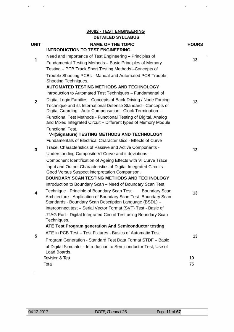
34082 - TEST ENGINEERING
DETAILED SYLLABUS
UNIT NAME OF THE TOPIC HOURS
INTRODUCTION TO TEST ENGINEERING.
1 Need and Importance of Test Engineering – Principles of
13
Fundamental Testing Methods – Basic Principles of Memory
Testing – PCB Track Short Testing Methods –Concepts of
Trouble Shooting PCBs - Manual and Automated PCB Trouble
Shooting Techniques.
AUTOMATED TESTING METHODS AND TECHNOLOGY
Introduction to Automated Test Techniques – Fundamental of
2 Digital Logic Families - Concepts of Back-Driving / Node Forcing 13
Technique and its International Defense Standard - Concepts of
Digital Guarding - Auto Compensation - Clock Termination –
Functional Test Methods - Functional Testing of Digital, Analog
and Mixed Integrated Circuit – Different types of Memory Module
Functional Test.
V-I(Signature) TESTING METHODS AND TECHNOLOGY
Fundamentals of Electrical Characteristics - Effects of Curve
3 Trace, Characteristics of Passive and Active Components - 13
Understanding Composite VI-Curve and it deviations –
Component Identification of Ageing Effects with VI Curve Trace,
Input and Output Characteristics of Digital Integrated Circuits -
Good Versus Suspect interpretation Comparison.
BOUNDARY SCAN TESTING METHODS AND TECHNOLOGY
Introduction to Boundary Scan – Need of Boundary Scan Test
4 Technique - Principle of Boundary Scan Test - Boundary Scan 13
Architecture - Application of Boundary Scan Test- Boundary Scan
Standards - Boundary Scan Description Language (BSDL) –
Interconnect test – Serial Vector Format (SVF) Test - Basic of
JTAG Port - Digital Integrated Circuit Test using Boundary Scan
Techniques.
ATE Test Program generation And Semiconductor testing
5 ATE in PCB Test – Test Fixtures - Basics of Automatic Test
13
Program Generation - Standard Test Data Format STDF – Basic
of Digital Simulator - Introduction to Semiconductor Test, Use of
Load Boards.
Revision & Test 10
Total 75 .

04.12.2017 DOTE, Chennai 25 Page 12 of 67
REFERENCE BOOKS:
1. Test Engineering for Electronic Hardware – S R Sabapathi, Qmax Test Equipments P Ltd., 2011.
2. Practical Electronic Fault Finding and Trouble shooting by Robin Pain
Newnes, Reed Educational and professional publishing Ltd., 1996
3. The Fundamentals of Digital Semiconductor Testing, Floyd, Pearson Education India, Sep-2005

04.12.2017 DOTE, Chennai 25 Page 13 of 67
DIRECTORATE OF TECHNICAL EDUCATION
DIPLOMA IN ELECTRONICS AND COMMUNICATION ENGINEERING
III YEAR
M SCHEME
VI SEMESTER
2015-2016 onwards
PCB DESIGN PRACTICAL
CURRICULAM DEVELOPMENT CENTRE

04.12.2017 DOTE, Chennai 25 Page 14 of 67
M-SCHEME ( Implemented from the Academic Year 2015-2016 onwards )
Course Name : Electronics and Communication Engineering Subject Code : 34084 Semester : VI Semester Subject Title : PCB Design Practical TEACHING AND SCHEME OF EXAMINATIONS Number Of Weeks / Semester : 15 Weeks
Subject Instruction Examination PCB
Design Practical
Hours/ Week
Hours/ Semester
Marks Duration INTERNAL
ASSESSMENT BOARD EXAM
TOTAL
4 60 25 75 100 3 Hrs RATIONALE: This Subject is to appreciate the necessity and evolution of the PCB, types and
classes of PCB. Understand steps involved in schematic, layout, fabrication and assembly
process of PCB design. Understand basic concepts of transmission line and crosstalk Design (schematic and layout)PCB for analog circuits, digital circuits and
mixed circuits. Design (schematic and layout) and fabricate PCB for simple circuit.
Course Objective: 1.Understand the need for PCB Design and steps involved in PCB Design and Fabrication Process 2. Familiarize Schematic and layout Design flow using Electronic Design Automation ( EDA ) Tools

04.12.2017 DOTE, Chennai 25 Page 15 of 67
34084 PCB design Practical
List of Experiments Design the Experiments ( Single side PCB ONLY ) using Any EDA tools like TINA, MultiSim , ORcad
1. Design PCB for Full wave rectifier 2. Design PCB for Bridge rectifier 3. Design PCB for CE or CB or CC Amplifier circuits using discrete
components 4. Design PCB for Amplitude Modulator 5. Design PCB for Frequency Modulator 6. Design PCB for Astable Multivibrator using 555 IC 7. Design PCB for half adder using Logic gates 8. Design PCB for full adder using Logic gates 9. Design PCB for 4 bit binary counter using D Flip Flops 10. Design PCB 4 bit shift Register ( PIPO ) using JK Flip Flops 11. Design PCB for Positive Voltage Regulator using 7805 & 7812 IC 12. Design PCB for Analog Multiplier using 741 IC 13. Design PCB for flashing LEDs using 555 IC 14. Design PCB for Fan Regulator 15. Design PCB for Liquid Level Controller
HARDWARE REQUIREMENT: Desktop/ Laptop Computers : 15 Nos Laser Printer : 2 Nos
ALLOCATION OF MARKS
I) CONSTRUCTION & PROCEDURE : 30
II) IMPORT & PREPARATION : 10
III) PCB LAYOUT : 20
IV) OUTPUT : 10
V) VIVA : 05
TOTAL : 75
04.12.2017 DOTE, Chennai 25 Page 16 of 67
34084 – PCB DESIGN PRACTICAL
List of Experiments with model/example circuit diagrams
Note: The following circuits are example circuits only. During examination
different circuits may be given based on the list of experiments. Students will be asked to design the PCB for the circuits supplied.
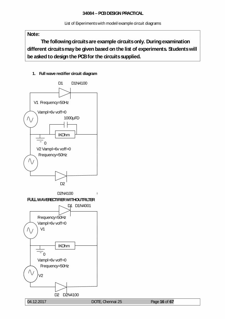
1. Full wave rectifier circuit diagram
D1 D1N4100
V1 Frequency=50Hz
Vampl=6v voff=0 1000µFD
0 V2 Vampl=6v voff=0 Frequency=50Hz
D2
D2N4100 FULL WAVERECTIFIER WITHOUTFILTER D1 D1N4001 Frequency=50Hz Vampl=6v voff=0 V1
0 Vampl=6v voff=0 Frequency=50Hz
V2
D2 D2N4100
IKOhm
IKOhm

04.12.2017 DOTE, Chennai 25 Page 17 of 67
2. Bridge rectifier circuit diagram
D1,D2,D3,D4=1N4100
Frequency=50Hz
Vampl=6v voff=0
3. CE amplifier circuit diagram
15 µfd
c
15 µfd B 2N2714
V2 E
10V 10mvP
VI 100Hz 47µfd
D1 D2
D3
D4
I K Ohm
5.8K
Ohm
1Koh
m
10
Kohm
1K Oh
m
2.2K
ohm

04.12.2017 DOTE, Chennai 25 Page 18 of 67
4. Amplitude Modulator circuit diagram
5. Frequency Modulator

04.12.2017 DOTE, Chennai 25 Page 19 of 67
6. Astable Multibrator using 555 IC circuit diagram
7. Half adder Logic diagram
8. Full adder Logic diagram
SUM =
CARRY =

04.12.2017 DOTE, Chennai 25 Page 20 of 67
9. 4 bit binary counter using D Flip Flop (IC 74LS74)
10. 4 bit shift Register (PIPO) using JK Flip Flop
11. Positive voltage Regulator using 7805 & 7812 IC

04.12.2017 DOTE, Chennai 25 Page 21 of 67
12. Analog Multiplier using 741 IC
13. Flashing LEDs using 555 IC
14. Fan Regulator
04.12.2017 DOTE, Chennai 25 Page 22 of 67
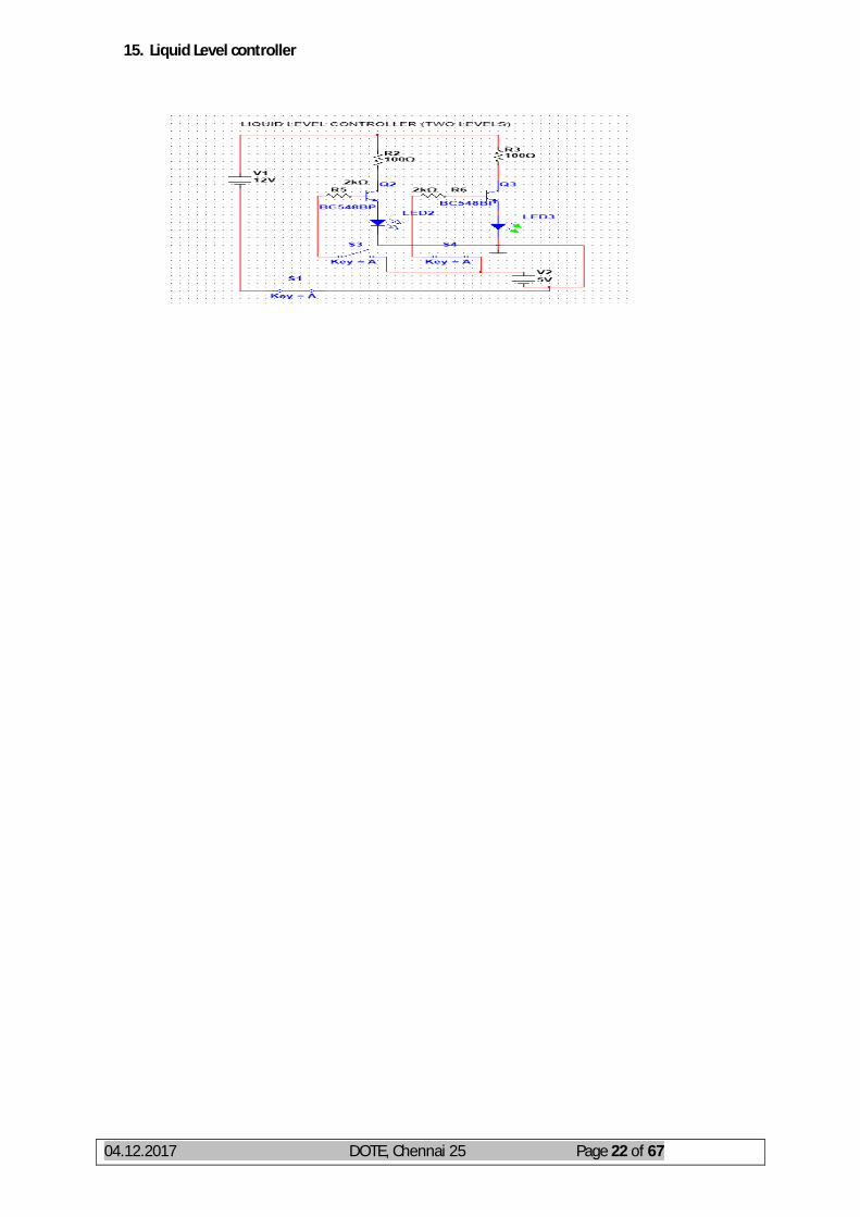
15. Liquid Level controller

04.12.2017 DOTE, Chennai 25 Page 23 of 67
DIRECTORATE OF TECHNICAL EDUCATION
DIPLOMA IN ELECTRONICS AND COMMUNICATION ENGINEERING
III YEAR
M SCHEME
VI SEMESTER
2015-2016 onwards
CURRICULAM DEVELOPMENT CENTRE
TEST ENGINEERING PRACTICAL

04.12.2017 DOTE, Chennai 25 Page 24 of 67
M-SCHEME
(Implemented from the Academic year 2015-2016 onwards)
Course Name: Electronics and Communication Engineering
Subject code : 34085
Semester : VI Semester
Subject title : TEST ENGINEERING PRACTICAL
TEACHING AND SCHEME OF EXAMINATION:
Number of Weeks/ Semester : 15 weeks Subject Instruction Examination
TEST ENGINEERING PRACTICAL
Hrs/ week
Hrs/ semester
Marks Duration INTERNAL
ASSESMENT BOARD EXAM TOTAL
4 60 25 75 100 3Hrs ALLOCATION OF MARKS CIRCUIT DIAGRAM : 20 PROCEDURE: 25 EXECUTION & HANDLING OF EQUIPMENT : 15 OUTPUT / RESULT : 10 VIVA – VOCE: 05 _________________________________________________ TOTAL : 75

04.12.2017 DOTE, Chennai 25 Page 25 of 67
34085 - TEST ENGINEERING PRACTICAL List of experiments
1. Locate a Short in a circuit Board using Short Locator. 2. Test and verify the combinational logic circuits NAND, NOR, Half-Adder, Half-Subtractors, Multiplexers, De-multiplexer, Decoder & Encoder using functional test method. 3. Test and verify the Sequential Logic Circuits D-FF, RS-FF, Latch, Counter, Shift Register using functional test method. 4. Test and verify the Memory Devices SDRAM/DRAM Chip . using functional test method. 5. a. Test and verify the digital circuits in a circuit using auto compensation technique. b.Test and verify the open emitter circuit using pull down resistor. c. .Test and verify the open collector circuit using pull up resistor. 6. Test the functionality of operational amplifier in Inverting , Non-inverting and voltage follower mode. 7. Test the VI characteristics of R,L,C using signature method. 8.Test the VI characteristics of electronic components Diode, Zener Diode, NPN/PNP Transistor using signature method . 9. Test the VI characteristics of RC Filter, Low Pass Filter , Band Pass Filter using signature method. 10. Test the VI characteristics of electronic components MOSFET and Transistor using Trigger pulse and signature method. 11. Test the VI characteristics of electronic components SCR and Opto coupler using Trigger pulse and signature method. 12. Test RLC circuit using in-circuit measurement method. 13..Test the Boundary Scan IC using JTAG port and non boundary scan IC using boundary scan IC. 14.Detect and list down the stuck to VCC and stuck to Gnd pins in a boundary scan IC. 15.Develop a device model for NAND and NOR using device library and create a test pattern for testing.
EQUIPMENTS REQUIRED
Sl.No Name of the Equipments 1 PCB SHORTS LOCATOR TRAINER 2 V-I CHARACTERISTICS TRAINER SYSTEM 3 FUNCTIONAL TESTING TRAINER SYSTEM 4 IN-CIRCUIT MEASUREMENT TRAINER SYSTEM 5 BOUNDARY SCAN TEST TRAINER SYSTEM 6 DIGITAL and ANALOG SIMULATOR

04.12.2017 DOTE, Chennai 25 Page 26 of 67
Annexure II
EMBEDDED SYSTEMS PRACTICAL MANUAL for
VI Semester Diploma in Electronics and Communication
Engineering
Subject Code: 34066
M – Scheme
Prepared by: Convener for ECE Discipline: Dr. M.JEGANMOHAN,M.E.,MBA.,Ph.D.,(Management).,Ph.D.,(Engg).,M.I.S.T.E.,
Principal,
Government Polytechnic College,
Uthappanaickanoor,
Usilampatti, Madurai – 625 537.
Note: This is only a model Manual for Embedded System Practical subjects in VI Semester ECE Department. Since, it is kit Dependent, staff member who is handling the subject can develop programmes according to the kit available in the institutions and taking this model Manual as a reference.
04.12.2017 DOTE, Chennai 25 Page 27 of 67
M-SCHEME
(Implemented from the Academic year 2015-2016 onwards)
Course Name : Electronics and Communication Engineering
Subject code :34066
Semester : VI Semester
Subject title : EMBEDDED SYSTEM PRACTICAL
TEACHING AND SCHEME OF EXAMINATION:
Number of Weeks / Semester : 15 weeks
ALLOCATION OF MARKS
I. Algorithm or Flow chart : 15 Marks
II. Program : 25 Marks
III. Execution : 20 Marks
IV. Result :10 Marks
I. Viva : 5 marks
Total : 75 Marks
Subject Instruction Examination
Embedded system
Practical
Hrs/ week
Hrs/ semest
er
Marks Duration INTERNAL
ASSESMENT BOARD EXAM TOTAL
4 60 25 75 100 3Hrs
04.12.2017 DOTE, Chennai 25 Page 28 of 67
LISTOF EXPERIMENTS
1. STUDY OF ARM PROCESSOR KIT (whatever the ARM processor kit the institution is having) Example: LPC2148 The student should able to Understand the memory mapping of the IO and peripherals List the peripherals present in the processor Explain that how to use an IO pin, related SFRs and instructions Explain that how to use timer, UART, its related SFR and instructions sets
2. SIMULATION OF ARITHMETIC OPERATION ON ARM IN ASSEMBLY Develop an assembly level code for the single precision (32 bit) arithmetic function. a. Addition, b. Subtraction and b. Multiplication (Note: simulate the program in the software)
3. SIMULATION OF ASSEMBLY LEVEL PROGRAM FOR SOFT DELAY Develop an assembly level code for the 32 bit or 64 bit delay routine. Calculate the no of clock taken for the routine and adjust the delay value for the desired. (Note: simulate the program in the software)
4. SIMPLE LED BLINKING WITH VARIABLE SPEED IN ASM Develop an assembly level program of ARM processor to blink a LED (including delay routine) in variable speed in the trainer kit. Upon change in the delay program the speed should vary. No need to change the speed dynamically. (Note: Student should study the list of special function registers associated for accessing the IO pin. Manual containing List of IO registers (SFR for IO) can be given to the students for the final exam)
5. REALIZATION OF INPUT AND OUTPUT PORT IN ASM Develop an assembly level program of ARM processor to read a port in which switches are connected in the trainer kit. Send back the receive input to output in which LEDs are connected in the trainer kit Note: Student should study the list of special function registers associated for accessing Port the read and write. Manual containing List of IO registers (SFR for IO) can be given to the students for the board exam)
6. SIMPLE LED BLINKING WITH VARIABLE SPEED IN C Develop a C program for ARM processor to blink a LED (including delay routine) in variable speed. Upon change in the input switch the speed should vary. (Note: The C code should be in while loop)
7. SEVEN SEGMENT LED DISPLAY INTERFACE IN C Develop a C program for ARM processor to interface a seven segment LED display. The display should count up for every one second.
8. SEVEN SEGMENT LED DISPLAY INTERFACE IN C Develop a C program for ARM processor to interface a seven segment LED display. The display should count up for every one second. The delay can be used from experiment
9. REALIZING TIMER PERIPHERAL IN ARM BY POLLING METHOD Develop a C program for ARM processor to run a timer peripheral in ARM. The timer flag can be pooled for timer end. As timer ends reset the timer and update new value to the LED display.
10. REALIZING TIMER PERIPHERAL IN ARM BY INTERRUPT DRIVEN METHOD Develop a C program for ARM processor to run a timer peripheral in ARM. The timer flag can be pooled for timer end. As timer ends reset the timer and update new value to the LED display.
11. SERIAL TRANSMISSION AND RECEPTION OF A CHARACTER IN C BY POLLING METHOD Write a C Programs for receiving a character from other device (Computer) and send the next character of the received one to the device back. Note: Student should understand the SFRs used for serial

04.12.2017 DOTE, Chennai 25 Page 29 of 67
communication. Manual containing list of SFRs for the UART can be given to the students for their final examination
12. SERIAL TRANSMISSION AND RECEPTION OF A CHARACTER IN C BY INTERRUPT METHOD Write a C Programs for receiving a character from other device (Computer) and send the next character of the received one to the device back.
13. DISPLAYING ALPHANUMERIC CHARACTERS IN 2X16 LINE LCD MODULE Write a C Programs for displaying a number and an alphabet in the LCD module by just calling the built in LCD function. The display should come in the desired line and column. (Built in function for the LCD can be given in the manual)
14. CONVERTING HEXADECIMAL TO DECIMAL AND TO DISPLAY IN LCD Write a C Programs for converting the given 8 bit hexadecimal into decimal and there by converting into ASCII which is to be displayed in the LCD module. (Built in function for the LCD can be given in the manual)
15. ACCESSING INTERNAL ADC OF THE ARM PROCESSOR AND TO DISPLAY IN LCD Write a C Program for reading an ADC, convert into decimal and to display it The ADC input is connected to any analog sensor. (Note: Student should study the SFR associated with ADC, Manual containing List of SFR for accessing ADC can be given for the examination.)
LIST OF EQUIPMENTS AND REQUIREMENTS:
1. ARM7 TDMI Kit – 10 nos with interface boards for the above experiments The Chip set may be TMS470, LPC2138, LPC2148, or STR7 etc
2. Interfaces:RTC, ADC, LCD, Seven segment display, LEDS and Switches.
3. Manual for the kit and for interfacing board with stepper motor
4. Manual for the built in function for the Board.
NOTE:
1. Manual for the ARM instructions sets and manual for the trainer kit (Excluding sample program) can be allowed for their board exam.
2. Definition for built in function for the board can be given to students for their board exam.
3. Manual containing procedure for program down loading through boot loader or JTAG can be given to students for their board exam

04.12.2017 DOTE, Chennai 25 Page 30 of 67
LIST OF EXPERIMENTS:
Ex. No. LAB EXPERIMENT Page No.
1. STUDY OF ARM PROCESSOR KIT - LPC2148 3
2. SIMULATION OF ARITHMETIC OPERATION ON ARM IN ASSEMBLY 5
3. SIMULATION OF ASSEMBLY LEVEL PROGRAM FOR SOFT DELAY 6
4. SIMPLE LED BLINKING WITH VARIABLE SPEED IN ASM 8
5. REALIZATION OF INPUT AND OUTPUT PORT IN ASM 10
6. SIMPLE LED BLINKING WITH VARIABLE SPEED IN C 12
7. SEVEN SEGMENT LED DISPLAY INTERFACE IN C 15
8. SEVEN SEGMENT LED DISPLAY INTERFACE IN C 18
9. REALIZING TIMER PERIPHERAL IN ARM BY POLLING METHOD 20
10. REALIZING TIMER PERIPHERAL IN ARM BY INTERRUPT DRIVEN METHOD 22
11. SERIAL TRANSMISSION AND RECEPTION OF A CHARACTER IN C 24
BY POLLING METHOD
12. SERIAL TRANSMISSION AND RECEPTION OF A CHARACTER IN C 26
BY INTERRUPT METHOD
13. DISPLAYING ALPHANUMERIC CHARACTERS IN 2X16 LINE LCD MODULE 29
14. CONVERTING HEXADECIMAL TO DECIMAL AND TO DISPLAY IN LCD 32
15. ACCESSING INTERNAL ADC OF THE ARM PROCESSOR AND TO DISPLAY IN LCD 35

04.12.2017 DOTE, Chennai 25 Page 31 of 67
Ex.No : 1
STUDY OF ARM PROCESSOR KIT - LPC2148 Date:
Aim To understand the memory mapping of the IO and peripherals, list the peripherals present in the processor, use an IO pin, related SFRs and instructions and use timer, UART, its related SFR and instructions sets Apparatus required
S.No Name of the apparatus Range Quantity
1 LPC2148 ARM Kit 1 IO and UART Memory Map

04.12.2017 DOTE, Chennai 25 Page 32 of 67
#include <NXP/iolpc2148.h> NAME main PUBLIC __iar_program_start SECTION .intvec : CODE (2) CODE32 __iar_program_start B main SECTION .text : CODE (2) CODE32 main NOP LDR R0,=0X5 // Operend-1 stored in R0 . LDR R1,=0XA // Operend-2 stored in R1 . ADD R8,R1,R0 // Addition result is stored in register R8. // Logic : R8 = R0 + R1 SUB R9,R1,R0 // Subtraction result is stored in register R9. // Logic : R9 = R1 + R0 MUL R10, R1,R0 /* For less than 32-bit result.*/ // Logic : R9 = R1 * R0 /* R0 : 32-bit Operend-1 & /* R1 : 32-bit Operend-2 /* R1*R0 : 32-bit (maximum) Output result.*/ /* Result is stored in 32-bit register. ( R10 )*/ UMULL R11,R12,R1,R0 /* For more than 32-bit result.*/ /* R0 : 32-bit Operend-1 & /* R1 : 32-bit Operend-2 /* R1*R0 : 64-bit (maximum) Output result.*/ /* To store the multiplication result 64-bits are needed. Here, Two 32-bit registers are used to store the multiplication result. R11 : It stores the LSB of the multiplication result. & R12 : It stores the MSB of the multiplication result.*/ stop B stop // Halt the program. END

04.12.2017 DOTE, Chennai 25 Page 33 of 67
Ex.No : 2
SIMULATION OF ARITHMETIC OPERATION ON ARM IN ASSEMBLY Date:
Aim To develop an assembly level code for the single precision (32 bit) arithmetic functions following a. Addition, b. Subtraction and C. Multiplication Apparatus required
S.No Name of the apparatus Range Quantity
1 Personal Computer setup P4 (XP loaded) 1
2 LPC2148 ARM Kit 1
3 Software used IAR & Flash Magic 1 #include <nxp\iolpc2148.h> NAME This_is_an_Assembly_Code. // Any name PUBLIC __iar_program_start SECTION .intvec : CODE (2) CODE32 __iar_program_start B main SECTION .text : CODE (2) CODE32 delay LDR R0,=1000 // 32-bit delay1 value Loop1: LDR R1,=400 // 32-bit delay2 value Loop2: SUBS R1,R1,#1 /* So total Delay = 32+32 = 46 bit delay routine */ BNE Loop2 SUBS R0,R0,#1 BNE Loop1 MOV PC,LR // return statement main NOP //To Select the p1.16-p1.23 as gpio lines BL delay END

04.12.2017 DOTE, Chennai 25 Page 34 of 67
Ex.No : 3
SIMULATION OF ASSEMBLY LEVEL PROGRAM FOR SOFT DELAY Date:
Aim To develop an assembly level code for the 32 bit or 64 bit delay routine. Calculate the no of clock taken for the routine and adjust the delay value for the desired. Apparatus required
S.No Name of the apparatus Range Quantity
1 Personal Computer setup P4 (XP loaded) 1
2 LPC2148 ARM Kit 1
3 Software used IAR & Flash Magic 1
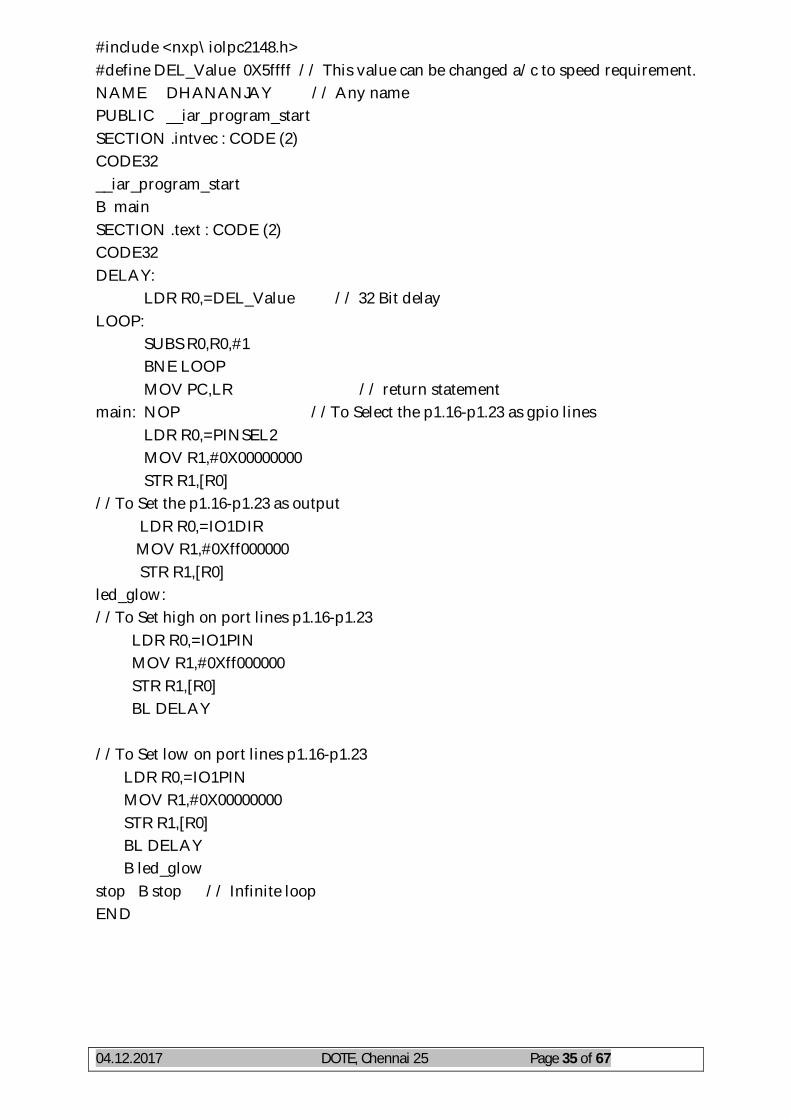
04.12.2017 DOTE, Chennai 25 Page 35 of 67
#include <nxp\iolpc2148.h> #define DEL_Value 0X5ffff // This value can be changed a/c to speed requirement. NAME DHANANJAY // Any name PUBLIC __iar_program_start SECTION .intvec : CODE (2) CODE32 __iar_program_start B main SECTION .text : CODE (2) CODE32 DELAY: LDR R0,=DEL_Value // 32 Bit delay LOOP: SUBS R0,R0,#1 BNE LOOP MOV PC,LR // return statement main: NOP //To Select the p1.16-p1.23 as gpio lines LDR R0,=PINSEL2 MOV R1,#0X00000000 STR R1,[R0] //To Set the p1.16-p1.23 as output LDR R0,=IO1DIR MOV R1,#0Xff000000 STR R1,[R0] led_glow: //To Set high on port lines p1.16-p1.23 LDR R0,=IO1PIN MOV R1,#0Xff000000 STR R1,[R0] BL DELAY //To Set low on port lines p1.16-p1.23 LDR R0,=IO1PIN MOV R1,#0X00000000 STR R1,[R0] BL DELAY B led_glow stop B stop // Infinite loop END

04.12.2017 DOTE, Chennai 25 Page 36 of 67
Ex.No : 4
SIMPLE LED BLINKING WITH VARIABLE SPEED IN ASM Date:
Aim To develop an assembly level program of ARM processor to blink a LED (including delay routine) in variable speed in the trainer kit. Change in the delay program the different speed variation without changing the speed dynamically. (Set IO pin in SFR) Apparatus required
S.No Name of the apparatus Range Quantity
1 Personal Computer setup P4 (XP loaded) 1
2 LPC2148 ARM Kit 1
3 Software used IAR & Flash Magic 1
Pin Detail
LED0 – LED7: P1.24 – P1.31

04.12.2017 DOTE, Chennai 25 Page 37 of 67
#include <nxp\iolpc2148.h> NAME LED_SWITCH // Any name PUBLIC __iar_program_start SECTION .intvec : CODE (2) CODE32 __iar_program_start B main SECTION .text : CODE (2) CODE32 delay: LDR R0,=0Xf // delay value LOOP: SUBS R0,R0,#1
BNE LOOP MOV PC,LR // return statement
main: NOP LDR R0,=PINSEL1 MOV R1,#0X00000000 // Configure the port as GPIO. STR R1,[R0] LDR R0,=PINSEL2 MOV R1,#0X00000000 // Configure the port as GPIO . STR R1,[R0] LDR R0,=IO1DIR MOV R1,#0Xff000000 //To Set the p0.24-p0.31 as output ( LED ) STR R1,[R0] LDR R0,=IO0DIR MOV R1,#0X00000000 //To Set the p0.16-p1.23 as input ( SWITCH ) STR R1,[R0] GLOW_LED : LDR R0,=IO0PIN // READ the SWITCHs address in R0 LDR R1,[R0] // Move the read value from R0 to R1 LSL R1,R1,#8 // Shift the value 8-bit left MOV R2,#0XFF000000 AND R2,R2,R1 // Make unused bits = 0 LDR R0,=IO1PIN // STORE LEDs address to R0 STR R2,[R0] // Store the switches value at LED address BL delay // After some delay B GLOW_LED // Repeat the same forever stop B stop // Halt END

04.12.2017 DOTE, Chennai 25 Page 38 of 67
Ex.No : 5
REALIZATION OF INPUT AND OUTPUT PORT IN ASM Date:
Aim To develop an assembly level program of ARM processor to read a port in which switches are connected in the trainer kit. Send back the receive input to output in which LEDs are connected in the trainer kit (Access I/O PORT for Read and Write) Apparatus required
S.No Name of the apparatus Range Quantity
1 Personal Computer setup P4 (XP loaded) 1
2 LPC2148 ARM Kit 1
3 Software used IAR & Flash Magic 1 Pin Details SW0 - SW7: P0.16 - P0.23 LED0 - LED7: P1.23 - P1.31

04.12.2017 DOTE, Chennai 25 Page 39 of 67
#include<lpc21xx.h>
int main(void)
{
int i;
while(1)
{
*IODIR0 = *IODIR0 |0X007f8000;
*IOSET0 = 0X1A8000;
for(i=0;i<=200000;i++);
*IOCLR0=0X1A8000;
*IOSET0 = 0X550000;
for(i=0;i<=200000;i++);
}
return 0;
}
04.12.2017 DOTE, Chennai 25 Page 40 of 67
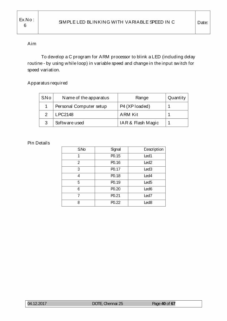
Ex.No : 6
SIMPLE LED BLINKING WITH VARIABLE SPEED IN C Date:
Aim To develop a C program for ARM processor to blink a LED (including delay routine - by using while loop) in variable speed and change in the input switch for speed variation. Apparatus required
S.No Name of the apparatus Range Quantity
1 Personal Computer setup P4 (XP loaded) 1
2 LPC2148 ARM Kit 1
3 Software used IAR & Flash Magic 1 Pin Details
S.No Signal Description 1 P0.15 Led1 2 P0.16 Led2
3 P0.17 Led3 4 P0.18 Led4 5 P0.19 Led5 6 P0.20 Led6
7 P0.21 Led7
8 P0.22 Led8
04.12.2017 DOTE, Chennai 25 Page 41 of 67
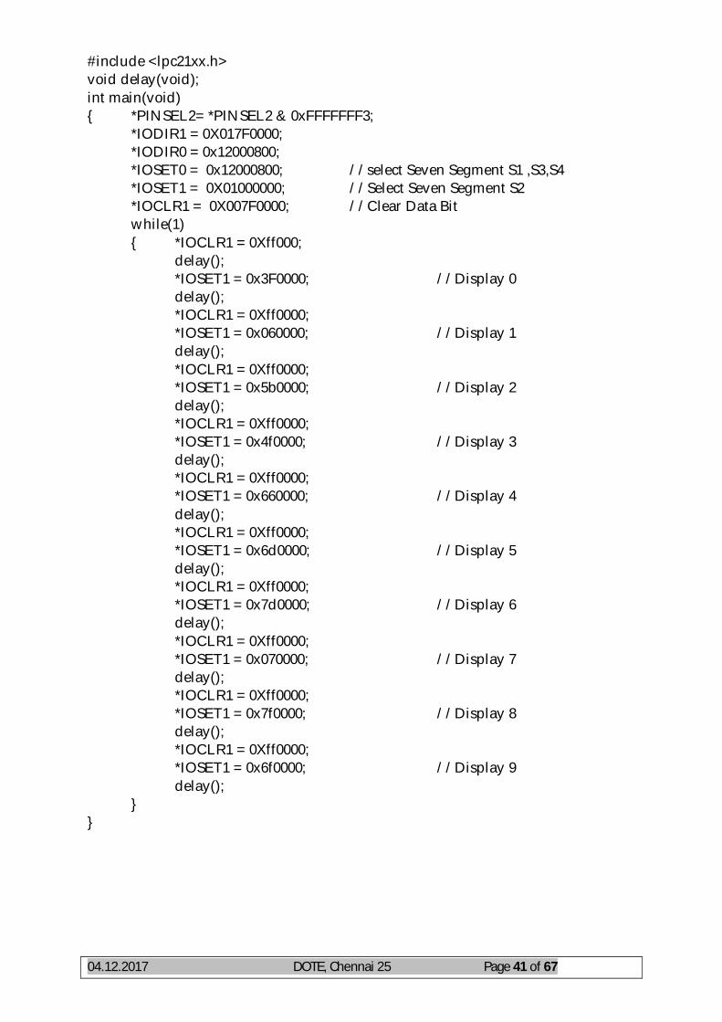
#include <lpc21xx.h> void delay(void); int main(void) { *PINSEL2= *PINSEL2 & 0xFFFFFFF3; *IODIR1 = 0X017F0000; *IODIR0 = 0x12000800; *IOSET0 = 0x12000800; //select Seven Segment S1 ,S3,S4 *IOSET1 = 0X01000000; //Select Seven Segment S2 *IOCLR1 = 0X007F0000; //Clear Data Bit while(1) { *IOCLR1 = 0Xff000; delay();
*IOSET1 = 0x3F0000; //Display 0 delay(); *IOCLR1 = 0Xff0000;
*IOSET1 = 0x060000; //Display 1 delay(); *IOCLR1 = 0Xff0000;
*IOSET1 = 0x5b0000; //Display 2 delay(); *IOCLR1 = 0Xff0000;
*IOSET1 = 0x4f0000; //Display 3 delay(); *IOCLR1 = 0Xff0000;
*IOSET1 = 0x660000; //Display 4 delay(); *IOCLR1 = 0Xff0000;
*IOSET1 = 0x6d0000; //Display 5 delay(); *IOCLR1 = 0Xff0000;
*IOSET1 = 0x7d0000; //Display 6 delay(); *IOCLR1 = 0Xff0000;
*IOSET1 = 0x070000; //Display 7 delay(); *IOCLR1 = 0Xff0000;
*IOSET1 = 0x7f0000; //Display 8 delay(); *IOCLR1 = 0Xff0000;
*IOSET1 = 0x6f0000; //Display 9 delay(); } }

04.12.2017 DOTE, Chennai 25 Page 42 of 67
void delay(void) { int j; for (j=0;j<100000;j++); for (j=0;j<100000;j++); for (j=0;j<100000;j++); for (j=0;j<100000;j++); for (j=0;j<100000;j++); }

04.12.2017 DOTE, Chennai 25 Page 43 of 67
Ex.No : 7
SEVEN SEGMENT LED DISPLAY INTERFACE IN C Date:
Aim To develop a C program for ARM processor to interface a seven segment LED display and count up for every one second Apparatus required
S.No Name of the apparatus Range Quantity
1 Personal Computer setup P4 (XP loaded) 1
2 LPC2148 ARM Kit 1
3 Software used IAR & Flash Magic 1 Pin Details
S.No Signal description 1 P1.16 ‘a’ 2 P1.17 ‘b’ 3 P1.18 ‘c’ 4 P1.19 ‘d’ 5 P1.20 ‘e’ 6 P1.21 ‘f’ 7 P1.22 ‘g’ 8 P1.23 ‘.’

04.12.2017 DOTE, Chennai 25 Page 44 of 67
#include <lpc21xx.h> void delay(void); int main(void) { *PINSEL2= *PINSEL2 & 0xFFFFFFF3; *IODIR1 = 0X017F0000; *IODIR0 = 0x12000800; *IOSET0 = 0x12000800; //select Seven Segment S1 ,S3,S4 *IOSET1 = 0X01000000; //Select Seven Segment S2 *IOCLR1 = 0X007F0000; //Clear Data Bit while(1) { *IOCLR1 = 0Xff000; delay();
*IOSET1 = 0x3F0000; //Display 0 delay(); *IOCLR1 = 0Xff0000;
*IOSET1 = 0x060000; //Display 1 delay(); *IOCLR1 = 0Xff0000;
*IOSET1 = 0x5b0000; //Display 2 delay(); *IOCLR1 = 0Xff0000;
*IOSET1 = 0x4f0000; //Display 3 delay(); *IOCLR1 = 0Xff0000;
*IOSET1 = 0x660000; //Display 4 delay(); *IOCLR1 = 0Xff0000;
*IOSET1 = 0x6d0000; //Display 5 delay(); *IOCLR1 = 0Xff0000;
*IOSET1 = 0x7d0000; //Display 6 delay(); *IOCLR1 = 0Xff0000;
*IOSET1 = 0x070000; //Display 7 delay(); *IOCLR1 = 0Xff0000;
*IOSET1 = 0x7f0000; //Display 8 delay(); *IOCLR1 = 0Xff0000;
*IOSET1 = 0x6f0000; //Display 9 delay(); } }

04.12.2017 DOTE, Chennai 25 Page 45 of 67
void delay(void) { int j; for (j=0;j<100000;j++); for (j=0;j<100000;j++); for (j=0;j<100000;j++); for (j=0;j<100000;j++); for (j=0;j<100000;j++); }

04.12.2017 DOTE, Chennai 25 Page 46 of 67
Ex.No : 8
SEVEN SEGMENT LED DISPLAY INTERFACE IN C Date:
Aim To develop a C program for ARM processor to interface a seven segment LED display by using delay routine and count up for every one second. (The delay can be used from experiment 3) Apparatus required
S.No Name of the apparatus Range Quantity
1 Personal Computer setup P4 (XP loaded) 1
2 LPC2148 ARM Kit 1
3 Software used IAR & Flash Magic 1 Pin Details
S.No Signal Description 1 P1.16 ‘a’ 2 P1.17 ‘b’ 3 P1.18 ‘c’ 4 P1.19 ‘d’ 5 P1.20 ‘e’ 6 P1.21 ‘f’ 7 P1.22 ‘g’ 8 P1.23 ‘.’

04.12.2017 DOTE, Chennai 25 Page 47 of 67
#include<lpc21xx.h> #include<board.h> void TIMER_ISR (void) __attribute__ ((interrupt ("IRQ"))); #define TIMER 4; int main(void) { *T0MCR=0x03; *T0MR0=0xf59100; *T0TCR=0x01; *VICIntEnable=0x10; *VICVectCntl0=0x20 |TIMER; *VICVectAddr0=(unsigned int)TIMER_ISR; return 0; } void TIMER_ISR() { *IODIR0=0x007F8000; static int flag=1; if(flag) { *IOCLR0=0x007F8000; flag=0; } else { *IOSET0=0x007F8000; flag=1; } *VICVectAddr=0X00; *T0IR=0X01; }

04.12.2017 DOTE, Chennai 25 Page 48 of 67
Ex.No : 9
REALIZING TIMER PERIPHERAL IN ARM BY POLLING METHOD Date:
Aim To develop a C program for ARM processor to run a timer peripheral in ARM. The timer flag can be pooled for timer end. As timer ends reset the timer and update new value to the LED display. Apparatus required
S.No Name of the apparatus Range Quantity
1 Personal Computer setup P4 (XP loaded) 1
2 LPC2148 ARM Kit 1
3 Software used IAR & Flash Magic 1

04.12.2017 DOTE, Chennai 25 Page 49 of 67
#include<lpc21xx.h> #include<board.h> void TIMER_ISR (void) __attribute__ ((interrupt ("IRQ"))); #define TIMER 4; int main(void) { *T0MCR=0x03; *T0MR0=0xf59100; *T0TCR=0x01; *VICIntEnable=0x10; *VICVectCntl0=0x20 |TIMER; *VICVectAddr0=(unsigned int)TIMER_ISR; return 0; } void TIMER_ISR() { *IODIR0=0x007F8000; static int flag=1; if(flag) { *IOCLR0=0x007F8000; flag=0; } else { *IOSET0=0x007F8000; flag=1; } *VICVectAddr=0X00; *T0IR=0X01; }

04.12.2017 DOTE, Chennai 25 Page 50 of 67
Ex.No : 10
REALIZING TIMER PERIPHERAL IN ARM BY INTERRUPT DRIVEN METHOD Date:
Aim To develop a C program for ARM processor to run a timer peripheral in ARM. The timer flag can be pooled for timer end. As timer ends reset the timer and update new value to the LED display. Apparatus required
S.No Name of the apparatus Range Quantity
1 Personal Computer setup P4 (XP loaded) 1
2 LPC2148 ARM Kit 1
3 Software used IAR & Flash Magic 1
04.12.2017 DOTE, Chennai 25 Page 51 of 67
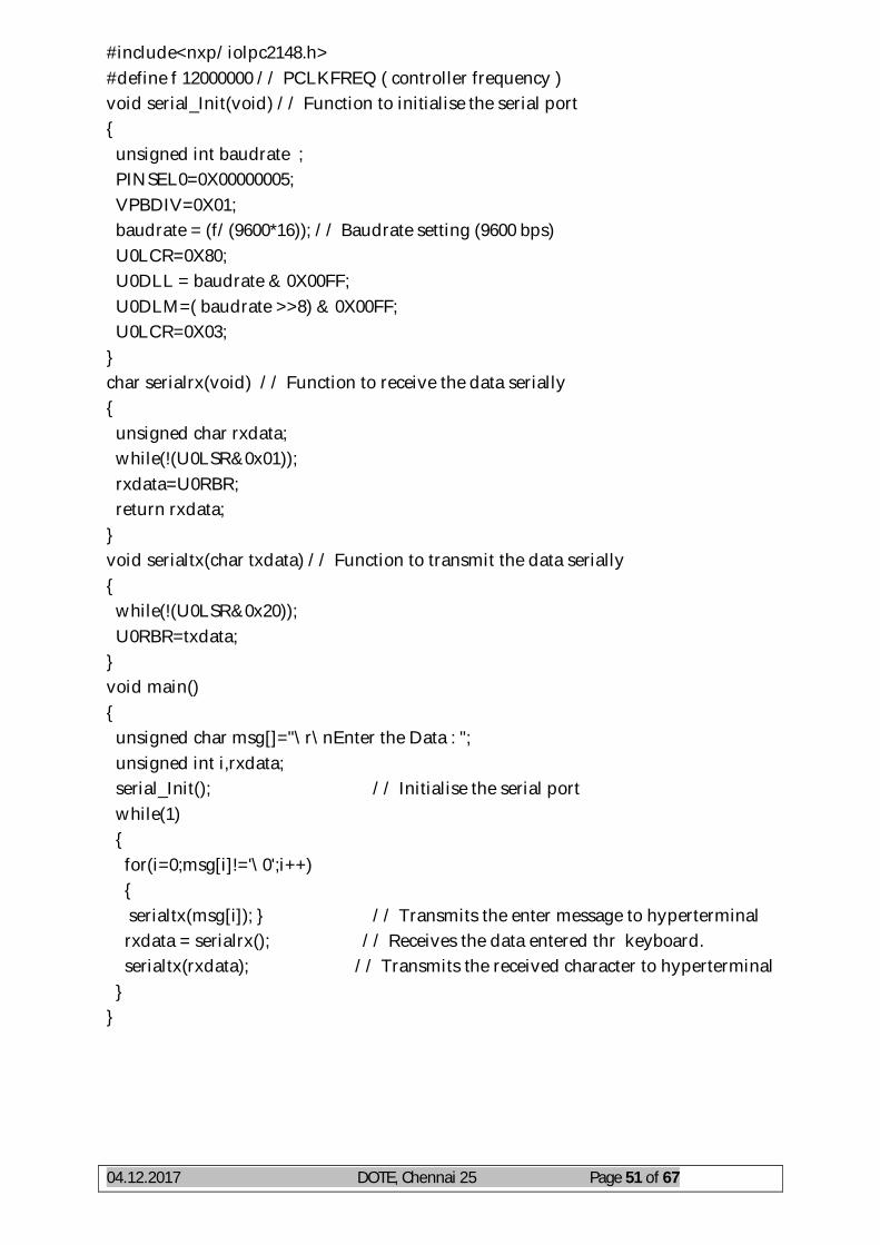
#include<nxp/iolpc2148.h> #define f 12000000 // PCLKFREQ ( controller frequency ) void serial_Init(void) // Function to initialise the serial port { unsigned int baudrate ; PINSEL0=0X00000005; VPBDIV=0X01; baudrate = (f/(9600*16)); // Baudrate setting (9600 bps) U0LCR=0X80; U0DLL = baudrate & 0X00FF; U0DLM=( baudrate >>8) & 0X00FF; U0LCR=0X03; } char serialrx(void) // Function to receive the data serially { unsigned char rxdata; while(!(U0LSR&0x01)); rxdata=U0RBR; return rxdata; } void serialtx(char txdata) // Function to transmit the data serially { while(!(U0LSR&0x20)); U0RBR=txdata; } void main() { unsigned char msg[]="\r\nEnter the Data : "; unsigned int i,rxdata; serial_Init(); // Initialise the serial port while(1) { for(i=0;msg[i]!='\0';i++) { serialtx(msg[i]); } // Transmits the enter message to hyperterminal rxdata = serialrx(); // Receives the data entered thr keyboard. serialtx(rxdata); // Transmits the received character to hyperterminal } }

04.12.2017 DOTE, Chennai 25 Page 52 of 67
Ex.No : 11
SERIAL TRANSMISSION AND RECEPTION OF A CHARACTER IN C BY POLLING METHOD Date:
Aim To Write a C Programs for receiving a character from other device (Computer) and send the next character of the received one to the device back. (Set SFR for the UART) Apparatus required
S.No Name of the apparatus Range Quantity
1 Personal Computer setup P4 (XP loaded) 1
2 LPC2148 ARM Kit 1
3 Software used IAR & Flash Magic 1

04.12.2017 DOTE, Chennai 25 Page 53 of 67
#include <nxp/iolpc2148.h> #include <intrinsics.h> // Header Files #include <stdio.h> void UART0_ISR(); // UART-0 ISRdeclaation void UART0_init(); // UART-0 Initialisation function declaration void feed (void); // PLL-FEED function declaration void serialtx(char txdata); // UART-0 Serial Transmitter declaration __irq __arm void irq_handler (void); // IRQ Handler function declaration __fiq __arm void fiq_handler (void); // FIQ Handler Service Routine function void main(void) { unsigned char msg[]="\r\n UART0 Interrupt Program. "; PINSEL2 = 0X00000000; IO1DIR = 0xff000000; // data bits configuration as I/O UART0_init(); // UART0 Initialisation Function __enable_interrupt(); // Global interrupt enable for(int i=0;msg[i]!='\0';i++) { serialtx(msg[i]); } // Transmits the enter message to hyperterminal while(1) {
IO1PIN = 0x55000000; } } void UART0_ISR() // ISR for TIMER0 interrupt. { int temp,buf; __disable_interrupt(); // Global interrupt disable. IO1PIN = 0xAA000000; // LED glow in this pattern (0xAA)when there is an interrupt. for(int i = 0; i < 10000; ++i) // few ms Delay temp = U0IIR; // Checking the Interrupt Identification Register temp =( temp>>1 )& 0x07; // Filtering the useful bits. if (temp==2) // If interrupt is invoked {while (U0LSR & 0x01) {
buf=U0RBR; // Receiving the data from RxD pin serialtx(buf); // Sending the data to TxD pin. } } __enable_interrupt(); // Global interrupt enable VICVectAddr = 0; // Clear interrupt in VIC to return in the main }

04.12.2017 DOTE, Chennai 25 Page 54 of 67
Ex.No : 12
SERIAL TRANSMISSION AND RECEPTION OF A CHARACTER IN C BY INTERRUPT METHOD Date:
Aim To Write a C Programs for receiving a character from other device (Computer) and send the next character of the received one to the device back Apparatus required
S.No Name of the apparatus Range Quantity
1 Personal Computer setup P4 (XP loaded) 1
2 LPC2148 ARM Kit 1
3 Software used IAR & Flash Magic 1

04.12.2017 DOTE, Chennai 25 Page 55 of 67
void UART0_init() // UART0 and Interrupt initialisation for TIMER0 interrupt. { PLLCON_bit.PLLC = PLLCON_bit.PLLE = 0; // Disable and disconnect PLL feed(); // PLL feed sequence VPBDIV_bit.VPBDIV = 0; /* Init Peripherial divider Pckl = Clk/4 */ /*------- UART0 Setting -------------*/ PINSEL0=0X00000005; // Selecting/configuring the pins as RxD & TxD. VPBDIV=0X01; // Making Pclk = Xclk. int baudrate = (12000000/(9600*16)); // Baudrate setting (9600 bps) U0LCR=0X80; U0DLL = baudrate & 0X00FF; U0DLM=( baudrate >>8) & 0X00FF; U0LCR=0X03; U0IER = 0x01; //* Enable UART0 interrupt /*------- Vector Interrupt Setting -------------*/ VICIntSelect = 0; // Set all VIC interrupts to IRQ for now VICIntEnClear = 0xFFFFFFFF; // Diasable all interrupts VICProtection = 0; // VIC registers can be accessed in User or privileged mode VICVectAddr = 0; // Clear interrupt VICProtection = 0; // Accesss VIC in USR | PROTECT VICIntSelect &= ~(1<<VIC_UART0); // Timer 0 intrpt is an IRQ (VIC_TIMER0 = 4) VICVectAddr0 = (unsigned int)&UART0_ISR; // Install ISR in VIC addr slot 0 VICVectCntl0 = 0x20 | VIC_UART0; // IRQ type, TIMER 0 int enabled VICIntEnable |= (1<<VIC_UART0); // Turn on Timer0 Interrupt } __irq __arm void irq_handler (void) /*------ IRQ Handler Function ---------*/ { void (*interrupt_function)(); // Get interrupt vector. interrupt_function = (void(*)())VICVectAddr; // Call UART0_ISR thru pointer (*interrupt_function)(); // Call vectored interrupt function VICVectAddr = 0; // Clear interrupt in VIC to return the pointer to main function. } __fiq __arm void fiq_handler (void) /*------ FIQ Handler Function ---------*/ { while(1);} void feed (void) // PLL FEED Function. { PLLFEED=0xAA; PLLFEED=0x55; } void serialtx(char txdata) // Function to transmit the data serially { while(!(U0LSR&0x20)); // Checking the Line Status Register ( i.e. Tx flag ) U0RBR=txdata; // Transmitting the data byte. }

04.12.2017 DOTE, Chennai 25 Page 56 of 67
#include<nxp\iolpc2148.h> #define EN 0x800 // P0.11 for "LCD_ENABLE" #define RW 0X200 // P0.9 for "Read/Write" #define RS 0x100 // P0.8 for "Register Select" void delay(void) { unsigned int i; for(i=0;i<0x1fff;i++); } void EN_Pulse(void) { IO0SET = EN ; // Enable pin High delay( ); IO0CLR = EN ; // Enable pin Low } void send_cmd( int addr ) // Function to send commands to the LCD reg. { IO1PIN = addr<<16; IO0CLR = RS; EN_Pulse(); } void send_data( int data ) // Function to send data to the LCD reg. { IO1PIN = data<<16; IO0SET = RS; EN_Pulse(); } void lcd_initialize(void) /*------- LCD initialisation function -----*/ { send_cmd( 0X38 ); delay( ); /* INIT. LCD 2 LINES, 5X7 MATRIX */ send_cmd( 0X0F ); delay( ); /* Display on, cursor on */ send_cmd( 0X01 ); delay( ); /* Clear LCD */ send_cmd( 0X06 ); delay( ); /* Shift cursor right */ send_cmd( 0X80 ); delay( ); /* Cursor at line 1, pos. 0 */ }

04.12.2017 DOTE, Chennai 25 Page 57 of 67
Ex.No : 13
DISPLAYING ALPHANUMERIC CHARACTERS IN 2X16 LINE LCD MODULE Date:
Aim To Write a C Programs for displaying a number and an alphabet in the LCD module by just calling the built in LCD function and set the display in the desired line and column. Apparatus required
S.No Name of the apparatus Range Quantity
1 Personal Computer setup P4 (XP loaded) 1
2 LPC2148 ARM Kit 1
3 Software used IAR & Flash Magic 1 Pin Details //LCD0-LCD7 - P1.16 to P1.23 //RS - P0.8 //DIOW - P0.9 //LCDEN - P0.11

04.12.2017 DOTE, Chennai 25 Page 58 of 67
void main(void) { unsigned char alphabets[16]= {"Vi Microsystems "}; // Alphabets array unsigned char numbers[16] = {" 0123456789 "}; // Numbers array unsigned char i=0,j=0,line1=0x8, line2=0xC0; PINSEL0 = 0X00000000; PINSEL1 = 0x00000000; // PINSEL(0,1,2) = 0 configures the pins as GPIO PINSEL2 = 0X00000000; // ( Optional ) IO0DIR = 0x00000f00; // command bits configuration as I/O IO1DIR = 0x00ff0000; // data bits configuration as I/O IO0CLR = RW; // LCD in Write mode lcd_initialize(); // Initialise the LCD for(j=0;j<1;j++) { for(i=0;i<16;i++) // writing Alphabets in upper line { send_cmd ( line1+i ); delay( ); send_data( alphabets[i]); delay( ); } for(i=0;i<16;i++) // writing Numbers in lower line { send_cmd ( line2+i ); delay( ); send_data( numbers[i]); delay( ); } } }

04.12.2017 DOTE, Chennai 25 Page 59 of 67
#include "lpc214x.h" #define EN 0x800 #define RW 0X200 #define RS 0x100 void delay(void) { unsigned int i; for(i=0;i<0x1fff;i++); } void EN_Pulse(void) { IO0SET = EN; delay(); IO0CLR = EN; } void send_cmd(int addr) { IO1PIN = addr<<16; IO0CLR = RS; EN_Pulse(); } void send_data(int data) { IO1PIN = data<<16; IO0SET = RS; EN_Pulse(); } void lcd_initialize(void) { send_cmd(0X38); delay(); send_cmd(0X0F); delay(); send_cmd(0X01); delay(); send_cmd(0X06); delay(); send_cmd(0X80); delay(); }
04.12.2017 DOTE, Chennai 25 Page 60 of 67
Ex.No : 14
CONVERTING HEXADECIMAL TO DECIMAL AND TO DISPLAY IN LCD Date:
Aim To Write a C Programs for converting the given 8 bit hexadecimal into decimal and there by converting into ASCII which is to be displayed in the LCD module. Apparatus required
S.No Name of the apparatus Range Quantity
1 Personal Computer setup P4 (XP loaded) 1
2 LPC2148 ARM Kit 1
3 Software used IAR & Flash Magic 1

04.12.2017 DOTE, Chennai 25 Page 61 of 67
int main(void) { int num,i,d1,d2,d3; char *display = "Decimal value = "; IO0DIR = 0x00000F00; IO1DIR = 0x00FF0000; IO0CLR = RW; lcd_initialize(); num = 0xFF; d1 = num % 10; num = num / 10; d2 = num % 10; num = num / 10; d3 = num; send_cmd(0x80); delay(); for(i=0;i<=15; i++) { send_data(display[i]); } send_cmd (0xc0); delay(); send_data(d3+48); delay(); send_data(d2+48); delay(); send_data(d1+48); delay(); while(1) { } }

04.12.2017 DOTE, Chennai 25 Page 62 of 67
#include "lpc214x.h" #define EN 0x800 #define RW 0X200 #define RS 0x100 #define DONE 0x80000000 #define START 0x01000000 #define PRESET 0x00230600 void delay(void) { unsigned int i; for(i=0;i<0x1fff;i++); } void EN_Pulse(void) { IO0SET = EN ; delay(); IO0CLR = EN ; } void send_cmd( int addr ) { IO1PIN = addr<<16; IO0CLR = RS; EN_Pulse(); } void send_data( int data ) { IO1PIN = data<<16; IO0SET = RS; EN_Pulse(); } void lcd_initialize(void) {send_cmd(0X38); delay(); send_cmd(0X0F); delay(); send_cmd(0X01); delay(); send_cmd(0X06); delay(); send_cmd(0X80); delay(); }

04.12.2017 DOTE, Chennai 25 Page 63 of 67
Ex.No : 15
ACCESSING INTERNAL ADC OF THE ARM PROCESSOR AND TO DISPLAY IN LCD Date:
Aim To Write a C Programs for reading an ADC input from analog sensor then convert into decimal and display it. (Set SFR for ADC access) Apparatus required
S.No Name of the apparatus Range Quantity
1 Personal Computer setup P4 (XP loaded) 1
2 LPC2148 ARM Kit 1
3 Software used IAR & Flash Magic 1

04.12.2017 DOTE, Chennai 25 Page 64 of 67
int main(void) { int num,i,d1,d2,d3,d4; unsigned long Val; char *display = "Digital value = "; PINSEL1 = 0x01 << 24; IO0DIR = 0x00000F00; IO1DIR = 0x00FF0000; IO0CLR = RW; AD0CR = PRESET | 0x02; AD0CR |= START; lcd_initialize(); send_cmd(0x80); delay(); for(i=0;i<=15; i++) { send_data(display[i]); } while(1) { do { Val = AD0GDR; } while ((Val & DONE) == 0); Val = ((AD0GDR >> 6) & 0x3FF); num = Val; d1 = num % 10; num = num / 10; d2 = num % 10; num = num / 10; d3 = num % 10; num = num / 10; d4 = num; send_cmd (0xc0); delay(); send_data(d4+48); delay(); send_data(d3+48); delay(); send_data(d2+48); delay(); send_data(d1+48); delay(); }}
04.12.2017 DOTE, Chennai 25 Page 65 of 67
Procedure: (using Triton software)
1. Double click triton icon click OK select project option select C++ project New window will open in that give your project name select LPC2148 Click next select executable GNU click next select project that have been already given click next.
2. A new window will open with the project name. In left pan of that project name click + symbol
3. To type a C language program double click project name_main.c the new text window will open Type C language program in that text window and save it.
4. To type assembly language program double click project name_main.s the new text window will open Type assembly language program in that text windows and save it.
5. Right click Project name Select Active Build configuration select release mode
6. Again right click the project name Select build project (to verify program) 7. After execution of the project the HEX file will created under the RELEASE
in left pan of the release click + symbol then we have to download that HEX file in to the KIT
8. Before downloading the HEX file, change the Mode from RUN to ISP in the KIT right click RELEASE right click the project name.hex file select download press reset button in the kit
9. Then change mode from ISP to RUN in the kit press reset button in the kit to display the result in hyper terminal window
10. To see the result in hyper terminal Tools menu select hyper terminal select 38400 (or) verify the result in kit.

04.12.2017 DOTE, Chennai 25 Page 66 of 67
Procedure (Experiment using IAR kit) 1. Click Project Create New Project C Main (for C Program)
/ASM(Assembly Language Program) Enter the Name of the Project.
2. Click the name of the project name and right click options a) General option: Device NXP LPC2148 b) Output converter: √ Generate additional output
Output format : Intel extended Output file : √ Override default
c) Linker Browse for LPC2148_flash.icf, then enter OK
3. Now enter the program in the editor 4. Right click the project name and select build option. If the errors in code it
will show bottom of the editor otherwise it will create HEX file for the program
5. To flash the HEX file, Open the flash magic and browse for HEX file, before that in KIT, the control key is switched to program mode and press reset button
6. To check for output, switch the key of execute mode and press enter

04.12.2017 DOTE, Chennai 25 Page 67 of 67
Block Diagram – LPC2148

![[]l n-n · 2017-09-13 · Number Dote o{ lssue Dote of expiry Ploce of lssue 5. Possporl Detoiis 6. Dote of Birth 7. Notionolity B. Occupotion 9. Telephone 10. Nominee (s) Olfice:](https://img.dokumen.tips/doc/110x75/5e46dbae1cfecd58ee7c2537/l-n-n-2017-09-13-number-dote-o-lssue-dote-of-expiry-ploce-of-lssue-5-possporl.jpg)