Embed Size (px)
Citation preview

Departmentof ComputingScienceandMathematicsUniversityof Stirling
ExtendedDILL: Digital Logic in LOTOS
Ji He and KennethJ. Turner
TechnicalReportCSM-142
November 1997

Ji He and Kenneth J. Turner. Extended DILL: Digital Logic in LOTOS.Technical Report CSM-142, Department of Computing Science and Mathematics,University of Stirling, Scotland, November 1997.

Ji He and Kenneth J. Turner. Extended DILL: Digital Logic in LOTOS.Technical Report CSM-142, Department of Computing Science and Mathematics,University of Stirling, Scotland, November 1997.
Departmentof ComputingScienceandMathematicsUniversityof Stirling
ExtendedDILL: Digital Logic in LOTOS
Ji He and KennethJ. Turner
Department of Computing Scienceand Mathematics,University of StirlingStirling FK9 4LA, Scotland
Telephone+44-786-467421,Facsimile+44-786-464551Email [email protected],[email protected]
TechnicalReportCSM-142
November 1997

Ji He and Kenneth J. Turner. Extended DILL: Digital Logic in LOTOS.Technical Report CSM-142, Department of Computing Science and Mathematics,University of Stirling, Scotland, November 1997.
Ji He and Kenneth J. Turner. Extended DILL: Digital Logic in LOTOS.Technical Report CSM-142, Department of Computing Science and Mathematics,University of Stirling, Scotland, November 1997.
Abstract
DILL (Digital Logic in LOTOS) is a languageandan approachto specifydigital logic in LOTOS; theinitial versionof DILL wasdevelopedin 1993at Stirling. This technicalreportinvestigatesfurther thepossibilitiesfor specifyingandanalysingdigital systemsin LOTOS. The new versionof DILL containsmorebuilding blocks,includingtri-statecomponentsandabstractdescriptions.Strategiesfor specifyingmulti-bit signalsarealsosupportedin theextendedDILL language.Theseextensionsaim to provide amoreflexible andpowerful capabilityfor specifyingdigital logic.
In thereport,anexampleof designinga simpleCPUis givento examinethenew extensionsandtogive an overall feel for the DILL approach.The exampleindicatesthat DILL is suitablefor specifyingdigital logic, not only at the gate level but also at an abstractlevel. Throughthe examplewe havegainedmoreconfidencein thesuitability of DILL for specifyingandanalysingdigital logic, especiallyfor larger-scaledigital circuits.
Keywords: Digital Logic, DILL (Digital Logic in LOTOS), HardwareDescriptionLanguage,LOTOS
(LanguageOf TemporalOrderingSpecification)
i

ii

Contents
1 Intr oduction 11.1 PreviousWork onDILL . . . . . . . . . . . . . . . . . . . . . . . . . . . . . . . . . . . . 11.2 New Work onDILL . . . . . . . . . . . . . . . . . . . . . . . . . . . . . . . . . . . . . . 2
2 Defining An Arbitrary Statefor Signals 32.1 Arbitrary SignalState. . . . . . . . . . . . . . . . . . . . . . . . . . . . . . . . . . . . . 32.2 ImpactonModelsof BasicGates. . . . . . . . . . . . . . . . . . . . . . . . . . . . . . . 4
3 Multi-Bit Signalsand Buses 53.1 Macrosfor Multi-Bit WiresAnd Signals . . . . . . . . . . . . . . . . . . . . . . . . . . . 53.2 LOTOSDataTypeBitArray for Multi-Bit Signals . . . . . . . . . . . . . . . . . . . . . . 6
4 Tri-State Components 7
5 SpecifyingDigital Cir cuits at an Abstract Level 85.1 AbstractSpecifications . . . . . . . . . . . . . . . . . . . . . . . . . . . . . . . . . . . . 85.2 DataFlow Style . . . . . . . . . . . . . . . . . . . . . . . . . . . . . . . . . . . . . . . . 95.3 TheBehaviour Style . . . . . . . . . . . . . . . . . . . . . . . . . . . . . . . . . . . . . 105.4 SpecifyingCircuitswith Edge-SensitiveSignals. . . . . . . . . . . . . . . . . . . . . . . 115.5 Componentswith Non-FixedNumberof Signals . . . . . . . . . . . . . . . . . . . . . . 12
6 CaseStudy: Designinga Sub-CPUin DILL 126.1 Structureof a TypicalCPU . . . . . . . . . . . . . . . . . . . . . . . . . . . . . . . . . . 126.2 TheDesignObjectivesof theSub-CPU . . . . . . . . . . . . . . . . . . . . . . . . . . . 146.3 Behaviour SpecificationandSimulationof theSub-CPU . . . . . . . . . . . . . . . . . . 15
6.3.1 Behaviour Specificationof theSub-CPU . . . . . . . . . . . . . . . . . . . . . . 156.3.2 Simulatingthebehaviour specification. . . . . . . . . . . . . . . . . . . . . . . . 16
6.4 StructuralSpecificationandSimulationof theSub-CPU. . . . . . . . . . . . . . . . . . . 186.4.1 StructuralSpecificationof theSub-CPU. . . . . . . . . . . . . . . . . . . . . . . 186.4.2 Simulationof theStructuralSpecification . . . . . . . . . . . . . . . . . . . . . . 19
6.5 Gate-Level SpecificationandSimulation . . . . . . . . . . . . . . . . . . . . . . . . . . . 196.6 Conclusionof theCaseStudy. . . . . . . . . . . . . . . . . . . . . . . . . . . . . . . . . 20
7 Conclusionsand Future Work 207.1 Conclusion . . . . . . . . . . . . . . . . . . . . . . . . . . . . . . . . . . . . . . . . . . 207.2 Futurework . . . . . . . . . . . . . . . . . . . . . . . . . . . . . . . . . . . . . . . . . . 21
Acknowledgements 21
References 21
A LOTOS Syntaxand m4Built-in Commands 23
B The DILL Library 25
C Gate-Level ComponentSpecifications 32C.1 8-Bit RippleAdder . . . . . . . . . . . . . . . . . . . . . . . . . . . . . . . . . . . . . . 32C.2 3-to-8Line Decoder. . . . . . . . . . . . . . . . . . . . . . . . . . . . . . . . . . . . . . 32C.3 BCD-to-DecimalDecoder . . . . . . . . . . . . . . . . . . . . . . . . . . . . . . . . . . 32C.4 Excess-3-toDecimalDecoder . . . . . . . . . . . . . . . . . . . . . . . . . . . . . . . . 34C.5 Excess-3-Gray-to-DecimalDecoder . . . . . . . . . . . . . . . . . . . . . . . . . . . . . 35C.6 1-Bit Comparator. . . . . . . . . . . . . . . . . . . . . . . . . . . . . . . . . . . . . . . 35C.7 4-Bit Comparator. . . . . . . . . . . . . . . . . . . . . . . . . . . . . . . . . . . . . . . 36
iii

C.8 8-Bit Comparator. . . . . . . . . . . . . . . . . . . . . . . . . . . . . . . . . . . . . . . 36C.9 4-Bit Binary Counterwith Reset(74LS93). . . . . . . . . . . . . . . . . . . . . . . . . . 36C.10 MasterSlave RSFlip-Flopwith PresetandPreclear. . . . . . . . . . . . . . . . . . . . . 37C.11 MasterSlave JK Flip-FlopWith PresetandPreclear. . . . . . . . . . . . . . . . . . . . . 38C.12 MasterSlave D Flip-FlopWith PresetandPreclear . . . . . . . . . . . . . . . . . . . . . 39C.13 Edge-TriggeredRSFlip-Flop . . . . . . . . . . . . . . . . . . . . . . . . . . . . . . . . . 39C.14 RSLatchwith PresetandPreclear . . . . . . . . . . . . . . . . . . . . . . . . . . . . . . 39C.15 4-Bit D Latch . . . . . . . . . . . . . . . . . . . . . . . . . . . . . . . . . . . . . . . . . 40C.16 4*4-Bit Memorywith ReadandWrite (74LS170) . . . . . . . . . . . . . . . . . . . . . . 40C.17 8-Bit Parity Checker/Generator. . . . . . . . . . . . . . . . . . . . . . . . . . . . . . . . 40C.18 2-1Multiplexer . . . . . . . . . . . . . . . . . . . . . . . . . . . . . . . . . . . . . . . . 42C.19 8-bit 2-1Multiplexer . . . . . . . . . . . . . . . . . . . . . . . . . . . . . . . . . . . . . 42C.20 8-bit 2-1Multiplexerwith RegisterOutput . . . . . . . . . . . . . . . . . . . . . . . . . . 42C.21 8-Bit Register . . . . . . . . . . . . . . . . . . . . . . . . . . . . . . . . . . . . . . . . . 43C.22 8-Bit Shift Register . . . . . . . . . . . . . . . . . . . . . . . . . . . . . . . . . . . . . . 43C.23 4-Bit D-TypeRegisterwith Tri-StateOutput(74LS173). . . . . . . . . . . . . . . . . . . 43
D Signalsin the Sub-CPU 46D.1 Signalsin theBehaviour Specification . . . . . . . . . . . . . . . . . . . . . . . . . . . . 46D.2 Signalsin theStructuralSpecification . . . . . . . . . . . . . . . . . . . . . . . . . . . . 46
E Behaviour Specificationof the Sub-CPU 48
F Structural Specificationof the Sub-CPU 55
G ExecutionPath of An instruction Sequenceof the Sub-CPU 59G.1 ExecutionPathfor theBehaviour Specification . . . . . . . . . . . . . . . . . . . . . . . 59G.2 ExecutionPathfor theStructuralSpecification. . . . . . . . . . . . . . . . . . . . . . . . 60
iv

List of Figures
1 And-InverterCircuit . . . . . . . . . . . . . . . . . . . . . . . . . . . . . . . . . . . . . . 12 Inverter-InverterCircuit . . . . . . . . . . . . . . . . . . . . . . . . . . . . . . . . . . . . 33 DataTransferthroughBus . . . . . . . . . . . . . . . . . . . . . . . . . . . . . . . . . . 74 Tri-StateInvertersanda Bus . . . . . . . . . . . . . . . . . . . . . . . . . . . . . . . . . 85 RSlatch . . . . . . . . . . . . . . . . . . . . . . . . . . . . . . . . . . . . . . . . . . . . 96 4-Bit Adder . . . . . . . . . . . . . . . . . . . . . . . . . . . . . . . . . . . . . . . . . . 137 D Flip-Flop . . . . . . . . . . . . . . . . . . . . . . . . . . . . . . . . . . . . . . . . . . 138 Block Diagramof a SimpleCPUwith Memory . . . . . . . . . . . . . . . . . . . . . . . 139 TheStructureof anInstruction . . . . . . . . . . . . . . . . . . . . . . . . . . . . . . . . 1410 Timing of theSingle-CycleSub-CPU . . . . . . . . . . . . . . . . . . . . . . . . . . . . 1511 Block Diagramof theSub-CPU . . . . . . . . . . . . . . . . . . . . . . . . . . . . . . . 1812 8-Bit RippleAdder . . . . . . . . . . . . . . . . . . . . . . . . . . . . . . . . . . . . . . 3213 3-to-8Line Decoder. . . . . . . . . . . . . . . . . . . . . . . . . . . . . . . . . . . . . . 3314 BCD-to-DecimalDecoder . . . . . . . . . . . . . . . . . . . . . . . . . . . . . . . . . . 3415 1-Bit Comparator. . . . . . . . . . . . . . . . . . . . . . . . . . . . . . . . . . . . . . . 3616 4-Bit Comparator. . . . . . . . . . . . . . . . . . . . . . . . . . . . . . . . . . . . . . . 3617 4-Bit Binary Counterwith Reset . . . . . . . . . . . . . . . . . . . . . . . . . . . . . . . 3718 Master-Slave RSFlip-Flop with PresetandPreclear. . . . . . . . . . . . . . . . . . . . . 3819 RSLatchwith PresetandPreclear . . . . . . . . . . . . . . . . . . . . . . . . . . . . . . 3920 4*4-Bit Memorywith ReadandWrite . . . . . . . . . . . . . . . . . . . . . . . . . . . . 4121 8-Bit Parity Checker/Generator. . . . . . . . . . . . . . . . . . . . . . . . . . . . . . . . 4222 2-to-1Multiplexer . . . . . . . . . . . . . . . . . . . . . . . . . . . . . . . . . . . . . . . 4223 4-Bit D-TypeRegisterwith Tri-StateOutput . . . . . . . . . . . . . . . . . . . . . . . . . 45
v
List of Tables
1 SelectedLOTOSSyntax . . . . . . . . . . . . . . . . . . . . . . . . . . . . . . . . . . . . 232 Selectedm4Built-in Commands. . . . . . . . . . . . . . . . . . . . . . . . . . . . . . . 243 BasicLogic Gates. . . . . . . . . . . . . . . . . . . . . . . . . . . . . . . . . . . . . . . 254 Tri-StateComponents(first part) . . . . . . . . . . . . . . . . . . . . . . . . . . . . . . . 265 Tri-StateComponents(secondpart) . . . . . . . . . . . . . . . . . . . . . . . . . . . . . 276 Adders. . . . . . . . . . . . . . . . . . . . . . . . . . . . . . . . . . . . . . . . . . . . . 277 EncodersandDecoders. . . . . . . . . . . . . . . . . . . . . . . . . . . . . . . . . . . . 278 Comparators. . . . . . . . . . . . . . . . . . . . . . . . . . . . . . . . . . . . . . . . . . 289 Counters. . . . . . . . . . . . . . . . . . . . . . . . . . . . . . . . . . . . . . . . . . . . 2810 Flip-Flops . . . . . . . . . . . . . . . . . . . . . . . . . . . . . . . . . . . . . . . . . . . 2911 Latches . . . . . . . . . . . . . . . . . . . . . . . . . . . . . . . . . . . . . . . . . . . . 3012 Memories . . . . . . . . . . . . . . . . . . . . . . . . . . . . . . . . . . . . . . . . . . . 3013 Parity Checkers/Generators. . . . . . . . . . . . . . . . . . . . . . . . . . . . . . . . . . 3014 MultiplexersandDemultiplexers . . . . . . . . . . . . . . . . . . . . . . . . . . . . . . . 3015 Registers . . . . . . . . . . . . . . . . . . . . . . . . . . . . . . . . . . . . . . . . . . . 31
vi

Ji He and Kenneth J. Turner. Extended DILL: Digital Logic in LOTOS.Technical Report CSM-142, Department of Computing Science and Mathematics,University of Stirling, Scotland, November 1997.
1 Intr oduction
1.1 Previous Work on DILL
DILL (Digital Logic in LOTOS) is a languageand an approachto specify digital logic in LOTOS. Theinspirationof usingLOTOS to specifydigital systemwaspointedout in [9]. This original versionof DILL
includes:
thenecessaryLOTOSdatatypesfor specificationof hardwareconcepts
anapproachto modellingdigital signals
modellingbasiclogic gates
building digital circuitsby connectingthebasiclogic gates
a library for thedatatypesandsomecommondigital componentsandcircuit designs
simulationcapabilities,whichwereappliedto thelibrary
Digital signalsaremodelledastwo-level voltages,expressedby constantsof theLOTOS datatypeBit.Constant1 of Bit representslogic 1, constant0 of Bit representslogic 0. Therearealsosomeextensionsto thestandardBit typefor logical operationsonsignals(and, or, not, ...). NotethatDILL only dealswithlogic valuesandlogic operationsonphysicalsignals.If DILL is usedto describeacircuit thatusesnegativelogic, thebit constant1 representsaLOW voltage,and0 representsa HIGH one.
Eachbasic logic gate(Not/Inverter, And, Or ...) is modelledas a LOTOS process. For example,And3[Ip1,Ip2,Ip3,Op]is a LOTOS specificationof an And gatewith 3 inputs. A LOTOS gate(e.g. Ip1)modelsa physicalwire or pin. A LOTOS event(e.g.Ip1!1) modelsa signalchangeon thewire (here,from0 to 1). Note thatDILL describesonly discretesignalsandtheir changes(edges).Larger circuitscanbebuilt from basiclogic gatesusingLOTOS parallelexpressions.ThusanAnd3gatefollowedby an Invertercanbemodelledas:
And3[Ip1,Ip2,Ip3,Op] Op Inverter[Op,IOp]As illustratedin figure1, connectingseveralwiresandpinsis modelledassynchronisationatLOTOSgates.In DILL weignorethepropagationdelayof wires,If wehave to takesuchdelayinto accountin highspeedcircuits,wecanaddanadditionalcomponentmodellingdelayin theappropriateplace.
We alwayspackagethespecificationof a circuit into a LOTOS processin orderto reuseit. Whenwedo so,wegive only theLOTOS gatesfor theinputsandoutputsof thecircuit, andhideall theotherLOTOS
gates.For example,if wewantto reusethecircuit above,wesimplywrite anew LOTOSprocessthatcanbeusedin building otherlargercircuits.
processAnd3Not[Ip1,Ip2,Ip3,IOp]: noexithide Op in
And3[Ip1,Ip2,Ip3,Op] Op Inverter[Op,IOp]endproc (* And3Not*)
Ip1Ip2Ip3
Op IOp
Figure1: And-InverterCircuit
The usersof DILL areexpectedto be electronicengineerswho may be not familiar with LOTOS atall. To beacceptableto theengineers,DILL providesa thin layeron top of LOTOS. This is implementedin a library calleddill.m4 – actuallyfiles of macroswritten in the m4 [8] macrolanguage.dill.m4 alsoincludesthepre-defineddatatypesandsomeLOTOS specificationof commonsmall-scaledigital circuitssuchasflip-flops anddecoders.Of course,engineerscanbuilt their own componentlibrariesto bereusedby themselvesor sharedwith others.
Hereis theoutlineof a typicalDILL circuit description:
1

divert( 1)include(dill.m4)include(mycomp.m4)divert
circuit(‘MyCircuit[Ip1, ... IpN, Op1,... OpN]’,‘Component1[...]
...Component2[...]
......ComponentN[...]
whereprocessComponent1[...] : noexit
...endproc (* Component1*)
Component2Decl...ComponentNDecl
’)
Actually thisis anm4file, thoughit is notnecessaryfor engineerstoknow muchaboutm4otherthantheabove. Thiscircuit consistsof severalcomponentsconnectedin someway, amongwhichComponent1is anew componentexplicitly specifiedin thedescription,while Component2to ComponentNarepre-definedin dill.m4 or mycomp.m4. This m4file canbetranslatedinto a LOTOS specificationandthenbesimulatedby LOTOStools.
As pointedout in [4], thedevelopmentof DILL hasshown thatLOTOSis applicableto theareaof digitaldesign,thoughit still hasweaknessessuchassimulationproblems.Oneof thegoalsof usingLOTOS fordigital designwasto exploit thewell-developedrangeof LOTOS tools. But afterusingtools like LITE orHIPPOfor simulationof digital circuitsspecifiedin DILL , we foundthat thesetoolshandlesomecomplexcircuitspoorlydueto numerousinternalevents.Oneof ourobjectivesin continuingthework onDILL is tofind somemethodto reducethiscomplexity.
1.2 New Work on DILL
TheextendedDILL improvestheinitial versionin thefollowing ways:
allowinganarbitraryunknownstatefor signals,specificallytodealwith circuit initialisationproblems
modellingtri-statecomponents,suchasusedin bus-baseddesigns
modellingmulti-bit signals
addingnew building blocksto theDILL library, includinggate-level andabstractdescriptions
Theobjective of theseextensionsis to give DILL a moreflexible andpowerful ability to specifyreal-world digital systems.We alsohopethatby usingabstractbuilding blocks,thecomplexity of simulatinglargecircuitscanbereduced.
Thefollowingsectionswill describethenew extensionsin detail. Section2 introducesanarbitrarystatefor signalsandexplainsits impacton themodelsof basicgates.Section3 illustratesthetwo strategiesforspecifyingmulti-bit signalsandbuses.Section4 dealswith anew modelfor tri-statecomponents.Section5coverstheabstractspecificationof digital logic. Thesefour sectionsincludeourmainimprovementsontheDILL . In section6 anexampleof designinga simpleCPUis givento show how to usetheextendedDILL
2
to specifyandsimulatedigital logic. Finally, section7 concludesourwork onextendedDILL andproposesdirectionsfor futurework.
Readersunfamiliar with LOTOS or m4 may find the summariesin appendixA useful. AppendixBtabulatesall thecomponentsin theDILL library. AppendixC givesthespecificationof thecomponentsthathave beenincludedin theextensionsto DILL . AppendixD explainsthesignalsusedin theCPUexampleof section6. AppendixesE andF give thebehavioural andstructuralspecificationsof theCPUexample.AppendixG shows typicalsimulationpathsfor thesespecifications.
2 Defining An Arbitrary Statefor Signals
2.1 Arbitrary SignalState
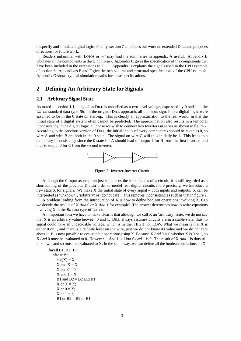
As notedin section1.1, a signalin DILL is modelledasa two-level voltage,expressedby 0 and1 in theLOTOS standarddatatype Bit. In the original DILL approach,all the input signalsto a digital logic wereassumedto be in the 0 stateon start-up. This is clearly an approximationto the real world, in that theinitial stateof a digital systemoften cannotbe predicted. The approximationalsoresultsin a temporalinconsistency in thedigital logic. Supposewewishto connecttwo Invertersin seriesasshown in figure2.Accordingto thepreviousversionof DILL , theinitial inputsof every componentsshouldbetakenas0, sowire A andwire B areboth in the 0 state. The signalon wire C will thusinitially be1. This leadsto atemporaryinconsistency sincethe 0 statefor A shouldleadto output1 for B from the first inverter, andthusto output0 for C from thesecondinverter.
A B C
Figure2: Inverter-InverterCircuit
Although the 0 input assumptionjust influencesthe initial statesof a circuit, it is still regardedasashortcomingof the previous DILL_In order to model real digital circuits moreprecisely, we introduceanew stateX for signals.We makeX the initial stateof every signal– both inputsandoutputs.X canbeinterpretedas‘unknown’, ‘arbitrary’ or ‘do notcare’. Thisremovesinconsistenciessuchasthatin figure2.
A problemleadingfrom the introductionof X is how to definebooleanoperationsinvolving X. Canwedecidetheresultsof X And0 or X And1 for example?Theanswerdetermineshow to write equationsinvolving X in theBit datatypeof LOTOS.
An importantideawe have to makeclearis thatalthoughwe call X an‘arbitrary’ state,wedo not saythatX is anarbitraryvaluebetween0 and1. DILL alwaysassumescircuitsarein a stablestate,thusnosignalcouldhave anundecidablevoltage,which is neitherHIGH nor LOW. Whatwe meanis thatX iseither0 or 1, andthereis a definitelevel on the wire, just we do not know its valueandwe do not careaboutit. It is now possibleto evaluatebit operationsusingX. BecauseX And0 is 0 whetherX is 0 or 1, soX And0 mustbeevaluatedto 0. However, 1 And1 is 1 but 0 And1 is 0. Theresultof X And1 is thusstillunknown,andsomustbeevaluatedto X. In thesameway, wecandefineall thebooleanoperationsonX:
forall B1, B2: Bitofsort Bit
not(X) = X;X andX = X;X and0 = 0;X and1 = X;B1 andB2 = B2 andB1;X or X = X;X or 0 = X;X or 1 = 1;B1 or B2 = B2 or B1;
3

Otheroperationscanbederivedfromthenot, and, or operations,justasfor theusualtwo-valuebooleanoperations:
anandb = not(aandb);anorb = not(aor b);axor b = (a andnot(b))or (not(a)andb);
NormallyweuseX astheinitial stateof all signals,but it canalsobeusedastheinputstateof asignalat any time. In the later case,X alwaysmeans‘do not care’. Hardwareengineersarefamiliar with thisidea,andit makesDILL specificationmoreflexible.
2.2 Impact on Modelsof BasicGates
The modelsof basic logic gatesneedto be changedas a consequenceof introducingthe X. Perhapssurprisingly, the modifiedspecificationsaremuchsimplerthanthe originals. In the previous versionofDILL , every processmodellinga basiclogic gatehad two auxiliary processesdealingrespectively withinitial outputsandlater outputs. The new versiononly hasoneauxiliary processsinceinitial statesarehandledby thebit operations.Taketheone-inputlogic gateasexample:
processLogic1 [Ip, Op] (BOp : BitOp) : noexitLogic1Aux [Ip, Op] (BOp,X of bit, X of bit)
where
processLogic1Aux [Ip, Op] (BOp: BitOp, BIn, BOut : Bit) : noexitIp ? BInNew : Bit;Logic1Aux[Ip, Op] (BOp,BInNew, BOut)
(let BOutNew : Bit = Apply (BOp,BIn) in
[(BOut eqX) and(BOutNew eqX)]Op? BOutNew : Bit[BOutNew neX];Logic1Aux [Ip, Op] (BOp,BIn, BOutNew)
[(BOutNew neX) and(BOutNew neBOut)]Op ! BOutNew;Logic1Aux [Ip, Op] (BOp,BIn, BOutNew)
)endproc (* Logic1Aux*)
endproc (* Logic1*)
Themainpointsto noteaboutthisspecificationare:
all theinputandoutputsignalsareinitializedto X
if thecurrentinputvaluesdonot fully determineanoutput,theoutputcanbeanarbitrarybut specificvalue(0 or 1)
this is necessaryto describesequentialcircuitscorrectly(sincethey mayhave feedback)
withoutthischange,if anoutputof X weregivenit mightbefedbackto theinput; theoutputsmightthereforestick at X (theequivalentof livelock) insteadof settlingon definitevalues. An exampleis our designof themaster-slave JK flipflop (see[4] for circuit diagram),without suchchange,theoutputQ andQbarcannever settledown on1 or 0 statenomatterhow JandK change.)
4

3 Multi-Bit Signalsand Buses
In digital circuits, it is quite usualthat somerelatedsignalsareregardedasa whole. For example,in acomputersystema groupof 16 bit datasignalscouldbeseenasonesignalcarriedby a databus. We callsucha signalconsistingof morethanonebit signalsa multi-bit signal. Using the term from computerhardware,wereferto awire carryingthemulti-bit signalasabus. Multi-bit signalandbusis anabstractionfrom therealphysicalworld in which thereexist only individual one-bitsignals,eachcarriedby a wire.Many hardwaredescriptionlanguagesprovide datatypesto supportthis abstractionin orderto simplifyspecificationand also conform to what hardwareengineersare usedto. For example, VHDL (VLSIHardwareDesignLanguage[3]) definesan‘array of bits’ to representmulti-bit signals.Thenew versionof DILL is alsoableto specifymulti-bit wires(buses)andmulti-bit signals,whicharebasedonthedifferentstylesof specification.
3.1 Macrosfor Multi-Bit Wir esAnd Signals
In thestructuralspecification(seesection5), wehave two macrosMWireandMCompto specifymulti-bitwires (buses)andcomponentswith suchwires. As will be seenlater, multi-bit wires areexpandedtoindividual wireseachcarryinga one-bitsignal. Similarly, multiple componentsareexpandedto severalindividualcomponents.
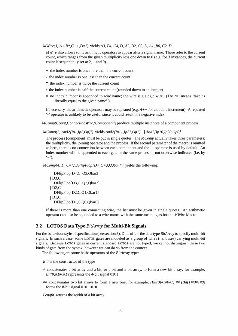
MacroMWire(Count,‘WireList’) is usedfor specifyinga multi-bit wire of width ‘Count’. For instance,Mwire(8,‘D’) representsan8-bit databusD. MWire is supportedby them4macrolibrary, beingultimatelytranslatedinto a LOTOS specification.For theexampleof MWire(8,‘D’), theLOTOS specificationwill havegatesD7, D6, D5, D4, D3, D2, D1, D0.
Macro MComp(Count,ConnectingWire,‘Component’) representsa group of componentswith simi-lar architecture. Supposethat the LOTOS processDFlipFlop[D,C,Q,Qbar] modelsa D-type flip-flop.MComp(4,C=,‘DFlipFlop[D,C=,Q,Qbar]’)will correspondto a 4-bit D-typeflip-flop with a clock signalcommonto its four one-bitflip-flops. Like MWire, macroMCompendsupgeneratingLOTOS. The4-bit Dtypeflip-flop will appearas:
DFlipFlop[D3,C,Q3,Qbar3]CDFlipFlop[D2,C,Q2,Qbar2]
CDFlipFlop[D1,C,Q1,Qbar1]
CDFlipFlop[D0,C,Q0,Qbar0]
MCompandMWirearealwaysusedtogether. For the4-bit D-typeflip-flop, aDILL processrepresentingit will be:
processDFlipFlop4[MWire(4,D),C,MWire(4,‘Q,Qbar’)]: noexitMComp[4,C=,‘DFlipFlop[D,C=,Q,Qbar]’)
endproc
As wehave seen,thecombinationaluseof thetwo macrosresultsin very compactDILL specifications.Althoughthesetwo macrosarejustshorthandsfor theone-bitform of LOTOS specification,they provideaconcisespecificationthatincorporatesconventionalhardwareideas.
Besidestheessentialfunctionillustratedabove,MWireandMComparedesignedfor flexible intercon-nectionof componentsin largecircuitswith repeatedstructure.Below we give someexamplesto explainhow they areused.
MWire(Count,‘WireList’)producesmultiple instancesof wires:
MWire(4,‘X,Y’) yieldsX3,Y3,X2,Y2,X1,Y1,X0,Y0. X andY canberegardedas4-bit busesthatareexpandedinto 4 one-bitwires.
If thereis more thanonebus in the bus list, singlequotesmustbe put roundthe list. The indexnumberafter thewire namesdecreasesby 1 from theindex of MSB (Most SignificantBit) to LSB(leastSignificantBit).
5
MWire(3,‘A+,B*,C++,D=’) yieldsA3,B4,C4,D, A2,B2,C3,D, A1,B0,C2,D.
MWirealsoallowssomearithmeticoperatorsto appearafterasignalname.Thesereferto thecurrentcount,which rangesfrom thegivenmultiplicity lessonedown to 0 (e.g.for 3 instances,thecurrentcountis sequentiallysetat2, 1 and0).
+ theindex numberis onemorethanthecurrentcount
- theindex numberis onelessthanthecurrentcount
* theindex numberis twice thecurrentcount
/ theindex numberis half thecurrentcount(roundeddown to aninteger)
= no index numberis appendedto wire name;the wire is a singlewire. (The ‘=’ means‘take asliterally equalto thegivenname’.)
If necessary, thearithmeticoperatorsmayberepeated(e.g.A++ for adoubleincrement).A repeated‘-’ operatoris unlikely to beusefulsinceit couldresultin anegative index.
MComp(Count,ConnectingWire,‘Component’)producemultiple instancesof acomponentprocess:
MComp(2,‘And2[Ip1,Ip2,Op]’)yieldsAnd2[Ip11,Ip21,Op1] And2[Ip10,Ip20,Op0].
Theprocess(component)mustbeput in singlequotes.TheMCompactuallytakesthreeparameters:themultiplicity, thejoining operatorandtheprocess.If thesecondparameterof themacrois omittedashere,thereis no connectionbetweeneachcomponentandthe operatoris usedby default. Anindex numberwill beappendedto eachgatein thesameprocessif not otherwiseindicated(i.e. by‘=’).
MComp(4,‘D,C=’,‘DFlipFlop[D+,C=,Q,Qbar]’) yieldsthefollowing:
DFlipFlop[D4,C,Q3,Qbar3]D3,CDFlipFlop[D3,C,Q2,Qbar2]
D2,CDFlipFlop[D2,C,Q1,Qbar1]
D1,CDFlipFlop[D1,C,Q0,Qbar0]
If thereis more thanoneconnectingwire, the list mustbe given in singlequotes. An arithmeticoperatorcanalsobeappendedto a wire name,with thesamemeaningasfor theMWireMacro.
3.2 LOTOSData Type BitArray for Multi-Bit Signals
For thebehaviourstyleof specification(seesection5),DILL offersthedatatypeBitArraytospecifymulti-bitsignals.In sucha case,someLOTOS gatesaremodeledasa groupof wires(i.e. buses)carryingmulti-bitsignals. BecauseLOTOS gatesin currentstandardLOTOS arenot typed,we cannotdistinguishthesetwokindsof gatefrom thesyntax,however wecandosofrom thecontext.
Thefollowing aresomebasicoperatorsof theBitArray type:
Bit is theconstructorof thetype
# concatenatesa bit arrayanda bit, or a bit anda bit array, to form a new bit array; for example,Bit(0)#1#0#1representsthe4-bit signal0101
## concatenatestwo bit arraysto form a new one; for example,(Bit(0)#1#0#1)## (Bit(1)#0#1#0)formsthe8-bit signal01011010
Length returnsthewidth of a bit array
6

NatNum changesthebinaryvaluerepresentedby a bit arrayto anaturalnumber
+ addsthevalueof two bit arrays,or onebit arrayanda bit
not,and,nand,... arelogical operators
eq,ne,lt, ... arerelationaloperators
. getsthevalueof a particularbit from a bit array
Set setsthevalueof a particularbit in a bit array
A multi-bit signalrepresentedby BitArray canalsobe treatedasa setof individual one-bitsignals.OperatorsSetand‘.’ allow usto accessany individualbit in a bit array. ThusdatatypeBitArray canbeusedwith bothn-bit andone-bitwires.
We couldcontinueto definea lot of operatorsof BitArray accordingto theneedsof thecircuits to bedefined.For example,if we wishedto definea BCD adder, we might wantto definesomenew operatorsrelatingto BCD operations.
IntroducingthetypeBitArray canresultin moreabstractspecificationsof digital systems,allowing usto ignorethedetailsof how a logic designis implemented.It alsomakesit possibleto useoneprocesstomodelagroupof componentswith thesamebehaviour exceptfor thenumberof inputsand/oroutputs.ForinstanceReg nBB[D,Ck,Q]couldrepresenta registerof any datawidth.
4 Tri-State Components
In the discussionof previous sections,we referredonly to two statesof a signal0 or 1. Although weintroducedthe X state,it just meanseither0 or 1. For a tri-statecomponent,its outputsare in oneofthreestates:normallow-impedanceLow, normallow-impedanceHigh, anda high-impedancestate.Theadvantageof tri-statecomponentsis thattheoutputsof severalsuchcomponentscanbeconnectedtogetherwithout theworry of damageto thecomponents.(Theoutputsof normalcomponentscannotbeconnectedsincethiswould leadto ashortcircuit if onecomponentweretrying to output0 andtheotherto output1.)Tri-stateoutputis especiallyusefulwhenwewantto transferdataamongseveralcomponentsvia abus.Asshown in figure3, theregistersA, B, C andD areconnectedto theregisterG throughBus, theoutputsoftheDecoderdeterminewhich registeris allowedto transferits datato theregisterG .
RegisterG
Register
ARegister
B
RegisterC
RegisterD
ENA ENB ENC END
E
FDecoder
Bus
8 8 8 8
8Clock
Figure3: DataTransferthroughBus
7
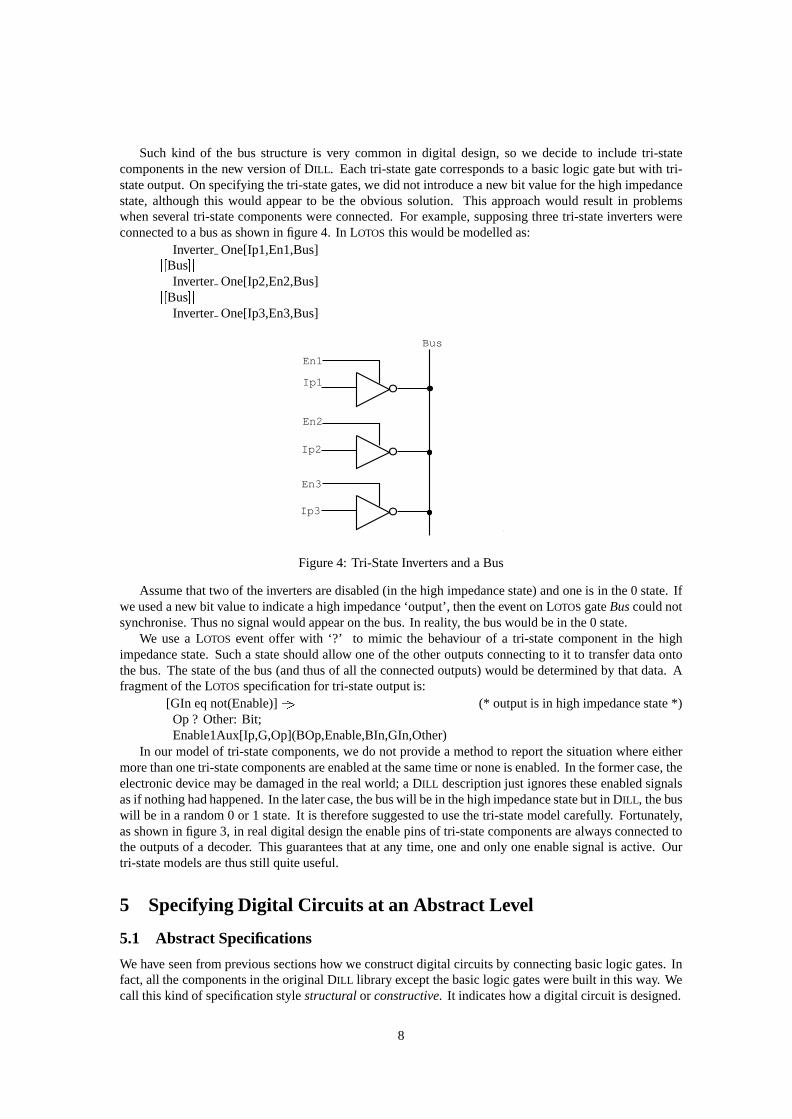
Suchkind of the bus structureis very commonin digital design,so we decideto include tri-statecomponentsin thenew versionof DILL . Eachtri-stategatecorrespondsto a basiclogic gatebut with tri-stateoutput.Onspecifyingthetri-stategates,wedid not introducea new bit valuefor thehigh impedancestate,althoughthis would appearto be the obvious solution. This approachwould result in problemswhenseveral tri-statecomponentswereconnected.For example,supposingthreetri-stateinverterswereconnectedto a busasshown in figure4. In LOTOS thiswouldbemodelledas:
Inverter One[Ip1,En1,Bus]BusInverter One[Ip2,En2,Bus]
BusInverter One[Ip3,En3,Bus]
En1
Ip1
En2
Ip2
En3
Ip3
Bus
Figure4: Tri-StateInvertersanda Bus
Assumethattwo of theinvertersaredisabled(in thehigh impedancestate)andoneis in the0 state.Ifweusedanew bit valueto indicateahigh impedance‘output’, thentheeventonLOTOSgateBuscouldnotsynchronise.Thusnosignalwouldappearon thebus. In reality, thebuswouldbein the0 state.
We usea LOTOS event offer with ‘?’ to mimic the behaviour of a tri-statecomponentin the highimpedancestate.Sucha stateshouldallow oneof theotheroutputsconnectingto it to transferdataontothebus. Thestateof thebus(andthusof all theconnectedoutputs)would bedeterminedby thatdata. Afragmentof theLOTOS specificationfor tri-stateoutputis:
[GIn eqnot(Enable)] (* outputis in high impedancestate*)Op? Other:Bit;Enable1Aux[Ip,G,Op](BOp,Enable,BIn,GIn,Other)
In our modelof tri-statecomponents,we do not provide a methodto reportthesituationwhereeithermorethanonetri-statecomponentsareenabledat thesametimeor noneis enabled.In theformercase,theelectronicdevice maybedamagedin therealworld; a DILL descriptionjust ignorestheseenabledsignalsasif nothinghadhappened.In thelatercase,thebuswill bein thehighimpedancestatebut in DILL , thebuswill be in a random0 or 1 state.It is thereforesuggestedto usethetri-statemodelcarefully. Fortunately,asshown in figure3, in realdigital designtheenablepinsof tri-statecomponentsarealwaysconnectedtotheoutputsof a decoder. This guaranteesthatat any time,oneandonly oneenablesignalis active. Ourtri-statemodelsarethusstill quiteuseful.
5 SpecifyingDigital Cir cuits at an Abstract Level
5.1 Abstract Specifications
We have seenfrom previoussectionshow weconstructdigital circuitsby connectingbasiclogic gates.Infact,all thecomponentsin theoriginalDILL library exceptthebasiclogic gateswerebuilt in this way. Wecall this kind of specificationstylestructural or constructive. It indicateshow a digital circuit is designed.
8

Alternatively, we can usea more abstractstyle to specify our digital circuits. In suchan abstractspecification,we just specifywhat a componentshoulddo ratherthanhow it is implemented.We havesomegoodreasonsto specifydigital logic in thisway:
LOTOSsupportsspecificationsata numberof levels. It is quitenaturalfor usto useit in higher-levelspecification.
In somecircumstancesit is not necessaryfor us to know exactly how a componentis built. Forexample,supposewe want to designan ALU (Arithmetic andLogic Unit) which interactswith agroupof registers.We donot careabouttheconstructionof theregistergroupat thisstage;weonlyneedto know its behaviour from the perspective of the outsideenvironment. We shouldthereforespecifythe registergroupasa blackbox which just describesthe relationshipbetweeninputsandoutputs.
Thereis well-developedhardwaresynthesistheory which provides the possibility to translateanabstractdescriptioninto a concreteimplementationautomatically.
Thevalidationof digital logic designsin DILL is mainlyby simulationatpresent.As wepointedoutearlier, thecurrentsimulationtoolshandlecomplex circuitsspecifiedin thestructuralstylepoorlydueto numerousinternalevents.Oneway to overcomethis problemis to improve theLOTOS tools. Theotherwayis throughabstractspecification.Whenwehaveconfidencein ourdesignfor acomponent,we mayreplaceit by its abstractcounterpartandusetheabstractcomponentin larger circuits. Sothesimulationof thelargercircuitswill beonly relatedto theabstractone. In thisway, weavoid theinternaleventsin thestructuralspecification.
Therearetwo stylesfor specifyingcomponentsin anabstractway: data flow andbehavioural. Theabstractcomponentsin theDILL library arespecifiedin eitherof thesestylesat thespecifier’sconvenience.Severalcomponentshave beenspecifiedin bothstylesto comparethedifferencesbetweenthem.
5.2 Data Flow Style
In thedataflow style,weusetheLOTOSlocaldefinitionoperatorlet...in to describehow inputsignals(data)flow throughthecircuit to producetheoutputs.
SupposewearedescribinganRSlatch(figure5). Themainpartof its specificationis:... (* inputssignalchanged*)
let newdtQ : Bit = dtRnordtQbar,newdtQbar:Bit = dtSnordtQ in
(...) (* outputnew valueof outputsignal*)
R
S
Q
Qbar
Figure5: RSlatch
A fragmentof thespecificationfor a 4-bit adder(figure6) mightbe:... (* inputssignalchanged*)let newdtS: BitArray = (dtA + dtB) + dtC0,
newdtC4: Bit = Carry(dtA,dtB)or Carry((dtA+ dtB),dtC0)in(...) (* outputschangedaccordingto new value*)
9
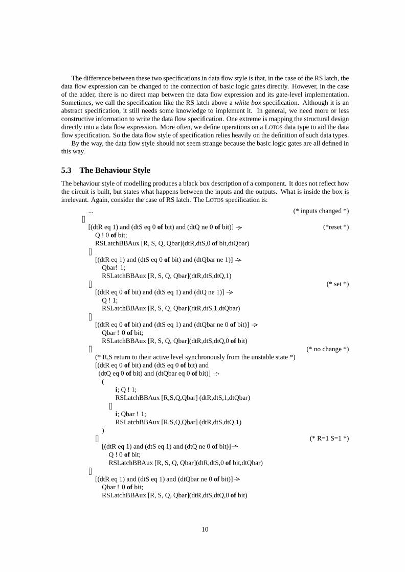
Thedifferencebetweenthesetwo specificationsin dataflow styleis that,in thecaseof theRSlatch,thedataflow expressioncanbechangedto theconnectionof basiclogic gatesdirectly. However, in thecaseof the adder, thereis no direct mapbetweenthe dataflow expressionandits gate-level implementation.Sometimes,we call thespecificationlike theRSlatch above a whitebox specification.Although it is anabstractspecification,it still needssomeknowledgeto implementit. In general,we needmoreor lessconstructiveinformationto write thedataflow specification.Oneextremeis mappingthestructuraldesigndirectly into a dataflow expression.Moreoften,wedefineoperationsona LOTOSdatatypeto aid thedataflow specification.Sothedataflow styleof specificationreliesheavily onthedefinitionof suchdatatypes.
By theway, thedataflow styleshouldnot seemstrangebecausethebasiclogic gatesareall definedinthisway.
5.3 The Behaviour Style
Thebehaviour styleof modellingproducesablackboxdescriptionof acomponent.It doesnot reflecthowthecircuit is built, but stateswhathappensbetweenthe inputsandtheoutputs.What is insidethebox isirrelevant.Again,considerthecaseof RSlatch. TheLOTOS specificationis:
... (* inputschanged*)
[(dtR eq1) and(dtSeq0 of bit) and(dtQ ne0 of bit)] (*reset*)Q ! 0 of bit;RSLatchBBAux [R, S,Q, Qbar](dtR,dtS,0of bit,dtQbar)
[(dtR eq1) and(dtSeq0 of bit) and(dtQbarne1)]Qbar! 1;RSLatchBBAux [R, S,Q, Qbar](dtR,dtS,dtQ,1)
(* set*)[(dtR eq0 of bit) and(dtSeq1) and(dtQne1)]
Q ! 1;RSLatchBBAux [R, S,Q, Qbar](dtR,dtS,1,dtQbar)
[(dtR eq0 of bit) and(dtSeq1) and(dtQbarne0 of bit)]Qbar! 0 of bit;RSLatchBBAux [R, S,Q, Qbar](dtR,dtS,dtQ,0of bit)
(* nochange*)(* R,Sreturnto their active level synchronouslyfrom theunstablestate*)[(dtR eq0 of bit) and(dtSeq0 of bit) and(dtQ eq0 of bit) and(dtQbareq0 of bit)](
i; Q ! 1;RSLatchBBAux [R,S,Q,Qbar](dtR,dtS,1,dtQbar)
i; Qbar! 1;RSLatchBBAux [R,S,Q,Qbar](dtR,dtS,dtQ,1)
)(* R=1S=1*)
[(dtR eq1) and(dtSeq1) and(dtQ ne0 of bit)]Q ! 0 of bit;RSLatchBBAux [R, S,Q, Qbar](dtR,dtS,0of bit,dtQbar)
[(dtR eq1) and(dtSeq1) and(dtQbarne0 of bit)]Qbar! 0 of bit;RSLatchBBAux [R, S,Q, Qbar](dtR,dtS,dtQ,0of bit)
10

Thebehaviour stylefor anRSlatchgivestherelationshipbetweentheinputsandtheoutputs.If R=1,S=0 then the outputsare reset(Q=0, Qbar=1). If R=0, S=1 thenthe outputsareset (Q=1, Qbar=0)and so on. In general,LOTOS guardsare usedto specify the relationshipbetweeninputs and outputs.Note the internalevent i in the ‘no change’state. If the two inputsR, S returnfrom the inactive state(0)synchronouslyto theactivestate(1), theoutputscannotbedecidedby theenvironment;theresultdependsonthespeedof thegatesinsidethecircuit (i.e.thereis aracecondition).Weusetheinternaleventto modelthenon-deterministicbehaviour.
Onemayarguethatthebehaviour styleis not trivial evenfor a simpleRSlatch. This is trueif we readthespecificationsof componentsin theDILL library. Almost every componentspecifiedin thebehaviourstylehasamuchlongerdescriptioncomparedto itsstructuralcounterpart.But in fact,theideaof specifyinga componentin suchstyle is very easy. What makesthe descriptionlook so clumsyis aspectsthat aresimilar in all thecomponentspecifications.For example,a lot of guardsareusedto guaranteethataLOTOS
eventmodelsa changeof signal.Reducingthe complexity of the behaviour style specificationis on the agendaof our future work on
DILL . Onepossiblesolutionmaybethroughaddingmoremacroslike MWireandMCompto givethe‘core’partof thebehaviour. Theother, commonpartof thespecificationcouldbegeneratedautomaticallyduringtheexpansionof themacros.
5.4 SpecifyingCir cuits with Edge-SensitiveSignals
Thereareseveralcomponentsin theDILL librarywhoseinputsor outputsaresensitiveto signaledgesratherthanvaluesof anothersignal.Themostcommonof suchsignalsarerelatedto aclock,i.e.changesof thesesignalsdependon thechangingof a clock. Takethe exampleof anedge-triggeredD flip-flop (figure 7).TheoutputsQ andQbarcanbechangedonly at thenegative-goingtransitionof theclock.
Themethodof specifyingsuchoutputsis somewhatdifferentfrom outputsthatarenot edge-sensitive.Themethodfor specifyingcircuitswithoutedge-sensitivesignalstakestheform:
(* Input1changed,go to next state*)
...
(* InputI changed,go to next state*)
(* Output1changed,go to next state*)
...
(* OutputOchanged,go to next state*)
In this model,every signalis independentof every other. But for circuits thatareedge-sensitive, thismodelshouldbemodifiedto guaranteeall theoutputssensitive to theclockarecorrectlychangedaftertheappropriateclock transition.
(* Input1changed,go to next state*)
...
(* InputI changed,go to next state*)
(* Clockchanged*)(
(* Edge-sensitiveOutput1changed,exit *)
...
(* Edge-sensitiveOutputEchanged,exit *)
11

)
(* NormalOutput1changed,go to next state*)
...
(* NormalOutputNchanged,go to next state*)
Writing specificationsfor edge-sensitivesignalsmustalwaysbedonecarefullytoavoiddeadlock,whichresultsfrom incorrectguardsaftertheclock transition.
5.5 Componentswith Non-FixedNumber of Signals
Sometimesweneeda moreflexible andmoreabstractmodelto representa classof circuits. For example,perhapswe needann-bit registerto representall registersno matterwhat thedatawidthsare. Of coursethereis no suchregister in the realworld. We abstractsucha componentin orderto useit in every casewherewe needa registerbut do not careaboutthewidth, or wherethewidth canbedecidedby theothercomponentsconnectedto it.
The LOTOS datatype BitArray providesa convenientway to specifysucha component.An abstractspecificationof a componentwith a one-bitsignalcanbeeasilychangedto specificationfor n bits. Whatis neededis just changingthecorrespondingsignaltype(from Bit to BitArray) in theparameterlist of theauxiliaryprocess.
Suchcomponentscannotbeconnectedwith someof theothercomponentssinceLOTOS gatesin thesecomponentsrepresentbuseswhichwill carryN-bit signals.However, anordinarygatein othercomponentscancarryonly onebit. n-bit componentsarealwaysconnectedto providea specificationof digital logic atthesystemlevel.
6 CaseStudy: Designinga Sub-CPUin DILL
In this sectionwe will give anexampleto show how to useDILL to designandsimulatea digital system.Designingthedigital systemneedsall thenew featuresweaddedto DILL , suchasmulti-bit signalandbus,tri-statecomponents,abstractcomponentsandso on. The exampledealswith designingpart of a CPU(CentralProcessingUnit) of a simplecomputersystem.We will refer to this partof theCPUassub-CPUin thefollowing text. AppendixD summarisesthemeaningof signalsusedin thisexample.
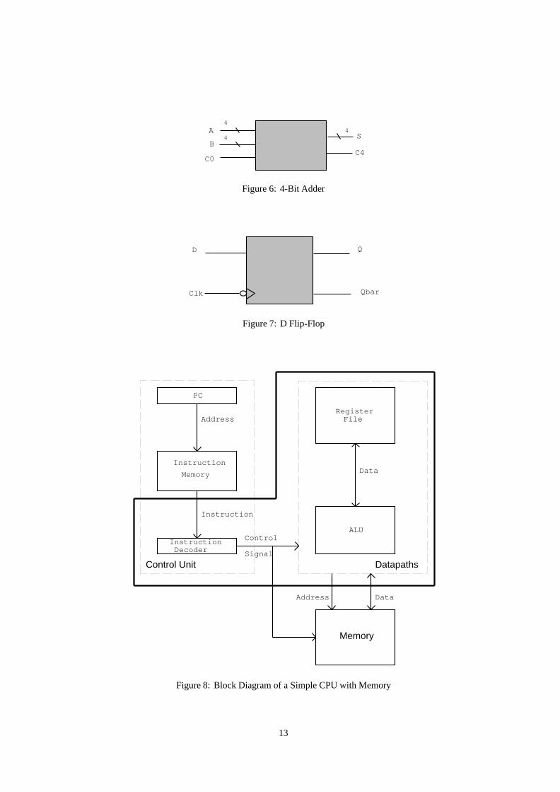
6.1 Structur eof a Typical CPU
As we know, a typical CPUmainly consistsof two parts: thecontrolunit andthedatapaths.Thecontrolunit providesall the necessarycontrol signalsthatactivatethe variousmicro-operationsin the datapathsto performthe specifieddataprocessingtasks. It alsodeterminesthe sequencein which variousactionsareperformed. Generally, the control unit consistsof a programcounter(PC) which providesthe nextinstructionaddressto the instructionmemory. An instructionmemorycontainsseveral instructionsto beexecutedin futuresteps,andacontrollogic whichacceptsaninstructionandyieldsthecontrolsignals.Thedatapathsperformdifferentkindsof dataprocessingtasksaccordingto thedifferentinstructionsfrom thecontrolunit. It is acombinationof a setof registers(termeda registerfile), anarithmeticlogic unit (ALU)andinternalbusesthatprovide pathwaysfor the transferof informationbetweenthe registers,ALU andothercomputercomponents.
A CPUinevitably hasconnectionswith theotherpartsof a computersystem,for examplememoryorI/O interfaceunits. TheCPUprovidesbusesfor transferringcode,dataandcontrol informationbetweenitself andits connectingcomponents.Figure8 showsablockdiagramfor asimpleCPUconnectingwith amemory. Notethateverypartin thefigure,exceptinstructiondecoderandALU, is controlledby thesystemclock,whichwedid notdraw in thefigure. Ourexamplewill bebasedonthis structure.
12
4
44A
B
C0
S
C4
Figure6: 4-Bit Adder
D
Clk
Q
Qbar
Figure7: D Flip-Flop
Address
PC
Instruction
Memory
Instruction Decoder
Instruction
Control
Signal
Data
DataAddress
ALU
Control Unit
Memory
RegisterFile
Datapaths
Figure8: Block Diagramof a SimpleCPUwith Memory
13

6.2 The DesignObjectivesof the Sub-CPU
Our sub-CPUconsistsof thedatapathsandthecontrol logic of thecontrolunit, which areincludedin theboldbox in figure8. This is a goodstartfor usto definetheobjectivesof designingthesub-CPU.
Thesub-CPUis a single-cycle CPU,which meansfetchingandexecutingan instructionshouldbefinishedin a singleclockcycle.
Thesub-CPUis a partof a 4-bit computer, whichmeansthewidthsof dataregisters,databusesandthememoryunitsareall 4 bits.
Therearefour dataregistersin thedatapaths,namedR0, R1,R2,R3,andtwo flag registers,namedFlag0,Flag1.
Theseregistersloadtheir inputsona positivetransitionof theclocksignal.
TheALU performstwo operations:additionof two valuesandcomparisonof two values.
Theinstructionsetof thesub-CPUincludes4 instructions:1
– LoadDR,SALoadthevalueresidingin a memoryunit whoseaddressis specifiedby registerSA into registerDR.
– StoreSA,SBStorethevalueresidingin registerSBto amemoryunit,whoseaddressis specifiedin registerSA.
– Add DR, SA,SBAdd two valuesresidingin registersSA andSB,sendingthe sumto registerDR andthecarryto Flag1.
– CmpSA,SBComparethetwo valuesin registerSA, SB; if they areequal,theFlag0is setto 1otherwisesetto 0.
NotethattheregistersDR, SA, SB in theabove instructionsreferto any oneof R3,R2,R1,R0.
Thestructureof aninstructionis shown in figure9, in which:
– DR is theDestinationRegister.
– SA is theSourceA register.
– SBis theSourceB register.
– Opcoderepresentstheoperationto beexecuted.
00Comparetwo valuesin registerSA andregisterSB.01Storeavaluein registerRB to a memoryunit, whoseaddressis in registerSA.10Loada valuefrom a memoryunit, whoseaddressis in registerSA, to registerDR.11 Add the valuesin SourceA registerandSourceB register andsendthe sum to theDestinationRegisterDR.
Opcode DR SA SB
01234567
Figure9: TheStructureof anInstruction
For anexampletheinstructionAddR3,R1,R2will be in thefollowing binaryform: 11110110. InDILL , it is representedby a valueof typeBitArray bit(1)#1#1#1#0#1#1#0.
If the numberof operandsis lessthan3, the unusedbits canbe filled with either1s or 0s. In thesimulationdiscussedin this report,we feedeachunusedbit with 0. For instructionLoadR3,R2theDILL representationwill bebit(1)#0#1#1#1#0#0#0. Notetheunusedbits herearebit 1 andbit 0.
1Thefinal instructionsetwill contain5 instructions.Seesection6.3.2.
14
The connectionbetweenthe sub-CPUandmemoryis achieved throughaddressbus BusAorMArr,two databusesDtIn andBusBorDtOutandcontrolsignalMW (MemoryWrite).
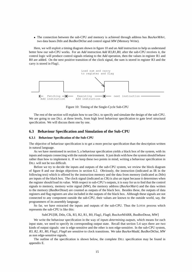
Here,wewill exploit a timing diagramshown in figure10andanAddinstructionto helpusunderstandbetterhow our sub-CPUworks. For anAdd instructionAdd R3,R1,R0, after thesub-CPUreceivesit, thecontrol logic will producecontrolsignalsrelatingto theAddoperation,thenthevaluesin registerR1 andR0 areadded.On thenext positive transitionof theclock signal,thesumis storedin registerR3 andthecarryis storedin Flag1.
Fetching Executing Add instruction Add instruction
next instruction
Load sum and carryto register and flag
Figure10: Timing of theSingle-CycleSub-CPU
Therestof thesectionwill explain how to useDILL to specifyandsimulatethedesignof thesub-CPU.We aregoing to useDILL at threelevels, from high level behaviour specificationto gatelevel structuralspecification.We will discussthemoneby one.
6.3 Behaviour Specificationand Simulation of the Sub-CPU
6.3.1 Behaviour Specificationof the Sub-CPU
Theobjective of behaviour specificationis to geta moreprecisespecificationthanthedescriptionwrittenin naturallanguage.
As wehave mentionedin section5, a behaviour specificationyieldsa blackboxof thesystem,with itsinputsandoutputsconnectingwith theoutsideenvironment.It justdealswith how thesystemshouldbehaveratherthanhow to implementit. If wekeepthesetwo pointsin mind,writing a behaviour specificationinDILL will notbetoodifficult.
Beforewe try to decidethe inputsandoutputsof the sub-CPUsystem,we review the block diagramof figure 8 andour designobjectives in section6.2. Obviously, the instruction(indicatedas IR in thefollowing text) which is offeredby theinstructionmemoryandthedatafrom memory(indicatedasDtIn)areinputsof theblackbox. Theclocksignal(indicatedasClk) is alsoaninputbecauseit determineswhentheregistershouldloadits value.With respectto sub-CPU’soutputs,it is easyfor usto find thatthecontrolsignalsto memory, memorywrite signal(MW), the memoryaddress(BusAorMarr) andthe datawrittento thememory(BusBorDtout) arecountedasoutputsof theblackbox. Besidesthese,theoutputsof dataregistersandflagregistersarealsoincludedin theoutputsof theblackbox. Althoughthesesignalsarenotconnectedto any componentoutsidethe sub-CPU,their valuesareknown to the outsideworld, say, theprogrammersof its assemblylanguage.
So far, we have extractedthe inputs and outputsof the sub-CPU.Thus the LOTOS processwhichrepresentsthesub-CPUis like this:
SubCPU[IR,DtIn, Clk, R3,R2,R1,R0,Flag1,Flag0,BusAorMARR,BusBorDtout,MW]
We write thebehaviour specificationin theway of inputsdeterminingoutputs, which meansfor eachinput state,we needto specifyits correspondingoutputstate. Recall thatsection5.4 saystherearetwokindsof outputsignals:oneis edge-sensitive andtheotheris nonedge-sensitive. In thesub-CPUsystem,R3, R2, R1, R0, Flag1, Flag0aresensitive to clock transitions.We takeBusAorMadd, BusBorDtOut, MWasnonedge-sensitivesignals.
The outline of the specificationis shown below, the completeDILL specificationmay be found inappendixE.
15

Signalon IR is changed;go to thenext state
SignalonDtIn is changed;go to thenext state
SignalonClk is changed;([ Clock signalis from 0 to 1 ]([Is a StoreInstruction]
go to thenext state(* storeinstructiondoesnotyield any edge-sensitivesignal*)
[Is a LoadInstruction]LoadthedataonDtIn to thedestinationregister;go to thenext state
[Is anAdd Instruction](Loadthesumof sourceA registerandsourceB registerto thedestinationregister;
Loadthecarryto theflag1register)
go to thenext state
[Is a CmpInstruction]Loadtheresultof comparisonof sourceA registerandsourceB registerto flag0register;go to thenext state
)
[ Clock signalis not from 0 to 1]goto thenext state
)
[Is a Storeinstruction]SignalonMW changesto 1;go to thenext state
[Is a Loador Add or Cmpinstruction]SignalonMW changesto 0;go to thenext state
DataonBusAorMArr changesto thevalueof sourceA register;go to thenext state
DataonBusBorDtOutchangesto thevalueof sourceB register;go to thenext state
6.3.2 Simulating the behaviour specification
The simulation tool hippo is utilized in the simulationof the designof the sub-CPU.Inspectingtheinstructionsetof thesub-CPU,it is evidentthatall theoperationsarebasedonregisters,namelyeitherthe
16

actualoperandor the addressof a memoryunit in which the actualoperandresidesis in a dataregister.Sowe choosea Load instructionasthefirst instructionto besimulated.For instructionLoadR0,R1. Itsbinaryform is 10001000,in DILL , representedby bit(1)#0#0#0#1#0#0#0of typeBitArray.
Thefollowing is a fragmentof theexecutionpathof theinstruction:
0 START1 IR !(((((((Bi t( 1) # 0) # 0) # 0) # 0) # 1) # 0) # 0)2 MW !03 Clk !04 Clk !1
Thefirst stepfeedstheLoad instructionto theIR. Steps3 and4 modelthepositive transitionof clocksignal.Accordingto ourspecification,we intendthattheMW signalshouldbechangedto 0 becauseonlytheStore instructioncansetit to 1. At thesametime, thememoryaddresswhich is containedin registerR1 shouldappearon BusAorMArr. This simulationpathshows thatthesignalonMW is just asexpectedbut thememoryaddressdoesnot appearon thebus. This is becausethevaluein R2 is anarbitraryvalue,soa definitememoryunit cannotbeaddressed.2
We know thatin our instructionset,all valuesin registerscanonly comefrom memory. Theproblemis thatwe cannotload the memoryaddressto register, becausetheseaddressesshouldalsocomefrom amemoryunit. Soaftera coupleof stepsof simulation,we find ourselvesin a dilemma.This indicatesthatthereis a shortcomingin theoriginal designof the instructionset. We needanotherinstructionto loadavalueto registerotherthanfrom memory.
We adda new load instructionwhich loadsan immediateoperandto a given register. For example,LoadR0,0000loads0 to registerR0. Theoperandvaluecomesfrom theinstructiondirectly. Accordingly,the instructionsetwill containfive instructionsandthe instructionformat is alsochangeda little. Noweachinstructionwill have 9 bits andthehighestbit indicateswheretheoperandcomesfrom, if it is 1, theoperandwill comefrom the instruction,otherwisefrom a memoryunit. The other8 bits have the samemeaningasthepreviousdefinition.
After changingthe specificationto include the new instruction,we simulatethe execution of thefollowing instructionsequence:
Load R0,0000Load R1,0011Load R2,1110Load R3,0011Add R0,R1,R2Cmp R0,R2Cmp R1,R3Load R3,0000Store R3,R1Load R2,R3
Theexecutionpathfor thefirst Load instructionlookslike:
0 START1 IR !((((((((B it (1) # 1) # 0) # 0) # 0) # 0) # 0) # 0) # 0)2 MW !03 Clk !04 Clk !15 R0 !(((Bit(0) # 0) # 0) # 0)6 BusAorMAr r !(((Bit(0 ) # 0) # 0) # 0)7 BusBorDtO ut !(((Bit( 0) # 0) # 0) # 0)
The first stepfeedsthe instructionLoad R0,0000to IR. Sinceit is a Load instruction,the MW ischangedto 0 (MW !0 Memorywrite disable).After thepositive transitionof clock signal,thevaluein R0
2In thebehaviour specificationof thesub-CPU,we assumethat if thevaluein registeris anarbitrarynumber, thecorrespondinginstructionwill beneglected.SeeappendixE.
17

is changedto 0 (R0! 0). Thedataon BusAorMArr andBusBorDtOutarealsochangedaccordingto theLoadinstruction.Becausethechangesappearbetweentheexecutionof thecurrentinstructionandfetchingthenext instruction,they will not affect theexecutionof eitherthecurrentinstructionor thenext one. Bynow, thefirst instructionhasbeenexecutedcorrectly, wemaycontinueto thesecondone.
Thewholeexecutionpathof theabove instructionsequenceis in AppendixG.
6.4 Structural Specificationand Simulation of the Sub-CPU
6.4.1 Structural Specificationof the Sub-CPU
The structuralspecificationspecifiesthe structuraldesignof the sub-CPU.We will not detail the designprocessbut immediatelygive ablockdiagram(figure11)here.
Opcode Dr SA SB
2−4
Decoder
2−4
Decoder
2−4
Decoder
G SA SBInstruction
Decoder
RW
Clk
G
SA
SB
R3
R2
R1
R0
BusA BusBMA DtOut
MW
Register
File
Memory
1−2
Demulplexer
1−2
Demulplexer
0 1 0 1
AddA AddB ComA ComB
Comparator Adder
Zero Carry Sum
Flag0 Flag1
Clk CMP Clk ADDMul 2−1
Mul 2−1
MorF
LI
3 2 2 2
44 4
44
4
4
4
2
2
4
4
4
4
4
10
10
RegIn
RW MW
MorF
LI
ADD
CMP
AorC
AorC
Figure11: Block Diagramof theSub-CPU
The structuralspecificationis achieved by connectingcomponentswith the LOTOS paralleloperator.We canfirst look for thecomponentsin theDILL library. If we cannotfind anappropriateone,a new oneshouldbewritten.
In thesub-CPU,theinstructiondecoderis a specificcomponentin thedesign;weneedto write a newprocessto specifyit. It is written in a behaviour style,becausewedonotwantto introduceinternaleventsduringthesimulation. Thedecoders,multiplexersanddemultiplexersin figure11 canbeeasilyfoundinDILL . Noticethatall four registersareconnectedto bothBusAorMArr andBusBorDtOut,soweneedtwo
18
tri-statecomponents,Wealsoneed4-bit registercomponentsfor dataregisters,and1 bit registeror flip-flopfor flagregistersof oursub-CPU.All thesecomponentsarespecifiedin theDILL library.
Sowhatweneeddois to write anew componentfor theinstructiondecoderin thebehaviour style,andthenconnectall thecomponentsin anappropriateway.
Thecompletespecificationcanbefoundin appendixF.
6.4.2 Simulation of the Structural Specification
Theobjective of simulatinga structuralspecificationis to look for designdefectsin a digital circuit. Bycomparingtheexecutionpathsof behaviour andstructuralspecifications,we will know whethera designsatisfiesits behaviour requirements.
Actually, beforeweobtainedthefinal versionof thestructuralimplementationof thesub-CPU,wehadseveraldesignswhichcontainedbugs,thatwerediscoveredduringsimulation.For example,originally, weusedD flip-flopsto representflags.After executingthesameinstructionsequenceasusedin thesimulationof thebehaviour specification,we foundthebehaviour of flagsaredifferent. Hereis thesimulationpathafterexecutiontheinstructionLoadR0,0000.
0 START5 IR8 !16 IR7 !17 IR6 !08 IR5 !09 IR4 !0
10 IR3 !011 IR2 !012 IR1 !013 IR0 !018 MW !052 Clk !053 Clk !154 Flag1 !055 R03 !056 R02 !057 R01 !058 R00 !059 BusAorMAr r3 !060 BusAorMAr r2 !061 BusAorMAr r1 !062 BusAorMAr r0 !063 BusBorDtO ut3 !064 BusBorDtO ut2 !065 BusBorDtO ut1 !066 BusBorDtO ut0 !0
Herewejust list externalevents(correspondingto theinputsandoutputsof theSub-CPU)andomit allthe internalevents(correspondingto the internalconnectionsbetweencomponents),so thestepnumbersabove are not continuous. Note that the changeof flag1 in event 54 did not appearin the behaviourspecification.Actually, in thestructuraldesignevery instructionmayinfluencethestateof flags,but in thebehaviour specificationonly AddandCmpcanchangetheflags. This suggeststhat thesimpleD flip-flopis nota suitablecomponentto representflags.Finally wereplaceit with a 1 bit registerwith loadcontrol.
After simulatingthemodifieddesignandcomparingits executionpath(in appendixG)with thatof thebehaviour specification,wefind they aresameandsatisfyourselvesthatthis timewegetaproperdesign.
6.5 Gate-Level Specificationand Simulation
Thegatelevel specificationisalsoakindof structuralspecification,but replacingeverycomponentspecifiedin anabstractwaywith aconcreteone.It guaranteesthatadigital designcanbeimplementedbyconnecting
19
ordinarybasiclogic gates,suchasAND,OR,NOT gates.In ourdesignof thesub-CPU,exceptfor theinstructiondecoder, thecomponentsweusedin theprevious
level all have their gatelevel counterpartsin our DILL library. Moreover, all thesecomponentshave beensimulatedbeforethey areput into thelibrary. Sowhatweshoulddoat this level of specificationis trivial:write a structuralspecificationfor the instructiondecoderandsimulateit, finally, replaceall theabstractcomponentswith their gatelevel specification.
6.6 Conclusionof the CaseStudy
Fromaboveexample,wemaygetsomeexperienceof designingdigital logic in DILL . In general,thedesignprocesscanbedividedinto severalsteps:
1. Specifyingthedesignobjectivesof thedigital logic in thebehaviour styleandsimulatingit. In thisstep,we aim at gettinga precisespecificationof thedigital system,andfinding possibledefectsinthedesignrequirements.
2. Specifyingall thecomponentswhichareselectedto build thedigital systemin anabstractstyleandsimulatingthem.Thisstepmaybeomittedif thesecomponentsarealreadyin theDILL library.
3. Specifyingthedigital systemin thestructuralstyle,this is achievedby connectingthecomponentsspecifiedin thesecondstepin anappropriateway. Simulatingthespecificationto seeif it satisfiesthedesignobjectivesof thefirst step.
4. Specifyingthecomponentsselectedin thesecondstepat thegatelevel andsimulatingthem.If thesecomponentsarealreadydefinedby DILL , thestepmaybeomitted.
5. Replacingall theabstractcomponentsin thestructuralspecificationwith theirgatelevel componentsto getagatelevel implementation.
7 Conclusionsand Futur eWork
7.1 Conclusion
In this technicalreportwe have describedthe improvedversionof DILL . The main contentsof the newversioncanbesummarisedas:
ThenecessaryLOTOS datatypesfor hardwarespecificationareprovided:
– standardLOTOS datatypesandextensionsfor modellingone-bitsignals
– BitArray for modellingmulti-bit signals
Digital signalsaremodelledastwo-level voltages,but specifiedusingthreesignalstates:0 for logic0, 1 for logic 1, andX for either0 or 1.
LOTOSgatesuseeitherone-bitwiresor n-bit buses.
The modelof basiclogic gateshasbeenchangedslightly from the original DILL becauseof theintroductionof theX initial parameter. Thenew modelhasa simplerform thantheold one.
New m4macroshave beendefinedfor multi-bit wires.
Tri-statecomponentsarenow availablein thelibrary.
Largercircuitscanbespecifiedin threestyles:
– structuralstyle,connectingsimplercomponentsby LOTOSparallelexpressions
20

– dataflow style, usingLOTOS local definitionsto specify the relationshipbetweeninputsandoutputs
– behaviour style,specifyingthebehavioural propertiesof a component
Throughthe work of the previous DILL version,we have acquiredsomeexperienceof usingLOTOS
for gate-level specification.We have now specifiedsomedigital componentsat anabstractlevel, andfindLOTOS alsoquitesuitablefor higher-level specification.Throughthecasestudyof thesub-CPU,we havegainedmoreconfidencein thesuitabilityof LOTOSfor specifyingandanalysingdigital logic, especiallyforlarger-scaledigital circuits.
7.2 Futur ework
We planfuturework onDILL to includethefollowing:
A morefriendly interfacefor theuserwill bedesigned.As wementionedbefore,thereis only athinlayerabove LOTOSto supporttheuseof DILL . Thereis still a lot of work to bedoneondevelopingabetterinterface.
A simplerapproachfor behaviour specificationof digital circuitswill beinvestigated.As seenin thecasestudyof designingthe sub-CPU,the behaviour specificationhasmuchlongercodesthanthestructuralone.Writing suchspecificationswouldbesomewhatdifficult for hardwareengineers.
Thesimulationtoolsoughtto beimprovedsothat internaleventsaretransparentto DILL users.Anidealtool shouldhave thecapabilityto displaytheoutputsof adigital circuit soonafterits inputsaregiven.
Wewill workonamodelfor specifyingtimingpropertiesof digital logic. ThecurrentLOTOSstandardhasno time capabilities,andtherearevery limited tools to supporttimed specificationin standardLOTOS. DILL currentlyrefersonly to the functionalaspectsof digital logic. But in futurework onDILL , wehopeto investigatetiming propertiesbecausethey areimportantin many logic designs.
Equivalencecheckingbetweendifferent levels of specificationshouldalso be takeninto accountin futurework. As seenin our casestudyof the sub-CPU,we have not provedthat the structuralspecificationof thedesignsatisfiesthebehaviour requirements.
Acknowledgements
Ji He gratefullyacknowledgesfinancialsupportfor this work from theSino-BritishFellowshipTrustandtheUniversityof Stirling. Mr. FrankR. Kelly kindly drew thediagramsin appendixC. Mr. Ian R. Wilsonhelpedby carefullyreadinga draftof thereport.
References
[1] George A.McCaskill andGeorge J. Milne. Hardwaredescriptionandverificationusing the circal-system. TechnicalReportHDV-24-92, Deparmentof ComputerScience,University of Strathclyde,UK, June1992.
[2] G.J.Milne.Modelingdigitla hardwarein a processalgebra.TechnicalReportCIS-95-010,Universityof SouthAustralia,Schoolof ComputerandInformationScience,May 1995.
[3] IEEE.VLSIHardwareDesignLanguage. IEEE1076.Institutionof ElectricalandElectronicEngineersPress,New York, USA, 1992.
[4] RichardO. Sinnott.Thedevelopmentin LOTOSof digital logic specifications.Master’s thesis,Depart-mentof ComputingScienceandMathematics,Universityof Stirling, UK, March1993.
21

[5] KennethJ.Turner. LOTOS– A practicalFormalDescriptionTechniquefor OSI. In InternationalOpenSystems87, volume1, pages265–279.OnlinePublications,London,March1987.
[6] KennethJ.Turner. An engineeringapproachto formalmethods.In AndreA. S.Danthine,GuyLeduc,andPierreWolper, editors,Proc.ProtocolSpecification,TestingandVerificationXIII , pages357–380.North-Holland,Amsterdam,Netherlands,June1993.Invitedpaper.
[7] KennethJ.Turner, editor. UsingFormalDescriptionTechniques—AnIntroductionto ESTELLE, LOTOS
andSDL. Wiley, New York, January1993.
[8] KennethJ. Turner. Exploiting the m4 macrolanguage.TechnicalReportCSM-126,DepartmentofComputingScienceandMathematics,Universityof Stirling, UK, September1994.
[9] KennethJ. TurnerandRichardO. Sinnott. DILL : Specifyingdigital logic in LOTOS. In RichardL.Tenney, Paul D. Amer, andM. Umit Uyar, editors,Proc. Formal DescriptionTechniquesVI, pages71–86.North-Holland,Amsterdam,Netherlands,1994.
22

A LOTOSSyntaxand m4Built-in Commands
ThisappendixgivesselectedLOTOS syntaxin table1 andm4built-in commandsin table2.
Notation Meaning
(* text *) a commentstop a behaviour thatdoesnothing(no furtheraction)exit a behaviour thatimmediatelyterminatessuccessfullyexit (results) successfulterminationwith resultvaluesgate a ‘port’ at whicheventoffersmaysynchronisegate! value anoffer to synchroniseonagivenvaluegate? variable: sort anoffer to synchroniseon any valueof the givensort,binding
theactualvalueto thegivenvariablenamegate! ... ? ... [predicate] aneventoffer with a predicateonvaluessynchronisedprocessname[gates](parameters):
noexit := behavioura namedprocessabstractionwith givengatesandvalueparam-eters,but no termination(e.g.it repeatsindefinitely)
processname[gates](parameters):exit (results):= behaviour
aprocessthatterminatessuccessfullywith thegivenresultsorts
name[gates](parameters) aninstantiationof a namedprocessoffer ; behaviour prefixesaneventoffer to somebehaviour (‘follo wedby’)[guard] behaviour offersbehaviour only if theguardconditionis satisfied(‘if ’)behaviour1 behaviour2 offersa choicebetweentwo behaviours(‘or’)behaviour1 behaviour2 allows thesecondbehaviour to occurif thefirst behaviour ter-
minatessuccessfully(‘enables’)exit (results) successfulterminationwith export of resultvalues
acceptdeclarationsin behaviourbehaviour1 behaviour2 allowsthesecondbehaviour to disruptthefirst behaviour unless
this terminatessuccessfullyfirst (‘disabledby’)behaviour1 behaviour2 allowstwo behavioursto run in parallel,but fully synchronised
on theirevents(‘synchronisedwith’)behaviour1 behaviour2 allows two behaviours to run in parallel,but with independent
occurrenceof their events(‘interleavedwith’)behaviour1 gates behaviour2 allows two behaviours to run in parallel,synchronisingon all
eventsat thegivengates(‘synchronisedongateswith’)
Table1: SelectedLOTOS Syntax
23

Build-in Command Description
#... ignorecommenttext up to andincludingthenew linechangequote(left,right) definequotecharactersasleft andright(insteadof ‘...’)define(name,text) definemacronameto be textdivert(streamnumber) divert futureoutputto streamstreamnumber(1 to 99), thede-
fault of 0 is standardoutputdivnum(streamnumber) expandto currentlyactive diversionnumberdnl deleteup to newline, generallyto prevent extra white spacein
macroeval(expression) expandto resultof numericexpression;thearithmeticandlogi-
cal operatorsareessentiallythoseof Cifdef(‘name’,deftext,undeftext) if macroname(quotedto preventexpansion)is defined,expand
to def text otherwiseundefnextifelse(text1,text2,eqtext,netext) If text1 and text2 areequalstrings,expandto eq text otherwise
ne text; conditionsmayberepeatedinclude(file name) expandto contentsof file nameincr(number) expandto number+1index(string1,string2) expandto positionin string1wherestring2occurs(0 is start,-1
meansnot found)len(string) expandto lengthof stringsubstr(string,position,number) expandto string from position(0 is start)for numbercharacters
(defaultto endof string)translit (string,from,to) expandtostringwith fromcharactersreplacedbycorresponding
to characters(or deletedif thereis nocorresponding)undefine(‘name’) deletedefinitionof name(quotedto preventexpansion)undivert(streamnumber,...) retrievetext fromdiversionstreamnumber(all diversionsasde-
fault) andappendto currentdiversion(usuallystandardoutput)
Table2: Selectedm4Built-in Commands
24
B The DILL Library
Tables3 to 15 summarisethe componentsavailablein theDILL library. In the tables,‘WB’ in the nameof componentsrefersto a White Box (extensional)styleof specification,while ‘BB’ meansa Black Box(intensional)style. In all othercases,anexplicit structuralstylehasbeenfollowed.Thedifferencesamongthesethreestylesarediscussedin section5.
Library Component MeaningAnd2[Ip1,Ip2,Op] 2-inputAndAnd3[Ip1,Ip2,Ip3,Op] 3-inputAndAnd4[Ip1,Ip2,Ip3,Ip4,Op] 4-inputAndAnd8[MWire(8,Ip),Op] 8-inputAndInverter[Ip,Op] Not, InverterNand2[Ip1,Ip2,Op] 2-inputNot AndNand3[Ip1,Ip2,Ip3,Op] 3-inputNot AndNand4[Ip1,Ip2,Ip3,Ip4,Op] 4-inputNot AndNand8[MWire(8,Ip),Op] 8-inputNot AndNor2[Ip1,Ip2,Op] 2-inputNot OrNor3[Ip1,Ip2,Ip3,Op] 3-inputNot OrNor4[Ip1,Ip2,Ip3,Ip4,Op] 4-inputNot OrNor8[MWire(8,Ip),Op] 8-inputNot OrOne[S] Sourceof logic 1Or2[Ip1,Ip2,Op] 2-inputOrOr3[Ip1,Ip2,Ip3,Op] 3-inputOrOr4[Ip1,Ip2,Ip3,Ip4,Op] 4-inputOrOr8[MWire(8,Ip),Op] 8-inputOrRepeater[Ip,Op] Same, Repeater, DelaySink[S] AbsorbsignalXnor2[Ip1,Ip2,Op] 2-inputExclusiveNorXnor3[Ip1,Ip2,Ip3,Op] 3-inputExclusiveNorXnor4[Ip1,Ip2,Ip3,Ip4,Op] 4-inputExclusiveNorXnor8[MWire(8,Ip),Op] 8-inputExclusiveNorXor2[Ip1,Ip2,Op] 2-inputExclusiveOrXor3[Ip1,Ip2,Ip3,Op] 3-inputExclusiveOrXor4[Ip1,Ip2,Ip3,Ip4,Op] 4-inputExclusiveOrXor8[MWire(8,Ip),Op] 8-inputExclusiveOrZero[S] Sourceof logic 0
Table3: BasicLogic Gates
25
Library Component MeaningAnd2 One[Ip1,Ip2,G,Op] 2-inputAnd, 1 activeenable,tri-stateoutputAnd2 Zero[Ip1,Ip2,G,Op] 2-inputAnd, 0 activeenable,tri-stateoutputAnd3 One[Ip1,Ip2,Ip3,G,Op] 3-inputAnd, 1 activeenable,tri-stateoutputAnd3 Zero[Ip1,Ip2,Ip3,G,Op] 3-inputAnd, 0 activeenable,tri-stateoutputAnd4 One[Ip1,Ip2,Ip3,Ip4,G,Op] 4-inputAnd, 1 activeenable,tri-stateoutputAnd4 Zero[Ip1,Ip2,Ip3,Ip4,G,Op] 4-inputAnd, 0 activeenable,tri-stateoutputAnd8 One[MWire(8,Ip),G,Op] 8-inputAnd, 1 activeenable,tri-stateoutputAnd8 Zero[MWire(8,Ip),G,Op] 8-inputAnd, 0 activeenable,tri-stateoutputInverterOne[Ip,G,Op] 1-bit Inverter, 1 activeenable,tri-stateoutputInverterOne4[MWire(4,Inp),En,MWire(4,Oup)] 4-bit Inverter, 1 activeenable,tri-stateoutputInverterZero[Ip,G,Op] 1-bit Inverter, 0 activeenable,tri-stateoutputInverterOne8[MWire(8,Inp),En,MWire(8,Oup)] 8-bit Inverter, 1 activeenable,tri-stateoutputInverterZero 4[MWire(4,Inp),En,MWire(4,Oup)] 4-bit Inverter, 0 activeenable,tri-stateoutputInverterZero 8[MWire(8,Inp),En,MWire(8,Oup)] 8-bit Inverter, 0 activeenable,tri-stateoutputNand2One[Ip1,Ip2,G,Op] 2-inputNand, 1 activeenable,tri-stateoutputNand2Zero[Ip1,Ip2,G,Op] 2-inputNand, 0 activeenable,tri-stateoutputNand3One[Ip1,Ip2,Ip3,G,Op] 3-inputNand, 1 activeenable,tri-stateoutputNand3Zero[Ip1,Ip2,Ip3,G,Op] 3-inputNand, 0 activeenable,tri-stateoutputNand4One[Ip1,Ip2,Ip3,Ip4,G,Op] 4-inputNand, 1 activeenable,tri-stateoutputNand4Zero[Ip1,Ip2,Ip3,Ip4,G,Op] 4-inputNand, 0 activeenable,tri-stateoutputNand8One[MWire(8,Ip),G,Op] 8-inputNand, 1 activeenable,tri-stateoutputNand8Zero[MWire(8,Ip),G,Op] 8-inputNand, 0 activeenable,tri-stateoutputNor2 One[Ip1,Ip2,G,Op] 2-inputNor, 1 active enable,tri-stateoutputNor2 Zero[Ip1,Ip2,G,Op] 2-inputNor, 0 active enable,tri-stateoutputNor3 One[Ip1,Ip2,Ip3,G,Op] 3-inputNor, 1 active enable,tri-stateoutputNor3 Zero[Ip1,Ip2,Ip3,G,Op] 3-inputNor, 0 active enable,tri-stateoutputNor4 One[Ip1,Ip2,Ip3,Ip4,G,Op] 4-inputNor, 1 active enable,tri-stateoutputNor4 Zero[Ip1,Ip2,Ip3,Ip4,G,Op] 4-inputNor, 0 active enable,tri-stateoutputNor8 One[MWire(8,Ip),G,Op] 8-inputNor, 1 active enable,tri-stateoutputNor8 Zero[MWire(8,Ip),G,Op] 8-inputNor, 0 active enable,tri-stateoutputOr2 One[Ip1,Ip2,G,Op] 2-inputOr, 1 active enable,tri-stateoutputOr2 Zero[Ip1,Ip2,G,Op] 2-inputOr, 0 active enable,tri-stateoutputOr3 One[Ip1,Ip2,Ip3,G,Op] 3-inputOr, 1 active enable,tri-stateoutputOr3 Zero[Ip1,Ip2,Ip3,G,Op] 3-inputOr, 0 active enable,tri-stateoutputOr4 One[Ip1,Ip2,Ip3,Ip4,G,Op] 4-inputOr, 1 active enable,tri-stateoutputOr4 Zero[Ip1,Ip2,Ip3,Ip4,G,Op] 4-inputOr, 0 active enable,tri-stateoutputOr8 One[MWire(8,Ip),G,Op] 8-inputOr, 1 active enable,tri-stateoutputOr8 Zero[MWire(8,Ip),G,Op] 8-inputOr, 0 active enable,tri-stateoutputRepeaterOne[Ip,G,Op] 1-bit Repeater, 1 active enable,tri-stateoutputRepeaterOne4[MWire(4,Ip),En,MWire(4,Op)] 4-bit Repeater, 1 active enable,tri-stateoutputRepeaterOne8[MWire(8,Ip),En,MWire(8,Op)] 8-bit Repeater, 1 active enable,tri-stateoutputRepeaterZero[Ip,G,Op] 1-bit Repeater, 0 active enable,tri-stateoutputRepeaterZero 4[MWire(4,Ip),En,MWire(4,Op)] 4-bit Repeater,0 active enable,tri-stateoutputRepeaterZero 8[MWire(8,Ip),En,MWire(8,Op)] 8-bit Repeater, 0 active enable,tri-stateoutput
Table4: Tri-StateComponents(first part)
26

Library Component MeaningXnor2 One[Ip1,Ip2,G,Op] 2-inputXnor, 1 active enable,tri-stateoutputXnor2 Zero[Ip1,Ip2,G,Op] 2-inputXnor, 0 active enable,tri-stateoutputXnor3 One[Ip1,Ip2,Ip3,G,Op] 3-inputXnor, 1 active enable,tri-stateoutputXnor3 Zero[Ip1,Ip2,Ip3,G,Op] 3-inputXnor, 0 active enable,tri-stateoutputXnor4 One[Ip1,Ip2,Ip3,Ip4,G,Op] 4-inputXnor, 1 active enable,tri-stateoutputXnor4 Zero[Ip1,Ip2,Ip3,Ip4,G,Op] 4-inputXnor, 0 active enable,tri-stateoutputXnor8 One[MWire(8,Ip),G,Op] 8-inputXnor, 1 active enable,tri-stateoutputXnor8 Zero[MWire(8,Ip),G,Op] 8-inputXnor, 1 active enable,tri-stateoutputXor2 One[Ip1,Ip2,G,Op] 2-inputXor, 1 active enable,tri-stateoutputXor2 Zero[Ip1,Ip2,G,Op] 2-inputXor, 0 active enable,tri-stateoutputXor3 One[Ip1,Ip2,Ip3,G,Op] 3-inputXor, 1 active enable,tri-stateoutputXor3 Zero[Ip1,Ip2,Ip3,G,Op] 3-inputXor, 0 active enable,tri-stateoutputXor4 One[Ip1,Ip2,Ip3,Ip4,G,Op] 4-inputXor, 1 active enable,tri-stateoutputXor4 Zero[Ip1,Ip2,Ip3,Ip4,G,Op] 4-inputXor, 0 active enable,tri-stateoutputXor8 One[MWire(8,Ip),G,Op] 8-inputXor, 1 active enable,tri-stateoutputXor8 Zero[MWire(8,Ip),G,Op] 8-inputXor, 1 active enable,tri-stateoutput
Table5: Tri-StateComponents(secondpart)
Library Component MeaningAdder2BB[A1, A0, B1, B0, S1,S0,Cout] 2-bit adderAdder4BB[MWire(4,‘A,B’),C0,MWire(4,S),C4] 4-bit paralleladderAdderN BB[A,B,S,Cout] n-bit adderHalfAdder[A,B,S,C] Half adderHalfAdder BB[A,B,S,C] Half adderFullAdder[A,B,Cin,S,Cout] Full adderFullAdder BB[A,B,Cin,S,Cout] Full adderRippleAdder2[A1,A0, B1, B0, S1,S0,Cout] 2-bit ripple-throughadderRippleAdder4[MWire(4,‘A,B’),C0,MWire(4,S),C4] 4-bit ripple-throughadderRippleAdder8[MWire(8,‘A,B’),C0, MWire(8,S),C8] 8-bit ripple-throughadder
Table6: Adders
Library Component Meaning
BCDtoDec[MWire(4,D),MWire(10,Y)] BCD-to-DecimaldecoderBCDtoDecWB One[MWire(4,D),MWire(10,Y)] BCD-to-Decimaldecoder, outputs1 activeBCDtoDecWB Zero[MWire(4,D),MWire(10,Y)] BCD-to-Decimaldecoder, outputs0 activeDecoder2[D1,D0,Q3,Q2,Q1,Q0] 2-to-4line decoderDecoder2WB One[D1,D0,Q3,Q2,Q1,Q0] 2-to-4line decoder, outputs1 activeDecoder2WB Zero[D1,D0,Q3,Q2,Q1,Q0] 2-to-4line decoder, outputs0 activeDecoder3To8[MWire(3,D),MWire(8,Y)] 3-to-8line decoderDecoder3To8 WB One[MWire(3,D),MWire(8,Y)] 3-to-8line decoder, outputs1 activeDecoder3To8 WB Zero[MWire(3,D),MWire(8,Y)] 3-to-8line decoder, outputs0 activeEncoder4to2[D3,D2, D1, D0, Q1,Q0] 4-to-2encoderEncoder4to2WB One[D3,D2, D1, D0, Q1,Q0] 4-to-2encoder, inputs1 activeEncoder4to2WB Zero[D0,D1,D2,D3,Q0,Q1] 4-to-2encoder, inputs0 activeExcess3toDec[MWire(4,D),MWire(10,Y)] Excess-3-toDecimaldecoderExcess3toDecWB One[MWire(4,D),MWire(10,Y)] Excess-3-toDecimaldecoder, outputs1 activeExcess3toDecWB Zero[MWire(4,D),MWire(10,Y)] Excess-3-toDecimaldecoder, outputs0 activeExcess3GrtoDec[MWire(4,D),MWire(10,Y)] Excess-3-Gray-to-DecimaldecoderExcess3GrtoDecWB One[MWire(4,D),MWire(10,Y)] Excess-3-Gray-to-Decimaldecoder, outputs1 activeExcess3GrtoDecWB Zero[MWire(4,D),MWire(10,Y)] Excess-3-Gray-to-Decimaldecoder, outputs0 active
Table7: EncodersandDecoders
27

Library Component MeaningComparator1[Ai,Bi,Xi,Yi,Ap,Bp] 1-bit comparatorComparator1WB[Ai,Bi,Xi,Y i,Ap,Bp] 1-bit comparatorComparator4[Ls4,Gr4,MWire(4,‘X,Y’),Ls0,Gr0] 4-bit comparatorComparator8[Ls8,Gr8,MWire(8,‘X,Y’),Ls0,Gr0] 8-bit comparatorComparator4BB[Ls4,Gr4,MWire(4,‘X,Y’),Ls0,Gr0] 4-bit comparatorComparatorNBB[Ls,Gr,X,Y,Ls0,Gr0] n-bit comparator
Table8: Comparators
Library Component MeaningBi Counter4Reset[Q4,R1,R2,MWire(4,Q)] 4-bit binarycounterwith resetBi Counter4BB Reset[Q4,R1,R2,MWire(4,Q)] 4-bit binarycounterwith resetClock[C] ClockDivider2[C,Q] Divide-by-2counterDivider2 BB Neg[C,Q] Divide-by-2counter, negativeclockDivider2 BB Pos[C,Q] Divide-by-2counter, positiveclockDivider4[C,Q1,Q0] Divide-by-4counterDivider4 BB Neg[C,Q1,Q0] Divide-by-4counter, negativeclockDivider4 BB Pos[C,Q1,Q0] Divide-by-4counter, positiveclockDivider8[C,Q2,Q1,Q0] Divide-by-8counterDivider8 BB Neg[C,Q2,Q1,Q0] Divide-by-8counter, negativeclockDivider8 BB Pos[C,Q2,Q1,Q0] Divide-by-8counter, positiveclock
Table9: Counters
28

Library Component MeaningDFlipFlop[D,C,Q,Qbar] Master-Slave D flip-flopDFlipFlop BB Neg[D,C,Q,Qbar] Negativeedge-triggeredD flip-flopDFlipFlop BB Pos[D,C,Q,Qbar] Positiveedge-triggeredD flip-flopDFlipFlop BB PreClr Neg[D,Preset,Clear,C,Q,Qbar] Negativeedge-triggeredD flip-flop, preset
andpreclearDFlipFlop BB PreClr Pos[D,Preset,Clear,C,Q,Qbar] Positive edge-triggeredD flip-flop, preset
andpreclearDFlipFlopLockOutBB Neg[D,C,Q,Qbar] Master-SlaveD flip-flop, lockout,dataout-
putonnegative clockDFlipFlopLockOutBB Pos[D,C,Q,Qbar] Master-SlaveD flip-flop, lockout,dataout-
putonpositiveclockDFlipFlop PreClr[D,Preset,Clear,Ck,Q,Qbar] Master-Slave D flip-flop, preset and
preclearJKFlipFlop[J,K,C,Q,Qbar] Master-Slave JK flip-flopJKFlipFlop BB Neg[J,K,C,Q,Qbar] Negativeedge-triggeredJK flip-flopJKFlipFlop BB Pos[J,K,C,Q,Qbar] Positiveedge-triggeredJK flip-flopJKFlipFlop BB PreClr Neg[J,K,Preset,Clear,C,Q,Qbar] Negative edge-triggeredJK flip-flop, pre-
setandpreclearJKFlipFlop BB PreClr Pos[J,K,Preset,Clear,C,Q,Qbar] Positiveedge-triggeredJK flip-flop, preset
andpreclearJKFlipFlopLockOutBB Neg[J,K,C,Q,Qbar] Master-Slave JK flip-flop, lockout, data
outputonnegative clockJKFlipFlopLockOutBB Pos[J,K,C,Q,Qbar] Master-Slave JK flip-flop, lockout, data
outputonpositiveclockJKFlipFlop PreClr[J,K,Preset,Clear,Ck,Q,Qbar] Master-Slave JK flip-flop, preset and
preclearMSFlipFlop[R,S,C,Q,Qbar] Master-Slave RSflip-flopMSFlipFlop PreClr[R,S,Preset,Clear,Ck,Q,Qbar] Master-Slave RS flip-flop, preset and
preclearRSFlipFlopEdge[R,S,C,Q,Qbar] Edge-triggeredRSflip-flopRSFlipFlopBB Neg[R,S,C,Q,Qbar] Negativeedge-triggeredRSflip-flopRSFlipFlopBB Pos[R,S,C,Q,Qbar] Positiveedge-triggeredRSflip-flopRSFlipFlopBB PreClrNeg[R,S,Preset,Clear,C,Q,Qbar] Negative edge-triggeredRSflip-flop, pre-
setandpreclearRSFlipFlopBB PreClrPos[R,S,Preset,Clear,C,Q,Qbar] Positiveedge-triggeredRSflip-flop,preset
andpreclearTFlipFlop[C,Q,Qbar] T flip-flopTFlipFlop BB Neg[D,C,Q,Qbar] Negativeedge-triggeredT flip-flop, preset
andpreclearTFlipFlop BB Pos[D,C,Q,Qbar] Positive edge-triggeredT flip-flop, preset
andpreclear
Table10: Flip-Flops
29
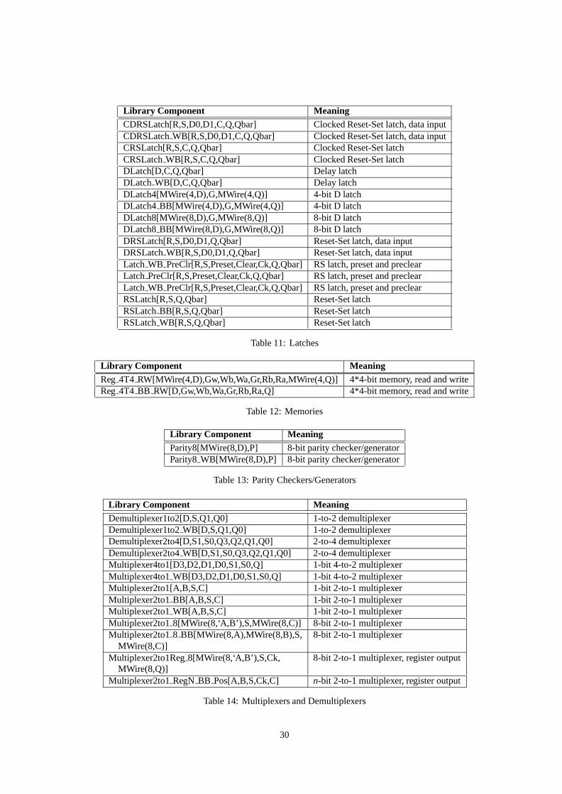
Library Component MeaningCDRSLatch[R,S,D0,D1,C,Q,Qbar] ClockedReset-Setlatch,datainputCDRSLatchWB[R,S,D0,D1,C,Q,Qbar] ClockedReset-Setlatch,datainputCRSLatch[R,S,C,Q,Qbar] ClockedReset-SetlatchCRSLatchWB[R,S,C,Q,Qbar] ClockedReset-SetlatchDLatch[D,C,Q,Qbar] DelaylatchDLatch WB[D,C,Q,Qbar] DelaylatchDLatch4[MWire(4,D),G,MWire(4,Q)] 4-bit D latchDLatch4BB[MWire(4,D),G,MWire(4,Q)] 4-bit D latchDLatch8[MWire(8,D),G,MWire(8,Q)] 8-bit D latchDLatch8BB[MWire(8,D),G,MWire(8,Q)] 8-bit D latchDRSLatch[R,S,D0,D1,Q,Qbar] Reset-Setlatch,datainputDRSLatchWB[R,S,D0,D1,Q,Qbar] Reset-Setlatch,datainputLatch WB PreClr[R,S,Preset,Clear,Ck,Q,Qbar] RSlatch,presetandpreclearLatch PreClr[R,S,Preset,Clear,Ck,Q,Qbar] RSlatch,presetandpreclearLatch WB PreClr[R,S,Preset,Clear,Ck,Q,Qbar] RSlatch,presetandpreclearRSLatch[R,S,Q,Qbar] Reset-SetlatchRSLatchBB[R,S,Q,Qbar] Reset-SetlatchRSLatchWB[R,S,Q,Qbar] Reset-Setlatch
Table11: Latches
Library Component MeaningReg 4T4 RW[MWire(4,D),Gw,Wb,Wa,Gr,Rb,Ra,MWire(4,Q)] 4*4-bit memory, readandwriteReg 4T4 BB RW[D,Gw,Wb,Wa,Gr,Rb,Ra,Q] 4*4-bit memory, readandwrite
Table12: Memories
Library Component MeaningParity8[MWire(8,D),P] 8-bit paritychecker/generatorParity8 WB[MWire(8,D),P] 8-bit paritychecker/generator
Table13: Parity Checkers/Generators
Library Component MeaningDemultiplexer1to2[D,S,Q1,Q0] 1-to-2demultiplexerDemultiplexer1to2WB[D,S,Q1,Q0] 1-to-2demultiplexerDemultiplexer2to4[D,S1,S0,Q3,Q2,Q1,Q0] 2-to-4demultiplexerDemultiplexer2to4WB[D,S1,S0,Q3,Q2,Q1,Q0] 2-to-4demultiplexerMultiplexer4to1[D3,D2,D1,D0,S1,S0,Q] 1-bit 4-to-2multiplexerMultiplexer4to1WB[D3,D2,D1,D0,S1,S0,Q] 1-bit 4-to-2multiplexerMultiplexer2to1[A,B,S,C] 1-bit 2-to-1multiplexerMultiplexer2to1BB[A,B,S,C] 1-bit 2-to-1multiplexerMultiplexer2to1WB[A,B,S,C] 1-bit 2-to-1multiplexerMultiplexer2to18[MWire(8,‘A,B’),S,MWire(8,C)] 8-bit 2-to-1multiplexerMultiplexer2to18 BB[MWire(8,A),MWire(8,B),S, 8-bit 2-to-1multiplexer
MWire(8,C)]Multiplexer2to1Reg 8[MWire(8,‘A,B’),S,Ck, 8-bit 2-to-1multiplexer, registeroutput
MWire(8,Q)]Multiplexer2to1RegN BB Pos[A,B,S,Ck,C] n-bit 2-to-1multiplexer, registeroutput
Table14: MultiplexersandDemultiplexers
30

Library Component MeaningBucketBrigade2[J0,J1,K0,C,Q0,Q1] 2-bit bucketbrigadePassOn2[D,C0,C1,Q] 2-bit sequentialpass-onRegister4[MWire(4,D), Clk, MWire(4,Q)] 4-bit D-typeregisterRegister4BB Neg [MWire(4,D), C, MWire(4,Q)] 4-bitD-typeregister, dataoutputon
negativeclockRegister4BB Pos[MWire(4,D), C, MWire(4,Q)] 4-bit D-typeregister,dataoutputon
positiveclockRegister8[MWire(8,D),C,MWire(8,‘Q,Qbar’)] 8-bit registerRegisterN BB Neg[D,C,Q,Qbar] n-bit register, dataoutputon nega-
tiveclockRegisterN BB Pos[D,C,Q,Qbar] n-bit register, dataoutputon posi-
tiveclockRegisterLoadClr[D,G,Clr,Clk,Q] 1-bit register, dataloadenable,pre-
clear,dataoutputonpositiveclockRegisterLoadClr4[MWire(4,D),G,Clr,Clk,MWire(4,Q)] 4-bit register, dataloadenable,pre-
clear, dataoutputonpositiveclockRegisterLoadClr4Tri[M,N,MWire(4,D),G1,G2,Clr,Clk, 4-bit register, dataloadenable,pre-
MWire(4,Q)] clear, tri-stateoutput, data outputonpositiveclock
RegisterLoadClrBB Neg[D,G,Clr,Clk,Q] 1-bit register, dataloadenable,pre-clear,dataoutputonnegative clock
RegisterLoadClrBB Pos[D,G,Clr,Clk,Q] 1-bit register, dataloadenable,pre-clear,dataoutputonpositiveclock
RegisterLoadClr4BB Neg[D,G,Clr,Clk,Q] 4-bit register, dataloadenable,pre-clear,dataoutputonnegative clock
RegisterLoadClr4BB Pos[D,G,Clr,Clk,Q] 4-bit register, dataloadenable,pre-clear,dataoutputonpositiveclock
ShiftRegister2[D,C,Q0,Q1] 2-bit shift registerShiftRegister2BB Neg[D,C,Q1,Q0] 2-bit shift register, dataoutputon
negativeclockShiftRegister2BB Pos[D,C,Q1,Q0] 2-bit shift register, dataoutputon
positiveclockShiftRegister8[D0,C,D8] 8-bit shift registerShiftRegister8BB Neg[D,C,MWire(8,Q)] 8-bit shift register, dataoutputon
negativeclockShiftRegister8BB Pos[D,C,MWire(8,Q)] 8-bit shift register, dataoutputon
positiveclock
Table15: Registers
31

C Gate-Level ComponentSpecifications
This appendixgivesgate-level circuit specificationsfor thenew DILL components.Specificationsfor theoriginalDILL componentscanbefoundin [4].
C.1 8-Bit Ripple Adder
Seefigure12.
processRippleAdder8[MWire(8,‘A,B’),c0, MWire(8,S),c8] :noexithide MWire(7,c+)inMComp(8,c,‘FullAdder[A,B,C,S,C+]’)c0zero[c0]
endproc (* RippleAdder8*)
Figure12: 8-Bit RippleAdder
C.2 3-to-8Line Decoder
Seefigure13.
processDecoder3To8[MWire(3,D),MWire(8,Y)] : noexithide MWire(3,Ind)in
(MComp(3,‘Inverter[D,Ind]’))D2,D1,D0,Ind2,Ind1,Ind0
(And3[D2,D1,D0,Y7] And3[Ind2,Ind1,Ind0,Y0])D2,D1,D0,Ind2,Ind1,Ind0
(And3[D2,D1,Ind0,Y6] And3[Ind2,Ind1,D0,Y1])D2,D1,D0,Ind2,Ind1,Ind0
(And3[D2,Ind1,D0,Y5] And3[Ind2,D1,Ind0,Y2])D2,D1,D0,Ind2,Ind1,Ind0
(And3[D2,Ind1,Ind0,Y4] And3[Ind2,D1,D0,Y3])endproc (* Decoder3To8*)
C.3 BCD-to-DecimalDecoder
Seefigure14. Outputsare0 active.
processBCDtoDec[MWire(4,D),MWire(10,Y)] : noexithide MWire(4,Ind),MWire(10,Ybar)inMComp(4,‘Inverter[D,Ind]’)MWire(4,‘D,Ind’)(
32

Figure13: 3-to-8Line Decoder
33

((((((((Nand4[Ind3,Ind2,Ind1,Ind0,Y0] Ind3,Ind2,Ind1Nand4[Ind3,Ind2,Ind1,D0,Y1]) Ind3,Ind2,Ind0Nand4[Ind3,Ind2,D1,Ind0,Y2]) Ind3,Ind2,D1,D0Nand4[Ind3,Ind2,D1,D0,Y3]) Ind3,Ind1,Ind0Nand4[Ind3,D2,Ind1,Ind0,Y4]) Ind3,D2,Ind1,D0Nand4[Ind3,D2,Ind1,D0,Y5]) Ind3,D2,D1,Ind0Nand4[Ind3,D2,D1,Ind0,Y6]) Ind3,D2,D1,D0Nand4[Ind3,D2,D1,D0,Y7]) Ind2,Ind1,Ind0Nand4[D3,Ind2,Ind1,Ind0,Y8]) D3,Ind2,Ind1,D0Nand4[D3,Ind2,Ind1,D0,Y9]
)endproc (* BCDtoDec*)
Figure14: BCD-to-DecimalDecoder
C.4 Excess-3-toDecimalDecoder
Outputsare0 active.
processExcess3toDec[MWire(4,D),MWire(10,Y)] : noexithide MWire(4,Ind),MWire(10,Ybar)inMComp(4,‘Inverter[D,Ind]’)MWire(4,‘D,Ind’)(
((((((((Nand4[Ind3,Ind2,D1,D0,Y0] Ind3Nand4[Ind3,D2,Ind1,Ind0,Y1]) Ind3,D2,Ind1,Ind0
34
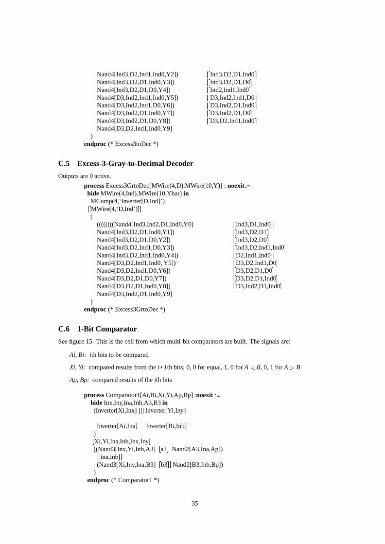
Nand4[Ind3,D2,Ind1,Ind0,Y2]) Ind3,D2,D1,Ind0Nand4[Ind3,D2,D1,Ind0,Y3]) Ind3,D2,D1,D0Nand4[Ind3,D2,D1,D0,Y4]) Ind2,Ind1,Ind0Nand4[D3,Ind2,Ind1,Ind0,Y5]) D3,Ind2,Ind1,D0Nand4[D3,Ind2,Ind1,D0,Y6]) D3,Ind2,D1,Ind0Nand4[D3,Ind2,D1,Ind0,Y7]) D3,Ind2,D1,D0Nand4[D3,Ind2,D1,D0,Y8]) D3,D2,Ind1,Ind0Nand4[D3,D2,Ind1,Ind0,Y9]
)endproc (* Excess3toDec*)
C.5 Excess-3-Gray-to-DecimalDecoder
Outputsare0 active.
processExcess3GrtoDec[MWire(4,D),MWire(10,Y)] : noexithide MWire(4,Ind),MWire(10,Ybar)inMComp(4,‘Inverter[D,Ind]’)MWire(4,‘D,Ind’)(
((((((((Nand4[Ind3,Ind2,D1,Ind0,Y0] Ind3,D1,Ind0Nand4[Ind3,D2,D1,Ind0,Y1]) Ind3,D2,D1Nand4[Ind3,D2,D1,D0,Y2]) Ind3,D2,D0Nand4[Ind3,D2,Ind1,D0,Y3]) Ind3,D2,Ind1,Ind0Nand4[Ind3,D2,Ind1,Ind0,Y4]) D2,Ind1,Ind0Nand4[D3,D2,Ind1,Ind0,Y5]) D3,D2,Ind1,D0Nand4[D3,D2,Ind1,D0,Y6]) D3,D2,D1,D0Nand4[D3,D2,D1,D0,Y7]) D3,D2,D1,Ind0Nand4[D3,D2,D1,Ind0,Y8]) D3,Ind2,D1,Ind0Nand4[D3,Ind2,D1,Ind0,Y9]
)endproc (* Excess3GrtoDec*)
C.6 1-Bit Comparator
Seefigure15. This is thecell from whichmulti-bit comparatorsarebuilt. Thesignalsare:
Ai, Bi: ith bits to becompared
Xi, Yi: comparedresultsfrom the i+1 th bits;0, 0 for equal,1, 0 for A B, 0, 1 for A B
Ap,Bp: comparedresultsof the ith bits
processComparator1[Ai,Bi,Xi,Yi,Ap,Bp] :noexithide Inx,Iny,Ina,Inb,A3,B3in(Inverter[Xi,Inx] Inverter[Yi,Iny]
Inverter[Ai,Ina] Inverter[Bi,Inb])Xi,Yi,Ina,Inb,Inx,Iny((Nand3[Inx,Yi,Inb,A3] a3 Nand2[A3,Ina,Ap])
ina,inb(Nand3[Xi,Iny,Ina,B3] b3 Nand2[B3,Inb,Bp])
)endproc (* Comparator1*)
35

Figure15: 1-Bit Comparator
C.7 4-Bit Comparator
Seefigure16.
processComparator4[Ls4,Gr4,MWire(4,‘X,Y’),Ls0,Gr0] :noexithide MWire(3,‘Ls+,Gr+’) inMComp(4,‘Ls,Gr’,‘Comparator1[Ls+,Gr+,X,Y,Ls,Gr]’)
endproc (* Comparator4*)
Figure16: 4-Bit Comparator
C.8 8-Bit ComparatorprocessComparator8[Ls8,Gr8,MWire(8,‘X,Y’),Ls0,Gr0] :noexithide Ls4,Gr4in(Zero[Ls8] Zero[Gr8])Ls8,Gr8Comparator4[Ls8,Gr8,MWire(4,‘X+++,Y+++’),Ls4,Gr4]
Ls4,Gr4Comparator4[Ls4,Gr4,MWire(4,‘X,Y’),Ls0,Gr0]
endproc (* Comparator8*)
C.9 4-Bit Binary Counter with Reset(74LS93)
Seefigure17.
R1,R2: AsynchronousResetinputs,1 active
Q4: clocksignal
36
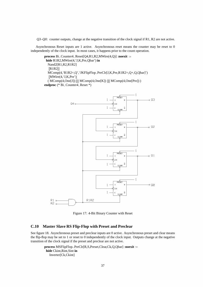
Q3–Q0: counteroutputs,changeat thenegative transitionof theclock signalif R1,R2arenot active.
AsynchronousResetinputs are1 active. Asynchronousresetmeansthe countermay be resetto 0independentlyof theclock input. In mostcases,it happensprior to thecountoperation.
processBi Counter4Reset[Q4,R1,R2,MWire(4,Q)] :noexithide R1R2,MWire(4,‘J,K,Pre,Qbar’)inNand2[R1,R2,R1R2]
R1R2MComp(4,‘R1R2=,Q’,‘JKFlipFlopPreClr[J,K,Pre,R1R2=,Q+,Q,Qbar]’)
MWire(4,‘J,K,Pre’)( MComp(4,One[J]) MComp(4,One[K]) MComp(4,One[Pre]))
endproc (* Bi Counter4Reset*)
Figure17: 4-Bit BinaryCounterwith Reset
C.10 Master SlaveRSFlip-Flop with Presetand Preclear
Seefigure18. Asynchronouspresetandpreclearinputsare0 active. Asynchronouspresetandclearmeanstheflip-flop maybesetto 1 or resetto 0 independentlyof theclock input. Outputschangeat thenegativetransitionof theclock signalif thepresetandprecleararenotactive.
processMSFlipFlop PreClr[R,S,Preset,Clear,Ck,Q,Qbar]:noexithide Ckint,Rint,Sintin
Inverter[Ck,Ckint]
37

Ck,Ckint( CRSLatch[R,S,Ck,Rint,Sint]
Rint,SintLatch PreClr[Sint,Rint,Preset,Clear,Ckint,Q,Qbar]
)endproc (* MSFlipFlop PreClr*)
Figure18: Master-Slave RSFlip-Flopwith PresetandPreclear
C.11 Master SlaveJK Flip-Flop With Presetand Preclear
Asynchronouspresetandpreclearinputsare0 active. Outputschangeatthenegative transitionof theclocksignalif thepresetandprecleararenot active.
processJKFlipFlop PreClr[J,K,Preset,Clear,Ck,Q,Qbar]:noexit
38

hide Rint,Sintin(And2[J,Qbar,Sint] And2[K,Q,Rint])Rint,Sint,Q,QbarMSFlipFlop PreClr[Rint,Sint,Preset,Clear,Ck,Q,Qbar]
endproc (* JKFlipFlop PreClr*)
C.12 Master SlaveD Flip-Flop With Presetand Preclear
Asynchronouspresetandpreclearinputsare0 active. Outputschangeatthenegative transitionof theclocksignalif thepresetandprecleararenot active.
processDFlipFlop PreClr[D,Preset,Clear,Ck,Q,Qbar]:noexithide Dint inInverter[D,Dint]
D,DintJKFlipFlop PreClr[D,Dint,Preset,Clear,Ck,Q,Qbar]
endproc (* DFlipFlop PreClr*)
C.13 Edge-TriggeredRS Flip-Flop
Outputschangeat thenegative transitionof theclocksignal.
processRSFlipFlopEdge[R,S,Ck,Q,Qbar]: noexithide A,B,C,D in((Nand2[S,Ck,A] A,Ck Or2[Ck,A,C]) C Nand2[C,Qbar,Q])Ck,Q,Qbar((Nand2[R,Ck,B] B,Ck Or2[Ck,B,D]) D Nand2[D,Q,Qbar])
endproc (* RSFlipFlopEdge*)
C.14 RSLatch with Presetand Preclear
Seefigure19. Asynchronouspresetandpreclearare0 active. OutputschangewhenCK is 1 if thepresetandprecleararenot active.
processLatch PreClr[R,S,Preset,Clear,Ck,Q,Qbar]:noexithide Rint,Sintin(Nand3[S,Clear,Ck,Sint] Ck Nand3[R,Preset,Ck,Rint])Rint,Sint,Preset,Clear(Nand3[Sint,Preset,Qbar,Q] Q,Qbar Nand3[Rint,Clear,Q,Qbar])
endproc (* Latch PreClr*)
Figure19: RSLatchwith PresetandPreclear
39
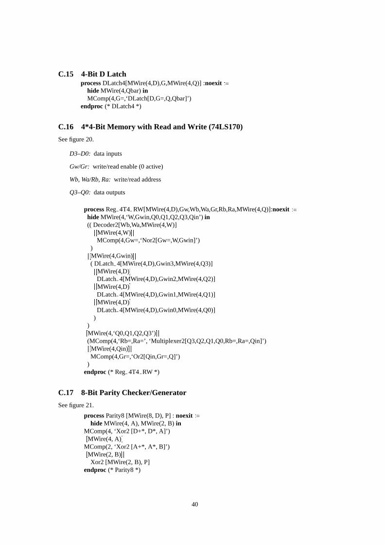
C.15 4-Bit D LatchprocessDLatch4[MWire(4,D),G,MWire(4,Q)] :noexit
hide MWire(4,Qbar)inMComp(4,G=,‘DLatch[D,G=,Q,Qbar]’)
endproc (* DLatch4*)
C.16 4*4-Bit Memory with Readand Write (74LS170)
Seefigure20.
D3–D0: datainputs
Gw/Gr: write/readenable(0 active)
Wb,Wa/Rb,Ra: write/readaddress
Q3–Q0: dataoutputs
processReg 4T4 RW[MWire(4,D),Gw,Wb,Wa,Gr,Rb,Ra,MWire(4,Q)]:noexithide MWire(4,‘W,Gwin,Q0,Q1,Q2,Q3,Qin’)in(( Decoder2[Wb,Wa,MWire(4,W)]
MWire(4,W)MComp(4,Gw=,‘Nor2[Gw=,W,Gwin]’)
)MWire(4,Gwin)( DLatch 4[MWire(4,D),Gwin3,MWire(4,Q3)]
MWire(4,D)DLatch 4[MWire(4,D),Gwin2,MWire(4,Q2)]MWire(4,D)DLatch 4[MWire(4,D),Gwin1,MWire(4,Q1)]MWire(4,D)DLatch 4[MWire(4,D),Gwin0,MWire(4,Q0)]
))MWire(4,‘Q0,Q1,Q2,Q3’)(MComp(4,‘Rb=,Ra=’,‘Multiplexer2[Q3,Q2,Q1,Q0,Rb=,Ra=,Qin]’)
MWire(4,Qin)MComp(4,Gr=,‘Or2[Qin,Gr=,Q]’)
)endproc (* Reg 4T4 RW *)
C.17 8-Bit Parity Checker/Generator
Seefigure21.
processParity8 [MWire(8,D), P] : noexithide MWire(4,A), MWire(2,B) in
MComp(4,‘Xor2 [D+*, D*, A]’)MWire(4,A)
MComp(2,‘Xor2 [A+*, A*, B]’)MWire(2,B)Xor2 [MWire(2,B), P]
endproc (* Parity8 *)
40

Figure20: 4*4-Bit Memorywith ReadandWrite
41

Figure21: 8-Bit Parity Checker/Generator
C.18 2-1Multiplexer
Seefigure22.
processMultiplexer2to1[A,B,S,C]:noexithide Ain,BIn,Sin in(Inverter[S,Sin]S,Sin( And2[A,Sin,Ain] And2[B,S,BIn]))Ain,BInOr2[Ain,BIn,C]
endproc (* Multiplexer2to1*)
Figure22: 2-to-1Multiplexer
C.19 8-bit 2-1MultiplexerprocessMultiplexer2to1 8[MWire(8,‘A,B’),S,MWire(8,C)] :noexit
MComp(8,S=,‘Multiplexer2to1[A,B,S=,C]’)endproc (* Multiplexer2to1 8 *)
C.20 8-bit 2-1Multiplexer with RegisterOutput
Outputschangeat thenegative transitionof theclocksignal.
processMultiplexer2to1Reg 8[MWire(8,‘A,B’),S,Ck,MWire(8,Q)] :noexithide MWire(8,‘C,Qbar’)in
42
Multiplexer2to1 8[MWire(8,‘A,B’),S,MWire(8,C)]MWire(8,C)Multiplexer 8[MWire(8,C),Ck,MWire(8,‘Q,Qbar’)]
endproc (* Multiplexer2to1Reg 8 Decl *)
C.21 8-Bit Register
D7–D0: datainputs
Q7–Q0: dataoutputs
Qbar7–Qbar0:dataoutputsnegated
C: commonclock input
Outputschangeat thenegative transitionof theclock signal.
processRegister 8 [MWire(8,D), C,MWire(8,‘Q,Qbar’)]: noexitMComp(8,C=, ‘DFlipFlop[D, C=,Q, Qbar]’)
endproc (* Register 8 *)
C.22 8-Bit Shift Register
D8: datainput
D0: dataoutput
C: commonclock input
Dataoutputchangesat thenegative transitionof theclocksignal.
processShiftRegister8[D0, C,D8] : noexithide MWire(7,D+),
MWire(8,Dbar+)inMComp(8,‘D, C=’, ‘DFlipFlop[D, C=, D+, Dbar+]’)
MWire(8,Dbar+)MComp(8,‘Sink [Dbar+]’)
endproc (* ShiftRegister8*)
C.23 4-Bit D-TypeRegisterwith Tri-State Output (74LS173)
Seefigure23.
D3–D0: datainputs
G1,G2: dataenable,usedto selectregister(0 active)
Clr: asynchronousclear
Clk: clock
M, N: outputcontrol
Q3–Q0: dataoutputs
Dataoutputschangeat thepositivetransitionof theclock signal.
43
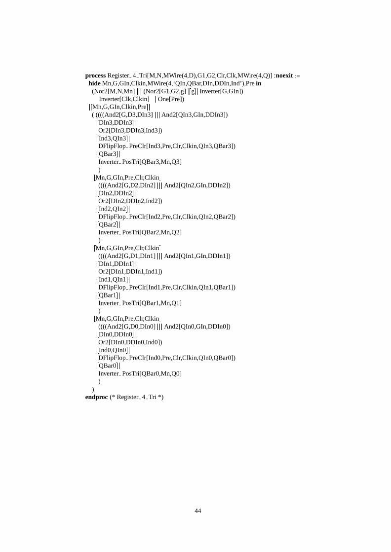
processRegister 4 Tri[M,N,MWire(4,D),G1,G2,Clr,Clk,MWire(4,Q)] :noexithide Mn,G,GIn,Clkin,MWire(4,‘QIn,QBar,DIn,DDIn,Ind’),Prein(Nor2[M,N,Mn] (Nor2[G1,G2,g] g Inverter[G,GIn])
Inverter[Clk,Clkin] One[Pre])Mn,G,GIn,Clkin,Pre( ((((And2[G,D3,DIn3] And2[QIn3,GIn,DDIn3])
DIn3,DDIn3Or2[DIn3,DDIn3,Ind3])Ind3,QIn3DFlipFlop PreClr[Ind3,Pre,Clr,Clkin,QIn3,QBar3])QBar3Inverter PosTri[QBar3,Mn,Q3])
Mn,G,GIn,Pre,Clr,Clkin((((And2[G,D2,DIn2] And2[QIn2,GIn,DDIn2])DIn2,DDIn2Or2[DIn2,DDIn2,Ind2])Ind2,QIn2DFlipFlop PreClr[Ind2,Pre,Clr,Clkin,QIn2,QBar2])QBar2Inverter PosTri[QBar2,Mn,Q2])
Mn,G,GIn,Pre,Clr,Clkin((((And2[G,D1,DIn1] And2[QIn1,GIn,DDIn1])DIn1,DDIn1Or2[DIn1,DDIn1,Ind1])Ind1,QIn1DFlipFlop PreClr[Ind1,Pre,Clr,Clkin,QIn1,QBar1])QBar1Inverter PosTri[QBar1,Mn,Q1])
Mn,G,GIn,Pre,Clr,Clkin((((And2[G,D0,DIn0] And2[QIn0,GIn,DDIn0])DIn0,DDIn0Or2[DIn0,DDIn0,Ind0])Ind0,QIn0DFlipFlop PreClr[Ind0,Pre,Clr,Clkin,QIn0,QBar0])QBar0Inverter PosTri[QBar0,Mn,Q0])
)endproc (* Register 4 Tri *)
44

Figure23: 4-Bit D-TypeRegisterwith Tri-StateOutput
45

D Signalsin the Sub-CPU
D.1 Signalsin the Behaviour Specification
LOTOS gatesin thebehaviour specificationof thesub-CPUmayrepresenteithermulti-bit wiresor one-bitwires.
IR: Instructioninput,9-bit wire
DtIn: DataInput from thememory, 4-bit wire
Clk: systemClock,one-bitwire
R3,R2,R1,R0:outputsof four dataRegisters,eachoutputbeinga 4-bit wire; shortenedasMWire(4,R)
Flag1,Flag0: outputsof flag registers,eacha 1-bit wire; Flag1is thecarryflag andFlag0thecomparisonflag,with 1 meaningtwo operandsareequaland0 thatthey areunequal
BusAorMArr: MemoryAddress,4-bit wire
BusBorDtOut: DataOutputto memory, 4-bit wire
MW: MemoryWrite signal.one-bitwire. 1 standsfor memorywrite enable,0 for memorywrite disable
D.2 Signalsin the Structural Specification
LOTOS gatesin thestructuralspecificationrepresentone-bitwires. Multi-bit wirescanbeshortenedwithMWire macro.
MWire(9,IR): Instructioninputs
MWire(4,DtIn): DataInputsfrom thememory
Clk: sameasthatin thebehaviour specification
MWire(4,‘R3,R2,R1,R0’): the outputsof the four data Registers; for example, R33 is the mostsignificantbit of theregisterR3
Flag1,Flag0: sameasthatin thebehaviour specification
MWire(4,‘BusAorMArr’): theinternalBusfor sourceoperandA within thesub-CPU,or theexternalbusfor MemoryAddress
MWire(4,‘BusBorDtOut’): theinternalBusfor sourceoperandB within thesub-CPU,or theexternalbusfor DataOutputsto memory
MW: sameasthatin thebehaviour specification
Thefollowing aretheimportantcontrolsignalsfrom thecontrolunit of thesub-CPU:
RW: RegisterWrite signal;1 standsfor write enable,0 for disable
AorC: Addition or Comparison;1 standsfor addition,0 for comparison
MorF: datacomesfrom Memoryor from functionunit (ALU); 1 standsfor from memory, 0 for fromfunctionunit
LI: dataloadedfrom immediateoperandor from amemoryunit; 1 standsfor loadingfrom immediateoperand,0 for from a memoryunit
ADD: 1 standsfor anadditioninstruction
46

CMP: 1 standsfor a comparisoninstruction
MWire(4,G): determinethedestinationregister, 1 active; for example0001meansthattheloadeddatawill besentto registerR0.
MWire(4,SA):determinethevalueontheBusAbus,1 active; for example0001meansthatthecontentof registerR0will beappearonBusA, thesignalscontrollingtheenablepinsof thetri-stategates
MWire(4,SB):similar to MWire(4,SA)but referringto theBusBbus
47
E Behaviour Specificationof the Sub-CPU
This is a simplified behaviour specificationof the sub-CPU.In the specification,we assumethat if aninstructionneedsto geta valuefrom registersor databuses,but thevalueis anarbitraryoneat that time,this instructionwill beneglected.
Theassumptionmakesthebehaviour specificationmoreconcisethanacompleteoneand,moreimpor-tantly, makesthesimulationvery easydueto theomissionof settingthesearbitraryvaluesexplicitly. Ontheotherhand,acompletespecificationis moreprecisethanthisone.It wouldspecifyall theoutputstatesof thesub-CPU,includingthosecorrespondingto theinitial undeterminedinputs.
divert( 1)include(dill.m4)divert
define(cpu gates,‘IR,DtIn,Clk,MWire(4,R),Flag1,Flag0,BusAorMArr,BusBorDtOut,MW’)
define(cpu pars,‘dtIR,dtDtIn,dtClk,MWire(4,dtR), dtFlag1,dtFlag0,dtBusAorMArr,dtBusBorDtOut,dtMW’)
circuit(‘cpu beha[cpugates]’,‘cpu beha[cpugates]
where
processcpu beha[cpugates]: noexitcpu behaAux[cpugates]
(bit(X)#X#X#X#X#X#X#X#X,bit(X)#X#X#X,X of bit,bit(X)#X#X#X,bit(X)#X#X#X,bit(X)#X#X#X,bit(X)#X#X#X,X of bit, X of bit,bit(X)#X#X#X,bit(X)#X#X#X,X of bit)
whereprocesscpu behaAux[cpugates]
(dtIR,dtDtIn: BitArray,dtClk: Bit,MWire(4,dtR):BitArray,dtFlag1,dtFlag0: Bit,dtBusAorMArr,dtBusBorDtOut:BitArray,dtMW: Bit) : noexit
IR ? dtIR: BitArray;cpu behaAux[cpugates](cpupars)
DtIn ? dtDtIn: BitArray;cpu behaAux[cpugates](cpupars)
Clk ? newdtClk: Bit;([(dtClk ne0 of bit) or (newdtClk ne1 of bit) or (dtIR eqbit(x))]
cpu behaAux[cpugates](Pars(dtClk,‘cpupars’))
48

[(dtClk eq0 of bit) and(newdtClk eq1 of bit) and(dtIR nebit(x))](
[(dtIR.natnum(7)eq0 of bit) and(dtIR.natnum(6)eq1 of bit)] (* store*)(cpu behaAux[cpugates](Pars(dtClk,‘cpu pars’))
) (* endof store*)
[(dtIR.natnum(7)eq1 of bit) and(dtIR.natnum(6)eq0 of bit)] (* load*)([(dtDtIn eqbit(x)) and(dtIR.natnum(8)eq0 of bit) ]cpu behaAux[cpugates](Pars(dtClk,‘cpu pars’))
[dtDtIn nebit(x) or (dtIR.natnum(8)eq1 of bit) ]( let newreg: BitArray =
bittoba(dtIR.natnum(3),dtIR.natnum(2),dtIR.succ(0),dtIR.0) in([(dtIR.natnum(5)eq0 of bit) and(dtIR.natnum(4)eq0 of bit)]([(dtR0nedtDtIn) and(dtIR.natnum(8)eq0 of bit)]R0 ! dtDtIn;( let dtR0: BitArray = dtDtIn incpu behaAux[cpugates](Pars(dtClk,‘cpu pars’)))
[(dtR0eqdtDtIn) and(dtIR.natnum(8)eq0 of bit)]cpu behaAux[cpugates](Pars(dtClk,‘cpu pars’))
[(dtIR.natnum(8)eq1 of bit) and(dtR0nenewreg)]R0! newreg;( let dtR0: BitArray = newreg incpu behaAux[cpugates](Pars(dtClk,‘cpupars’))
)
[(dtIR.natnum(8)eq1 of bit) and(dtR0eqnewreg)]cpu behaAux[cpugates](Pars(dtClk,‘cpu pars’))
)
[(dtIR.natnum(5)eq0 of bit) and(dtIR.natnum(4)eq1 of bit)]([(dtR1nedtDtIn) and(dtIR.natnum(8)eq0 of bit)]R1 ! dtDtIn;( let dtR1: BitArray = dtDtIn incpu behaAux[cpugates](Pars(dtClk,‘cpu pars’))
)
[(dtR1eqdtDtIn) and(dtIR.natnum(8)eq0 of bit)]cpu behaAux[cpugates](Pars(dtClk,‘cpu pars’))
[(dtIR.natnum(8)eq1 of bit) and(dtR1nenewreg)]R1! newreg;( let dtR1: BitArray = newreg incpu behaAux[cpugates](Pars(dtClk,‘cpupars’))
)
49

[(dtIR.natnum(8)eq1 of bit) and(dtR1eqnewreg)]cpu behaAux[cpugates](Pars(dtClk,‘cpu pars’))
)
[(dtIR.natnum(5)eq1 of bit) and(dtIR.natnum(4)eq0 of bit)]([(dtIR.natnum(8)eq0 of bit) and(dtR2nedtDtIn)]R2 ! dtDtIn;( let dtR2: BitArray = dtDtIn incpu behaAux[cpugates](Pars(dtClk,‘cpu pars’)))
[(dtIR.natnum(8)eq0 of bit) and(dtR2eqdtDtIn)]cpu behaAux[cpugates](Pars(dtClk,‘cpu pars’))
[(dtIR.natnum(8)eq1 of bit) and(dtR2nenewreg)]R2! newreg;( let dtR2: BitArray = newreg incpu behaAux[cpugates](Pars(dtClk,‘cpu pars’)))
[(dtIR.natnum(8)eq1 of bit) and(dtR2eqnewreg)]cpu behaAux[cpugates](Pars(dtClk,‘cpu pars’))
)
[(dtIR.natnum(5)eq1 of bit) and(dtIR.natnum(4)eq1 of bit)]([(dtIR.natnum(8)eq0 of bit) and(dtR3nedtDtIn)]R3 ! dtDtIn;( let dtR3: BitArray = dtDtIn incpu behaAux[cpugates](Pars(dtClk,‘cpu pars’)))
[(dtIR.natnum(8)eq0 of bit) and(dtR3eqdtDtIn)]cpu behaAux[cpugates](Pars(dtClk,‘cpu pars’))
[(dtIR.natnum(8)eq1 of bit) and(dtR3nenewreg)]R3! newreg;( let dtR3: BitArray = newreg incpu behaAux[cpugates](Pars(dtClk,‘cpu pars’)))
[(dtIR.natnum(8)eq1 of bit) and(dtR3eqnewreg)]cpu behaAux[cpugates](Pars(dtClk,‘cpu pars’))
)) (* endof let *)
) (* endof dtDtIn nebit(x) *)) (* endof load*)
[((dtIR.natnum(7)eq0 of bit) and(dtIR.natnum(6)eq0 of bit)) or((dtIR.natnum(7)eq1 of bit) and(dtIR.natnum(6)eq1 of bit)) ]((
50

([(dtIR.succ(0)eq0 of bit) and(dtIR.0eq0 of bit)]exit(any BitArray, dtR0)
[(dtIR.succ(0)eq0 of bit) and(dtIR.0eq1 of bit)]exit(any BitArray, dtR1)
[(dtIR.succ(0)eq1 of bit) and(dtIR.0eq0 of bit)]exit(any BitArray, dtR2)
[(dtIR.succ(0)eq1 of bit) and(dtIR.0eq1 of bit)]exit(any BitArray, dtR3)
)
([(dtIR.natnum(3)eq0 of bit) and(dtIR.natnum(2)eq0 of bit)]exit(dtR0,any BitArray)
[(dtIR.natnum(3)eq0 of bit) and(dtIR.natnum(2)eq1 of bit)]exit(dtR1,any BitArray)
[(dtIR.natnum(3)eq1 of bit) and(dtIR.natnum(2)eq0 of bit)]exit(dtR2,any BitArray)
[(dtIR.natnum(3)eq1 of bit) and(dtIR.natnum(2)eq1 of bit)]exit(dtR3,any BitArray)
)) (* endof interleaving *)
acceptdtBusAorMArr, dtBusBorDtOut: BitArray in([(dtBusAorMArr eqbit(x)) or ( dtBusBorDtOuteqbit(x))]cpu behaAux[cpugates](Pars(dtClk,‘cpu pars’))
[(dtBusAorMArr nebit(x)) and(dtBusBorDtOutnebit(x))]([(dtIR.natnum(7)eq0 of bit) and(dtIR.natnum(6)eq0 of bit)] (* cmp*)([dtBusAorMArr eqdtBusBorDtOut]([dtFlag0ne1 of bit]Flag0! 1 of bit;( let dtFlag0: Bit = 1 of bit in
cpu behaAux[cpugates](Pars(dtClk,‘cpupars’)))
[dtFlag0eq1 of bit]cpu behaAux[cpugates](Pars(dtClk,‘cpu pars’))
)
[dtBusAorMArr nedtBusBorDtOut]([dtFlag0ne0 of bit]
Flag0! 0 of bit;( let dtFlag0: Bit = 0 of bit incpu behaAux[cpugates](Pars(dtClk,‘cpupars’))
)
[dtFlag0eq0 of bit]
51

cpu behaAux[cpugates](Pars(dtClk,‘cpu pars’)))
) (* endof cmp*)
[(dtIR.natnum(Dec(7))eq1 of bit) and(dtIR.natnum(6)eq1 of bit)] (* add*)( let newdtDr : BitArray = dtBusAorMArr+ dtBusBorDtOut,
newdtCarry: Bit = carry(dtBusAorMarr,dtBusBorDtOut) in(([(dtIR.natnum(5)eq0 of bit) and(dtIR.natnum(4)eq0 of bit)]([dtR0nenewdtDr]R0 ! newdtDr;exit( dtR3,dtR2,dtR1,newdtDr, any bit)
[dtR0eqnewdtDr ]exit( dtR3,dtR2,dtR1,newdtDr, any bit)
)
[(dtIR.natnum(5)eq0 of bit) and(dtIR.natnum(4)eq1 of bit)]([dtR1nenewdtDr]R1 ! newdtDr;exit( dtR3,dtR2,newdtDr,dtR0,any bit)
[dtR1eqnewdtDr]exit( dtR3,dtR2,newdtDr,dtR0,any bit))
[(dtIR.natnum(5)eq1 of bit) and(dtIR.natnum(4)eq0 of bit)](
[dtR2nenewdtDr]R2 ! newdtDr;exit( dtR3,newdtDr,dtR1,dtR0,any bit)
[dtR2eqnewdtDr]exit( dtR3,newdtDr,dtR1,dtR0,any bit)
)
[(dtIR.natnum(5)eq1 of bit) and(dtIR.natnum(4)eq1 of bit)]([dtR3nenewdtDr]R3 ! newdtDr;exit( newdtDr,dtR2,dtR1,dtR0,any bit)
[dtR3eqnewdtDr]exit( newdtDr,dtR2,dtR1,dtR0,any bit)
)) (* endof registerchanging*)
([dtFlag1nenewdtCarry]Flag1! newdtCarry;
52
exit(MWire(4,any BitArray=),newdtCarry)
[dtFlag1eqnewdtCarry]exit(MWire(4,any BitArray=),newdtCarry)
) (* endof flag1changing*)) (* endof let *)
acceptMWire(4,dtR): BitArray, dtFlag1: Bit incpu behaAux[cpugates](Pars(dtClk,‘cpu pars’))
) (* endof add*)) (* endof sourceAandsourceBnebit(x) *)
) (* endof acceptof BusAandBusB*)) (* endof addor cmp*)
) (* endof appropriatetransition*)) (* endof Clk *)
[(((dtIR.natnum(7)eq0 of bit) and(dtIR.natnum(6)eq0 of bit)) or((dtIR.natnum(7)eq1 of bit) and(dtIR.natnum(6)eq0 of bit)) or((dtIR.natnum(7)eq1 of bit) and(dtIR.natnum(6)eq1 of bit))) and(dtMW ne0 of bit)]MW ! 0 of bit;(let dtMW : bit = 0 of bit incpu behaAux[cpugates](cpupars))
[(dtIR.natnum(Dec(7))eq0 of bit) and(dtIR.natnum(6)eq1 of bit)and(dtMW ne1 of bit) ] (*store*)
MW ! 1 of bit;( let dtMW : Bit = 1 of bit incpu behaAux[cpugates](cpupars))
[(dtIR.natnum(3)eq0 of bit) and(dtIR.natnum(2)eq0 of bit) and(dtR0nedtBusAorMArr)and(dtR0nebit(X)) ]
BusAorMArr ! dtR0;( let dtBusAorMArr : BitArray = dtR0 in
cpu behaAux[cpugates](cpupars))
[(dtIR.natnum(3)eq0 of bit) and(dtIR.natnum(2)eq1 of bit) and(dtR1nedtBusAorMArr)and(dtR1nebit(X))]
BusAorMArr ! dtR1;(let dtBusAorMArr : BitArray = dtR1 incpu behaAux[cpugates](cpupars)
)
[(dtIR.natnum(3)eq1 of bit) and(dtIR.natnum(2)eq0 of bit) and(dtR2nedtBusAorMArr)and(dtR2nebit(X))]
BusAorMArr ! dtR2;(let dtBusAorMArr : BitArray = dtR2 incpu behaAux[cpugates](cpupars)
)
[(dtIR.natnum(3)eq1 of bit) and(dtIR.natnum(2)eq1 of bit) and
53

(dtR3nedtBusAorMArr)and(dtR3nebit(X))]BusAorMArr ! dtR3;(let dtBusAorMArr : BitArray = dtR3 in
cpu behaAux[cpugates](cpupars))
[(dtIR.succ(0)eq0 of bit) and(dtIR.0eq0 of bit) and(dtR0nedtBusBorDtOut)and(dtR0nebit(X))]BusBorDtOut! dtR0;(let dtBusBorDtOut: BitArray = dtR0 incpu behaAux[cpugates](cpupars)
)
[(dtIR.succ(0)eq0 of bit) and(dtIR.0eq1 of bit) and(dtR1nedtBusBorDtOut)and(dtR1nebit(X))]BusBorDtOut! dtR1;(let dtBusBorDtOut: BitArray = dtR1 incpu behaAux[cpugates](cpupars)
)
[(dtIR.succ(0)eq1 of bit) and(dtIR.0eq0 of bit) and(dtR2nedtBusBorDtOut)and(dtR2nebit(X))]BusBorDtOut! dtR2;(let dtBusBorDtOut: BitArray = dtR2 in
cpu behaAux[cpugates](cpupars))
[(dtIR.succ(0)eq1 of bit) and(dtIR.0eq1 of bit) and(dtR3nedtBusBorDtOut)and(dtR3nebit(X))]BusBorDtOut! dtR3;(let dtBusBorDtOut: BitArray = dtR3 incpu behaAux[cpugates](cpupars)
)endproc (* cpu behaAux*)
endproc (* cpu beha*)’)
54

F Structural Specificationof the Sub-CPUdivert( 1)include(dill.m4)divert
define(cpu gates,‘MWire(9,IR),MWire(4,DtIn),Clk,MWire(4,‘R3,R2,R1,R0’),Flag1,Flag0,MWire(4,‘BusAorMArr,BusBorDtOut’),MW’)
circuit(‘cpu abst[cpugates]’,‘hide RW,AorL,MorF,LI,Ls0,ADD,CMP, Gr0,Ls4,Gr4,Carry, Zero,C0,Clr,
MWire(4,Sum),MWire(4,G),MWire(4, ‘Dr,SA,SB’),MWire(4,‘AddA,AddB,ComA,ComB’),MWire(4,Data),MWire(4,RegIn) in
(CtrlWord WB[IR8,IR7,IR6,RW, AorL,MW, MorF, LI, ADD, CMP]
Decoder2WB One[IR5,IR4,MWire(4,Dr)]
Decoder2WB One[IR3,IR2,MWire(4,SA)]
Decoder2WB One[IR1,IR0,MWire(4,SB)])
RW,AorL,MorF,LI,ADD,CMP,MWire(4,‘Dr,SA,SB’), IR3,IR2,IR1,IR0((One[Clr]
Clr( (RegLoadClr4 BB Pos[MWire(4,RegIn),G3,Clr,Clk,MWire(4,R3)] G3 And2[ RW,Dr3,G3])
MWire(4,RegIn),Clk,RW,Clr(RegLoadClr4 BB Pos[MWire(4,RegIn),G2,Clr,Clk,MWire(4,R2)] G2 And2[ RW,Dr2,G2])MWire(4,RegIn),Clk,RW,Clr(RegLoadClr4 BB Pos[MWire(4,RegIn),G1,Clr,Clk,MWire(4,R1)] G1 And2[ RW,Dr1,G1])MWire(4,RegIn),Clk,RW,Clr(RegLoadClr4 BB Pos[MWire(4,RegIn),G0,Clr,Clk,MWire(4,R0)] G0 And2[ RW,Dr0,G0])
))MWire(4,R3),MWire(4,R2),MWire(4,R1),MWire(4,R0),MWire(4,RegIn),Clk,Clr(((
RepeaterOne 4[MWire(4,R3),SA3,MWire(4,BusAorMArr)]MWire(4,BusAorMArr)RepeaterOne 4[MWire(4,R2),SA2,MWire(4,BusAorMArr)]MWire(4,BusAorMArr)RepeaterOne 4[MWire(4,R1),SA1,MWire(4,BusAorMArr)]MWire(4,BusAorMArr)RepeaterOne 4[MWire(4,R0),SA0,MWire(4,BusAorMArr)]
)MWire(4,R3),MWire(4,R2),MWire(4,R1),MWire(4,R0)(RepeaterOne 4[MWire(4,R3),SB3,MWire(4,BusBorDtOut)]MWire(4,BusBorDtOut)RepeaterOne 4[MWire(4,R2),SB2,MWire(4,BusBorDtOut)]MWire(4,BusBorDtOut)
55

RepeaterOne 4[MWire(4,R1),SB1,MWire(4,BusBorDtOut)]MWire(4,BusBorDtOut)RepeaterOne 4[MWire(4,R0),SB0,MWire(4,BusBorDtOut)]
))MWire(4,BusAorMArr),MWire(4,BusBorDtOut)
(((MComp(4,AorL=, ‘Demultiplexer1to2,WB[BusAorMArr,AorL=,AddA,ComA]’)AorLMComp(4,AorL=, ‘Demultiplexer1to2,WB[BusBorDtOut,AorL=,AddB,ComB]’)
)MWire(4,‘AddA,ComA,AddB,ComB’)
(((Zero[C0] C0 Adder4 BB[MWire(4,AddA),MWire(4,AddB),C0,MWire(4,Sum),Carry])
((Zero[Ls4] Zero[Gr4])Ls4,Gr4Comparator4BB[Ls4,Gr4,MWire(4,‘ComA,ComB’),Ls0,Gr0]
Ls0,Gr0Or2[Ls0,Gr0,Zero]))Carry,Zero,MWire(4,Sum)
((
RegLoadClr BB Pos[Carry,ADD,Clr,Clk,Flag1]Clk,Clr
RegLoadClr BB Pos[Zero,CMP,Clr,Clk,Flag0])
(MComp(4,MorF=,‘Mul2to1WB[Sum,DtIn, MorF=,Data]’)MWire(4,Data)MComp(4,LI=,‘Multiplexer2to1 WB[Data,IR,LI=,RegIn]’)
))
))
))
)
where
Decoder2WB One DeclRegLoadClr4 BB Pos DeclRepeaterOne 4 DeclDemultiplexer1to2 WB DeclZero DeclOne DeclOr2 DeclAdder4 BB DeclComparator4BB DeclAnd2 Decl
56

DFlipFlop BB Pos DeclMultiplexer2to1 WB Decl
define(ctrlword,‘IR8,IR7,IR6,RW,AorL,MW,MorF,LI,ADD,CMP’)define(ctrlpars,‘dtIR8,dtIR7,dtIR6,dtRW,dtAorL,dtMW,dtMorF,dtLI,dtADD,dtCMP’)
processCtrlWord WB[ctrlword] : noexitCtrlWord WB Aux[ctrlword](MWire(10,X of bit=))
where
processCtrlWord WB Aux[ctrlword](dtIR8,dtIR7,dtIR6,dtRW,dtAorL,dtMW,dtMorF,dtLI,dtADD,dtCMP:Bit) : noexitIR8 ? dtIR8 : Bit;CtrlWord WB Aux[IR8,IR7,IR6,RW,AorL,MW,MorF,LI,ADD,CMP](ctrlpars)
IR7 ? dtIR7 : Bit;CtrlWord WB Aux[ctrlword](ctrlpars)
IR6 ? dtIR6 : Bit;CtrlWord WB Aux[ctrlword](ctrlpars)
(let newdtRW : Bit = dtIR7,newdtAorL: Bit = dtIR6,newdtLI : Bit = dtIR8and(dtIR7andnot(dtIR6)),newdtMW : Bit = not(dtIR7)anddtIR6,newdtMorF:Bit = (dtIR7xor dtIR6)xor (not(dtIR7)anddtIR6),newdtADD : Bit = dtIR7anddtIR6,newdtCMP: Bit = not(dtIR7)andnot(dtIR6)in
([(newdtRW neX of bit) and(newdtRW nedtRW)]RW ! newdtRW;CtrlWord WB Aux[ctrlword](Pars(dtRW,‘ctrlpars’))
[(newdtAorL neX of bit) and(newdtAorL nedtAorL)]AorL ! newdtAorL;CtrlWord WB Aux[ctrlword](Pars(dtAorL,‘ctrlpars’))
[(newdtMW neX of bit) and(newdtMW nedtMW)]MW ! newdtMW;CtrlWord WB Aux[ctrlword](Pars(dtMW,‘ctrlpars’))
[(newdtMorFneX of bit) and(newdtMorFnedtMorF)]MorF ! newdtMorF;CtrlWord WB Aux[ctrlword](Pars(dtMorF,‘ctrlpars’))
[(newdtLI neX of bit) and(newdtLI nedtLI)]LI ! newdtLI;
CtrlWord WB Aux[ctrlword](Pars(dtLI,‘ctrlpars’))
[(newdtADD neX of bit) and(newdtADD nedtADD)]ADD ! newdtADD;
CtrlWord WB Aux[ctrlword](Pars(dtADD,‘ctrlpars’))
57

[(newdtCMPneX of bit) and(newdtCMPnedtCMP)]CMP! newdtCMP;CtrlWord WB Aux[ctrlword](Pars(dtCMP,‘ctrlpars’))
))
endprocendproc
’)
58
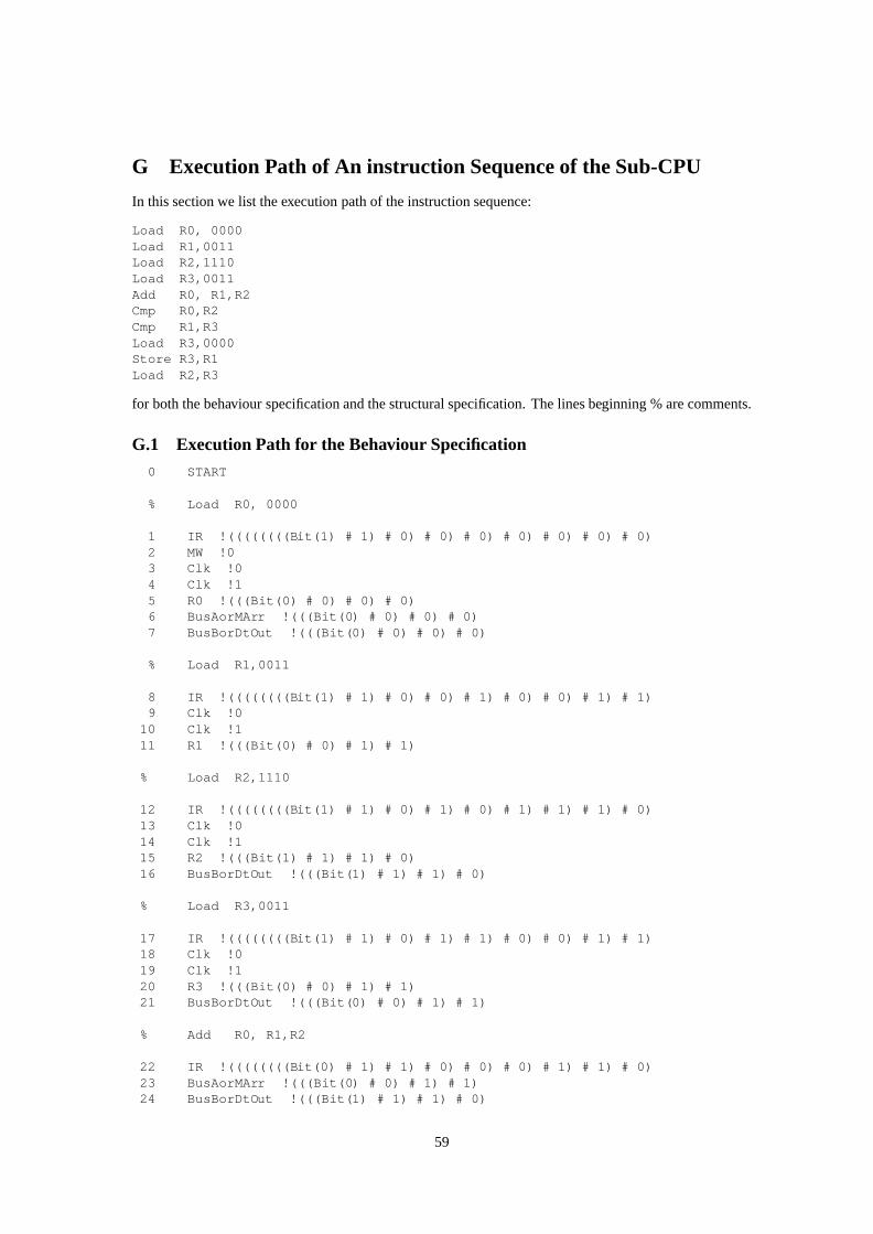
G ExecutionPath of An instruction Sequenceof the Sub-CPU
In thissectionwe list theexecutionpathof theinstructionsequence:
Load R0, 0000Load R1,0011Load R2,1110Load R3,0011Add R0, R1,R2Cmp R0,R2Cmp R1,R3Load R3,0000Store R3,R1Load R2,R3
for boththebehaviour specificationandthestructuralspecification.Thelinesbeginning% arecomments.
G.1 ExecutionPath for the Behaviour Specification
0 START
% Load R0, 0000
1 IR !((((((((B it (1) # 1) # 0) # 0) # 0) # 0) # 0) # 0) # 0)2 MW !03 Clk !04 Clk !15 R0 !(((Bit(0) # 0) # 0) # 0)6 BusAorMAr r !(((Bit(0 ) # 0) # 0) # 0)7 BusBorDtO ut !(((Bit( 0) # 0) # 0) # 0)
% Load R1,0011
8 IR !((((((((B it (1) # 1) # 0) # 0) # 1) # 0) # 0) # 1) # 1)9 Clk !0
10 Clk !111 R1 !(((Bit(0) # 0) # 1) # 1)
% Load R2,1110
12 IR !((((((((B it (1) # 1) # 0) # 1) # 0) # 1) # 1) # 1) # 0)13 Clk !014 Clk !115 R2 !(((Bit(1) # 1) # 1) # 0)16 BusBorDtO ut !(((Bit( 1) # 1) # 1) # 0)
% Load R3,0011
17 IR !((((((((B it (1) # 1) # 0) # 1) # 1) # 0) # 0) # 1) # 1)18 Clk !019 Clk !120 R3 !(((Bit(0) # 0) # 1) # 1)21 BusBorDtO ut !(((Bit( 0) # 0) # 1) # 1)
% Add R0, R1,R2
22 IR !((((((((B it (0) # 1) # 1) # 0) # 0) # 0) # 1) # 1) # 0)23 BusAorMAr r !(((Bit(0 ) # 0) # 1) # 1)24 BusBorDtO ut !(((Bit( 1) # 1) # 1) # 0)
59
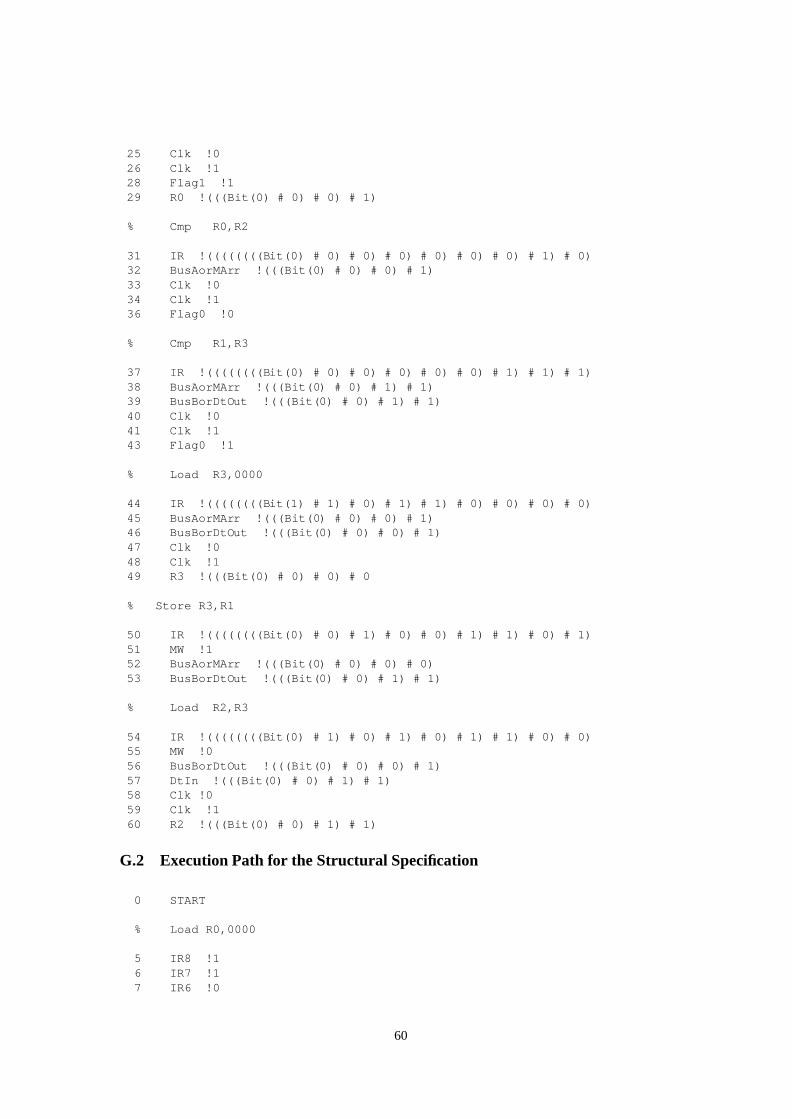
25 Clk !026 Clk !128 Flag1 !129 R0 !(((Bit(0) # 0) # 0) # 1)
% Cmp R0,R2
31 IR !((((((((B it (0) # 0) # 0) # 0) # 0) # 0) # 0) # 1) # 0)32 BusAorMAr r !(((Bit(0 ) # 0) # 0) # 1)33 Clk !034 Clk !136 Flag0 !0
% Cmp R1,R3
37 IR !((((((((B it (0) # 0) # 0) # 0) # 0) # 0) # 1) # 1) # 1)38 BusAorMAr r !(((Bit(0 ) # 0) # 1) # 1)39 BusBorDtO ut !(((Bit( 0) # 0) # 1) # 1)40 Clk !041 Clk !143 Flag0 !1
% Load R3,0000
44 IR !((((((((B it (1) # 1) # 0) # 1) # 1) # 0) # 0) # 0) # 0)45 BusAorMAr r !(((Bit(0 ) # 0) # 0) # 1)46 BusBorDtO ut !(((Bit( 0) # 0) # 0) # 1)47 Clk !048 Clk !149 R3 !(((Bit(0) # 0) # 0) # 0
% Store R3,R1
50 IR !((((((((B it (0) # 0) # 1) # 0) # 0) # 1) # 1) # 0) # 1)51 MW !152 BusAorMAr r !(((Bit(0 ) # 0) # 0) # 0)53 BusBorDtO ut !(((Bit( 0) # 0) # 1) # 1)
% Load R2,R3
54 IR !((((((((B it (0) # 1) # 0) # 1) # 0) # 1) # 1) # 0) # 0)55 MW !056 BusBorDtO ut !(((Bit( 0) # 0) # 0) # 1)57 DtIn !(((Bit( 0) # 0) # 1) # 1)58 Clk !059 Clk !160 R2 !(((Bit(0) # 0) # 1) # 1)
G.2 ExecutionPath for the Structural Specification
0 START
% Load R0,0000
5 IR8 !16 IR7 !17 IR6 !0
60
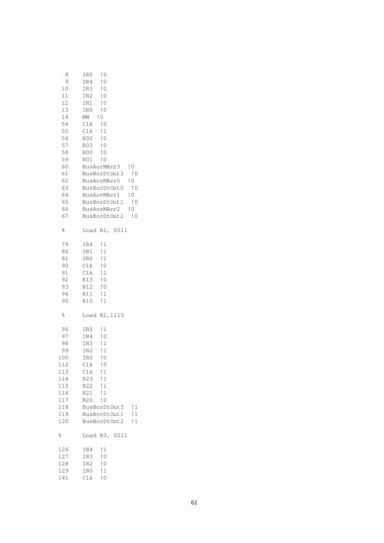
8 IR5 !09 IR4 !0
10 IR3 !011 IR2 !012 IR1 !013 IR0 !014 MW !054 Clk !055 Clk !156 R02 !057 R03 !058 R00 !059 R01 !060 BusAorMAr r3 !061 BusBorDtO ut3 !062 BusAorMAr r0 !063 BusBorDtO ut0 !064 BusAorMAr r1 !065 BusBorDtO ut1 !066 BusAorMAr r2 !067 BusBorDtO ut2 !0
% Load R1, 0011
79 IR4 !180 IR1 !181 IR0 !190 Clk !091 Clk !192 R13 !093 R12 !094 R11 !195 R10 !1
% Load R2,1110
96 IR5 !197 IR4 !098 IR3 !199 IR2 !1
100 IR0 !0112 Clk !0113 Clk !1114 R23 !1115 R22 !1116 R21 !1117 R20 !0118 BusBorDtO ut3 !1119 BusBorDtO ut1 !1120 BusBorDtO ut2 !1
% Load R3, 0011
126 IR4 !1127 IR3 !0128 IR2 !0129 IR0 !1141 Clk !0
61

142 Clk !1143 R33 !0144 R32 !0145 R31 !1146 R30 !1147 BusBorDtO ut3 !0148 BusBorDtO ut2 !0149 BusBorDtO ut0 !1
% ADD R0,R1,R2
153 IR8 !0154 IR6 !1155 IR5 !0156 IR4 !0157 IR2 !1158 IR0 !0171 BusAorMAr r0 !1172 BusBorDtO ut3 !1173 BusAorMAr r1 !1174 BusBorDtO ut0 !0175 BusBorDtO ut2 !1195 Clk !0196 Clk !1197 Flag1 !1198 R00 !1
% CMP R0,R2
199 IR7 !0200 IR6 !0201 IR2 !0205 IR0 !0209 BusAorMAr r1 !0234 Clk !0235 Clk !1236 Flag0 !1
% CMP R1,R3
237 IR2 !1238 IR0 !1243 BusBorDtO ut3 !0244 BusAorMAr r1 !1245 BusBorDtO ut2 !0246 BusBorDtO ut0 !1253 Clk !0254 Clk !1255 Flag0 !0
% Load R3,0000
256 IR8 !1257 IR7 !1258 IR5 !1259 IR4 !1260 IR2 !0261 IR1 !0
62

262 IR0 !0274 BusAorMAr r1 !0275 BusBorDtO ut1 !0278 Clk !0279 Clk !1280 R30 !0281 R31 !0
% Store R3,R1
282 IR8 !0283 IR7 !0284 IR6 !1285 IR5 !0286 IR4 !0287 IR3 !1288 IR2 !1289 IR0 !1291 MW !1302 BusAorMAr r0 !0303 BusBorDtO ut1 !1316 Clk !0317 Clk !1
% Load R2,R3
318 IR7 !1319 IR6 !0320 IR5 !1321 IR0 !0323 MW !0331 BusBorDtO ut1 !0339 DtIn3 !0340 DtIn2 !0341 DtIn1 !1342 DtIn0 !1345 Clk !0346 Clk !1347 R22 !0348 R23 !0349 R20 !1
63


![arXiv:0711.0769v1 [hep-ex] 5 Nov 20072 25Department of Physics and Astronomy, University of South Carolina, Columbia, South Carolina 29208, USA 26Department of Physics, Stanford University,](https://img.dokumen.tips/doc/110x75/6066fb08f64a8a679c5d6d37/arxiv07110769v1-hep-ex-5-nov-2007-2-25department-of-physics-and-astronomy-university.jpg)