Embed Size (px)
Citation preview

Institutionen för systemteknikDepartment of Electrical Engineering
Examensarbete
Study of Interferer Canceling Systems in a SoftwareDefined Radio Receiver
Examensarbete utfört i Radioelektronikvid Tekniska högskolan vid Linköpings universitet
av
Oskar Holstensson
LiTH-ISY-EX--12/4650--SE
Linköping 2013
Department of Electrical Engineering Linköpings tekniska högskolaLinköpings universitet Linköpings universitetSE-581 83 Linköping, Sweden 581 83 Linköping

Study of Interferer Canceling Systems in a SoftwareDefined Radio Receiver
Examensarbete utfört i Radioelektronikvid Tekniska högskolan vid Linköpings universitet
av
Oskar Holstensson
LiTH-ISY-EX--12/4650--SE
Handledare: Nicolas RegimbalAtlantic Innovation Electronic Solutions
Examinator: Ted Johanssonisy, Linköpings universitet
Linköping, 22 maj 2013


Avdelning, InstitutionDivision, Department
Electronic DevicesDepartment of Electrical EngineeringSE-581 83 Linköping
DatumDate
2013-05-22
SpråkLanguage
� Svenska/Swedish
� Engelska/English
�
�
RapporttypReport category
� Licentiatavhandling
� Examensarbete
� C-uppsats
� D-uppsats
� Övrig rapport
�
�
URL för elektronisk version
http://urn.kb.se/resolve?urn=urn:nbn:se:liu:diva-92757
ISBN
—
ISRN
LiTH-ISY-EX--12/4650--SE
Serietitel och serienummerTitle of series, numbering
ISSN
—
TitelTitle
Studie av Störsignalsneutraliserande System i en Mjukvarudefinierad Radiomottagare
Study of Interferer Canceling Systems in a Software Defined Radio Receiver
FörfattareAuthor
Oskar Holstensson
SammanfattningAbstract
This thesis describes the work related to an interferer rejection system employing frequencyanalysis and cancellation through phase-opposed signal injection. The first device in thefrequency analysis chain, an analog fast Fourier transform application-specific integratedcircuit (asic), was improved upon. The second device, a chained fast Fourier transformfollowed by a frequency analysis module employing cross-correlation for signal detectionwas specified, designed and implemented in vhdl.
NyckelordKeywords ASIC, FFT, Interferer Cancellation, RF, SDR, VHDL


Abstract
This thesis describes the work related to an interferer rejection system employ-ing frequency analysis and cancellation through phase-opposed signal injection.The first device in the frequency analysis chain, an analog fast Fourier transformapplication-specific integrated circuit (asic), was improved upon. The seconddevice, a chained fast Fourier transform followed by a frequency analysis mod-ule employing cross-correlation for signal detection was specified, designed andimplemented in vhdl.
vii


Acknowledgments
I want to express my gratitude to my supervisor Nicolas Regimbal for his helpfulguidance during the thesis.
Many thanks go to my examiner Ted Johansson for his support and never-endingsource of wisdom and patience.
I would also like to express my gratitude to my friends at the university, mostnotably my very good friend Christoffer Peters.
Finally I thank my loving family for always supporting me in whatever endeavorI submit to at the time.
ix

Contents
Notation xiii
I Background
1 Introduction 171.1 Leon and the interferer rejection system . . . . . . . . . . . . . . . 171.2 Goals . . . . . . . . . . . . . . . . . . . . . . . . . . . . . . . . . . . 181.3 Document outline . . . . . . . . . . . . . . . . . . . . . . . . . . . . 19
2 Software radio 212.1 Traditional radio receivers . . . . . . . . . . . . . . . . . . . . . . . 212.2 Software defined radio . . . . . . . . . . . . . . . . . . . . . . . . . 212.3 Cognitive radio . . . . . . . . . . . . . . . . . . . . . . . . . . . . . 222.4 This work . . . . . . . . . . . . . . . . . . . . . . . . . . . . . . . . . 23
II Results
3 The sasp 273.1 Introduction . . . . . . . . . . . . . . . . . . . . . . . . . . . . . . . 273.2 Analog processing modules . . . . . . . . . . . . . . . . . . . . . . 28
3.2.1 Analog adders . . . . . . . . . . . . . . . . . . . . . . . . . . 283.2.2 Delay line . . . . . . . . . . . . . . . . . . . . . . . . . . . . 283.2.3 Sample and hold . . . . . . . . . . . . . . . . . . . . . . . . 293.2.4 Weighting unit . . . . . . . . . . . . . . . . . . . . . . . . . . 293.2.5 Matrix unit . . . . . . . . . . . . . . . . . . . . . . . . . . . . 303.2.6 Sample selector . . . . . . . . . . . . . . . . . . . . . . . . . 30
3.3 Control modules . . . . . . . . . . . . . . . . . . . . . . . . . . . . . 313.3.1 Flip-flop . . . . . . . . . . . . . . . . . . . . . . . . . . . . . 313.3.2 Address generator . . . . . . . . . . . . . . . . . . . . . . . . 313.3.3 Coefficient control . . . . . . . . . . . . . . . . . . . . . . . 35
3.4 Results . . . . . . . . . . . . . . . . . . . . . . . . . . . . . . . . . . 38
xi

xii CONTENTS
3.5 Conclusions . . . . . . . . . . . . . . . . . . . . . . . . . . . . . . . 413.5.1 Future work . . . . . . . . . . . . . . . . . . . . . . . . . . . 41
4 Frequency analysis and the dsp 434.1 Theory . . . . . . . . . . . . . . . . . . . . . . . . . . . . . . . . . . 434.2 Feasibility test . . . . . . . . . . . . . . . . . . . . . . . . . . . . . . 44
4.2.1 Algorithm . . . . . . . . . . . . . . . . . . . . . . . . . . . . 454.2.2 Results . . . . . . . . . . . . . . . . . . . . . . . . . . . . . . 45
4.3 rtl implementation . . . . . . . . . . . . . . . . . . . . . . . . . . . 494.3.1 Buffer . . . . . . . . . . . . . . . . . . . . . . . . . . . . . . . 504.3.2 fft . . . . . . . . . . . . . . . . . . . . . . . . . . . . . . . . 504.3.3 Frequency analyzer . . . . . . . . . . . . . . . . . . . . . . . 534.3.4 Compensator . . . . . . . . . . . . . . . . . . . . . . . . . . 574.3.5 Results . . . . . . . . . . . . . . . . . . . . . . . . . . . . . . 57
4.4 Conclusions . . . . . . . . . . . . . . . . . . . . . . . . . . . . . . . 594.4.1 Future work . . . . . . . . . . . . . . . . . . . . . . . . . . . 594.4.2 Multiple signal detection . . . . . . . . . . . . . . . . . . . . 594.4.3 Solving ambiguities . . . . . . . . . . . . . . . . . . . . . . . 59
5 Summary 615.1 Conclusions . . . . . . . . . . . . . . . . . . . . . . . . . . . . . . . 615.2 Future work . . . . . . . . . . . . . . . . . . . . . . . . . . . . . . . 625.3 Final words . . . . . . . . . . . . . . . . . . . . . . . . . . . . . . . . 62
Bibliography 65
A Signal detection with cross-correlation 67
B Fast Fourier transform 71B.1 Decimation-in-time radix-4 FFT . . . . . . . . . . . . . . . . . . . . 71B.2 Decimation-in-frequency radix-4 FFT . . . . . . . . . . . . . . . . . 75

Notation
Abbreviations
Abbreviation Meaning
adc Analog to Digital Converteraft Analog Fourier Transformasic Application-Specific Integrated Circuitcmos Complementary Metal Oxide Semiconductordac Digital to Analog Converterdft Discrete Fourier Transformdsp Digital Signal Processorfft Fast Fourier Transformfpga Field Programmable Gate Arrayfsm Finite State Machinemac Multiply And Accumulaterom Read-Only Memoryrtl Register-Transfer Levelsasp Sampled Analog Signal Processorsdr Software Defined Radiosr Software Radiovhdl vhsic Hardware Description Languagevhf Very High Frequencyvhsic Very-High-Speed Integrated Circuit
xiii


Part I
Background


1Introduction
This thesis was carried out at Atlantic Innovation Electronic Solutions in Bor-deaux with the aim of studying and implementing the interferer cancellation sys-tem proposed in the Leon project, discussed later in this chapter. It was done inthe scope of a master’s thesis project of 20 weeks in the spring of 2012.
The present work has been led in the framework of the ITP SIMCLAIRS com-peted program. France, United Kingdom and Sweden have mandated the Euro-pean Defence Agency (EDA) to contract the Project with a Consortium composedof THALES SYSTEMES AEROPORTES France, acting as the Consortium Leader,SELEX Galileo Ltd, THALES UK Ltd and SAAB AB.
1.1 Leon and the interferer rejection system
Leon is a project supervised by Atlantic Innovation Electronic Solutions. Theproject aims at creating an interferer rejection system using the sampled analogsignal processor, or sasp, described below. The goal is to be able to cancel outany wideband signal from the vhf to Ku bands, or 30 MHz to 18 GHz.
The system makes use of frequency analysis of the input signal to distinguishpowerful interferers, and superimposes a phase-opposed signal on top of the in-put signal, delayed through a delay line. An overview of the system is depictedin figure 1.1.
For frequency analysis, the input signal is processed using an analog Fouriertransform. The algorithm is the popular radix-4 fast Fourier transform (fft) al-gorithm by Cooley and Tukey (1965).
To enhance the frequency resolution, the dsp itself performs another fft. A dig-
17

18 1 Introduction
Figure 1.1: Proposed system
ital signal processing unit then processes the output of the second transform todetermine the frequency, amplitude and phase of any interfering signals. If thefrequency resolution following the analog Fourier transform is sufficient, thenthe cascaded transform can be omitted, but then the aftmust supply a spectrumexcerpt for analysis.
The purpose of the analog delay line is to delay the signal while its spectral con-tents are being determined, and phase-opposed rejection signals are being cre-ated. When the signal exits the delay line, the rejection signals are added tocancel out the interferers.
The sampled analog signal processor, or sasp, was created at lab IMS in Bor-deaux by Dr. Rivet (2009) for his doctor’s thesis. The signal processor performsa Fourier transform on the incoming radio signal, allowing for isolation of indi-vidual frequency components, and simplifying subsequent signal processing. Aproof-of-concept sasp was created, capable of continuously sustaining 64-pointFourier transforms at a sampling frequency of 640 MHz.
Analyzing the incoming spectrum with the help of the sasp, interfering signalsare detected and have their phase-opposed equivalents superimposed over them.With accurate enough analysis of the incoming spectrum, this will effectivelycancel the interferers. However, the limitation to 64-point transforms provesproblematic. The possibility of performing a chained Fourier transform afterthat of the sasp has been examined, with a proof-of-concept Matlab model. Thisimproves the precision of the analysis, but also comes with a new set of issues.
1.2 Goals
This work has a clear divide between two tasks, and consequently its goals comesin these two parts.
• First, the requirements of the digital signal processing will be analyzed andimplemented in vhdl.

1.3 Document outline 19
• Second, the work on the sasp will be resumed and advanced towards itscompletion.
The first goal is open for different approaches and architectures. The secondgoal, in that it involves a project resumed at a late stage of development, is morerestricted and has the following requirements.
• Maximum chip area: 1.44 mm2
• Maximum power consumption: 100 mW
• Minimum speed: 2 GHz
The two tasks stated above are in the chronological order in which the goals wereidentified and performed. However, for the sake of narrative, this report reordersthem in the order in which they appear in the system.
1.3 Document outline
Chapter 2 discusses modern radio receiver challenges and presents the conceptof software defined radio.
In chapter 3, the work on improving the sasp is presented. The different buildingblocks, analog and digital, are presented and the work done on them during thisthesis is highlighted.
In chapter 4, the subject of chaining Fourier transforms is discussed. The issueswith inaccuracy involved in this method of spectral analysis are presented, andsolutions to these problems are discussed. The chapter presents a comprehensiveworkflow from mathematical concept to a Matlab model and ending in a synthe-sizable vhdlmodel.
Finally, a summary and conclusive remarks are found in chapter 5.

2Software radio
This chapter briefly brings up the topic of traditional radio and moves towardsthe concept of the software radio, setting the background of the work.
2.1 Traditional radio receivers
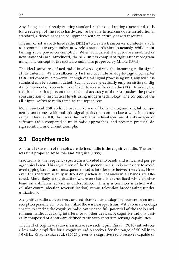
Traditional radio receivers work by tuning in to a certain channel in the wantedband. The radio signal from the antenna is amplified through a low-noise ampli-fier. Signals in other channels and even other bands need to be filtered out, andare often done so at an intermediate frequency.
However, an interferer of sufficient power risk saturating the low-noise amplifierand might even damage it. Employing a tuned antenna or RF filters attenuatesinterferers out of band, and in-band interferers are already assumed to behaveaccording to the corresponding standard.
These steps to minimize the damage caused by interferers greatly reduce the tun-ability of the circuit. Highly configurable RF filters of sufficient quality are verydifficult to construct. To keep the cost and power consumption at a minimum,radio receivers are highly tuned and the entire signal path is optimized for thetarget specification.
2.2 Software defined radio
The high specialization of radio receiver circuits prohibits them from sharingmore than a fraction of their signal paths. This leads to device complexity grow-ing with the number of communication standards accommodated.
21
22 2 Software radio
Any change in an already existing standard, such as a allocating a new band, callsfor a redesign of the radio hardware. To be able to accommodate an additionalstandard, a device needs to be upgraded with an entirely new transceiver.
The aim of software defined radio (sdr) is to create a transceiver architecture ableto accommodate any number of wireless standards simultaneously, while main-taining a low power consumption. When concurrent standards are modified ornew standards are introduced, the sdr unit is compliant right after reprogram-ming. The concept of the software radio was proposed by Mitola (1995).
The ideal software defined radio involves digitizing the incoming radio signalat the antenna. With a sufficiently fast and accurate analog-to-digital converter(adc) followed by a powerful enough digital signal processing unit, any wirelessstandard can be accommodated. Such a device, practically only consisting of dig-ital components, is sometimes referred to as a software radio (sr). However, therequirements this puts on the speed and accuracy of the adc pushes the powerconsumption to impractical levels using modern technology. The concept of theall-digital software radio remains an utopian one.
More practical sdr architectures make use of both analog and digital compo-nents, sometimes with multiple signal paths to accommodate a wide frequencyrange. Deval (2010) discusses the problems, advantages and disadvantages ofsoftware radio compared to multi-radio approaches, and presents practical de-sign solutions and circuit examples.
2.3 Cognitive radio
A natural extension of the software defined radio is the cognitive radio. The termwas first proposed by Mitola and Maguire (1999).
Traditionally, the frequency spectrum is divided into bands and is licensed per ge-ographical area. This regulation of the frequency spectrum is necessary to avoidoverlapping bands, and consequently evades interference between services. How-ever, the spectrum is fully utilized only when all channels in all bands are allo-cated. More likely is the situation where one band is overutilized while anotherband on a different service is underutilized. This is a common situation withcellular communication (overutilization) versus television broadcasting (under-utilization).
A cognitive radio detects free, unused channels and adapts its transmission andreception parameters to better utilize the wireless spectrum. With accurate enoughspectrum sensing the cognitive radio can use the full potential of the radio envi-ronment without causing interference to other devices. A cognitive radio is basi-cally composed of a software defined radio with spectrum sensing capabilities.
The field of cognitive radio is an active research topic. Razavi (2010) introducesa low-noise amplifier for a cognitive radio receiver for the range of 50 MHz to10 GHz. Kitsunezuka et al. (2012) presents a cognitive radio receiver capable of

2.4 This work 23
receiving signals between 30 MHz and 2.4 GHz. It is also able to sense spectralenergy to determine band availability.
2.4 This work
The ultimate goal in the Leon project is to cancel powerful interferer signals fromthe vhf to Ku bands, or 30 MHz to 18 GHz. At this bandwidth any single filter isnot feasible, and accommodating all possible blocker profiles is highly unfeasible.
The Leon project is designed to accommodate any radio receiver operation, andtargets no specific application or radio standard. The project is in other wordseffectively a flexible filter, directly appropriate for use in an sdr or cognitiveradio receiver.


Part II
Results


3The SASP
3.1 Introduction
The sampled analog signal processor, or the sasp, is a device that is capable ofperforming a Fourier transform with analog samples, or analog Fourier transform(aft). It was created at lab IMS in Bordeaux by Dr. Rivet (2009) for his doctor’sthesis.
In Leon, the sasp performs the first of two cascaded Fourier transforms. It islocated at the input (figure 3.1).
Figure 3.1: The aft in the proposed system
The sasp performs a sample-and-hold operation on the input signal, and thenutilizes a series of delay lines and analog arithmetic units to perform the division-in-time radix-4 fast Fourier transform by Cooley and Tukey (1965), derived insection B.1. One frequency bin of the operation is selected and its complex analog
27
28 3 The sasp
value is output each time the transform has completed.
The chosen architecture has the advantage of being able to operate continuously.It inputs one sample and outputs one frequency bin per clock cycle.
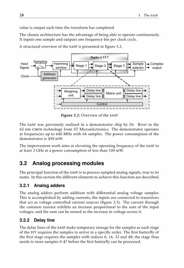
A structural overview of the sasp is presented in figure 3.2.
Figure 3.2: Overview of the sasp
The sasp was previously realized in a demonstrator chip by Dr. Rivet in the65 nm cmos technology from ST Microelectronics. The demonstrator operatesat frequencies up to 640 MHz with 64 samples. The power consumption of thedemonstrator is 450 mW.
The improvement work aims at elevating the operating frequency of the sasp toat least 2 GHz at a power consumption of less than 100 mW.
3.2 Analog processing modules
The principal function of the sasp is to process sampled analog signals, true to itsname. In this section the different elements to achieve this function are described.
3.2.1 Analog adders
The analog adders perform addition with differential analog voltage samples.This is accomplished by adding currents; the inputs are connected to transistorsthat act as voltage controlled current sources (figure 3.3). The current throughthe common resistor exhibits an increase proportional to the sum of the inputvoltages, and the sum can be sensed as the increase in voltage across it.
3.2.2 Delay line
The delay lines of the saspmake temporary storage for the samples as each stageof the fft requires the samples to arrive in a specific order. The first butterfly ofthe first stage requires the samples with indices 0, 16, 32 and 48; the stage thusneeds to store samples 0-47 before the first butterfly can be processed.

3.2 Analog processing modules 29
bias
apos aneg bnegbpos
bias
Vdd
outpos
outneg
Figure 3.3: Analog two-input adder
Furthermore, the delay lines play a role in the deserialization and serializationof the samples. At the input of each stage, one sample arrives per clock cycle,but the matrix unit processes four samples at a time. The output delay line thenserializes the samples so that they are again sent to the next stage at a rate of onesample per clock cycle.
3.2.3 Sample and hold
At the input of the sasp, the sample and hold circuit converts the continuous-time input signal to a discrete-time one suitable for processing.
3.2.4 Weighting unit
Both windowing and the fft algorithm require the input samples to be multi-plied with certain coefficients. For the sasp, this is accomplished in the weightingunit. It is based on the work by Abiven (2011). The device effectively multipliesan analog sample with a digital value.
The architecture was improved in this thesis. The previous architecture utilized abase-10 approach, providing 100 possible digital values with eight control lines.This approach is called binary coded decimal and was chosen as it is clear andintuitive when programming by hand.
As the coefficients were to be provided by a read-only memory (rom) structurethat can be programmed automatically, a pure binary approach was chosen in-stead. This increased the number of values to 256.
The multiplication is accomplished by scaling the input by factors of 2−k , k =0, 1, 2, . . . , 7, and then adding a subset of these together. The subset is determinedby the bits in the digital factor.

30 3 The sasp
c =7∑n=0
2−n (3.1)
The largest possible coefficient is 2 − 2−7, and its use is considered as scaling theinput by unity.
Multiplying complex numbers is accomplished by using four real-valued weight-ing units and two two-input analog adders as shown in equation 3.2.
<{out} =<{a} ∗<{b} −={a} ∗={b}={out} =={a} ∗<{b} +<{a} ∗={b}
(3.2)
3.2.5 Matrix unit
The matrix unit implements the addition matrix derived in section B.1. Equa-tion B.6 is included here for clarity.
X(k)
X(k + N4 )
X(k + N2 )
X(k + 3N4 )
=
1 1 1 1
1 −j −1 j
1 −1 1 −1
1 j −1 −j
1
W kN
W 2kN
W 3kN
ᵀ F0(k)
F1(k)
F2(k)
F3(k)
ᵀ
The trivial multiplications by factors −j,−1 and j are performed by simply rewiringthe differential analog signals at the input of the analog adders.
3.2.6 Sample selector
The sample selector waits at the end of the pipeline, and grabs one specific fre-quency bin every time it appears at the output. The frequency bin to be selectedis programmable by specifying the corresponding binary number at 6 input pins.
After the sample selector is a set of buffers to drive the output pins of the chip.These buffers have an extended output swing to facilitate chip measurement.
3.3 Control modules 31
3.3 Control modules
To control the workflow and provide coefficients for the analog weighting units, aset of control modules are required. This section presents the principal modulesand their function.
The modules described here were all designed and implemented during this the-sis.
3.3.1 Flip-flop
Digital flip-flops are used to store the digital values used for controlling the sasp.The selected architecture is that of Yuan and Svensson (1989). The chosen ar-chitecture was selected due to its simplicity; it does not require complementaryclock phases.
The architecture is dynamic and will lose its data unless a minimum clock speedis maintained. This is the digital equivalent of the delay line cell. The schematicand layout of the flip-flop is depicted in figure 3.4 and figure 3.5 respectively.
Vdd
in
out
clk
clk
clk
clk
Figure 3.4: Flip-flop schematic Figure 3.5: Flip-flop layout
3.3.2 Address generator
To control the sasp, an address generator unit is used. It contains a 6-bit counterto provide a global state followed by adders to compensate for phase differencesin the different stages of processing.
Since the contents of the rom modules are easily manipulated, their contentscan be shifted to obtain a virtual phase shift. Moreover, the phase difference ofthe sample selector can be compensated off-chip. By utilizing these techniques,the Hamming window unit, stage 1 and the sample selector all run on the baseaddress of the address generator, saving space and power. Stages 2 and 3 run onaddresses with their own phase adjustments.
The counter and adder architectures are that of Kogge-Stone adders (Kogge andStone, 1973). Stages 2 and 3 have hard-coded offsets to provide the requiredphase difference. The Kogge-Stone architecture was selected because of the speed

32 3 The sasp
requirements; the adders need to operate reliably at 2 GHz. Simple carry-chainadders proved to be too slow for the application, even for as few as 6 bits.
Adding two binary numbers the pen-and-paper way, one begins the addition atthe rightmost bits. If both bits are 1, a value of one carries over to the left. Thealgorithm then proceeds to the next bit position, adding the bits at that positiontogether with any carried bit. This is repeated for all bits.
The problem with this algorithm is that it forms a chain of carried bits, and thefinal outcome will have to wait until this long chain is fully traversed. To speedup this process, carry-lookahead is performed.
For each pair of bits of the inputs, An and Bn, n = 0, 1, . . . , N − 1, two propertiesare derived.
• If An and Bn are both 1, then a bit will be carried to the left regardless ofwhether a carry arrives from the right. This property is called generate, orGn.
• If only one of An or Bn is 1, then a bit will be carried if and only if a carryarrives from the right. This property is called propagate, or Pn.
These two properties are calculated as a first step. Secondly, these properties arecalculated for all pairs of two consecutive positions of the inputs. For positions nand n − 1, this group of bits is set to generate if bit n already generates (Gn = 1),or if bit n − 1 is set to generate while bit n is set to propagate that bit. The entiregroup of bits is set to propagate if both bits of the sequence propagate.
Extending these definitions for any group of bits running from n tom, their cumu-lative generate and propagate properties are called Gn↔m and Pn↔m respectively.
The cumulative properties can be extended, always including one bit to see ifthe extended group is set to generate or propagate. However, a lot of redundantprocessing is avoided by instead taking the generate and propagate properties ofa group, and combining it with the largest adjoining group that has already beenresolved.
Ultimately this will determine Gn↔0 and Pn↔0 for all bit positions n. Since eachprocessing step can effectively double the group length, a total of log2 N process-ing steps are required.
When a group has the propagate property, it will propagate to the left any carriedbit from the right. However, when the cumulative properties are known all theway to the least significant bit (bit 0), there is no possibility of a carry bit arrivingfrom the right. The generate property then unambiguously determines whetherthe group already has generated a carry bit or not. Now all the complete groupsgenerate a carry bit to the left if and only if it has the generate property, that is,Cn = Gn−1↔0.
To arrive at the sum, the three bits An, Bn and Cn are added to form the sumbit, Sn = An ⊕ Bn ⊕ Cn. Leveraging an optimization, it is possible to reuse the

3.3 Control modules 33
Pn property; since Pn = An ⊕ Bn it is possible to reduce the sum calculation toSn = Pn ⊕ Cn.
The phase-compensated addresses are converted to base-4, decoding each pair ofbinary bits into four lines. This goes well with the radix-4 design of the fft imple-mentation, and also reduces the complexity of the coefficient rom architecture.
pprev
Vdd
pprev
p
p
pout
Figure 3.6: Calculate Pschematic Figure 3.7: Calculate P layout
Calculate P and calculate G circuits were created and laid out. The schematicand layout for calculate P is shown in figure 3.6 and figure 3.7 respectively. Theschematic and layout for calculate G is shown in figure 3.8 and figure 3.9 respec-tively.
Vdd
gprev
gprev
g
g
p
p
gout
Figure 3.8: Calculate Gschematic Figure 3.9: Calculate G layout
Using the above structures, a matrix performing all of the reductions was cre-ated and laid out. The final layout for the structure calculating the cumulativegenerate property is shown in figure 3.10. The input to the circuit is at the topterminals, and the output is routed from the bottom.
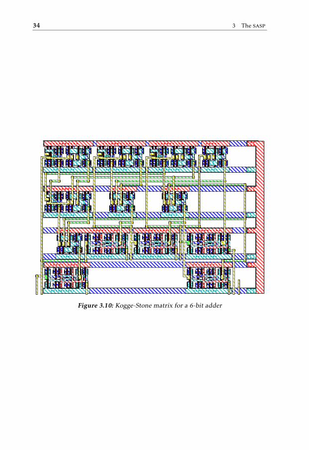
34 3 The sasp
Figure 3.10: Kogge-Stone matrix for a 6-bit adder

3.3 Control modules 35
3.3.3 Coefficient control
The Hamming window unit, stage 2 and stage 3 all require digital coefficientsfor their weighting units. These coefficients are supplied by use of a NOR romstructure, as seen in figure 3.11.
precharge
word line 0
word line 1
word line 2
Vdd Vdd Vdd
bit line 0 bit line 1 bit line 2
Figure 3.11: rom principle
Each word line is controlled by a small logic unit. It activates during one half ofthe clock cycle when the right address is supplied. During the other half of theclock cycle the bit lines are charged to VDD by pull-up transistors.
The contents of the rom is indicated by the presence of absence of a pull-downtransistor. When a word line is activated, the presence of a transistor at the junc-tion between said word line and a bit line will pull the corresponding bit linetowards ground, signifying a logical zero at this address. The bit lines withouttransistors in the active junction will remain at VDD , signifying a logical one. Thecontents of the 3x3 example rom depicted in figure 3.11 is 010, 101 and 111 ataddresses 0, 1 and 2 respectively.
The bit lines are heavily exposed to parasitic capacitance, and are therefore veryslow. To accurately read the value of the bit lines at each cycle a clocked sensorapproach is used.
When a bit line voltage drops below a reference voltage, nominally 200 mV belowVDD , an internal node is quickly discharged. This signifies a logical zero. If thebit line voltage is kept high, the internal node is kept undischarged and a logicalone is implied. At the end of the discharge phase, the logical value is forwardedto the output of the sensor.
The schematic and layout of the sensor is depicted in figure 3.12 and figure 3.13respectively.

36 3 The sasp
The layout of the coefficient rom for the last stage of the sasp is depicted infigure 3.14. The address is input from the right and the data is output to the left.
Vdd
ref bit line
out
clk
clk
clk
clk
Figure 3.12: rom sensor schematic
Figure 3.13: rom sensor layout

3.3 Control modules 37
Figure 3.14: Coefficient rom for the last stage of the sasp

38 3 The sasp
3.4 Results
The address generator was validated by post-layout simulation at 3 GHz to guar-antee robustness at the nominal frequency of operation, 2 GHz.
The post-layout simulation puts the average current of the address generator at1.43 mA. Figure 3.15 shows the internal six-bit counter state.
Figure 3.15 shows the state of the internal address counter.
Figure 3.16 shows the base-4 address of the Hamming window unit and stage 1.It is a delayed version of the internal address with each pair of bits decoded intothe equivalent base-4 digit.
Figure 3.17 shows the base-4 address of stage 2. This address enjoys a phase offsetin addition to being delayed and decoded into three base-4 digits.
Clock
Bit 1
Bit 2
Bit 3
Bit 4
Bit 5
Bit 6
Time (ns)
0 5 10 15 20
Figure 3.15: Address counter
All of the rom structures were verified by post-layout simulation. The largestrom, that of the last stage and the one depicted in figure 3.14, has an averagepower consumption of 4.25 mA.
The results show that the address generator is able to reliably provide addressesto all the blocks without discrepancies at up to 3 GHz.

3.4 Results 39
Digit 1 0 0 0 0 0 0 0 0 0 0 0 0 0 0 0 0 0 01 1 1 1 1 1 1 1 1 1 1 1 1 1 1 1 12 2 2 2 2 2 2 2 2 2 2 2 2 2 2 2 23 3 3 3 3 3 3 3 3 3 3 3 3 3 3 3 3 3
Digit 2 0 0 0 0 01 1 1 12 2 2 23 3 3 3
Digit 3 0 01 2 3
Time (ns)
0 5 10 15 20
Figure 3.16: Hamming window unit and stage 1 address
Digit 1 0 0 0 0 0 0 0 0 0 0 0 0 0 0 0 0 01 1 1 1 1 1 1 1 1 1 1 1 1 1 1 1 12 2 2 2 2 2 2 2 2 2 2 2 2 2 2 2 23 3 3 3 3 3 3 3 3 3 3 3 3 3 3 3 3 3
Digit 2 0 0 0 0 01 1 1 12 2 2 23 3 3 3 3
Digit 3 0 01 12 3
Time (ns)
0 5 10 15 20
Figure 3.17: Stage 2 address

40 3 The sasp
To test the finished modules, the entire Hamming window unit with coefficientrom was tested along with the address generator. The simulation includes theeffects of resistive and capacitive parasitics after layout. Figure 3.18 depicts theoutput of the Hamming window unit running at 3 GHz. The input to the weight-ing unit in this simulation is a constant voltage signal.
The output shows that the weighting unit is able to faithfully reconstruct theraised cosine that is the Hamming window. The address generator and the coeffi-cient rom supply the required control signals for it to work.
0 5 10 15 20
0
50
100
150
Time (ns)
Pot
entia
l (m
V)
Figure 3.18: Hamming window with new weighting unit architecture

3.5 Conclusions 41
3.5 Conclusions
At the end of the thesis, the work on the improved sasp had come a long way.The blocks that were worked on in this thesis; the address generator, coefficientrom blocks and the weighting unit, were finished. However, much work is stillrequired to provide for a completed circuit.
The constructed digital units include the rom architecture and the address gen-erator. These perform well under post-layout simulations up to 3 GHz, whilethe target speed is 2 GHz. This speed margin leaves room for some amount ofparasitic capacitance when routing the address signals across the chip, as well assome margin for fabrication. These blocks comprise the high-level control of allthe stages.
The weighting unit, arguably one of the most critical blocks in the system, worksreliably in simulations. It enjoys an improved architecture that paves the way formore linear behavior of the circuit.
As mentioned in section 1.2 in the introduction, the chip has power and arearequirements in addition to the 2 GHz speed requirement. Since the sasp wasnot fully finished, there was not yet any substantial area estimation, but an ap-proximation put the occupied area well below the limit. The power consumed bythe created blocks were moderate enough not to count substantially towards themaximum.
3.5.1 Future work
The delay lines of all the stages had their analog parts laid out even before thework of the thesis. However, still missing is the decoding circuitry, using the in-coming address to input or output samples in the correct order. The intimacy be-tween the delay lines and its control circuitry will inevitably lead to some amountof redesign of the analog architecture.
The input sample block as well as the sample selector (output) block needs to berealized and verified up to 2 GHz.
The area and power requirements need to be properly assessed; as the chip nearscompletion a power and area budget needs to be drawn up and followed through.
As a final task, the system will need to be assembled and verified by post-layoutsimulation including the entire chip die to guarantee satisfactory performanceup to the desired operating frequency.


4Frequency analysis and the DSP
In the Leon topology, the digital signal processor (dsp) takes care of the frequencyanalysis and forwards detected interferers to the signal generator (figure 4.1).The purpose is to increase the fidelity of the signal detection by further process-ing the sasp output to produce a more fine-grained spectrum followed by animproved signal detection algorithm.
This chapter looks into the theory and implementation of the frequency analysisand further highlights the improvements in the signal detection algorithm.
Figure 4.1: The dsp in the proposed system
4.1 Theory
The sasp performs a discrete Fourier transform (dft) using the fft algorithm forefficient computation.
43
44 4 Frequency analysis and the dsp
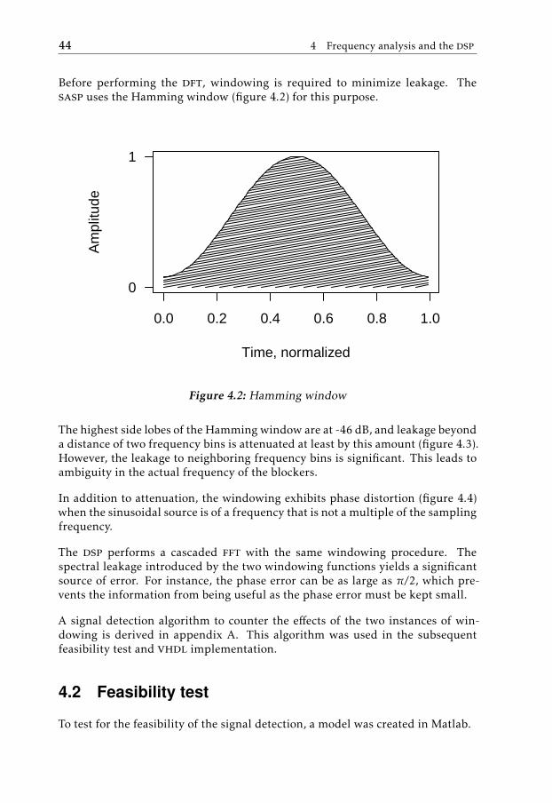
Before performing the dft, windowing is required to minimize leakage. Thesasp uses the Hamming window (figure 4.2) for this purpose.
0.0 0.2 0.4 0.6 0.8 1.0
Time, normalized
Am
plitu
de
0
1
Figure 4.2: Hamming window
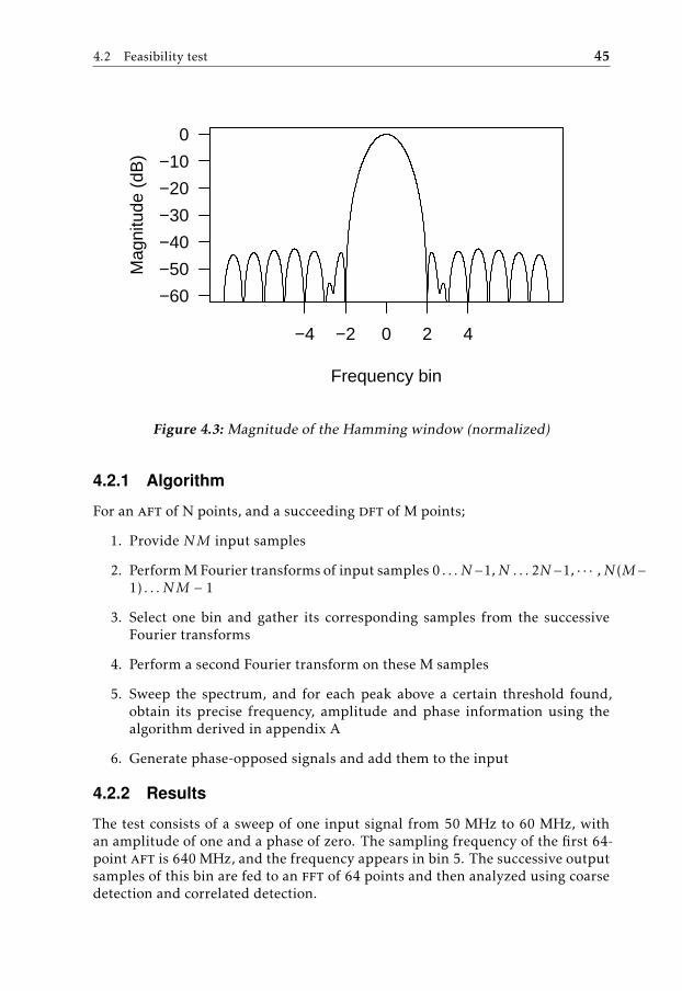
The highest side lobes of the Hamming window are at -46 dB, and leakage beyonda distance of two frequency bins is attenuated at least by this amount (figure 4.3).However, the leakage to neighboring frequency bins is significant. This leads toambiguity in the actual frequency of the blockers.
In addition to attenuation, the windowing exhibits phase distortion (figure 4.4)when the sinusoidal source is of a frequency that is not a multiple of the samplingfrequency.
The dsp performs a cascaded fft with the same windowing procedure. Thespectral leakage introduced by the two windowing functions yields a significantsource of error. For instance, the phase error can be as large as π/2, which pre-vents the information from being useful as the phase error must be kept small.
A signal detection algorithm to counter the effects of the two instances of win-dowing is derived in appendix A. This algorithm was used in the subsequentfeasibility test and vhdl implementation.
4.2 Feasibility test
To test for the feasibility of the signal detection, a model was created in Matlab.
4.2 Feasibility test 45
−60
−50
−40
−30
−20
−10
0
Frequency bin
Mag
nitu
de (
dB)
−4 −2 0 2 4
Figure 4.3: Magnitude of the Hamming window (normalized)
4.2.1 Algorithm
For an aft of N points, and a succeeding dft of M points;
1. Provide NM input samples
2. Perform M Fourier transforms of input samples 0 . . . N−1, N . . . 2N−1, · · · , N (M−1) . . . NM − 1
3. Select one bin and gather its corresponding samples from the successiveFourier transforms
4. Perform a second Fourier transform on these M samples
5. Sweep the spectrum, and for each peak above a certain threshold found,obtain its precise frequency, amplitude and phase information using thealgorithm derived in appendix A
6. Generate phase-opposed signals and add them to the input
4.2.2 Results
The test consists of a sweep of one input signal from 50 MHz to 60 MHz, withan amplitude of one and a phase of zero. The sampling frequency of the first 64-point aft is 640 MHz, and the frequency appears in bin 5. The successive outputsamples of this bin are fed to an fft of 64 points and then analyzed using coarsedetection and correlated detection.

46 4 Frequency analysis and the dsp
Frequency bin
Pha
se (
radi
ans)
−4 −2 0 2 4
− 3π− 2π
− π0
π2π3π
Figure 4.4: Phase of the Hamming window
50 54 58
0.80
0.85
0.90
0.95
1.00
1.05
1.10
Standard
Frequency (MHz)
Am
plitu
de
50 54 58
0.80
0.85
0.90
0.95
1.00
1.05
1.10
Correlated
Frequency (MHz)
Am
plitu
de
Figure 4.5: Detected amplitude
The Matlab model shows improved precision of the detected amplitude when thefrequency is not a multiple of the sampling frequency (figure 4.5).
In the case of the detected phase, just selecting the largest sample yields a phase
4.2 Feasibility test 47
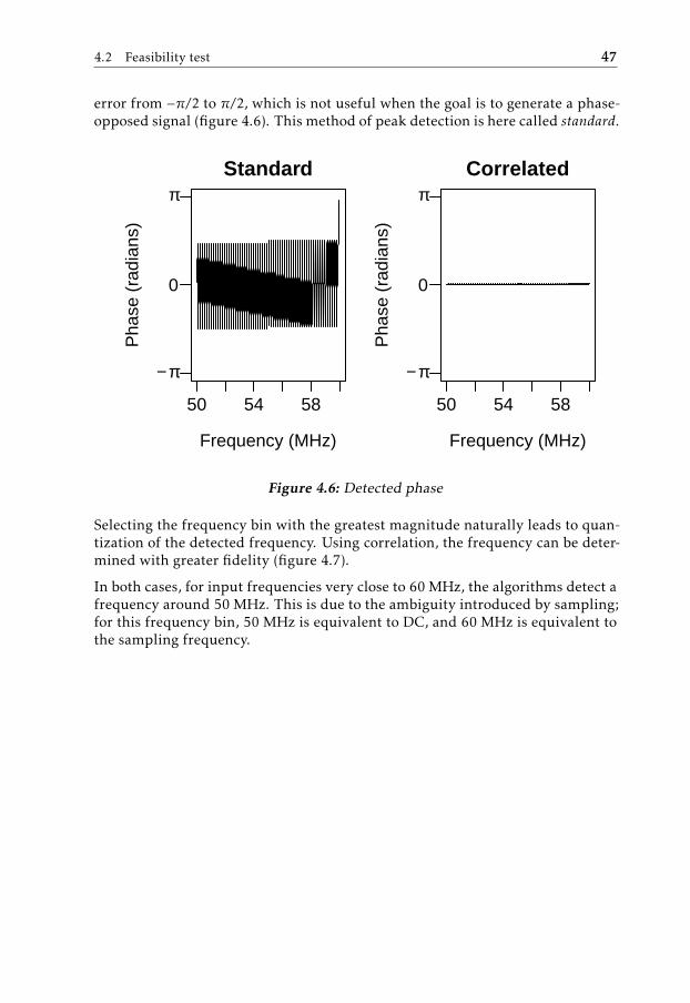
error from −π/2 to π/2, which is not useful when the goal is to generate a phase-opposed signal (figure 4.6). This method of peak detection is here called standard.
50 54 58
Standard
Frequency (MHz)
Pha
se (
radi
ans)
− π
0
π
50 54 58
Correlated
Frequency (MHz)
Pha
se (
radi
ans)
− π
0
π
Figure 4.6: Detected phase
Selecting the frequency bin with the greatest magnitude naturally leads to quan-tization of the detected frequency. Using correlation, the frequency can be deter-mined with greater fidelity (figure 4.7).
In both cases, for input frequencies very close to 60 MHz, the algorithms detect afrequency around 50 MHz. This is due to the ambiguity introduced by sampling;for this frequency bin, 50 MHz is equivalent to DC, and 60 MHz is equivalent tothe sampling frequency.

48 4 Frequency analysis and the dsp
50 54 58
−1.0
−0.5
0.0
0.5
1.0
Standard
Frequency (MHz)
Fre
quen
cy e
rror
(pe
rcen
tage
)
50 54 58
−1.0
−0.5
0.0
0.5
1.0
Correlated
Frequency (MHz)
Fre
quen
cy e
rror
(pe
rcen
tage
)
Figure 4.7: Frequency error
4.3 rtl implementation 49
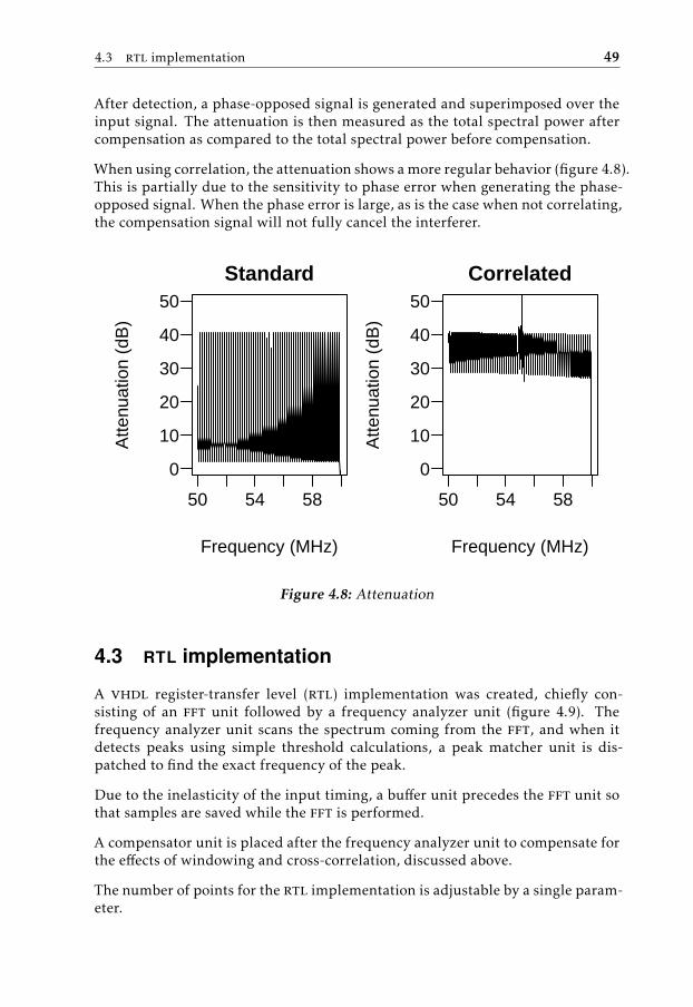
After detection, a phase-opposed signal is generated and superimposed over theinput signal. The attenuation is then measured as the total spectral power aftercompensation as compared to the total spectral power before compensation.
When using correlation, the attenuation shows a more regular behavior (figure 4.8).This is partially due to the sensitivity to phase error when generating the phase-opposed signal. When the phase error is large, as is the case when not correlating,the compensation signal will not fully cancel the interferer.
50 54 58
0
10
20
30
40
50
Standard
Frequency (MHz)
Atte
nuat
ion
(dB
)
50 54 58
0
10
20
30
40
50
Correlated
Frequency (MHz)
Atte
nuat
ion
(dB
)
Figure 4.8: Attenuation
4.3 RTL implementation
A vhdl register-transfer level (rtl) implementation was created, chiefly con-sisting of an fft unit followed by a frequency analyzer unit (figure 4.9). Thefrequency analyzer unit scans the spectrum coming from the fft, and when itdetects peaks using simple threshold calculations, a peak matcher unit is dis-patched to find the exact frequency of the peak.
Due to the inelasticity of the input timing, a buffer unit precedes the fft unit sothat samples are saved while the fft is performed.
A compensator unit is placed after the frequency analyzer unit to compensate forthe effects of windowing and cross-correlation, discussed above.
The number of points for the rtl implementation is adjustable by a single param-eter.

50 4 Frequency analysis and the dsp
Input
buffer
Radix-4
FFT
Frequency analyzer
Peak
matcher
Comp-
ensator
Figure 4.9: rtl implementation layout
4.3.1 Buffer
Before the fft a small buffer is placed that stores samples when the fft is per-forming its calculations. The buffer unit places incoming samples in a smallqueue and provides them to the fft unit when it is ready to accept them.
The length of the buffer unit depends on the size of the fft and the width ofthe peak detection. Resizing of the buffer might be needed if these parameterschange.
In implementations where the input sampling is governed by another clock do-main, the buffer unit will also serve to transfer the data into the clock domain ofthe fft and the rest of the system.
4.3.2 FFT
The fft unit consists of one radix-4 butterfly performing the transform in-place,using four complex sample memories for intermediate sample storage. The im-plementation uses a decimation-in-frequency decomposition, as derived in sec-tion B.2. The fft unit is depicted in figure 4.10.
Since the data is manipulated in-place and kept in four separate memories, thealgorithm is careful to always place the samples so that the four samples for eachbutterfly operation reside on separate memories. This is accomplished by shiftingthe samples a certain number of steps clockwise when reading from and writingto the memories.
Inevitably, data hazards would occur as one stage of the fft ends and the nextone begins. Wait states are inserted to avoid this.
Equation B.6 is included here for clarity. The butterfly computes the complexoperation, for n = 0, 1, 2, . . . , N4 − 1;
y0(n)y1(n)y2(n)y3(n)
=
1W nN
W 2nN
W 3nN
1 0 1 00 1 0 −j1 0 −1 00 1 0 j
1 0 1 01 0 −1 00 1 0 10 1 0 −1
x(n)
x(n+N/4)
x(n+N/2)
x(n+3N/4)
ᵀ
The butterfly operation requires three non-trivial complex multiplications and

4.3 rtl implementation 51
eight complex additions per operation. In the implementation the calculation ispipelined in three stages; two for the additions and one for the complex rotation.The twiddle factors Wm
N , m = 0, 1, 2, . . . , N − 1, are pre-calculated and stored in alook-up table.
When inputting samples, the pipeline is shorted right before the first butterflymultiplier, and it is used to apply the Hamming window. The Hamming windowvalues are stored in a separate look-up table.
To minimize latency, the last stage of the transform calculates samples in theorder that the frequency analyzer units expects them and outputs them as theybecome available.

52 4 Frequency analysis and the dsp
Pipeline control
ButterflyCoeffs
INPUT
IS B
UTT
ERFL
Y
IS W
IND
OW
IS O
UTP
UT
STA
GE
IND
EX
PR
OG
RES
S
RO
TATI
ON
MEM
OR
Y IN
DIC
ES
STA
GE
BYP
ASS
ED
Sample shifter
Sample shifter
OU
TPU
T ST
B
30 1 2
30 1 2
Sample memory read ports
Sample memory write ports
Writes
OU
TPU
T IN
DEX
OU
TPU
T V
ALU
E Out
INP
UT
STB
INP
UT
AC
K
Figure 4.10: fft
4.3 rtl implementation 53
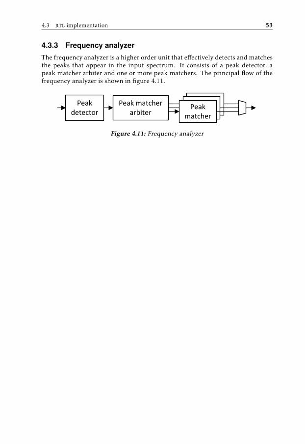
4.3.3 Frequency analyzer
The frequency analyzer is a higher order unit that effectively detects and matchesthe peaks that appear in the input spectrum. It consists of a peak detector, apeak matcher arbiter and one or more peak matchers. The principal flow of thefrequency analyzer is shown in figure 4.11.
Peak matcher arbiter
Peak detector
Peak matcher
Figure 4.11: Frequency analyzer
54 4 Frequency analysis and the dsp
Peak detector
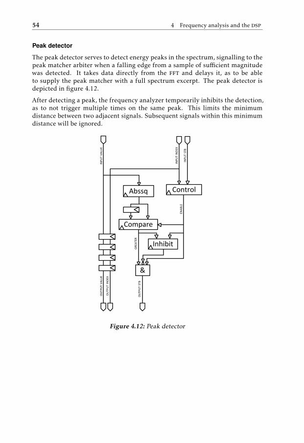
The peak detector serves to detect energy peaks in the spectrum, signalling to thepeak matcher arbiter when a falling edge from a sample of sufficient magnitudewas detected. It takes data directly from the fft and delays it, as to be ableto supply the peak matcher with a full spectrum excerpt. The peak detector isdepicted in figure 4.12.
After detecting a peak, the frequency analyzer temporarily inhibits the detection,as to not trigger multiple times on the same peak. This limits the minimumdistance between two adjacent signals. Subsequent signals within this minimumdistance will be ignored.
Abssq Control
INP
UT
VA
LUE
INP
UT
IND
EX
GR
EATE
R
INP
UT
STB
Compare
&
ENA
BLE
Inhibit
OU
TPU
T V
ALU
E
OU
TPU
T IN
DEX
OU
TPU
T ST
B
Figure 4.12: Peak detector

4.3 rtl implementation 55
Peak matcher arbiter
The peak matcher arbiter’s main role is to distribute the workload among the freepeak matchers. The principal schematic is depicted in figure 4.13.
The peak matchers that follow the arbiter can only receive one spectrum excerptat a time, which prevents peaks with overlapping spectrums to be detected bythe same peak matcher. The peak matcher arbiter serves the spectrum excerptonly to a peak matcher that is free to receive more input.
Each peak matcher comes with a multiply-and-accumulate pipeline, and increas-ing the number of peak matchers improves performance. This effectively de-creases the latency of the algorithm when encountering multiple peaks.
STB 1
STB 2
FREE 1
FREE 2STB
VALUE
INDEX
STB N FREE N
...
Peak matcher 2N-to-M encoder
Peak matcher 1
Peak matcher N
Figure 4.13: Peak matcher arbiter
Peak matcher
Each peak matcher unit consists of a complex multiply-and-accumulate (mac)pipeline that computes the correlation between the samples and the Hammingwindow in the frequency domain at a certain offset. The peak matcher is depictedin figure 4.14.
At the end of the mac pipeline is a magnitude unit that calculates the square ofthe magnitude, |z|2 = <{z}2 +={z}2. In this implementation the square of themagnitude is used instead of just the magnitude since taking the square root isexpensive in hardware, and not needed since the maximum will be found just aswell using this metric.
The pipeline is controlled by a number of state machines implementing heuristicsto maximize the magnitude squared |z|2, i.e. finding the peak.
To maximize pipeline utilization the unit can process more than one peak simul-taneously, time-sharing the mac unit between them.

56 4 Frequency analysis and the dsp
CO
RR S
TB
PR
OG
RES
S
CO
RR S
LOT
Peak arbiter
Correlator search
STB
END
FIR
ST
SLO
T
PO
S
Subsample index
CORR POSC
OR
R A
CK
Dispatcher
CLE
AR
MAC
SAMPLE ADDRSample memory
Window table
WINDOW ADDR
SAMPLE DATA
WINDOW DATA
AC
K
Record keeper
FIR
ST
SLO
T
CO
MM
AN
D V
ALI
D
CO
RR E
ND
GREATER
Complex value
Magnitude
SEA
RC
H E
ND
PO
S
OUTPUT STB
OUTPUT ACK
OU
TPU
T SL
OT
OU
TPU
T SU
BSA
MP
LE IN
DEX
Sample index Calc freq
OUTPUT SAMPLE INDEXOUTPUT FREQ
INPUT VALUE
Sample shifter
FREE
SLO
T
FREE
AC
K
INPUT STB
SAM
PLE
AD
DR
OUTPUT VALUE
INPUT INDEX
CO
RR D
ON
E
CO
RR D
ON
E SL
OT
FREE
Figure 4.14: Peak matcher

4.3 rtl implementation 57
4.3.4 Compensator
Following the peak matcher is the compensator unit that compensates for theeffects of the first windowing and the autocorrelation.
It contains two look-up tables containing the normalized reciprocals of the twoeffects, and one complex multiplier taking its factor from one of the tables. Everypeak passes through its pipeline twice to compensate for both effects.
Since the two tables are normalized, the compensation additionally effectivelyscales the peak signature by a coefficient that needs to be compensated for later.For efficiency this scaling is assumed to be performed more efficiently in a laterstage, where the magnitude has been obtained and doesn’t require a complexmultiplication.
4.3.5 Results
The vhdl model was simulated in ModelSim, sweeping frequencies over onefrequency bin. The results are shown in figure 4.15, with the two plots depictingthe detected amplitude and detected phase respectively.
50 52 54
0.80
0.85
0.90
0.95
1.00
1.05
1.10
Frequency (MHz)
Am
plitu
de
50 52 54
Frequency (MHz)
Pha
se (
radi
ans)
− π
0
π
Figure 4.15: Detected amplitude and phase
The output shows that the amplitude is determined accurately, but more so atlower frequencies. It shows similar characteristics to the results of the Matlabmodel in figure 4.5.
The phase is detected accurately as well, similar that of the phase detected withthe Matlab model in figure 4.6.

58 4 Frequency analysis and the dsp
The vhdl model achieves satisfactory precision in detecting the important char-acteristics of the interferer.

4.4 Conclusions 59
4.4 Conclusions
Using cross-correlation for the signal detection provides higher frequency, ampli-tude and phase precision. By using a pipelined architecture, multiple signals canbe detected with low latency.
With the acquired results, the dsp fulfills the goals of this work block. Being ableto reliably detect interferers, even those not a multiple of the sampling frequency,is a key feature of the Leon interferer cancellation loop.
This method in tandem with the cascaded fft architecture proves effective in de-tecting close-in interferers. Using a delay line, these interferers can theoreticallybe attenuated by up to 30 dB.
4.4.1 Future work
Since the twiddle factor look-up table and the window look-up table never op-erate simultaneously, they can be merged into one, saving space or complexitydepending on the target hardware.
The radix-4 fft uses a simple finite state machine (fsm) for control, and delaysare manually inserted between the fft stages to prevent data hazards. A thor-ough investigation on the possibilities of reordering the butterfly operations canminimze the required delays between the stages of the fft.
Peak matching is currently done assuming an odd number of samples, and thatthe window function in the frequency domain is truncated outside of N−1
2 fre-quency bins from the center. This makes sense for N = 5, where only the spectralcontents of the main lobe are considered, but for N < 5 precision could be in-creased by not truncating the main lobe contents. This is particularly severe forN = 3, where one of the three samples is currently ignored, losing valuable infor-mation.
4.4.2 Multiple signal detection
Since the signal power outside the main lobe of the Hamming window is low,multiple signals can be distinguished if their main lobes do not overlap. In thiscase, simply discarding the spectral contents of the window outside the main lobewhen correlating still yields good results, and signals can be distinguished if theyare at least five frequency bins apart.
4.4.3 Solving ambiguities
Because of the leakage in the first dft, a blocker detected at a frequency offsetin a specific bin can originate at any frequency fblocker = fof f set + nfs, n ∈ Z, butthen with augmented amplitude and phase.
Introducing diversity by observing the frequency contents in a different bin, orusing a different sampling frequency, a system of linear congruences appear.

60 4 Frequency analysis and the dsp
With enough observations with orthogonal parameters, all blockers can be dis-tinguished.
Traditional algorithms for solving systems of linear congruences will not sufficesince the detected values are not well-known integers. Instead, a system follow-ing the fuzzy math discipline is more likely to succeed, implementing an algo-rithm for solving a system of fuzzy linear congruences. This is beyond the scopeof this document.

5Summary
The task of this thesis was divided into two parts. The first task was to inves-tigate the signal processing aspects of the Leon loop, develop a Matlab modeland finally write an rtl model in vhdl. The second task was to continue thedevelopment of the sasp and advance it towards its tape-out.
Development of the sasp yielded new control and data structures, increasing thereliability and speed of the circuit. The weighting unit, responsible for perform-ing the multiplications in the fft algorithm, was improved and its linearity issueswere alleviated. The gains were verified via simulations with extracted parasitics.
The dsp was modeled in Matlab and an algorithm for fine peak detection wasdeveloped. This method, using correlation, was implemented in vhdl along witha radix-4 fft implementation.
5.1 Conclusions
More detailed conclusions can be found in the respective sections of the two workitems; section 3.5 for the sasp and section 4.4 for the dsp.
At the end of the thesis, the work on the sasp had come a long way. Improvingthe linearity, power consumption and speed has been a priority as it is essentialfor the overall functionality of the feedback system proposed in the Leon project.
The blocks that were worked on, including the address generator, rom structuresand weighting unit are shown to work well in simulations, and reach their stipu-lated design goals.
The work on the dsp ended with a full vhdl model, including a full fft im-
61

62 5 Summary
plementation constructed with synthesis on an fpga in mind. It uses cross-correlation to increase the precision of the signal detection, a method that workswell in simulations.
Using the original premise of the Leon project; a cascaded fft configuration to-gether with the improved signal detection yields good results and interferers cantheoretically be attenuated by up to 30 dB.
5.2 Future work
More detailed discussions on future work can be found in the respective sectionsof the two work items; section 3.5.1 for the sasp and section 4.4.1 for the dsp.
There still remained work on the sasp at the end of this thesis. The work is to beresumed and finished and the chip will then finally be sent to fabrication.
As for the dsp, it needs to be implemented in a specific fpga architecture. Somemodern logic synthesizers have the capability of inferring hardware blocks suchas memories and multipliers, but some degree of architecture-specific optimiza-tion is inevitable. After porting, the true performance of the dsp will show.
The sasp and the dsp will need to be tested together to see the open-loop perfor-mance of the interferer detection algorithm with real signals.
Finally the entire, closed loop of project Leon needs to be simulated in its entirety.The signal generator, the delay line and the signal combiner needs to be presentat this stage. When this is done the true capabilities of the project will show.
5.3 Final words
The work on the sasp and the dsp carried widely different requirements andapproaches.
The sasp had a clear goal from the start and its iterative process had alreadybegun when the work was resumed. The work done in this thesis on the saspmoved it towards its completion.
The work on the dsp was more open and encouraged innovation. This allowedtime for reflection and research, and allowed for the discovery of using cross-correlation. This method overcame the principal limitation of the dsp, namelythe ability to accurately identify interferers at frequencies other than multiplesof the sampling frequency.
The dsp finally had a viable rtl model for synthesis on an fpga. Simulationsshow promising results.
This thesis has enabled me to explore two widely different domains of engineer-ing, and I have learned a great deal on how to solve engineering problems in thetwo.

5.3 Final words 63
I am confident that project Leon will play a significant role in the future of soft-ware radio as it elegantly solves one of its fundamental problems with interferers.

Bibliography
Y. Abiven. A low-power 2 GHz discrete time weighting system dedicated to sam-pled analog signal processing. ICECS, pages 57–60, 2011. Cited on page 29.
J. W. Cooley and J. W. Tukey. An algorithm for the machine calculation of com-plex fourier series. Math. Comput., 19:297–301, 1965. Cited on pages 17 and 27.
Y. Deval. Low cost mobile RF terminal paradigms: From multi-radio to softwareradio. In IEEE International Conference on Solid-State and Integrated Circuit Tech-nology (ICSICT), pages 627–630, 2010. Cited on page 22.
M. Kitsunezuka, K. Kunihiro, and M. Fukaishi. Efficient use of the spectrum.IEEE Microwave Magazine, 13(1):55–63, Jan/Feb 2012. Cited on page 22.
P. Kogge and H. Stone. A parallel algorithm for the efficient solution of a generalclass of recurrence equations. IEEE Transactions on Computers, pages 783–791,1973. Cited on page 31.
J. Mitola III. The software radio architecture. IEEE Transactions on Computers, 33:26–38, May 1995. Cited on page 22.
J. Mitola III and G. Q. Maguire, Jr. Cognitive radio: Making software radios morepersonal. IEEE Pers. Commun, 6(4):13–18, Aug 1999. Cited on page 22.
B. Razavi. Cognitive radio design challenges and techniques. IEEE J. Solid-StateCircuits, 45(8):1542–1553, Aug 2010. Cited on page 22.
François Rivet. Design of a Radio Frequency Front-End Receiver dedicated toSoftware-Radio for Mobile Terminals. PhD thesis, University of Bordeaux 1, 2009.Cited on pages 18 and 27.
J. Yuan and C. Svensson. High-speed CMOS circuit technique. IEEE J. Solid-StateCircuits, 24(1):62–70, Feb 1989. Cited on page 31.
65


ASignal detection with
cross-correlation
To properly identify the frequency, magnitude and phase of sinusoidal blockers,the distortion introduced by windowing needs to be countered.
A real sinusoidal input signal can be rewritten as two complex ones.
Sin(t) = Ain cos(ϕin + 2πfint)
= Ainexp(i(ϕin + 2πfint)) + exp(−i(ϕin + 2πfint))
2
(A.1)
Observing only the positive frequency of the real signal, it can be rewritten as
Sin,pos(t) =Ain2
exp(i(ϕin + 2πfint)) (A.2)
The windowing of the input signal yields a convolution with said window in thefrequency domain. Since the main lobe of the Hamming window extends overseveral frequency bins, leakage into adjacent frequency bins is significant. Forthis reason, when observing spectral components in a bin, the actual frequencyof the originating signal is ambiguous.
Furthermore, the Hamming window contains frequency components extendingtowards infinity, and this in combination with sampling leads to aliasing. Thisis usually not a problem, unless the signal frequency is in the first or last fre-quency bins, where leakage of the main lobe of the signal’s negative frequencycounterpart creates an alias of equal magnitude in the very same bin.
Treating the effects of aliasing separately, the contribution from Sin,pos to a fre-
67

68 A Signal detection with cross-correlation
quency bin n in a dft started at a time kTDFT , k ∈ Z can be regarded as
Bin,pos[n] = AHamming (nfs − fin)Ain2
exp(i(ϕin + 2πfinkTDFT )) (A.3)
Introducing the variable fof f set = nfs − fin, Bin,pos[n] can be rewritten as
Bin,pos[n] =AHamming (fof f set)Ain2
exp(i(ϕin + 2π(fof f set + nfs)kTDFT ))
=AHamming (fof f set)Ain2
exp(i(ϕin + 2πfof f setkTDFT )) exp(i(2πnfskTDFT ))
(A.4)
Observing that the time between successive runs of the first dft of N samples isTDFT = N/fs, the last factor resolves to unity;
exp(i(2πnfskTDFT )) = exp(i(2πnfskNfs
)) = exp(i(2πnkN )) = 1 (A.5)
Sampling the output of bin n over successive runs of the first dft, with k =0, 1, 2, 3, . . . , K − 1, the signal will appear as a complex sinusoidal with frequencyfof f set . Performing a second dft on this sequence of samples will yield the con-tribution to frequency bin m;
Bin,pos[n, m] =AHamming (mfDFT − fof f set)
AHamming (fof f set)Ain2
exp(iϕin)(A.6)
With sufficiently large K , the frequency offset within the bin of the first dft,fof f set , can be acquired with some precision, and the effects of the first Ham-ming window can be countered. However, the effects of the second Hammingwindow still cause problems when determining the amplitude and phase of theblocker, since even a small offset in frequency will cause distortion as per fig-ures 4.3 and 4.4.
This problem can be facilitated with using cross-correlation on the output of thesecond dft with a fine-grained Hamming window in the frequency domain. Thepeak of the complex cross-correlation will yield the most likely frequency of theblocker.
(AHamming ? Bin,pos)(f ) =∑m
(A∗Hamming (mfDFT + f )AHamming (mfDFT − fof f set)
AHamming (fof f set)Ain2
exp(iϕin)) (A.7)

69
● ● ● ● ●
●
●
●●
●
● ● ● ● ● ●
−5 0 5
Frequency bin
Mag
nitu
de
Figure A.1: Precise signal frequency implied by correlating with the window
Relating to previous discussions, a sinusoidal signal at the input of the seconddft will appear in the frequency spectrum as a Hamming window.
The peak of the cross-correlation between the dft output and the Hamming win-dow appear where the input likely originated.
Since the Hamming window is heavily attenuated outside of the main lobe, pe-ripheral frequencies can be ignored, trading the accuracy loss for computationalefficiency. When limiting the frequency band, and also assuming that all spectralcomponents are spaced by at least the same frequency offset, the cross-correlationcan be regarded as a shifted version of the Hamming window’s autocorrelationfunction.
This operation becomes an instance of autocorrelation. A property of autocorrela-tion is that its maximum value is found at a lag of zero; in this case at f = −fof f set .Detecting this peak yields fof f set . The value of the autocorrelation is then;
ACorr (f ) =∑m
(A∗Hamming (mfDFT − f )
AHamming (mfDFT − f ))
=∑m
|AHamming (mfDFT − f )|2
(A.8)

70 A Signal detection with cross-correlation
This function is periodic with fDFT , and its effects can be countered when fof f setis known, as is the case after the peak detection.
Having detected a peak at f with (AHamming ? Bin,pos)(f ), and removed window-ing artifacts by dividing by ACorr (f ) and AHamming (f ), and then multiplying bytwo, the original signal amplitude and phase is obtained.
Ain exp(iϕin) (A.9)
BFast Fourier transform
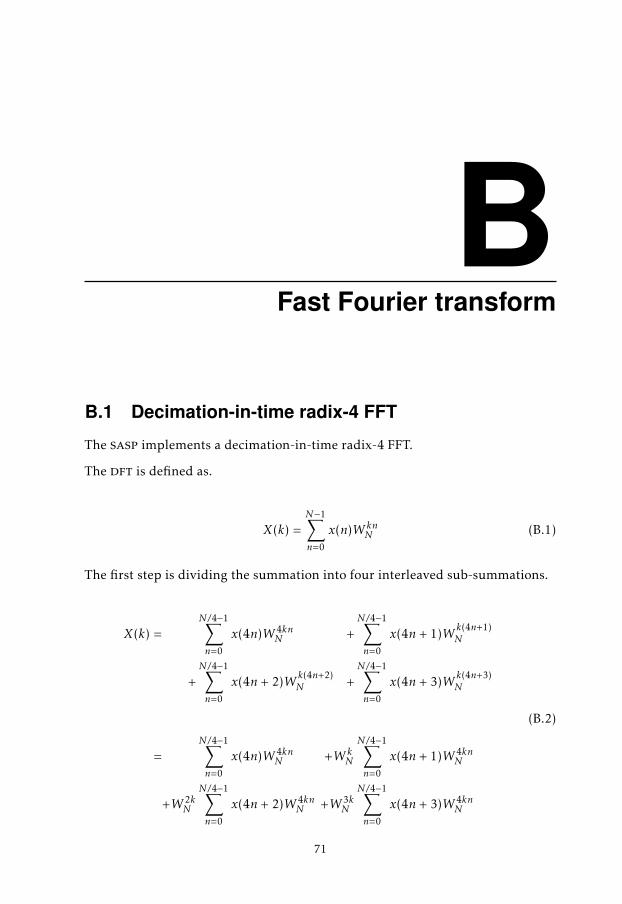
B.1 Decimation-in-time radix-4 FFT
The sasp implements a decimation-in-time radix-4 FFT.
The dft is defined as.
X(k) =N−1∑n=0
x(n)W knN (B.1)
The first step is dividing the summation into four interleaved sub-summations.
X(k) =N/4−1∑n=0
x(4n)W 4knN +
N/4−1∑n=0
x(4n + 1)W k(4n+1)N
+N/4−1∑n=0
x(4n + 2)W k(4n+2)N +
N/4−1∑n=0
x(4n + 3)W k(4n+3)N
=N/4−1∑n=0
x(4n)W 4knN +W k
N
N/4−1∑n=0
x(4n + 1)W 4knN
+W 2kN
N/4−1∑n=0
x(4n + 2)W 4knN +W 3k
N
N/4−1∑n=0
x(4n + 3)W 4knN
(B.2)
71

72 B Fast Fourier transform
Now the recursive nature of the decomposition starts to show, as the four sum-mations are in themselves the very definitions of smaller dft instances. The foursummations are defined as follows, for i = 0, 1, 2, 3.
Fi(k) =N/4−1∑n=0
x(4n + i)W 4knN
=N/4−1∑n=0
x(4n + i)W knN/4
(B.3)
An interesting property of this definition is that W 4knN is cyclic with a period
of N4 . This means that Fi(k) = Fi(k + N
4 ) = Fi(k + N2 ) = Fi(k + 3N
4 ), i.e. fouroutput samples share the same recursivedft. Aligning these four output samplesillustrates the benefit of this.
X (k) = F0(k) +W kNF1(k)
+W 2kN F2(k) +W 3k
N F3(k)
X(k +
N4
)= F0(k + N/4) +W k+N/4
N F1(k + N/4)
+W 2(k+N/4)N F2(k + N/4) +W 3(k+N/4)
N F3(k + N/4)
X(k +
N2
)= F0(k + N/2) +W k+N/2
N F1(k + N/2)
+W 2(k+N/2)N F2(k + N/2) +W 3(k+N/2)
N F3(k + N/2)
X(k +
3N4
)= F0(k + 3N/4) +W k+3N/4
N F1(k + 3N/4)
+W 2(k+3N/4)N F2(k + 3N/4) +W 3(k+3N/4)
N F3(k + 3N/4)
(B.4)
Using the identity discussed above, and simplifying the twiddle factors;

B.1 Decimation-in-time radix-4 FFT 73
X (k) = F0(k) +W kNF1(k) +W 2k
N F2(k) +W 3kN F3(k)
X(k +
N4
)= F0(k) −jW k
NF1(k) −W 2kN F2(k) +jW 3k
N F3(k)
X(k +
N2
)= F0(k) −W k
NF1(k) +W 2kN F2(k) −W 3k
N F3(k)
X(k +
3N4
)= F0(k) +jW k
NF1(k) −1W 2kN F2(k) +jW 3k
N F3(k)
(B.5)
In matrix form;
X (k)
X(k + N
4
)X
(k + N
2
)X
(k + 3N
4
) =
1 1 1 11 −j −1 j
1 −1 1 −11 j −1 −j
1
W kN
W 2kN
W 3kN
ᵀ F0(k)F1(k)F2(k)F3(k)
ᵀ
(B.6)
It is possible to further reduce the number of additions through decomposing thesquare matrix, producing the final expression for the radix-4 decimation-in-timedecomposition butterfly.
X(k)
X(k + N4 )
X(k + N2 )
X(k + 3N4 )
=
1 0 1 00 1 0 −j1 0 −1 00 1 0 j
1 0 1 01 0 −1 00 1 0 10 1 0 −1
1
W kN
W 2kN
W 3kN
ᵀ F0(k)F1(k)F2(k)F3(k)
ᵀ
(B.7)
To illustrate the flow of data when applying the decimation-in-time algorithmrecursively, a butterfly operation is abstracted to its graph form in Figure B.1.Figure B.2 shows the full flow graph for a 64-point radix-4 decimation-in-timeFFT. Note that the direction of the flow is from left to right.
F0(k)
F1(k)
F2(k)
F3(k)
X(k)
X(k + N/4)
X(k + N/2)
X(k + 3N/4)
Figure B.1: FFT radix-4 decimation-in-time butterfly

74 B Fast Fourier transform
x(0)x(16)x(32)x(48)x(4)x(20)x(36)x(52)x(8)x(24)x(40)x(56)x(12)x(28)x(44)x(60)x(1)x(17)x(33)x(49)x(5)x(21)x(37)x(53)x(9)x(25)x(41)x(57)x(13)x(29)x(45)x(61)x(2)x(18)x(34)x(50)x(6)x(22)x(38)x(54)x(10)x(26)x(42)x(58)x(14)x(30)x(46)x(62)x(3)x(19)x(35)x(51)x(7)x(23)x(39)x(55)x(11)x(27)x(43)x(59)x(15)x(31)x(47)x(63)
X(0)X(1)X(2)X(3)X(4)X(5)X(6)X(7)X(8)X(9)X(10)X(11)X(12)X(13)X(14)X(15)X(16)X(17)X(18)X(19)X(20)X(21)X(22)X(23)X(24)X(25)X(26)X(27)X(28)X(29)X(30)X(31)X(32)X(33)X(34)X(35)X(36)X(37)X(38)X(39)X(40)X(41)X(42)X(43)X(44)X(45)X(46)X(47)X(48)X(49)X(50)X(51)X(52)X(53)X(54)X(55)X(56)X(57)X(58)X(59)X(60)X(61)X(62)X(63)
Figure B.2: 64-point FFT radix-4 decimation-in-time diagram

B.2 Decimation-in-frequency radix-4 FFT 75
B.2 Decimation-in-frequency radix-4 FFT
The rtl implementation uses a decimation-in-frequency radix-4 FFT architec-ture.
The dft is defined as.
X(k) =N−1∑n=0
x(n)W knN = dft
{x(n)
}(k) (B.8)
The first step is dividing the summation into four consecutive sub-summations.
X(k) =N/4−1∑n=0
x(n)W knN +
N/4−1∑n=0
x(n+N/4)Wk(n+N/4)N
+N/4−1∑n=0
x(n+N/2)Wk(n+N/2)N +
N/4−1∑n=0
x(n+3N/4)Wk(n+3N/4)N
=N/4−1∑n=0
x(n)W knN +W kN/4
N
N/4−1∑n=0
x(n+N/4)W knN
+W kN/2N
N/4−1∑n=0
x(n+N/2)W knN +W 3kN/4
N
N/4−1∑n=0
x(n+3N/4)W knN
=N/4−1∑n=0
[x(n) + (−j)kx(n+N/4) + (−1)kx(n+N/2) + jkx(n+3N/4)
]W knN
(B.9)
As in the case with the decimation-in-time decomposition, another dft starts toshow. To enable a recursive definition, the output samples are interleaved in fourparts.

76 B Fast Fourier transform
X(4k) =N/4−1∑n=0
[x(n) + (−j)4kx(n+N/4) + (−1)4kx(n+N/2) + j4kx(n+3N/4)
]W knN
X(4k+1) =N/4−1∑n=0
[x(n) + (−j)4k+1x(n+N/4) + (−1)4k+1x(n+N/2) + j4k+1x(n+3N/4)
]W
(4k+1)nN
X(4k+2) =N/4−1∑n=0
[x(n) + (−j)4k+2x(n+N/4) + (−1)4k+2x(n+N/2) + j4k+2x(n+3N/4)
]W
(4k+2)nN
X(4k+3) =N/4−1∑n=0
[x(n) + (−j)4k+3x(n+N/4) + (−1)4k+3x(n+N/2) + j4k+3x(n+3N/4)
]W
(4k+3)nN
(B.10)
Using rules for the twiddle factors, the four equations can be simplified.
X(4k) =N/4−1∑n=0
[x(n) + x(n+N/4) + x(n+N/2) + x(n+3N/4)
]W knN/4
X(4k+1) =N/4−1∑n=0
[x(n) − jx(n+N/4) − x(n+N/2) + jx(n+3N/4)
]W nNW
knN/4
X(4k+2) =N/4−1∑n=0
[x(n) − x(n+N/4) + x(n+N/2) − x(n+3N/4)
]W 2nN W kn
N/4
X(4k+3) =N/4−1∑n=0
[x(n) + jx(n+N/4) − x(n+N/2) − jx(n+3N/4)
]W 3nN W kn
N/4
(B.11)
Now four smaller instances of the dft definition appear.
X(4k) =dft{x(n) +x(n+N/4) +x(n+N/2) +x(n+3N/4)
}(k)
X(4k+1) =dft{[x(n) −jx(n+N/4) −x(n+N/2) +jx(n+3N/4)
]W nN
}(k)
X(4k+2) =dft{[x(n) −x(n+N/4) +x(n+N/2) −x(n+3N/4)
]W 2nN
}(k)
X(4k+3) =dft{[x(n) +jx(n+N/4) −x(n+N/2) −jx(n+3N/4)
]W 3nN
}(k)
(B.12)
The decimation-in-frequency decomposition dispatches four smaller instances ofthe dft algorithm with twiddled inputs. This is in contrast to the decimation-in-time decomposition, which joins the results of four previous instances of the dftalgorithm.

B.2 Decimation-in-frequency radix-4 FFT 77
Indexing the four recursive dft instances i = 0, 1, 2, 3 and letting their respectiveinputs be yi(n), the butterfly of this decomposition can be more readily visualizedin matrix form.
y0(n)y1(n)y2(n)y3(n)
=
1W nN
W 2nN
W 3nN
1 1 1 11 −j −1 j
1 −1 1 −11 j −1 −j
x(n)
x(n+N/4)
x(n+N/2)
x(n+3N/4)
ᵀ
(B.13)
The square matrix for reordering the input samples is identical to the one for thedecimation-in-time decomposition. In fact, the entire butterfly operation onlydiffers by that the decimation-in-time performs the complex rotation at the input,while the decimation-in-frequency case performs it at the output. The reorderingmatrix can be simplified in the same way.
y0(n)y1(n)y2(n)y3(n)
=
1W nN
W 2nN
W 3nN
1 0 1 00 1 0 −j1 0 −1 00 1 0 j
1 0 1 01 0 −1 00 1 0 10 1 0 −1
x(n)
x(n+N/4)
x(n+N/2)
x(n+3N/4)
ᵀ
(B.14)
To illustrate the flow of data when applying the algorithm recursively, a butterflyoperation is abstracted to its graph form in Figure B.3. Figure B.4 shows the fullgraph for a 64-point radix-4 decimation-in-frequency FFT. Note that the direc-tion of the flow is from left to right.
x(n)
x(n + N/4)
x(n + N/2)
x(n + 3N/4)
y0(n)
y1(n)
y2(n)
y3(n)
Figure B.3: FFT radix-4 decimation-in-frequency butterfly
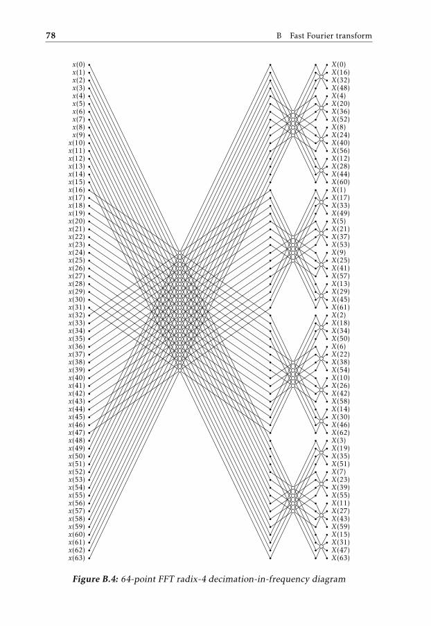
78 B Fast Fourier transform
x(0)x(1)x(2)x(3)x(4)x(5)x(6)x(7)x(8)x(9)x(10)x(11)x(12)x(13)x(14)x(15)x(16)x(17)x(18)x(19)x(20)x(21)x(22)x(23)x(24)x(25)x(26)x(27)x(28)x(29)x(30)x(31)x(32)x(33)x(34)x(35)x(36)x(37)x(38)x(39)x(40)x(41)x(42)x(43)x(44)x(45)x(46)x(47)x(48)x(49)x(50)x(51)x(52)x(53)x(54)x(55)x(56)x(57)x(58)x(59)x(60)x(61)x(62)x(63)
X(0)X(16)X(32)X(48)X(4)X(20)X(36)X(52)X(8)X(24)X(40)X(56)X(12)X(28)X(44)X(60)X(1)X(17)X(33)X(49)X(5)X(21)X(37)X(53)X(9)X(25)X(41)X(57)X(13)X(29)X(45)X(61)X(2)X(18)X(34)X(50)X(6)X(22)X(38)X(54)X(10)X(26)X(42)X(58)X(14)X(30)X(46)X(62)X(3)X(19)X(35)X(51)X(7)X(23)X(39)X(55)X(11)X(27)X(43)X(59)X(15)X(31)X(47)X(63)
Figure B.4: 64-point FFT radix-4 decimation-in-frequency diagram

Upphovsrätt
Detta dokument hålls tillgängligt på Internet — eller dess framtida ersättare —under 25 år från publiceringsdatum under förutsättning att inga extraordinäraomständigheter uppstår.
Tillgång till dokumentet innebär tillstånd för var och en att läsa, ladda ner,skriva ut enstaka kopior för enskilt bruk och att använda det oförändrat för icke-kommersiell forskning och för undervisning. Överföring av upphovsrätten viden senare tidpunkt kan inte upphäva detta tillstånd. All annan användning avdokumentet kräver upphovsmannens medgivande. För att garantera äktheten,säkerheten och tillgängligheten finns det lösningar av teknisk och administrativart.
Upphovsmannens ideella rätt innefattar rätt att bli nämnd som upphovsmani den omfattning som god sed kräver vid användning av dokumentet på ovanbeskrivna sätt samt skydd mot att dokumentet ändras eller presenteras i sådanform eller i sådant sammanhang som är kränkande för upphovsmannens litteräraeller konstnärliga anseende eller egenart.
För ytterligare information om Linköping University Electronic Press se förla-gets hemsida http://www.ep.liu.se/
Copyright
The publishers will keep this document online on the Internet — or its possi-ble replacement — for a period of 25 years from the date of publication barringexceptional circumstances.
The online availability of the document implies a permanent permission foranyone to read, to download, to print out single copies for his/her own use andto use it unchanged for any non-commercial research and educational purpose.Subsequent transfers of copyright cannot revoke this permission. All other usesof the document are conditional on the consent of the copyright owner. Thepublisher has taken technical and administrative measures to assure authenticity,security and accessibility.
According to intellectual property law the author has the right to be men-tioned when his/her work is accessed as described above and to be protectedagainst infringement.
For additional information about the Linköping University Electronic Pressand its procedures for publication and for assurance of document integrity, pleaserefer to its www home page: http://www.ep.liu.se/
© Oskar Holstensson