Embed Size (px)
Citation preview
DATASHEET DS_Q48SD12025_05032012
FEATURES High efficiency: 95.7% @12V/25A
Size:
Without Heat spreader:
58.4mm x 36.8mm x 11.2mm
(2.30”x1.45”x0.44”)
With heat spreader:
58.4mm x 36.8mm x 12.7mm
(2.30”x1.45”x0.50”)
PMBus Rev.1.2 compliance
Industry standard, DOSA compliant pin out
Can be connected in parallel directly
Active current sharing
Fixed frequency operation
Input UVLO, Output OCP & OVP, OTP
Monotonic startup into normal and Pre-biased
loads
2250V Isolation and basic insulation
No minimum load required
ISO 9001, TL 9000, ISO 14001, QS 9000,
OHSAS 18001 certified manufacturing facility
UL/cUL 60950-1 (US & Canada) to be
recognized
APPLICATIONS Telecom / DataCom
Wireless Networks
Optical Network Equipment
Server and Data Storage Industrial/Test Equipment
OPTIONS Digital PMBus interface
Active Current sharing
Trim
Positive On/Off logic
With heatspreader
Short pin lengths available
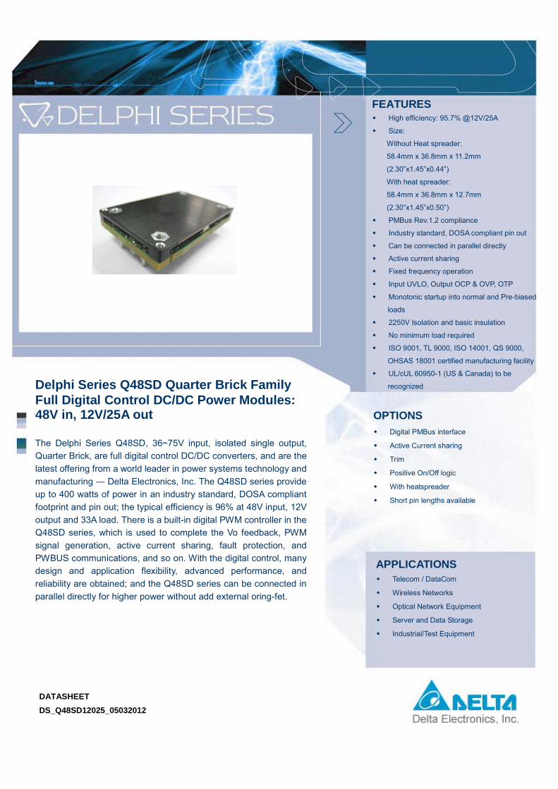
Delphi Series Q48SD Quarter Brick Family Full Digital Control DC/DC Power Modules: 48V in, 12V/25A out The Delphi Series Q48SD, 36~75V input, isolated single output, Quarter Brick, are full digital control DC/DC converters, and are the latest offering from a world leader in power systems technology and manufacturing ― Delta Electronics, Inc. The Q48SD series provide up to 400 watts of power in an industry standard, DOSA compliant footprint and pin out; the typical efficiency is 96% at 48V input, 12V output and 33A load. There is a built-in digital PWM controller in the Q48SD series, which is used to complete the Vo feedback, PWM signal generation, active current sharing, fault protection, and PWBUS communications, and so on. With the digital control, many design and application flexibility, advanced performance, and reliability are obtained; and the Q48SD series can be connected in parallel directly for higher power without add external oring-fet.

DS_Q48SD12025_05032012
2
TECHNICAL SPECIFICATIONS (TA=25°C, airflow rate=300 LFM, Vin=48Vdc, nominal Vout unless otherwise noted.) PARAMETER NOTES and CONDITIONS Q48SD12025 (Standard)
Min. Typ. Max. Units ABSOLUTE MAXIMUM RATINGS Input Voltage
Continuous 80 Vdc Transient (100ms) 100ms 100 Vdc
On/off Pin Voltage -50 50 V
Other Pin Voltage Trim/Current Sharing, C2, Data, SMBAlert, Clock, Addr1Addr0 -0.3 3.6 V
Operating Ambient Temperature -40 85 °C Storage Temperature -55 125 °C Input/Output Isolation Voltage 2250 Vdc INPUT CHARACTERISTICS
Operating Input Voltage 36 75 Vdc Input Under-Voltage Lockout
Turn-On Voltage Threshold 32.5 34 35.5 Vdc Turn-Off Voltage Threshold 30.5 32 33.5 Vdc Lockout Hysteresis Voltage 1 2 3 Vdc
Maximum Input Current Vin=36V, 100% Load, 8.3 8.5 A No-Load Input Current 75 110 mA Off Converter Input Current 18 23 mA Inrush Current(I2t) With 100uF external input capacitor 1 A2s Start up Current Peak, Vin=36V, 100% Load, With 5000uF Co 8.3 12 A Input Terminal Ripple Current RMS, With 100uF input cap. 0.24 0.36 A Input Reflected-Ripple Current P-P thru 12µH inductor, 5Hz to 20MHz 10 mA Input Voltage Ripple Rejection 120 Hz 50 dB
OUTPUT CHARACTERISTICS Output Voltage Set Point Vin=48V, Io=Io.max, Tc=25°C 11.8 12 12.2 Vdc Output Voltage Regulation
Over Load Io=Io,min to Io,max 20 45 mV Over Line Vin=38.5V to 75V 20 45 mV Over Temperature Tc=-40°C to 125°C ±120 mV
Total Output Voltage Range over sample load, and temperature, from 38~75V Vin 11.8 12 12.4 V over sample load, and temperature, from 36~75V Vin 11.2 12 12.4 V Output Voltage Ripple and Noise 5Hz to 20MHz bandwidth
Peak-to-Peak Full Load, 1µF ceramic, 10µF tantalum 100 200 mV RMS Full Load, 1µF ceramic, 10µF tantalum 40 80 mV
Operating Output Current Range Full input voltage range 0 25 A Output DC Current-Limit Inception Output Voltage 10% Low 110 150 %
DYNAMIC CHARACTERISTICS Output Voltage Current Transient 48V, 10µF Tan & 1µF Ceramic load cap, 0.1A/µs
Positive Step Change in Output Current 50% Io.max to 75% Io.max 200 400 mV Negative Step Change in Output Current 75% Io.max to 50% Io.max 200 400 mV Setting Time (within 1% Vout nominal) 300 µs
Turn-On Transient Start-Up Time, From On/Off Control 40 50 ms Start-Up Time, From Input 50 60 ms
Output Capacitance 220 16000 µF EFFICIENCY 100% Load Vin=48V 94.7 95.7% % 60% Load Vin=48V 94.7 95.7% %
ISOLATION CHARACTERISTICS Input to Output 2250 Vdc Isolation Resistance 10 MΩ Isolation Capacitance 1500 pF
FEATURE CHARACTERISTICS Current sharing accuracy 10 % Switching Frequency 130 kHz ON/OFF Control, Negative Remote On/Off logic
Logic Low (Module On) Von/off -0.7 0.8 V Logic High (Module Off) Von/off 2.4 50 V
ON/OFF Control, Positive Remote On/Off logic Logic Low (Module Off) Von/off -0.7 0.8 V Logic High (Module On) Von/off 2.4 50 V
ON/OFF Current (for both remote on/off logic) Ion/off at Von/off=0.0V 0.5 mAON/OFF Current (for both remote on/off logic) Ion/off at Von/off=2.4V 10 µALeakage Current (for both remote on/off logic) Logic High, Von/off=15V 50 µA Output Voltage Trim Range Vin=48V, Pout max rated power≦ -20 10 % Output Over-Voltage Protection Over full temp range; % of nominal Vout 14 17 V
PMBus Signal Interface Characteristics Logic Input Low (VIL) C2, Data, SMBAlert, Clock pin 0 0.8 V Logic Input High (VIH) C2, Data, SMBAlert, Clock pin 2.1 3.3 V Logic Onput Low (VOL) C2, Data, SMBAlert, Clock pin; IOL=6mA 0.4 V Logic Onput High (VOH) C2, Data, SMBAlert, Clock pin; IOH=-6mA 2.6 V PMBus Operating Frequency Range 100 400 KHz

DS_Q48SD12025_05032012
3
TECHNICAL SPECIFICATIONS (TA=25°C, airflow rate=300 LFM, Vin=48Vdc, nominal Vout unless otherwise noted.)
PARAMETER NOTES and CONDITIONS Q48SD12025 (Standard) Min. Typ. Max. Units
PMBus Monitoring CHARACTERISTICS Output Current Reading Accuracy Io=50% ~ 100% of Io, max; -5 +5 % Io=5% ~ 50% of Io, max; -2 +2 A Output Voltage Reading Accuracy -2 +2 % Input Voltage Reading Accuracy -4 +4 % Temperature Reading Accuracy -5 +5
GENERAL SPECIFICATIONS MTBF Io=100% of Io, max; 300LFM; Ta=25°C TBD M hours Weight Without heat spreader 52.5 grams Weight With heat spreader 66.5 grams
Over-Temperature Shutdown ( Without heat spreader) Refer to Figure 22 for Hot spot 1 location (48Vin,80% Io, 200LFM,Airflow from Vin+ to Vin-) 128 °C
Over-Temperature Shutdown (With heat spreader) Refer to Figure 24 for Hot spot 2 location (48Vin,80% Io, 200LFM,Airflow from Vin+ to Vin-) 120 °C
Over-Temperature Shutdown ( NTC resistor ) Refer to Figure 22 for NTC resistor location 125 °C Note: Please attach thermocouple on NTC resistor to test OTP function, the hot spots’ temperature is just for reference.
PIN DEFINATION Pin# Name Function Pin# Name Function
1 Vin(+) 7 C2 Secondary on/off control pin; The default configuration is set to ignore this
input. And such pin can be reconfigured by the PMBus Interface.
2 ON/OFF Primary on/off control pin 8 Sig_Gnd Signal ground
3 Vin(-) 9 Data PMBus data line
4 Vo(-) 10 SMBAlert PMBus SMBAlert line
5 Trim
/Current sharing
Trim pin or current sharing pin,
which is option. 11 Clock PMBus clock line
6 Vo(+) 12 Addr1 ADDR1 pin sets the high order digit of the address.
13 Addr0 ADDR0 pin sets the low order digit of the address.
SIMPLIFIED APPLICATION CIRCUIT
Vout(+)
Trim/Current sharing
Addr0 Addr1
Vout(-)
Vin(+)
Vin(-)
On/off
Delta DC/DC Module
EMI filter
Reverse polarity
Protection
Fuse
LoadInput Source
System MCU
CLOCK DATA C2SMB
-ALERT
CLK DATA CTRLALERT
On/off control
Vout(+)
Trim/Current sharing
Addr0 Addr1
Vout(-)
Vin(+)
Vin(-)
On/off
Delta DC/DC Module
EMI filter
Reverse polarity
Protection
Fuse
LoadInput Source
System MCU
CLOCK DATA C2SMB
-ALERT
CLK DATA CTRLALERT
On/off control

DS_Q48SD12025_05032012
4
ELECTRICAL CHARACTERISTICS CURVES
80
84
88
92
96
100
2.5 5 7.5 10 12.5 15 17.5 20 22.5 25
Output Current (A)
Effi
cien
cy (%
)
75V 48V 36V
0
4
8
12
16
2.5 5 7.5 10 12.5 15 17.5 20 22.5 25
Output Current (A)P
ower
Los
s (W
)75V 48V 36V
Figure 1: Efficiency vs. load current for minimum, nominal, and maximum input voltage at 25°C
Figure 2: Power dissipation vs. load current for minimum, nominal, and maximum input voltage at 25°C
0
4
8
12
16
0 12.5 25 33 40
Output Current (A)
Out
put V
olta
ge (V
)
Figure 3: Typical full load input characteristics at room temperature
Figure 4: Output voltage regulation vs load current showing typical current limit curves and converter shutdown points for minimum, nominal, and maximum input voltage at room temperature

DS_Q48SD12025_05032012
5
ELECTRICAL CHARACTERISTICS CURVES For Negative Remote On/Off Logic
Figure 5: Turn-on transient at zero load current (10ms/div).Vin=48V. Top Trace: Vout, 5V/div; Bottom Trace: ON/OFF input,2V/div
Figure 6: Turn-on transient at full rated load current (constant current load) (10 ms/div). Vin=48V. Top Trace: Vout, 5V/div; Bottom Trace: ON/OFF input, 2V/div
For Input Voltage Start up
Figure 7: Turn-on transient at zero load current (10 ms/div).Vin=48V. Top Trace: Vout, 5V/div, Bottom Trace: input voltage,30V/div
Figure 8: Turn-on transient at full rated load current (constant current load) (10 ms/div). Vin=48V. Top Trace: Vout, 5V/div; Bottom Trace: input voltage, 30V/div

DS_Q48SD12025_05032012
6
ELECTRICAL CHARACTERISTICS CURVES
Figure 9: Output voltage response to step-change in load current (75%-50% of Io, max; di/dt = 0.1A/µs, Vin=48V). Load cap: 10µF, tantalum capacitor and 1µF ceramic capacitor. Top Trace: Vout (200mV/div, 200us/div); Bottom Trace: Io (12A/div, 200us/div). Scope measurement should be made using a BNC cable (length shorter than 20 inches). Position the load between 51 mm to 76 mm (2 inches to 3 inches) from the module..
Figure 10: Output voltage response to step-change in load current (50%-75% of Io, max; di/dt = 0.1A/µs, Vin=48V). Load cap: 10µF, tantalum capacitor and 1µF ceramic capacitor. Top Trace: Vout (200mV/div, 200us/div); Bottom Trace: Io (12A/div, 200us/div). Scope measurement should be made using a BNC cable (length shorter than 20 inches). Position the load between 51 mm to 76 mm (2 inches to 3 inches) from the module..
Figure 11: Test set-up diagram showing measurement points for Input Terminal Ripple Current and Input Reflected Ripple Current. Note: Measured input reflected-ripple current with a simulated source Inductance (LTEST) of 12 µH. Capacitor Cs offset possible battery impedance. Measure current as shown below
Figure 12: Input Terminal Ripple Current, ic, at full rated output current and nominal input voltage with 12µH source impedance and 100µF electrolytic capacitor (75 mA/div, 2us/div).
Vin+
Vin-
is ic
100uF,
ESR=0.2 ohm @ 25oC 100KHz
Cs: 220uF
+ +
Vin+
Vin-
is ic
100uF,
ESR=0.2 ohm @ 25oC 100KHz
Cs: 220uF
+ +
is ic
100uF,
ESR=0.2 ohm @ 25oC 100KHz
Cs: 220uF
++ ++

DS_Q48SD12025_05032012
7
ELECTRICAL CHARACTERISTICS CURVES
Vo(-)
Vo(+)
10u 1u
Copper Strip
SCOPE RESISTIVELOAD
Figure 13: Input reflected ripple current, is, through a 12µH source inductor at nominal input voltage and rated load current (20 mA/div, 5us/div).
Figure 14: Output voltage noise and ripple measurement test setup
Figure 15: Output voltage ripple at nominal input voltage and rated load current (Io=33A)(50 mV/div, 2us/div) Load capacitance: 1µF ceramic capacitor and 10µF tantalum capacitor. Bandwidth: 20 MHz. Scope measurements should be made using a BNC cable (length shorter than 20 inches). Position the load between 51 mm to 76 mm (2 inches to 3 inches) from the module.

DS_Q48SD12025_05032012
8
Safety Considerations The power module must be installed in compliance with the spacing and separation requirements of the end-user’s safety agency standard, i.e., UL60950-1, CSA C22.2 NO. 60950-1 2nd, IEC 60950-1 2nd : 2005, EN 60950-1 2nd: 2006+A11+A1: 2010, if the system in which the power module is to be used must meet safety agency requirements. Basic insulation based on 75 Vdc input is provided between the input and output of the module for the purpose of applying insulation requirements when the input to this DC-to-DC converter is identified as TNV-2 or SELV. An additional evaluation is needed if the source is other than TNV-2 or SELV. When the input source is SELV circuit, the power module meets SELV (safety extra-low voltage) requirements. If the input source is a hazardous voltage which is greater than 60 Vdc and less than or equal to 75 Vdc, for the module’s output to meet SELV requirements, all of the following must be met:
The input source must be insulated from the ac mains by reinforced or double insulation.
The input terminals of the module are not operator accessible.
A SELV reliability test is conducted on the system where the module is used, in combination with the module, to ensure that under a single fault, hazardous voltage does not appear at the module’s output.
When installed into a Class II equipment (without grounding), spacing consideration should be given to the end-use installation, as the spacing between the module and mounting surface have not been evaluated. The power module has extra-low voltage (ELV) outputs when all inputs are ELV. This power module is not internally fused. To achieve optimum safety and system protection, an input line fuse is highly recommended. The safety agencies require a Fast-acting fuse with 30A maximum rating to be installed in the ungrounded lead. A lower rated fuse can be used based on the maximum inrush transient energy and maximum input current. Soldering and Cleaning Considerations Post solder cleaning is usually the final board assembly process before the board or system undergoes electrical testing. Inadequate cleaning and/or drying may lower the reliability of a power module and severely affect the finished circuit board assembly test. Adequate cleaning and/or drying is especially important for un-encapsulated and/or open frame type power modules. For assistance on appropriate soldering and cleaning procedures, please contact Delta’s technical support team.
DESIGN CONSIDERATIONS Input Source Impedance The impedance of the input source connecting to the DC/DC power modules will interact with the modules and affect the stability. A low ac-impedance input source is recommended. If the source inductance is more than a few µH, we advise adding a 100 to 200 µF electrolytic capacitor (ESR < 0.7 Ω at 100 kHz) mounted close to the input of the module to improve the stability. Layout and EMC Considerations Delta’s DC/DC power modules are designed to operate in a wide variety of systems and applications. For design assistance with EMC compliance and related PWB layout issues, please contact Delta’s technical support team. An external input filter module is available for easier EMC compliance design. Below TBD is the reference design for an input filter tested with Q48SD12025XXXX to meet class B in CISSPR 22.

DS_Q48SD12025_05032012
9
FEATURES DESCRIPTIONS Over-Current Protection The modules include an internal output over-current protection circuit. If the output current exceeds the OCP set point, the modules will shut down, and enter hiccup mode or latch mode. For hiccup mode, the module will try to restart after shutdown. If the overload condition still exists, the module will shut down again. This restart trial will continue until the overload condition is corrected. For latch mode, the module will shut down and not attempt to restart. The latch is reset by either cycling the input power or by toggling the primary on/off signal for one second. The OCP threshold and protection mode can be reconfigured by the PMBus Interface; the default configuration is hiccup mode. Over-Voltage Protection The modules include an internal output over-voltage protection circuit. If output voltage exceeds the over-voltage set point, the module will shut down, and enter in hiccup mode or latch mode. For hiccup mode, the module will try to restart after shutdown. If the output overvoltage condition still exists, the module will shut down again. This restart trial will continue until the over-voltage condition is corrected. For latch mode, the module will shut down and not attempt to restart. The latch is reset by either cycling the input power or by toggling the primary on/off signal for one second. The Vo OVP threshold and protection mode can be reconfigured by the PMBus Interface; The default configuration is hiccup mode. Over-Temperature Protection The modules include an internal over-temperature protection circuit. If the module temperature exceeds the over-temperature threshold the module will shut down, and enter in auto-recovery mode or latch mode. For auto-recovery mode, the module will monitor the module temperature after shutdown. Once the temperature is dropped and within the specification, the module will be auto-recovery. For latch mode, the module will shut down and not attempt to restart. The latch is reset by either cycling the input power or by toggling the primary on/off signal for one second. The OTP threshold and protection mode can be reconfigured by the PMBus Interface; The default configuration is hiccup mode. Primary Remote On/Off The primary remote on/off feature on the module can be either negative or positive logic. Negative logic turns the module on during a logic low and off during a logic high. Positive logic turns the modules on during a logic high and off during a logic low.
The primary remote on/off can be controlled by an external switch between the on/off terminal and the Vi(-) terminal. The switch can be an open collector or open drain. If the remote on/off feature is not used, for negative logic, please short the on/off pin to Vi(-); For positive logic, please leave the on/off pin floating. The module will not response to the remote on/off signal which is less than 120us. The primary remote on/off logic can be reconfigured by the PMBus Interface.
RLoad
Vi(-)
Vi(+)
ON/OFF
Vo(-)
Vo(+)
RLoad
Vi(-)
Vi(+)
ON/OFF
Vo(-)
Vo(+)
Vi(-)
Vi(+)
ON/OFF
Vo(-)
Vo(+)
Figure 17: Remote on/off implementation Secondary Remote On/Off Reference to the Vo(-) terminal, there is a C2 pin. The default configuration is set to ignore this input. And such pin can be reconfigured as secondary remote on/off pin by the PMBus interface including either negative or positive logic. Negative logic turns the module on during a logic low and off during a logic high. Positive logic turns the modules on during a logic high and off during a logic low. The secondary remote on/off can be controlled by an external switch between the on/off terminal and the Vo(-) terminal. The switch can be an open collector or open drain. Parallel and Active Current Sharing The modules are capable of operating in parallel, and realizing current sharing by active current sharing method. The current sharing pin of parallel module are connected together to create a current sharing bus; in this case, so called “Max Current” current sharing bus method is employed. The module with the max output current will be the master module automatically, and it’s output current signal will be sent to the current sharing pin as the current sharing bus signal. The rest module with the lower output current will be the slave module, which will adjust their output voltage in order to bring their output current increasing to the required current by the current sharing bus signal. The current sharing accuracy equation is: X% = | Io – ( Itotal / N ) | / Irated, Where, Io is the output current of per module; Itotal is the total load current; N is parallel module numbers; Irated is the rated full load current of per module.

DS_Q48SD12025_05032012
10
FEATURES DESCRIPTIONS (CON.) If system has no redundancy requirement, the module can be parallel directly for higher power without adding external oring-fet; whereas, If the redundancy function is required, the external oring-fet should be added.
Vin+
Vin-
On/off
Vo+
Vo-
Current Sharing
Module I
Vin+
Vin-
On/off
Vo+
Vo-
Module IICurrent Sharing
Vin Load
Vin+
Vin-
On/off
Vo+
Vo-
Current Sharing
Module I
Vin+
Vin-
On/off
Vo+
Vo-
Module IICurrent Sharing
Vin
Vin+
Vin-
On/off
Vo+
Vo-
Current Sharing
Module I
Vin+
Vin-
On/off
Vo+
Vo-
Module IICurrent Sharing
Vin Load
Figure 18: Parallel and active current sharing configuration for no redundancy requirement system In order to keep the good stability of the parallel system, below layout guideline should be followed: 1. The trace connected the current sharing pin of Module I and Module II should be as short as possible. 2. The layout loop from Module I current sharing pin to Module II current sharing pin, to Module II Vo- pin, and come back to Module I Vo- pin should be as small as possible. 3. The dc voltage drop from Module I Vo- pin to Module II Vo- pin should be as small as possible. PMBus Communication The module has a digital PMBus interface to allow the module to be monitored, controlled and configured by the system. The module supports 4 PMBus signal lines, Data, Clock, SMBALERT (optional), Control (C2 pin, optional), and 2 Address line Addr0 and Addr1. More detail PMBus information can be found in the PMB Power Management Protocol Specification, Part I and part II, revision 1.2; which is shown in http://pmbus.org . Both 100kHz and 400kHz bus speeds are supported by the module. Connection for the PMBus interface should be following the High Power DC specifications given in section 3.1.3 in the SMBus specification V2.0 or the Low Power DC specifications in section 3.1.2. The complete SMBus specification is shown in http://smbus.org. The module supports the Packet Error Checking (PEC) protocol. It can check the PEC byte provided by the PMBus master, and include a PEC byte in all message responses to the master. And the module also can communicate with the master that does not implement the PEC mechanism.
SMBALERT protocol is also supported by the module. SMBALERT line is a wired-AND signal just as the CLOCK and DATA signals; by which the module can alert the PMBus master that it has an active status or alarm condition via pulling the SMBALERT pin to an active low. There are two ways that the master and the module response to the alert o f SMBALERT line. One way is for the module used in a system that does not support ARA. The factory default state for the module is to retain it’s resistor programmed address, when it is in an ALERT active condition, and not respond to the ARA. The master will communicate with the slave module using the programmed address, and using the various READ_STATUS commands to find who cause for the SMBALERT. The CLEAR_FAULTS command will clear the SMBALERT. The other way is for the module used in a system that does support ARA. Bit 4 of the MFR_ARA_CONFIG command can be used to reconfigure the module to utilize Alert Response Address (ARA). In this case, the module will no longer respond to its programmed address. The master simultaneously accesses all SMBALERT devices ARA; only the device which pulled SMBALERT low will acknowledge the ARA. The master is expected to perform the modified received byte operation to get the address of the alert slave, and retire the SMBALERT active signal. And then, the alter slave will return to it’s resistor programmed address, allowing normal master-slave communications to proceed. If more than one device pulls SMBALERT line low, the lowest address device will win communication rights via standard arbitration during the slave address transfer. After acknowledging the slave address the device must disengage its SMBALERT pulldown. If the master still sees SMBALERT line low when the message transfer is complete, it knows to read the ARA again. The module contains a data flash used to store configuration settings, which will not be programmed into the device data flash automatically. The STORE_DEFAULT_ALL command must be used to commit the current settings are transfer from RAM to data flash as device defaults. PMBUS Addressing The Module has flexible PMBUS addressing capability. When connect different resistor from Addr0 and Addr1 pin to GND pin, 64 possible addresses can be acquired. The address is in the form of octal digits; Each pin offer one octal digit, and then combine together to form the decimal address as shown in below. Address = 8 * ADDR1 + ADDR0

DS_Q48SD12025_05032012
11
FEATURES DESCRIPTIONS (CON.)
Corresponded to each octal digit, the requested resistor values are shown in below, and +/-5% resistors accuracy can be accepted. If there is any resistances exceeding the requested range, address 127 will be return. 0-12 and 40, 44, 45, and 55 in decimal address can’t be used, since they are reserved according to the SMBus specifications, and which will also return address 127.
Octal digit Resistor(Kohm)
0 10
1 15.4
2 23.7
3 36.5
4 54.9
5 84.5
6 130
7 200
PMBus Data Format The module receives and report date in LINEAR format. The Exponent of the data words is fixed at a reasonable value for the command; altering the exponent is not supported. DIRECT format is not supported by the module. For commands that set or report any voltage thresholds related to the output voltage, the module supports the linear data format consisting of a two byte value with a 16-bit, unsigned mantissa, and a fixed exponent of -12. The format of the two data bytes is shown below:
The equation can be written as: Vout = Mantissa x 2-12 For example, considering set Vout to 12V by VOUT_COMMAND, the read/write data can be calculated refer to below process: 1. Mantissa =Vout/2-12= 12/2-12=49152; 2. Converter the calculated Mantissa to hexadecimal
0xC000. For commands that set or report all other thresholds, including input voltages, output current, temperature, time and frequency, the supported linear data format is a two byte value with: an 11 bit, two’s complement mantissa , and a 5 bit, two’s complement exponent (scaling factor).The format of the two data bytes is shown as in below.
The equation can be written as: Value = Mantissa x 2exponent For example, considering set the turn on threshold of input under voltage lockout to 34V by VIN_ON command; the read/write data can be calculated refer to below process: 1. Get the exponent of Vin, -3; whose binary is 11101 2. Mantissa =Vin/2-3=34/2-3=272; 3. Converter the calculated Mantissa to hexadecimal
110, then converter to binary 00100010000; 4. Combine the exponent and the mantissa, 11101 and
00100010000; 5. Converter binary 1110100100010000 to
hexadecimal E910. The detail exponent and resolution of main parameter is summarized as below:
Exponent Resolution
Vin -3 0.125V
Vo -12 0.244mV
Io -4 62.5mA
Temperature -2 /
Switching requency -2 0.25Khz
Time -1 0.5ms
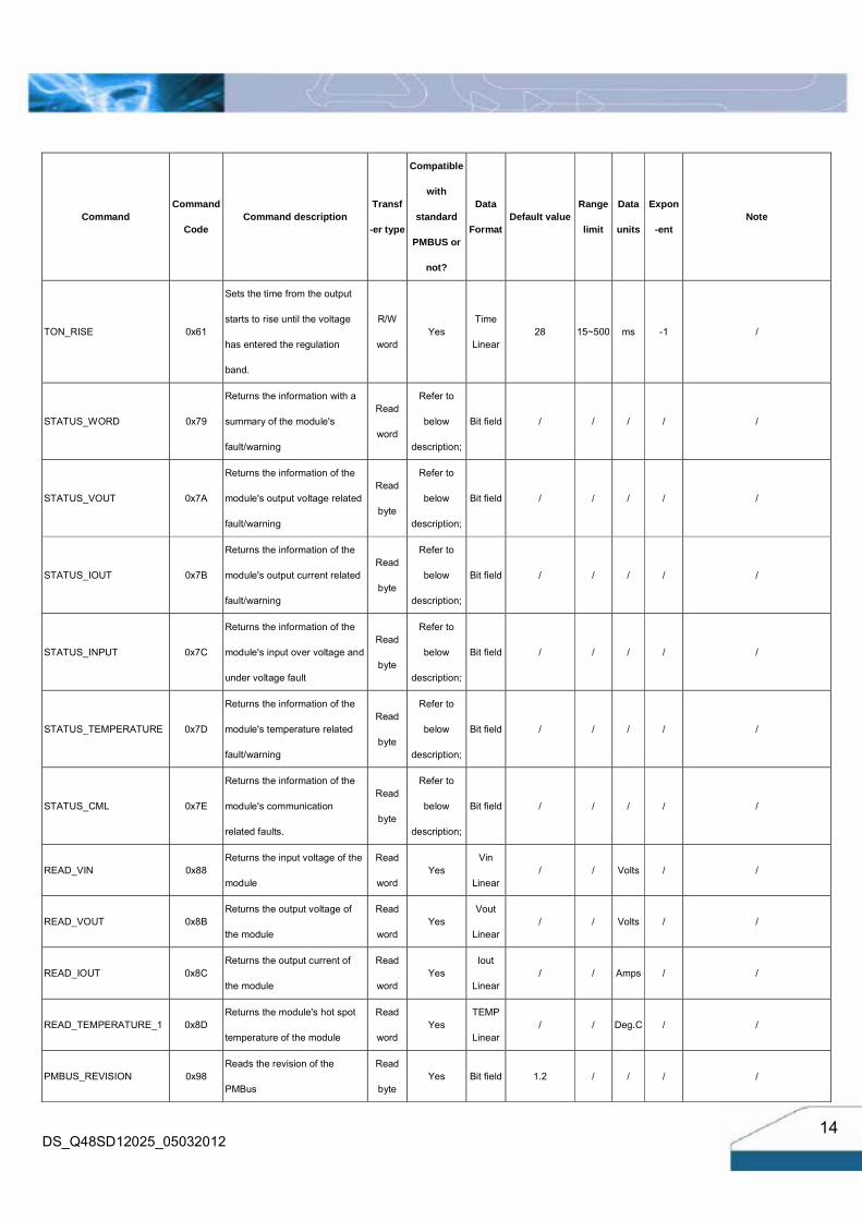
Supported PMBus Commands The main PMBus commands described in the PMBus 1.2 specification are supported by the module. Partial PMBus commands are fully supported; Partial PMBus commands have difference with the definition in PMBus 1.2 specification. All the supported PMBus commands are detail summarized in below table.

DS_Q48SD12025_05032012
12
FEATURES DESCRIPTIONS (CON.)
Command Command
Code Command description
Transf
-er type
Compatible
with
standard
PMBUS or
not?
Data
FormatDefault value
Range
limit
Data
units
Expon
-ent Note
OPERATION 0x01 Turn the module on or off by
PMBUS command
R/W
byte
Refer to
below
description;
Bit field 0x80 / / / /
ON_OFF_CONFIG 0x02
Configures the combination of
primary on/off pin and PMBUS
command
R/W
byte
Refer to
below
description;
Bit field
0x1D
(Neg Logic);
0x1F
(Pos Logic);
/ / / /
CLEAR_FAULTS 0x03 Clear any fault bits that have
been set
Send
byteYes / / / / / /
STORE_DEFAULT_ALL 0x11 Stores operating parameters
from RAM to data flash
Send
byteYes / / / / /
This command is effective to the
parameter of all command in the
table.
RESTORE_DEFAULT_ALL 0x12 Restores operating parameters
from data flash to RAM
Send
byteYes / / / / /
This command can't be issued
when the power unit is running.
VOUT_MODE 0x20 To read Vo data format Read
byteYes
mode+
exp 0x14 / / / /
VOUT_COMMAND 0x21 Set the output voltage R/W
wordYes
Vout
Linear12
9.6
~13.2Volts -12 /
FREQUENCY_SWITCH 0x33 Set the switching frequency R/W
wordYes
Freque
ncy
Linear
130 120
~140KHz -2 /
VIN_ON 0x35
Set the turn on voltage
threshold of Vin under voltage
lockout
R/W
wordYes
Vin
Linear34 32~46 V -3
VIN_ON should be higher than
VIN_OFF, and keep 2V
hystersis.
VIN_OFF 0x36
Set the turn off voltage
threshold of Vin under voltage
lockout
R/W
wordYes
Vin
Linear32 32~46 V -3
VIN_ON should be higher than
VIN_OFF, and keep 2V
hystersis.
VOUT_OV_FAULT_LIMIT 0x40 Set the output overvoltage fault
threshold.
R/W
wordYes
Vout
Linear15 11~16 V -12
Must be higher than the value of
VOUT_COMMAND and
VOUT_OV_WARN_LIMIT;

DS_Q48SD12025_05032012
13
Command Command
Code Command description
Transf
-er type
Compatible
with
standard
PMBUS or
not?
Data
FormatDefault value
Range
limit
Data
units
Expon
-ent Note
VOUT_OV_FAULT_RESP
ONSE 0x41
Instructs what action to take in
response to an output
overvoltage fault.
R/W
byte
Refer to
below
description;
Bit field 0xB8 / N/A / /
VOUT_OV_WARN_LIMIT 0x42 Set a threshold causing an
output voltage high warning.
R/W
wordYes
Vout
Linear15 11~16 V -12
Must be less than
VOUT_OV_FAULT_LIMIT value
IOUT_OC_FAULT_LIMIT 0x46 Set the output overcurrent fault
threshold.
R/W
wordYes
Iout
Linear33 20~60 A -4
Must be greater than
IOUT_OC_WARN_LIMIT value
IOUT_OC_FAULT_RESPO
NSE 0x47
Instructs what action to take in
response to an output
overcurrent fault.
R/W
byte
Refer to
below
description;
Bit field 0xF8 / N/A / /
IOUT_OC_WARN_LIMIT 0x4A Set a threshold causing an
output current high warning.
R/W
wordYes
Iout
Linear28 10~40 A -4
Must be less than
IOUT_OC_FAULT_LIMIT value
OT_FAULT_LIMIT 0x4F Set the over temperature fault
threshold.
R/W
wordYes
TEMP
Linear125 25~140 Deg.C -2
Must be greater than
OT_WARN_LIMIT value
OT_FAULT_RESPONSE 0x50
Instructs what action to take in
response to an over
temperature fault.
R/W
byte
Refer to
below
description;
Bit field 0xB8 / N/A / /
OT_WARN_LIMIT 0x51 Set a threshold causing a
temperature high warning.
R/W
wordYes
TEMP
Linear115 25~125 Deg.C -2
Must be less than
OT_FAULT_LIMIT value
VIN_OV_FAULT_LIMIT 0x55 Set the input overvoltage fault
threshold.
R/W
wordYes
Vin
Linear110 48~110 V -3 /
POWER_GOOD_ON 0x5E
Sets the output voltage at which
the bit 3 of STATUS_WORD
high byte should be asserted.
R/W
wordYes
Vout
Linear11
8.1
~13.2V -12
Must be greater than
POWER_GOOD_OFF value by
1.6V
POWER_GOOD_OFF 0x5F
Sets the output voltage at which
the bit 3 of STATUS_WORD
high byte should be negated.
R/W
wordYes
Vout
Linear9
8.1
~13.2V -12
Must be less than
POWER_GOOD_ON value by
1.6V
TON_DELAY 0x60
Sets the time from a start
condition is received until the
output voltage starts to rise
R/W
wordYes
Time
Linear7 5~500 ms -1 /
DS_Q48SD12025_05032012
14
Command Command
Code Command description
Transf
-er type
Compatible
with
standard
PMBUS or
not?
Data
FormatDefault value
Range
limit
Data
units
Expon
-ent Note
TON_RISE 0x61
Sets the time from the output
starts to rise until the voltage
has entered the regulation
band.
R/W
wordYes
Time
Linear28 15~500 ms -1 /
STATUS_WORD 0x79
Returns the information with a
summary of the module's
fault/warning
Read
word
Refer to
below
description;
Bit field / / / / /
STATUS_VOUT 0x7A
Returns the information of the
module's output voltage related
fault/warning
Read
byte
Refer to
below
description;
Bit field / / / / /
STATUS_IOUT 0x7B
Returns the information of the
module's output current related
fault/warning
Read
byte
Refer to
below
description;
Bit field / / / / /
STATUS_INPUT 0x7C
Returns the information of the
module's input over voltage and
under voltage fault
Read
byte
Refer to
below
description;
Bit field / / / / /
STATUS_TEMPERATURE 0x7D
Returns the information of the
module's temperature related
fault/warning
Read
byte
Refer to
below
description;
Bit field / / / / /
STATUS_CML 0x7E
Returns the information of the
module's communication
related faults.
Read
byte
Refer to
below
description;
Bit field / / / / /
READ_VIN 0x88 Returns the input voltage of the
module
Read
wordYes
Vin
Linear/ / Volts / /
READ_VOUT 0x8B Returns the output voltage of
the module
Read
wordYes
Vout
Linear/ / Volts / /
READ_IOUT 0x8C Returns the output current of
the module
Read
wordYes
Iout
Linear/ / Amps / /
READ_TEMPERATURE_1 0x8D Returns the module's hot spot
temperature of the module
Read
wordYes
TEMP
Linear/ / Deg.C / /
PMBUS_REVISION 0x98 Reads the revision of the
PMBus
Read
byteYes Bit field 1.2 / / / /

DS_Q48SD12025_05032012
15
Command Command
Code Command description
Transf
-er type
Compatible
with
standard
PMBUS or
not?
Data
FormatDefault value
Range
limit
Data
units
Expon
-ent Note
MFR_ID 0x99 Read the manufacturer's ID of
the module
Read
blockYes Bit field DELTA / / / ASCII characters; 5 Bytes;
MFR_MODEL 0x9A
Load and read the
manufacturer's model number of
the module
R/W
blockYes Bit field
Example:
Q48SD12025
NRFA
/ / / ASCII characters; 14 Bytes;
MFR_REVISION 0x9B
Load and read the
manufacturer's revision number
of the module
R/W
blockYes Bit field Example: S20 / / / ASCII characters; 3 Bytes
MFR_LOCATION 0x9C Read manufacturer's location of
the module
Read
blockYes Bit field Thailand / / / ASCII characters; 8 Bytes;
MFR_DATE 0x9D Load and read the manufacture
date of the module
R/W
blockYes Bit field
Example:
04/12/2012/ / / ASCII characters; 10 Bytes;
MFR_SERIAL 0x9E Load and read the serial number
of the module
R/W
blockYes Bit field XXXXXXXXX / / / ASCII characters; 9 Bytes;
MFR_FW_REV 0xD1 Read the firmware revision of
the module
Read
byte
Refer to
below
description;
Bit fieldExample:
5062XXXXXX/ / / ASCII characters; 10 Bytes;
MFR_ ARA_Configure 0xE0
Configure the Alert Response
Address (ARA), when
SMBLAERT is asserted
R/W
byte
Refer to
below
description;
Bit field 0x00 / / / /
MFR_ C2_Configure 0xE1
Configures the C2 pin
(secondary on/off pin) function
and logic;
R/W
byte
Refer to
below
description;
Bit field 0x00 / / / /

DS_Q48SD12025_05032012
16
FEATURES DESCRIPTIONS (CON.)OPERATION [0x01]
Bit number Purpose Bit Value Meaning Default Settings, 0x80
1 Output is enabled 7: Enable/Disable the module
0 Output is disabled
1
6:0 Reserved 0000000
ON_OFF_CONFIG [0x02]
Bit number Purpose Bit Value Meaning Default Settings, 0x1D (negative) /0x1F (positive)
7:5 Reserved 000
1 Module does not power up until commanded by
the primary ON/OFF pin and the OPERATION
4
Controls how the unit responds to
the primary on/off pin and the
OPERATION command; 0 Module power up at any time regardless of the
state of the primary ON/OFF pin and the
OPERATION
1
1 Module responds to the 7 bit in the OPERATION 3 Controls how the unit responds to
the OPERATION command 0 Module ignores the 7 bit in the OPERATION
1
1 Module requires the primary ON/OFF pin to be
asserted to start the unit
2 Controls how the unit
responds to the primary on/off pin
0 Module ignores the state of the primary ON/OFF
pin
1
1 Positive Logic 1 Control logic of primay on/off pin
0 Negative Logic
0, negative;
1, positive.
0 Unit turn off delay time control 1 Shut down the module with 0 delay cycle 1
VOUT_OV_FAULT_RESPONSE [0x41]
Bit number Purpose Bit Value Meaning Default Settings,
0xB8
7:6 Response settings 10 Unit shuts down and responds according to the
retry settings
10
111 Unit continuously restarts while fault is present
until commanded off
5:3 Retry setting
000 Unit does not attempt to restart on fault
111
2:0 Delay time setting 000 No delay supported 000
IOUT_OC_FAULT_RESPONSE [0x47]
Bit number Purpose Bit Value Meaning Default Settings,
0xF8
7:6 Response settings 11 Unit shuts down and responds according to the
retry settings
11,
111 Unit continuously restarts while fault is present
until commanded off
5:3 Retry settings
000 Unit does not attempt to restart on fault
111
2:0 Delay time setting 000 No delay supported 000

DS_Q48SD12025_05032012
17
FEATURES DESCRIPTIONS (CON.)OT_FAULT_RESPONSE [0x50]
Bit number Purpose Bit Value Meaning Default Settings,
0xB8
7:6 Response settings 10 Unit shuts down and responds according to the
retry settings
10,
111 Unit continuously restarts while fault is present
until commanded off
5:3 Retry settings
000 Unit does not attempt to restart on fault
111
2:0 Delay time setting 000 No delay supported 000
STATUS_WORD [0x79] High byte
Bit number Purpose Bit Value Meaning
1 Occurred 7 An output over voltage fault or warning
0 No Occurred
1 Occurred 6 An output over current fault or warning
0 No Occurred
1 Occurred 5 An input voltage fault, including over voltage and undervoltage
0 No Occurred
4 Reserved
1 is negated 3 Power_Good
0 OK
2:0 Reserved
Low byte
Bit number Purpose Bit Value Meaning
7 Reserved
1 Occurred 6 OFF (The unit is not providing power to the output, regardless of the
reason) 0 No Occurred
1 Occurred 5 An output over voltage fault
0 No Occurred
1 Occurred 4 An output over current fault
0 No Occurred
1 Occurred 3 An input under voltage fault
0 No Occurred
1 Occurred 2 A temperature fault or warning
0 No Occurred
1 Occurred; 1 CML (A communications, memory or logic fault)
0 No Occurred
0 Reserved

DS_Q48SD12025_05032012
18
FEATURES DESCRIPTIONS (CON.)STATUS_VOUT [0x7A]
Bit number Purpose Bit Value Meaning
1 Occurred; 7
Output over voltage fault
0 No Occurred
1 Occurred; 6 Output over voltage warning
0 No Occurred
5:0 Reserved
STATUS_IOUT [0x7B]
Bit number Purpose Bit Value Meaning
1 Occurred; 7
Output over current fault
0 No Occurred
6 Reserved
1 Occurred; 5 Output over current warning
0 No Occurred
4:0 Reserved
STATUS_INPUT [0x7C]
Bit number Purpose Bit Value Meaning
1 Occurred; 7
Input over voltage fault
0 No Occurred
6: 5 Reserved
1 Occurred; 4 Input under voltage fault
0 No Occurred
3:0 Reserved
STATUS_TEMPERATURE [0x7D]
Bit number Purpose Bit Value Meaning
1 Occurred; 7
Over temperature fault
0 No Occurred
1 Occurred; 6 Over temperature warning
0 No Occurred
5:0 Reserved

DS_Q48SD12025_05032012
19
FEATURES DESCRIPTIONS (CON.)
STATUS_CML [0x7E]
Bit number Purpose Bit Value Meaning
1 Occurred; 7
Invalid/Unsupported Command Received
0 No Occurred
1 Occurred; 6 Invalid/Unsupported Data Received
0 No Occurred
1 Occurred; 5 Packet Error Check Failed
0 No Occurred
4:0 Reserved
MFR_ ARA_Configure [0xE0]
Bit number Purpose Bit Value Meaning Default Settings,
0x00
7:5 Reserved 000
1 ARA functional, module responds to ARA only, when
SMBLAERT is asserted
4
ARA configuration
0 ARA not functional, module remains at resistor
programmed address, when SMBLAERT is asserted
0
3:0 Reserved 0000
MFR_ C2_Configure [0xE1]
Bit
number
Purpose Bit Value Meaning Default Settings,
0x00
7:2 Reserved 000000
1 AND – Primary and Secondary side on/off 1
Secondary ON/OFF
Configuration 0 C2 is ignored
0
1 Positive Logic 0 Secondary side on/off
Logic 0 Negative Logic
0
DS_Q48SD12025_05032012
20
FEATURES DESCRIPTIONS (CON.) Output Voltage Adjustment (TRIM) To increase or decrease the output voltage set point, connect an external resistor between the TRIM pin and either the Vo(+) or Vo(-). The TRIM pin should be left open if this feature is not used.
Figure 19: Circuit configuration for trim-down (decrease output voltage) If the external resistor is connected between the TRIM and Vo (-) pins, the output voltage set point decreases (Fig. 19). The external resistor value required to obtain a percentage of output voltage change % is defined as:
( )Ω
−∆
=− KdownRtrim 2.10
511
Ex. When Trim-down -10% (12V×0.9=10.8V)
( ) ( )Ω=Ω
−=− KKdownRtrim 9.402.10
10511
Figure 20: Circuit configuration for trim-up (increase output voltage) If the external resistor is connected between the TRIM and Vo (+) the output voltage set point increases (Fig. 20). The external resistor value required to obtain a percentage output voltage change % is defined as:
( )Ω−∆
−∆
∆+=− KupRtrim 2.10511
1.225) (100 Vo11.5
Ex. When Trim-up +10% (12V×1.1=13.2V)
( )Ω=−−×
+××=− KupRtrim 3.8942.10
10511
10225.1)10100(2111.5
Care should be taken to ensure that the maximum output power of the module remains at or below the maximum rated power.
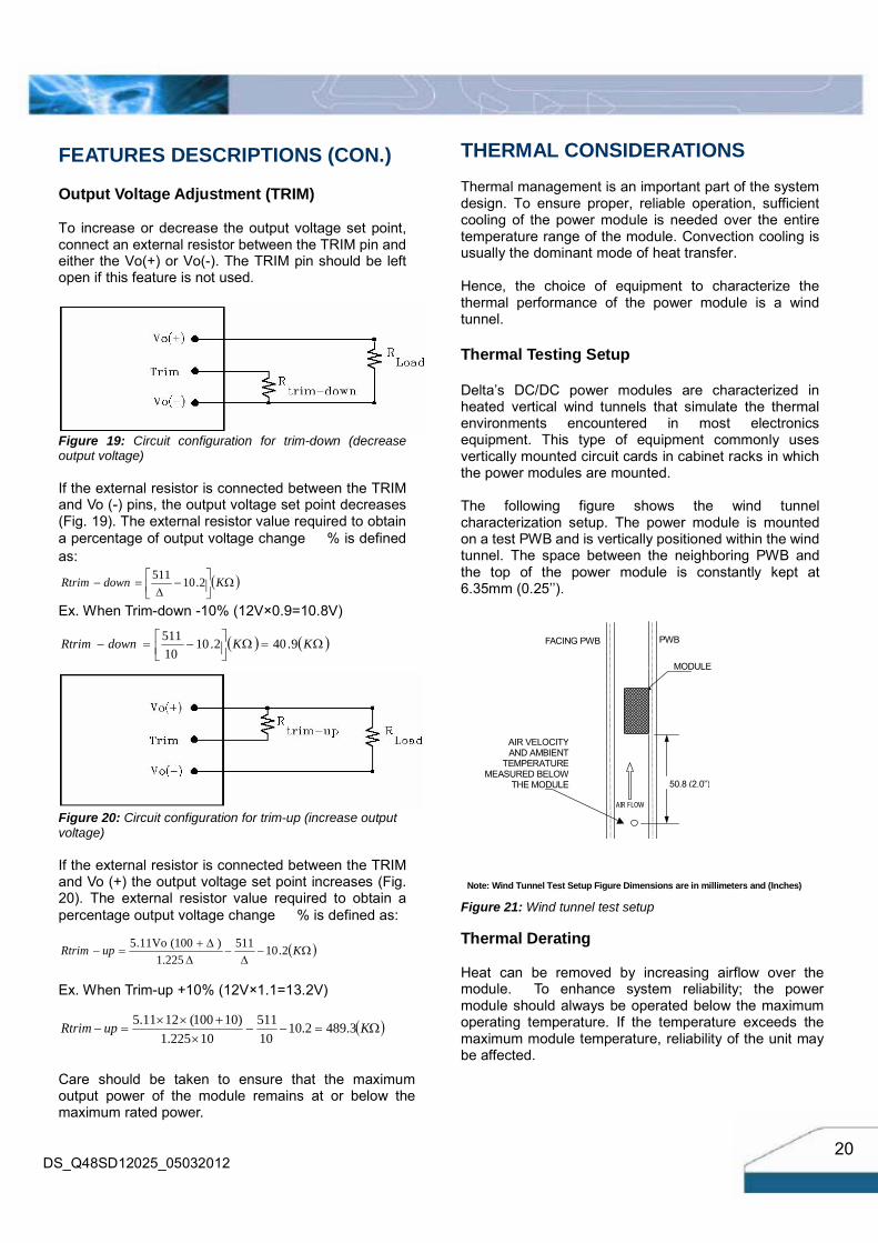
THERMAL CONSIDERATIONS Thermal management is an important part of the system design. To ensure proper, reliable operation, sufficient cooling of the power module is needed over the entire temperature range of the module. Convection cooling is usually the dominant mode of heat transfer. Hence, the choice of equipment to characterize the thermal performance of the power module is a wind tunnel. Thermal Testing Setup Delta’s DC/DC power modules are characterized in heated vertical wind tunnels that simulate the thermal environments encountered in most electronics equipment. This type of equipment commonly uses vertically mounted circuit cards in cabinet racks in which the power modules are mounted. The following figure shows the wind tunnel characterization setup. The power module is mounted on a test PWB and is vertically positioned within the wind tunnel. The space between the neighboring PWB and the top of the power module is constantly kept at 6.35mm (0.25’’).
Note: Wind Tunnel Test Setup Figure Dimensions are in millimeters and (Inches)
12.7 (0.5”)
MODULE
AIR FLOW
50.8 (2.0”)
FACING PWB PWB
AIR VELOCITYAND AMBIENT
TEMPERATURE MEASURED BELOW
THE MODULE
Figure 21: Wind tunnel test setup Thermal Derating Heat can be removed by increasing airflow over the module. To enhance system reliability; the power module should always be operated below the maximum operating temperature. If the temperature exceeds the maximum module temperature, reliability of the unit may be affected.

DS_Q48SD12025_05032012
21
THERMAL CURVES (WITHOUT HEAT SPREADER)
NTC RESI STOR
AIRFLOW
HOT SPOT 1
Figure 22: * Hot spot 1& NTC resistor temperature measured points
0
5
10
15
20
25
25 30 35 40 45 50 55 60 65 70 75 80 85
Output Current(A)
Ambient Temperature ()
Q48SD12025(Standard) Output Current vs. Ambient Temperature and Air Velocity@Vin = 48V (Transverse Orientation)
NaturalConvection
100LFM
200LFM
300LFM
400LFM
500LFM
600LFM
Figure 23: Output current vs. ambient temperature and air velocity @Vin=48V(Transverse Orientation, airflow from Vin+ to Vin-, without heat spreader)
THERMAL CURVES (WITH HEAT SPREADER)
AIRFLOW
HOT SPOT 2
Figure 24: * Hot spot 2 temperature measured point
0
5
10
15
20
25
25 30 35 40 45 50 55 60 65 70 75 80 85
Output Current(A)
Ambient Temperature ()
Q48SD12025(Standard) Output Current vs. Ambient Temperature and Air Velocity@Vin = 48V (Transverse Orientation,With Heat Spreader)
NaturalConvection
100LFM
200LFM
300LFM
400LFM
500LFM
Figure 25: Output current vs. ambient temperature and air velocity @Vin=48V(Transverse Orientation, airflow from Vin+ to Vin-,with heat spreader)

DS_Q48SD12025_05032012
22
MECHANICAL DRAWING (WITH HEAT SPREADER) *For modules with through-hole pins and the optional heat spreader, they are intended for wave soldering assembly
onto system boards, please do not subject such modules through reflow temperature profile.

DS_Q48SD12025_05032012
23
MECHANICAL DRAWING (WITHOUT HEAT SPREADER)
Pin Specification: Pins 1-3&5 1.00mm (0.040”) diameter (All pins are copper with matte Tin plating over Nickel under plating) Pins 4 &6 1.50mm (0.060”) diameter (All pins are copper with matte Tin plating over Nickel under plating) Pins 7-13 SQ 0.50mm(0.020’’) ( All pins are copper with gold flash plating)

DS_Q48SD12025_05032012
24
PART NUMBERING SYSTEM Q 48 S D 120 25 N R F A
Type of Product
Input Voltage
Number of Outputs
Product Series
Output Voltage
Output Current
ON/OFFLogic
Pin Length/Type Option Code
Current sharing
pin Trim pin PMBus
pin Heat
spreader
A Y N Y N B N Y N N C N Y N Y H Y N Y Y
Q- Quarter
Brick
48- 36~75V
S- Single D – Full digital control
120 - 12V 25- 25AN -
Negative
K – 0.110’’N - 0.145”R - 0.170”C - 0.181”S - 0.189”T - 0.220”L - 0.248”
F- RoHS 6/6(Lead Free)
G N Y Y Y
MODEL LIST MODEL NAME INPUT OUTPUT EFF @ 100% LOAD Q48SD12025NRFA 36V~75V 9A 12V 25A 95.7%
Default remote on/off logic is negative and pin length is 0.170” For different remote on/off logic and pin length, please refer to part numbering system above or contact your local sales office.
CONTACT: www.delta.com.tw/dcdc USA: Telephone: East Coast: 978-656-3993 West Coast: 510-668-5100 Fax: (978) 656 3964 Email: [email protected]
Europe: Telephone: +41 31 998 53 11 Fax: +41 31 998 53 53 Email: [email protected]
Asia & the rest of world: Telephone: +886 3 4526107 x 6220~6224Fax: +886 3 4513485 Email: [email protected]
WARRANTY Delta offers a two (2) year limited warranty. Complete warranty information is listed on our web site or is available upon request from Delta. Information furnished by Delta is believed to be accurate and reliable. However, no responsibility is assumed by Delta for its use, nor for any infringements of patents or other rights of third parties, which may result from its use. No license is granted by implication or otherwise under any patent or patent rights of Delta. Delta reserves the right to revise these specifications at any time, without notice.