Embed Size (px)
Citation preview
Digital Electronics Lab (15ECL38) 2017-18
Dept. of ECE, CIT, Gubbi Page 1
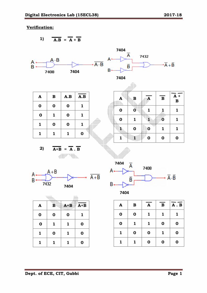
Verification:
1)
2)
A B A.B A.B
0 0 0 1
0 1 0 1
1 0 0 1
1 1 1 0
A B A B A + B
0 0 1 1 1
0 1 1 0 1
1 0 0 1 1
1 1 0 0 0
A B A+B A+B
0 0 0 1
0 1 1 0
1 0 1 0
1 1 1 0
A B A B A . B
0 0 1 1 1
0 1 1 0 0
1 0 0 1 0
1 1 0 0 0
A+B = A . B
A.B = A + B
7404
7404
7404
7404
7404
7404
Digital Electronics Lab (15ECL38) 2017-18
Dept. of ECE, CIT, Gubbi Page 2
Experiment No: 1(A) Date:
Demorgan’s Theorem for 2 variables
Aim: To verify Demorgan’s theorem for 2 variables
Components required: IC 7404, 7432, 7408, Digital IC Trainer Kit, Patch
cards
Theory:-
Theorem 1: The compliment of the product of two variables is equal to the
sum of the compliment of each variable. Thus according to De-Morgan’s
laws or De-Morgan's theorem if A and B are the two variables or Boolean
numbers. Then accordingly,
Theorem 2:-
The compliment of the sum of two variables is equal to the product of the
compliment of each variable. Thus according to De Morgan’s theorem if A
and B are the two variables then,
De-Morgan's laws can also be implemented in Boolean algebra in the
following steps:-
1. While doing Boolean algebra at first replace the given operator.
That is (+) is replaced with (.) and (.) is replaced with (+).
2. Compliment of each of the term is to be found.
Procedure:
1. Realize the Demorgans theorem using logic gates.
2. Connect VCC and ground as shown in the pin diagram.
3. Make connections as per the logic gate diagram.
4. Apply the different combinations of input according to the truth tables.
Verify that the results are correct.
A.B = A + B
A+B = A . B
Digital Electronics Lab (15ECL38) 2017-18
Dept. of ECE, CIT, Gubbi Page 3
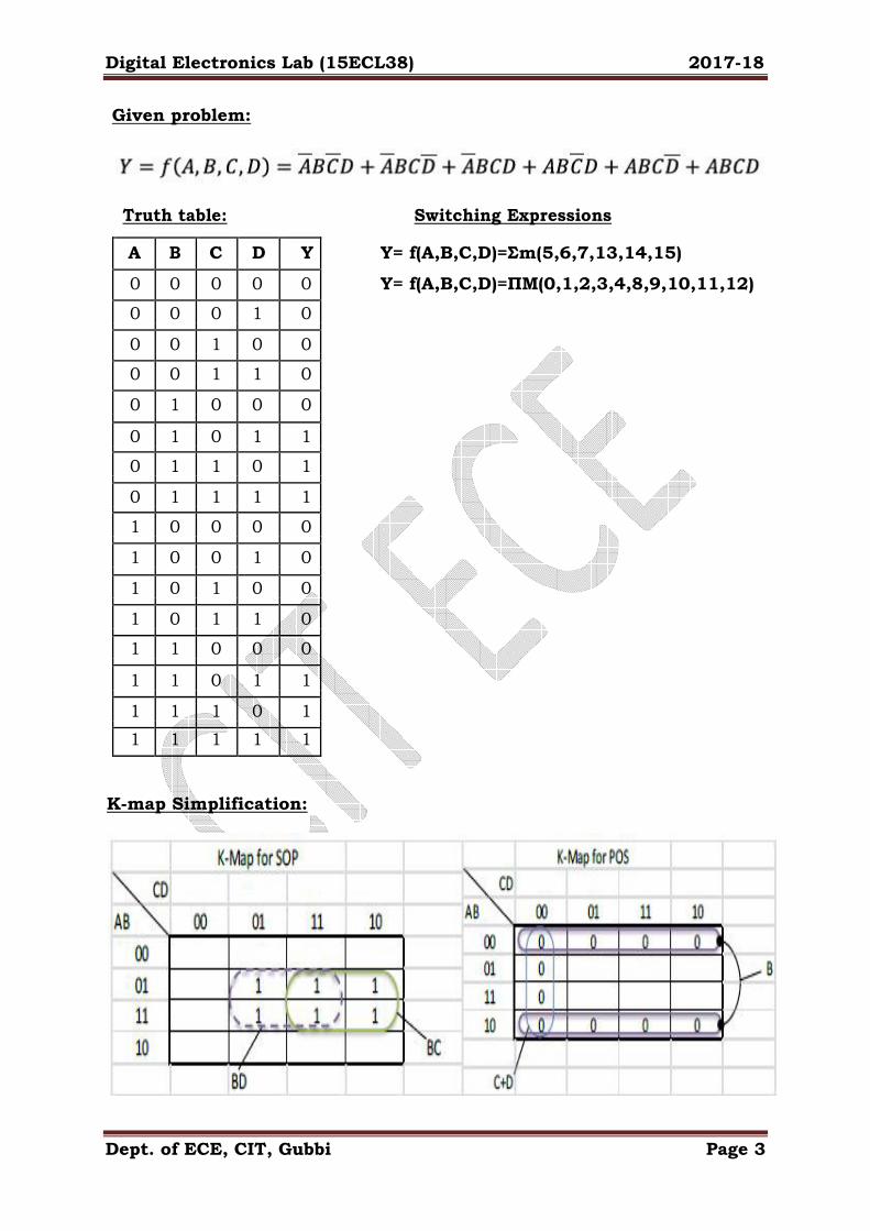
Given problem:
Truth table: Switching Expressions
A B C D Y Y= f(A,B,C,D)=Σm(5,6,7,13,14,15)
0 0 0 0 0 Y= f(A,B,C,D)=ΠM(0,1,2,3,4,8,9,10,11,12)
0 0 0 1 0
0 0 1 0 0
0 0 1 1 0
0 1 0 0 0
0 1 0 1 1
0 1 1 0 1
0 1 1 1 1
1 0 0 0 0
1 0 0 1 0
1 0 1 0 0
1 0 1 1 0
1 1 0 0 0
1 1 0 1 1
1 1 1 0 1
1 1 1 1 1
K-map Simplification:
Digital Electronics Lab (15ECL38) 2017-18
Dept. of ECE, CIT, Gubbi Page 4
Experiment No: 1(B) Date:
Sum of Product and Product of Sum
Aim: To design sum-of product and product-of-sum expressions using Basic
gates and Universal gates.
Components Required: IC 7408 (AND), IC 7404 (NOT), IC 7432 (OR), IC
7400 (NAND), IC 7402 (NOR), IC 7486 (EX-OR), IC Trainer Kit, Patch cards
Theory:
Canonical Forms (Normal Forms): Any Boolean function can be
written in disjunctive normal form (sum of min-terms) or conjunctive
normal form (product of max-terms). A Boolean function can be
represented by a Karnaugh map in which each cell corresponds to two
minterm. Sum of minterms : Sum Of Product (SOP) Product of maxterms : Product Of Sum (POS) Procedure: 1. Verify that the gates are working.
2. Construct a truth table for the given problem.
3. Draw a Karnaugh Map corresponding to the given truth table.
4. Simplify the given Boolean expression manually using the Karnaugh Map.
A. Implementation Using Logic Gates: 5. Realize the simplified expression using logic gates.
6. Connect VCC and ground as shown in the pin diagram.
7. Make connections as per the logic gate diagram.
8. Apply the different combinations of input according to the truth tables.
Verify that the results are correct.
B. Implementation Using Universal Gates:
1. Convert the AND-OR logic into NAND-NAND and NOR-NOR logic.
2. Realize the simplified Boolean expressions using only NAND gates, and
then using only NOR gates.
3. Connect the circuits according to the circuit diagrams, apply inputs
according to the truth table and verify the results.
Digital Electronics Lab (15ECL38) 2017-18
Dept. of ECE, CIT, Gubbi Page 5
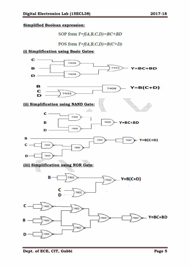
Simplified Boolean expression:
(i) Simplification using Basic Gates:
(ii) Simplification using NAND Gate:
(iii) Simplification using NOR Gate:
Digital Electronics Lab (15ECL38) 2017-18
Dept. of ECE, CIT, Gubbi Page 6
Result: Exercise:
An automobile alarm circuit is used to detect certain undesirable
conditions. Three switches are used to indicate the status of the door by the
driver’s seat, the ignition, and the headlights respectively. Design the logic
circuit with these three switches as inputs so that the alarm will be
activated whenever either of the following conditions exists:
• The headlights are on while the ignition is off
• The door is open while ignition is on.
Digital Electronics Lab (15ECL38)
Dept. of ECE, CIT, Gubbi
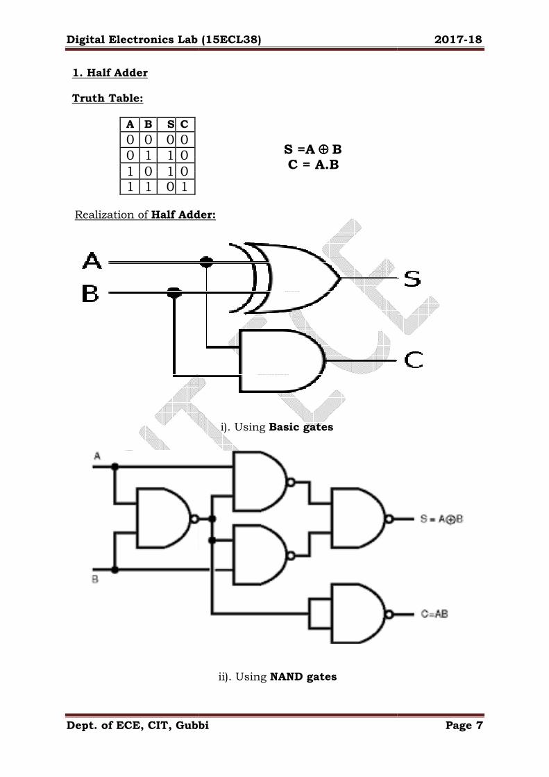
1. Half Adder
Truth Table:
A B S C
0 0 0 0
0 1 1 0
1 0 1 0
1 1 0 1
Realization of Half Adder:
Digital Electronics Lab (15ECL38)
Dept. of ECE, CIT, Gubbi
S =A ⊕ ⊕ ⊕ ⊕ B
C = A.B
Half Adder:
i). Using Basic gates
ii). Using NAND gates
2017-18
Page 7
Digital Electronics Lab (15ECL38) 2017-18
Dept. of ECE, CIT, Gubbi Page 8
Experiment No: 2 Date:
ADDERS AND SUBTRACTORS
Aim: (i) To realize half/full adder using Logic gates & NAND gates
(ii) To realize half/full Subtractor using Logic gates & NAND gates
Components Required: IC 7408, IC 7432, IC 7486, IC 7404, IC 7400, Patch chords
Theory:
Half-Adder: A combinational logic circuit that performs the addition of two
data bits, A and B, is called a half-adder. Addition will result in two output
bits; one of which is the sum bit S, and the other is the carry bit, C. The
Boolean functions describing the half-adder are: S =A ⊕ B
C = A.B
Full-Adder: The half-adder does not take the carry bit from its previous
stage into account. This carry bit from its previous stage is called carry-in
bit. A combinational logic circuit that adds two data bits, A and B, and a
carry-in bit, Cin , is called a full-adder. The Boolean functions describing
the full-adder are:
S = A ⊕ B ⊕ Cin
C = A.B+ Cin (A ⊕ B)
Half Subtractor: Subtracting a single-bit binary value B from another A
(i.e. A -B) produces a difference bit D and a borrow out bit Br. This
operation is called half subtraction and the circuit to realize it is called a
half subtractor. The
Boolean functions describing the half-Subtractor are:
D =A ⊕ B
Br= A’.B
Full Subtractor: Subtracting two single-bit binary values, B, Cin from a
single-bit value A produces a difference bit D and a borrow out Br bit. This
is called full subtraction. The Boolean functions describing the full-
subtractor
are:
D = A ⊕ B ⊕ Cin
Br= A’.B + A’.Cin + B.Cin
Digital Electronics Lab (15ECL38)
Dept. of ECE, CIT, Gubbi
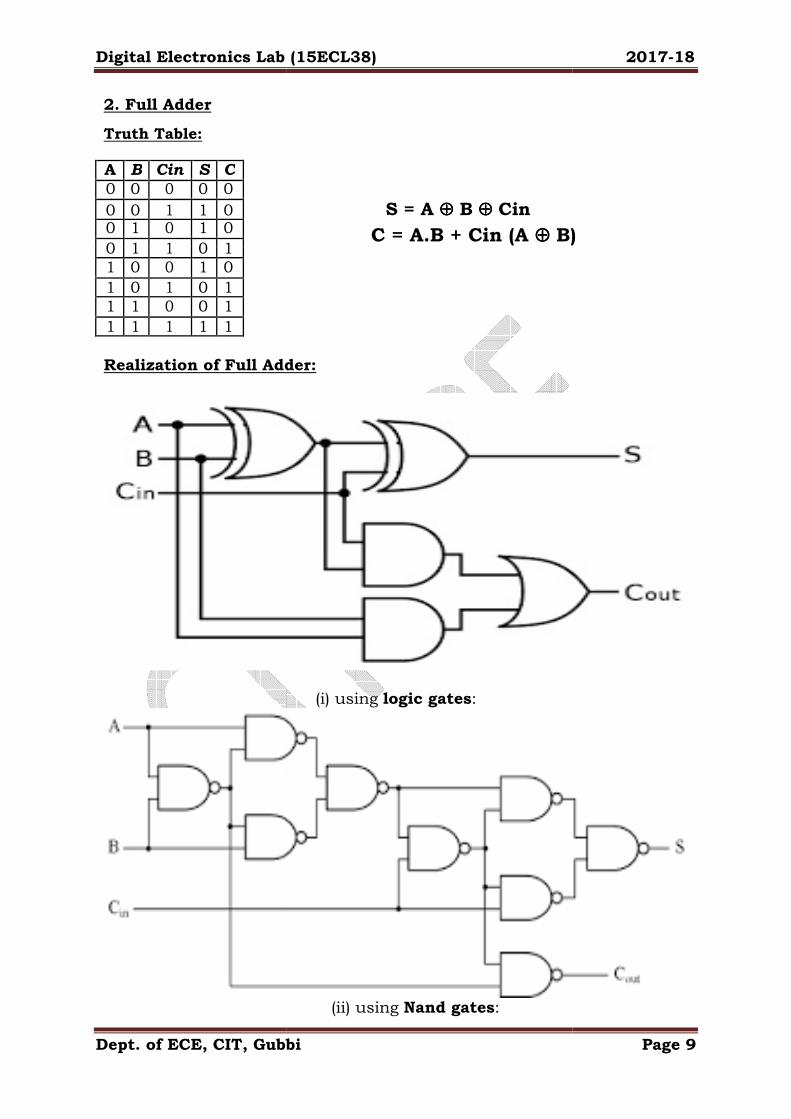
2. Full Adder
Truth Table:
A B Cin S C
0 0 0 0 0
0 0 1 1 0
0 1 0 1 0
0 1 1 0 1
1 0 0 1 0
1 0 1 0 1
1 1 0 0 1
1 1 1 1 1
Realization of Full Adder
Digital Electronics Lab (15ECL38)
Dept. of ECE, CIT, Gubbi
S = A ⊕⊕⊕⊕ B ⊕⊕⊕⊕ Cin
C = A.B + Cin (A ⊕⊕⊕⊕ B)
Full Adder:
(i) using logic gates:
(ii) using Nand gates:
2017-18
Page 9
B)
Digital Electronics Lab (15ECL38) 2017-18
Dept. of ECE, CIT, Gubbi Page 10
Procedure:
1. Verify that the gates are working.
2. Make the connections as per the circuit diagram for the half adder circuit, on the trainer kit.
3. Switch on the VCC power supply and apply the various combinations
of the inputs according to the respective truth tables.
4. Verify that the outputs are according to the expected results.
5. Repeat the procedure for the full adder circuit, the half subtractor
and full subtractor circuits.
6. Verify that the sum/difference and carry/borrow bits are according to
the expected values.
Digital Electronics Lab (15ECL38) 2017-18
Dept. of ECE, CIT, Gubbi Page 11
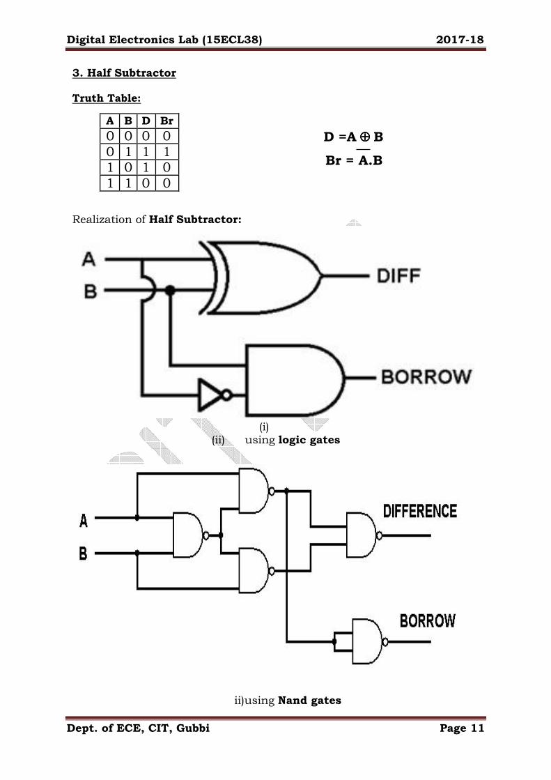
3. Half Subtractor
Truth Table:
Realization of Half Subtractor:
(i)
(ii) using logic gates
ii)using Nand gates
A B D Br
0 0 0 0
0 1 1 1
1 0 1 0
1 1 0 0
D =A ⊕ ⊕ ⊕ ⊕ B
Br = A.B
Digital Electronics Lab (15ECL38) 2017-18
Dept. of ECE, CIT, Gubbi Page 12
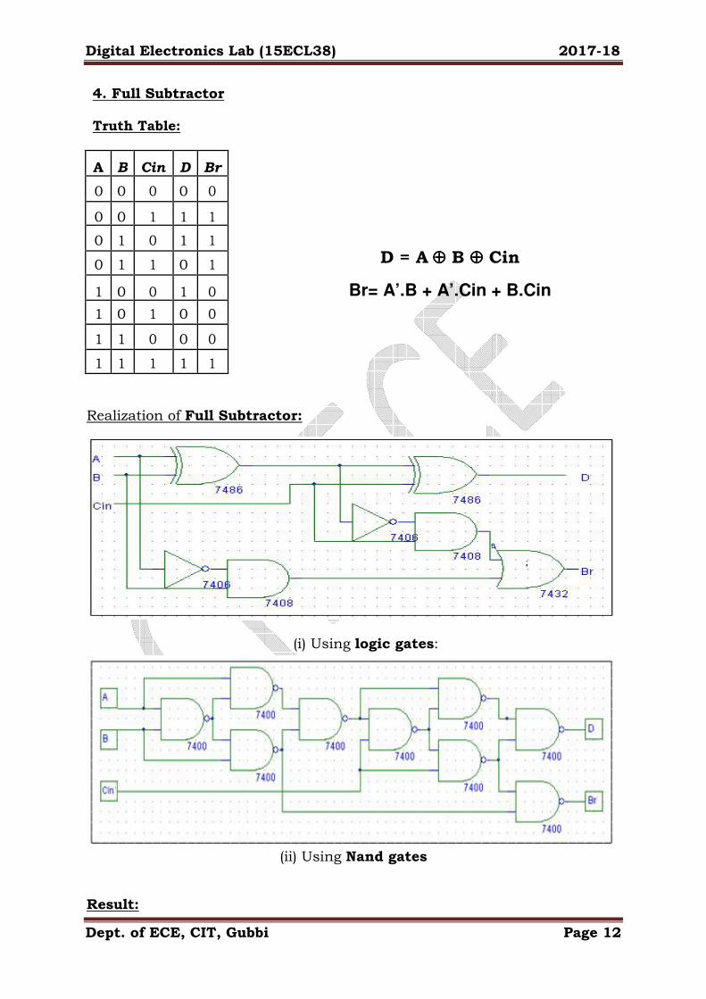
4. Full Subtractor
Truth Table:
A B Cin D Br
0 0 0 0 0
0 0 1 1 1
0 1 0 1 1
D = A ⊕ ⊕ ⊕ ⊕ B ⊕⊕⊕⊕ Cin
0 1 1 0 1
Br= A’.B + A’.Cin + B.Cin
1 0 0 1 0
1 0 1 0 0
1 1 0 0 0
1 1 1 1 1
Realization of Full Subtractor:
(i) Using logic gates:
(ii) Using Nand gates
Result:
Digital Electronics Lab (15ECL38)
Dept. of ECE, CIT, Gubbi
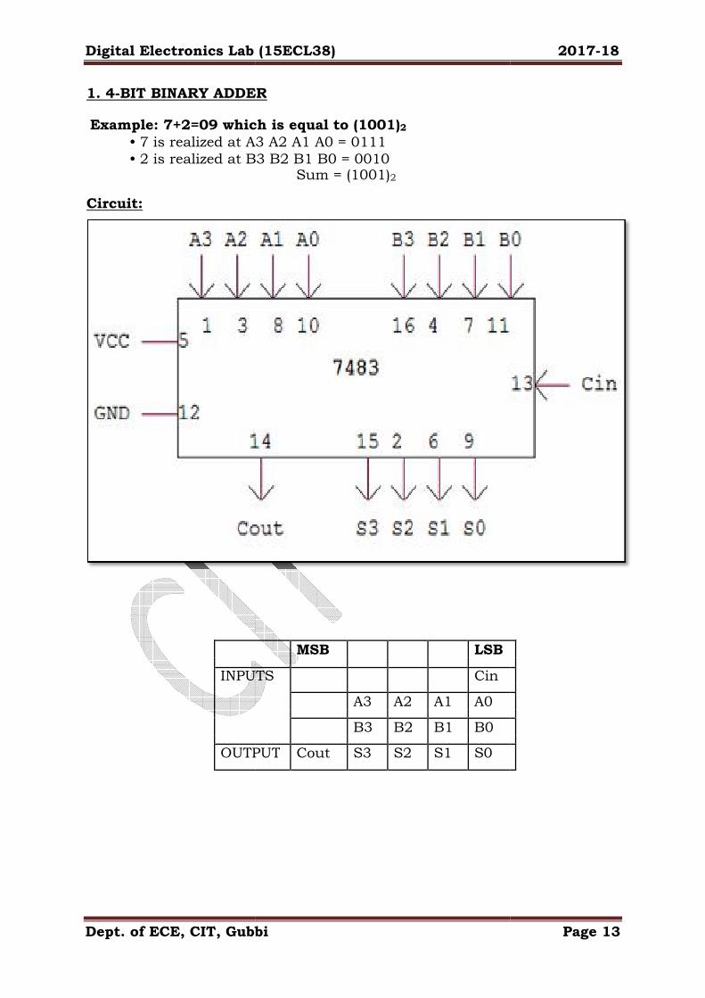
1. 4-BIT BINARY ADDER
Example: 7+2=09 which is equal to (1001)
• 7 is realized at A3 A2 A1 A0 = 0111 • 2 is realized at B3 B2 B1 B0 = 0010
Circuit:
INPUTS
OUTPUT
Digital Electronics Lab (15ECL38)
Dept. of ECE, CIT, Gubbi
BIT BINARY ADDER
Example: 7+2=09 which is equal to (1001)2
7 is realized at A3 A2 A1 A0 = 0111
2 is realized at B3 B2 B1 B0 = 0010 Sum = (1001)2
MSB LSB
INPUTS Cin
A3 A2 A1 A0
B3 B2 B1 B0
OUTPUT Cout S3 S2 S1 S0
2017-18
Page 13
Digital Electronics Lab (15ECL38)
Dept. of ECE, CIT, Gubbi
Experiment No: 3 Date:
PARALLEL ADDER AND SUBTRACTOR USING 7483
Aim: To design and set up the following
i) A 4-bit binary parallel adder.
ii) A 4-bit binary parallel subtractor.
Components Required:
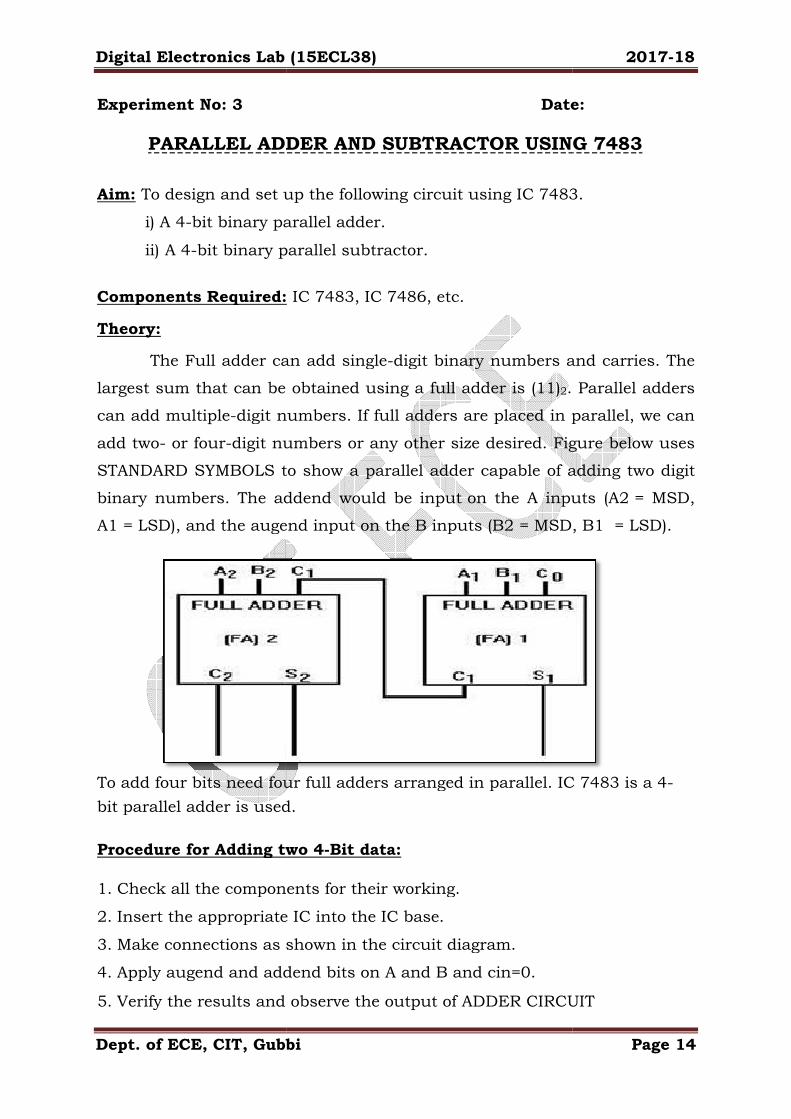
Theory:
The Full adder can add single
largest sum that can be obtained
can add multiple-digit numbers. If full adders are placed in parallel, we can
add two- or four-digit numbers or any other size desired. Figure below uses
STANDARD SYMBOLS to show a parallel adder capable of addi
binary numbers. The addend would be input
A1 = LSD), and the augend input on the B inputs (B2
To add four bits need four full adders arranged in parallel. IC 7483 is a 4
bit parallel adder is used.
Procedure for Adding two 4
1. Check all the components for their working. 2. Insert the appropriate IC into the IC base. 3. Make connections as shown in the circuit diagram. 4. Apply augend and addend bits on A and B and cin=0 5. Verify the results and observe the output of ADDER CIRCUIT
Digital Electronics Lab (15ECL38)
Dept. of ECE, CIT, Gubbi
3 Date:
PARALLEL ADDER AND SUBTRACTOR USING 7483
To design and set up the following circuit using IC 7483.
bit binary parallel adder.
bit binary parallel subtractor.
Components Required: IC 7483, IC 7486, etc.
The Full adder can add single-digit binary numbers and carries. The
largest sum that can be obtained using a full adder is (11)2. Parallel adders
digit numbers. If full adders are placed in parallel, we can
digit numbers or any other size desired. Figure below uses
STANDARD SYMBOLS to show a parallel adder capable of addi
The addend would be input on the A inputs (A2
= LSD), and the augend input on the B inputs (B2 = MSD, B1
To add four bits need four full adders arranged in parallel. IC 7483 is a 4
parallel adder is used.
Procedure for Adding two 4-Bit data:
Check all the components for their working.
Insert the appropriate IC into the IC base.
Make connections as shown in the circuit diagram.
Apply augend and addend bits on A and B and cin=0.
Verify the results and observe the output of ADDER CIRCUIT
2017-18
Page 14
3 Date:
PARALLEL ADDER AND SUBTRACTOR USING 7483
circuit using IC 7483.
digit binary numbers and carries. The
. Parallel adders
digit numbers. If full adders are placed in parallel, we can
digit numbers or any other size desired. Figure below uses
STANDARD SYMBOLS to show a parallel adder capable of adding two digit
inputs (A2 = MSD,
= MSD, B1 = LSD).
To add four bits need four full adders arranged in parallel. IC 7483 is a 4-
Verify the results and observe the output of ADDER CIRCUIT
Digital Electronics Lab (15ECL38)
Dept. of ECE, CIT, Gubbi
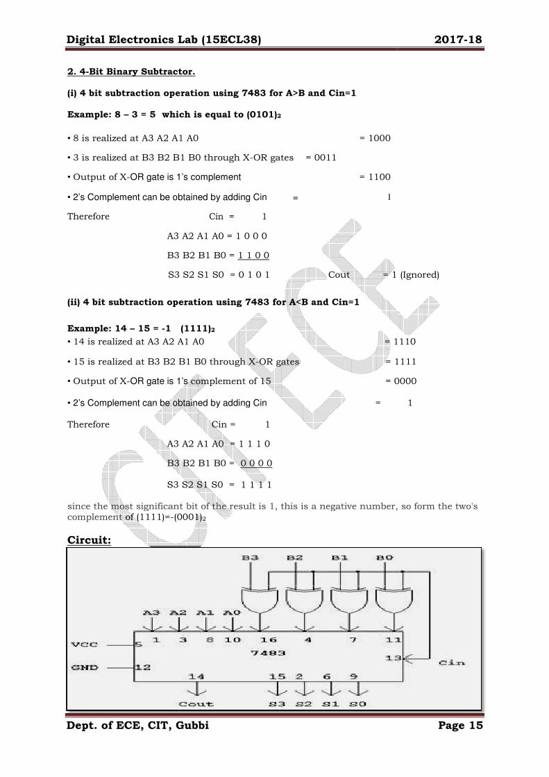
2. 4-Bit Binary Subtractor.
(i) 4 bit subtraction operation using 7483 for A>B and Cin=1
Example: 8 – 3 = 5 which is equal to (0101)
• 8 is realized at A3 A2 A1 A0
• 3 is realized at B3 B2 B1 B0 through X
• Output of X-OR gate is 1’s complement
• 2’s Complement can be obtained by adding Cin =
Therefore
A3 A2 A1 A0 = 1 0 0 0
B3 B2 B1 B0 =
S3 S2 S1 S0 = 0 1 0 1
(ii) 4 bit subtraction operation using 7483 for A<B and Cin=1
Example: 14 – 15 = -1 (1111)
• 14 is realized at A3 A2 A1 A0
• 15 is realized at B3 B2 B1 B0 through
• Output of X-OR gate is 1’s complement of 15
• 2’s Complement can be obtained by adding Cin
Therefore
A3 A2 A1 A0
B3 B2 B1 B0 =
S3 S2 S1 S0 = 1 1 1 1
since the most significant bit of the result is 1, this is a negative number, so form the two's complement of (1111)=-(0001)
Circuit:
Digital Electronics Lab (15ECL38)
Dept. of ECE, CIT, Gubbi
(i) 4 bit subtraction operation using 7483 for A>B and Cin=1
3 = 5 which is equal to (0101)2
8 is realized at A3 A2 A1 A0 = 1000
is realized at B3 B2 B1 B0 through X-OR gates = 0011
OR gate is 1’s complement = 1100
• 2’s Complement can be obtained by adding Cin = 1
Cin = 1
A3 A2 A1 A0 = 1 0 0 0
B3 B2 B1 B0 = 1 1 0 0
S3 S2 S1 S0 = 0 1 0 1 Cout = 1 (Ignored)
(ii) 4 bit subtraction operation using 7483 for A<B and Cin=1
1 (1111)2
14 is realized at A3 A2 A1 A0 = 1110
15 is realized at B3 B2 B1 B0 through X-OR gates = 1111
complement of 15 = 0000
• 2’s Complement can be obtained by adding Cin
=
Cin =
1
A3 A2 A1 A0 = 1 1 1 0
B3 B2 B1 B0 = 0 0 0 0
S3 S2 S1 S0 = 1 1 1 1
since the most significant bit of the result is 1, this is a negative number, so form the two's (0001)2
2017-18
Page 15
= 1 (Ignored)
= 1110
= 1111
= 0000
1
since the most significant bit of the result is 1, this is a negative number, so form the two's
Digital Electronics Lab (15ECL38) 2017-18
Dept. of ECE, CIT, Gubbi Page 16
Procedure for subtracting two 4-Bit data:
1. Check all the components for their working. 2. Insert the appropriate IC into the IC base. 3. Make connections as shown in the circuit diagram. 4. Apply Minuend and subtrahend bits on A and B and cin=1. 5. Verify the results and observe the outputs.
Result:
Digital Electronics Lab (15ECL38)
Dept. of ECE, CIT, Gubbi
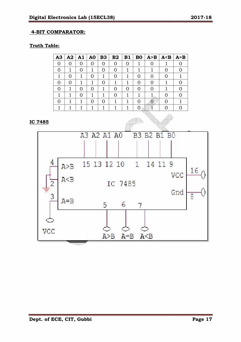
4-BIT COMPARATOR:
Truth Table:
A3 A2 A1
0 0 0
0 1 0
1 0 1
0 0 1
0 1 0
1 1 0
0 1 1
1 1 1 IC 7485
Digital Electronics Lab (15ECL38)
Dept. of ECE, CIT, Gubbi
A0 B3 B2 B1 B0 A>B A<B
0 0 0 0 1 0 1
1 0 0 1 1 1 0
0 1 0 1 0 0 0
1 0 1 1 0 0 1
0 1 0 0 0 0 1
1 1 0 1 1 1 0
0 0 1 1 0 0 0
1 1 1 1 0 1 0
2017-18
Page 17
A=B
0
0
1
0
0
0
1
0
Digital Electronics Lab (15ECL38) 2017-18
Dept. of ECE, CIT, Gubbi Page 18
Experiment No: 4 Date:
COMPARATORS Aim: To realize One & Two Bit Comparator and study of 7485 magnitude
comparator.
Components required: IC 7485, Patch Cards & IC Trainer Kit. Theory:
Magnitude Comparator is a logical circuit, which compares two
signals A and B and generates three logical outputs, whether A > B, A = B,
or A < B. IC 7485 is a high speed 4-bit Magnitude comparator, which
compares two 4-bit words. The A = B Input must be held high for proper
compare operation.
Result: Exercise A simple security system for two doors consists of a card reader and a
keypad. A person may open a particular door if he or she has a card
containing the corresponding code and enters an authorized code for that
card. The output from the card reader are as follows.
To unlock a door, a person must hold down the proper keys on the keypad
and then insert the card in the reader. The authorized keypad codes for door
1 are 101 and 110, and the authorized keypad codes for door 2 are 101 and
011. If the card has an invalid code or if the wrong keypad code is entered,
the alarm will ring when card is inserted. If the correct keypad code is
entered, the corresponding door will be unlocked when the card is inserted.
Action A B
No card inserted 0 0
Valid Code for Door 1 0 1
Valid Code for Door2 1 1
Invalid card code 1 0
Digital Electronics Lab (15ECL38)
Dept. of ECE, CIT, Gubbi
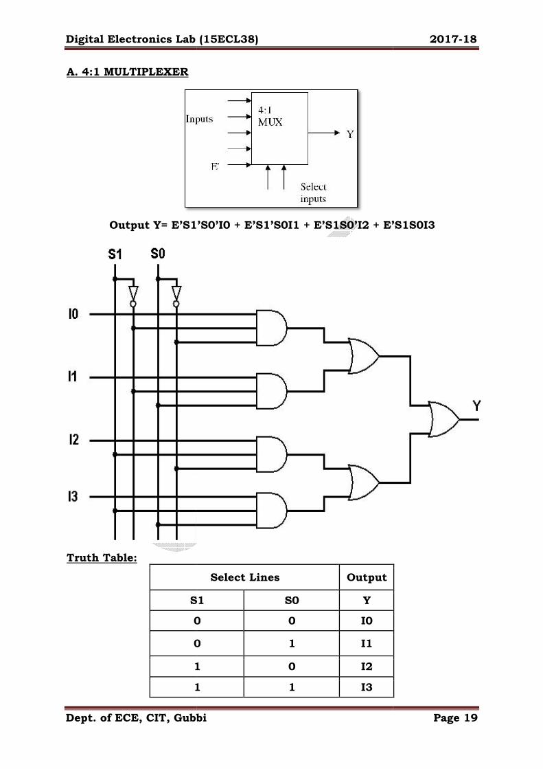
A. 4:1 MULTIPLEXER
Output Y= E’S1
Truth Table:
S1
0
0
1
1
Digital Electronics Lab (15ECL38)
Dept. of ECE, CIT, Gubbi
S1’S0’I0 + E’S1’S0I1 + E’S1S0’I2 + E’
Select Lines Output
S1 S0 Y
0 0 I0
0 1 I1
1 0 I2
1 1 I3
2017-18
Page 19
’S1S0I3
Digital Electronics Lab (15ECL38) 2017-18
Dept. of ECE, CIT, Gubbi Page 20
Experiment No: 5(a) Date:
4:1 MULTIPLEXER USING GATES
Aim: To design and set up a 4:1 Multiplexer (MUX) using gates. Components Required: IC 74153, IC 7404, 7432, 7411 and Patch Cords &
IC Trainer Kit.
Theory:
Multiplexers are very useful components in digital systems. They
transfer a large number of information units over a smaller number of
channels, (usually one channel) under the control of selection signals. Multiplexer means many to one. A multiplexer is a circuit with many inputs
but only one output. By using control signals (select lines) we can select any
input to the output. Multiplexer is also called as data selector because the
output bit depends on the input data bit that is selected. The general
multiplexer circuit has 2n input signals, n control/select signals and 1
output signal. Procedure: 1. The connection is made as shown in the diagram.
2. Here, S1 and S0 are the channel selection lines, I0, I1, I2, I3 are the
respective data lines of the channels and Y is the output.
3. Based on the selection lines one of the inputs will be selected at the output,
and thus the truth table is verified.

Digital Electronics Lab (15ECL38)
Dept. of ECE, CIT, Gubbi
B. 3 Variable function using IC 74151
Truth table:
C
0
0
0
0
1
1
1
1
Digital Electronics Lab (15ECL38)
Dept. of ECE, CIT, Gubbi
B. 3 Variable function using IC 74151
Select Lines Output
B A Y
0 0 0
0 1 1
1 0 1
1 1 0
0 0 0
0 1 0
1 0 0
1 1 1
2017-18
Page 21
Output
Y
0
1
1
0
0
0
0
1
Digital Electronics Lab (15ECL38) 2017-18
Dept. of ECE, CIT, Gubbi Page 22
Experiment No: 5(b) Date:
8:1 MULTIPLEXER USING 74151
Aim: To design and set up the following circuit
3 variable function using IC 74151 (8:1 MUX)
Components Required: IC 74151, Patch Cords & IC Trainer Kit.
Procedure: 1. For the given expression, a truth table is to be written.
2. An expression in SOP format is to be written.
3. The connection is made according to the obtained expression.
4. The truth table is verified for that particular expression.
Result:
Digital Electronics Lab (15ECL38)
Dept. of ECE, CIT, Gubbi
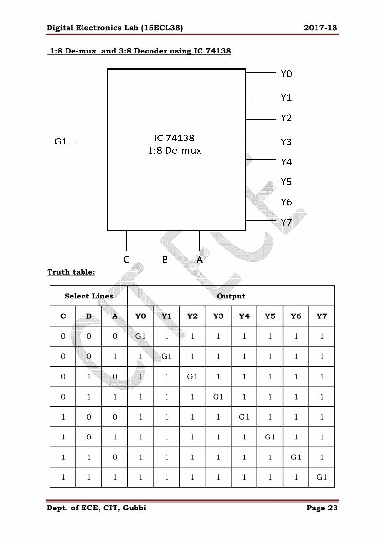
1:8 De-mux and 3:8 Decoder
Truth table:
Select Lines
C B A Y0
0 0 0 G1
0 0 1 1
0 1 0 1
0 1 1 1
1 0 0 1
1 0 1 1
1 1 0 1
1 1 1 1
Digital Electronics Lab (15ECL38)
Dept. of ECE, CIT, Gubbi
and 3:8 Decoder using IC 74138
Output
Y0 Y1 Y2 Y3 Y4 Y5
G1 1 1 1 1 1
1 G1 1 1 1 1
1 1 G1 1 1 1
1 1 1 G1 1 1
1 1 1 1 G1 1
1 1 1 1 1 G1
1 1 1 1 1 1
1 1 1 1 1 1
2017-18
Page 23
Y6 Y7
1 1
1 1
1 1
1 1
1 1
1 1
G1 1
1 G1
Digital Electronics Lab (15ECL38) 2017-18
Dept. of ECE, CIT, Gubbi Page 24
Experiment No: 6 Date:
1:8 DEMUX AND 3:8 DECODER USING IC 74138
Aim: To design 1:8 Demux and 3:8 Decoder using IC 74138
Components Required: IC 74138, Patch Cords & IC Trainer Kit.
Theory:
A demultiplexer (or demux) is a device that takes a single input line and
routes it to one of several digital output lines. A demultiplexer of 2n outputs
has n select lines, which are used to select which output line to send the
input. A demultiplexer is also called a data distributor.
A decoder is a circuit which has n inputs and 2n outputs, and outputs 1 on
the wire corresponding to the binary number represented by the inputs. A
standard decoder typically has an additional input called Enable. Output is
only generated when the Enable input is activated.
Procedure (1:8 Demux): 1. The pins indicated as A, B and C are the selection lines, G1 acts as an
input line, Y0 to Y7 are the output channels.
2. A particular channel can be selected by choosing the proper bits for A, B
and C lines.
3. As IC 74138 is having active low outputs, initially all the outputs will be
high
4. Based on the bit given to G1 after selecting the channel, the same bit will
be reflected in that particular channel.
5. The truth table is verified for different combination of bits on both
selection lines and input G1.
NOTE: HERE PIN E1 = G1 AND PINS E2’ AND E3’ SHOULD BE
CONNECTED TO GROUND
Digital Electronics Lab (15ECL38)
Dept. of ECE, CIT, Gubbi
Truth table:
Enable Select Lines
E3 E2 E1 C B
1 X X X X
X 1 X X X
X X 0 X X
0 0 1 0 0
0 0 1 0 0
0 0 1 0 1
0 0 1 0 1
0 0 1 1 0
0 0 1 1 0
0 0 1 1 1
0 0 1 1 1
E1
E3
Digital Electronics Lab (15ECL38)
Dept. of ECE, CIT, Gubbi
Select Lines
Output
B A Y0 Y1 Y2 Y3 Y4
X X 1 1 1 1 1
X X 1 1 1 1 1
X X 1 1 1 1 1
0 0 0 1 1 1 1
0 1 1 0 1 1 1
1 0 1 1 0 1 1
1 1 1 1 1 0 1
0 0 1 1 1 1 0
0 1 1 1 1 1 1
1 0 1 1 1 1 1
1 1 1 1 1 1 1
2017-18
Page 25
Y5 Y6 Y7
1 1 1
1 1 1
1 1 1
1 1 1
1 1 1
1 1 1
1 1 1
1 1 1
0 1 1
1 0 1
1 1 0
Digital Electronics Lab (15ECL38) 2017-18
Dept. of ECE, CIT, Gubbi Page 26
Procedure (3:8 DECODER): 1. The connections are made as shown in the diagram
2. Enable pins are used to enable the IC
3. Using Select inputs, a particular output is selected.
4. Since IC 74138 is having an active low output, the particular line will
give a digital low.
Result:
Digital Electronics Lab (15ECL38)
Dept. of ECE, CIT, Gubbi
1. SR FLIPFLOP: Truth table:
Clk S
X 0
0
0
1
1
Digital Electronics Lab (15ECL38)
Dept. of ECE, CIT, Gubbi
R Q Q’
0 Q Q’
0 Q Q’
1 0 1
0 1 0
1 - -
2017-18
Page 27
States
No Change
No Change
Reset
Set
Invalid
Digital Electronics Lab (15ECL38) 2017-18
Dept. of ECE, CIT, Gubbi Page 28
Experiment No: 7 Date:
FLIP FLOPS Aim: To realize the following Flip-flops using NAND gates:
A. Clocked SR Flip-flop
B. JK Flip-flop Components required: IC 7410, IC7400 Theory:
A flip-flop is a circuit that has two stable states and can be used to
store state information. A flip-flop is a bistable multivibrator. The circuit
can be made to change state by signals applied to one or more control
inputs and will have one or two outputs. It is the basic storage element in
sequential logic. Flip-flops and latches are a fundamental building block of
digital electronics systems used in computers, communications, and many
other types of systems.
A flip–flop is a “bit bucket”; it holds a single binary bit .Flip flops are
actually an application of logic gates. With the help of Boolean logic we can
create memory with them. Flip flops can also be considered as the most
basic idea of a Random Access Memory [RAM].
The most commonly used application of flip flops is in the
implementation of a feedback circuit. As a memory relies on the feedback
concept, flip flops can be used to design it.
Procedure: 1. Make the connections as shown in the circuit diagrams. 2. Apply inputs as shown in the truth tables,
3. Check the outputs of the circuits; verify that they match wit5h the truth
tables.
Digital Electronics Lab (15ECL38) 2017-18
Dept. of ECE, CIT, Gubbi Page 29
2. JK FLIPFLOP:
Clk J K Q Q’ States
X 0 0 Q Q’ No Change
0 0 Q Q’ No Change
0 1 0 1 Reset
1 0 1 0 Set
1 1 Q’ Q Toggle
Digital Electronics Lab (15ECL38) 2017-18
Dept. of ECE, CIT, Gubbi Page 30
Result:
Digital Electronics Lab (15ECL38)
Dept. of ECE, CIT, Gubbi
1. SERIAL INPUT SERIAL OUTPUT (SISO):
Truth Table:
CLK
1
2
3
4
5
6
7
Digital Electronics Lab (15ECL38)
Dept. of ECE, CIT, Gubbi
1. SERIAL INPUT SERIAL OUTPUT (SISO):
CLK Serial I/P
Q3 Q2 Q1 Q0
D0=0 0 X X X
D1=1 1 0 X X
D2=1 1 1 0 X
D3=1 1 1 1 0=D0
X X 1 1 1=D1
X X X 1 1=D2
X X X X 1=D3
2017-18
Page 31
Digital Electronics Lab (15ECL38) 2017-18
Dept. of ECE, CIT, Gubbi Page 32
Experiment No: 8 Date:
SHIFT REGISTERS
Aim: To study IC 7474, and the realization of SIPO, SISO, PISO, PIPO
operations using the same.
Components required: IC 7474, patch cards etc. Theory:
• A shift register is a group of flip-flops (typically 4 or 8) that are
arranged so that the values stored in the flip-flops are shifted from
one flip-flop to the next for every clock.
• Shift registers are used extensively in logic circuits to control digital
displays.
• A classic example is numbers being typed into a calculator. As the
numbers are entered, the digits shift to the left one position. This
shifting is controlled by a shift register.
1. SERIAL INPUT SERIAL OUTPUT (SISO): Procedure:
1. Connections are made as shown in the SISO circuit diagram.
2. The shift register is loaded with 4 bits of data one by one serially.
3. At the end of the 4th clock pulse, the first data ‘d0’ appears at Q0.
4. Applying another clock pulse will push the second data bit, ‘d1’ to
Q0.
5. Applying yet another clock pulse gives the third data bit, ‘d2’ at Q0,
and so on.

Digital Electronics Lab (15ECL38) 2017-18
Dept. of ECE, CIT, Gubbi Page 33
2. SERIAL INPUT PARALLEL OUTPUT (SIPO): Truth Table:
CLK Serial I/P
Q3 Q2 Q1 Q0
1 1 1 X X X
2 0 0 1 X X
3 1 1 0 1 X
4 1 1 1 0 1
3. PARALLEL INPUT PARALLEL OUTPUT (PIPO): Truth Table:
Parallel I/P Parallel O/P
CLK D3 D2 D1 D0 Q3 Q2 Q1 Q0
1 1 0 1 1 1 0 1 1
Digital Electronics Lab (15ECL38) 2017-18
Dept. of ECE, CIT, Gubbi Page 34
2. SERIAL INPUT PARALLEL OUTPUT (SIPO): Procedure:
1. Connections are made as shown in the SIPO circuit diagram.
2. On applying the first bit of data and then a clock pulse, it can be
observed that this data appears at (Q3).
3. Now, applying the second bit of data and a clock pulse, the bit at Q3
shifts to Q2 and Q3 will be loaded with the new data.
4. This repeats until all 4 data bits are loaded.
5. At the end of the 4th clock pulse, all 4 bits are available at the parallel
output pins Q3 through Q0.
3. PARALLEL INPUT PARALLEL OUTPUT (PIPO):
Procedure:
1. Connections are made as shown in the PIPO mode circuit diagram.
2. Apply the 4 data bits as input to D3, D2, D1, D0.
3. Apply one clock pulse
4. Note that the 4 bit data at parallel inputs appears at the
parallel output pins Q3, Q2, Q1, Q0 respectively.
Digital Electronics Lab (15ECL38) 2017-18
Dept. of ECE, CIT, Gubbi Page 35
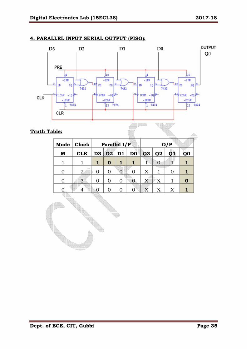
4. PARALLEL INPUT SERIAL OUTPUT (PISO): Truth Table:
Mode Clock Parallel I/P O/P
M CLK D3 D2 D1 D0 Q3 Q2 Q1 Q0
1 1 1 0 1 1 1 0 1 1
0 2 0 0 0 0 X 1 0 1
0 3 0 0 0 0 X X 1 0
0 4 0 0 0 0 X X X 1
D3 D2 D1 D0 Q0
Digital Electronics Lab (15ECL38) 2017-18
Dept. of ECE, CIT, Gubbi Page 36
4. PARALLEL INPUT SERIAL OUTPUT (PISO): Procedure: 1. Connections are made as shown in the PISO circuit diagram.
2. Apply the 4-bit data at the parallel I/P pins D3, D2, D1, D0 and apply single clock pulse to load the data to all 4 registers.
3. Now make all data bits as 0 and apply clock pulse one by one to get the data bit by bit at the output line.
4. The data applied at the parallel input pins will shift and comes out
serially at the output line Q0. NOTE: Here there is no Mode ‘M’ pin. It just indicates the status of loading
the data and shifting the data. M – 1 indicates data loading operation.
M -- 0 indicates shifting operation. Result: Exercise:
A shifter is a combinational network capable of shifting of 0’s and 1’s
to the left or right, leaving vacancies, by a fixed number of places as a result
of control signal. For example, assuming vacated positions are replaced by
0’s, the string 0011 when shifted right by 1 bit position becomes 0001 and
when shifted left by 1 bit position becomes 0110. A shifter to handle an n –
bit string can be readily designed with n multiplexers. Bits from the string
are applied to the data input lines. The control signals for the various
actions are applied to the select input lines. The shifted string appears on
the output lines. Design a shifter for handling a 4 bit string where table
indicates the control signals and desired actions. Vacated positions should
be filled with 0’s.
S1 S0 Action
0 0 No change
0 1 Shift right 1 bit position
1 0 Shift left 1 bit position
1 1 Clear data
Digital Electronics Lab (15ECL38) 2017-18
Dept. of ECE, CIT, Gubbi Page 37
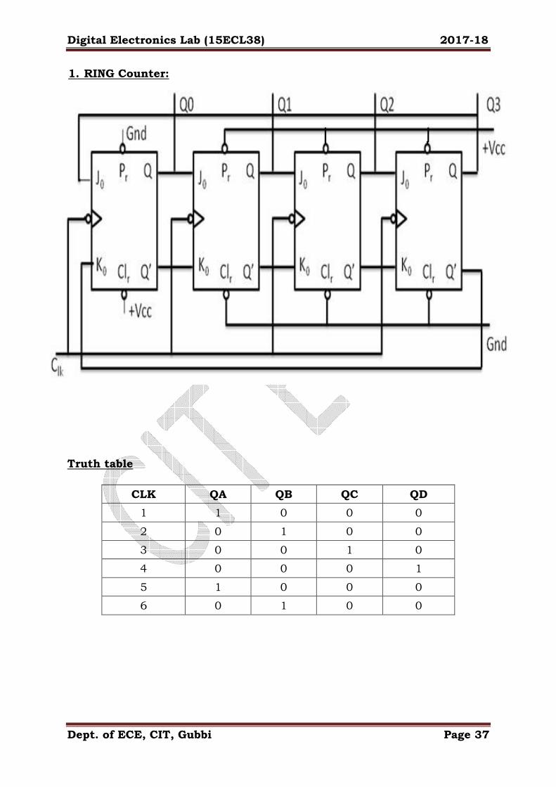
1. RING Counter:
Truth table
CLK QA QB QC QD
1 1 0 0 0
2 0 1 0 0
3 0 0 1 0
4 0 0 0 1
5 1 0 0 0
6 0 1 0 0

Digital Electronics Lab (15ECL38) 2017-18
Dept. of ECE, CIT, Gubbi Page 38
Experiment No: 9 Date:
RING & JHONSON COUNTER USING IC 7476 Aim: To design and study the operation of a ring counter and a Johnson
Counter. Components required: IC 7476, Patch Cards & IC Trainer Kit. Theory:
A ring counter is a circular shift register which is initiated such that
only one of its flip-flops is the state one while others are in their zero states. A ring counter is a Shift Register with the output of the last one connected
to the input of the first, that is, in a ring. Typically, a pattern consisting of a
single bit is circulated so the state repeats every n clock cycles if n flip-flops
are used. It can be used as a cycle counter of n states.
A Johnson counter (or switchtail ring counter, twisted-ring counter,
walking-ring counter, or Moebius counter) is a modified ring counter, where
the output from the last stage is inverted and fed back as input to the first
stage. The register cycles through a sequence of bit-patterns, whose length
is equal to twice the length of the shift register, continuing indefinitely.
These counters find specialist applications, including those similar to the
decade counter, digital-to-analog conversion, etc. They can be implemented
easily using D- or JK-type flip-flops. Procedure: 1. Make the connections as shown in the respective circuit diagram.
2. Initial condition is set by setting up the circuit as shown in the figure.
3. There after all Pr and Clr pins of all F/Fs should be connected to VCC.
4. Apply clock and observe the output after each clock pulse, record the
observations and verify that they match the expected outputs from the
truth table.
5. Repeat the same procedure as above for the Johnson Counter circuit and
verify its operation
Digital Electronics Lab (15ECL38)
Dept. of ECE, CIT, Gubbi
2. JHONSON Counter: Truth table
CLK
1
2
3
4
5
6
7
8
9
10
Digital Electronics Lab (15ECL38)
Dept. of ECE, CIT, Gubbi
QA QB QC
1 0 0
1 1 0
1 1 1
1 1 1
0 1 1
0 0 1
0 0 0
0 0 0
1 0 0
1 1 0
2017-18
Page 39
QD
0
0
0
1
1
1
1
0
0
0

Digital Electronics Lab (15ECL38) 2017-18
Dept. of ECE, CIT, Gubbi Page 40
Result:
Digital Electronics Lab (15ECL38)
Dept. of ECE, CIT, Gubbi
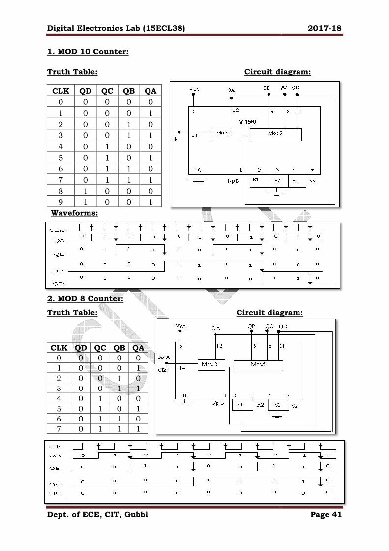
1. MOD 10 Counter: Truth Table:
CLK QD QC QB
0 0 0 0
1 0 0 0
2 0 0 1
3 0 0 1
4 0 1 0
5 0 1 0
6 0 1 1
7 0 1 1
8 1 0 0
9 1 0 0
Waveforms:
2. MOD 8 Counter: Truth Table:
CLK QD QC QB QA
0 0 0 0 0
1 0 0 0 1
2 0 0 1 0
3 0 0 1 1
4 0 1 0 0
5 0 1 0 1
6 0 1 1 0
7 0 1 1 1
Digital Electronics Lab (15ECL38)
Dept. of ECE, CIT, Gubbi
Circuit diagram:
QA
0
1
0
1
0
1
0
1
0
1
Circuit diagram:
QA
2017-18
Page 41
Circuit diagram:
Circuit diagram:
Digital Electronics Lab (15ECL38) 2017-18
Dept. of ECE, CIT, Gubbi Page 42
Experiment No: 10 Date:
DECADE COUNTERS
Aim: To rig up Mod N counter using IC 7490.
Components required: IC7490,Patch cards, trainer kit ,etc.
Procedure:
1. Check all the components for their working.
2. Make connections as shown in the circuit diagram.
3. Clock pulses are applied one by one at the clock input and output is
observed at QA,QB ,QC and QD 4. Verify the Truth Table and observe the outputs.
Result:
Digital Electronics Lab (15ECL38) 2017-18
Dept. of ECE, CIT, Gubbi Page 43
Simulation of Full Adder
Circuit Diagram:
Truth Table:
A B Cin S C
0 0 0 0 0
0 0 1 1 0 S = A ⊕⊕⊕⊕ B ⊕⊕⊕⊕ Cin
0 1 0 1 0 C = A.B + Cin (A ⊕⊕⊕⊕ B)
0 1 1 0 1
1 0 0 1 0
1 0 1 0 1
1 1 0 0 1
1 1 1 1 1

Digital Electronics Lab (15ECL38) 2017-18
Dept. of ECE, CIT, Gubbi Page 44
Experiment No: 11 Date:
FULL ADDER USING SIMULATION TOOL
Aim: To rig up a full adder circuit using basic gates
Procedure to enter schematic and to simulate:
1. Switch on the computer and open the simulation software.
2. Select new file to draw the circuit diagram
3. Select the required components to the circuits from the library and
place them on the window in required position
4. Wire the circuit according to the circuit diagram.
5. Connect the power supply and ground.
6. Save the circuit diagram with file name.
7. Click on simulation button and observe the led on and off condition
and compare with truth table.
Result:
Digital Electronics Lab (15ECL38)
Dept. of ECE, CIT, Gubbi
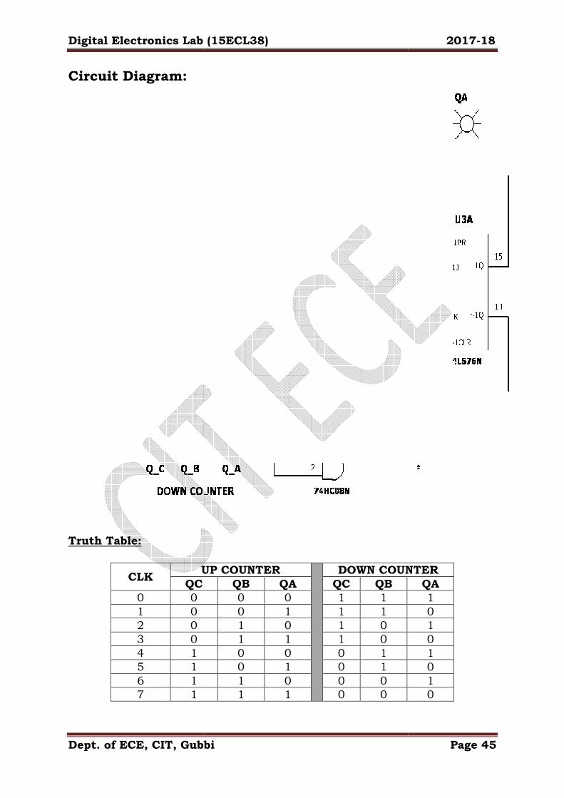
Circuit Diagram: Truth Table:
CLK UP COUNTER
QC
0 0
1 0
2 0
3 0
4 1
5 1
6 1
7 1
Digital Electronics Lab (15ECL38)
Dept. of ECE, CIT, Gubbi
UP COUNTER
DOWN COUNTER
QB QA QC QB
0 0 1 1
0 1 1 1
1 0 1 0
1 1 1 0
0 0 0 1
0 1 0 1
1 0 0 0
1 1 0 0
2017-18
Page 45
DOWN COUNTER
QA
1
0
1
0
1
0
1
0

Digital Electronics Lab (15ECL38) 2017-18
Dept. of ECE, CIT, Gubbi Page 46
Experiment No: 12 Date:
MOD 8 SYNCHRONOUS UP/DOWN COUNTER
USING SIMULATION TOOL Aim: To rig up mod 8 synchronous up/down counter using simulation tool
Procedure to enter schematic and to simulate:
1. Switch on the computer and select Simulation and software.
2. Select new file to draw the circuit diagram
3. Select the required components to the circuits from the library and
place them on the window in required position
4. Wire the circuit according to the circuit diagram.
5. Connect the power supply, clock and ground.
6. Save the circuit diagram with file name.
7. Click on simulation button and observe the led on and off condition
and compare with truth table.
Result:

Digital Electronics Lab (15ECL38) 2017-18
Dept. of ECE, CIT, Gubbi Page 47
IC PIN DETAILS
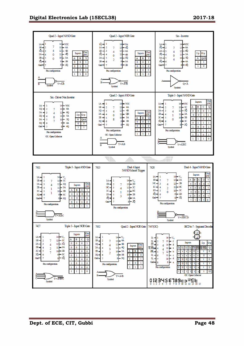
Digital Electronics Lab (15ECL38) 2017-18
Dept. of ECE, CIT, Gubbi Page 48
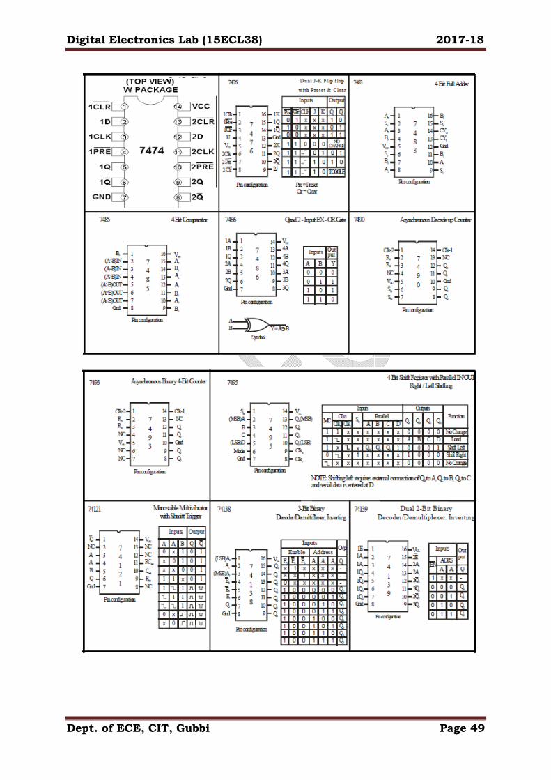
Digital Electronics Lab (15ECL38) 2017-18
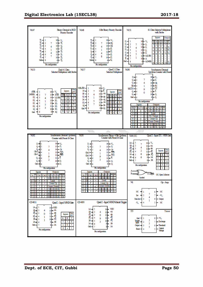
Dept. of ECE, CIT, Gubbi Page 49
Digital Electronics Lab (15ECL38) 2017-18
Dept. of ECE, CIT, Gubbi Page 50
Digital Electronics Lab (15ECL38) 2017-18
Dept. of ECE, CIT, Gubbi Page 51
VIVA QUESTIONS
1. What are Analog Systems? Give Examples. 2. What are Digital Systems? Give Examples. 3. Mention the disadvantages of Analog systems over Digital systems. 4. Explain Boolean algebra. 5. State Principle of Duality. 6. State De – morgan’s Law. 7. Define Positive Logic and Negative Logic. 8. Define Literal. 9. Define MINTERM and MAX TERM. 10. Define a complementary function. 11. Explain Shannon’s reduction theorem. 12. Which are the basic gates and universal gates. 13. Define combinational network with example. 14. Define Sequential Network with example. 15. Define Double-Rail and Single -Rail logic. 16. When a Boolean Expression is called completely specified? 17. Explain the significance of a Don’t care function. 18. Explain the criteria of minimality. 19. Define implies, Subsumes, implicants. 20. What are Prime Implicants? 21. What is irredundant disjunctive normal formula? 22. What is an implicate? 23. What is a Map?

Digital Electronics Lab (15ECL38) 2017-18
Dept. of ECE, CIT, Gubbi Page 52
24. Explain the significance of Map. 25. What is a Minimal Sum and Minimal product? 26. Explain Quine - McClusky method. 27. Explain VEM method of reduction. 28. Explain Binary Adder and Subtractor. 29. Explain various scales of integration. 30. Define Carry Look Ahead Adder. 31. Define Comparator, Decoder and Encoder. 32. Give an example for Min-term generator. 33. Give an example for Max-term generator. 34. Define priority encoder. 35. Explain Multiplexing action. 36. Define PAL, PLA and PROM. 37. Differentiate between ROM and RAM. 38. What is a Memory? 39. What is internal state and secondary state? 40. Define Flip Flop and Latch. 41. Explain Basic Bi-stable element. 42. What is a metastable state? 43. Define setting and clearing in terms of flip-flop. 44. Explain SR Latch and Give an application. 45. Explain gated SR Latch and gated D Latch. 46. Explain Timing Diagram. 47. Explain Propagation Delay in gates. 48. Explain Set and Hold time in latches.
Digital Electronics Lab (15ECL38) 2017-18
Dept. of ECE, CIT, Gubbi Page 53
49. Explain Master-Slave Flip-Flop. 50. Explain the significance of edge-triggering. 51. Explain Data Lock Out. 52. Give the characteristic equations of JK, D and T Flip Flops. 53. Define Registers with example. 54. Define Counters with example. 55. Explain ripple, asynchronous and synchronous counters. 56. Explain Race Around Condition. 57. List the basic logic series. 58. Explain Semiconductor diode behavior. 59. What is Saturating Logic? 60. Explain Fan-Out and Fan-in in gates. 61. Explain DTL and TTL. 62. What is wired logic? 63. What is Totem pole Output? 64. Explain Schottky TTL. 65. Explain Emitter-Coupled Logic. 66. Which is the fastest of all the logic families? 67. What is a MOSFET? 68. Explain Enhancement and Depletion Mode in MOSFET‟s. 69. Explain Threshold voltage. 70. Explain MOSFET as Resistor. 71. Clearly differentiate between PMOS and NMOS Logic. 72. Explain CMOS Logic. 73. State Moore’s Law.
Digital Electronics Lab (15ECL38) 2017-18
Dept. of ECE, CIT, Gubbi Page 54
74. Differentiate between Moore and Mealy Law. 75. Define FPGA. 76. Define PLD. 77. Define CPLD. 78. Define Simulation. 79. State the application of Sequence Generator.

Digital Electronics Lab (15ECL38) 2017-18
Dept. of ECE, CIT, Gubbi Page 55
Question Bank
1. Simplify and realize Demorgan’s theorem for 2 variables. 2. Simplify and realize the given Boolean Expression using Universal
Gates and verify the truth table. (Two expressions to be given).
3. Realize and verify the truth table of full adder basic gates only.
4. Realize and verify the truth table of a full Subtractor using basic gates only.
5. Conduct a suitable experiment on 7483 IC to realize the following
operation on the given 4 bit data addition and subtraction.
6. Realize and verify 4 bit magnitude comparator using IC 7485
7. Realize 4:1 Multiplexer using gates only
8. Realize 3-Variable function using IC 74151(8:1 MUX)
9. Realize and verify 1:8 DEMUX and 3:8 decoder using IC 74138
10. Realize and verify the truth Table of JK Flip Flop using NAND gates
11. Realize and verify the truth Table of Clocked SR Flip Flop using NAND gates
12. Realize and verify Ring counter using IC 7476
13. Realize and verify Johnson counter using IC 7476
14. Realize a Modulo N counter using 7490, Write down the expected
functional table and verify its truth table and also display the waveform.
15. Use IC 7474 Shift registers to display the following operations
a) SIPO b) PIPO
16. Use IC 7474 Shift registers to display the following operations a) PISO b) SISO
17. Simulate full adder using simulation tool
18. Simulate MOD 8 Synchronous up / down counter using simulation tool
----------------------------------*****------------------------------