Embed Size (px)
Citation preview

DDR4 SDRAM RDIMMMTA9ASF51272PZ – 4GB
Features• DDR4 functionality and operations supported as
defined in the component data sheet• 288-pin, registered dual in-line memory module
(RDIMM)• Fast data transfer rates: PC4-2666 or PC4-2400• 4GB (512 Meg x 72)• VDD = 1.20V (NOM)• VPP = 2.5V (NOM)• VDDSPD = 2.5V (NOM)• Supports ECC error detection and correction• Nominal and dynamic on-die termination (ODT) for
data, strobe, and mask signals• Low-power auto self refresh (LPASR)• Data bus inversion (DBI) for data bus• On-die VREFDQ generation and calibration• Single-rank• On-board I2C temperature sensor with integrated
serial presence-detect (SPD) EEPROM• 16 internal banks; 4 groups of 4 banks each• Fixed burst chop (BC) of 4 and burst length (BL) of 8
via the mode register set (MRS)• Selectable BC4 or BL8 on-the-fly (OTF)• Gold edge contacts• Halogen-free• Fly-by topology• Terminated control, command, and address bus
Figure 1: 288-Pin RDIMM (MO-309, R/C-D1)
Module height: 31.25mm (1.23in)
Options Marking• Operating temperature
– Commercial (0°C ≤ TOPER ≤ +95°C) None• Package
– 288-pin DIMM (halogen-free) Z• Frequency/CAS latency
– 0.75ns @ CL = 19 (DDR4-2666) -2G6– 0.83ns @ CL = 17 (DDR4-2400) -2G3
Table 1: Key Timing Parameters
SpeedGrade
IndustryNomen-clature
Data Rate (MT/s)
tRCD(ns)
tRP(ns)
tRC(ns)
CL =20,CL =19
CL =18
CL =17
CL =16
CL =15
CL =14
CL =13
CL =12
CL =11
CL =10
CL =9
-2G6 PC4-2666 2666 2400 2400 2133 2133 1866 1866 1600 1600 1333 – 14.16 14.16 46.16
-2G3 PC4-2400 – 2400 2400 2133 2133 1866 1866 1600 1600 1333 – 14.16 14.16 46.16
-2G1 PC4-2133 – – – 2133 2133 1866 1866 1600 1600 1333 1333 13.5 13.5 46.5
4GB (x72, ECC, SR) 288-Pin DDR4 RDIMMFeatures
CCMTD-1725822587-9516asf9c512x72pz.pdf - Rev. I 5/18 EN 1 Micron Technology, Inc. reserves the right to change products or specifications without notice.
© 2013 Micron Technology, Inc. All rights reserved.
Products and specifications discussed herein are subject to change by Micron without notice.

Table 2: Addressing
Parameter 4GB
Row address 32K A[14:0]
Column address 1K A[9:0]
Device bank group address 4 BG[1:0]
Device bank address per group 4 BA[1:0]
Device configuration 4Gb (512 Meg x 8), 16 banks
Module rank address 1 CS0_n
Table 3: Part Numbers and Timing Parameters – 4GB Modules
Base device: MT40A512M8,1 4Gb DDR4 SDRAM
Part Number2ModuleDensity Configuration
ModuleBandwidth
Memory Clock/Data Rate
Clock Cycles(CL-tRCD-tRP)
MTA9ASF51272PZ-2G6__ 4GB 512 Meg x 72 21.3 GB/s 0.75ns/2666 MT/s 19-19-19
MTA9ASF51272PZ-2G3__ 4GB 512 Meg x 72 19.2 GB/s 0.83ns/2400 MT/s 17-17-17
Notes: 1. The data sheet for the base device can be found on micron.com.2. All part numbers end with a two-place code (not shown) that designates component and PCB revisions.
Consult factory for current revision codes. Example: MTA9ASF51272PZ-2G6F1.
4GB (x72, ECC, SR) 288-Pin DDR4 RDIMMFeatures
CCMTD-1725822587-9516asf9c512x72pz.pdf - Rev. I 5/18 EN 2 Micron Technology, Inc. reserves the right to change products or specifications without notice.
© 2013 Micron Technology, Inc. All rights reserved.

Important Notes and WarningsMicron Technology, Inc. ("Micron") reserves the right to make changes to information published in this document,including without limitation specifications and product descriptions. This document supersedes and replaces allinformation supplied prior to the publication hereof. You may not rely on any information set forth in this docu-ment if you obtain the product described herein from any unauthorized distributor or other source not authorizedby Micron.
Automotive Applications. Products are not designed or intended for use in automotive applications unless specifi-cally designated by Micron as automotive-grade by their respective data sheets. Distributor and customer/distrib-utor shall assume the sole risk and liability for and shall indemnify and hold Micron harmless against all claims,costs, damages, and expenses and reasonable attorneys' fees arising out of, directly or indirectly, any claim ofproduct liability, personal injury, death, or property damage resulting directly or indirectly from any use of non-automotive-grade products in automotive applications. Customer/distributor shall ensure that the terms and con-ditions of sale between customer/distributor and any customer of distributor/customer (1) state that Micronproducts are not designed or intended for use in automotive applications unless specifically designated by Micronas automotive-grade by their respective data sheets and (2) require such customer of distributor/customer to in-demnify and hold Micron harmless against all claims, costs, damages, and expenses and reasonable attorneys'fees arising out of, directly or indirectly, any claim of product liability, personal injury, death, or property damageresulting from any use of non-automotive-grade products in automotive applications.
Critical Applications. Products are not authorized for use in applications in which failure of the Micron compo-nent could result, directly or indirectly in death, personal injury, or severe property or environmental damage("Critical Applications"). Customer must protect against death, personal injury, and severe property and environ-mental damage by incorporating safety design measures into customer's applications to ensure that failure of theMicron component will not result in such harms. Should customer or distributor purchase, use, or sell any Microncomponent for any critical application, customer and distributor shall indemnify and hold harmless Micron andits subsidiaries, subcontractors, and affiliates and the directors, officers, and employees of each against all claims,costs, damages, and expenses and reasonable attorneys' fees arising out of, directly or indirectly, any claim ofproduct liability, personal injury, or death arising in any way out of such critical application, whether or not Mi-cron or its subsidiaries, subcontractors, or affiliates were negligent in the design, manufacture, or warning of theMicron product.
Customer Responsibility. Customers are responsible for the design, manufacture, and operation of their systems,applications, and products using Micron products. ALL SEMICONDUCTOR PRODUCTS HAVE INHERENT FAIL-URE RATES AND LIMITED USEFUL LIVES. IT IS THE CUSTOMER'S SOLE RESPONSIBILITY TO DETERMINEWHETHER THE MICRON PRODUCT IS SUITABLE AND FIT FOR THE CUSTOMER'S SYSTEM, APPLICATION, ORPRODUCT. Customers must ensure that adequate design, manufacturing, and operating safeguards are includedin customer's applications and products to eliminate the risk that personal injury, death, or severe property or en-vironmental damages will result from failure of any semiconductor component.
Limited Warranty. In no event shall Micron be liable for any indirect, incidental, punitive, special or consequentialdamages (including without limitation lost profits, lost savings, business interruption, costs related to the removalor replacement of any products or rework charges) whether or not such damages are based on tort, warranty,breach of contract or other legal theory, unless explicitly stated in a written agreement executed by Micron's dulyauthorized representative.
4GB (x72, ECC, SR) 288-Pin DDR4 RDIMMImportant Notes and Warnings
CCMTD-1725822587-9516asf9c512x72pz.pdf - Rev. I 5/18 EN 3 Micron Technology, Inc. reserves the right to change products or specifications without notice.
© 2013 Micron Technology, Inc. All rights reserved.

Pin AssignmentsThe pin assignment table below is a comprehensive list of all possible pin assignmentsfor DDR4 RDIMM modules. See the Functional Block Diagram for pins specific to thismodule.
Table 4: Pin Assignments
288-Pin DDR4 RDIMM Front 288-Pin DDR4 RDIMM Back
Pin Symbol Pin Symbol Pin Symbol Pin Symbol Pin Symbol Pin Symbol Pin Symbol Pin Symbol
1 NC 37 VSS 73 VDD 109 VSS 145 NC 181 DQ29 217 VDD 253 DQ41
2 VSS 38 DQ24 74 CK0_t 110 DQS14_t/TDQS14_t
146 VREFCA 182 VSS 218 CK1_t 254 VSS
3 DQ4 39 VSS 75 CK0_c 111 DQS14_c/TDQS14_c
147 VSS 183 DQ25 219 CK1_c 255 DQS5_c
4 VSS 40 DQS12_t/TDQS12_t
76 VDD 112 VSS 148 DQ5 184 VSS 220 VDD 256 DQS5_t
5 DQ0 41 DQS12_c/TDQS12_c
77 VTT 113 DQ46 149 VSS 185 DQS3_c 221 VTT 257 VSS
6 VSS 42 VSS 78 EVENT_n 114 VSS 150 DQ1 186 DQS3_t 222 PARITY 258 DQ47
7 DQS9_t/TDQS9_t
43 DQ30 79 A0 115 DQ42 151 VSS 187 VSS 223 VDD 259 VSS
8 DQS09_c/TDQS9_c
44 VSS 80 VDD 116 VSS 152 DQS0_c 188 DQ31 224 BA1 260 DQ43
9 VSS 45 DQ26 81 BA0 117 DQ52 153 DQS0_t 189 VSS 225 A10/AP
261 VSS
10 DQ6 46 VSS 82 RAS_n/A16
118 VSS 154 VSS 190 DQ27 226 VDD 262 DQ53
11 VSS 47 CB4 83 VDD 119 DQ48 155 DQ7 191 VSS 227 NC 263 VSS
12 DQ2 48 VSS 84 CS0_n 120 VSS 156 VSS 192 CB5 228 WE_n/A14
264 DQ49
13 VSS 49 CB0 85 VDD 121 DQS15_t/TDQS15_t
157 DQ3 193 VSS 229 VDD 265 VSS
14 DQ12 50 VSS 86 CAS_n/A15
122 DQS15_c/TDQS15_c
158 VSS 194 CB1 230 NC 266 DQS6_c
15 VSS 51 DQS17_t/TDQS17_t
87 ODT0 123 VSS 159 DQ13 195 VSS 231 VDD 267 DQS6_t
16 DQ8 52 DQS17_c/TDQS17_c
88 VDD 124 DQ54 160 VSS 196 DQS8_c 232 A13 268 VSS
17 VSS 53 VSS 89 CS1_n/NC
125 VSS 161 DQ9 197 DQS8_t 233 VDD 269 DQ55
18 DQS10_t/TDQS10_t
54 CB6 90 VDD 126 DQ50 162 VSS 198 VSS 234 A17 270 VSS
19 DQS10_c/TDQS10_c
55 VSS 91 ODT1/NC
127 VSS 163 DQS1_c 199 CB7 235 NC/C2
271 DQ51
20 VSS 56 CB2 92 VDD 128 DQ60 164 DQS1_t 200 VSS 236 VDD 272 VSS
21 DQ14 57 VSS 93 CS2_n/C0
129 VSS 165 VSS 201 CB3 237 CS3_n/C1, NC
273 DQ61
22 VSS 58 RESET_n 94 VSS 130 DQ56 166 DQ15 202 VSS 238 SA2 274 VSS
23 DQ10 59 VDD 95 DQ36 131 VSS 167 VSS 203 CKE1/NC
239 VSS 275 DQ57
24 VSS 60 CKE0 96 VSS 132 DQS16_t/TDQS16_t
168 DQ11 204 VDD 240 DQ37 276 VSS
4GB (x72, ECC, SR) 288-Pin DDR4 RDIMMPin Assignments
CCMTD-1725822587-9516asf9c512x72pz.pdf - Rev. I 5/18 EN 4 Micron Technology, Inc. reserves the right to change products or specifications without notice.
© 2013 Micron Technology, Inc. All rights reserved.
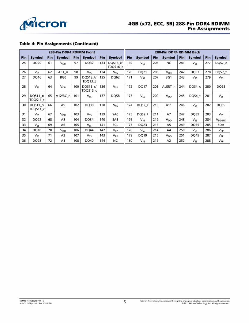
Table 4: Pin Assignments (Continued)
288-Pin DDR4 RDIMM Front 288-Pin DDR4 RDIMM Back
Pin Symbol Pin Symbol Pin Symbol Pin Symbol Pin Symbol Pin Symbol Pin Symbol Pin Symbol
25 DQ20 61 VDD 97 DQ32 133 DQS16_c/TDQS16_c
169 VSS 205 NC 241 VSS 277 DQS7_c
26 VSS 62 ACT_n 98 VSS 134 VSS 170 DQ21 206 VDD 242 DQ33 278 DQS7_t
27 DQ16 63 BG0 99 DQS13_t/TDQ13_t
135 DQ62 171 VSS 207 BG1 243 VSS 279 VSS
28 VSS 64 VDD 100 DQS13_c/TDQS13_c
136 VSS 172 DQ17 208 ALERT_n 244 DQS4_c 280 DQ63
29 DQS11_t/TDQS11_t
65 A12/BC_n 101 VSS 137 DQ58 173 VSS 209 VDD 245 DQS4_t 281 VSS
30 DQS11_c/TDQS11_c
66 A9 102 DQ38 138 VSS 174 DQS2_c 210 A11 246 VSS 282 DQ59
31 VSS 67 VDD 103 VSS 139 SA0 175 DQS2_t 211 A7 247 DQ39 283 VSS
32 DQ22 68 A8 104 DQ34 140 SA1 176 VSS 212 VDD 248 VSS 284 VDDSPD
33 VSS 69 A6 105 VSS 141 SCL 177 DQ23 213 A5 249 DQ35 285 SDA
34 DQ18 70 VDD 106 DQ44 142 VPP 178 VSS 214 A4 250 VSS 286 VPP
35 VSS 71 A3 107 VSS 143 VPP 179 DQ19 215 VDD 251 DQ45 287 VPP
36 DQ28 72 A1 108 DQ40 144 NC 180 VSS 216 A2 252 VSS 288 VPP
4GB (x72, ECC, SR) 288-Pin DDR4 RDIMMPin Assignments
CCMTD-1725822587-9516asf9c512x72pz.pdf - Rev. I 5/18 EN 5 Micron Technology, Inc. reserves the right to change products or specifications without notice.
© 2013 Micron Technology, Inc. All rights reserved.

Pin DescriptionsThe pin description table below is a comprehensive list of all possible pins for DDR4modules. All pins listed may not be supported on this module. See Functional Block Di-agram for pins specific to this module.
Table 5: Pin Descriptions
Symbol Type Description
Ax Input Address inputs: Provide the row address for ACTIVATE commands and the column address forREAD/WRITE commands in order to select one location out of the memory array in the respec-tive bank (A10/AP, A12/BC_n, WE_n/A14, CAS_n/A15, and RAS_n/A16 have additional functions;see individual entries in this table). The address inputs also provide the op-code during theMODE REGISTER SET command. A17 is only defined for x4 SDRAM.
A10/AP Input Auto precharge: A10 is sampled during READ and WRITE commands to determine whether anauto precharge should be performed on the accessed bank after a READ or WRITE operation(HIGH = auto precharge; LOW = no auto precharge). A10 is sampled during a PRECHARGE com-mand to determine whether the precharge applies to one bank (A10 LOW) or all banks (A10HIGH). If only one bank is to be precharged, the bank is selected by the bank group and bankaddresses.
A12/BC_n Input Burst chop: A12/BC_n is sampled during READ and WRITE commands to determine if burstchop (on-the-fly) will be performed (HIGH = no burst chop; LOW = burst chopped). See Com-mand Truth Table in the DDR4 component data sheet.
ACT_n Input Command input: ACT_n defines the ACTIVATE command being entered along with CS_n. Theinput into RAS_n/A16, CAS_n/A15, and WE_n/A14 are considered as row address A16, A15, andA14. See Command Truth Table.
BAx Input Bank address inputs: Define the bank (with a bank group) to which an ACTIVATE, READ,WRITE, or PRECHARGE command is being applied. Also determine which mode register is to beaccessed during a MODE REGISTER SET command.
BGx Input Bank group address inputs: Define the bank group to which a REFRESH, ACTIVATE, READ,WRITE, or PRECHARGE command is being applied. Also determine which mode register is to beaccessed during a MODE REGISTER SET command. BG[1:0] are used in the x4 and x8 configura-tions. x16-based SDRAM only has BG0.
C0, C1, C2(RDIMM/LRDIMM on-
ly)
Input Chip ID: These inputs are used only when devices are stacked; that is, 2H, 4H, and 8H stacks forx4 and x8 configurations using through-silicon vias (TSVs). These pins are not used in the x16configuration. Some DDR4 modules support a traditional DDP package, which uses CS1_n,CKE1, and ODT1 to control the second die. All other stack configurations, such as a 4H or 8H,are assumed to be single-load (master/slave) type configurations where C0, C1, and C2 are usedas chip ID selects in conjunction with a single CS_n, CKE, and ODT. Chip ID is considered part ofthe command code.
CKx_tCKx_c
Input Clock: Differential clock inputs. All address, command, and control input signals are sampledon the crossing of the positive edge of CK_t and the negative edge of CK_c.
CKEx Input Clock enable: CKE HIGH activates and CKE LOW deactivates the internal clock signals, deviceinput buffers, and output drivers. Taking CKE LOW provides PRECHARGE POWER-DOWN andSELF REFRESH operations (all banks idle), or active power-down (row active in any bank). CKE isasynchronous for self refresh exit. After VREFCA has become stable during the power-on and ini-tialization sequence, it must be maintained during all operations (including SELF REFRESH). CKEmust be maintained HIGH throughout read and write accesses. Input buffers (excluding CK_t,CK_c, ODT, RESET_n, and CKE) are disabled during power-down. Input buffers (excluding CKEand RESET_n) are disabled during self refresh.
CSx_n Input Chip select: All commands are masked when CS_n is registered HIGH. CS_n provides externalrank selection on systems with multiple ranks. CS_n is considered part of the command code(CS2_n and CS3_n are not used on UDIMMs).
4GB (x72, ECC, SR) 288-Pin DDR4 RDIMMPin Descriptions
CCMTD-1725822587-9516asf9c512x72pz.pdf - Rev. I 5/18 EN 6 Micron Technology, Inc. reserves the right to change products or specifications without notice.
© 2013 Micron Technology, Inc. All rights reserved.

Table 5: Pin Descriptions (Continued)
Symbol Type Description
ODTx Input On-die termination: ODT (registered HIGH) enables termination resistance internal to theDDR4 SDRAM. When enabled, ODT (RTT) is applied only to each DQ, DQS_t, DQS_c, DM_n/DBI_n/TDQS_t, and TDQS_c signal for x4 and x8 configurations (when the TDQS function is ena-bled via the mode register). For the x16 configuration, RTT is applied to each DQ, DQSU_t,DQSU_c, DQSL_t, DQSL_c, UDM_n, and LDM_n signal. The ODT pin will be ignored if the moderegisters are programmed to disable RTT.
PARITY Input Parity for command and address: This function can be enabled or disabled via the moderegister. When enabled in MR5, the DRAM calculates parity with ACT_n, RAS_n/A16, CAS_n/A15,WE_n/A14, BG[1:0], BA[1:0], A[16:0]. Input parity should be maintained at the rising edge of theclock and at the same time as command and address with CS_n LOW.
RAS_n/A16CAS_n/A15WE_n/A14
Input Command inputs: RAS_n/A16, CAS_n/A15, and WE_n/A14 (along with CS_n) define the com-mand and/or address being entered and have multiple functions. For example, for activationwith ACT_n LOW, these are addresses like A16, A15, and A14, but for a non-activation com-mand with ACT_n HIGH, these are command pins for READ, WRITE, and other commands de-fined in Command Truth Table.
RESET_n CMOS Input Active LOW asynchronous reset: Reset is active when RESET_n is LOW and inactive when RE-SET_n is HIGH. RESET_n must be HIGH during normal operation.
SAx InputSerial address inputs: Used to configure the temperature sensor/SPD EEPROM address rangeon the I2C bus.
SCL InputSerial clock for temperature sensor/SPD EEPROM: Used to synchronize communication toand from the temperature sensor/SPD EEPROM on the I2C bus.
DQx, CBx I/O Data input/output and check bit input/output: Bidirectional data bus. DQ representsDQ[3:0], DQ[7:0], and DQ[15:0] for the x4, x8, and x16 configurations, respectively. If cyclic re-dundancy checksum (CRC) is enabled via the mode register, the CRC code is added at the end ofthe data burst. Any one or all of DQ0, DQ1, DQ2, or DQ3 may be used for monitoring of inter-nal VREF level during test via mode register setting MR[4] A[4] = HIGH; training times changewhen enabled.
DM_n/DBI_n/TDQS_t (DMU_n,DBIU_n), (DML_n/
DBIl_n)
I/O Input data mask and data bus inversion: DM_n is an input mask signal for write data. Inputdata is masked when DM_n is sampled LOW coincident with that input data during a write ac-cess. DM_n is sampled on both edges of DQS. DM is multiplexed with the DBI function by themode register A10, A11, and A12 settings in MR5. For a x8 device, the function of DM or TDQSis enabled by the mode register A11 setting in MR1. DBI_n is an input/output identifyingwhether to store/output the true or inverted data. If DBI_n is LOW, the data will be stored/output after inversion inside the DDR4 device and not inverted if DBI_n is HIGH. TDQS is onlysupported in x8 SDRAM configurations (TDQS is not valid for UDIMMs).
SDA I/O Serial Data: Bidirectional signal used to transfer data in or out of the EEPROM or EEPROM/TScombo device.
DQS_tDQS_c
DQSU_tDQSU_cDQSL_tDQSL_c
I/O Data strobe: Output with read data, input with write data. Edge-aligned with read data, cen-tered-aligned with write data. For x16 configurations, DQSL corresponds to the data onDQ[7:0], and DQSU corresponds to the data on DQ[15:8]. For the x4 and x8 configurations, DQScorresponds to the data on DQ[3:0] and DQ[7:0], respectively. DDR4 SDRAM supports a differen-tial data strobe only and does not support a single-ended data strobe.
ALERT_n Output Alert output: Possesses functions such as CRC error flag and command and address parity errorflag as output signal. If a CRC error occurs, ALERT_n goes LOW for the period time interval andreturns HIGH. If an error occurs during a command address parity check, ALERT_n goes LOW un-til the on-going DRAM internal recovery transaction is complete. During connectivity test mode,this pin functions as an input. Use of this signal is system-dependent. If not connected as signal,ALERT_n pin must be connected to VDD on DIMMs.
EVENT_n Output Temperature event: The EVENT_n pin is asserted by the temperature sensor when critical tem-perature thresholds have been exceeded. This pin has no function (NF) on modules withouttemperature sensors.
4GB (x72, ECC, SR) 288-Pin DDR4 RDIMMPin Descriptions
CCMTD-1725822587-9516asf9c512x72pz.pdf - Rev. I 5/18 EN 7 Micron Technology, Inc. reserves the right to change products or specifications without notice.
© 2013 Micron Technology, Inc. All rights reserved.

Table 5: Pin Descriptions (Continued)
Symbol Type Description
TDQS_tTDQS_c
(x8 DRAM-basedRDIMM only)
Output Termination data strobe: When enabled via the mode register, the DRAM device enables thesame RTT termination resistance on TDQS_t and TDQS_c that is applied to DQS_t and DQS_c.When the TDQS function is disabled via the mode register, the DM/TDQS_t pin provides the da-ta mask (DM) function, and the TDQS_c pin is not used. The TDQS function must be disabled inthe mode register for both the x4 and x16 configurations. The DM function is supported only inx8 and x16 configurations. DM, DBI, and TDQS are a shared pin and are enabled/disabled bymode register settings. For more information about TDQS, see the DDR4 DRAM component da-ta sheet (TDQS_t and TDQS_c are not valid for UDIMMs).
VDD Supply Module power supply: 1.2V (TYP).
VPP Supply DRAM activating power supply: 2.5V –0.125V / +0.250V.
VREFCA Supply Reference voltage for control, command, and address pins.
VSS Supply Ground.
VTT Supply Power supply for termination of address, command, and control VDD/2.
VDDSPD Supply Power supply used to power the I2C bus for SPD.
RFU – Reserved for future use.
NC – No connect: No internal electrical connection is present.
NF – No function: May have internal connection present, but has no function.
4GB (x72, ECC, SR) 288-Pin DDR4 RDIMMPin Descriptions
CCMTD-1725822587-9516asf9c512x72pz.pdf - Rev. I 5/18 EN 8 Micron Technology, Inc. reserves the right to change products or specifications without notice.
© 2013 Micron Technology, Inc. All rights reserved.

DQ Map
Table 6: Component-to-Module DQ Map
ComponentReferenceNumber
ComponentDQ Module DQ
Module PinNumber
ComponentReferenceNumber
ComponentDQ Module DQ
Module PinNumber
U1 0 10 23 U2 0 26 45
1 9 161 1 25 183
2 11 168 2 27 190
3 8 16 3 24 38
4 15 166 4 31 188
5 12 14 5 28 36
6 14 21 6 30 43
7 13 159 7 29 181
U5 0 42 115 U6 0 58 137
1 41 253 1 57 275
2 43 260 2 59 282
3 40 108 3 56 130
4 47 258 4 63 280
5 44 106 5 60 128
6 46 113 6 62 135
7 45 251 7 61 273
U7 0 52 117 U8 0 36 95
1 54 124 1 38 102
2 53 262 2 37 240
3 55 267 3 39 247
4 48 119 4 32 97
5 51 271 5 35 249
6 49 264 6 33 242
7 50 126 7 34 104
U9 0 CB4 47 U10 0 20 25
1 CB6 54 1 22 32
2 CB5 192 2 21 170
3 CB7 199 3 23 177
4 CB0 49 4 16 27
5 CB3 201 5 19 179
6 CB1 194 6 17 172
7 CB2 56 7 18 34
4GB (x72, ECC, SR) 288-Pin DDR4 RDIMMDQ Map
CCMTD-1725822587-9516asf9c512x72pz.pdf - Rev. I 5/18 EN 9 Micron Technology, Inc. reserves the right to change products or specifications without notice.
© 2013 Micron Technology, Inc. All rights reserved.

Table 6: Component-to-Module DQ Map (Continued)
ComponentReferenceNumber
ComponentDQ Module DQ
Module PinNumber
ComponentReferenceNumber
ComponentDQ Module DQ
Module PinNumber
U11 0 4 1
1 6 10
2 5 148
3 7 155
4 0 5
5 3 157
6 1 150
7 2 12
4GB (x72, ECC, SR) 288-Pin DDR4 RDIMMDQ Map
CCMTD-1725822587-9516asf9c512x72pz.pdf - Rev. I 5/18 EN 10 Micron Technology, Inc. reserves the right to change products or specifications without notice.
© 2013 Micron Technology, Inc. All rights reserved.

Functional Block Diagram
Figure 2: Functional Block Diagram
DQ DQ DQ DQ DQ DQ DQ DQ ZQ
DQ0 DQ1 DQ2 DQ3 DQ4 DQ5 DQ6 DQ7
U11
DQ32 DQ33 DQ34 DQ35 DQ36 DQ37 DQ38 DQ39
U8
DQ8 DQ9
DQ10 DQ11 DQ12 DQ13 DQ14 DQ15
U1
DQ40 DQ41 DQ42 DQ43 DQ44 DQ45 DQ46 DQ47
U5
DQ16 DQ17 DQ18 DQ19 DQ20 DQ21 DQ22 DQ23
U10
DQ48 DQ49 DQ50 DQ51 DQ52 DQ53 DQ54 DQ55
U7
DQ24 DQ25 DQ26 DQ27 DQ28 DQ29 DQ30 DQ31
U2
DQ56 DQ57 DQ58 DQ59 DQ60 DQ61 DQ62 DQ63
U6
CB0 CB1 CB2 CB3 CB4 CB5 CB6 CB7
U9
DQ DQ DQ DQ DQ DQ DQ DQ ZQ
DQ DQ DQ DQ DQ DQ DQ DQ ZQ
DQ DQ DQ DQ DQ DQ DQ DQ ZQ
DQ DQ DQ DQ DQ DQ DQ DQ ZQ
DQ DQ DQ DQ DQ DQ DQ DQ ZQ
DQ DQ DQ DQ DQ DQ DQ DQ ZQ
DQ DQ DQ DQ DQ DQ DQ DQ ZQ
DQ DQ DQ DQ DQ DQ DQ DQ ZQ
CS0_n
Vss
Vss
Vss
Vss
Vss
Vss
Vss
Vss
Vss
DQS0_t DQS0_c TDQS0_t TDQS0_c
U3
VREFCA
VSS
DDR4 SDRAM, Register
DDR4 SDRAM, Register
VDD
Control, command andaddress termination
VDDSPDSPD EEPROM/Temp Sensor, Register
VTT
DDR4 SDRAM, Register
DDR4 SDRAMVPP
A/B-CS0_n, A/B-BA[1:0]A/B-BG[1:0], A/B-ACT_n, A/B-A[17, 13:0], A/B-RAS_n/A16,
A/B-CAS_n/A15, A/B-WE_n/A14, A/B-CKE0, A/B-ODT0
CK[3:0]_tCK[3:0]_c
Command, control, address, and clock line terminations:
DDR4 SDRAM
VTT
DDR4 SDRAM
VDD
U4
A0
SPD EEPROM/ Temperature
sensorA1 A2
SA0 SA1
SDASCL
EVT
EVENT_n
CS0_n BA[1:0] BG[1:0] ACT_n
A[17, 13:0]RAS_n/A16CAS_n/A15 WE_n/A14
CKE0 ODT0
PAR_IN ALERT_CONN_N
A/B-CS0_n: Rank 0 A/B-BA[1:0]: DDR4 SDRAMs A/B-BG[1:0]: DDR4 SDRAMs A/B-ACT_n: DDR4 SDRAMS A/B-A[17,13:0]: DDR4 SDRAMs A/B-RAS_n/A16: DDR4 SDRAMs A/B-CAS_n/A15: DDR4 SDRAMs A/B-WE_n/A14: DDR4 SDRAMs A/B-CKE0: Rank 0 A/B-ODT0: Rank 0 A/B-PAR: DDR4 SDRAMs ALERT_DRAM: DDR4 SDRAMs
R
E
G
I
S
T
E
R
&
P
L
L
RESET_CONN
CK[1:0]_cDDR4 SDRAMs
RESET_DRAM: DDR4 SDRAMs
CK[1:0]_t
ZQ
VSS
SA2
TDQS_c DM_n/ CS_n DQS_t DQS_c DBI_n/ TDQS_t
TDQS_c DM_n/ CS_n DQS_t DQS_c DBI_n/ TDQS_t
TDQS_c DM_n/ CS_n DQS_t DQS_c DBI_n/ TDQS_t
TDQS_c DM_n/ CS_n DQS_t DQS_c DBI_n/ TDQS_t
TDQS_c DM_n/ CS_n DQS_t DQS_c DBI_n/ TDQS_t
TDQS_c DM_n/ CS_n DQS_t DQS_c DBI_n/ TDQS_t
TDQS_c DM_n/ CS_n DQS_t DQS_c DBI_n/ TDQS_t
TDQS_c DM_n/ CS_n DQS_t DQS_c DBI_n/ TDQS_t
TDQS_c DM_n/ CS_n DQS_t DQS_c DBI_n/ TDQS_t
DQS4_t DQS4_c TDQS4_t TDQS4_c
DQS1_t DQS1_c TDQS1_t TDQS1_c
DQS2_t DQS2_c TDQS2_t TDQS2_c
DQS3_t DQS3_c TDQS3_t TDQS3_c
DQS8_t DQS8_c TDQS8_t TDQS8_c
DQS5_t DQS5_c TDQS5_t TDQS5_c
DQS6_t DQS6_c TDQS6_t TDQS6_c
DQS7_t DQS7_c TDQS7_t TDQS7_c
SA0 SA1 SA2 SCL
SDA
CK0_t CK0_c
CK1_t
CK1_c
Note: 1. The ZQ ball on each DDR4 component is connected to an external 240Ω ±1% resistorthat is tied to ground. It is used for the calibration of the component’s ODT and outputdriver.
4GB (x72, ECC, SR) 288-Pin DDR4 RDIMMFunctional Block Diagram
CCMTD-1725822587-9516asf9c512x72pz.pdf - Rev. I 5/18 EN 11 Micron Technology, Inc. reserves the right to change products or specifications without notice.
© 2013 Micron Technology, Inc. All rights reserved.

General DescriptionHigh-speed DDR4 SDRAM modules use DDR4 SDRAM devices with two or four internalmemory bank groups. DDR4 SDRAM modules utilizing 4- and 8-bit-wide DDR4 SDRAMdevices have four internal bank groups consisting of four memory banks each, provid-ing a total of 16 banks. 16-bit-wide DDR4 SDRAM devices have two internal bankgroups consisting of four memory banks each, providing a total of eight banks. DDR4SDRAM modules benefit from DDR4 SDRAM's use of an 8n-prefetch architecture withan interface designed to transfer two data words per clock cycle at the I/O pins. A singleREAD or WRITE operation for the DDR4 SDRAM effectively consists of a single 8n-bit-wide, four-clock data transfer at the internal DRAM core and eight corresponding n-bit-wide, one-half-clock-cycle data transfers at the I/O pins.
DDR4 modules use two sets of differential signals: DQS_t and DQS_c to capture dataand CK_t and CK_c to capture commands, addresses, and control signals. Differentialclocks and data strobes ensure exceptional noise immunity for these signals and pro-vide precise crossing points to capture input signals.
Fly-By Topology
DDR4 modules use faster clock speeds than earlier DDR technologies, making signalquality more important than ever. For improved signal quality, the clock, control, com-mand, and address buses have been routed in a fly-by topology, where each clock, con-trol, command, and address pin on each DRAM is connected to a single trace and ter-minated (rather than a tree structure, where the termination is off the module near theconnector). Inherent to fly-by topology, the timing skew between the clock and DQS sig-nals can be easily accounted for by using the write-leveling feature of DDR4.
Module Manufacturing Location
Micron Technology manufactures modules at sites world-wide. Customers may receivemodules from any of the following manufacturing locations:
Table 7: DRAM Module Manufacturing Locations
Manufacturing Site Location Country of Origin Specified on Label
Boise, USA USA
Aguadilla, Puerto Rico Puerto Rico
Xian, China China
Singapore Singapore
4GB (x72, ECC, SR) 288-Pin DDR4 RDIMMGeneral Description
CCMTD-1725822587-9516asf9c512x72pz.pdf - Rev. I 5/18 EN 12 Micron Technology, Inc. reserves the right to change products or specifications without notice.
© 2013 Micron Technology, Inc. All rights reserved.

Address Mapping to DRAM
Address Mirroring
To achieve optimum routing of the address bus on DDR4 multi rank modules, the ad-dress bus will be wired as shown in the table below, or mirrored. For quad rank mod-ules, ranks 1 and 3 are mirrored and ranks 0 and 2 are non-mirrored. Highlighted ad-dress pins have no secondary functions allowing for normal operation when cross-wired. Data is still read from the same address it was written. However, Load Mode op-erations require a specific address. This requires the controller to accommodate for arank that is "mirrored." Systems may reference DDR4 SPD to determine if the modulehas mirroring implemented or not. See the JEDEC DDR4 SPD specification for more de-tails.
Table 8: Address Mirroring
Edge Connector Pin DRAM Pin, Non-mirrored DRAM Pin, Mirrored
A0 A0 A0
A1 A1 A1
A2 A2 A2
A3 A3 A4
A4 A4 A3
A5 A5 A6
A6 A6 A5
A7 A7 A8
A8 A8 A7
A9 A9 A9
A10 A10 A10
A11 A11 A13
A13 A13 A11
A12 A12 A12
A14 A14 A14
A15 A15 A15
A16 A16 A16
A17 A17 A17
BA0 BA0 BA1
BA1 BA1 BA0
BG0 BG0 BG1
BG1 BG1 BG0
4GB (x72, ECC, SR) 288-Pin DDR4 RDIMMAddress Mapping to DRAM
CCMTD-1725822587-9516asf9c512x72pz.pdf - Rev. I 5/18 EN 13 Micron Technology, Inc. reserves the right to change products or specifications without notice.
© 2013 Micron Technology, Inc. All rights reserved.

Registering Clock Driver OperationRegistered DDR4 SDRAM modules use a registering clock driver device consisting of aregister and a phase-lock loop (PLL). The device complies with the JEDEC DDR4 RCDspecification.
To reduce the electrical load on the host memory controller's command, address, andcontrol bus, Micron's RDIMMs utilize a DDR4 registering clock driver (RCD). The RCDpresents a single load to the controller while redriving signals to the DDR4 SDRAM de-vices, which helps enable higher densities and increase signal integrity. The RCD alsoprovides a low-jitter, low-skew PLL that redistributes a differential clock pair to multipledifferential pairs of clock outputs.
Control Words
The RCD device(s) used on DDR4 RDIMMs, LRDIMMs, and NVDIMMs contain configu-ration registers known as control words, which the host uses to configure the RCDbased on criteria determined by the module design. Control words can be set by thehost controller through either the DRAM address and control bus or the I2C bus inter-face. The RCD I2C bus interface resides on the same I2C bus interface as the moduletemperature sensor and EEPROM.
Parity Operations
The RCD includes a parity-checking function that can be enabled or disabled in controlword RC0E. The RCD receives a parity bit at the DPAR input from the memory control-ler and compares it with the data received on the qualified command and address in-puts; it indicates on its open-drain ALERT_n pin whether a parity error has occurred. Ifparity checking is enabled, the RCD forwards commands to the SDRAM when no parityerror has occurred. If the parity error function is disabled, the RCD forwards sampledcommands to the SDRAM regardless of whether a parity error has occurred. Parity is al-so checked during control word WRITE operations unless parity checking is disabled.
Rank Addressing
The chip select pins (CS_n) on Micron's modules are used to select a specific rank ofDRAM. The RDIMM is capable of selecting ranks in one of three different operatingmodes, dependant on setting DA[1:0] bits in the DIMM configuration control word lo-cated within the RCD. Direct DualCS mode is utilized for single- or dual-rank modules.For quad-rank modules, either direct or encoded QuadCS mode is used.
4GB (x72, ECC, SR) 288-Pin DDR4 RDIMMRegistering Clock Driver Operation
CCMTD-1725822587-9516asf9c512x72pz.pdf - Rev. I 5/18 EN 14 Micron Technology, Inc. reserves the right to change products or specifications without notice.
© 2013 Micron Technology, Inc. All rights reserved.

Temperature Sensor with SPD EEPROM Operation
Thermal Sensor Operations
The integrated thermal sensor continuously monitors the temperature of the modulePCB directly below the device and updates the temperature data register. Temperaturedata may be read from the bus host at any time, which provides the host real-time feed-back of the module's temperature. Multiple programmable and read-only temperatureregisters can be used to create a custom temperature-sensing solution based on systemrequirements and JEDEC JC-42.2.
EVENT_n Pin
The temperature sensor also adds the EVENT_n pin (open-drain), which requires a pull-up to VDDSPD. EVENT_n is a temperature sensor output used to flag critical events thatcan be set up in the sensor’s configuration registers. EVENT_n is not used by the serialpresence-detect (SPD) EEPROM.
EVENT_n has three defined modes of operation: interrupt, comparator, and TCRIT. Ininterrupt mode, the EVENT_n pin remains asserted until it is released by writing a 1 tothe clear event bit in the status register. In comparator mode, the EVENT_n pin clearsitself when the error condition is removed. Comparator mode is always used when thetemperature is compared against the TCRIT limit. In TCRIT only mode, the EVENT_npin is only asserted if the measured temperature exceeds the TCRIT limit; it then re-mains asserted until the temperature drops below the TCRIT limit minus the TCRIThysteresis.
SPD EEPROM Operation
DDR4 SDRAM modules incorporate SPD. The SPD data is stored in a 512-byte, JEDECJC-42.4-compliant EEPROM that is segregated into four 128-byte, write-protectableblocks. The SPD content is aligned with these blocks as shown in the table below.
Block Range Description
0 0–127 000h–07Fh Configuration and DRAM parameters
1 128–255 080h–0FFh Module parameters
2 256–319 100h–13Fh Reserved (all bytes coded as 00h)
320–383 140h–17Fh Manufacturing information
3 384–511 180h–1FFh End-user programmable
The first 384 bytes are programmed by Micron to comply with JEDEC standard JC-45,"Appendix X: Serial Presence Detect (SPD) for DDR4 SDRAM Modules." The remaining128 bytes of storage are available for use by the customer.
The EEPROM resides on a two-wire I2C serial interface and is not integrated with thememory bus in any manner. It operates as a slave device in the I2C bus protocol, with alloperations synchronized by the serial clock. Transfer rates of up to 1 MHz are achieva-ble at 2.5V (NOM).
Micron implements reversible software write protection on DDR4 SDRAM-based mod-ules. This prevents the lower 384 bytes (bytes 0 to 383) from being inadvertently pro-grammed or corrupted. The upper 128 bytes remain available for customer use and areunprotected.
4GB (x72, ECC, SR) 288-Pin DDR4 RDIMMTemperature Sensor with SPD EEPROM Operation
CCMTD-1725822587-9516asf9c512x72pz.pdf - Rev. I 5/18 EN 15 Micron Technology, Inc. reserves the right to change products or specifications without notice.
© 2013 Micron Technology, Inc. All rights reserved.

Electrical SpecificationsStresses greater than those listed may cause permanent damage to the module. This is astress rating only, and functional operation of the module at these or any other condi-tions outside those indicated in each device's data sheet is not implied. Exposure to ab-solute maximum rating conditions for extended periods may adversely affect reliability.
Table 9: Absolute Maximum Ratings
Symbol Parameter Min Max Units Notes
VDD VDD supply voltage relative to VSS –0.4 1.5 V 1
VDDQ VDDQ supply voltage relative to VSS –0.4 1.5 V 1
VPP Voltage on VPP pin relative to VSS –0.4 3.0 V 2
VIN, VOUT Voltage on any pin relative to VSS –0.4 1.5 V
Table 10: Operating Conditions
Symbol Parameter Min Nom Max Units Notes
VDD VDD supply voltage 1.14 1.20 1.26 V 1
VPP DRAM activating power supply 2.375 2.5 2.75 V 2
VREFCA(DC) Input reference voltage –command/address bus
0.49 × VDD 0.5 × VDD 0.51 × VDD V 3
IVTT Termination reference current from VTT –750 – 750 mA
VTT Termination reference voltage (DC) –command/address bus
0.49 × VDD -20mV
0.5 × VDD 0.51 × VDD +20mV
V 4
IIN Input leakage current; any input excluding ZQ; 0V <VIN < 1.1V
–2 – 2 µA 5
IZQ Input leakage current; ZQ –50 – 10 µA 6, 7
IOZpd Output leakage current; VOUT = VDD; DQ is disabled – – 10 µA
IOZpu Output leakage current; VOUT = VSS; DQ is disabled;ODT is disabled with ODT input HIGH
–50 – – µA
IVREFCA VREFCA leakage; VREFCA = VDD/2 (after DRAM is ini-tialized)
–2 – 2 µA 7
Notes: 1. VDDQ balls on DRAM are tied to VDD.2. VPP must be greater than or equal to VDD at all times.3. VREFCA must not be greater than 0.6 × VDD. When VDD is less than 500mV, VREF may be
less than or equal to 300mV.4. VTT termination voltages in excess of specification limit adversely affect command and
address signals' voltage margins and reduce timing margins.5. Command and address inputs are terminated to VDD/2 in the registering clock driver. In-
put current is dependent on termination resistance set in the registering clock driver.6. Tied to ground. Not connected to edge connector.7. Multiply by number of DRAM die on module.
4GB (x72, ECC, SR) 288-Pin DDR4 RDIMMElectrical Specifications
CCMTD-1725822587-9516asf9c512x72pz.pdf - Rev. I 5/18 EN 16 Micron Technology, Inc. reserves the right to change products or specifications without notice.
© 2013 Micron Technology, Inc. All rights reserved.

Table 11: Thermal Characteristics
Symbol Parameter/Condition Value Units Notes
TC Commercial operating case temperature 0 to 85 °C 1, 2, 3
TC >85 to 95 °C 1, 2, 3, 4
TOPER Normal operating temperature range 0 to 85 °C 5, 7
TOPER Extended temperature operating range (optional) >85 to 95 °C 5, 7
TSTG Non-operating storage temperature –55 to 100 °C 6
RHSTG Non-operating storage relative humidity (non-condensing) 5 to 95 %
NA Change rate of storage temperature 20 °C/hour
Notes: 1. Maximum operating case temperature; TC is measured in the center of the package.2. A thermal solution must be designed to ensure the DRAM device does not exceed the
maximum TC during operation.3. Device functionality is not guaranteed if the DRAM device exceeds the maximum TC dur-
ing operation.4. If TC exceeds 85°C, the DRAM must be refreshed externally at 2X refresh, which is a 3.9µs
interval refresh rate.5. The refresh rate must double when 85°C < TOPER ≤ 95°C.6. Storage temperature is defined as the temperature of the top/center of the DRAM and
does not reflect the storage temperatures of shipping trays.7. For additional information, refer to technical note TN-00-08: "Thermal Applications"
available at micron.com.
4GB (x72, ECC, SR) 288-Pin DDR4 RDIMMElectrical Specifications
CCMTD-1725822587-9516asf9c512x72pz.pdf - Rev. I 5/18 EN 17 Micron Technology, Inc. reserves the right to change products or specifications without notice.
© 2013 Micron Technology, Inc. All rights reserved.

DRAM Operating ConditionsRecommended AC operating conditions are given in the DDR4 component data sheets.Component specifications are available at micron.com. Module speed grades correlatewith component speed grades, as shown below.
Table 12: Module and Component Speed Grades
DDR4 components may exceed the listed module speed grades; module may not be available in all listed speed gradesModule Speed Grade Component Speed Grade
-3G2 -062E
-2G9 -068
-2G6 -075
-2G3 -083
-2G1 -093E
Design Considerations
Simulations
Micron memory modules are designed to optimize signal integrity through carefully de-signed terminations, controlled board impedances, routing topologies, trace lengthmatching, and decoupling. However, good signal integrity starts at the system level. Mi-cron encourages designers to simulate the signal characteristics of the system's memo-ry bus to ensure adequate signal integrity of the entire memory system.
Power
Operating voltages are specified at the edge connector of the module, not at the DRAM.Designers must account for any system voltage drops at anticipated power levels to en-sure the required supply voltage is maintained.
4GB (x72, ECC, SR) 288-Pin DDR4 RDIMMDRAM Operating Conditions
CCMTD-1725822587-9516asf9c512x72pz.pdf - Rev. I 5/18 EN 18 Micron Technology, Inc. reserves the right to change products or specifications without notice.
© 2013 Micron Technology, Inc. All rights reserved.

IDD Specifications
Table 13: DDR4 IDD Specifications and Conditions – 4GB (Die Revision B)
Values are for the MT40A512M8 DDR4 SDRAM only and are computed from values specified in the 4Gb (512 Meg x 8) com-ponent data sheetParameter Symbol 2666 2400 Units
One bank ACTIVATE-PRECHARGE current IDD0 531 504 mA
One bank ACTIVATE-PRECHARGE, word line boost, IPP current IPP0 36 36 mA
One bank ACTIVATE-READ-PRECHARGE current IDD1 684 657 mA
Precharge standby current IDD2N 378 369 mA
Precharge standby ODT current IDD2NT 486 450 mA
Precharge power-down current IDD2P 198 198 mA
Precharge quiet standby current IDD2Q 324 324 mA
Active standby current IDD3N 522 513 mA
Active standby IPP current IPP3N 27 27 mA
Active power-down current IDD3P 297 297 mA
Burst read current IDD4R 1521 1413 mA
Burst write current IDD4W 1260 1170 mA
Burst refresh current (1 x REF) IDD5R 594 585 mA
Burst refresh IPP current (1 x REF) IPP5R 45 45 mA
Self refresh current: Normal temperature range (0°C to +85°C) IDD6N 216 216 mA
Self refresh current: Extended temperature range (0°C to +95°C) IDD6E 423 423 mA
Self refresh current: Reduced temperature range (0°C to +45°C) IDD6R 225 225 mA
Auto self refresh current (25°C) IDD6A 81 81 mA
Auto self refresh current (45°C) IDD6A 108 108 mA
Auto self refresh current (75°C) IDD6A 423 423 mA
Auto self refresh IPP current IPP6X 27 27 mA
Bank interleave read current IDD7 2025 1899 mA
Bank interleave read IPP current IPP7 126 126 mA
Maximum power-down current IDD8 171 171 mA
4GB (x72, ECC, SR) 288-Pin DDR4 RDIMMIDD Specifications
CCMTD-1725822587-9516asf9c512x72pz.pdf - Rev. I 5/18 EN 19 Micron Technology, Inc. reserves the right to change products or specifications without notice.
© 2013 Micron Technology, Inc. All rights reserved.

Table 14: DDR4 IDD Specifications and Conditions – 4GB (Die Revision E)
Values are for the MT40A512M8 DDR4 SDRAM only and are computed from values specified in the 4Gb (512 Meg x 8) com-ponent data sheetParameter Symbol 2666 Units
One bank ACTIVATE-PRECHARGE current IDD0 TBD mA
One bank ACTIVATE-PRECHARGE, word line boost, IPP current IPP0 TBD mA
One bank ACTIVATE-READ-PRECHARGE current IDD1 TBD mA
Precharge standby current IDD2N TBD mA
Precharge standby ODT current IDD2NT TBD mA
Precharge power-down current IDD2P TBD mA
Precharge quiet standby current IDD2Q TBD mA
Active standby current IDD3N TBD mA
Active standby IPP current IPP3N TBD mA
Active power-down current IDD3P TBD mA
Burst read current IDD4R TBD mA
Burst write current IDD4W TBD mA
Burst refresh current (1 x REF) IDD5R TBD mA
Burst refresh IPP current (1 x REF) IPP5R TBD mA
Self refresh current: Normal temperature range (0°C to +85°C) IDD6N TBD mA
Self refresh current: Extended temperature range (0°C to +95°C) IDD6E TBD mA
Self refresh current: Reduced temperature range (0°C to +45°C) IDD6R TBD mA
Auto self refresh current (25°C) IDD6A TBD mA
Auto self refresh current (45°C) IDD6A TBD mA
Auto self refresh current (75°C) IDD6A TBD mA
Auto self refresh IPP current IPP6X TBD mA
Bank interleave read current IDD7 TBD mA
Bank interleave read IPP current IPP7 TBD mA
Maximum power-down current IDD8 TBD mA
4GB (x72, ECC, SR) 288-Pin DDR4 RDIMMIDD Specifications
CCMTD-1725822587-9516asf9c512x72pz.pdf - Rev. I 5/18 EN 20 Micron Technology, Inc. reserves the right to change products or specifications without notice.
© 2013 Micron Technology, Inc. All rights reserved.

Table 15: DDR4 IDD Specifications and Conditions – 4GB (Die Revision F)
Values are for the MT40A512M8 DDR4 SDRAM only and are computed from values specified in the 4Gb (512 Meg x 8) com-ponent data sheetParameter Symbol 2666 Units
One bank ACTIVATE-PRECHARGE current IDD0 387 mA
One bank ACTIVATE-PRECHARGE, word line boost, IPP current IPP0 27 mA
One bank ACTIVATE-READ-PRECHARGE current IDD1 531 mA
Precharge standby current IDD2N 279 mA
Precharge standby ODT current IDD2NT 360 mA
Precharge power-down current IDD2P 198 mA
Precharge quiet standby current IDD2Q 234 mA
Active standby current IDD3N 351 mA
Active standby IPP current IPP3N 27 mA
Active power-down current IDD3P 279 mA
Burst read current IDD4R 1404 mA
Burst write current IDD4W 1188 mA
Burst refresh current (1 x REF) IDD5R 369 mA
Burst refresh IPP current (1 x REF) IPP5R 45 mA
Self refresh current: Normal temperature range (0°C to +85°C) IDD6N 216 mA
Self refresh current: Extended temperature range (0°C to +95°C) IDD6E 396 mA
Self refresh current: Reduced temperature range (0°C to +45°C) IDD6R 144 mA
Auto self refresh current (25°C) IDD6A 77.4 mA
Auto self refresh current (45°C) IDD6A 144 mA
Auto self refresh current (75°C) IDD6A 207 mA
Auto self refresh IPP current IPP6X 45 mA
Bank interleave read current IDD7 1620 mA
Bank interleave read IPP current IPP7 117 mA
Maximum power-down current IDD8 162 mA
4GB (x72, ECC, SR) 288-Pin DDR4 RDIMMIDD Specifications
CCMTD-1725822587-9516asf9c512x72pz.pdf - Rev. I 5/18 EN 21 Micron Technology, Inc. reserves the right to change products or specifications without notice.
© 2013 Micron Technology, Inc. All rights reserved.

Registering Clock Driver Specifications
Table 16: Registering Clock Driver Electrical Characteristics
DDR4 RCD01 devices or equivalentParameter Symbol Pins Min Nom Max Units
DC supply voltage VDD – 1.14 1.2 1.26 V
DC reference voltage VREF VREFCA 0.49 × VDD 0.5 × VDD 0.51 × VDD V
DC terminationvoltage
VTT – VREF - 40mV VREF VREF + 40mV V
High-level inputvoltage
VIH. CMOS DRST_n 0.65 × VDD – VDD V
Low-level inputvoltage
VIL. CMOS 0 – 0.35 × VDD V
DRST_n pulse width tIN-IT_Pow-
er_stable
– 1.0 – – µs
AC high-level outputvoltage
VOH(AC) All outputs exceptALERT_n
VTT + (0.15 × VDD) – – V
AC low-level outputvoltage
VOL(AC) – – VTT + (0.15 × VDD) V
AC differential out-put high measure-ment level (for out-put slew rate)
VOHdiff(AC) Yn_t - Yn_c, BCK_t -BCK_c
– 0.3 × VDD – mV
AC differential out-put low measure-ment level (for out-put slew rate)
VOLdiff(AC) – –0.3 × VDD – mV
Note: 1. Timing and switching specifications for the register listed are critical for proper opera-tion of DDR4 SDRAM RDIMMs. These are meant to be a subset of the parameters for thespecific device used on the module. See the JEDEC RCD01 specification for complete op-erating electrical characteristics. Registering clock driver parametric values are specifiedfor device default control word settings, unless otherwise stated. The RC0A controlword setting does not affect parametric values.
4GB (x72, ECC, SR) 288-Pin DDR4 RDIMMRegistering Clock Driver Specifications
CCMTD-1725822587-9516asf9c512x72pz.pdf - Rev. I 5/18 EN 22 Micron Technology, Inc. reserves the right to change products or specifications without notice.
© 2013 Micron Technology, Inc. All rights reserved.

SPD EEPROM Operating ConditionsFor the latest SPD data, refer to Micron's SPD page: micron.com/spd.
Table 17: SPD EEPROM DC Operating Conditions
Parameter/Condition Symbol Min Nom Max Units
Supply voltage VDDSPD – 2.5 – V
Input low voltage: logic 0; all inputs VIL –0.5 – VDDSPD ×0.3
V
Input high voltage: logic 1; all inputs VIH VDDSPD ×0.7
– VDDSPD +0.5
V
Output low voltage: 3mA sink current VDDSPD > 2V VOL – – 0.4 V
Input leakage current: (SCL, SDA) VIN = VDDSPD or VSSSPD ILI – – ±5 µA
Output leakage current: VOUT = VDDSPD or VSSSPD, SDA in High-Z ILO – – ±5 µA
Notes: 1. Table is provided as a general reference. Consult JEDEC JC-42.4 EE1004 and TSE2004 de-vice specifications for complete details.
2. All voltages referenced to VDDSPD.
Table 18: SPD EEPROM AC Operating Conditions
Parameter/Condition Symbol Min Max Units
Clock frequency tSCL 10 1000 kHz
Clock pulse width HIGH time tHIGH 260 – ns
Clock pulse width LOW time tLOW 500 – ns
Detect clock LOW timeout tTIMEOUT 25 35 ms
SDA rise time tR – 120 ns
SDA fall time tF – 120 ns
Data-in setup time tSU:DAT 50 – ns
Data-in hold time tHD:DI 0 – ns
Data out hold time tHD:DAT 0 350 ns
Start condition setup time tSU:STA 260 – ns
Start condition hold time tHD:STA 260 – ns
Stop condition setup time tSU:STO 260 – ns
Time the bus must be free before a new transi-tion can start
tBUF 500 – ns
Write time tW – 5 ms
Warm power cycle time off tPOFF 1 – ms
Time from power on to first command tINIT 10 – ms
Note: 1. Table is provided as a general reference. Consult JEDEC JC-42.4 EE1004 and TSE2004 de-vice specifications for complete details.
4GB (x72, ECC, SR) 288-Pin DDR4 RDIMMSPD EEPROM Operating Conditions
CCMTD-1725822587-9516asf9c512x72pz.pdf - Rev. I 5/18 EN 23 Micron Technology, Inc. reserves the right to change products or specifications without notice.
© 2013 Micron Technology, Inc. All rights reserved.

Module Dimensions
Figure 3: 288-Pin DDR4 RDIMM
31.40 (1.236)31.10 (1.224)
2.50 (0.098) D(2X)
0.75 (0.03) R(8X)
Front view133.48 (5.255)133.22 (5.244)
Back view
1.5 (0.059)1.3 (0.051)
3.9 (0.153)MAX
3.0 (0.118) (4X) TYP
9.5 (0.374)TYP
Pin 1
4.8 (0.189) TYP
5.95 (0.234) TYP
126.65 (4.99) TYP
0.85 (0.033)TYP
0.60 (0.0236)TYP
0.75 (0.030) R
64.6 (2.54) TYP
56.10 (2.21) TYP
Pin 288 Pin 145
2.20 (0.087) TYP
72.25 (2.84) TYP
0.5 (0.0197) TYP
28.9 (1.14) TYP
10.2 (0.4) TYP 25.5 (1.0)
TYP22.95 (0.9)
TYP
10.2 (0.4) TYP22.95 (0.90)
TYP
3.35 (0.132) TYP (2X)
3.15 (0.124) TYP
14.6 (0.57)TYP 8.0 (0.315)
TYP
16.1 (0.63)TYP
Pin 144
1.25 (0.049) x 45° (2X)
U1 U3U4
U2 U5 U6
U7 U8 U9 U10 U11
Notes: 1. All dimensions are in millimeters (inches); MAX/MIN or typical (TYP) where noted.2. The dimensional diagram is for reference only.
8000 S. Federal Way, P.O. Box 6, Boise, ID 83707-0006, Tel: 208-368-4000www.micron.com/products/support Sales inquiries: 800-932-4992
Micron and the Micron logo are trademarks of Micron Technology, Inc.All other trademarks are the property of their respective owners.
This data sheet contains minimum and maximum limits specified over the power supply and temperature range set forth herein.Although considered final, these specifications are subject to change, as further product development and data characterization some-
times occur.
4GB (x72, ECC, SR) 288-Pin DDR4 RDIMMModule Dimensions
CCMTD-1725822587-9516asf9c512x72pz.pdf - Rev. I 5/18 EN 24 Micron Technology, Inc. reserves the right to change products or specifications without notice.
© 2013 Micron Technology, Inc. All rights reserved.


![4Gb E-die DDR4 SDRAM - Samsung Electronics America · - 5 - datasheet DDR4 SDRAM Rev. 1.6 K4A4G085WE K4A4G045WE 1. Ordering Information [ Table 1 ] Samsung 4Gb DDR4 E-die ordering](https://img.dokumen.tips/doc/110x75/5ede10bbad6a402d666956b8/4gb-e-die-ddr4-sdram-samsung-electronics-america-5-datasheet-ddr4-sdram-rev.jpg)


![8Gb C-die DDR4 SDRAM x16 - samsung.com · - 5 - datasheet DDR4 SDRAM Rev.1.5 K4A8G165WC 1. Ordering Information [ Table 1 ] Samsung 8Gb DDR4 C-die ordering information table NOTE:](https://img.dokumen.tips/doc/110x75/5dd0e855d6be591ccb6347b7/8gb-c-die-ddr4-sdram-x16-5-datasheet-ddr4-sdram-rev15-k4a8g165wc-1-ordering.jpg)
![8Gb B-die DDR4 SDRAM · - 5 - K4A8G085WB datasheet DDR4 SDRAM K4A8G045WB Rev. 2.1 1. Ordering Information [ Table 1 ] Samsung 8Gb DDR4 B-die Ordering Information Table NOTE: 1. Speed](https://img.dokumen.tips/doc/110x75/5d6717c388c993d50c8b9d19/8gb-b-die-ddr4-sdram-5-k4a8g085wb-datasheet-ddr4-sdram-k4a8g045wb-rev-21.jpg)