Embed Size (px)
Citation preview

DC/DC and AC/DC Converter ModulesCatalog and Applications Handbook
www.astrodyne.com800-823-8082

Visit www.astrodyne.com. Call toll free 800-823-8082. Email [email protected]
CONTENTS
PAG E
ELIFORP YNAPMOC
STCUDORP
C O N V E R T E R S E L E C T I O N G U I D E
SRETREVNOC V84
SRETREVNOC V82
SRETREVNOC V003
SRETREVNOCCFP
SDRAOB GNITNUOM
SDRAOB NOITAULAVE
SRETLIF IME
SEIROSSECCA
GNILELLARAP
SETON NOITACILPPA
SEVRUC YCNEICIFFE
F R E Q U E N T LY A S K E D Q U E S T I O N S
YRASSOLG
XEDNI LEDOM
NEW PRODUCTS
3
4-5
6-7
8-11
12-15
16-23
24-25
26-27
28-30
31
32
33-34
35-55
56-58
59-60
61
62-63
65-120

Visit www.astrodyne.com. Call toll free 800-823-8082. Email [email protected] 3
Astrodyne Corporation designs, manufactures and solves power conversion challenges world-wide by offering a broad assortment of AC/DC switching power supplies, AC/DC adapters, DC/AC inverters and DC/DC converters. With more than 4,000 cost-effective standard and modified power supplies, Astrodyne is continuously expanding its offerings to meet new industry standards and application requirements.
Included in Astrodyne’s extensive DC/DC converter offerings is the RO product line of ruggedized high-efficiency and high reliability DC/DC converters which incorporate an Insulated Metal Substrate construction, full component encapsulation and a fixed frequency design providing exceptional thermal and shock and vibration characteristics with manageable EMI performance. With DC/DC power levels from 40-700W and AC/DC PFC converters with power levels from 375-1000W available in a variety of brick design styles and a family of accessories which assist in the design and implementation of a distributed power architecture, Astrodyne’s RO products are ideal for use in COTS, industrial and other harsh-environment applications. In addition, as with many of its other product families, Astrodyne’s RO product line offers the ability to customize or modify its power supplies to fit your specific requirements.
Astrodyne Corporate Headquarters
35 Hampden RoadMansfield, MA 02048
United States
Phone: 508-964-6300 TollFree: 800-823-8082
Fax: 508-339-0375
Email: [email protected] Website: www.astrodyne.com

Visit www.astrodyne.com. Call toll free 800-823-8082. Email [email protected]

Visit www.astrodyne.com. Call toll free 800-823-8082. Email [email protected] 5
Visit www.astrodyne.com. Call toll free 800-823-8082. Email [email protected]
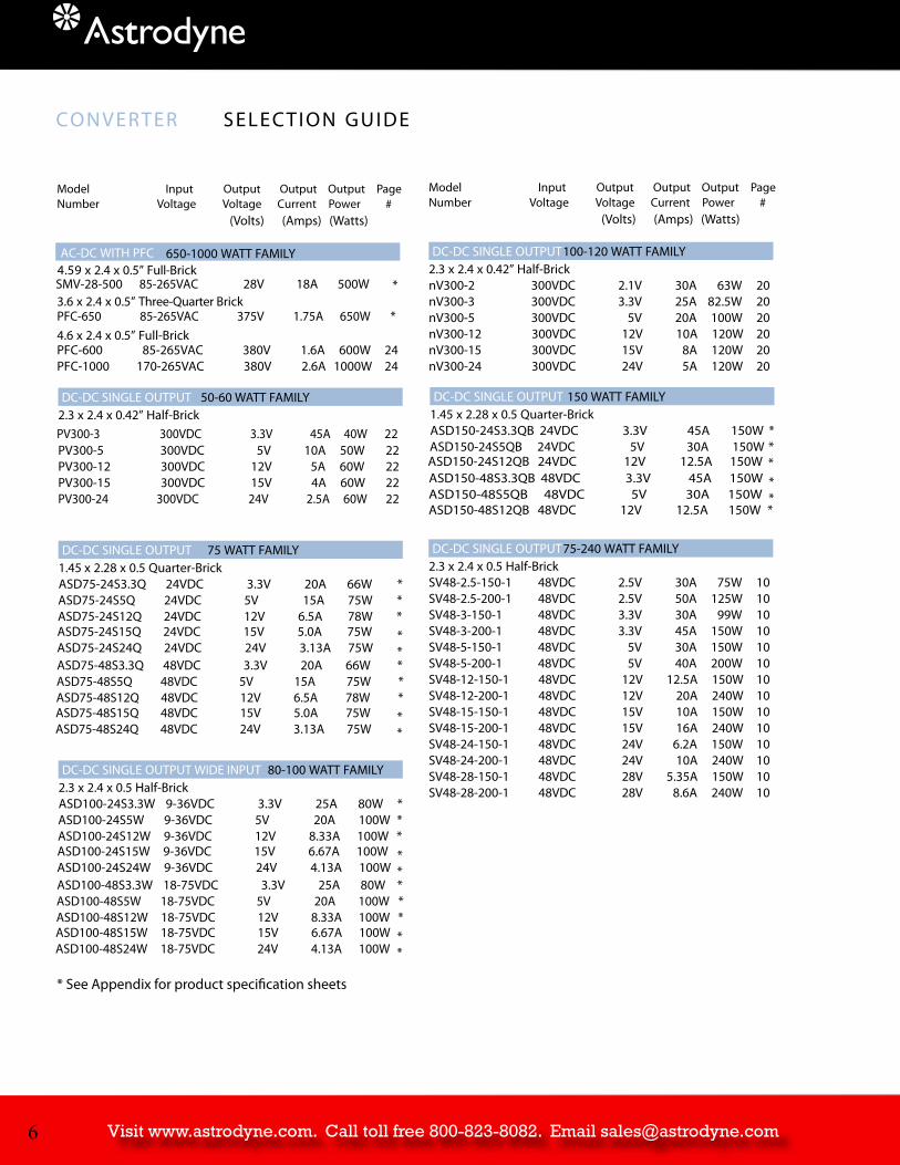
CONVERTER SELECTION GUIDE
Model Input Output Output Output PageNumber Voltage Voltage Current Power #
(Volts) (Amps) (Watts)
AC-DC WITH PFC
4.6 x 2.4 x 0.5” Full-Brick PFC-600 85-265VAC 380V 1.6A 600W 24PFC-1000 170-265VAC 380V 2.6A 1000W 24
Model Input Output Output Output PageNumber Voltage Voltage Current Power #
(Volts) (Amps) (Watts)
DC-DC SINGLE OUTPUT 100-120 WATT FAMILY 2.3 x 2.4 x 0.42” Half-BricknV300-2 300VDC 2.1V 30A 63W 20nV300-3 300VDC 3.3V 25A 82.5W 20nV300-5 300VDC 5V 20A 100W 20nV300-12 300VDC 12V 10A 120W 20nV300-15 300VDC 15V 8A 120W 20nV300-24 300VDC 24V 5A 120W 20
DC-DC SINGLE OUTPUT75-240 WATT FAMILY2.3 x 2.4 x 0.5 Half-BrickSV48-2.5-150-1 48VDC 2.5V 30A 75W 10SV48-2.5-200-1 48VDC 2.5V 50A 125W 10SV48-3-150-1 48VDC 3.3V 30A 99W 10SV48-3-200-1 48VDC 3.3V 45A 150W 10SV48-5-150-1 48VDC 5V 30A 150W 10SV48-5-200-1 48VDC 5V 40A 200W 10SV48-12-150-1 48VDC 12V 12.5A 150W 10SV48-12-200-1 48VDC 12V 20A 240W 10SV48-15-150-1 48VDC 15V 10A 150W 10SV48-15-200-1 48VDC 15V 16A 240W 10SV48-24-150-1 48VDC 24V 6.2A 150W 10SV48-24-200-1 48VDC 24V 10A 240W 10SV48-28-150-1 48VDC 28V 5.35A 150W 10SV48-28-200-1 48VDC 28V 8.6A 240W 10
DC-DC SINGLE OUTPUT WIDE INPUT 80-100 WATT FAMILY2.3 x 2.4 x 0.5 Half-BrickASD100-24S3.3W 9-36VDC 3.3V 25A 80W *
650-1000 WATT FAMILY
ASD100-24S5W 9-36VDC 5V 20A 100W *ASD100-24S12W 9-36VDC 12V 8.33A 100W *
*ASD100-24S15W 9-36VDC 15V 6.67A 100W
*ASD100-24S24W 9-36VDC 24V 4.13A 100WASD100-48S3.3W 18-75VDC 3.3V 25A 80W *ASD100-48S5W 18-75VDC 5V 20A 100W *ASD100-48S12W 18-75VDC 12V 8.33A 100W *
*ASD100-48S15W 18-75VDC 15V 6.67A 100W
*ASD100-48S24W 18-75VDC 24V 4.13A 100W
DC-DC SINGLE OUTPUT 150 WATT FAMILY1.45 x 2.28 x 0.5 Quarter-BrickASD150-24S3.3QB 24VDC 3.3V 45A 150W *ASD150-24S5QB 24VDC 5V 30A 150W *ASD150-24S12QB 24VDC 12V 12.5A 150W *
*ASD150-48S3.3QB 48VDC 3.3V 45A 150W
*ASD150-48S5QB 48VDC 5V 30A 150WASD150-48S12QB 48VDC 12V 12.5A 150W *
3.6 x 2.4 x 0.5” Three-Quarter Brick PFC-650 85-265VAC 375V 1.75A 650W *
DC-DC SINGLE OUTPUT 50-60 WATT FAMILY 2.3 x 2.4 x 0.42” Half-Brick
PV300-5 300VDC 5V 10A 50W 22PV300-12 300VDC 12V 5A 60W 22PV300-15 300VDC 15V 4A 60W 22PV300-24 300VDC 24V 2.5A 60W 22
* See Appendix for product specication sheets
PV300-3 300VDC 3.3V 45A 40W 22
DC-DC SINGLE OUTPUT 75 WATT FAMILY1.45 x 2.28 x 0.5 Quarter-BrickASD75-24S3.3Q 24VDC 3.3V 20A 66W *ASD75-24S5Q 24VDC 5V 15A 75W *ASD75-24S12Q 24VDC 12V 6.5A 78W *
*ASD75-24S15Q 24VDC 15V 5.0A 75W
*ASD75-24S24Q 24VDC 24V 3.13A 75WASD75-48S3.3Q 48VDC 3.3V 20A 66W *ASD75-48S5Q 48VDC 5V 15A 75W *ASD75-48S12Q 48VDC 12V 6.5A 78W *
*ASD75-48S15Q 48VDC 15V 5.0A 75W
*ASD75-48S24Q 48VDC 24V 3.13A 75W
SMV-28-500 85-265VAC 28V 18A 500W *4.59 x 2.4 x 0.5” Full-Brick
Model Input Output Output Output PageNumber Voltage Voltage Current Power #
(Volts) (Amps) (Watts)
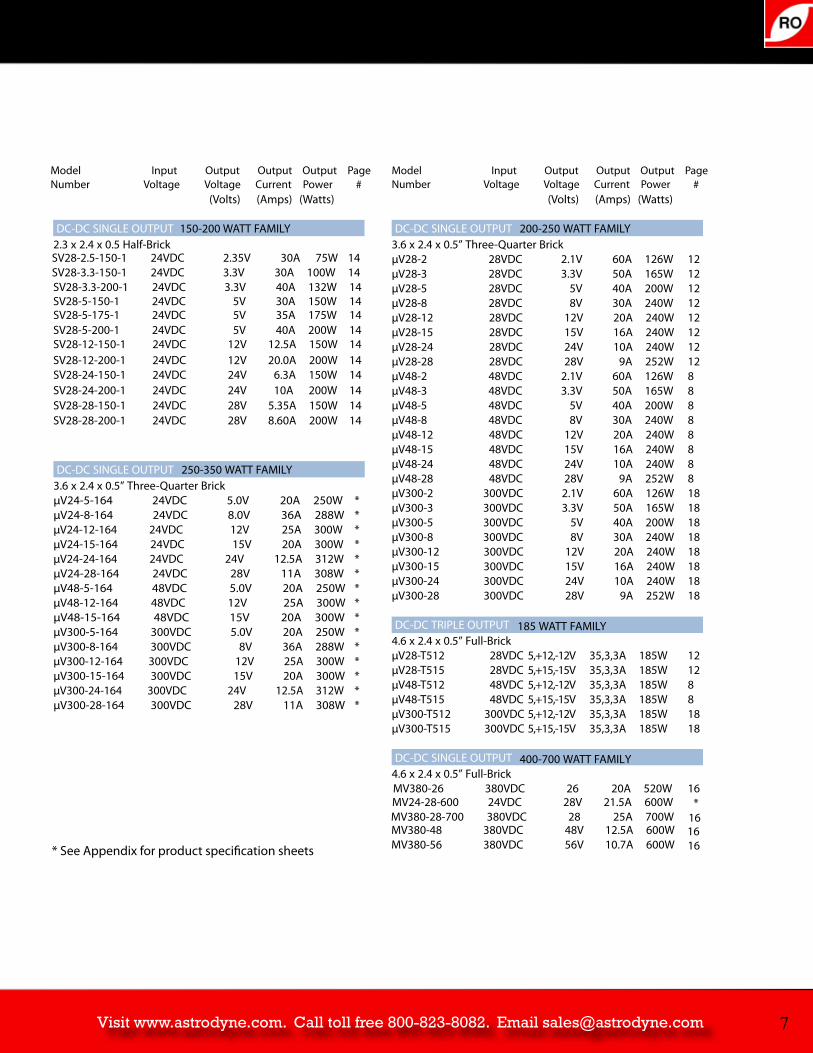
DC-DC SINGLE OUTPUT 150-200 WATT FAMILY 2.3 x 2.4 x 0.5 Half-Brick
SV28-3.3-150-1 24VDC 3.3V 30A 100W 14SV28-3.3-200-1 24VDC 3.3V 40A 132W 14
SV28-5-175-1 24VDC 5V 35A 175W 14
SV28-12-150-1 24VDC 12V 12.5A 150W 14
SV28-24-150-1 24VDC 24V 6.3A 150W 14
SV28-28-150-1 24VDC 28V 5.35A 150W 14
Model Input Output Output Output PageNumber Voltage Voltage Current Power #
(Volts) (Amps) (Watts)
DC-DC SINGLE OUTPUT 200-250 WATT FAMILY3.6 x 2.4 x 0.5” Three-Quarter BrickµV28-2 28VDC 2.1V 60A 126W 12µV28-3 28VDC 3.3V 50A 165W 12µV28-5 28VDC 5V 40A 200W 12µV28-8 28VDC 8V 30A 240W 12µV28-12 28VDC 12V 20A 240W 12µV28-15 28VDC 15V 16A 240W 12µV28-24 28VDC 24V 10A 240W 12µV28-28 28VDC 28V 9A 252W 12µV48-2 48VDC 2.1V 60A 126W 8µV48-3 48VDC 3.3V 50A 165W 8µV48-5 48VDC 5V 40A 200W 8µV48-8 48VDC 8V 30A 240W 8µV48-12 48VDC 12V 20A 240W 8µV48-15 48VDC 15V 16A 240W 8µV48-24 48VDC 24V 10A 240W 8µV48-28 48VDC 28V 9A 252W 8µV300-2 300VDC 2.1V 60A 126W 18µV300-3 300VDC 3.3V 50A 165W 18µV300-5 300VDC 5V 40A 200W 18µV300-8 300VDC 8V 30A 240W 18µV300-12 300VDC 12V 20A 240W 18µV300-15 300VDC 15V 16A 240W 18µV300-24 300VDC 24V 10A 240W 18µV300-28 300VDC 28V 9A 252W 18
DC-DC TRIPLE OUTPUT 185 WATT FAMILY4.6 x 2.4 x 0.5” Full-BrickµV28-T512 28VDC 5,+12,-12V 35,3,3A 185W 12µV28-T515 28VDC 5,+15,-15V 35,3,3A 185W 12µV48-T512 48VDC 5,+12,-12V 35,3,3A 185W 8µV48-T515 48VDC 5,+15,-15V 35,3,3A 185W 8µV300-T512 300VDC 5,+12,-12V 35,3,3A 185W 18µV300-T515 300VDC 5,+15,-15V 35,3,3A 185W 18
DC-DC SINGLE OUTPUT 400-700 WATT FAMILY4.6 x 2.4 x 0.5” Full-BrickMV380-26 380VDC 26 20A 520W 16
MV380-48 380VDC 48V 12.5A 600W 16MV380-56 380VDC 56V 10.7A 600W 16
SV28-2.5-150-1 24VDC 2.35V 30A 75W 14
SV28-5-150-1 24VDC 5V 30A 150W 14
SV28-5-200-1 24VDC 5V 40A 200W 14
SV28-12-200-1 24VDC 12V 20.0A 200W 14
SV28-24-200-1 24VDC 24V 10A 200W 14
SV28-28-200-1 24VDC 28V 8.60A 200W 14
DC-DC SINGLE OUTPUT 250-350 WATT FAMILY3.6 x 2.4 x 0.5” Three-Quarter BrickµV24-5-164 24VDC 5.0V 20A 250W *µV24-8-164 24VDC 8.0V 36A 288W *µV24-12-164 24VDC 12V 25A 300W *µV24-15-164 24VDC 15V 20A 300W *µV24-24-164 24VDC 24V 12.5A 312W *µV24-28-164 24VDC 28V 11A 308W *µV48-5-164 48VDC 5.0V 20A 250W *µV48-12-164 48VDC 12V 25A 300W *µV48-15-164 48VDC 15V 20A 300W *µV300-5-164 300VDC 5.0V 20A 250W *µV300-8-164 300VDC 8V 36A 288W *µV300-12-164 300VDC 12V 25A 300W *µV300-15-164 300VDC 15V 20A 300W *µV300-24-164 300VDC 24V 12.5A 312W *µV300-28-164 300VDC 28V 11A 308W *
* See Appendix for product specication sheets
MV380-28-700 380VDC 28 25A 700W 16MV24-28-600 24VDC 28V 21.5A 600W *
Visit www.astrodyne.com. Call toll free 800-823-8082. Email [email protected] 7
Model Input Output Output Output PageNumber Voltage Voltage Current Power #
(Volts) (Amps) (Watts)
DC-DC SINGLE OUTPUT 150-200 WATT FAMILY 2.3 x 2.4 x 0.5 Half-Brick
SV28-3.3-150-1 24VDC 3.3V 30A 100W 14SV28-3.3-200-1 24VDC 3.3V 40A 132W 14
SV28-5-175-1 24VDC 5V 35A 175W 14
SV28-12-150-1 24VDC 12V 12.5A 150W 14
SV28-24-150-1 24VDC 24V 6.3A 150W 14
SV28-28-150-1 24VDC 28V 5.35A 150W 14
Model Input Output Output Output PageNumber Voltage Voltage Current Power #
(Volts) (Amps) (Watts)
DC-DC SINGLE OUTPUT 200-250 WATT FAMILY3.6 x 2.4 x 0.5” Three-Quarter BrickµV28-2 28VDC 2.1V 60A 126W 12µV28-3 28VDC 3.3V 50A 165W 12µV28-5 28VDC 5V 40A 200W 12µV28-8 28VDC 8V 30A 240W 12µV28-12 28VDC 12V 20A 240W 12µV28-15 28VDC 15V 16A 240W 12µV28-24 28VDC 24V 10A 240W 12µV28-28 28VDC 28V 9A 252W 12µV48-2 48VDC 2.1V 60A 126W 8µV48-3 48VDC 3.3V 50A 165W 8µV48-5 48VDC 5V 40A 200W 8µV48-8 48VDC 8V 30A 240W 8µV48-12 48VDC 12V 20A 240W 8µV48-15 48VDC 15V 16A 240W 8µV48-24 48VDC 24V 10A 240W 8µV48-28 48VDC 28V 9A 252W 8µV300-2 300VDC 2.1V 60A 126W 18µV300-3 300VDC 3.3V 50A 165W 18µV300-5 300VDC 5V 40A 200W 18µV300-8 300VDC 8V 30A 240W 18µV300-12 300VDC 12V 20A 240W 18µV300-15 300VDC 15V 16A 240W 18µV300-24 300VDC 24V 10A 240W 18µV300-28 300VDC 28V 9A 252W 18
DC-DC TRIPLE OUTPUT 185 WATT FAMILY4.6 x 2.4 x 0.5” Full-BrickµV28-T512 28VDC 5,+12,-12V 35,3,3A 185W 12µV28-T515 28VDC 5,+15,-15V 35,3,3A 185W 12µV48-T512 48VDC 5,+12,-12V 35,3,3A 185W 8µV48-T515 48VDC 5,+15,-15V 35,3,3A 185W 8µV300-T512 300VDC 5,+12,-12V 35,3,3A 185W 18µV300-T515 300VDC 5,+15,-15V 35,3,3A 185W 18
DC-DC SINGLE OUTPUT 400-700 WATT FAMILY4.6 x 2.4 x 0.5” Full-BrickMV380-26 380VDC 26 20A 520W 16
MV380-48 380VDC 48V 12.5A 600W 16MV380-56 380VDC 56V 10.7A 600W 16
SV28-2.5-150-1 24VDC 2.35V 30A 75W 14
SV28-5-150-1 24VDC 5V 30A 150W 14
SV28-5-200-1 24VDC 5V 40A 200W 14
SV28-12-200-1 24VDC 12V 20.0A 200W 14
SV28-24-200-1 24VDC 24V 10A 200W 14
SV28-28-200-1 24VDC 28V 8.60A 200W 14
DC-DC SINGLE OUTPUT 250-350 WATT FAMILY3.6 x 2.4 x 0.5” Three-Quarter BrickµV24-5-164 24VDC 5.0V 20A 250W *µV24-8-164 24VDC 8.0V 36A 288W *µV24-12-164 24VDC 12V 25A 300W *µV24-15-164 24VDC 15V 20A 300W *µV24-24-164 24VDC 24V 12.5A 312W *µV24-28-164 24VDC 28V 11A 308W *µV48-5-164 48VDC 5.0V 20A 250W *µV48-12-164 48VDC 12V 25A 300W *µV48-15-164 48VDC 15V 20A 300W *µV300-5-164 300VDC 5.0V 20A 250W *µV300-8-164 300VDC 8V 36A 288W *µV300-12-164 300VDC 12V 25A 300W *µV300-15-164 300VDC 15V 20A 300W *µV300-24-164 300VDC 24V 12.5A 312W *µV300-28-164 300VDC 28V 11A 308W *
* See Appendix for product specication sheets
MV380-28-700 380VDC 28 25A 700W 16MV24-28-600 24VDC 28V 21.5A 600W *
Visit www.astrodyne.com. Call toll free 800-823-8082. Email [email protected]
UV48 MICROVERTER ® SERIES126-252 WATTS 48VDC INPUT 3/4 BRICK SINGLES FULL BRICK TRIPLES
DESCRIPTIONThe µV48 Series are high density DC-DC converters designed for use in telecom andother centralized modular and distributedpower applications. The µV48 Series use metalPC boards, planar transformers, and surfacemount construction to produce up to 252watts in a tiny package.
FEATURES• Miniature Size • High Density – Up to 58 W/in.3• Constant Frequency – 370KHZ• Parallelable with Current Sharing• Fault Tolerant – n+m Redundancy• Extremely Low Thermal Resistance• Output Good Signal• Optional Sync Pin• UL/CSA/TUV APPROVALS• Non-Shutdown OVP• Logic On-O• Thermal Protection• Current Limit/Short Circuit Protection
MODEL SELECTIONModel Output Output
Voltage CurrentµV48-2 2.1V 60AµV48-3 3.3V 50AµV48-5 5V 40AµV48-8 8V 30AµV48-12 12V 20AµV48-15 15V 16AµV48-24 24V 10AµV48-28 28V 9A
µV48-T512 5V 35A*12V 3A*
-12V 3A*
µV48-T515 5V 35A*15V 3A*
-15V 3A*
*Maximum Total Output Power 185 W.Option: – A Output Good Deleted
– S Sync. Pin Option
SINGLE OUTPUT
TRIPLE OUTPUT
168

Visit www.astrodyne.com. Call toll free 800-823-8082. Email [email protected]
UV48 MICROVERTER ® SERIES126-252 WATTS 48VDC INPUT 3/4 BRICK SINGLES FULL BRICK TRIPLES
DESCRIPTIONThe µV48 Series are high density DC-DC converters designed for use in telecom andother centralized modular and distributedpower applications. The µV48 Series use metalPC boards, planar transformers, and surfacemount construction to produce up to 252watts in a tiny package.
FEATURES• Miniature Size • High Density – Up to 58 W/in.3• Constant Frequency – 370KHZ• Parallelable with Current Sharing• Fault Tolerant – n+m Redundancy• Extremely Low Thermal Resistance• Output Good Signal• Optional Sync Pin• UL/CSA/TUV APPROVALS• Non-Shutdown OVP• Logic On-O• Thermal Protection• Current Limit/Short Circuit Protection
MODEL SELECTIONModel Output Output
Voltage CurrentµV48-2 2.1V 60AµV48-3 3.3V 50AµV48-5 5V 40AµV48-8 8V 30AµV48-12 12V 20AµV48-15 15V 16AµV48-24 24V 10AµV48-28 28V 9A
µV48-T512 5V 35A*12V 3A*
-12V 3A*
µV48-T515 5V 35A*15V 3A*
-15V 3A*
*Maximum Total Output Power 185 W.Option: – A Output Good Deleted
– S Sync. Pin Option
SINGLE OUTPUT
TRIPLE OUTPUT
16
UV48 MICROVERTER SERIES SPECIFICATIONS
Min Typical Max Units Conditions
INPUT CDV278463egatlov tupnItuptuo lluf %57CDV23 tuonworB
sbmoluoC4-01x6.2egrahc hsur nIInput re fl enil lanimon ,daol lluf%02elppir detce
selgnissttaw 5.2noitapissid rewop daol oN7.5 watts triples
sttaw1ni rewop delbasid cigoLzH 021 @Bd06 noitcejer elppir tupnI
stinu ot egamad onCDV00127 egatlovrevo tupnI
OUTPUT (Singles and Main Output of Triple)daol on%1±ycarucca tniop teS
daol lluf ot 0%2.20.noitaluger daoLegnar revo%2.20.noitaluger eniLzHM02 ot 0p-p%31elppiR
%01±egnar mirT consult factory for extended rangelatot V5.0noitasnepmoc esnes etomeR
OVP (non shutdown auto. recovery) 120* % * or Vout +.5V whichever is greaterdaol lluf%021-011)yrevocer.otua( timiL tnerruCdaol lluf%5±)citamotua( gnirahs tnerruC
sµ05selgnis esnopser tneisnarT 20-80% load,.5A/µs, Vout 1%sµ002 selpirt tuptuo niam esnopser tneisnarT 10-20A, aux. loads 2.5A,
.25A/µs, Vout 1%Transient response waveforms See web site: www.astrodyne.com
/%20.tfird pmeT °CEciency See Curves on Page 57
OUTPUT (Auxiliary Outputs of Triples)%1±5.0±ycarucca tniop teS 10A on main, no load auxiliaries
daol lluf ot 0%5.2. noitaluger daoLegnar revo%1.10. noitaluger eniL
zHm 02 ot 0p-p%5.52. elppiRdaol lluf %021-011)yrevocer.otua( timiL tnerruC
%1 nihtiw tuoV ,daol %08-02sµ002 esnopser tneisnarT%1 tuoV ,enil hgih ot enil wolsµ002 esnopser tneisnarT
%1 tuoV ,daol %001-05sµ002 esnopser tneisnarT/%60.tfird pmeT °C
CONTROL %1 tuoV ,deilppa rewop tupnism5.2 emit no-nruT%1 nihtiw tuoVsm1 emit no nrut cigoL
knisAm1 tnerruc delbasid cigoL
ISOLATION erudecorp rof yrotcaf tlusnocCDV0003tuptuo ot tupnICDV0051esac ot tupnICDV005esac ot tuptuO
Fp0022yticapac tuptuo ot tupnI
THERMAL Operating temperature -40 +100 °C caseAutomatic shut-down temperature +100 +105 +110 °C caseThermal resistance case to ambient 4.2 °C/w single @ Tc=100 °C
3.3 °C/w triple @ Tc=100 °C
WEIGHT .zo 7selgniS.zo 9selpirT
SIZE sehcni 6.3x4.2x5.0selgniSsehcni 6.4x4.2x5.0selpirT
RO Associates | Tel: 408.744.1450 | Fax: 408.744.1521 | email: [email protected]
17 9
Visit www.astrodyne.com. Call toll free 800-823-8082. Email [email protected]
0.400(10.16)
0.300(7.62)
0.300(7.62)
0.400(10.16)
0.30(7.6)
2.00(50.8)
2.40(61.0)
0.20(5.1)
0.224 Ø MAX(5.69 Ø MAX)MOUNTINGINSERTSM3x0.5 THRU4PL
2.28(57.9)
1.90(48.3)
0.19(4.8)
-IN
CASE
ON/OFF
+ IN
-OUT
-S
T
+ S
+ OUT
0.040 (1.02) Ø PINFUSED TINOVER COPPER7PL
0.080 (2.03) Ø PINFUSED TINOVER COPPER 2PL
ALUMINUM HEATSINK SURFACE
0.47(11.9)
0.40(10.2)
SEE OPTIONAL PIN LENGTHS 0.2 MIN
(5.1 MIN)
0.515 0.020(13.08 0.5)
18
SV48 SUPERVERTER ® 150/200 SERIES75-240 WATTS 48VDC INPUT 1/2 BRICK INDUSTRY STANDARD
MODEL SELECTIONModel Output Output
Voltage Current48 VDC(36-75V)SV48-2.5-150-1 2.5Vdc 30ASV48-2.5-200-1 2.5Vdc 50ASV48-3-150-1 3.3Vdc 30ASV48-3-200-1 3.3Vdc 45ASV48-5-150-1 5Vdc 30ASV48-5-200-1 5Vdc 40ASV48-12-150-1 12Vdc 12.5ASV48-12-200-1 12Vdc 20ASV48-15-150-1 15Vdc 10ASV48-15-200-1 15Vdc 16ASV48-24-150-1 24Vdc 6.2ASV48-24-200-1 24Vdc 10ASV48-28-150-1 28Vdc 5.35ASV48-28-200-1 28Vdc 8.6A
DESCRIPTIONThe SuperVerter 48 Series (150/200W) are high power density and high dynamic responseDC-DC converters designed for use in telecom,wireless, and other centralized modular or dis-tributed power systems. The SuperVerter familyof DC-DC converters may be used as form, fit,function replacements for the industry standardhalf bricks. If additional power is required theSV48-XX-200 family provides up to 50% morepower than industry standard modules.
FEATURES• Direct Replacement for Industry Standard • High E¥ciency• High MTBF (1.8 million hours) • Constant Frequency• Clamp Over Voltage Protection • Remote Sense • Trim Range: 60% to 110% • Encapsulated• High Power Density: up to 87 W/cu.in. • Low Noise • -40 ° to +100 ° C Baseplate Operation• Choice of On/O¨ Logic • Safety Agency Approved • Threaded or Thru Mounting Holes • Optional Pin lengths• Over Temperature Protection
OPTIONAL FEATURESFor the optional features listed below, simplylist the appropriate digit(s) for the features you want in ascending order in the su¥x following -150 or -200 in the part number .
Feature Options SuxNegative Logic On/O is standard include “1” in the suxPositive Logic On/O is optional delete “1” from the suxThreaded mounting holes, as shown in the outline drawing are standard no sux digit requiredOptional thru mounting holes (without threads) of 0.130” inside diameter* include “4” in the sux Pin length of 0.20” (5.1mm) is standard no sux digit requiredPin length of 0.145” (3.68mm)* include “6” in the suxPin length of 0.110” (2.79mm)* include “8” in the sux* Minimum order quantities apply.
Examples:SV48-5-200-1 Standard module negative logic, threaded inserts, 0.20inch pins.SV48-5-200-48 Positive logic, through hole inserts, 0.110 inch pins.SV48-5-200-146 Negative logic, through hole inserts, 0.145 inch pins.
10
Visit www.astrodyne.com. Call toll free 800-823-8082. Email [email protected]
RO Associates | Tel: 408.744.1450 | Fax: 408.744.1521 | email: [email protected]
19
SV48 SUPERVERTER (150/200) SERIES SPECIFICATIONS
Min Typical Max Units Conditions
Absolute Maximum Ratings: Exceeding absolute maximum ratings may cause permanent damage or reduce reliability.
PARAMETER suounitnoCcdV08egatloV tupnI.xam cesm 001cdV001egatloV tupnI tneisnarT
cdV0051noitalosI tuptuO/tupnIOperating Case Temperature -40 100 °CStorage Temperature -40 110 °C
Electrical Specifications: Apply over the entire range of input voltage, output current, and temperature unless indicated.
INPUT cdV578463egatloV tupnIA5.3051-5.2-84VS mumixaMA0.6002-5.2-84VStnerruC tupnIA5.4051-3-84VSA5.6002-3-84VSA5.6051-5-84VSA7.8002-5-84VSA5.6051-21-84VSA5.01002-21-84VSA5.6051-51-84VSA5.01002-51-84VSA5.6051-42-84VSA5.01002-42-84VSA6.5051-82-84VSA0.9002-82-84VS
zH 021@Bd06noitcejeR elppiR tupnI
OUTPUT 52 daoL lluF ,nI V84%2tnioP teS egatloV °CdaoL lluF ot 0%2.050.0noitalugeR daoL
egnaR niV revO%1.010.0noitalugeR eniLVoltage Drift w/TemperatureRipple See web site: www.astrodyne.comCurrent See Model Selection
,lanimon tuoV %09 = tuoV.xam tuoI %031511noitpecnI timiL tnerruCSee Output Characteristic Curves on web site
,Vm 052 = tuoVxam tuoI %071tnerruC tiucriC trohSSee Output Characteristic Curves on web site
Transient Response Peak Deviation 1 % Vout 50 to 75% or 50 to 25%egnahC daoL)etar wels cesµ/A1.0(
Transient Response Settling Time 100 µsec Vout within 1% Vout nominal(0.1A/µsec slew rate)Eciency See Curves on Page 56 or our web site: www.astrodyne.comExternal Load Capacitance 0 10,000 µF
ISOLATION Input to Output Capacitance 2000 pFsmho M01ecnatsiseR tuptuO ot tupnI
MECHANICAL ).zo( g)2.4( 811thgieWsehcni82.2x4.2x5.0eziS See Outline Drawing
Thermal Resistance Case to Ambient 6.6 °C/W Case Temperature = 100 °C
FEATURES tuoV%01106egnaR mirTV5.0noitasnepmoC esneS etomeR
Over Voltage Clamp See table on our website: www.astrodyne.comOver Temperature Shut-down 105 °C Case TemperatureLogic On/OLogic Low: Von/o¢0 1.2 V @ Ion/o¢ = 1 mA
V0 = ffo/noV @Am0.1ffo/noIAm 1 = ffo/noI @V51ffo/noV :hgiH cigoL
V51 = ffo/noV @Aµ05ffo/noI nihtiw tuoV ,daol %08cesm538emiT no-nruT
1% Vout nominal
See Input Characteristic Curvesfor each model on our web sitewww.roassoc.com
11

Visit www.astrodyne.com. Call toll free 800-823-8082. Email [email protected]
DESCRIPTIONThe µV28 Series are high density DC-DC converters designed for use in telecom and other centralized modular and distributedpower applications. The µV28 Series use metalPC boards, planar transformers, and surfacemount construction to produce up to 252watts in a tiny package.
FEATURES• Miniature Size • High Density – Up to 58 W/in.3• Constant Frequency – 370KHZ• Parallelable with Current Sharing• Fault Tolerant – n+m Redundancy• Extremely Low Thermal Resistance• Output Good Signal• Optional Sync Pin• Non-Shutdown OVP• Logic On-O• Thermal Protection• Current Limit/Short Circuit Protection
MODEL SELECTIONModel Output Output
Voltage CurrentµV28-2 2.1V 60AµV28-3 3.3V 50AµV28-5 5V 40AµV28-8 8V 30AµV28-12 12V 20AµV28-15 15V 16AµV28-24 24V 10AµV28-28 28V 9A
µV28-T512 5V 35A*12V 3A*
-12V 3A*
µV28-T515 5V 35A*15V 3A*
-15V 3A*
*Maximum Total Output Power 185 W.Option: – A Output Good Deleted
– S Sync. Pin Option
30
UV28 MICROVERTER ® SERIES126-252 WATTS 28VDC INPUT 3/4 BRICK SINGLES FULL BRICK TRIPLES
SINGLE OUTPUT
TRIPLE OUTPUT
12
Visit www.astrodyne.com. Call toll free 800-823-8082. Email [email protected]
DESCRIPTIONThe µV28 Series are high density DC-DC converters designed for use in telecom and other centralized modular and distributedpower applications. The µV28 Series use metalPC boards, planar transformers, and surfacemount construction to produce up to 252watts in a tiny package.
FEATURES• Miniature Size • High Density – Up to 58 W/in.3• Constant Frequency – 370KHZ• Parallelable with Current Sharing• Fault Tolerant – n+m Redundancy• Extremely Low Thermal Resistance• Output Good Signal• Optional Sync Pin• Non-Shutdown OVP• Logic On-O• Thermal Protection• Current Limit/Short Circuit Protection
MODEL SELECTIONModel Output Output
Voltage CurrentµV28-2 2.1V 60AµV28-3 3.3V 50AµV28-5 5V 40AµV28-8 8V 30AµV28-12 12V 20AµV28-15 15V 16AµV28-24 24V 10AµV28-28 28V 9A
µV28-T512 5V 35A*12V 3A*
-12V 3A*
µV28-T515 5V 35A*15V 3A*
-15V 3A*
*Maximum Total Output Power 185 W.Option: – A Output Good Deleted
– S Sync. Pin Option
30
UV28 MICROVERTER ® SERIES126-252 WATTS 28VDC INPUT 3/4 BRICK SINGLES FULL BRICK TRIPLES
SINGLE OUTPUT
TRIPLE OUTPUT
UV28 MICROVERTER SERIES SPECIFICATIONS
Min Typical Max Units Conditions
INPUT CDV238202egatlov tupnItuptuo lluf %57CDV81 tuonworB
sbmoluoC4-01x6.2egrahc hsur nIInput re fl enil lanimon ,daoL lluF%02elppir detce
selgnissttaw 5.1noitapissid rewop daol oN7.5 watts triples
sttaw53.ni rewop delbasid cigoLzH 021 @Bd06 noitcejer elppir tupnI
stinu ot egamad onCDV0623 egatlovrevo tupnI
OUTPUT (Singles and Main Output of Triple)daol on%1±ycarucca tniop teS
daoL lluF ot 0%2.20.noitaluger daoLegnar revo%2.20.noitaluger eniLzHM02 ot 0p-p%31elppiR
%01±egnar mirT consult factory for extended rangelatot V5.0noitasnepmoc esnes etomeR
OVP (non shutdown auto. recovery) 120* % * or Vout +.5V whichever is greaterdaoL lluF%021-011)yrevocer.otua( timiL tnerruCdaoLl lluF%5±)citamotua( gnirahs tnerruC
sµ05selgnis esnopser tneisnarT 20-80% load,.5A/µs, Vout 1%sµ002 selpirt tuptuo niam esnopser tneisnarT 10-20A, aux. loads 2.5A,
.25A/µs, Vout 1%Transient response See website: www.astrodyne.com
/%20.tfird pmeT °CEciency See Curves on Page 58
OUTPUT (Auxiliary Outputs of Triples)%1±5.0±ycarucca tniop teS 10A on main, no load auxiliaries
daol lluf ot 0%5.2. noitaluger daoLegnar revo%1.10. noitaluger eniL
zHm 02 ot 0p-p%5.52. elppiRdaoL lluF %021-011)yrevocer.otua( timiL tnerruC
%1 nihtiw tuoV ,daol %08-02sµ002 esnopser tneisnarT%1 tuoV ,enil hgih ot enil wolsµ002 esnopser tneisnarT
%1 tuoV ,daol %001-05sµ002 esnopser tneisnarT/%60.tfird pmeT °C
CONTROL sm5.2 emit no nruT input power applied, Vout 1%%1 nihtiw tuoVsm1 emit no nrut cigoL
knisAm1 tnerruc delbasid cigoL
ISOLATION erudecorp rof yrotcaf tlusnocCDV0001tuptuo ot tupnICDV0001esac ot tupnICDV002esac ot tuptuO
Fp0022yticapac tuptuo ot tupnI
THERMAL Operating temperature -40 +100 °C caseAutomatic shut down temperature +100 +105 +110 °C caseThermal resistance case to ambient 4.2 °C/w single @ Tc=100 °C
3.3 °C/w triple @ Tc=100 °C
WEIGHT .zo 7selgnis.zo 9selpirt
SIZE sehcni 6.3x4.2x5.0selgnissehcni 6.4x4.2x5.0selpirt
RO Associates | Tel: 408.744.1450 | Fax: 408.744.1521 | email: [email protected]
31 13

Visit www.astrodyne.com. Call toll free 800-823-8082. Email [email protected]
0.400(10.16)
0.300(7.62)
0.300(7.62)
0.400(10.16)
0.30(7.6)
2.00(50.8)
2.40(61.0)
0.20(5.1)
0.224 Ø MAX(5.69 Ø MAX)MOUNTINGINSERTSM3x0.5 THRU4PL
2.28(57.9)
1.90(48.3)
0.19(4.8)
-IN
CASE
ON/OFF
+ IN
-OUT
-S
T
+ S
+ OUT
0.040 (1.02) Ø PINFUSED TINOVER COPPER7PL
0.080 (2.03) Ø PINFUSED TINOVER COPPER 2PL
ALUMINUM HEATSINK SURFACE
0.47(11.9)
0.40(10.2)
SEE OPTIONAL PIN LENGTHS 0.2 MIN
(5.1 MIN)
0.515 0.020(13.08 0.5)
MODEL SELECTIONModel Output Output
Voltage Current28 VDC(18-36V)SV28-2.5-150-1 2.5V 30ASV28-3.3-150-1 3.3V 30ASV28-3.3-200-1 3.3V 40ASV28-5-150-1 5V 30ASV28-5-175-1 5V 35A
SV28-12-150-1 12V 12.5A
SV28-24-150-1 24V 6.3A
SV28-28-150-1 28V 5.35A
DESCRIPTIONThe SuperVerter 28 Series are high power density and high dynamic response DC-DC con-verters designed for use in telecom, wireless, andother centralized modular or distributed powersystems using 24V input. The SuperVerter 28family of DC-DC converters may be used as form, fit, function replacements for the industry standard half bricks.
FEATURES• Direct Replacement for Industry Standard • High Eciency• High MTBF (1.8 million hours) • Constant Frequency• Clamp Over Voltage Protection • Remote Sense • Trim Range: 60% to 110% • Encapsulated• High Power Density• Low Noise • -40 ° to +100 ° C Baseplate Operation• Choice of On/O¥ Logic • Safety Agency Approved • Threaded or Thru Mounting Holes • Optional Pin lengths• Over Temperature Protection
OPTIONAL FEATURESFor the optional features listed below, simplylist the appropriate digit(s) for the features you want in ascending order in the sux following -150 to -200 in the part number.
Feature Options SuxNegative Logic On/O is standard include “1” in the suxPositive Logic On/O is optional delete “1” from the suxThreaded mounting holes, as shown in the outline drawing are standard no sux digit requiredOptional thru mounting holes (without threads) of 0.130” inside diameter* include “4” in the sux Pin length of 0.20” (5.1mm) is standard no sux digit requiredPin length of 0.145” (3.68mm)* include “6” in the suxPin length of 0.110” (2.79mm)* include “8” in the sux* Minimum order quantities apply.
Examples:SV28-5-150-1 Standard module negative logic, threaded inserts, 0.20inch pins.SV28-5-150-48 Positive logic, through hole inserts, 0.110 inch pins.SV28-5-150-146 Negative logic, through hole inserts, 0.145 inch pins.
32
SV28 SUPERVERTER ® 150/175/200 SERIES75-240 WATTS 28VDC INPUT 1/2 BRICK INDUSTRY STANDARD
SV28-5-200-1 5V 40A
SV28-12-200-1 12V 20.0A
SV28-24-200-1 24V 10A
SV28-28-200-1 28V 8.60A
14

Visit www.astrodyne.com. Call toll free 800-823-8082. Email [email protected]
SV28 SUPERVERTER (150/175/200) SERIES SPECIFICATIONS
Min Typical Max Units Conditions
Absolute Maximum Ratings: Exceeding absolute maximum ratings may cause permanent damage or reduce reliability.
PARAMETER suounitnoCcdV04egatloV tupnI.xam cesm 001cdV05egatloV tupnI tneisnarT
cdV0051noitalosI tuptuO/tupnIOperating Case Temperature -40 100 °CStorage Temperature -40 110 °C
Electrical Specifications: Apply over the entire range of input voltage, output current, and temperature unless indicated.
INPUT cdV638281egatloV tupnIMaximum Input Current See web site: www.astrodyne.com
zH 021@Bd06noitcejeR elppiR tupnI
OUTPUT 52 daoL lluF ,nI V84%2tnioP teS egatloV °CdaoL lluF ot 0%2.050.0noitalugeR daoL
egnaR niV revO%1.010.0noitalugeR eniLVoltage Drift w/TemperatureRipple See web site: www.astrodyne.comCurrent See Model Selection
,lanimon tuoV %09 = tuoV.xam tuoI %031511noitpecnI timiL tnerruCSee Output Characteristic Curves
,Vm 052 = tuoVxam tuoI %071tnerruC tiucriC trohSSee Output Characteristic Curves
Transient Response Peak Deviation 3 % Vout 50 to 75% or 50 to 25%egnahC daoL)etar wels cesµ/A1.0(
Transient Response Settling Time 300 µsec Vout within 1% Vout nominal(0.1A/µsec slew rate)Eciency See Curves on Page 56 or web site: www.astrodyne.comExternal Load Capacitance 0 10,000 µF
ISOLATION Input to Output Capacitance 2000 pFsmho M01ecnatsiseR tuptuO ot tupnI
cdV0051tuptuO ot tupnIcdV0051esaC ot tupnIcdV005esaC ot tuptuO
MECHANICAL ).zo( g)2.4( 811thgieWsehcni82.2x4.2x5.0eziS See Outline Drawing
Thermal Resistance Case to Ambient 6.6 °C/W Case Temperature = 100 °C
FEATURES tuoV%01106egnaR mirTV5.0noitasnepmoC esneS etomeR
Over Voltage Clamp See web site: www.astrodyne.comOver Temperature Shut-down 105 °C Case Temperature
(Not in 50W and 75W models)Logic On/OLogic Low: Von/o¡0 1.2 V @ Ion/o¡ = 1 mA
V0 = ffo/noV @Am0.1ffo/noIAm 1 = ffo/noI @V51ffo/noV :hgiH cigoL
V51 = ffo/noV @Aµ05ffo/noI nihtiw tuoV ,daol %08cesm538emiT no-nruT
1% Vout nominal
RO Associates | Tel: 408.744.1450 | Fax: 408.744.1521 | email: [email protected]
33
15

Visit www.astrodyne.com. Call toll free 800-823-8082. Email [email protected]
MV380 MEGAVERTER ® SERIES500-600 WATTS 380VDC INPUT FULL BRICK HIGH POWER
DESCRIPTIONMegaVerter 380 DC-DC converters are high density, high power modules packaged in the industry standard full brick size (2.4 x 4.6 x 0.5 in) for circuit board mounting.They are primarily used in conjunction withPFC modules to create AC-DC high power, low pro file front ends.
FEATURES• High Eciency: 88-91%• Constant Frequency• -40 to +100 °C Operation• Remote Sense• Wide Trim Range• Encapsulated• Non-Shutdown Over Voltage Protection• High Power Density: 109 W/cu. in.• Low Noise• 105 °C Over Temperature Protection• Safety Agency Compliant• Parallelable with Current Sharing for
n+m Redundancy
MODEL SELECTIONInput Output Output
Voltage Current380 VDC(360-400V)MV380-26 26V 20.0AMV380-48 48V 12.5AMV380-56 56V 10.7A
MV380 MEGAVERTER SERIES SPECIFICATIONS
Min Typical Max Units Conditions
Absolute Maximum Ratings: Exceeding absolute maximum ratings may cause permanent damage or reduce reliability.
PARAMETER Input Voltage (+In to –In) -0.3 420 VdcEnable Voltage (Enable to –In) -0.3 6.0 VdcParallel Pin Voltage (ref to –In) -0.3 5.0 VdcStorage Temperature -55 +125 °COperating Temperature -40 +100 °C BaseplateSoldering Temperature (Wave Solder) 260 °C < 5 sec.Soldering Temperature (Hand Solder) 390 °C < 7 sec.
Electrical Specifications: Apply over the entire range of input voltage, output current, and temperature unless indicated.
INPUT cdV 004 083 063 egatloV tupnI A5.2 tnerruC tupnI mumixaM
zH021@ Bd 06 noitcejeR elppiR tupnI
.15
.56
.20
.204.204.60
4.30
ALUMINUM HEATSINKSURFACE
.098 DIA. PIN 2 PLACES
.040 DIA. PIN 9 PLACES
PARALLEL-IN
-OUT
NC +S-STRIM
+OUTNCNC.15
.27+IN
.28 DIA. X .19 DEEP4 PLACES.20
.20.25
.15
.143 DIA. THRU 4 PLACES
.50
2.00
.20 MIN.
2.40
.12
MV24-28-600 28V 21.5AMV380-28-700 28V 25A
16

Visit www.astrodyne.com. Call toll free 800-823-8082. Email [email protected]
MV380 MEGAVERTER ® SERIES500-600 WATTS 380VDC INPUT FULL BRICK HIGH POWER
DESCRIPTIONMegaVerter 380 DC-DC converters are high density, high power modules packaged in the industry standard full brick size (2.4 x 4.6 x 0.5 in) for circuit board mounting.They are primarily used in conjunction withPFC modules to create AC-DC high power, low pro file front ends.
FEATURES• High Eciency: 88-91%• Constant Frequency• -40 to +100 °C Operation• Remote Sense• Wide Trim Range• Encapsulated• Non-Shutdown Over Voltage Protection• High Power Density: 109 W/cu. in.• Low Noise• 105 °C Over Temperature Protection• Safety Agency Compliant• Parallelable with Current Sharing for
n+m Redundancy
MODEL SELECTIONInput Output Output
Voltage Current380 VDC(360-400V)MV380-26 26V 20.0AMV380-48 48V 12.5AMV380-56 56V 10.7A
MV380 MEGAVERTER SERIES SPECIFICATIONS
Min Typical Max Units Conditions
Absolute Maximum Ratings: Exceeding absolute maximum ratings may cause permanent damage or reduce reliability.
PARAMETER Input Voltage (+In to –In) -0.3 420 VdcEnable Voltage (Enable to –In) -0.3 6.0 VdcParallel Pin Voltage (ref to –In) -0.3 5.0 VdcStorage Temperature -55 +125 °COperating Temperature -40 +100 °C BaseplateSoldering Temperature (Wave Solder) 260 °C < 5 sec.Soldering Temperature (Hand Solder) 390 °C < 7 sec.
Electrical Specifications: Apply over the entire range of input voltage, output current, and temperature unless indicated.
INPUT cdV 004 083 063 egatloV tupnI A5.2 tnerruC tupnI mumixaM
zH021@ Bd 06 noitcejeR elppiR tupnI
.15
.56
.20
.204.204.60
4.30
ALUMINUM HEATSINKSURFACE
.098 DIA. PIN 2 PLACES
.040 DIA. PIN 9 PLACES
PARALLEL-IN
-OUT
NC +S-STRIM
+OUTNCNC.15
.27+IN
.28 DIA. X .19 DEEP4 PLACES.20
.20.25
.15
.143 DIA. THRU 4 PLACES
.50
2.00
.20 MIN.
2.40
.12
MV24-28-600 28V 21.5AMV380-28-700 28V 25A
RO Associates | Tel: 408.744.1450 | Fax: 408.744.1521 | email: [email protected]
35
MV380 MEGAVERTER SERIES SPECIFICATIONS
Min Typical Max Units Conditions
OUTPUT Voltage Set Point V083cdV 52.62 0.62 57.5262-083VM in, 25 °C, Full LoadV083cdV05.840.8405.7484-083VM in, 25 °C, Full LoadV083cdV05.650.6505.5565-083VM in, 25 °C, Full Load
daol lluF ot 0%6.03.0 noitalugeR daoLV revO%2.020.0 noitalugeR eniL in Range
/% 20.0 erutarepmeT/w tfirD egatloV °C -40 to +100 °CzHM02 ot zH5 p-p V%21 elppiR
Rated Current A0.02 062-083VM
A5.21084-083VMA7.01065-083VM
Output Power W 02562-083VMW00665-083VM dna 84-083VM
Current Limit Inception 115 120 130 % F.L. V out = 95% V out nominalV.L.F % 051 tnerruC tiucriC trohS out = 250 mV,
Transient Response Peak Deviation (1.0A/µsec slew rate) V %562-083VM out 25% to 75% Load ChangeV %565-083VM dna 84-083VM out 25% to 75% Load Change
Transient Response SettlingTime (1.0A/µsec slew rate) 100 µsec V out within 1% V out nominalEciency See Curves on Page 56
V % 8862-083VM in= 380V, Full Load, 70 °C Case,V%1965-083VM dna 84-083VM in= 380V, Full Load, 70 °C Case,
External Load Capacitance Fu003,3062-083VM
MV380-48 and MV380-56 0 1,000 uF
ISOLATION cdV0054noitalosI tuptuO/tupnIcdV005noitalosI tuptuO/esneScdV0052noitalosI etalP esaB/tupnIcdV005noitalosI etalP esaB/tuptuOcdV005noitalosI etalP esaB/esneS
Input to Output Capacitance 4300 pF Case Floatingsmho M 01 ecnatsiseR tuptuO ot tupnI
MECHANICAL ).zo(g)4.7(032 thgieW sehcnI 6.4 x 4.2 x 5.0 eziS See Outline Drawing
Thermal Resistance, Case to Ambient(Radiation plus natural convection) 3.3 °C/W Case Temperature = 100 °C
FEATURE ).L.F( daoL lluF %001 ot 01.L.F% 5± ycaruccA gnirahS rewoPTrim Range
cdV03**8162-083VM **200 mA minimum loadV02<cdV rof deriuqercdV150484-083VM
cdV068465-083VMcdV 5.0 noitasnepmoC esneS etomeR
Over Voltage Protection (Non-Shutdown, Auto. Recovery)52cdV630362-083VM ° C Case Temperature52cdV064584-083VM ° C Case Temperature52cdV27 6665-083VM ° C Case Temperature
Over Temperature Shut-down +100 +105 +110 °C Case TemperatureV ,.L.Fcesm006emiT nO-nruT out within 1% V out Nominal
Enable *V V 8.0 dlohserhT ffO cigoL out = 0
V @ Am 0.1 )ffO cigoL( tnerruC elbanE enable = 0VV 4.2 dlohserhT nO cigoL
V ,.L.F cesm 2 emiT nO-nruT cigoL out within 1% V out Nominal
*An open collector connection or equivalent is recommended for on/o control
17

Visit www.astrodyne.com. Call toll free 800-823-8082. Email [email protected]
DESCRIPTIONThe µV300 Series are high density DC-DC converters designed for use in telecom and other centralized modular and distributedpower applications. The µV300 Series usemetal PC boards, planar transformers, and surface mount construction to produce up to 252 watts in a tiny package.
FEATURES• Miniature Size • High Density – Up to 58 W/in.3• Constant Frequency – 370KHZ• Parallelable with Current Sharing• Fault Tolerant – n+m Redundancy• Extremely Low Thermal Resistance• Output Good Signal• Optional Sync Pin• Non-Shutdown OVP• Logic On-O• Thermal Protection• Current Limit/Short Circuit Protection• UL/CSA/TUV/CE MARK Approvals
MODEL SELECTIONModel Output Output
Voltage CurrentµV300-2 2.1V 60AµV300-3 3.3V 50AµV300-5 5V 40AµV300-8 8V 30AµV300-12 12V 20AµV300-15 15V 16AµV300-24 24V 10AµV300-28 28V 9A
µV300-T512 5V 35A*12V 3A*
-12V 3A*
µV300-T515 5V 35A*15V 3A*
-15V 3A*
*Maximum Total Output Power 185 W.Option: – A Output Good Deleted
– S Sync. Pin Option
SINGLE OUTPUT
TRIPLE OUTPUT
36
UV300 MICROVERTER ® SERIES126-252 WATTS 300VDC INPUT 3/4 BRICK SINGLES FULL BRICK TRIPLES
Note : Filled Pins (marked • ) are not provided in µV300 series models
18

Visit www.astrodyne.com. Call toll free 800-823-8082. Email [email protected]
UV300 MICROVERTER SERIES SPECIFICATIONS
Min Typical Max Units Conditions
INPUT CDV004003022egatlov tupnItuptuo lluf %57CDV081 tuonworB
sbmoluoC5-01x5.4egrahc hsur nIInput re fl enil lanimon ,daol lluf%02elppir detce
selgnissttaw 5.2noitapissid rewop daol oN7.5 watts triples
sttaw1ni rewop delbasid cigoL zH 021 @Bd06 noitcejer elppir tupnI
OUTPUT (Singles and Main Output of Triple)daol on%1±ycarucca tniop teS
daol lluf ot 0%2.20.noitaluger daoLegnar revo%2.20.noitaluger eniLzHM02 ot 0p-p%31elppiR
%01±egnar mirT consult factory for extended rangelatot V5.0noitasnepmoc esnes etomeR
OVP (non shutdown auto. recovery) 120* % * or Vout +.5V whichever is greaterdaol lluf%021-011)yrevocer.otua( timiL tnerruCdaol lluf%5±)citamotua( gnirahs tnerruC
sµ05selgnis esnopser tneisnarT 20-80% load,.5A/µs, Vout 1%sµ002 selpirt tuptuo niam esnopser tneisnarT 10-20A, aux. loads 2.5A,
.25A/µs, Vout 1%Transient response See web site: www.astrodyne.com
/%20.tfird pmeT °CEciency See Curves on Page 58
OUTPUT (Auxiliary Outputs of Triples)%1±5.0±ycarucca tniop teS 10A on main, no load auxiliaries
daol lluf ot 0%5.2. noitaluger daoLegnar revo%1.10. noitaluger eniL
zHm 02 ot 0p-p%5.52. elppiRdaol lluf %021-011)yrevocer.otua( timiL tnerruC
%1 nihtiw tuoV ,daol %08-02sµ002 esnopser tneisnarT%1 tuoV ,enil hgih ot enil wolsµ002 esnopser tneisnarT
%1 tuoV ,daol %001-05sµ002 esnopser tneisnarT/%60.tfird pmeT °C
CONTROL %1 tuoV ,deilppa rewop tupnism052 emit no nruT%1 nihtiw tuoVsm2 emit no nrut cigoL
knisAm1 tnerruc delbasid cigoL
ISOLATION erudecorp rof yrotcaf tlusnocCDV0054tuptuo ot tupnICDV0052esac ot tupnICDV005esac ot tuptuO
Fp0075yticapac tuptuo ot tupnI
THERMAL Operating temperature -40 +100 °C caseAutomatic shut down temperature +100 +105 +110 °C caseThermal resistance case to ambient 4.2 °C/w single @ Tc=100 °C
3.3 °C/w triple @ Tc=100 °C
WEIGHT .zo 7selgnis.zo 9selpirt
SIZE sehcni 6.3x4.2x5.0selgnissehcni 6.4x4.2x5.0selpirt
RO Associates | Tel: 408.744.1450 | Fax: 408.744.1521 | email: [email protected]
3719

Visit www.astrodyne.com. Call toll free 800-823-8082. Email [email protected]
DESCRIPTIONNanoVerter modules are high density DC-DC converters designed for use in telecom and other centralized modular and distributedpower applications. Two input voltage rangesare available and all use metal PC boards, planar transformers, and surface mount construction to produce up to 120 watts in a tiny package.
FEATURES• Miniature Size – Low Pro file .42 ”
–.32 ” with Recessed Mounting • Constant Frequency Operation• High Density – Up to 52 W/in. 3
• High Eciency• Extremely Low Thermal Resistance• 100 °C Baseplate Operation• Parallelable with Current Sharing• Fault Tolerant – True n+1... n+m • Redundancy• Hot Plug-In Capability• Secondary Referenced Controls• Auxiliary (housekeeping) Supply
Output (PV pin) • Logic On-O• Non-Shutdown Over Voltage Protection• Safety Agency Approved
MODEL SELECTIONInput Output Output
Voltage Current300 VDC (220-400V)nV300-2 2.1V 30AnV300-3 3.3V 25AnV300-5 5V 20AnV300-12 12V 10AnV300-15 15V 8AnV300-24 24V 5A
38
NV300 NANOVERTER ® SERIES63-120 WATTS 300VDC INPUT 1/2 BRICK SECONDARY REFERENCED
20
Visit www.astrodyne.com. Call toll free 800-823-8082. Email [email protected]
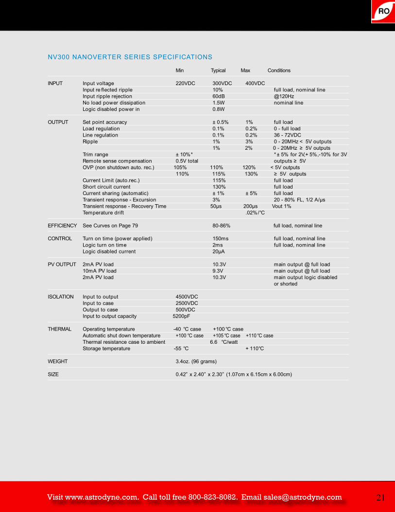
NV300 NANOVERTER SERIES SPECIFICATIONS
Min Typical Max Conditions
INPUT CDV004CDV003CDV022egatlov tupnIInput re fl enil lanimon ,daol lluf%01 elppir detce
zH021@Bd06noitcejer elppir tupnIenil lanimonW5.1noitapissid rewop daol oN
W8.0ni rewop delbasid cigoL
OUTPUT daol lluf%1%5.0±ycarucca tniop teSdaol lluf - 0%2.0%1.0noitaluger daoLCDV27 - 63%2.0%1.0 noitaluger eniL
stuptuo V5 < zHM02 - 0%3%1 elppiR1% 2% 0 - 20MHz ≥ 5V outputs
V3 rof %01-,%5+,V2 rof %5±**%01±egnar mirT stuptuolatot V5.0noitasnepmoc esnes etomeR ≥ 5V
OVP (non shutdown auto. rec.) 105% 110% 120% < 5V outputs110% 115% 130% ≥ 5V outputs
daol lluf%511).cer.otua( timiL tnerruCdaol lluf%031tnerruc tiucric trohSdaol lluf%5±%1±)citamotua( gnirahs tnerruC
sµ/A 2/1 ,LF %08 - 02%3noisrucxE - esnopser tneisnarTTransient response - Recovery Time 50µs 200µs Vout 1%
/%20.tfird erutarepmeT °C
EFFICIENCY See Curves on Page 79 80-86% full load, nominal line
CONTROL enil lanimon ,daol llufsm051 )deilppa rewop( emit no nruTenil lanimon ,daol llufsm2 emit no nrut cigoL
Aµ02tnerruc delbasid cigoL
PV OUTPUT daol lluf @ tuptuo niamV3.01 daol VP Am2daol lluf @ tuptuo niamV3.9 daol VP Am01
delbasid cigol tuptuo niamV3.01daol VP Am2or shorted
ISOLATION CDV0054tuptuo ot tupnICDV0052esac ot tupnI
CDV005esac ot tuptuOInput to output capacity 5200pF
THERMAL Operating temperature -40 °C case +100 °C caseAutomatic shut down temperature +100 °C case +105 °C case +110 °C caseThermal resistance case to ambient 6.6 °C/wattStorage temperature -55 ° 011+C °C
WEIGHT 3.4oz. (96 grams)
SIZE 0.42” x 2.40” x 2.30” (1.07cm x 6.15cm x 6.00cm)
RO Associates | Tel: 408.744.1450 | Fax: 408.744.1521 | email: [email protected]
3921

Visit www.astrodyne.com. Call toll free 800-823-8082. Email [email protected]
0.116 ØTHRU4 PL
0.108 Ø PIN2 PL
0.22 Ø X 0.10 DEEP4 PL
ALUMINUM HEATSINK SURFACE
2.40
.42
0.040 Ø PIN6 PL
2.30
1.96
.33
.40
.30
.30
.40
.17
1.90
2.06
.17
.03
-OUT
-S
T+S
+OUT
-IN
ON/OFF
+IN
DESCRIPTIONPicoVerter modules are high density DC-DC converters designed for use in telecom and other centralized modular and distributedpower applications. All use metal PC boards, planar transformers, and surface mount construction to produce up to 60 watts in a tiny package.
FEATURES• Miniature Size – Low Pro file .42 ” • High Eciency• Low Cost• Industry Standard Pin-out• Low Thermal Resistance• 100 °C Baseplate Operation• Constant Frequency Operation• Non-Shutdown Over Voltage Protection• Logic On/O• Fully Automated Manufacturing• UL/CSA/TUV/CE MARK
MODEL SELECTIONInput Output Output
Voltage Current300 VDC (220-400V)pV300-3 3.3V 12.5ApV300-5 5V 10ApV300-12 12V 5ApV300-15 15V 4ApV300-24 24V 2.5A
40
PV300 PICOVERTER ® SERIES40-60 WATTS 300VDC INPUT 1/2 BRICK LOW COST
22

Visit www.astrodyne.com. Call toll free 800-823-8082. Email [email protected]
PV300 PICOVERTER SERIES SPECIFICATIONS
Min Typical Max Conditions
INPUT Input voltage 220VDC 300VDC 400VDCInput reflected ripple 10% full load, nominal line
OUTPUT Set point accuracy ±0.5% ±1% full loadLoad regulation 0.1% 0.2% 0 - full loadLine regulation 0.1% 0.2% 220 - 400VDCRipple 1% 3% 0 - 20MHz Trim range ±10%Remote sense compensation 0.5V totalOVP (non shutdown auto. recovery) 110% 115% 130%Current Limit (auto.recovery) 115%Short circuit current 130%Transient response -
Excursion 2% (20-80% full load, 0.5 A/us)Recovery Time 50µs 200µs Vout 1%
Temperature drift .02%/°C
ISOLATION Input to output 4500VDCInput to case 2500VDCOutput to case 500VDC
THERMAL Operating temperature -40°C case +100°C caseAutomatic shut down temperature +100°C case +105°C case +110°C caseThermal resistance case to ambient 6.6 °C/wStorage temperature -55°C +110°C
WEIGHT 3.4oz. (96 grams)
SIZE 0.42” x 2.40” x 2.30” (1.07cm x 6.10cm x 5.84cm)
RO Associates | Tel: 408.744.1450 | Fax: 408.744.1521 | email: [email protected]
41 23

Visit www.astrodyne.com. Call toll free 800-823-8082. Email [email protected]
PFC UNIVERTER ® SERIES375-1000 WATTS 85-265VAC INPUT 3 / 4 ” & FULL BRICK POWER FACTOR
MODEL SELECTIONModel Input Output OutputNumber Voltage Voltage Power*
PFC-650 85-265VAC 375VDC 650 WattsPFC-1000 170-265VAC 380VDC 1000 Watts* See Derating Specification
DESCRIPTIONUniVerter PFC modules accept 85-265 VAC(PFC-600, PFC-650) or 170-265 VAC (PFC-1000) and convert it to 380 VDC to power 300VDC inputDC-DC converters. Power factor correctionmeets low harmonic distortion requirements of IEC 1000-3-2 and the European EN55022emissions speci fication when used with theModel HH-1199-6 EMI filter. UniVerter modulesutilize a boost converter incorporating a solidstate series switch for active inrush and shortcircuit current limiting. The series switch is also used to provide over temperature shutdown with automatic recovery.
FEATURES• 600, 650 & 1000 Watts• UL/CSA/TUV/CE MARK• Meets European EN55022 Emissions
when used with HH-1199-6 EMI Filter• Unity Power Factor• High Eciency• Active Inrush Limiting and Short Circuit
Protection• Very Low Harmonic Distortion• Auxiliary Supply• Power Fail Warning Via DC OK Signal• Load Enable Signal to Control DC-DC
Converters• Very Low Thermal Resistance• Superior Thermal Design• 100 °C Baseplate Operation
PFC-600 85-265VAC 380VDC 600 Watts
24

Visit www.astrodyne.com. Call toll free 800-823-8082. Email [email protected]
PFC UNIVERTER ® SERIES375-1000 WATTS 85-265VAC INPUT 3 / 4 ” & FULL BRICK POWER FACTOR
MODEL SELECTIONModel Input Output OutputNumber Voltage Voltage Power*
PFC-650 85-265VAC 375VDC 650 WattsPFC-1000 170-265VAC 380VDC 1000 Watts* See Derating Specification
DESCRIPTIONUniVerter PFC modules accept 85-265 VAC(PFC-600, PFC-650) or 170-265 VAC (PFC-1000) and convert it to 380 VDC to power 300VDC inputDC-DC converters. Power factor correctionmeets low harmonic distortion requirements of IEC 1000-3-2 and the European EN55022emissions speci fication when used with theModel HH-1199-6 EMI filter. UniVerter modulesutilize a boost converter incorporating a solidstate series switch for active inrush and shortcircuit current limiting. The series switch is also used to provide over temperature shutdown with automatic recovery.
FEATURES• 600, 650 & 1000 Watts• UL/CSA/TUV/CE MARK• Meets European EN55022 Emissions
when used with HH-1199-6 EMI Filter• Unity Power Factor• High Eciency• Active Inrush Limiting and Short Circuit
Protection• Very Low Harmonic Distortion• Auxiliary Supply• Power Fail Warning Via DC OK Signal• Load Enable Signal to Control DC-DC
Converters• Very Low Thermal Resistance• Superior Thermal Design• 100 °C Baseplate Operation
PFC-600 85-265VAC 380VDC 600 Watts
PFC UNIVERTER SERIES SPECIFICATIONS
PFC-600 PFC-1000
Power (Watts) 600 W 1000 WDerate output power linearly below Derate output power linearly below105 VAC from 600W at 105 VAC 205 VAC from 1000W at 205 VACto 400W at 85 VAC to 750W at 170 VAC
Input Range 85-265 VAC 170-265 VACInput Frequency 47-63 Hz (operation up to 440Hz is 47-63 Hz (operation up to 440Hz is
available with reduced specifications) available with reduced specifications)Power Factor .99 .99Harmonic Distortion <5% (conforming to IEC 1000-3-2) <5% (conforming to IEC 1000-3-2)Output Voltage 380 VDC 380 VDCEfficiency See Curves on Page 79 90/94 % (120/240 VAC) typical 94 % (240 VAC input)Inrush Limiting <15 A peak typical 30 A (max)Short Circuit Protection Trip point 1.8 A (Shutdown, automatic 2.8 A (Shutdown, automatic
recovery after removal of short) recovery after removal of short) Thermal Protection 105-110°C 105-110°C
(Shutdown, automatic recovery) (Shutdown, automatic recovery)Auxiliary Supply 14 V @ 10 mA 14 V, @10 mADC OK Signal Provides power fail warning when Provides power fail warning when
output drops below 355VDC output drops below 355VDCLoad Enable Direct interface with MicroVerter, Direct interface with MicroVerter
MegaVerter and PicoVerter DC-DC MegaVerter and PicoVerter DC-DC Converter logic on/off pin Converter logic on/off pin
Operating Temp. -40 to +100°C Case -40 to +100°C CaseOvervoltage Protection 415 VDC non-shutdown 415 VDC non-shutdownSafety UL1950, CSA22.2-234-M90, UL1950, CSA22.2-234-M90,
EN 60950 EN 60950Thermal Resistance (Case To Ambient) 3.3°C/W 3.3°C/W Isolation: Input-Output Non-isolated Non-isolated
Input/Output-Case 2500 VDC 2500 VDC
SYSTEM DIAGRAM
RO Associates | Tel: 408.744.1450 | Fax: 408.744.1521 | email: [email protected]
43
AC INPUT EMIFILTER
UNIVERTERPOWERFACTOR
CORRECTIONMODULE
HOLD UPCAP
300V INPUT DC-DCCONVERTER MODULE
300V INPUT DC-DCCONVERTER MODULE
300V INPUT DC-DCCONVERTER MODULE
25

Visit www.astrodyne.com. Call toll free 800-823-8082. Email [email protected]
MOUNTING BOARDS
DESCRIPTIONRO Mounting Boards provide an off- the-shelfsolution to convert PC mount pins to chassismount terminal strips. The ready to use PCboards contain many user features. The MountingBoards are perfect for prototypes and otherlow volume applications.
FEATURES• Conversion From Pins To Wire Terminals• Instant PC Design• Large Stud Terminals For High Current Output• Ground Plane To Shield Noise• Remote Sense Jumpers (DC-DC Models)• Fuse Protection• Plated Through Holes• 4 Through Holes For Customized Mounting• 4 Standoffs To Mate With Converters• Solder or Socket Mount
BOARD SELECTIONMounting Board ModuleSingle Output MicroVerter:MB-S* uV28 or uV48 SingleMB300-S* uV300 Single
Triple Output MicroVerter:MB-T* uV28 or uV48 TripleMB300-T* uV300 Triple
NanoVerter and PicoVerter:nV-MB* nV48nV300-MB* nV300pV-MB* pV48pV300-MB* pV300
Single Output SuperVerter:SV-MB* sV28 or sV48 Single
PFC-600 & PFC-1000:MB-PFC-SKT PFC-600 or PFC-1000*Add suffix - SKT for optional sockets.
TABLE 1: Dimension “A” ValuesModel Diameter “A”MB-S 0.10MB-S-SKT 0.26MB300-S 0.10MB300-S-SKT 0.26
TABLE 2: Terminal AssignmentsTerminal MB-S MB300-S 1 +V In +V In2 Parallel On/Off N/C3 -V In Parallel On/Off4 Optional Sync -V In5 Case Optional Sync6 Not Provided N/C7 Not Provided Case8 Output Good Output Good9 -Sense -Sense10 Trim Trim11 +Sense +Sense12 +V Out +V Out13 -V Out -V Out
Note: -SKT models have the same pin-outs as corresponding non-SKT models.
SINGLE OUTPUT MICROVERTER BOARDS
PFC-600 AND PFC-1000 BOARDS
(SEE TABLE 1)
26

Visit www.astrodyne.com. Call toll free 800-823-8082. Email [email protected]
RO Associates | Tel: 408.744.1450 | Fax: 408.744.1521 | email: [email protected]
47
TABLE 2: Dimension “A” ValuesModel Dia. “A” SV-MB 0.16SV-MB-SKT 0.32
TABLE 3: Terminal AssignmentsTerminal SV-MB1 +V In2 On/Off3 -V In4 Case5 -S6 T7 +S8 -V Out9 +V Out
Note: -SKT models have the same pin-outs as corresponding non-SKT models.
TABLE 5: Dimension “A” ValuesModel Diameter “A”MB-T 0.10MB-T-SKT 0.32MB300-T 0.10MB300-T-SKT 0.32
TABLE 6: Terminal AssignmentsTerminal MB-T MB300-T 1 +V In +V In2 Parallel On/Off N/C3 -V In Parallel On/Off4 Optional Sync -V In5 Case Optional Sync6 Not Provided N/C7 Not Provided Case8 Output Good Output Good9 -Sense -Sense10 Trim Trim11 +Sense +Sense12 +Output V1 +Output V113 -Output V1 -Output V114 -Output V2 -Output V215 +Output V2 +Output V216 -Output V3 -Output V317 +Output V3 +Output V3
Note: -SKT models have the same pin-outs as corresponding non-SKT models.
TABLE 7: Dimension “A” ValuesModel Diameter “A”NV-MB 0.15NV-MB-SKT 0.22NV300-MB 0.15NV300-MB-SKT 0.22PV-MB 0.15PV-MB-SKT 0.32PV300-MB 0.15PV300-MB-SKT 0.32
TABLE 8: Terminal AssignmentsTerminal NV-MB NV300-MB PV-MB/PV300-MB 1 Not Provided Case +V In2 Case N/C On/Off3 -V In -V In -V In4 +V In +V In Case5 +V Out +V Out -Out6 +V Out +V Out -Out7 -V Out -V Out -Sense8 -V Out -V Out Trim9 On/Off On/Off +Sense10 Trim Trim +Out11 +Sense +Sense +Out12 -Sense -Sense Not Provided13 Parallel Share Not Provided14 PV Not Provided Not Provided
Note: -SKT models have the same pin-outs as corresponding non-SKT models.
SINGLE OUTPUT SUPERVERTER BOARDS
NANOVERTER AND PICOVERTER BOARDS
(SEE TABLE 5)
(SEE TABLE 7)
(SEE TABLE 3)
TRIPLE OUTPUT MICROVERTER BOARDS
27

Visit www.astrodyne.com. Call toll free 800-823-8082. Email [email protected]
EVALUATION BOARDS
• FAST & ACCURATE EVALUATION
• SINGLE & MULTIPLE MODULE BOARDS
• PARALLELING DEMONSTRATION
• AC & DC INPUT BOARDS
DESCRIPTIONA wide range of Single and Multiple ModuleEvaluation Boards are available whether youare interested in demonstrating a power systemwith paralleled modules, n+m redundancy, and PFC or just evaluating a single module.
FEATURES• Paralleling • Redundancy & Hot Plug-In • Single High Power Output • Power Factor Correction, Current
Limiting, Thermal Protection, Logic On-Off, Output Good, ...
• Current Sharing• Universal AC In/Low VDC Out• Output Voltage Trimming
Evaluation Boards are excellent for poweringprototype circuits affording fast and accurateengineering design, testing, and evaluation.
Also, AC input boards are available for our300V series of MicroVerter Modules.
28

Visit www.astrodyne.com. Call toll free 800-823-8082. Email [email protected]
EVALUATION BOARDS
• FAST & ACCURATE EVALUATION
• SINGLE & MULTIPLE MODULE BOARDS
• PARALLELING DEMONSTRATION
• AC & DC INPUT BOARDS
DESCRIPTIONA wide range of Single and Multiple ModuleEvaluation Boards are available whether youare interested in demonstrating a power systemwith paralleled modules, n+m redundancy, and PFC or just evaluating a single module.
FEATURES• Paralleling • Redundancy & Hot Plug-In • Single High Power Output • Power Factor Correction, Current
Limiting, Thermal Protection, Logic On-Off, Output Good, ...
• Current Sharing• Universal AC In/Low VDC Out• Output Voltage Trimming
Evaluation Boards are excellent for poweringprototype circuits affording fast and accurateengineering design, testing, and evaluation.
Also, AC input boards are available for our300V series of MicroVerter Modules.
RO Associates | Tel: 408.744.1450 | Fax: 408.744.1521 | email: [email protected]
49
SINGLE MODULE EVALUATION BOARDS
SINGLE MODULE BOARDSEvaluation Board ModuleDC Input Boards:pV-EB 48 Series PicoVerterpV300-EB 300 Series PicoVerter
nV-EB 48 Series NanoVerternV300-EB 300 Series NanoVerter
EB28-S-1 28 Series Single Output MicroVerterEB48-S-1 48 Series Single Output MicroVerterEB28-T 28 Series Triple Output MicroVerterEB48-T 48 Series Triple Output MicroVerterEB-MV48 48 Series Single Output MegaVerterEB-SV 48/28 Series Single Output SuperVerterEB-SVD 48 Series Dual Output SuperVerterEB-SYV 48 Series Single Output SyncroVerterEB-SYVHC 48 Series Single Output SyncroVerter HC
AC Input Boards:EB300-S-1 300 Series Single Output MicroVerterEB300-T 300 Series Triple Output MicroVerterEB-PFC PFC-600/1000EB-PFC-MV380-26 PFC-600 and MV380-26EB-PFC-MV380-48 PFC-600 and MV380-48EB-PFC-MV380-56 PFC-600 and MV380-56
AC INPUT BOARDS
FEATURES• Sockets for Convenient Installation• Transistor for Electronic Logic On/Off• Solid State Relay for Convenient On/Off Switch• Dip Switch for Multiple Trim Networks• Pot & Trim Network to Check Adjustment Range• LED to Check Output Good Signal• Barrier Strips for Convenient Hook-Up • Large Stud Terminals for High Current Outputs• Zener Spike Protection for Parallel Pin• Ground Plane to Reduce Noise• Sync Terminal to Check Synchronization Option• Remote Sense Jumpers• Frame Holes for Easy Fan Mounting• Complete AC-DC Power Supply*• Built-In EMI Filter*• Convenient IEC 320 Receptable*• 110/220 VAC Selector Switch*
* AC Input Boards only
DC INPUT BOARDS
MEGAVERTER
MICROVERTER
PFC-MEGAVERTERSERIES
29
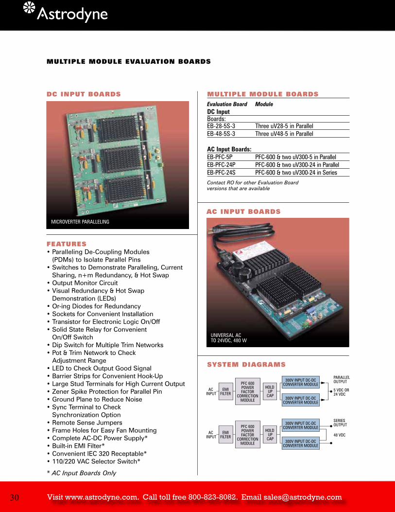
Visit www.astrodyne.com. Call toll free 800-823-8082. Email [email protected]
FEATURES• Paralleling De-Coupling Modules
(PDMs) to Isolate Parallel Pins• Switches to Demonstrate Paralleling, Current
Sharing, n+m Redundancy, & Hot Swap• Output Monitor Circuit• Visual Redundancy & Hot Swap
Demonstration (LEDs)• Or-ing Diodes for Redundancy• Sockets for Convenient Installation• Transistor for Electronic Logic On/Off• Solid State Relay for Convenient
On/Off Switch• Dip Switch for Multiple Trim Networks• Pot & Trim Network to Check
Adjustment Range• LED to Check Output Good Signal• Barrier Strips for Convenient Hook-Up• Large Stud Terminals for High Current Output• Zener Spike Protection for Parallel Pin• Ground Plane to Reduce Noise• Sync Terminal to Check
Synchronization Option• Remote Sense Jumpers• Frame Holes for Easy Fan Mounting• Complete AC-DC Power Supply*• Built-in EMI Filter*• Convenient IEC 320 Receptable*• 110/220 VAC Selector Switch*
* AC Input Boards Only
MULTIPLE MODULE BOARDSEvaluation Board ModuleDC Input Boards:EB-28-5S-3 Three uV28-5 in ParallelEB-48-5S-3 Three uV48-5 in Parallel
AC Input Boards:EB-PFC-5P PFC-600 & two uV300-5 in ParallelEB-PFC-24P PFC-600 & two uV300-24 in ParallelEB-PFC-24S PFC-600 & two uV300-24 in Series
Contact RO for other Evaluation Board versions that are available
MULTIPLE MODULE EVALUATION BOARDS
DC INPUT BOARDS
AC INPUT BOARDS
SYSTEM DIAGRAMS
MICROVERTER PARALLELING
UNIVERSAL ACTO 24VDC, 480 W
AC INPUT
EMIFILTER
PFC 600POWERFACTOR
CORRECTIONMODULE
PARALLELOUTPUT
5 VDC OR24 VDC
HOLD UP
CAP
300V INPUT DC-DCCONVERTER MODULE
300V INPUT DC-DCCONVERTER MODULE
AC INPUT
EMIFILTER
PFC 600POWERFACTOR
CORRECTIONMODULE
SERIESOUTPUT
48 VDCHOLD
UPCAP
300V INPUT DC-DCCONVERTER MODULE
300V INPUT DC-DCCONVERTER MODULE
30

Visit www.astrodyne.com. Call toll free 800-823-8082. Email [email protected]
LOADLINE
C1
L1
L2 L3 C4
C1–1.0µFL1,2=190µH
C2,7=.33µFL3,4=2x5.7mH
C3–6=.01µFR1=235kΩ
R1
C3 C5
C7
C6
C2
L4
DESCRIPTIONThe HH-1199-6 fi lter has been designed especially for the UniVerter Series of AC-DCconverters with Power Factor Correction. This fi lter works well to meet the newEuropean EN55022 emissions speci fication or for systems required to meet the FCC conducted emissions standards.
SPECIFICATIONSOperating Voltage 125/250 VACOperating Current (max) 6.0 A
zH 06 / 05ycneuqerFTemperature Range (storage) -40 to 85 °CTemperature Range (operating) -20 to 50 °CDiel. Withstanding Voltage (ph-case) 1500 VACDiel. Withstanding Voltage (ph-ph) 1500 VDCLeakage Current at 250 VAC, 60 Hz 2.5 mA maxDischarge Voltage After 60 Seconds 34 V max
OUTLINE DIAGRAM
RO Associates | Tel: 408.744.1450 | Fax: 408.744.1521 | email: [email protected]
51
EMI FILTERMODEL HH-1199-6 250 VAC 6A
CIRCUIT DIAGRAM
INSERTION LOSS
FREQUENCY (MHz)
INS
ER
TIO
N L
OS
S (d
B)
100
90
80
70
60
50
40
30
20
10
0.01 .02 .04 .1 .2 .4 1 2 4 10 20 40 100
CM
DM
4.204.60
1.00
.080 DIA PIN4 PLACES
4–40 INSERT.25 DEEP4 PLACES
.080 DIA PIN
0.40
0.05 0.94
0.210.36
2.000.40
0.200.20
2.40
31
Visit www.astrodyne.com. Call toll free 800-823-8082. Email [email protected]
52
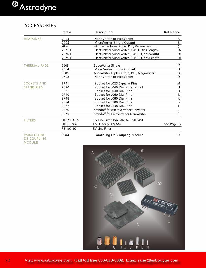
ACCESSORIESecnerefeRnoitpircseD# traP
HEATSINKS AretreVociP ro retreVonaN3002BtuptuO elgniS retreVorciM5002
2006 MicroVerter Triple Output, PFC, MegaVerters 2021LF Heatsink for SuperVerter (1.4” HT, ns Length) 2024LF Heatsink for SuperVerter (0.45” HT, ns Width) 2025LF Heatsink for SuperVerter (0.45” HT, ns Length)
THERMAL PADS 9603 SuperVerter Single DtuptuO elgniS retreVorciM4069
9605 MicroVerter Triple Output, PFC, MegaVertersDretreVociP ro retreVonaN8069
SOCKETS AND MsniP erauqS 520. rof tekcoS1479STANDOFFS IllamS ,sniP ,aiD 040. rof tekcoS0989
HsniP ,aiD 040. rof tekcoS1789LsniP ,aiD 060. rof tekcoS0479KsniP ,aiD 080. rof tekcoS8479GsniP ,aiD 001. rof tekcoS4989FsniP ,aiD 831. rof tekcoS2789
9878 Stando for MicroVerter or UniVerter9528 Stando for PicoVerter or NanoVerter
FILTERS HH-2033-15 SV Line Filter 15A, 50V, MIL STD 461HH-1199-6 EMI Filter (250V, 6A) See Page 35FB-100-10 SV Line Filter
PARALLELING UeludoM gnilpuoC-eD gnilellaraPMDPDE-COUPLING MODULE
E
CD2D1D1
D
D
J
32

Visit www.astrodyne.com. Call toll free 800-823-8082. Email [email protected] 3354
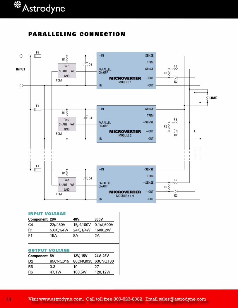
PARALLELING DE-COUPLING MODULE (PDM)MODEL PDM U.S. PATENT NO 5,428,523
DESCRIPTIONThe Paralleling De-Coupling Module isolatesthe parallel pins when multiple modules areconnected in a paralleling, current sharing configuration where redundancy is required.See paralleling connection diagram on page 55.
FEATURES• Isolates Parallel Pin for n+m Redundancy• Provides Fault Tolerance with No Single
Point Of Failure• De-Couples Faulty Module with Minimum
Bus Disturbance• Re-Couples Replacement Module with
Minimum Bus Disturbance During Hot Plug-In• Allows for Individual Module On/Off• Low Impedance for Precise
Current Sharing• Convenient SIP Package
1.34
.12.10
.20 .20
.21
.13
.43
0.025 SQ. x 0.22 PINS5 PL.
.90
TOP VIEW
Visit www.astrodyne.com. Call toll free 800-823-8082. Email [email protected]
-SENSE
TRIM
+SENSE
+OUT
-OUT
+IN
-IN
R1
F1
INPUT
LOAD
PDM
C4 R5
D2
R6
Vcc
SHARE PAR
GND
+
PARALLELON/OFF
MICROVERTERMODULE 1
-SENSE
TRIM
+SENSE
+OUT
-OUT
+IN
-IN
R1
F1
PDM
C4 R5
D2
R6
Vcc
SHARE PAR
GND
+
PARALLELON/OFF
MICROVERTERMODULE n+m
-SENSE
TRIM
+SENSE
+OUT
-OUT
+IN
-IN
R1
F1
PDM
C4 R5
D2
R6
Vcc
SHARE PAR
GND
+
PARALLELON/OFF
MICROVERTERMODULE 2
RO Associates | Tel: 408.744.1450 | Fax: 408.744.1521 | email: [email protected]
55
PARALLELING CONNECTION
INPUT VOLTAGEComponent 28V 48V 300VC4 22µf,50V 15µf,100V 0.1µf,600VR1 5.6K,1/4W 24K,1/4W 160K,2WF1 15A 8A 2A
OUTPUT VOLTAGEComponent 5V 12V, 15V 24V, 28VD2 85CNQ015 80CNQ035 63CNQ100R5 3.3 10 27R6 47,1W 100,5W 120,12W
34
Visit www.astrodyne.com. Call toll free 800-823-8082. Email [email protected]
-SENSE
TRIM
+SENSE
+OUT
-OUT
+IN
-IN
R1
F1
INPUT
LOAD
PDM
C4 R5
D2
R6
Vcc
SHARE PAR
GND
+
PARALLELON/OFF
MICROVERTERMODULE 1
-SENSE
TRIM
+SENSE
+OUT
-OUT
+IN
-IN
R1
F1
PDM
C4 R5
D2
R6
Vcc
SHARE PAR
GND
+
PARALLELON/OFF
MICROVERTERMODULE n+m
-SENSE
TRIM
+SENSE
+OUT
-OUT
+IN
-IN
R1
F1
PDM
C4 R5
D2
R6
Vcc
SHARE PAR
GND
+
PARALLELON/OFF
MICROVERTERMODULE 2
RO Associates | Tel: 408.744.1450 | Fax: 408.744.1521 | email: [email protected]
55
PARALLELING CONNECTION
INPUT VOLTAGEComponent 28V 48V 300VC4 22µf,50V 15µf,100V 0.1µf,600VR1 5.6K,1/4W 24K,1/4W 160K,2WF1 15A 8A 2A
OUTPUT VOLTAGEComponent 5V 12V, 15V 24V, 28VD2 85CNQ015 80CNQ035 63CNQ100R5 3.3 10 27R6 47,1W 100,5W 120,12W
3556
APPLICATION NOTES
INDEX OF SELECTED APPLICATION NOTES
No. Description PageAP1 Module Handling Considerations 57
AP2 Mechanical Mounting Considerations 58
AP5 Output Voltage Trimming 59
AP6 Remote Sensing 67
AP7 Measuring Line and Load Regulation 69
AP8 Measuring Output Noise and Ripple 70
AP10 Thermal Considerations 72
A complete set of Application Notes is available from the factory including the following titles:
AP1 Module Handling Considerations
AP2 Mechanical Mounting Considerations
AP3 Input Ripple Measurement and Filtering
AP4 Logic On-Off
AP5 Output Voltage Trimming
AP6 Remote Sensing
AP7 Measuring Line and Load Regulation
AP8 Measuring Output Noise and Ripple
AP9 Trimming Paralleled Modules
AP10 Thermal Considerations
AP11 Non-Redundant Paralleling of UV300 Modules
AP12 Synchronization of Modules
AP13 Paralleling with Current Sharing and n+m Redundancy
AP14 Special Considerations for MicroVerter Triples
AP18 Board Layout Considerations and Recommendations
AP19 Hole Dimensions and Socket Information
AP20 MTBF Calculations
AP23 PFC Load Restrictions During Startup
AP24 Power Factor Correction (PFC) Modules
AP25 SuperVerter DC-DC Converters
THE LATEST VERSION OF ALL OUR APPLICATIONNOTES ARE AVAILABLE IN PDF FORMAT ON OURWEB SITE OR CALL 800 443-1450 FOR A COMPLETE SET OF PRINTED APPLICATION NOTES

Visit www.astrodyne.com. Call toll free 800-823-8082. Email [email protected]
RO Associates | Tel: 408.744.1450 | Fax: 408.744.1521 | email: [email protected]
57
AP1 MODULE HANDLING CONSIDERATIONS
GENERAL DESCRIPTION
RO DC-DC and AC-DC converter modules have proven to be extremely rugged and aredesigned to meet MIL-STD-810D requirements.Also, once they are installed properly on aprinted circuit board, they can take all the normal mechanical forces for circuit boardsand circuit board mounted components.Reasonable care must exercised, however, during all handling of converter modules, to prevent mechanical damage to the case or the electrical terminal pins.
IMPLEMENTATION
STORAGEModules should be kept in their original ship-ping containers to provide adequate protectionuntil inserted into printed circuit boards.
INSTALLATION INTO PRINTED CIRCUIT BOARDReasonable care must be exercised wheninserting the pins of a module into the holes or sockets of a printed circuit board during production or prototype fabrication. The pinsmust all be properly aligned with the holes orsockets before pressure is evenly exerted tothe surface of the module to seat it onto theboard. Otherwise, overstressed or bent pinscould result in external pin breakage, internaldamage, or degradation of the module.
REMOVAL FROM PRINTED CIRCUIT BOARDIn soldered applications, solder must be carefully removed from the pin/pad connec-tions and each pin must be observed to bemechanically free from its pad. Once the solder is adequately removed, or for socketapplications, the module must be removedusing both hands, one on either end of themodule, to carefully lift the module evenly
off the board. While the pins are clearing thesockets or circuit board holes, the plane of the module baseplate must remain in parallelwith the plane of the circuit board. Otherwise,the pins may be over stressed or bent resultingin degradation or failure.
SHIPMENT OF MODULESIn the event that individual modules areshipped as a component and not in a circuitboard assembly, adequate protection must be provided to the pins to prevent damage.Utilization of the original plastic shipping tube from RO is recommended.
RELATED TOPICS
AP-2 Mechanical Mounting Considerations
AP-18 Board Layout Considerations and Recommendations
AP-19 Hole Dimensions and SocketInformation
36
Visit www.astrodyne.com. Call toll free 800-823-8082. Email [email protected] 3758
GENERAL DESCRIPTION
RO DC-DC and AC-DC converter modules have proven to be extremely rugged, and aredesigned to meet MIL-STD-810D require-ments. Also, once they are installed properlyon a printed circuit board, they can take all thenormal mechanical forces for circuit boardsand circuit board mounted components.Reasonable care must be exercised, however,during the design and fabrication of modulesinto power supply assemblies to preventexcess stress that could cause mechanicaldamage to the case or the electrical terminalpins.
IMPLEMENTATION
DESIGNGood mechanical engineering practices mustbe observed in designing modules into powersupply assemblies to prevent excess stress orbending forces on the modules and their elec-trical terminal pins. Circuit board holes andsockets must be properly located and mechan-ical attachment to heat sinks and circuit boardsmust be designed to prevent excess shear,compression, or tensile forces on the pins.(See AP-19, Hole Dimensions and SocketInformation.)
AP2 MECHANICAL MOUNTING CONSIDERATIONSCONTINUED
ASSEMBLYGood manufacturing procedures must beobserved in assembling modules into powersupply assemblies to prevent excess stress onthe modules or pins. Reasonable care must beexercised in inserting (and removing) modulesfrom printed circuit boards (See AP-1, ModuleHandling Considerations).
In particular, care must be exercised in applications where a single heat sink isattached to more than one module in a sol-dered application. If possible, the heat sinkshould be assembled to the modules prior to soldering. In situations where this is not possible, care must be exercised to insure thatbolting of the modules to the heat sink follow-ing the soldering operation does not result inexcess stress on the pins. One approach mightbe to fixture the modules during soldering toinsure their baseplates are co-planer and toalso insure that the heat sink is flat and that pin forces are reasonable during and afterassembly.
RELATED TOPICS
AP-1 Module Handling Considerations
AP-18 Board Layout Considerations and Recommendations
AP-19 Hole Dimensions and SocketInformation

Visit www.astrodyne.com. Call toll free 800-823-8082. Email [email protected]
RO Associates | Tel: 408.744.1450 | Fax: 408.744.1521 | email: [email protected]
59
AP5 OUTPUT VOLTAGE TRIMMING
GENERAL DESCRIPTION
Output voltage trimming allows the user to change the output voltage of the module. This greatly enhances the functionality of modules by allowing a few select, standardmodules to be applied to virtually any applica-tion; regardless of the voltage requirements.This allows module users to reduce the number of models kept in stock.
This application note covers the basics of trimming all RO modules available as of June2002. The format of the trim equation has beenmodi fied so that a single trimming equationcan be used. The equation parameters for aparticular module can be found in the relevantparameters table.
PageQUATTROVERTER Trimming Parameters 59SYNCROVERTER Trimming Parameters 60SUPERVERTER DUAL Trimming Parameters 61SUPERVERTER Trimming Parameters 61PICOVERTER Trimming Parameters 62MICROVERTER Trimming Parameters 63MEGAVERTER Trimming Parameters 63NANOVERTER Trimming Parameters 64
Also covered, are the effects of trimming onvarious performance parameters, applicationideas for trimming, and important precautionsto observe.
IMPLEMENTATION
BASIC TRIMMING CONCEPTSRO uses a simple approach to trimming modules that in most cases allows the moduleto be trimmed with a single external resistor.There are two types of trimming used in ROmodules: Inverting trim, in which the trim signalis summed in with the sense feedback andNon-inverting trim, in which the trim signal isused to modify the reference for the controlcircuits. In either case, to trim the module's
output connect a resistor from TRIM to either+SENSE or -SENSE depending on whetheryou want a lower or higher than nominal output voltage and which type of trimming themodule uses. Each of the following parametertables indicates which type of trimming is usedby the module, whether to connect to +SENSEor –SENSE, and the parameter values to enterin the trim equation. The figures accompanyingthe tables show the appropriate connections.
To calculate the resistor value use the following equation:
Where:
A and B = The equation parameters given in the tables.
| ∆V| = The magnitude of the desired voltagechange from the nominal output voltage. | ∆V| is always positive.
QUATTROVERTER TRIMMINGThe trimming parameters for the QUATTROVERTER modules are given in Table 5a. These parameters, along with thedesired change in output voltage are pluggedinto the trim resistor equation:
The QUATTROVERTER modules use a non-inverting trim function. To trim the output volt-age UP, connect the trim resistor from TRIM to+SENSE. To trim the output voltage DOWN ,connect the trim resistor from TRIM to -SENSE.These connections are shown in Figure 5a.
38

Visit www.astrodyne.com. Call toll free 800-823-8082. Email [email protected]
RO Associates | Tel: 408.744.1450 | Fax: 408.744.1521 | email: [email protected]
59
AP5 OUTPUT VOLTAGE TRIMMING
GENERAL DESCRIPTION
Output voltage trimming allows the user to change the output voltage of the module. This greatly enhances the functionality of modules by allowing a few select, standardmodules to be applied to virtually any applica-tion; regardless of the voltage requirements.This allows module users to reduce the number of models kept in stock.
This application note covers the basics of trimming all RO modules available as of June2002. The format of the trim equation has beenmodi fied so that a single trimming equationcan be used. The equation parameters for aparticular module can be found in the relevantparameters table.
PageQUATTROVERTER Trimming Parameters 59SYNCROVERTER Trimming Parameters 60SUPERVERTER DUAL Trimming Parameters 61SUPERVERTER Trimming Parameters 61PICOVERTER Trimming Parameters 62MICROVERTER Trimming Parameters 63MEGAVERTER Trimming Parameters 63NANOVERTER Trimming Parameters 64
Also covered, are the effects of trimming onvarious performance parameters, applicationideas for trimming, and important precautionsto observe.
IMPLEMENTATION
BASIC TRIMMING CONCEPTSRO uses a simple approach to trimming modules that in most cases allows the moduleto be trimmed with a single external resistor.There are two types of trimming used in ROmodules: Inverting trim, in which the trim signalis summed in with the sense feedback andNon-inverting trim, in which the trim signal isused to modify the reference for the controlcircuits. In either case, to trim the module's
output connect a resistor from TRIM to either+SENSE or -SENSE depending on whetheryou want a lower or higher than nominal output voltage and which type of trimming themodule uses. Each of the following parametertables indicates which type of trimming is usedby the module, whether to connect to +SENSEor –SENSE, and the parameter values to enterin the trim equation. The figures accompanyingthe tables show the appropriate connections.
To calculate the resistor value use the following equation:
Where:
A and B = The equation parameters given in the tables.
| ∆V| = The magnitude of the desired voltagechange from the nominal output voltage. | ∆V| is always positive.
QUATTROVERTER TRIMMINGThe trimming parameters for the QUATTROVERTER modules are given in Table 5a. These parameters, along with thedesired change in output voltage are pluggedinto the trim resistor equation:
The QUATTROVERTER modules use a non-inverting trim function. To trim the output volt-age UP, connect the trim resistor from TRIM to+SENSE. To trim the output voltage DOWN ,connect the trim resistor from TRIM to -SENSE.These connections are shown in Figure 5a.
39
+ OUT
+ SENSE
TRIM
– SENSE
– OUT
TRIM-DOWN
+ OUT
+ SENSE
TRIM
– SENSE
– OUT
TRIM-UP
LOAD
LOADRtrim-up
Rtrim-dn
+ OUT
+ SENSE
TRIM
– SENSE
– OUT
TRIM-DOWN
+ OUT
+ SENSE
TRIM
– SENSE
– OUT
TRIM-UP
LOAD
LOADRtrim-up
Rtrim-dn
60
Model V nom Trim up Trim down Min. Max.Suffix (V) A B A B Vout Vout
-1.8 1.8 4.154 -2.802 9.198 -10.22 1.44 1.98
-2.5 2.5 12.98 .08242 12.78 -10.22 2.00 2.75
-3.3 3.3 28.01 3.379 16.86 -10.22 2.64 3.63
-5 5.0 77.47 10.38 25.55 -10.22 4 5.5
Table 5a QUATTROVERTER Trimming Parameters.(Connections shown in Figure 5a).
Example: An application requires 26.5A at1.90V to drive a DSP based voice messagingsystem. In this application we will use the “–30”version of the 1.8V QuattroVerter module, whichhas a current rating of 30A and is perfect for thisapplication. The required trim resistor is:
For our application we will use a 38.3 k Ω, 1%, temperature stable, SMT chip resistor connected from TRIM to +SENSE.
Figure 5a Basic circuits for QUATTROVERTER trim-up and trim-down applications.
TRIMMINGThe trimming parameters are given in Table 5b. These parameters, along with thedesired change in output voltage are pluggedinto the trim resistor equation:
The modules use a non-inverting trim function.To trim the voltage UP, connect the trim resistor from TRIM to +SENSE. To trim the output voltage
,DOWN connect the trim resistor from TRIM to -SENSE.These connections are shown in Figure 5b.
Model Vnom Trim Up Trim Down Min. Max. Suffix (V) A B A B Vout Vout
-1.8 1.8 .8129 -.5484 1.8 -2 1.44 1.98
-2.5 2.5 2.540 .01613 2.5 -2 2.00 2.75
-3.3 3.3 5.482 .6613 3.3 -2 2.64 3.63
-5 5.0 15.16 2.032 5.0 -2 4 5.5
Table 5b Trimming Parameters.(Connections shown in Figure 5b).
Example: An application requires 39A at 2.1V topower a processor in an internet router. In thisapplication we will use the “–45” version of the2.5V SyncroVerter module. This 2.5V modulehas a current rating of 45A, which is sufficientfor this application. The required trim resistor is:
For our application we will use a 4.22 k Ω, 1%, temperature stable, SMT chip resistor connect-ed from TRIM to -SENSE.
Figure 5b Basic circuits for trim-up and trim-down applications.
AP5 OUTPUT VOLTAGE TRIMMING CONTINUED

Visit www.astrodyne.com. Call toll free 800-823-8082. Email [email protected]
R trim= 16.71xk Ω
R trim= 6.350 – 15.04x | 0.2 |
xk Ω| 0.2 |
LOAD
Rtrim-dnLOAD
Rtrim-up
+ OUT
+ SENSE
TRIM
– SENSE
– OUT
TRIM - DOWN
+ OUT
+ SENSE
TRIM
– SENSE
– OUT
TRIM -UP
RO Associates | Tel: 408.744.1450 | Fax: 408.744.1521 | email: [email protected]
61
SUPERVERTER DUAL TRIMMINGThe trimming parameters for the SUPERVERTER DUAL modules are given in Table 5c. These parameters, along with the desired change in output voltage are plugged into the trim resistor equation:
The SUPERVERTER DUAL modules use aninverting trim function. To trim the output voltage UP , connect the trim resistor fromTRIM to -SENSE. To trim the output voltageDOWN , connect the trim resistor from TRIM to +SENSE. These connections areshown in Figure 5c.
Output Vnom Trim up Trim down Min. Max.# (V) A B A B Vout Vout
2 1.8 1.250 -5.110 .5645 -6.118 1.62 1.98
2 2.5 6.250 -10.00 6.350 -15.04 2.25 2.75
1 3.3 2.069 -5.110 3.437 -6.779 2.97 3.63
2 3.3 .8000 -.3650 .2560 -.6850 2.97 3.63
1 5 2.508 -3.320 2.508 -4.323 4.5 5.5
Table 5c SUPERVERTER DUAL Trimming Parameters.(Connections shown in Figure 5c).
Example: An application requires 12A at 2.3Vto drive a processor core and 3.3V at 8A todrive the peripheral I/O. In this application wewill use the 3.3V/ 2.5V SUPERVERTER DUALmodule. Both outputs are within their respec-tive current rating and are acceptable for thisapplication. We need to trim the 2.5V outputdown to 2.3V. The 2.5V output is output #2 onthe SVD48-3325 module so the required trim resistor is:
For our application we will use a 16.9kΩ, 1%, temperature stable, SMT chip resistor connected from TRIM to -SENSE.
Figure 5cBasic circuits for SUPERVERTER DUAL trim-up and trim-down applications.
SUPERVERTER TRIMMINGThe trimming parameters for the SUPERVERTER modules are given in Table 5d.These parameters, along with the desiredchange in output voltage are plugged into the trim resistor equation:
The SUPERVERTER modules use a non-inverting trim function. To trim the output voltage UP , connect the trim resistor from TRIMto +SENSE. To trim the output voltage DOWN ,connect the trim resistor from TRIM to -SENSE.These connections are shown in Figure 5d.
Model Vnom Trim up Trim down Min. Max.Suffix (V) A B A B Vout Vout
-2.5 2.5 2.540 0.01613 2.5 -2 1.5 2.75
-3.3 3.3 5.482 0.6613 3.3 -2 1.98 3.63
-5 5 15.16 2.032 5 -2 3.00 5.5
-12 12 104.1 7.677 12 -2 7.20 13.2
-15 15 166.5 10.10 15 - 9.00 16.5
-24 24 440.5 17.35 24 -2 14.4 26.4
-28 28 604.3 20.58 28 -2 16.8 30.8
Table 5dSUPERVERTER Trimming Parameters.(Connections shown in Figure 5d).
40

Visit www.astrodyne.com. Call toll free 800-823-8082. Email [email protected]
R trim= 16.71xk Ω
R trim= 6.350 – 15.04x | 0.2 |
xk Ω| 0.2 |
LOAD
Rtrim-dnLOAD
Rtrim-up
+ OUT
+ SENSE
TRIM
– SENSE
– OUT
TRIM - DOWN
+ OUT
+ SENSE
TRIM
– SENSE
– OUT
TRIM -UP
RO Associates | Tel: 408.744.1450 | Fax: 408.744.1521 | email: [email protected]
61
SUPERVERTER DUAL TRIMMINGThe trimming parameters for the SUPERVERTER DUAL modules are given in Table 5c. These parameters, along with the desired change in output voltage are plugged into the trim resistor equation:
The SUPERVERTER DUAL modules use aninverting trim function. To trim the output voltage UP , connect the trim resistor fromTRIM to -SENSE. To trim the output voltageDOWN , connect the trim resistor from TRIM to +SENSE. These connections areshown in Figure 5c.
Output Vnom Trim up Trim down Min. Max.# (V) A B A B Vout Vout
2 1.8 1.250 -5.110 .5645 -6.118 1.62 1.98
2 2.5 6.250 -10.00 6.350 -15.04 2.25 2.75
1 3.3 2.069 -5.110 3.437 -6.779 2.97 3.63
2 3.3 .8000 -.3650 .2560 -.6850 2.97 3.63
1 5 2.508 -3.320 2.508 -4.323 4.5 5.5
Table 5c SUPERVERTER DUAL Trimming Parameters.(Connections shown in Figure 5c).
Example: An application requires 12A at 2.3Vto drive a processor core and 3.3V at 8A todrive the peripheral I/O. In this application wewill use the 3.3V/ 2.5V SUPERVERTER DUALmodule. Both outputs are within their respec-tive current rating and are acceptable for thisapplication. We need to trim the 2.5V outputdown to 2.3V. The 2.5V output is output #2 onthe SVD48-3325 module so the required trim resistor is:
For our application we will use a 16.9kΩ, 1%, temperature stable, SMT chip resistor connected from TRIM to -SENSE.
Figure 5cBasic circuits for SUPERVERTER DUAL trim-up and trim-down applications.
SUPERVERTER TRIMMINGThe trimming parameters for the SUPERVERTER modules are given in Table 5d.These parameters, along with the desiredchange in output voltage are plugged into the trim resistor equation:
The SUPERVERTER modules use a non-inverting trim function. To trim the output voltage UP , connect the trim resistor from TRIMto +SENSE. To trim the output voltage DOWN ,connect the trim resistor from TRIM to -SENSE.These connections are shown in Figure 5d.
Model Vnom Trim up Trim down Min. Max.Suffix (V) A B A B Vout Vout
-2.5 2.5 2.540 0.01613 2.5 -2 1.5 2.75
-3.3 3.3 5.482 0.6613 3.3 -2 1.98 3.63
-5 5 15.16 2.032 5 -2 3.00 5.5
-12 12 104.1 7.677 12 -2 7.20 13.2
-15 15 166.5 10.10 15 - 9.00 16.5
-24 24 440.5 17.35 24 -2 14.4 26.4
-28 28 604.3 20.58 28 -2 16.8 30.8
Table 5dSUPERVERTER Trimming Parameters.(Connections shown in Figure 5d).
41
Rtrim = 65.76xkΩ
Rtrim = 259.6 –20.77x| 3|xkΩ
| 3|
Rtrim = 4.00xkΩ
Rtrim = 12.000 –2x| 2|xkΩ
| 2|
+ OUT
+ SENSE
TRIM
– SENSE
– OUT
TRIM-DOWN
+ OUT
+ SENSE
TRIM
– SENSE
– OUT
TRIM-UP
LOAD
LOADRtrim-up
R trim-dn
LOAD
Rtrim-dnLOAD
Rtrim-up
+ OUT
+ SENSE
TRIM
– SENSE
– OUT
TRIM-DOWN
+ OUT
+ SENSE
TRIM
– SENSE
– OUT
TRIM-UP
62
Example: An application requires 11.5A at 10Vto drive a cooling system for a super conductingRF receiver-fi lter in a cellular base station. In thisapplication we will use the –150 version of a 12V SuperVerter module. The 12V module has a current rating of 12.5A, which is good for thisapplication. The required trim resistor is:
For our application we will use a 4.02 Ω, 1%, temperature stable, SMT chip resistor connected from TRIM to -SENSE.
Figure 5d Basic circuits for SUPERVERTER trim-up andtrim-down applications.
PICOVERTER TRIMMINGThe trimming parameters for the PICOVERTER modules are given in Table 5e.These parameters, along with the desiredchange in output voltage are plugged into the trim resistor equation:
The PICOVERTER modules use an invertingtrim function. To trim the output voltage UP,connect the trim resistor from TRIM to–SENSE. To trim the output voltage DOWN,connect the trim resistor from TRIM to+SENSE. These connections are shown in Figure 5e.
Model Vnom Trim up Trim down Min. Max.Suffix (V) A B A B Vout Vout
-3 3.3 1.986 0 3.300 -1.602 2.97 3.63
-5 5 12.58 0 12.58 -5.030 4.5 5.5
-12 12 41.80 0 158.8 -16.72 10.8 13.2
-15 15 51.92 0 259.6 -20.77 13.5 16.5
-24 24 104.4 0 897.9 -41.76 21.6 26.4
Table 5e PICOVERTER Trimming Parameters(Connections shown in Figure 5e).
Example: A designer has a system that usesboth 12V and 15V PICOVERTER modules. Shewould like to minimize part count and lowercost by only using one model of thePICOVERTER series. By checking with the factory she learned that the 15V PICOVERTERmodule can be trimmed down to 12V and stillhandle the modest load requirements. The required trim down resistor is:
She used a 66.5kΩ, 1%, temperature stable,metal fi lm resistor for the trim down resistorand connect it from TRIM to +SENSE.
Figure 5e Basic circuits for PICOVERTER trim-up and trim-down applications.
AP5 OUTPUT VOLTAGE TRIMMING CONTINUED
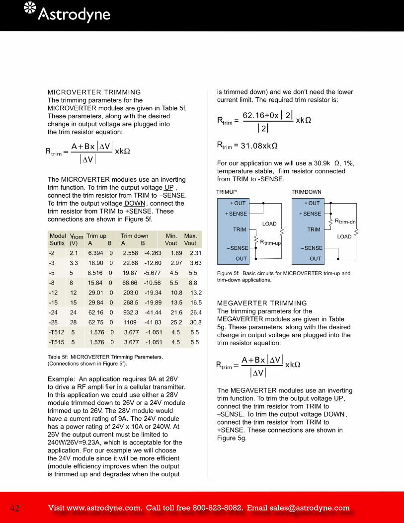
Visit www.astrodyne.com. Call toll free 800-823-8082. Email [email protected]
Rtrim = 31.08xkΩ
Rtrim = 62.16+0x | 2|xkΩ
| 2|
LOAD
Rtrim-dnLOAD
Rtrim-up
+ OUT
+ SENSE
TRIM
– SENSE
– OUT
TRIM-DOWN
+ OUT
+ SENSE
TRIM
– SENSE
– OUT
TRIM-UP
RO Associates | Tel: 408.744.1450 | Fax: 408.744.1521 | email: [email protected]
63
MICROVERTER TRIMMINGThe trimming parameters for the MICROVERTER modules are given in Table 5f.These parameters, along with the desiredchange in output voltage are plugged into the trim resistor equation:
The MICROVERTER modules use an invertingtrim function. To trim the output voltage UP ,connect the trim resistor from TRIM to –SENSE.To trim the output voltage DOWN, connect thetrim resistor from TRIM to +SENSE. Theseconnections are shown in Figure 5f.
Model Vnom Trim up Trim down Min. Max.Suffix (V) A B A B Vout Vout
-2 2.1 6.394 0 2.558 -4.263 1.89 2.31
-3 3.3 18.90 0 22.68 -12.60 2.97 3.63
-5 5 8.516 0 19.87 -5.677 4.5 5.5
-8 8 15.84 0 68.66 -10.56 5.5 8.8
-12 12 29.01 0 203.0 -19.34 10.8 13.2
-15 15 29.84 0 268.5 -19.89 13.5 16.5
-24 24 62.16 0 932.3 -41.44 21.6 26.4
-28 28 62.75 0 1109 -41.83 25.2 30.8
-T512 5 1.576 0 3.677 -1.051 4.5 5.5
-T515 5 1.576 0 3.677 -1.051 4.5 5.5
Table 5f: MICROVERTER Trimming Parameters.(Connections shown in Figure 5f).
Example: An application requires 9A at 26V to drive a RF ampli fier in a cellular transmitter.In this application we could use either a 28Vmodule trimmed down to 26V or a 24V moduletrimmed up to 26V. The 28V module wouldhave a current rating of 9A. The 24V modulehas a power rating of 24V x 10A or 240W. At26V the output current must be limited to 240W/26V=9.23A, which is acceptable for the application. For our example we will choosethe 24V module since it will be more efficient(module efficiency improves when the outputis trimmed up and degrades when the output
is trimmed down) and we don't need the lowercurrent limit. The required trim resistor is:
For our application we will use a 30.9k Ω, 1%, temperature stable, fi lm resistor connectedfrom TRIM to -SENSE.
Figure 5f: Basic circuits for MICROVERTER trim-up andtrim-down applications.
MEGAVERTER TRIMMINGThe trimming parameters for the MEGAVERTER modules are given in Table 5g. These parameters, along with the desiredchange in output voltage are plugged into thetrim resistor equation:
The MEGAVERTER modules use an invertingtrim function. To trim the output voltage UP,connect the trim resistor from TRIM to–SENSE. To trim the output voltage DOWN ,connect the trim resistor from TRIM to+SENSE. These connections are shown in Figure 5g.
42

Visit www.astrodyne.com. Call toll free 800-823-8082. Email [email protected] 43
Rtrim = 1.969xkΩ
Rtrim = 1.438–0.9070x| 0.5| xkΩ| 0.5|
Rtrim = 490xkΩ
Rtrim = 1023–21.79x| 2|xkΩ
| 2|
LOAD
Rtrim-dnLOAD
Rtrim-up
+ OUT
+ SENSE
TRIM
– SENSE
– OUT
TRIM-DOWN
+ OUT
+ SENSE
TRIM
– SENSE
– OUT
TRIM-UP
64
Model Vnom Trim up Trim down Min. Max.Suffix (V) A B A B Vout Vout
MV48-5 5 3.549 0 10.76 -2.862 4.5 5.5
MV48-26 26 32.76 -2.67 308.0 -15.78 18** 30
MV380-26 26 32.76 -2.67 308.0 -15.78 18** 30
MV380-48 48 40.56 -2.67 738.2 -18.89 40 51
MV380-56 56 47.81 -2.67 1023 -21.79 48 60
**Minimum load conditions apply below 20V out. See the data sheet.
Table 5g: MEGAVERTER Trimming Parameters.(Connections shown in Figure 5g).
Example: An application requires 18A at 24V to drive a microwave ampli fier in a communica-tions data link. In this application we will use a26V MegaVerter module trimmed down to 24V.The required trim resistor is:
For our application we will use a 487k Ω, 1%, temperature stable, fi lm resistor connectedfrom TRIM to +SENSE.
Figure 5g: Basic circuits for MEGAVERTER trim-up andtrim-down applications.
NANOVERTER TRIMMINGThe trimming parameters for the NANOVERTER modules are given in Table 5h.These parameters, along with the desiredchange in output voltage are plugged into the trim resistor equation:
The NANOVERTER modules use an invertingtrim function. To trim the output voltage UP ,connect the trim resistor from TRIM to –SENSE.To trim the output voltage DOWN , connect thetrim resistor from TRIM to +SENSE. Theseconnections are shown in Figure 5h.
Model Vnom Trim up Trim down Min. Max.Suffix (V) A B A B Vout Vout
-2 2.1 0.2778 -.3320 .01389 -.4709 2.00 2.21
-3 3.3 0.7424 -.3320 .2376 -.6290 2.97 3.47
-5 5 1.438 -.3320 1.438 -.9070 4.5 5.5
-12 12 3.186 -.3320 12.11 -1.607 10.8 13.2
-15 15 3.354 -.3320 16.77 -1.674 13.5 16.5
-24 24 6.876 -.3320 59.13 -3.082 21.6 26.4
Table 5h: NANOVERTER Trimming Parameters.(Connections shown in Figure 5h).
Example: A 5V logic system needs the capability to perform margin testing. The margin limits are 4.5V and 5.5V. The requiredtrim DOWN resistor is:
AP5 OUTPUT VOLTAGE TRIMMINGCONTINUED

Visit www.astrodyne.com. Call toll free 800-823-8082. Email [email protected]
Rtrim = 2.544xkΩ
Rtrim = 1.438–0.3320x| 0.5| xkΩ| 0.5|
+ OUT+ SENSE
TRIM
– SENSE– OUT
LOAD
Rtrim-up
Rtrim-dn
LOAD
Rtrim-dnLOAD
Rtrim-up
+ OUT
+ SENSE
TRIM
– SENSE
– OUT
TRIM-DOWN
+ OUT
+ SENSE
TRIM
– SENSE
– OUT
TRIM-UP
RO Associates | Tel: 408.744.1450 | Fax: 408.744.1521 | email: [email protected]
65
The required trim UP resistor is:
For this example we will use a 1.96k Ω, 1%, temperature stable, SMT chip for the trimdown resistor and a 2.55k Ω, 1% temperaturestable, SMT chip for the trim up resistor. SeeFigure 5i for the example schematic.
Figure 5h: Basic circuits for NANOVERTER trim-up andtrim-down applications.
Figure 5i: Circuit for NANOVERTER trimming example:Voltage margining using a switch.
PERFORMANCE EFFECTS OF OUTPUT TRIMMING
Several of the module performance parameterswill change as the output voltage is trimmed.All speci fications given in the data sheets apply over the guaranteed adjustment range.The specifications of primary concern are: efficiency, output ripple, and output OVP.
Efficiency – The efficiency of a given model will decrease as the output voltage is trimmeddown and increase as the voltage is trimmedup.
Output Ripple – As a percentage of the outputvoltage, the output ripple will increase as thevoltage is lowered and decrease as the voltageis raised.
Output OVP – The OVP set point remains at afixed voltage, independent of output trimming.In most cases the OVP set point is what limitsthe maximum trimmable voltage.
As an additional note the user must pay attention to the current and power ratingswhen trimming the output voltage. All RO converters have a fixed current limit. As theoutput voltage is trimmed down the currentlimit set point remains constant. Therefore, interms of output power, if the unit is trimmeddown the available output power drops proportionally. Likewise, if the output istrimmed up the available power appears to go up, however, do not exceed the maximumrated output power of the module when trimming the output up.
44

Visit www.astrodyne.com. Call toll free 800-823-8082. Email [email protected] 4566
POSSIBLE APPLICATIONS
Eliminating the need for remote sense – Output trimming can be used instead ofremote sense when the load current change is limited and the voltage drop between converter and load is relatively constant.
System testing (margining) – Often, it’s helpfulto test system operation with the supply voltage – usually the +5V logic voltage – setfirst at one extreme, then at the other. Any circuitry that fails to perform properly underthese manufacturer's test conditions might also fail under conditions found in the user'senvironment. Margin testing helps insure trouble-free system operation.
Obtaining non-standard output voltages –When a non-standard output voltage is necessary, it may be available simply by trimming the output voltage of a module withan output voltage that's close to the desiredvoltage. Although the published data sheet limits are valid for the guaranteed adjustmentrange, lower output voltages are commonlyavailable by using the trim function. Contactthe factory for details.
Reducing the number of stocked models –When two output voltages are necessary, such as 24V and 28V, one model may be ableto supply both, using the trim function to setthe lower voltage.
PRECAUTIONS
Connect trim resistor to sense, not to output –The trim resistor(s) should be connected to the sense leads, not to the output leads or tothe load. Otherwise, load current changescould cause the converter’s trimmed outputvoltage to vary.
Noise sensitivity – The TRIM pin is noise sensitive. External resistors (either fixed orvariable) should be located within one cm ofthe converter. If wires are necessary, use twisted or shielded wires.
Output power, output current – If the output voltage is increased, output currentmust be derated to avoid exceeding modulemaximum output power. If the output voltageis decreased, output current is limited to itsmaximum rating and the available outputpower decreases.
Adjustment range limits – In some cases, theoutput voltage can be trimmed outside theguaranteed adjustment range. However, datasheet specifications are only valid within thespecified voltage range.
RELATED TOPICS
AP-6 Remote Sensing
AP-9 Trimming Paralleled Modules
AP-18 Board Layout Considerations and Recommendations
AP5 OUTPUT VOLTAGE TRIMMINGCONTINUED
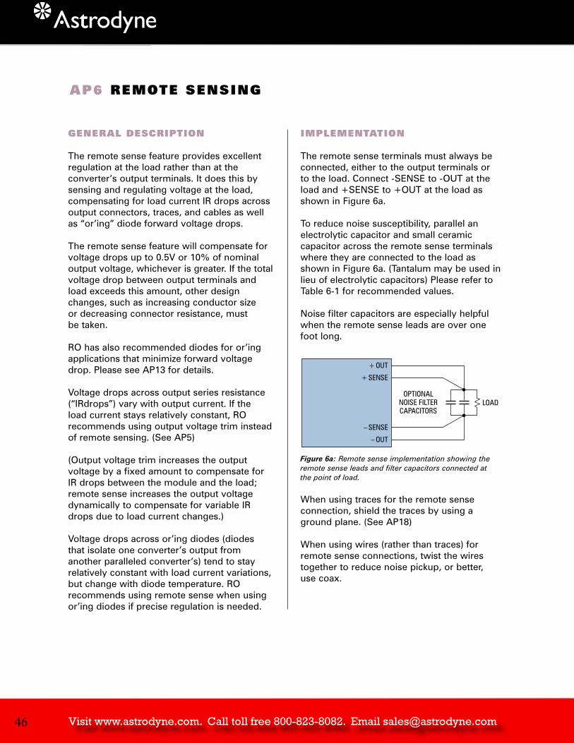
Visit www.astrodyne.com. Call toll free 800-823-8082. Email [email protected]
+ OUT
+ SENSE
– SENSE
– OUT
LOADOPTIONAL
NOISE FILTERCAPACITORS
RO Associates | Tel: 408.744.1450 | Fax: 408.744.1521 | email: [email protected]
67
AP6 REMOTE SENSING
GENERAL DESCRIPTION
The remote sense feature provides excellentregulation at the load rather than at theconverter’s output terminals. It does this bysensing and regulating voltage at the load,compensating for load current IR drops acrossoutput connectors, traces, and cables as wellas “or’ing” diode forward voltage drops.
The remote sense feature will compensate forvoltage drops up to 0.5V or 10% of nominaloutput voltage, whichever is greater. If the totalvoltage drop between output terminals andload exceeds this amount, other designchanges, such as increasing conductor size or decreasing connector resistance, must be taken.
RO has also recommended diodes for or’ingapplications that minimize forward voltagedrop. Please see AP13 for details.
Voltage drops across output series resistance(“IRdrops”) vary with output current. If the load current stays relatively constant, RO recommends using output voltage trim insteadof remote sensing. (See AP5)
(Output voltage trim increases the output voltage by a fixed amount to compensate forIR drops between the module and the load;remote sense increases the output voltagedynamically to compensate for variable IRdrops due to load current changes.)
Voltage drops across or’ing diodes (diodes that isolate one converter’s output from another paralleled converter’s) tend to stay relatively constant with load current variations,but change with diode temperature. RO recommends using remote sense when usingor’ing diodes if precise regulation is needed.
IMPLEMENTATION
The remote sense terminals must always beconnected, either to the output terminals or to the load. Connect -SENSE to -OUT at theload and +SENSE to +OUT at the load asshown in Figure 6a.
To reduce noise susceptibility, parallel anelectrolytic capacitor and small ceramic capacitor across the remote sense terminalswhere they are connected to the load asshown in Figure 6a. (Tantalum may be used inlieu of electrolytic capacitors) Please refer toTable 6-1 for recommended values.
Noise filter capacitors are especially helpfulwhen the remote sense leads are over one foot long.
Figure 6a: Remote sense implementation showing theremote sense leads and filter capacitors connected at the point of load.
When using traces for the remote sense connection, shield the traces by using a ground plane. (See AP18)
When using wires (rather than traces) forremote sense connections, twist the wirestogether to reduce noise pickup, or better, use coax.
46

Visit www.astrodyne.com. Call toll free 800-823-8082. Email [email protected]
+ OUT
+ SENSE
– SENSE
– OUT
LOADOPTIONAL
NOISE FILTERCAPACITORS
RO Associates | Tel: 408.744.1450 | Fax: 408.744.1521 | email: [email protected]
67
AP6 REMOTE SENSING
GENERAL DESCRIPTION
The remote sense feature provides excellentregulation at the load rather than at theconverter’s output terminals. It does this bysensing and regulating voltage at the load,compensating for load current IR drops acrossoutput connectors, traces, and cables as wellas “or’ing” diode forward voltage drops.
The remote sense feature will compensate forvoltage drops up to 0.5V or 10% of nominaloutput voltage, whichever is greater. If the totalvoltage drop between output terminals andload exceeds this amount, other designchanges, such as increasing conductor size or decreasing connector resistance, must be taken.
RO has also recommended diodes for or’ingapplications that minimize forward voltagedrop. Please see AP13 for details.
Voltage drops across output series resistance(“IRdrops”) vary with output current. If the load current stays relatively constant, RO recommends using output voltage trim insteadof remote sensing. (See AP5)
(Output voltage trim increases the output voltage by a fixed amount to compensate forIR drops between the module and the load;remote sense increases the output voltagedynamically to compensate for variable IRdrops due to load current changes.)
Voltage drops across or’ing diodes (diodes that isolate one converter’s output from another paralleled converter’s) tend to stay relatively constant with load current variations,but change with diode temperature. RO recommends using remote sense when usingor’ing diodes if precise regulation is needed.
IMPLEMENTATION
The remote sense terminals must always beconnected, either to the output terminals or to the load. Connect -SENSE to -OUT at theload and +SENSE to +OUT at the load asshown in Figure 6a.
To reduce noise susceptibility, parallel anelectrolytic capacitor and small ceramic capacitor across the remote sense terminalswhere they are connected to the load asshown in Figure 6a. (Tantalum may be used inlieu of electrolytic capacitors) Please refer toTable 6-1 for recommended values.
Noise filter capacitors are especially helpfulwhen the remote sense leads are over one foot long.
Figure 6a: Remote sense implementation showing theremote sense leads and filter capacitors connected at the point of load.
When using traces for the remote sense connection, shield the traces by using a ground plane. (See AP18)
When using wires (rather than traces) forremote sense connections, twist the wirestogether to reduce noise pickup, or better, use coax.
4768
Figure 6b: When there is a possibility of remotesense leads failing open, connect a 20 Ω resistorfrom each SENSE terminal to its respective OUTterminal at the converter. Also shown is anoptional or'ing diode used when paralleling two ormore converters.
RELATED TOPICS
AP-5 Output Voltage Trimming
AP-7 Measuring Line and Load Regulation
AP-13 Paralleling with Current Sharing and n+m Redundancy
AP-18 Board Layout Considerations andRecommendations
+ OUT+ SENSE
– SENSE– OUT
LOADOPTIONAL
NOISE FILTERCAPACITORS
SUGGESTED FILTER CAPACITOR VALUESVout Electrolytic Tantalum Ceramic
Capacitor in lieu of Capacitorelectrolytic
2.1V, 3.3V 4700µF, 6V 330µF, 6V 0.47µF, Z5U
5.0V 2200µF, 10V 220µF, 10V 0.47µF, Z5U
8.0V 1500µF, 16V 150µF, 15V 0.47µF, Z5U
12V, 15V 1000µF, 35V 68µF, 25V 0.47µF, Z5U
24V, 28V 470µF, 50V 22µF, 50V 0.47µF, Z5U
Table 6-1: Recommended capacitor values forreducing remote sense noise susceptibility.
Although available on all models, remote senseis most useful for high current (low voltage)models,where the potential IR drops are higher.
PRECAUTIONS
Improper use of the remote sense feature canintroduce noise into the module’s feedbackloop, resulting in output noise or oscillations.There are several ways to minimize remotesense lead noise pickup.
(a) Use shielded and/or twisted leads for remotesensing. Also consider using coax cable.
(b) Use noise fi lter capacitors connected acrossthe remote sense leads at the load. See Figure6a and Table 6-1 for further information.
(c) Use output voltage trim to make up for IR drops instead of remote sense if the loadcurrent does not change appreciably. (See AP5)
If the sense leads fail open circuit, the moduleoutput voltage will rise to the OVP set point. Ifthere is any possibility of this situation, connecta 100W resistor from +OUT to +SENSE, andfrom -OUT to -SENSE.
Be careful not to reverse the sense leads. If reversed, the module will be damaged. Astrodyne recommends using keyed connectors.
AP6 REMOTE SENSING CONTINUED

Visit www.astrodyne.com. Call toll free 800-823-8082. Email [email protected]
+ OUT+ SENSE
– SENSE– OUT
+ IN
– IN
V R
I
+ OUT+ SENSE
– SENSE– OUT
+ IN
– IN
VV R
RO Associates | Tel: 408.744.1450 | Fax: 408.744.1521 | email: [email protected]
69
AP7 MEASURING LINE AND LOAD REGULATION
GENERAL DESCRIPTION
Line regulation is the module’s ability to maintain a constant output voltage as the line(input) voltage changes. Load regulation is the module’s ability to maintain a constant outputvoltage as the load current changes.
Line and load regulation are two of the mostcommon types of converter measurements.Although straightforward, there are some simple guidelines that will help insure accuratereadings.
To check the module for regulation, measurethe output voltage at the sense pins (+SENSEand -SENSE). There is virtually no current flowing through the sense leads, and consequently no appreciable drop acrossthem. Therefore, measuring at the sense pinsis equivalent to measuring at the point wherethe sense leads are connected to the outputleads.
In contrast, there can be a significant voltagedrop between the module’s output terminalsand the load. This voltage drop, which varieswith load current, can cause erroneous regulation values. The remote sense terminalsshould always be connected to the outputeither at the output terminals or at the load.(Connect -SENSE to -OUT and +SENSE to+OUT.)
Line Regulation: Connect a DVM to the sense terminals. Vary the input voltage fromminimum to maximum. The output voltagechange, as a percentage of nominal outputvoltage, is the line regulation. See Figure 7a.
Figure 7a: Detail of line (input) regulationmeasurement circuit
Load Regulation: Connect a DVM to the senseterminals. Vary the load current from zero tomaximum. The output voltage change, as apercentage of nominal output voltage, is theload regulation. See Figure 7b.
Figure 7b: Detail of load regulation measurement circuit
48

Visit www.astrodyne.com. Call toll free 800-823-8082. Email [email protected]
+ OUT+ SENSE
– SENSE– OUT
+ IN
– IN
V R
I
+ OUT+ SENSE
– SENSE– OUT
+ IN
– IN
VV R
RO Associates | Tel: 408.744.1450 | Fax: 408.744.1521 | email: [email protected]
69
AP7 MEASURING LINE AND LOAD REGULATION
GENERAL DESCRIPTION
Line regulation is the module’s ability to maintain a constant output voltage as the line(input) voltage changes. Load regulation is the module’s ability to maintain a constant outputvoltage as the load current changes.
Line and load regulation are two of the mostcommon types of converter measurements.Although straightforward, there are some simple guidelines that will help insure accuratereadings.
To check the module for regulation, measurethe output voltage at the sense pins (+SENSEand -SENSE). There is virtually no current flowing through the sense leads, and consequently no appreciable drop acrossthem. Therefore, measuring at the sense pinsis equivalent to measuring at the point wherethe sense leads are connected to the outputleads.
In contrast, there can be a significant voltagedrop between the module’s output terminalsand the load. This voltage drop, which varieswith load current, can cause erroneous regulation values. The remote sense terminalsshould always be connected to the outputeither at the output terminals or at the load.(Connect -SENSE to -OUT and +SENSE to+OUT.)
Line Regulation: Connect a DVM to the sense terminals. Vary the input voltage fromminimum to maximum. The output voltagechange, as a percentage of nominal outputvoltage, is the line regulation. See Figure 7a.
Figure 7a: Detail of line (input) regulationmeasurement circuit
Load Regulation: Connect a DVM to the senseterminals. Vary the load current from zero tomaximum. The output voltage change, as apercentage of nominal output voltage, is theload regulation. See Figure 7b.
Figure 7b: Detail of load regulation measurement circuit
49
BNCTERMINATION
OSCILLOSCOPE INPUT
-OUT+OUT
+SENSE-SENSE
LOAD
-OUT+OUT
+SENSE-SENSE
0.68uF Z5U CERAMIC
47ohm CARBON COMP(NON-INDUCTIVE)
BNC CONNECTOR
KEEP THIS LOOP AS SMALL AS POSSIBLE
LOAD
BNC "T" TERMINATION50 ohm COAX (RG 58 A/U)
70
AP8 MEASURING OUTPUT NOISE AND RIPPLE
GENERAL DESCRIPTION
Accurately measuring output noise and ripplerequires a basic understanding of the high frequency nature of noise. Very often, “noise”(as commonly measured) is actually the vectorsum of common and differential-mode noise.
Common mode noise is common to both outputs (that is, to +OUT and -OUT) withrespect to chassis or earth ground. Differentialmode noise is found at one output with respect to the other.
While the system load can be affected by differential mode noise, it is seldom affected bycommon mode noise. The latter is often onlycreated in the process of measuring the former.
Noise can be measured as RMS or peak-to-peak. Low frequency noise with a low peak-to-average ratio is often measured as RMS. Highfrequency spike noise is more meaningfullymeasured with an oscilloscope as peak-to-peaknoise. The following information pertains tomeasuring high frequency spike noise.
IMPLEMENTATION
The preferred test setup includes a customprobe made from a length of RG58 A/U coaxialcable. It is connected to the oscilloscope with aBNC “T” connector, which is terminated with a47W carbon composition resistor in series witha 0.68mF Z5U capacitor. The other end of thecoax is left bare. See Figure 8a.
Measure noise as closely as possible to theconverter ’s output terminals to reduce noisepickup.
Figure 8a: Output noise test setup. The 47 Ω series withthe 0.68µF capacitor decouples the DC while terminatinghigh frequencies with 50 Ω (47Ω). The -3dB frequency is5kHz
Figure 8b: Detail of BNC termination, showing the 47 Ωcarbon composition (non-inductive) resistor in series withthe 0.68µF Z5U capacitor.
Figure 8c : Schematic diagram of noise test setup.

Visit www.astrodyne.com. Call toll free 800-823-8082. Email [email protected]
RO Associates | Tel: 408.744.1450 | Fax: 408.744.1521 | email: [email protected]
71
USING AN OSCILLOSCOPE PROBE
If an oscilloscope probe must be used, it must be properly prepared for high frequencymeasurements.
The greatest error source is usually theunshielded portion of the oscilloscope probe.Error voltages induced by magnetic radiation in the loop can easily swamp out the actual values. To reduce measurement errors, keepunshielded leads as short as possible.
Prepare the probe for high frequency measure-ments by first removing the clip-on groundwire and the probe body fishhook adapter.Attach a special tip and ground lead assemblyas shown in Figure 8d. These assemblies areavailable from several manufacturers:
• Hewlett Packard• Kikusui• LeCroy
Figure 8d: Prepare oscilloscope probe for high frequencymeasurements by removing the ground clip and fishhookadapter. Slip on a special oscilloscope probe tip and ground lead assembly, and contact the output terminals as shown.
Determine if there is any common mode noiseby simultaneously contacting the probe tip and ground lead to the -OUT pin. Any scopepattern indicates common mode noise, andmust be eliminated before accurate measure-ments can be taken.
To eliminate the noise:• Wrap the oscilloscope probe lead several
times around a large-diameter ferrite toroid.This will act as a balun, or common modeinductor. It increases common mode impedance without significantly increasingdifferential mode impedance.
• Isolate the oscilloscope power source from the line voltage with an isolation transformer, or
• Wrap the power source AC line cord several times around a large-diameter ferritetoroid. This also reduces common mode current.
• Try using another oscilloscope and/or probe
PRECAUTIONS
Do not use the ground lead clipped to mostcommon oscilloscope probes. The loop of wireitself will pick up high frequency radiated noiseand give erroneous readings.
50

Visit www.astrodyne.com. Call toll free 800-823-8082. Email [email protected] 51
POUT
PIN =
PMOD = POUT X –1
72
AP10 THERMAL CONSIDERATIONS
GENERAL CONSIDERATIONS
Thermal management is an important part of the system design process. The superiordesigns of RO’s modules make thermal man-agement relatively easy. Their high conversionefficiency minimizes the necessary coolingwhile their small package sizes with large thermal interfaces allow simultaneous reductions in system size and cost, along with substantial improvements in reliability.This application note presents some guidelinesfor good thermal design of systems using RO converters.
MODULE LOSSES
AC-DC and DC-DC modules convert powerfrom an input source into regulated power suitable for the given application. While RO’sconversion efficiencies are high, they are notperfect, and some of the input power is lost asheat in the module; which can be calculatedfrom the following equations:
This equation is derived from the definition of efficiency:
The very first step in all thermal managementdesigns is to estimate the worst case powerdissipation. This can be estimated from themodule efficiency graphs given in the catalog;or for conditions not covered by the graphs, itcan be directly measured.
HEAT REMOVAL
MECHANISMS OF TRANSFERHeat is removed from RO converters through themodule’s baseplate. The baseplate is thermallycoupled to and electrically isolated from all internal components. The goal of good thermaldesign is to transfer heat from the baseplate tothe outside world; thereby keeping the base-plate temperature below the maximum rating.
Heat energy is transferred from warm objectsto cold objects by three fundamental means:
Convection: The transfer of energy through a liquid or gaseous media.
Conduction: The transfer of energy through a solid media.
Radiation: The transfer of energy betweenmasses at different temperatures via predomi-nantly infrared wavelengths.
While all three transfer mechanisms will bepresent in every application, convection is the dominant means of heat transfer in most.However, some consideration should be givento all three transfer means to ensure the cooling design is successful.
BASEPLATE TO HEATSINK INTERFACEIn many applications, heat will be conductedfrom the module to a heatsink, which is thencooled via one of the three mechanisms mentioned above. The interface between theheatsink and the baseplate can be modeled asa “thermal resistance” in series with the dissi-pated power flow. The temperature differentialacross the interface can be considerable ifappropriate measures are not taken. Thesemeasures include controlling the flatness of thetwo surfaces and using a filler material such asthermal compound or Grafoil®. With propercare, the thermal resistance across the inter-face can be less than 0.8 °C·in2/Watt; which fora 3.6” x 2.4” module is less than 0.09°C/Watt.

Visit www.astrodyne.com. Call toll free 800-823-8082. Email [email protected]
AMBIENT AIR TEMPERATURE (TA)
HEAT SINK
BASEPLATE
HEAT FLOW
PMODTB TA
TB = TA + PMOD X ( + )
+
–
RO Associates | Tel: 408.744.1450 | Fax: 408.744.1521 | email: [email protected]
73
CONVECTION COOLINGConvection cooling is by far the most popularform of cooling used. In a convection cooledsystem the heat energy is transferred from the module to a nearby body of air either bydirect contact or via a heatsink attached to themodule baseplate. The thermal model for con-vection cooling is shown in Figure 10a. Thebaseplate temperature depends on the internalpower dissipation, the total thermal resistancefrom the baseplate to the ambient air, and theambient air temperature. The interface resist-ance can be minimized as discussed previous-ly. The heatsink-to-air resistance is dependenton a variety of factors including heatsink mate-rial, geometry, and surface finish; as well as airtemperature, air density, and air flow rate.Fortunately, thermal resistance data is availablefor a very wide range of standard heatsinks(from RO, Aavid, Thermaloy, and others) foruse in convection cooled applications.Convection cooling is usually classified intotwo types: natural convection, and forced airconvection.
Figure 10a: Thermal model for convection cooled systems.
Natural convection, also referred to as free airconvection, operates on the principle that airbecomes less dense and rises when it is heated.Cooler more dense air then moves in to take its place and remove additional heat. Free airconvection only works well when there is an
unobstructed path for the air to flow. Since thehot air rises vertically the module and heatsinkfins must be properly oriented in the verticaldirection to maximize airflow. The advantagesof free air convection cooling over forced aircooling include a lower implementation cost(no fans), and higher cooling system reliability.The heatsink volume, however, will have to belarger to achieve the same baseplate tempera-ture as with forced air convection.
Forced air convection can make a big differ-ence in cooling effectiveness. With a suitableheatsink, the heatsink-to-air thermal resistancecan be improved by as much as an order ofmagnitude when compared to natural convec-tion performance. Forced air implies the use of fans. In many applications, fans must beused to achieve some desired combination ofoverall system reliability and packaging density.In other applications, however, fans can’t beconsidered because “dirty” environmentsrequire filters which must be changed regularlyto maintain cooling efficiency. Neglecting tochange a filter, or a failure of the fan may cause the system to shut down.
The process for selecting natural convectionand forced convection heatsinks are essentiallythe same. For forced air systems, however, afan must also be selected to create the requiredairflow, and the airflow must be channeled sothat maximum cooling is achieved.
To calculate the required heatsinking:
1. Determine the worst case power to be dissipated. This should be based upon converterefficiency and worst-case converter power output using the formula given in the sectionon Module Losses.
2. Determine the thermal resistance from the module to the heatsink. An estimate of 0.8 °C·in2/Watt should provide adequatesafety margin. For more accuracy, experimen-tally measure the interface resistance for your application.
52

Visit www.astrodyne.com. Call toll free 800-823-8082. Email [email protected]
AMBIENT AIR TEMPERATURE (TA)
HEAT SINK
BASEPLATE
HEAT FLOW
PMODTB TA
TB = TA + PMOD X ( + )
+
–
RO Associates | Tel: 408.744.1450 | Fax: 408.744.1521 | email: [email protected]
73
CONVECTION COOLINGConvection cooling is by far the most popularform of cooling used. In a convection cooledsystem the heat energy is transferred from the module to a nearby body of air either bydirect contact or via a heatsink attached to themodule baseplate. The thermal model for con-vection cooling is shown in Figure 10a. Thebaseplate temperature depends on the internalpower dissipation, the total thermal resistancefrom the baseplate to the ambient air, and theambient air temperature. The interface resist-ance can be minimized as discussed previous-ly. The heatsink-to-air resistance is dependenton a variety of factors including heatsink mate-rial, geometry, and surface finish; as well as airtemperature, air density, and air flow rate.Fortunately, thermal resistance data is availablefor a very wide range of standard heatsinks(from RO, Aavid, Thermaloy, and others) foruse in convection cooled applications.Convection cooling is usually classified intotwo types: natural convection, and forced airconvection.
Figure 10a: Thermal model for convection cooled systems.
Natural convection, also referred to as free airconvection, operates on the principle that airbecomes less dense and rises when it is heated.Cooler more dense air then moves in to take its place and remove additional heat. Free airconvection only works well when there is an
unobstructed path for the air to flow. Since thehot air rises vertically the module and heatsinkfins must be properly oriented in the verticaldirection to maximize airflow. The advantagesof free air convection cooling over forced aircooling include a lower implementation cost(no fans), and higher cooling system reliability.The heatsink volume, however, will have to belarger to achieve the same baseplate tempera-ture as with forced air convection.
Forced air convection can make a big differ-ence in cooling effectiveness. With a suitableheatsink, the heatsink-to-air thermal resistancecan be improved by as much as an order ofmagnitude when compared to natural convec-tion performance. Forced air implies the use of fans. In many applications, fans must beused to achieve some desired combination ofoverall system reliability and packaging density.In other applications, however, fans can’t beconsidered because “dirty” environmentsrequire filters which must be changed regularlyto maintain cooling efficiency. Neglecting tochange a filter, or a failure of the fan may cause the system to shut down.
The process for selecting natural convectionand forced convection heatsinks are essentiallythe same. For forced air systems, however, afan must also be selected to create the requiredairflow, and the airflow must be channeled sothat maximum cooling is achieved.
To calculate the required heatsinking:
1. Determine the worst case power to be dissipated. This should be based upon converterefficiency and worst-case converter power output using the formula given in the sectionon Module Losses.
2. Determine the thermal resistance from the module to the heatsink. An estimate of 0.8 °C·in2/Watt should provide adequatesafety margin. For more accuracy, experimen-tally measure the interface resistance for your application.
53
HA = TB – TA
PMODI –
TA =
TB =
LFM = CFM
AreaHS
TB = TA +PMOD X
=
=
PMOD=
74
3. Determine the required thermal resistancefrom the heatsink to the ambient air.Referencing Figure 10a, we can derive the following formula for heatsink-to-ambient thermal resistance:
where:Maximum acceptable Heatsink-to-ambient thermal resistance
Thermal resistance of the interface between the heatsink and the base plate determined in step 2
Module power dissiption, determined in step 1
Worst case anticipated operating ambient air temperature
Maximum desired baseplate temperature, up to 100°C.
4. For forced air systems estimate the airflowthrough the heatsink. This is a non-trivial taskand is some-what iterative with step 5 becausethe heatsink selected will create back-pressureand will affect the airflow. To convert CFM fandata to LFM use the following formula:
Keep in mind that only the air that flowsbetween the fins contributes to the cooling of the module.
5. Select a heatsink that meets the thermalresistance, cost, and physical dimension con-straints. Keep in mind that every degree that thebaseplate temperature is lowered results in significant improvements in the module relia-bility. You should therefore select the heatsinkwith the lowest possible thermal resistancewithin your constraints. Table 10a shows thethermal resistance of RO’s heatsinks.
Alternatively, steps 4 and 5 can be done in theopposite order if your heatsink constraints aremore severe than your fan constraints, i.e. youcan select the heatsink first, and then pick a fanto get the necessary airflow.
6. Estimate the baseplate temperature using thefollowing formula:
7. Verify the design via measurement. This isthe most important step in the design process.
RO # free air 200 LFM 400 LFM(°C/W) (°C/W) (°C/W)
2003 2.9 2.4 1.62005 2.2 1.8 1.22006 2.0 1.5 1.0
Table 10a: Thermal resistances of RO heatsinks
When designing the cooling system keep thefollowing in mind:
• Heatsink data for natural convection is almost always given for vertical fin orientation.Orienting the fins in any other direction willimpede the airflow and degrade the coolingeffectiveness significantly. If you can’t use thepreferred orientation then get relevant heatsink performance data from the manufacturer.
• Natural convection depends on air movement caused by air density changes. The manufacturer’s thermal resistance datadepends on unobstructed air movement in-between and around the fins. If the airmovement will be blocked or otherwise affected by the packaging then a larger heatsinkmay be required. In some cases, natural convection cooling may not be useable.
• Radiation cooling can be a significant contributor to natural convection cooled systems. Maximize radiation cooling by usingan appropriate finish on the heatsink, such as black anodize.
AP10 THERMAL CONSIDERATIONS CONTINUED

Visit www.astrodyne.com. Call toll free 800-823-8082. Email [email protected]
TB = TA + PMOD X
TB – TA POUT=
TB – TA
POUT = –
PMOD = POUT X –1
LFM = CFM
AreaHS
POUT
PIN =
Tmax=100 °C
RO Associates | Tel: 408.744.1450 | Fax: 408.744.1521 | email: [email protected]
75
• It is not necessary for the heatsink to be the same size as the baseplate. Heatsinks thatare larger than the baseplate can often be usedadvantageously. Especially in applicationswhere the fin height may be limited. Whenusing heatsinks that are larger than the base-plate, select one that has a thick base for betterconduction to the outer fins and derate themanufacturer ’s thermal resistance slightly.
• Several modules can be mounted to a com-mon heatsink, but cooling calculations mustnow take into account the total power dissipa-tion of all the modules. Give consideration tothe possibility of localized overheating if thepower dissipation isn’t uniformly distributed.
TIPS ON MODULE PLACEMENT
Here are some tips to consider when laying outthe system and placing the modules on the PWB:
• Always ensure that the module and heatsinkinterfacing surfaces are flat, smooth, clean, andfree of debris
• Always use a void fi lling material such asthermal compound, thermal pads, or someother thermally conductive, conformable ormalleable material. RO offers precut thermalpads made from GRAFOIL ‚ material. Note: thermal pads are pre-installed on all heatsinks purchased from RO.
• Stagger the modules on the PWB to promote good air flow, to minimize thermalinteraction between modules, and to facilitateeven heat distribution.
• Avoid blocking the air flow to the moduleswith other components.
• Use a heatsink with the fins running in thedirection of the air flow. For natural convectionsystems the air will flow upward in a verticaldirection.
THERMAL EQUATION SUMMARY
Maximum Baseplate Temperature:
Efficiency:
Airflow:
Module Power Dissipation:
Max. Heatsink Impedance:
Max.Output Power
Baseplate Temperature:
54

Visit www.astrodyne.com. Call toll free 800-823-8082. Email [email protected]
TB = TA + PMOD X
TB – TA POUT=
TB – TA
POUT = –
PMOD = POUT X –1
LFM = CFM
AreaHS
POUT
PIN =
Tmax=100 °C
RO Associates | Tel: 408.744.1450 | Fax: 408.744.1521 | email: [email protected]
75
• It is not necessary for the heatsink to be the same size as the baseplate. Heatsinks thatare larger than the baseplate can often be usedadvantageously. Especially in applicationswhere the fin height may be limited. Whenusing heatsinks that are larger than the base-plate, select one that has a thick base for betterconduction to the outer fins and derate themanufacturer ’s thermal resistance slightly.
• Several modules can be mounted to a com-mon heatsink, but cooling calculations mustnow take into account the total power dissipa-tion of all the modules. Give consideration tothe possibility of localized overheating if thepower dissipation isn’t uniformly distributed.
TIPS ON MODULE PLACEMENT
Here are some tips to consider when laying outthe system and placing the modules on the PWB:
• Always ensure that the module and heatsinkinterfacing surfaces are flat, smooth, clean, andfree of debris
• Always use a void fi lling material such asthermal compound, thermal pads, or someother thermally conductive, conformable ormalleable material. RO offers precut thermalpads made from GRAFOIL ‚ material. Note: thermal pads are pre-installed on all heatsinks purchased from RO.
• Stagger the modules on the PWB to promote good air flow, to minimize thermalinteraction between modules, and to facilitateeven heat distribution.
• Avoid blocking the air flow to the moduleswith other components.
• Use a heatsink with the fins running in thedirection of the air flow. For natural convectionsystems the air will flow upward in a verticaldirection.
THERMAL EQUATION SUMMARY
Maximum Baseplate Temperature:
Efficiency:
Airflow:
Module Power Dissipation:
Max. Heatsink Impedance:
Max.Output Power
Baseplate Temperature:
55
PMOD =30A*5V*( –) 33W 1
0.82
TB = 30 °C+33W x( 1.0 °C/W+0.2 °C/W)
TB 70°C
( )75°C – 30°C33W –0.2°C/W=
1.2°C/W or less
76
EXAMPLES
A µV48-5 module is being operated with 30A of load current in an ambient of 30 °C. From the efficiency graph in the catalog it has an efficiency of 82%. The module’s losses are then:
The desired baseplate temperature is 75°C anda conservative estimate of the interface thermalresistance is 0.2°C/W. We therefore need aheatsink with a thermal resistance of:
From the catalog we see that the RO 2005heatsink has a thermal resistance of 1.0 °C/Wwith 400 LFM of air flow. The resulting designwill operate at a baseplate temperature of:
PRECAUTIONS
Observe Max. Temperature RatingsWhile the modules will protect themselves ifthe maximum baseplate temperature rating is exceeded, operating above the rating forextended periods of time can reduce the reliability of the module.
Don’t Compress PC Board MaterialDon’t allow the mounting screws for the modules to exert compressive force on thePWB. The PWB material, typically G-10 or FR-4,will cold flow away from the screw and releasethe screw tension. The result can be a loss ofheatsinking. See Application Note 19, HoleDimensions and Socket Information, for further information.
RELATED TOPICS
AP-2 Mechanical Mounting Considerations
AP-18 Board Layout Considerations and Recommendations
AP-19 Hole Dimensions and Socket Information
AP10 THERMAL CONSIDERATIONS CONTINUED
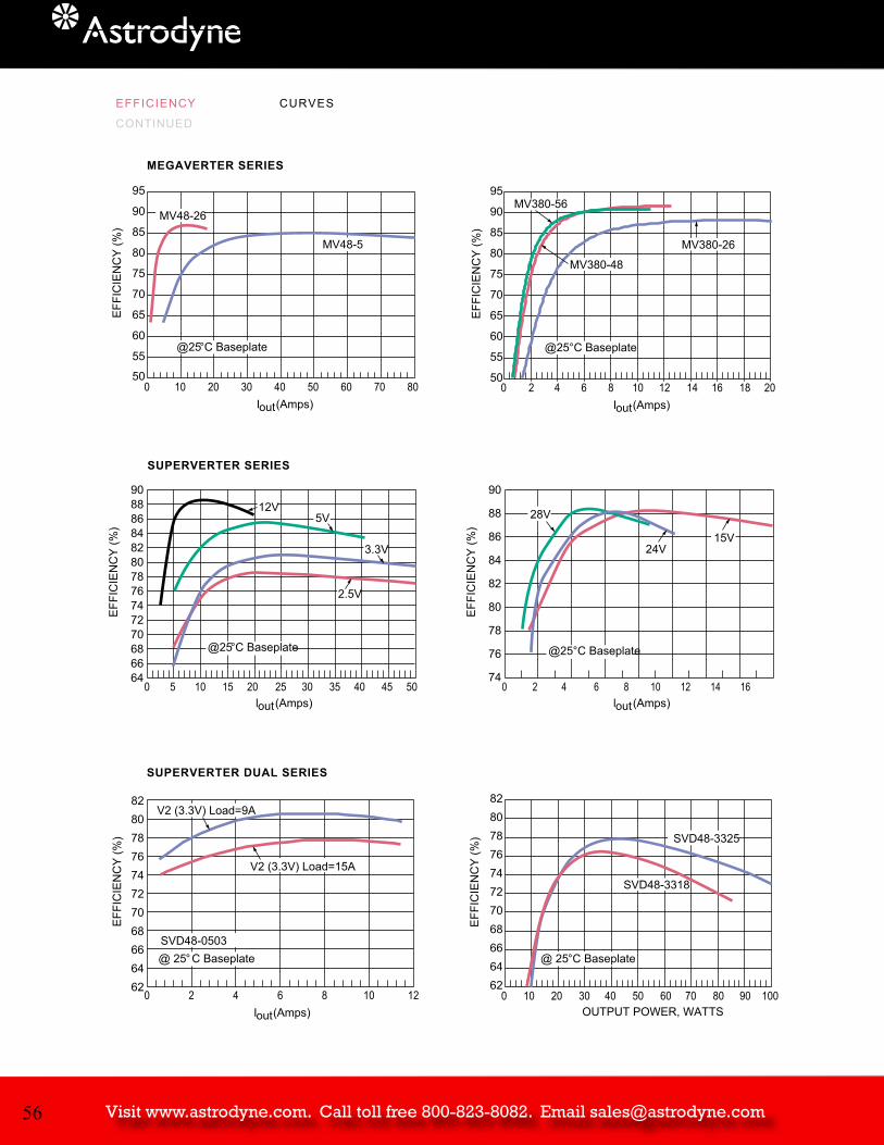
Visit www.astrodyne.com. Call toll free 800-823-8082. Email [email protected]
78
EFFICIENCY CURVES
CONTINUED
SUPERVERTER DUAL SERIES
EFF
ICIE
NC
Y (%
)
OUTPUT POWER, WATTS0 10 20 30 40 50 60 70 80 90 100
6264666870727476788082
SVD48-3318
SVD48-3325
@ 25°C Baseplate
EFF
ICIE
NC
Y (%
)
Iout (Amps)0 2 4 6 8 10 12
6264666870727476788082
V2 (3.3V) Load=15A
V2 (3.3V) Load=9A
@ 25°C BaseplateSVD48-0503
MEGAVERTER SERIES
Iout (Amps)0 10 20 30 40 50 60 70 80
EFF
ICIE
NC
Y (%
)
50
55
60
65
70
75
80
85
90
95
MV48-26
MV48-5
@25°C Baseplate
Iout (Amps)0 2 4 6 8 10 12 14 16 18 20
EFF
ICIE
NC
Y (%
)
50
55
60
65
70
75
80
85
90
95MV380-56
MV380-48
MV380-26
@25°C Baseplate
SUPERVERTER SERIES
9088868482807876747270686664
0 5 10 15 20 25 30 35 40 45 50
EFF
ICIE
NC
Y (%
)
lout (Amps)
@25°C Baseplate
2.5V
3.3V
5V12V
90
88
86
84
82
80
78
76
740 2 4 6 8 10 12 14 16
EFF
ICIE
NC
Y (%
)
lout (Amps)
24V
28V
15V
@25°C Baseplate

Visit www.astrodyne.com. Call toll free 800-823-8082. Email [email protected] 57
78
EFFICIENCY CURVES
CONTINUED
SUPERVERTER DUAL SERIES
EFF
ICIE
NC
Y (%
)
OUTPUT POWER, WATTS0 10 20 30 40 50 60 70 80 90 100
6264666870727476788082
SVD48-3318
SVD48-3325
@ 25°C Baseplate
EFF
ICIE
NC
Y (%
)
Iout (Amps)0 2 4 6 8 10 12
6264666870727476788082
V2 (3.3V) Load=15A
V2 (3.3V) Load=9A
@ 25°C BaseplateSVD48-0503
MEGAVERTER SERIES
Iout (Amps)0 10 20 30 40 50 60 70 80
EFF
ICIE
NC
Y (%
)
50
55
60
65
70
75
80
85
90
95
MV48-26
MV48-5
@25°C Baseplate
Iout (Amps)0 2 4 6 8 10 12 14 16 18 20
EFF
ICIE
NC
Y (%
)
50
55
60
65
70
75
80
85
90
95MV380-56
MV380-48
MV380-26
@25°C Baseplate
SUPERVERTER SERIES
9088868482807876747270686664
0 5 10 15 20 25 30 35 40 45 50
EFF
ICIE
NC
Y (%
)
lout (Amps)
@25°C Baseplate
2.5V
3.3V
5V12V
90
88
86
84
82
80
78
76
740 2 4 6 8 10 12 14 16
EFF
ICIE
NC
Y (%
)
lout (Amps)
24V
28V
15V
@25°C Baseplate
RO Associates | Tel: 408.744.1450 | Fax: 408.744.1521 | email: [email protected]
79
EFF
ICIE
NC
Y %
95
93
91
89
87
85
95
93
91
89
87
850 120 240 360 480 600 0 200 400 600 800 1000
OUTPUT POWER, WATTS
120 VAC, 100°C
120 VAC, 25°C
220 VAC, 100°C
220 VAC, 25°C
Efficiency PFC – 600
EFF
ICIE
NC
Y %
OUTPUT POWER, WATTS
25°C Case
100°C Case
Efficiency PFC – 1000
sledoM tuptuO V42 dna 21sledoM tuptuO V5 dna 3,2
Vin = 220VAC
NANOVERTER SERIES
PICOVERTER SERIES
UNIVERTER SERIES
85
80
75
70
65
600 25 50 75 100
EFF
ICIE
NC
Y (%
)
OUTPUT POWER, WATTS
Nominal Line, 25°C Case
nV 48-5
nV 48-2
nV 48-3
EFF
ICIE
NC
Y (%
)
90
85
80
75
700 25 50 75 100 125
OUTPUT POWER, WATTS
nV 48-24
nV 48-12
Nominal Line, 25°C Case
90
85
80
75
70
65
600 10 20 30 40 50 60
EFF
ICIE
NC
Y (%
)Efficiency – 12 and 24V Models
pV 48-12
pV 48-24
85
80
75
70
650 10 20 30 40 50
EFF
ICIE
NC
Y (%
)
OUTPUT POWER, WATTS
Efficiency – 3 and 5V Models
pV 48-3
pV 48-5
OUTPUT POWER, WATTS
Nominal Line, 25°C CaseNominal Line, 25°C Case

Visit www.astrodyne.com. Call toll free 800-823-8082. Email [email protected] 80
EFFICIENCY CURVES CONTINUED
OUTPUT POWER, WATTSAux. Loads Fixed at ±2A, 5V Load Varied
All Loads Varied
EFF
ICIE
NC
Y (%
)
85
80
75
7050 100 150 200
OUTPUT POWER, WATTS
90
85
80
7550 100 150 200 250
EFF
ICIE
NC
Y (%
)OUTPUT POWER, WATTS
EFF
ICIE
NC
Y (%
)
85
80
75
70
2.0
1.5
1.0
0.5
0.0
2.0
1.5
1.0
0.5
0.0
50 100 150 200 OUTPUT POWER, WATTS
5V Load Fixed, Aux. Output Loads Varied From 0 to 3A Each
5V@ 22A
5V@ 13A
5V@5A
85
80
75
7050 100 150 200
EFF
ICIE
NC
Y (%
)
5V
3.3V
2V
12V
24V
Triple Output Models
sledoM tuptuO V42 dna 21sledoM tuptuO V5 dna 3 ,2
Triple Output Models
30 36 42 48 54 60 66 72 78 84 9030 36 42 48 54 60 66 72 78 84 90
Minimum 5V Load vs. Auxiliary Output PowerµV28 and UV48-Triple Output Models
AUXILIARY OUTPUT POWER, WATTS
Tc=100°C
Tc=70°C
Minimum 5V Load vs. Auxiliary Output PowerUV300 Triple Output Models
AUXILIARY OUTPUT POWER, WATTS
Tc=100°C
Tc=25°C
5V L
OA
D (A
)
5V L
OA
D (A
)
MICROVERTER SERIES
MINIMUM LOAD –TRIPLES
Note: Efficiencies are typical for Tc=25°C and Nominal Input. Input and Output Voltages are measured at the Pins.

Visit www.astrodyne.com. Call toll free 800-823-8082. Email [email protected] 5980
EFFICIENCY CURVES CONTINUED
OUTPUT POWER, WATTSAux. Loads Fixed at ±2A, 5V Load Varied
All Loads Varied
EFF
ICIE
NC
Y (%
)
85
80
75
7050 100 150 200
OUTPUT POWER, WATTS
90
85
80
7550 100 150 200 250
EFF
ICIE
NC
Y (%
)
OUTPUT POWER, WATTS
EFF
ICIE
NC
Y (%
)
85
80
75
70
2.0
1.5
1.0
0.5
0.0
2.0
1.5
1.0
0.5
0.0
50 100 150 200 OUTPUT POWER, WATTS
5V Load Fixed, Aux. Output Loads Varied From 0 to 3A Each
5V@ 22A
5V@ 13A
5V@5A
85
80
75
7050 100 150 200
EFF
ICIE
NC
Y (%
)
5V
3.3V
2V
12V
24V
Triple Output Models
sledoM tuptuO V42 dna 21sledoM tuptuO V5 dna 3 ,2
Triple Output Models
30 36 42 48 54 60 66 72 78 84 9030 36 42 48 54 60 66 72 78 84 90
Minimum 5V Load vs. Auxiliary Output PowerµV28 and UV48-Triple Output Models
AUXILIARY OUTPUT POWER, WATTS
Tc=100°C
Tc=70°C
Minimum 5V Load vs. Auxiliary Output PowerUV300 Triple Output Models
AUXILIARY OUTPUT POWER, WATTS
Tc=100°C
Tc=25°C
5V L
OA
D (A
)
5V L
OA
D (A
)
MICROVERTER SERIES
MINIMUM LOAD –TRIPLES
Note: Efficiencies are typical for Tc=25°C and Nominal Input. Input and Output Voltages are measured at the Pins.
RO Associates | Tel: 408.744.1450 | Fax: 408.744.1521 | email: [email protected]
81
Included here are answers to some of the questions that our customers askmost frequently.
Q: What is the PWB footprint for the RO modules?
A: RO’s modules are generally smaller than our competition’s modules. The basic, recommended PWB footprints for our modules are shown in Application Note 19,Hole Dimensions and Socket Information.In addition, the outline drawings included in the product data sheets are another goodsource of information for creating customPWB footprints.
Q: How much heatsinking do I need for theRO converters?
A: The amount of heatsinking required is determined by the environment that themodule is placed in, the heat produced inthe module, and the maximum desiredbaseplate temperature. Because RO’s modules are highly efficient the requiredheatsinking is minimal. It may even be possible to operate the modules withoutany additional heatsinking. The thermal performance curves in this catalog weredesigned so that you can quickly determinethe amount of heatsinking required for yourapplication. A more in-depth discussion ofthermal design with the RO modules isavailable in Application Note 10, ThermalConsiderations.
Q: Why is a 1W, 6.2V Zener diode recommended on the Parallel Pin?
A: The Zener diode is recommended for any application that can see more than 6V, induced or applied, on the Parallel Pin.Accidental shorting of the Parallel Pin to a voltage greater than 6V will cause themodule to fail. A 1W, 6.2V Zener diode willprotect against most incidental shorts thatoccur during module testing as well as most externally induced transients thatoccur during operation.
Q: Why do I see 1V spikes on the output of the module?
A: These spikes do not really occur on the output, rather they are mostly the result ofnoise pickup and measurement error in thetest setup used. A common source of noisepickup is the loop created by the ground clip on most standard scope probes.Application Note 8, Noise and RippleMeasurement, discusses how to properlymeasure the output noise and ripple.
Q: Can RO modules be used with no additional components?
A: Yes, in some applications they can. However,bypass capacitors are often required toreduce system noise and achieve propermodule performance. For basic systems, we recommend that pads and traces for thecomponents shown in Figure 1 be includedin the initial PWB layout. The design teamcan then either optimize them for perform-ance or, if performance is good, eliminatethem for cost reduction.
Figure 1
Q: Paralleling De-coupling Modules (PDMs) are great when redundancy is required, but can the RO modules be paralleled without PDMs?
A: Yes, RO modules can be paralleled withoutany external components other than bypassand storage capacitors when redundancy isnot required. An exception to this, however,is the 300V MICROVERTER series; whichrequires a disconnect circuit to ensure anorderly startup. See Application Note 11 formore information.
FREQUENTLY ASKED QUESTIONS
+IN
+SENSE
-SENSE
TRIM
+OUT
-OUT-IN
PAR
MICROVERTERMODULE

Visit www.astrodyne.com. Call toll free 800-823-8082. Email [email protected] 82
Q: What is the recommended solder processfor the modules?
A: The recommended solder process is a wave solder process with the solder waveat 260°C. Each pin should be in the wave for5 seconds and the big pins should enter thewave last. Because the modules have a highthermal mass, the preheat cycle must belengthened in order for proper solder wetting of the pins to occur.
Q: Why do the modules sometimes seem tocurrent limit to early?
A: Noise on the Parallel Pin, the Input Pins, or the Output Pins can cause premature current limit in the modules. ApplicationNote 13 Paralleling- Current Sharing, Hot Plug-in, and N+M Redundancy andApplication Note 18 Board LayoutConsiderations and Recommendations provide some preventative and correctivemeasures that can be taken to reduce thenoise. Adding the proper bypass caps tothese pins will usually solve the problem.
Q: Why does the output noise increase when I connect the output return lines of thetriple output module together?
A: As with most multiple output power supplies,common mode noise can be injected fromone output into another causing increasednoise. Adding a small, common mode chokeof about 25µH per leg to each auxiliary out-put, before the common ground connection,will prevent this from occurring. SeeApplication Note 14 for more information.
Q: How does the output good signal function?
A: The output good signal provides an activelow output whenever the sensed outputvoltage is within ±10% of the set outputvoltage;otherwise it appears as an open collector (Vmax = 40V). The signal is referenced to -SENSE (See Figure 2) and
3.9K
3.9K
2N2222+
LOGICSIGNAL
-
PARALLELON/OFF
-IN
+SENSE
10%SENSINGCIRCUIT
-SENSE
OUTPUT GOOD
TRIM
is capable of sinking 15mA typical (8mAminimum). The output low voltage (saturation voltage) is 0.5V or less @ lsink = 1.6mA. The output good signalchanges its state in the range Vsense =±9% to ±11% of Vsetpoint.
Figure 2: Equivalent circuit of the Output Good Signal
Q: How do I use the ON/OFF pin?A: The ON/OFF pin may be used to turn the
module off and on remotely using a low level signal. When ON/OFF is pulled low (<1V @4mA, referenced to -Vin), the module is turned off. All that is required to interface the ON/OFF signal to the other circuits is a few external components as shown in Figure 3. Additional ways to use the ON/OFF pin are shown in Application Note 4, Logic On-Off.
Figure 3: Logic on/off circuit with small signal transistor. A logic high signal disables the converter.
FREQUENTLY ASKED QUESTIONSCONTINUED

Visit www.astrodyne.com. Call toll free 800-823-8082. Email [email protected] 6182
Q: What is the recommended solder processfor the modules?
A: The recommended solder process is a wave solder process with the solder waveat 260°C. Each pin should be in the wave for5 seconds and the big pins should enter thewave last. Because the modules have a highthermal mass, the preheat cycle must belengthened in order for proper solder wetting of the pins to occur.
Q: Why do the modules sometimes seem tocurrent limit to early?
A: Noise on the Parallel Pin, the Input Pins, or the Output Pins can cause premature current limit in the modules. ApplicationNote 13 Paralleling- Current Sharing, Hot Plug-in, and N+M Redundancy andApplication Note 18 Board LayoutConsiderations and Recommendations provide some preventative and correctivemeasures that can be taken to reduce thenoise. Adding the proper bypass caps tothese pins will usually solve the problem.
Q: Why does the output noise increase when I connect the output return lines of thetriple output module together?
A: As with most multiple output power supplies,common mode noise can be injected fromone output into another causing increasednoise. Adding a small, common mode chokeof about 25µH per leg to each auxiliary out-put, before the common ground connection,will prevent this from occurring. SeeApplication Note 14 for more information.
Q: How does the output good signal function?
A: The output good signal provides an activelow output whenever the sensed outputvoltage is within ±10% of the set outputvoltage;otherwise it appears as an open collector (Vmax = 40V). The signal is referenced to -SENSE (See Figure 2) and
3.9K
3.9K
2N2222+
LOGICSIGNAL
-
PARALLELON/OFF
-IN
+SENSE
10%SENSINGCIRCUIT
-SENSE
OUTPUT GOOD
TRIM
is capable of sinking 15mA typical (8mAminimum). The output low voltage (saturation voltage) is 0.5V or less @ lsink = 1.6mA. The output good signalchanges its state in the range Vsense =±9% to ±11% of Vsetpoint.
Figure 2: Equivalent circuit of the Output Good Signal
Q: How do I use the ON/OFF pin?A: The ON/OFF pin may be used to turn the
module off and on remotely using a low level signal. When ON/OFF is pulled low (<1V @4mA, referenced to -Vin), the module is turned off. All that is required to interface the ON/OFF signal to the other circuits is a few external components as shown in Figure 3. Additional ways to use the ON/OFF pin are shown in Application Note 4, Logic On-Off.
Figure 3: Logic on/off circuit with small signal transistor. A logic high signal disables the converter.
FREQUENTLY ASKED QUESTIONSCONTINUED
RO Associates | Tel: 408.744.1450 | Fax: 408.744.1521 | email: [email protected]
83
Apparent Power: The product of RMS voltage and RMS current.
Brownout: A drop or sag of the input voltagebelow a converter’s rated input range.
Current Limit: The point where the operationof a converter changes from constant voltagemode to constant current mode.
Current Sharing: Equal division of the totalload current between two or more modules.
Efficiency: The ratio of output power dividedby input power, expressed as a percentage.
Fault Tolerance: The capability of a power supply system to sustain one or more faultswithout degrading the power to the load.
Input Over Voltage: An increase or surge of the input voltage above a converter’s ratedinput range.
Input Reflected Ripple: The AC component ofthe input current of a converter resulting fromthe converter’s operation (high frequencyswitching), expressed as a percentage of theDC component.
Input Ripple Rejection: The attenuation of AC ripple a converter provides from its input to its output, expressed in dB.
Inrush Charge: The amount of charge, inCoulombs, that will flow into a converter uponapplication of nominal input voltage.
Isolation Voltage: The voltage that can beapplied between related circuits of a devicewithout voltage break down occurring in theinsulation between them.
Line Regulation: The change in a converter’soutput voltage resulting from a predefinedchange in the input voltage, expressed as apercentage of the output voltage.
Load Regulation: The change in a converter’soutput voltage resulting from a predefined
change in the load current, expressed as a percentage of the output voltage.
Minimum Load: The minimum load currentrequired for a converter to operate within specification.
Non-Shutdown Over Voltage Protection: The feature of a converter to continue supplying voltage to a load at a prescribedupper limit without shutting down and withoutrequiring reset when the event causing theover voltage condition is over.
Output Current Rating: The maximum current at which a converter will operate reliably and within its specifications.
Power Factor: The ratio of true input power toapparent input power in an AC input system.
Redundancy: The connection of multiple converters to provide uninterrupted power tothe load in the event of a converter failure.
Remote Sense Compensation: The amount ofvoltage drop that a converter can compensatefor between the output of the converter andthe sense point on the load.
Short-Circuit Current: The maximum outputcurrent that a converter will source with its output shorted, expressed as a percentage ofthe rated current.
Thermal Protection: The feature of a converterto protect itself, usually by shutting down,when its internal temperature reaches a prescribed maximum safe level.
Transient Response: The response of a converter’s output voltage to a defined, abruptchange in either the output current or the inputvoltage.
Turn-on Time: The time a converter takes to begin operating within specification afterproper power has been applied.
GLOSSARY
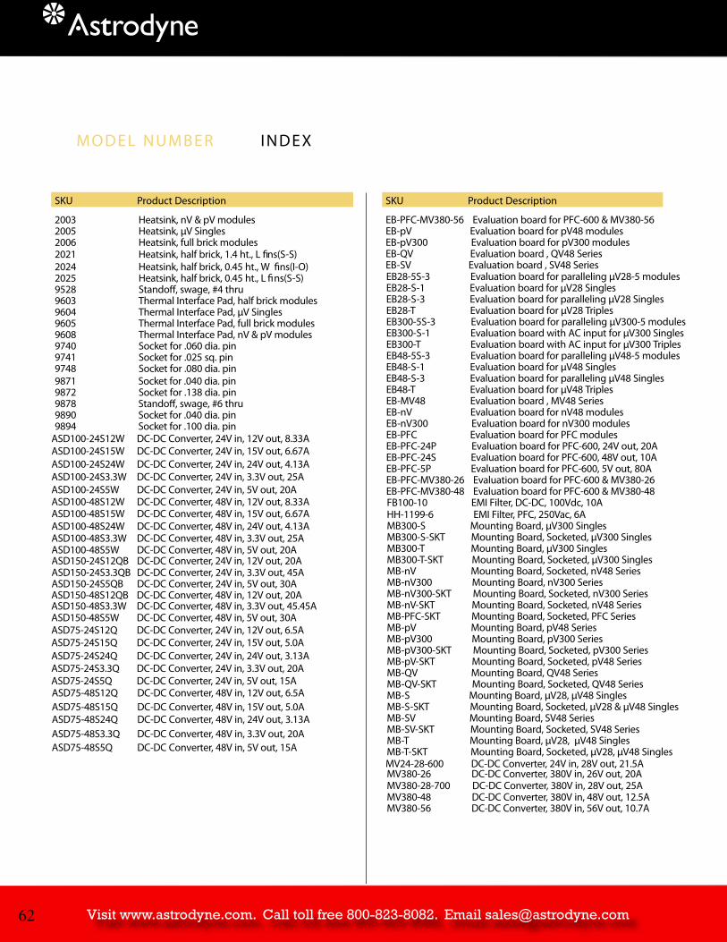
Visit www.astrodyne.com. Call toll free 800-823-8082. Email [email protected]
MODEL NUMBER INDEX
2003 Heatsink, nV & pV modules2005 Heatsink, µV Singles2006 Heatsink, full brick modules2021 Heatsink, half brick, 1.4 ht., L fins(S-S)2024 Heatsink, half brick, 0.45 ht., W fins(I-O)2025 Heatsink, half brick, 0.45 ht., L fins(S-S)9528 Stando, swage, #4 thru9603 Thermal Interface Pad, half brick modules9604 Thermal Interface Pad, µV Singles9605 Thermal Interface Pad, full brick modules9608 Thermal Interface Pad, nV & pV modules9740 Socket for .060 dia. pin9741 Socket for .025 sq. pin9748 Socket for .080 dia. pin9871 Socket for .040 dia. pin9872 Socket for .138 dia. pin9878 Stando, swage, #6 thru9890 Socket for .040 dia. pin9894 Socket for .100 dia. pin
EB28-5S-3 Evaluation board for paralleling µV28-5 modulesEB28-S-1 Evaluation board for µV28 SinglesEB28-S-3 Evaluation board for paralleling µV28 SinglesEB28-T Evaluation board for µV28 TriplesEB300-5S-3 Evaluation board for paralleling µV300-5 modulesEB300-S-1 Evaluation board with AC input for µV300 SinglesEB300-T Evaluation board with AC input for µV300 TriplesEB48-5S-3 Evaluation board for paralleling µV48-5 modulesEB48-S-1 Evaluation board for µV48 SinglesEB48-S-3 Evaluation board for paralleling µV48 SinglesEB48-T Evaluation board for µV48 TriplesEB-MV48 Evaluation board , MV48 SeriesEB-nV Evaluation board for nV48 modulesEB-nV300 Evaluation board for nV300 modulesEB-PFC Evaluation board for PFC modulesEB-PFC-24P Evaluation board for PFC-600, 24V out, 20AEB-PFC-24S Evaluation board for PFC-600, 48V out, 10AEB-PFC-5P Evaluation board for PFC-600, 5V out, 80AEB-PFC-MV380-26 Evaluation board for PFC-600 & MV380-26EB-PFC-MV380-48 Evaluation board for PFC-600 & MV380-48
EB-PFC-MV380-56 Evaluation board for PFC-600 & MV380-56EB-pV Evaluation board for pV48 modulesEB-pV300 Evaluation board for pV300 modulesEB-QV Evaluation board , QV48 SeriesEB-SV Evaluation board , SV48 Series
SKU Product Description SKU Product Description
ASD75-24S3.3Q DC-DC Converter, 24V in, 3.3V out, 20AASD75-24S5Q DC-DC Converter, 24V in, 5V out, 15A
ASD75-24S12Q DC-DC Converter, 24V in, 12V out, 6.5AASD75-24S15Q DC-DC Converter, 24V in, 15V out, 5.0AASD75-24S24Q DC-DC Converter, 24V in, 24V out, 3.13A
ASD75-48S3.3Q DC-DC Converter, 48V in, 3.3V out, 20AASD75-48S5Q DC-DC Converter, 48V in, 5V out, 15A
ASD75-48S12Q DC-DC Converter, 48V in, 12V out, 6.5AASD75-48S15Q DC-DC Converter, 48V in, 15V out, 5.0AASD75-48S24Q DC-DC Converter, 48V in, 24V out, 3.13A
ASD100-24S3.3W DC-DC Converter, 24V in, 3.3V out, 25AASD100-24S5W DC-DC Converter, 24V in, 5V out, 20A
ASD100-24S12W DC-DC Converter, 24V in, 12V out, 8.33AASD100-24S15W DC-DC Converter, 24V in, 15V out, 6.67AASD100-24S24W DC-DC Converter, 24V in, 24V out, 4.13A
ASD100-48S3.3W DC-DC Converter, 48V in, 3.3V out, 25AASD100-48S5W DC-DC Converter, 48V in, 5V out, 20A
ASD100-48S12W DC-DC Converter, 48V in, 12V out, 8.33AASD100-48S15W DC-DC Converter, 48V in, 15V out, 6.67AASD100-48S24W DC-DC Converter, 48V in, 24V out, 4.13A
ASD150-24S3.3QB DC-DC Converter, 24V in, 3.3V out, 45AASD150-24S5QB DC-DC Converter, 24V in, 5V out, 30A
ASD150-24S12QB DC-DC Converter, 24V in, 12V out, 20A
ASD150-48S3.3W DC-DC Converter, 48V in, 3.3V out, 45.45AASD150-48S5W DC-DC Converter, 48V in, 5V out, 30A
ASD150-48S12QB DC-DC Converter, 48V in, 12V out, 20A
FB100-10 EMI Filter, DC-DC, 100Vdc, 10AHH-1199-6 EMI Filter, PFC, 250Vac, 6AMB300-S Mounting Board, µV300 SinglesMB300-S-SKT Mounting Board, Socketed, µV300 SinglesMB300-T Mounting Board, µV300 SinglesMB300-T-SKT Mounting Board, Socketed, µV300 SinglesMB-nV Mounting Board, Socketed, nV48 SeriesMB-nV300 Mounting Board, nV300 SeriesMB-nV300-SKT Mounting Board, Socketed, nV300 SeriesMB-nV-SKT Mounting Board, Socketed, nV48 SeriesMB-PFC-SKT Mounting Board, Socketed, PFC SeriesMB-pV Mounting Board, pV48 SeriesMB-pV300 Mounting Board, pV300 SeriesMB-pV300-SKT Mounting Board, Socketed, pV300 SeriesMB-pV-SKT Mounting Board, Socketed, pV48 SeriesMB-QV Mounting Board, QV48 SeriesMB-QV-SKT Mounting Board, Socketed, QV48 SeriesMB-S Mounting Board, µV28, µV48 SinglesMB-S-SKT Mounting Board, Socketed, µV28 & µV48 SinglesMB-SV Mounting Board, SV48 SeriesMB-SV-SKT Mounting Board, Socketed, SV48 SeriesMB-T Mounting Board, µV28, µV48 SinglesMB-T-SKT Mounting Board, Socketed, µV28, µV48 Singles
MV380-26 DC-DC Converter, 380V in, 26V out, 20A
MV380-48 DC-DC Converter, 380V in, 48V out, 12.5AMV380-56 DC-DC Converter, 380V in, 56V out, 10.7A
MV24-28-600 DC-DC Converter, 24V in, 28V out, 21.5A
MV380-28-700 DC-DC Converter, 380V in, 28V out, 25A
RO Associates | Tel: 408.744.1450 | Fax: 408.744.1521 | email: [email protected]
85
uV28-12 DC-DC Converter, 28V in, 12V out, 20AuV28-15 DC-DC Converter, 28V in, 15V out, 16AuV28-2 DC-DC Converter, 28V in, 2.1V out, 60AuV28-24 DC-DC Converter, 28V in, 24V out, 10AuV28-28 DC-DC Converter, 28V in, 28V out, 9AuV28-3 DC-DC Converter, 28V in, 3.3V out, 50AuV28-5 DC-DC Converter, 28V in, 5V out, 40AuV28-8 DC-DC Converter, 28V in, 8V out, 30AuV28-T512 DC-DC Converter, 28V in, 5V, ±12V, 185WuV28-T515 DC-DC Converter, 28V in, 5V, ±15V, 185WuV300-12 DC-DC Converter, 300V in, 12V out, 20AuV300-15 DC-DC Converter, 300V in, 15V out, 16AuV300-2 DC-DC Converter, 300V in, 2.1V out, 60AuV300-24 DC-DC Converter, 300V in, 24V out, 10AuV300-28 DC-DC Converter, 300V in, 28V out, 9AuV300-3 DC-DC Converter, 300V in, 3.3V out, 50AuV300-5 DC-DC Converter, 300V in, 5V out, 40A
uV300-8 DC-DC Converter, 300V in, 8V out, 30A
uV300-T512 DC-DC Converter, 300V in, 5V, ±12V, 185WuV300-T515 DC-DC Converter, 300V in, 5V, ±15V, 185WuV48-12 DC-DC Converter, 48V in, 12V out, 20AuV48-15 DC-DC Converter, 48V in, 15V out, 16AuV48-2 DC-DC Converter, 48V in, 2.1V out, 60AuV48-24 DC-DC Converter, 48V in, 24V out, 10AuV48-28 DC-DC Converter, 48V in, 28V out, 9AuV48-3 DC-DC Converter, 48V in, 3.3V out, 50AuV48-5 DC-DC Converter, 48V in, 5V out, 40A
uV48-8 DC-DC Converter, 48V in, 8V out, 30A
uV48-T512 DC-DC Converter, 48V in, 5V, ±12V, 185WuV48-T515 DC-DC Converter, 48V in, 5V, ±15V, 185W
SKU Product Description SKU Product Description
uV24-5-164 DC-DC Converter, 24V in, 5V out, 20AnV300-12 DC-DC Converter, 300V in, 12V out, 10AnV300-15 DC-DC Converter, 300V in, 15V out, 8AnV300-2 DC-DC Converter, 300V in, 2.1V out, 30AnV300-24 DC-DC Converter, 300V in, 24V out, 5AnV300-3 DC-DC Converter, 300V in, 3.3V out, 25AnV300-5 DC-DC Converter, 300V in, 5V out, 20APDM Parallel Decoupling ModulePFC-1000 AC-DC Converter, PFC, 1000W, European InputPFC-600 AC-DC Converter, PFC, 600W, Universal Input
pV300-12 DC-DC Converter, 300V in, 12V out, 5ApV300-15 DC-DC Converter, 300V in, 15V out, 4ApV300-24 DC-DC Converter, 300V in, 24V out, 2.5ApV300-3 DC-DC Converter, 300V in, 3.3V out, 12.5ApV300-5 DC-DC Converter, 300V in, 5V out, 10A
SV28-12-150-1 DC-DC Converter, 28V in, 12V out, 12.5ASV28-2.5-150-1 DC-DC Converter, 28V in, 2.5V out, 30ASV28-24-150-1 DC-DC Converter, 28V in, 24V out, 12.5ASV28-28-150-1 DC-DC Converter, 28V in, 28V out, 5.35ASV28-3-150-1 DC-DC Converter, 28V in, 3.3V out, 30ASV28-3-150-1 DC-DC Converter, 28V in, 3.3V out, 30ASV28-3-200-1 DC-DC Converter, 28V in, 3.3V out, 40ASV28-5-150-1 DC-DC Converter, 28V in, 5V out, 30ASV28-5-175-1 DC-DC Converter, 28V in, 5V out, 35ASV28-5-175-14 DC-DC Converter, 28V in, 5V out, 35A,
Thru HoleSV48-12-150-1 DC-DC Converter, 48V in, 12V out, 12.5ASV48-12-200-1 DC-DC Converter, 48V in, 12V out, 20ASV48-15-150-1 DC-DC Converter, 48V in, 15V out, 10ASV48-15-200-1 DC-DC Converter, 48V in, 15V out, 16ASV48-2.5-150-1 DC-DC Converter, 48V in, 2.5V out, 30ASV48-2.5-200-1 DC-DC Converter, 48V in, 2.5V out, 50ASV48-24-200-1 DC-DC Converter, 48V in, 24V out, 10ASV48-28-150-1 DC-DC Converter, 48V in, 28V out, 5.35ASV48-28-200-1 DC-DC Converter, 48V in, 28V out, 8.6ASV48-3-150-1 DC-DC Converter, 48V in, 3.3V out, 30ASV48-3-200-1 DC-DC Converter, 48V in, 3.3V out, 45ASV48-5-150-1 DC-DC Converter, 48V in, 5V out, 30ASV48-5-200-1 DC-DC Converter, 48V in, 5V out, 40A
PFC-650 AC-DC Converter, PFC, 650W, Universal Input
uV24-8-164 DC-DC Converter, 24V in, 8V out, 36AuV24-12-164 DC-DC Converter, 24V in, 12V out, 25AuV24-15-164 DC-DC Converter, 24V in, 15V out, 20AuV24-24-164 DC-DC Converter, 24V in, 24V out, 12.5AuV24-28-164 DC-DC Converter, 24V in, 28V out, 11A
uV48-5-164 DC-DC Converter, 48V in, 5V out, 20A
uV48-12-164 DC-DC Converter, 48V in, 12V out, 25AuV48-15-164 DC-DC Converter, 48V in, 15V out, 20A
uV300-5-164 DC-DC Converter, 300V in, 5V out, 20W
uV300-8-164 DC-DC Converter, 300V in, 8V out, 36AuV300-12-164 DC-DC Converter, 300V in, 12V out, 25AuV300-15-164 DC-DC Converter, 300V in, 15V out, 20AuV300-24-164 DC-DC Converter, 300V in, 24V out, 12.5AuV300-28-164 DC-DC Converter, 300V in, 28V out, 11A
SMV-28-500 DC-DC Converter, 300V in, 28V out, 18A

Visit www.astrodyne.com. Call toll free 800-823-8082. Email [email protected] 63
RO Associates | Tel: 408.744.1450 | Fax: 408.744.1521 | email: [email protected]
85
uV28-12 DC-DC Converter, 28V in, 12V out, 20AuV28-15 DC-DC Converter, 28V in, 15V out, 16AuV28-2 DC-DC Converter, 28V in, 2.1V out, 60AuV28-24 DC-DC Converter, 28V in, 24V out, 10AuV28-28 DC-DC Converter, 28V in, 28V out, 9AuV28-3 DC-DC Converter, 28V in, 3.3V out, 50AuV28-5 DC-DC Converter, 28V in, 5V out, 40AuV28-8 DC-DC Converter, 28V in, 8V out, 30AuV28-T512 DC-DC Converter, 28V in, 5V, ±12V, 185WuV28-T515 DC-DC Converter, 28V in, 5V, ±15V, 185WuV300-12 DC-DC Converter, 300V in, 12V out, 20AuV300-15 DC-DC Converter, 300V in, 15V out, 16AuV300-2 DC-DC Converter, 300V in, 2.1V out, 60AuV300-24 DC-DC Converter, 300V in, 24V out, 10AuV300-28 DC-DC Converter, 300V in, 28V out, 9AuV300-3 DC-DC Converter, 300V in, 3.3V out, 50AuV300-5 DC-DC Converter, 300V in, 5V out, 40A
uV300-8 DC-DC Converter, 300V in, 8V out, 30A
uV300-T512 DC-DC Converter, 300V in, 5V, ±12V, 185WuV300-T515 DC-DC Converter, 300V in, 5V, ±15V, 185WuV48-12 DC-DC Converter, 48V in, 12V out, 20AuV48-15 DC-DC Converter, 48V in, 15V out, 16AuV48-2 DC-DC Converter, 48V in, 2.1V out, 60AuV48-24 DC-DC Converter, 48V in, 24V out, 10AuV48-28 DC-DC Converter, 48V in, 28V out, 9AuV48-3 DC-DC Converter, 48V in, 3.3V out, 50AuV48-5 DC-DC Converter, 48V in, 5V out, 40A
uV48-8 DC-DC Converter, 48V in, 8V out, 30A
uV48-T512 DC-DC Converter, 48V in, 5V, ±12V, 185WuV48-T515 DC-DC Converter, 48V in, 5V, ±15V, 185W
SKU Product Description SKU Product Description
uV24-5-164 DC-DC Converter, 24V in, 5V out, 20AnV300-12 DC-DC Converter, 300V in, 12V out, 10AnV300-15 DC-DC Converter, 300V in, 15V out, 8AnV300-2 DC-DC Converter, 300V in, 2.1V out, 30AnV300-24 DC-DC Converter, 300V in, 24V out, 5AnV300-3 DC-DC Converter, 300V in, 3.3V out, 25AnV300-5 DC-DC Converter, 300V in, 5V out, 20APDM Parallel Decoupling ModulePFC-1000 AC-DC Converter, PFC, 1000W, European InputPFC-600 AC-DC Converter, PFC, 600W, Universal Input
pV300-12 DC-DC Converter, 300V in, 12V out, 5ApV300-15 DC-DC Converter, 300V in, 15V out, 4ApV300-24 DC-DC Converter, 300V in, 24V out, 2.5ApV300-3 DC-DC Converter, 300V in, 3.3V out, 12.5ApV300-5 DC-DC Converter, 300V in, 5V out, 10A
SV28-12-150-1 DC-DC Converter, 28V in, 12V out, 12.5ASV28-2.5-150-1 DC-DC Converter, 28V in, 2.5V out, 30ASV28-24-150-1 DC-DC Converter, 28V in, 24V out, 12.5ASV28-28-150-1 DC-DC Converter, 28V in, 28V out, 5.35ASV28-3-150-1 DC-DC Converter, 28V in, 3.3V out, 30ASV28-3-150-1 DC-DC Converter, 28V in, 3.3V out, 30ASV28-3-200-1 DC-DC Converter, 28V in, 3.3V out, 40ASV28-5-150-1 DC-DC Converter, 28V in, 5V out, 30ASV28-5-175-1 DC-DC Converter, 28V in, 5V out, 35ASV28-5-175-14 DC-DC Converter, 28V in, 5V out, 35A,
Thru HoleSV48-12-150-1 DC-DC Converter, 48V in, 12V out, 12.5ASV48-12-200-1 DC-DC Converter, 48V in, 12V out, 20ASV48-15-150-1 DC-DC Converter, 48V in, 15V out, 10ASV48-15-200-1 DC-DC Converter, 48V in, 15V out, 16ASV48-2.5-150-1 DC-DC Converter, 48V in, 2.5V out, 30ASV48-2.5-200-1 DC-DC Converter, 48V in, 2.5V out, 50ASV48-24-200-1 DC-DC Converter, 48V in, 24V out, 10ASV48-28-150-1 DC-DC Converter, 48V in, 28V out, 5.35ASV48-28-200-1 DC-DC Converter, 48V in, 28V out, 8.6ASV48-3-150-1 DC-DC Converter, 48V in, 3.3V out, 30ASV48-3-200-1 DC-DC Converter, 48V in, 3.3V out, 45ASV48-5-150-1 DC-DC Converter, 48V in, 5V out, 30ASV48-5-200-1 DC-DC Converter, 48V in, 5V out, 40A
PFC-650 AC-DC Converter, PFC, 650W, Universal Input
uV24-8-164 DC-DC Converter, 24V in, 8V out, 36AuV24-12-164 DC-DC Converter, 24V in, 12V out, 25AuV24-15-164 DC-DC Converter, 24V in, 15V out, 20AuV24-24-164 DC-DC Converter, 24V in, 24V out, 12.5AuV24-28-164 DC-DC Converter, 24V in, 28V out, 11A
uV48-5-164 DC-DC Converter, 48V in, 5V out, 20A
uV48-12-164 DC-DC Converter, 48V in, 12V out, 25AuV48-15-164 DC-DC Converter, 48V in, 15V out, 20A
uV300-5-164 DC-DC Converter, 300V in, 5V out, 20W
uV300-8-164 DC-DC Converter, 300V in, 8V out, 36AuV300-12-164 DC-DC Converter, 300V in, 12V out, 25AuV300-15-164 DC-DC Converter, 300V in, 15V out, 20AuV300-24-164 DC-DC Converter, 300V in, 24V out, 12.5AuV300-28-164 DC-DC Converter, 300V in, 28V out, 11A
SMV-28-500 DC-DC Converter, 300V in, 28V out, 18A

New DC/DC Converter Modules
www.astrodyne.com800-823-8082
New Product Series
ASD75Q Wide Input
ASD100W Wide Input
ASD150QB
UV-164 Generation II MicroVerter Series
PFC-650 Series
MV24-28-600
SMV-28-500

The Un ive r te r PFC-650 Power Fac to r Correction modules are AC to DC converters that operate from wide range AC input voltages and frequencies with extremely high conversion eff ic iency and near uni ty power factor, producing an output of 375VDC. The PFC-650U operates from the universal input voltage range of 90 to 265VAC and input frequencies in the range of 47 to 440Hz making it ideal for applications requiring Power Factor Correction the world over. Model PFC-650W is optimized for input voltages in the 90 to 180VAC range and input frequencies in the range of 330 to 880Hz making it an ideal choice for both military and commerc ia l a i r c ra f t app l i ca t ions . These compact power modules use advanced electrical design and thermal management techniques that make them suitable for rugged, environmentally challenged applications.
• Extremely High Efficiency – 94% typ • Near Unity Power Factor – 0.99 typ. • High Power Density – 150W/in³ • -40ºC to +100 ºC Operation Standard • -55ºC to +100 ºC Operation Optional • Extremely Low Thermal Resistance • Conduction Cooled
Rugged Encapsulated Package • Active Inrush Current Limiting • LD ENA Signal Controls Downstream
Converters • MIL-STD-704/DO-160 Compatible
MODEL InputVoltage, VAC
InputFrequency, Hz
PFC-650U 90 - 265 47 - 440
PFC-650W 90 - 180 330 - 880
PFC‐650 Series Univerter® Power Factor Correction Module
FEATURES
Compact ¾ Brick Package3.6 x 2.4 x 0.5 in.
MODEL SELECTION
Astrodyne USA: 1‐800‐823‐8082 Astrodyne Pacific: 886‐2‐26983458
Typical Application:
650 Watt PFC Front End
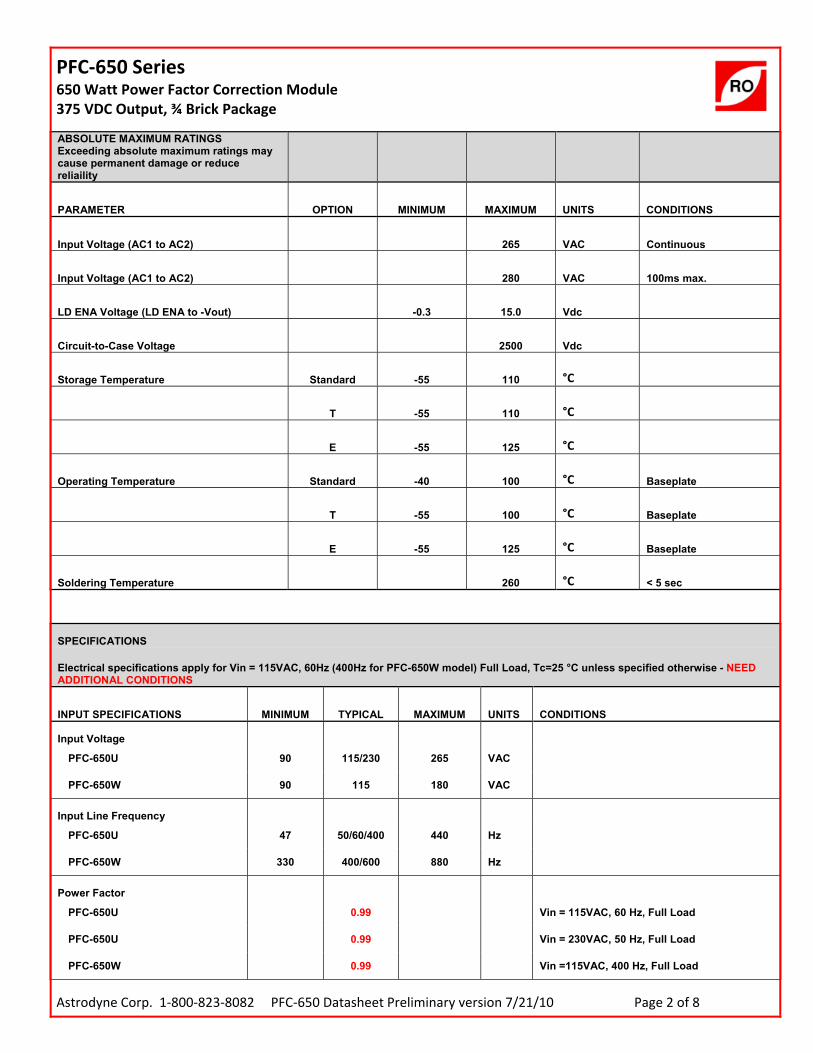
PFC‐650 Series 650 Watt Power Factor Correction Module 375 VDC Output, ¾ Brick Package
Astrodyne Corp. 1‐800‐823‐8082 PFC‐650 Datasheet Preliminary version 7/21/10 Page 2 of 8
ABSOLUTE MAXIMUM RATINGS Exceeding absolute maximum ratings may cause permanent damage or reduce reliaility
PARAMETER OPTION MINIMUM MAXIMUM UNITS CONDITIONS
Input Voltage (AC1 to AC2) 265 VAC Continuous
Input Voltage (AC1 to AC2) 280 VAC 100ms max.
LD ENA Voltage (LD ENA to -Vout) -0.3 15.0 Vdc
Circuit-to-Case Voltage 2500 Vdc
Storage Temperature Standard -55 110 °C
T -55 110 °C
E -55 125 °C
Operating Temperature Standard -40 100 °C Baseplate
T -55 100 °C Baseplate
E -55 125 °C Baseplate
Soldering Temperature 260 °C < 5 sec
SPECIFICATIONS
Electrical specifications apply for Vin = 115VAC, 60Hz (400Hz for PFC-650W model) Full Load, Tc=25 °C unless specified otherwise - NEEDADDITIONAL CONDITIONS
INPUT SPECIFICATIONS MINIMUM TYPICAL MAXIMUM UNITS CONDITIONS
Input Voltage
PFC-650U 90 115/230 265 VAC
PFC-650W 90 115 180 VAC
Input Line Frequency
PFC-650U 47 50/60/400 440 Hz
PFC-650W 330 400/600 880 Hz
Power Factor
PFC-650U 0.99 Vin = 115VAC, 60 Hz, Full Load
PFC-650U 0.99 Vin = 230VAC, 50 Hz, Full Load
PFC-650W 0.99 Vin =115VAC, 400 Hz, Full Load

PFC‐650 Series 650 Watt Power Factor Correction Module 375 VDC Output, ¾ Brick Package
Astrodyne Corp. 1‐800‐823‐8082 PFC‐650 Datasheet Preliminary version 7/21/10 Page 3 of 8
SPECIFICATIONS (continued)
Electrical specifications apply for Vin = 115VAC, 60Hz (400Hz for PFC-650W model) Full Load, Tc=25 °C unless specified otherwise - NEEDADDITIONAL CONDITIONS
Total Harmonic Distortion
PFC-650U TBD
PFC-650W TBD
Maximum Input Current 8.1 Arms Vin = 90VAC, Full Load, Tc = 25°C
6.2 Arms Vin = 115VAC, Tc = 100°C
Inrush Current
PFC-650U TBD TBD
PFC-650W 10 A NEED CONDITIONS
Input-to-Case Leakage Current TBD µArms Vin = 115VAC, Single Ø with one lead earthed
Start-up Voltage 70 80 85 VAC
Input Under Voltage 65 75 85 VAC
Ride Through Time 60 ms NEED CONDITIONS
OUTPUT SPECIFICATIONS MINIMUM TYPICAL MAXIMUM UNITS CONDITIONS
Output Voltage 370 375 380 Vdc Vin = 115VAC, Tc = 25°C
Output Current 0 1.75 ADC
Output Current Limit NONE
Ripple
PFC-650U TBD TBD V p-p Vin = 115VAC, f = 60Hz, C hold up =
PFC-650W TBD TBD V p-p Vin = 115VAC, f = 400Hz, C hold up =
Hold Up Capacitance
PFC-650U 220 1000 µF
PFC-650W 40 220 µF
Efficiency
PFC-650U 0.94 Vin = 115VAC, 60 Hz, Full Load
PFC-650U 0.96 Vin = 230VAC, 50 Hz, Full Load
PFC-650W 0.94 Vin =115VAC, 400 Hz, Full Load
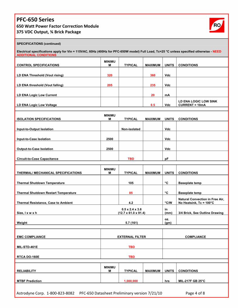
PFC‐650 Series 650 Watt Power Factor Correction Module 375 VDC Output, ¾ Brick Package
Astrodyne Corp. 1‐800‐823‐8082 PFC‐650 Datasheet Preliminary version 7/21/10 Page 4 of 8
SPECIFICATIONS (continued)
Electrical specifications apply for Vin = 115VAC, 60Hz (400Hz for PFC-650W model) Full Load, Tc=25 °C unless specified otherwise - NEEDADDITIONAL CONDITIONS
CONTROL SPECIFICATIONS MINIMU
M TYPICAL MAXIMUM UNITS CONDITIONS
LD ENA Threshold (Vout rising) 320 360 Vdc
LD ENA threshold (Vout falling) 205 235 Vdc
LD ENA Logic Low Current 20 mA
LD ENA Logic Low Voltage 0.5 Vdc LD ENA LOGIC LOW SINK CURRENT = 10mA
ISOLATION SPECIFICATIONS MINIMU
M TYPICAL MAXIMUM UNITS CONDITIONS
Input-to-Output Isolation Non-isolated Vdc
Input-to-Case Isolation 2500 Vdc
Output-to-Case Isolation 2500 Vdc
Circuit-to-Case Capacitance TBD pF
THERMAL/ MECHANICAL SPECIFICATIONS MINIMU
M TYPICAL MAXIMUM UNITS CONDITIONS
Thermal Shutdown Temperature 105 °C Baseplate temp
Thermal Shutdown Restart Temperature 85 °C Baseplate temp
Thermal Resistance, Case to Ambient 4.2 °C/W Natural Convection in Free Air, No Heatsink, Tc = 100°C
Size, l x w x h 0.5 x 2.4 x 3.6
(12.7 x 61.0 x 91.4) in(mm) 3/4 Brick, See Outline Drawing
Weight 5.7 (161) oz. (gm)
EMC COMPLIANCE EXTERNAL FILTER COMPLIANCE
MIL-STD-461E TBD
RTCA DO-160E TBD
RELIABILITY MINIMU
M TYPICAL MAXIMUM UNITS CONDITIONS
MTBF Prediction 1,000,000 hrs MIL-217F GB 25°C
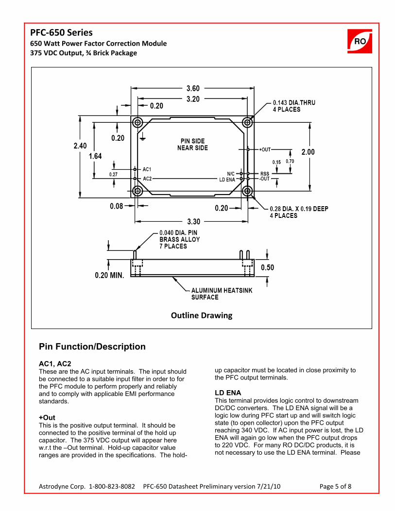
PFC‐650 Series 650 Watt Power Factor Correction Module 375 VDC Output, ¾ Brick Package
Astrodyne Corp. 1‐800‐823‐8082 PFC‐650 Datasheet Preliminary version 7/21/10 Page 5 of 8
Pin Function/Description
AC1, AC2 These are the AC input terminals. The input should be connected to a suitable input filter in order to for the PFC module to perform properly and reliably and to comply with applicable EMI performance standards.
+Out This is the positive output terminal. It should be connected to the positive terminal of the hold up capacitor. The 375 VDC output will appear here w.r.t the –Out terminal. Hold-up capacitor value ranges are provided in the specifications. The hold-
up capacitor must be located in close proximity to the PFC output terminals.
LD ENA This terminal provides logic control to downstream DC/DC converters. The LD ENA signal will be a logic low during PFC start up and will switch logic state (to open collector) upon the PFC output reaching 340 VDC. If AC input power is lost, the LD ENA will again go low when the PFC output drops to 220 VDC. For many RO DC/DC products, it is not necessary to use the LD ENA terminal. Please
Outline Drawing

PFC‐650 Series 650 Watt Power Factor Correction Module 375 VDC Output, ¾ Brick Package
Astrodyne Corp. 1‐800‐823‐8082 PFC‐650 Datasheet Preliminary version 7/21/10 Page 6 of 8
see the applications notes or consult the factory for more information.
RSS This terminal is internally connected to inrush control circuitry on model PFC-650U and is N/C on model PFC-650W. Model PFC-650W has a built in inrush limiting resistor whereas for model PFC-650U the resistor must be provided externally. For PFC-650U, connect one end of the inrush limiting resistor to this terminal. The other end of the resistor will be connected to –Out. The external inrush resistor
must be chosen to handle the inrush energy which is determined by the input voltage and hold-up capacitor value selected. The inrush connection diagram provides some specific recommendations. Consult the factory for assistance or additional information on selecting an inrush resistor.
-Out This is the PFC negative output terminal. It should be connected to the negative terminal of the hold up capacitor. For model PFC-650U, connect one end of the inrush resistor to this terminal.
Application Diagrams The connection diagrams below show proper connections between PFC-650 modules, hold-up capacitor, inrush limiting resistor (if required) and DC/DC converters.
For PFC-650W, the inrush limiting resistor is built-in and an external resistor is not required. The resistor is appropriately sized for a maximum input voltage of 180VAC and a maximum external hold-up capacitor value of TBD.
For PFC-650U, an external inrush limiting resistor must be provided and connected as shown in the connection diagram for PFC-650U. A resistor with high surge handling capability should be used. The maximum input voltage, external hold-up capacitor value and temperature must be considered in choosing a resistor. The maximum RMS input voltage and resistor value will determine the maximum inrush current. A resistor value of at least 10 ohms should be chosen. The surge energy in the resistor is that required to charge the hold-up capacitor up to the peak of the line. After that, internal circuitry will both bypass the external resistor with essentially a short circuit and limit additional inrush current to TBD Amps.
See also the Start-up and Shutdown Timing Diagram for additional information.
Connection Diagram for PFC‐650W

PFC‐650 Series 650 Watt Power Factor Correction Module 375 VDC Output, ¾ Brick Package
Astrodyne Corp. 1‐800‐823‐8082 PFC‐650 Datasheet Preliminary version 7/21/10 Page 8 of 8
80%
85%
90%
95%
100%
0 50 100 150 200 250 300 350 400 450 500 550
Pw
er
Fa
cto
r
Pout, Watts
PFC-650U 115VAC Input, 60Hz230VAC, 50Hz
PFC‐650U POWER FACTOR
80%
85%
90%
95%
100%
0 50 100 150 200 250 300 350 400 450 500 550
Eff
icie
nc
y, %
Pout, Watts
PFC-650U 115VAC Input, 60Hz230VAC, 50Hz
PFC‐650U EFFICIENCY
80%
85%
90%
95%
100%
0 50 100 150 200 250 300 350 400 450 500 550
Po
we
r L
oss
Pout, Watts
PFC-650U 115VAC Input, 60Hz230VAC, 50Hz
PFC‐650U POWER LOSS
80%
85%
90%
95%
100%
0 50 100 150 200 250 300 350 400 450 500 550
Pw
er
Fa
cto
r
Pout, Watts
PFC-650W 115VAC Input, 400Hz115VAC, 800Hz
PFC‐650U POWER FACTOR
80%
85%
90%
95%
100%
0 50 100 150 200 250 300 350 400 450 500 550
Eff
icie
nc
y, %
Pout, Watts
PFC-650U 115VAC Input, 400Hz115VAC, 800Hz
PFC‐650U EFFICIENCY
80%
85%
90%
95%
100%
0 50 100 150 200 250 300 350 400 450 500 550
Po
we
r L
oss
Pout, Watts
PFC-650U 115VAC Input, 400Hz115VAC, 800Hz
PFC‐650U POWER LOSS
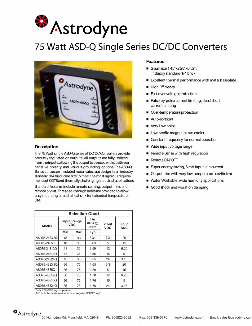
A
75 Watt ASD-Q Single Series DC/DC Converters
1
FeaturesSmall size 1.45”x2.28”x0.52”, industry standard 1/4 brick
Excellent thermal performance with metal baseplate
Fast over voltage protection
Pulse-by-pulse current limiting, dead shortcurrent limiting
Over-temperature protection
Auto-softstart
Very Low noise
Low magnetics run cooler
Constant frequency for normal operation
Wide input voltage range
Remote Sense with high regulation
Remote ON/OFF
Super energy saving, 6 mA input idle current
Output trim with very low temperature
Water Washable, wide humidity applications
Good shock and vibration damping
DescriptionThe 75 Watt single ASD-Q series of DC/DC Converters provideprecisely regulated dc outputs. All outputs are fully isolatedfrom the inputs, allowing the output to be used with positive ornegative polarity and various grounding options. The ASD-QSeries utilizes an insulated metal substrate design in an industry
Standard features include remote sensing, output trim, andremote Threaded-through holes are provided to alloweasy mounting or add a heat sink for extended temperatureuse.
trahCnoitceleS
ledoMegnaRtupnI
CDVniI
@CDAmon
tuoVCDV
tuoICDA
niM xaM pyT
ASD75-24S3.3Q 3.31 2036 36.3 5 51
81 63 95.3 21 52.681 63 55.3 51 581 63 55.3 42 31.363 57 56.1 3.3 0263 57 08.1 5 5163 57 87.1 21 52.663 57 67.1 51 563 57 67.1 42 31.3
.evitisopsicigolFFO/NOtluafeD.cigolFFO/NOevitagenredrootrebmunledomehtotN-ddA
18 36 3.3ASD75-24S5Q 18
ASD75-24S12QASD75-24S15QASD75-24S24QASD75-48S3.3QASD75-48S5Q
ASD75-48S12QASD75-48S15QASD75-48S24Q
35 Hampden Rd. Mansfield, MA 02048 Ph: 800823-8082 Fax: 508-339-0375 www.astrodyne.com Email: [email protected]
standard 1/4 brick case size to meet the most rigorous require-ments of COTS and thermally challenging industrial applications.
A
Unless otherwise stated, these apply for ambient temperature TA=23 ±2°C, nominal input voltage, and rated full load. (1)
sretemaraPtupnIledoM ASD75-24S3.3Q stinU
egnaRegatloVNIMPYTXAM
814263
CDV
*egatlovrevOtupnIceSm001 XA 0M C5 DV
noitcejeRelppiRtupnI)zH021( PY 0T B6 d
tuokcoLegatlovrednU seYnoitcetorPegatloVesreveRtupnI seY
daoLoNtnerruCtupnIdaoL%001
PYTPYT
053.3
056.3
056.3
056.3
056.3
AmA
tnerruChsurn XI A 2M . A0 2SHµ21,elppiRdetcelfeR)3(ecnadepmIecruoS PY 0T P1 -PAm
ycneiciff PE YT 28 48 68 78 78 %ycneuqerFgnihctiw PS Y 0T 6 z3 HkesuFdednemmoceR )2 S( PMA
sretemaraPtupnIledoM stinU
egnaRegatloVNIMPYTXAM
638457
CDV
*egatlovrevOtupnIceSm001 XA 5M C8 DV
noitcejeRelppiRtupnI)zH021( PY 0T B6 d
tuokcoLegatlovrednU seYnoitcetorPegatloVesreveRtupnI seY
daoLoNtnerruCtupnIdaoL%001
PYTPYT
087.1
088.1
088.1
088.1
088.1
AmA
tnerruChsurn XI A 2M . A0 2SHµ21,elppiRdetcelfeR)3(ecnadepmIecruoS PY 0T P1 -PAm
ycneiciff PE YT 28 48 68 78 78 %ycneuqerFgnihctiw PS Y 0T 6 z3 HkesuFdednemmoceR )2 S( PMA
* Absolute Maximum Ratings. Caution: Stresses in excess of the Absolute Maximum Ratings can cause permanent damage to the device (see Note 1).
ASD75-24S5Q ASD75-24S12Q ASD75-24S15Q ASD75-24S24Q
ASD75-48S3.3Q ASD75-48S5Q ASD75-48S12Q ASD75-48S15Q ASD75-48S24Q
75 Watt ASD-Q Single Series DC/DC Converters
35 Hampden Rd. Mansfield, MA 02048 Ph: 800823-8082 Fax: 508-339-0375 www.astrodyne.com Email: [email protected]
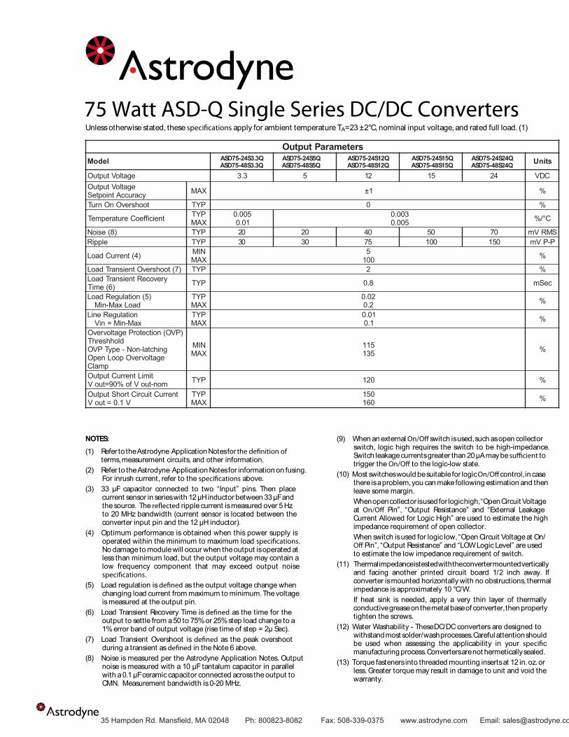
A
Unless otherwise stated, these apply for ambient temperature TA=23 ±2°C, nominal input voltage, and rated full load. (1)
NOTES:(1) Refer to the Astrodyne Application Notes for
terms,measurement circuits, and other information.(2) Refer to the Astrodyne Application Notes for information on fusing.
For inrush current, refer to the above.(3) 33 µF capacitor connected to two “Input” pins. Then place
current sensor in series with 12 µH inductor between 33 µF andthe source. The ripple current is measured over 5 Hzto 20 MHz bandwidth (current sensor is located between theconverter input pin and the 12 µH inductor).
(4) Optimum performance is obtained when this power supply isoperated within the minimum to maximum load No damage to module will occur when the output is operated atless than minimum load, but the output voltage may contain alow frequency component that may exceed output noise
.(5) Load regulation is as the output voltage change when
changing load current from maximum to minimum. The voltageis measured at the output pin.
(6) Load Transient Recovery Time is as the time for theoutput to settle from a 50 to 75% or 25% step load change to a1% error band of output voltage (rise time of step = 2µ Sec).
(7) Load Transient Overshoot is as the peak overshootduring a transient as in the Note 6 above.
(8) Noise is measured per the Astrodyne Application Notes. Outputnoise is measured with a 10 µF tantalum capacitor in parallelwith a 0.1 µF ceramic capacitor connected across the output toCMN. Measurement bandwidth is 0-20 MHz.
(9) When an external switch is used, such as open collectorswitch, logic high requires the switch to be high-impedance.Switch leakage currents greater than 20 µA may be totrigger the to the logic-low state.
(10) Most switches would be suitable for logic control, in casethere is a problem, you can make following estimation and thenleave some margin.When open collector is used for logic high, “Open Circuit Voltageat Pin”, “Output Resistance” and “External LeakageCurrent Allowed for Logic High” are used to estimate the highimpedance requirement of open collector.When switch is used for logic low, “Open Circuit Voltage at On/
Pin”, “Output Resistance” and “LOW Logic Level” are usedto estimate the low impedance requirement of switch.
(11) Thermal impedance is tested with the converter mounted verticallyand facing another printed circuit board 1/2 inch away. Ifconverter is mounted horizontally with no obstructions, thermalimpedance is approximately 10 °C/W.If heat sink is needed, apply a very thin layer of thermallyconductive grease on the metal base of converter, then properlytighten the screws.
(12) Water Washability - These DC/DC converters are designed towithstand most solder/wash processes. Careful attention shouldbe used when assessing the applicability in your cmanufacturing process. Converters are not hermetically sealed.
(13) Torque fasteners into threaded mounting inserts at 12 in. oz. orless. Greater torque may result in damage to unit and void thewarranty.
sretemaraPtuptuOledoM stinU
egatloVtuptu 3O .3 5 21 51 42 CDVegatloVtuptuO
ycaruccAtniopteS XA 1M %±
toohsrevOnOnru PT Y %0T
tneiciffeoCerutarepmeT PYTXAM
500.010.0
300.0500.0 C°/%
)8(esio PN YT 02 02 04 05 07 SMRVmelppi PR YT 03 03 57 001 051 P-PVm
)4(tnerruCdaoL NIMXAM
5001 %
)7(toohsrevOtneisnarTdao PL Y %2TyrevoceRtneisnarTdaoL
)6(emiT PY 8T . c0 eSm
)5(noitalugeRdaoLdaoLxaM-niM
PYTXAM
20.02.0 %
noitalugeReniLxaM-niM=niV
PYTXAM
10.01.0 %
)PVO(noitcetorPegatlovrevOdlohhserhT
gnihctal-noN-epyTPVOegatlovrevOpooLnepO
pmalC
NIMXAM
511531 %
timiLtnerruCtuptuOmon-tuoVfo%09=tuoV PY 0T 2 %1
tnerruCtiucriCtrohStuptuOV1.0=tuoV
PYTXAM
051061 %
ASD75-24S3.3Q ASD75-24S5Q ASD75-24S12Q ASD75-24S15Q ASD75-24S24QASD75-48S3.3Q ASD75-48S5Q ASD75-48S12Q ASD75-48S15Q ASD75-48S24Q
75 Watt ASD-Q Single Series DC/DC Converters
35 Hampden Rd. Mansfield, MA 02048 Ph: 800823-8082 Fax: 508-339-0375 www.astrodyne.com Email: [email protected]
snoitacificepSlareneGsledoMll sA tinU
noitcnuFFFO/NOetomeRleveLcigoLHGIH
niPFFO/NOevaeLronepO
NIM 0.3 CDV
tnerruCegakaeLlanretxE)9(hgiHcigoLrofdewollA XAM 02 Aµ
noitcetorPedoiDtupnIegatloV XAM 05 CDV
leveLcigoLWOLtupnI-otniPFFO/NOeiTro XAM 0.1 CDV
cigoLroftnerruCgnikniSwoL XAM 1 Am
taegatloVtiucriCnepO)01(niPFFO/NOyramirP
cigoLevitisoPcigoLevitageN
PYTPYT
6.55.1
CDVCDV
tnerruCeldI)FFOsieludoM( PYT 6 CDAm
rorre%1otemiTno-nru PT YT 8 ceSm
noitpOcigoLevitisoP NOeludoM-HGIHFFOeludoM-WOL
noitpOcigoLevitageN FFOeludoM-HGIHNOeludoM-WOL
mirTegatloVtuptuO
egnaRmirT NIMXAM 01± fo%
tuoVecnatsiseRtupn PI YT 01 mhOk
egatloVtiucriCnep PO YT 5.2 VgnisneSetomeRegatloVtuptuO
sporDegatloVmumixaMdaeLno XAM 5.0 CDV
noitalugeReniLgnisnesetomerrednu
PYTXAM
20.01.0 %
noitalugeRdaoLgnisnesetomerrednu
PYTXAM
50.02.0 %
timiLmirTdnaesneS
egatloVtuptuOmumixa XM AM 011 fo%tuoV
noitalosI*noitalosItuptuOottupnI
egakaeLAµ01sledomV42=monVsledomV84=monV
XAMXAM
0074451
CDVCDV
latnemnorivnEeroclleB,FBTMdetaluclaC
1esaC,1dohteM 000,000,1> rH
gnitarepOetalpesaBegnaRerutarepmeT
NIMXAM
04-001 C°
erutarepmeTegarotS NIMXAM
04-021 C°
)11(ecnadepmIlamreh PT YT 9 W/C°nwodtuhSlamrehT
erutarepmeTetalpesaB)tratseRotuA(
NIMPYT
001011 C°
lareneGnoisnemiDesa "C 05.0x"54.1x"82.2
gnidnePslavorppAycneg 0A 5906LUC/LUtiKgnitnuoMsissah 8C 1SM
stresnIgnitnuoMnoeuqroT XAM .zo.ni21
ni nP oitcnuF1 TUPNI-2 FFO/NO3 TUPNI+
T4 UPTUO-5 ESNES-6 MIRT
E7 SNES+T8 UPTUO+
* Absolute Maximum Ratings. Caution: Stresses in excess of the AbsoluteMaximum Ratings can cause permanent damage to the device (see Note 1).
Mechanical tolerances unless otherwise noted:
X.XX dimensions: ±0.020 inches
X.XXX dimensions: ±0.005 inches
75 Watt ASD-Q Single Series DC/DC Converters
35 Hampden Rd. Mansfield, MA 02048 Ph: 800823-8082 Fax: 508-339-0375 www.astrodyne.com Email: [email protected]

35 Hampden Rd. Mansfield, MA 02048 Ph: 800823-8082 Fax: 508-339-0375 www.astrodyne.com Email: [email protected]
100 WATT ASD SINGLE SERIES DC/DC CONVERTERS
Features4:1 Input voltage rangeHigh power densitySmall size 2.4” x 2.28” x 0.55”Excellent thermal performance with metal baseplateVolt-seconds clamp and fast over voltage protectionPulse-by-pulse current limiting, short circuit frequency
foldback, dead short shut downOver-temperature protectionAuto-softstartLow noiseIndustry-standard pinoutConstant frequency during normal operationRemote senseRemote ON/OFFSuper energy saving, 8 mA input idle currentOutput trim with very low temperature coefficientWater washable, wide humidity applicationGood shock and vibration dampingAvailable in both RoHS and Non-RoHS construction.
See ordering info below model selection chart.
Selection Chart
ModelInput Range
VDCIin
ADC VoutVDC
IoutADC
Min Max TYP
ASD100-24S3.3W 9 36 4.24 3.3 25
ASD100-24S5W 9 36 4.91 5 20
ASD100-24S12W 9 36 4.85 12 8.33
ASD100-24S15W 9 36 4.79 15 6.67
ASD100-24S24W 9 36 4.79 24 4.13
ASD100-48S3.3W 18 75 2.10 3.3 25
ASD100-48S5W 18 75 2.42 5 20
ASD100-48S12W 18 75 2.39 12 8.33
ASD100-48S15W 18 75 2.37 15 6.67
ASD100-48S24W 18 75 2.37 24 4.13
The 4:1 Input Voltage 100 W single ASD Series of DC/DC converters provide precisely regulated dc outputs. The output voltage is fully isolated from the input, allowing the output to be positive or negative polarity and with various ground connections. The ASD Series utilizes an
The 4:1 Input Voltage 100 Watt ASD Series includes remote sensing, output trim, and remote ON/OFF. Threaded-through holes are provided to allow easy mounting or add a heat sink for extended temperature use.
Description
Default ON/OFF logic is positive.Add -N to the model number to order negative On/Off logic.To order RoHS, add (RoHS) to part number.
insulated metal substrate design in an industry standard 1/2 brick case size to meet the most rigorous require- ments of COTS and thermally challenging industrial applications.
100 WATT ASD SINGLE SERIES DC/DC CONVERTERS
Input ParametersModel ASD100-24S3.3W ASD100-24S5W ASD100-24S12W ASD100-24S15W ASD100-24S24W Units
Voltage RangeMINTYPMAX
92436
V
Input Overvoltage (100 ms) MAX 50 V
Input Ripple Rejection (120Hz) TYP 60 dB
Undervoltage Lockout Yes
Input Reverse Voltage Protection Yes
Input Current No Load 100% Load
TYPTYP
354.24
354.91
354.85
354.79
354.79
mAA
Inrush Current MAX 0.5 A2s
Reflected Ripple, 12µHSource Impedance (3) TYP 30 mA P-P
Efficiency TYP 79 85 86 83 87 %
Switching Frequency TYP 260 kHz
Recommended Fuse (2) A
Input ParametersModel ASD100-48S3.3W ASD100-48S5W ASD100-48S12W ASD100-48S15W ASD100-48S24W Units
Voltage RangeMINTYPMAX
184875
V
Input Overvoltage (100 mSec) MAX 80 V
Input Ripple Rejection (120Hz) TYP 60 dB
Undervoltage Lockout Yes
Input Reverse Voltage Protection Yes
Input Current No Load 100% Load
TYPTYP
252.10
252.42
252.39
252.37
252.37
mAA
Inrush Current MAX 0.5 A2s
Reflected Ripple, 12µHSource Impedance (3) TYP 30 mA P-P
Efficiency TYP 81 85 88 88 89 %
Switching Frequency TYP 260 kHz
Recommended Fuse (2) A
Unless otherwise stated, these specifications apply for baseplate temperature TB=23±2ºC, nominal input voltage, and rated full load. (1)
* Absolute Maximum Ratings. Caution: Stresses in excess of the Absolute Maximum Ratings can cause permanent damage to the device (see Note 1.)
35 Hampden Rd. Mansfield, MA 02048 Ph: 800823-8082 Fax: 508-339-0375 www.astrodyne.com Email: [email protected]

100 WATT ASD SINGLE SERIES DC/DC CONVERTERS
Output ParametersModel ASD100-24S3.3W
ASD100-48S3.3WASD100-24S5WASD100-48S5W
ASD100-24S12WASD100-48S12W
ASD100-24S15WASD100-48S15W
ASD100-24S24WASD100-48S24W
Units
Output Voltage 3.3 5 12 15 24 V
Output VoltageSetpoint Accuracy MAX ±1 %
Turn On Overshoot Min-Max Load TYP 0 %
Temperature Coefficient TYPMAX
0.0050.01
0.0030.005
0.0030.005
0.0030.005
0.0030.005 %/ºC
Noise (8) TYPTYP
7520
7520
15060
15060
250100
mV P-PmV RMS
Load Current (4) MINMAX
2.525
220
0.8338.33
0.6676.67
0.4134.13 A
Load Transient Overshoot (7) TYP 3 %
Load Transient Recovery Time (6) TYP 200 µs
Load Regulation (5) Min-Max Load
TYPMAX
0.020.2 %
Line Regulation Vin = Min-Max
TYPMAX
0.010.1 %
Overvoltage Protection (OVP)ThreshholdOVP Type - Non-latchingOpen Loop Overvoltage Clamp
MINMAX
115135 %
Output Current LimitVout = 90% of Vout-nom TYP 120 %
Output Short Circuit CurrentVout = 0.25V
TYPMAX
140150 %
Notes:(1) Refer to the Application Notes for the definition of terms,
measurement circuits, and other information.(2) Refer to the Application Notes for information of fusing.
For inrush current, refer to the specifications above.(3) 33µF capacitor connected between the two “Input” pins. Then
insert current sensor in series with 1.0µH inductor between 100µF and the source. The reflected ripple current is measured over a 5 Hz to 20 MHz bandwidth. (current sensor is located between the converter input pin and the 1.0 µH inductor)
(4) Optimum performance is obtained when this power supply is operated within the minimum to maximum load specifications. No damage to the module will occur when the output is operated at less than minimum load, however, below minimum load the dynamic response will degrade. Operation below minimum load is not recommended.
(5) Load regulation is defined as the output voltage change when changing load current from a maximum to minimum.
(6) Load Transient Recovery Time is defined as the time for the output to settle from a 50% to 75% step load change to a 1% error band (rise time of step = 2µs).
(7) Load Transient Overshoot is defined as the peak overshoot during a transient as defined in the Note 6 above.
(8) Noise is measured per the Application Notes. Output noise is measured with a 10µF tantalum capacitor in parallel with a 0.1µF ceramic capacitor connected across the output pins. Measurement bandwidth is 0-20MHz.
(9) When an external ON/OFF switch is used, such as open collector switch, logic high requires the switch to be high-impedance. Switch leakage currents greater than 10µA may be sufficient to trigger the ON/OFF to the logic-low state.
(10) Most switches would be suitable for the logic ON/OFF control. In case there is a problem you can make the following estimations and then leave some margin.
When open collector is used for logic high, “Open Circuit Voltage at ON/OFF Pin”, “Output Resistance” and “External Leakage Current Allowed for Logic High” are used to estimate the high impedance requirement of open collector.
When switch is used for logic low, “Open Circuit Voltage at ON/OFF Pin”, “Output Resistance” and “LOW Logic Level” are used to estimate the low impedance requirement of the switch.
(11) Thermal impedance is tested with the converter mounted vertically and facing another printed circuit board 1/2 inch away. If converter is mounted horizontally with no obstruction, thermal impedance is approximately 8°C/W.
(12) Water Washability - These DC/DC converters are designed to withstand most solder/wash processes. Careful attention should be used when assessing the applicability in your specific manufacturing process. Converters are not hermetically sealed.
(13) Torque fasteners into threaded mounting inserts at 12 in.lbs. or less. Greater torque may result in damage to unit and void the warranty.
(14) Input impedance on these units needs to be kept to a minimum. The 9-36Vdc DC units need a maximum input impedance of 0.2 Ohms and the 18-75Vdc DC units need a maximum input impedance of 0.8 Ohms. In order to support this requirement, the 9-36Vdc DC units need 25 µF of capacitance (low ESR) for every 1.0 µH of inductance between the power source and the DC/DC converter. The 18-75Vdc DC units need 1.7µF of capacitance (low ESR) for every 1.0 µH of inductance between the power source and the DC/DC converter. Inductance includes all sources and should take into account input power lines.
(15) RoHS Compliance: See Astrodyne Website www.astrodyne.com for the complete
RoHS Compliance statement and Application Notes. The RoHS marking is as follows.
35 Hampden Rd. Mansfield, MA 02048 Ph: 800823-8082 Fax: 508-339-0375 www.astrodyne.com Email: [email protected]

100 WATT ASD SINGLE SERIES DC/DC CONVERTERS
General SpecificationsAll Models UnitsON/OFF FunctionHIGH Logic Level or Leave ON/OFF Pin Open MIN 3.0 VDC
External Leakage Current Allowed for Logic High (9) MAX 10 µA
Input Diode Protection Voltage MAX 50 VDC
LOW Logic Level or Tie ON/OFF Pin to -INPUT MAX 1.0 VDC
Sinking Current for Logic Low MAX 500 µA
Open Circuit Voltage at ON/OFF Pin (10)Positive LogicNegative Logic
TYPTYP
2.31.5
VDCVDC
Output Resistance TYP 3 k Ω
Idle Current(Module is OFF) TYP 8 mADC
Turn-on Time to 1% error TYP 60 ms
Positive Logic Option HIGH - Module ONLOW - Module OFF
Negative Logic Option HIGH - Module OFFLOW - Module ON
Output Voltage Remote SensingMaximum Voltage Drops on Leads MAX 10 %
Line Regulation under remote sensing
TYPMAX
0.020.1 %
Load Regulation under remote sensing
TYPMAX
0.050.2 %
Output Voltage Trim
Trim Range MINMAX
-10+10 % of Vout
Input Resistance TYP 10 kΩ
Open Circuit Voltage TYP 2.5 V
Trim LimitMaximum Output Voltage MAX 110 % of Vout
IsolationInput to Output Isolation 10µA LeakageVnom = 24VVnom = 48V
MAXMAX
7001544
VDCVDC
Input to Output Resistance MIN 10 MΩ
Input to Output Capacitance TYP 1600 pF
EnvironmentalCalculated MTBF, Bellcore Method 1, Case 1 >1,000,000 h
Baseplate Operating Temperature Range
MINMAX
-40100 ºC
Storage Temperature MINMAX
-40120 ºC
Thermal Impedance (11) TYP 7 ºC/W
Thermal Shutdown BaseplateTemperature (Auto Restart)
MINTYP
100110 ºC
Pin Name Pin Dia. Pin Dia.
1 -INPUT 0.08” 0.04”
2 CASE 0.04” 0.04”
3 ON/OFF 0.04” 0.04”
4 +INPUT 0.08” 0.04”
5 -OUTPUT 0.08” 0.08”
6 -SENSE 0.04” 0.04”
7 TRIM 0.04” 0.04”
8 + SENSE 0.04” 0.04”
9 + OUTPUT 0.08” 0.08”
TOLERANCE: ALL DIMENSIONS ARE TYPICAL IN INCHES UNLESS OTHERWISE NOTED:
X.XX ±0.020
X.XXX ±0.005
General SpecificationsAll Models UnitsGeneralUnit Weight TYP 4.6/114 oz/g
Case Dimension 2.4” x 2.28” x 0.55”
Torque on Mounting Inserts MAX 12 in. lbs.
Agency Approvals
UL, TUV Pending for UL60950EN60950 (TUV)
Chassis Mounting Kit MS21
35 Hampden Rd. Mansfield, MA 02048 Ph: 800823-8082 Fax: 508-339-0375 www.astrodyne.com Email: [email protected]

150 Wat t , H igh E f f i c iency, Quar te r Br ick DC/DC Conver te r A S D 1 5 0 Q B s e r i e s
WWW.ASTRODYNE.COMASTRODYNE USA: 1-800-823-8082ASTRODYNE PACIFIC: 886-2-26983458
ABSOLUTE MAXIMUM RATINGS (MIN TO MAX.)
Input Voltage (+In to -In) 24Vin: -0.3 to 36VDC (50VDC <100mS) 48Vin: -0.3 to 75VDC (100VDC <100mS) Logic ON/OFF Voltage -0.3 to 5V (ON/OFF to -In) Storage Temperature -40 to +125°C Storage Humidity 10 to 95% Operating Temperature (Note 5) -40 to 100°C Operating Humidity 30 to 95% Output Power 150 Watts
INPUT SPECIFICATIONS
Input Operation Voltage: See Model Selection Chart PG. 1 Input Current FL @ Nom Vin, FL See Model Selection Chart PG. 1 Inrush Transient 1A²s Input Reflected Ripple Current 40mAp-p, typ. (60mA max.) Input Ripple Rejection 60dB@120Hz Input Under Voltage Protection (24Vin/48Vin) Turn-on Threshold: 17.5-18V/34-36V max. Turn-off Threshold: 15.5-16V/30-32V typ. Hysteresis: 1-1.5V/2.0V typ.
OUTPUT SPECIFICATIONS
Output Voltage & Current See Model Selection Chart PG. 1 Output Set Point (Vo,set; Note 6) See Model Selection Chart PG. 1 Output Voltage Tolerance Band +/-3% Load/Load Regulation 20mV max. Temperature Coefficient +/-0.02%/°C, -40 to 100°C Ripple/Noise p-p max. (Note 1) 3.3, 5Vo: 70mV; 12Vo: 120mV Dynamic Response (Vo, Set): 6% max., Nom. Vin, Tb=25°C (Note 3) Peak Deviation 300uS duration outside of Vo set Settling Time +/-1% error band Over Voltage Protection 112-140% of Output, Io=0.5A Over Temperature Protection 100-115°C, auto recover @ 90°C See Fig. 3 for location definition External Capacitance 660 to 5000uF max. Short Circuit Protection (ISC) See Model Selection Chart PG. 1 Current Limit (Note 2) 105-145% of Rated Load Efficiency (Nom. Vin, 80% Load) See Model Selection Chart PG. 1
STRUCTURAL DYNAMICS
Vibration (Note 4) Shock 20g, 166in/sec, Square Wave
ISOLATION SPECIFICATIONS
Input-Output, Input-Case 1500VDC, 60S Output-Case 500VDC, 60S Input-Output Capacitance 2000pF Isolation Resistance 100MΩ @ Tb=25°C & 70%RH Output to Baseplate-500VDC
GENERAL SPECIFICATIONS
MTBF 1.8Mhrs Tb=40°C, 80%FL Weight 2.29 oz (65g) Dimensions 2.28” x 1.45” x 0.5” (57.91 x 36.83 x 12.7mm)
CONTROL SPECIFICATIONS
Logic ON/OFF Remote Positive Logic: Off State Voltage: 0.8V max. On State Voltage: 2V min. Negative Logic (optional): Off State Voltage: 2V min. On State Voltage: 0.8V max. Turn-On Time 40mS, Vo=90% of Vo, set Trim Adjustment Range 90-110% See TRIM CIRCUITS Figs 1 & 2
NOTES
1.2.Bandwidth 5Hz to 20MHz and with filter 0.1uF MLCC Nominal Vin; Io=FL; Tb=25°C; Output Capacitor with 220uF*3.2. Current Limit inception point Vo=90% of Vo, set.3. 25%-50%-75% load, Δ Io/ Δ t=0.1A/uS; w/o Cap. 220uF*3 each4. Sine Wave, 10-55Hz (Sweep for 1 min.), Amplitude 0.825mm Constant (Max. 5g) X, Y. Z 1 Hour each, at No Operation5. Temperature measurement shall be taken from the baseplate (Tb). See Fig. 3 for location definition .6. Tb=25°C, Nominal Vin, Full Load (FL)
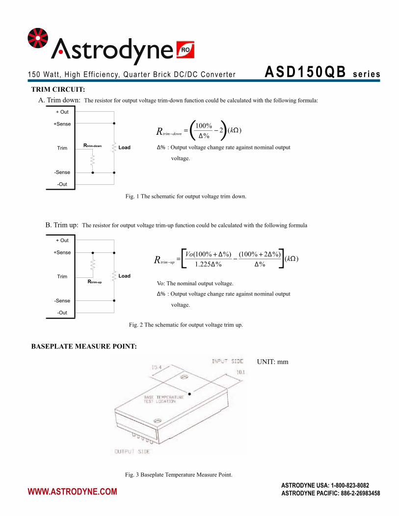
150 Wat t , H igh E f f i c iency, Quar te r Br ick DC/DC Conver te r A S D 1 5 0 Q B s e r i e s
WWW.ASTRODYNE.COMASTRODYNE USA: 1-800-823-8082ASTRODYNE PACIFIC: 886-2-26983458
TRIM CIRCUIT: A. Trim down: The resistor for output voltage trim-down function could be calculated with the following formula:
+ Out
+Sense
Trim
-Sense
-Out
Rtrim-down Load
Fig. 1 The schematic for output voltage trim down.
B. Trim up: The resistor for output voltage trim-up function could be calculated with the following formula
+ Out
+Sense
Trim
-Sense
-Out
Rtrim-up
Load
Fig. 2 The schematic for output voltage trim up.
BASEPLATE MEASURE POINT:
Fig. 3 Baseplate Temperature Measure Point.
UNIT: mm
Δ% : Output voltage change rate against nominal output
voltage.
Vo: The nominal output voltage.
Δ% : Output voltage change rate against nominal output
voltage.
)(2%%100
Ω−∆
=−
kR downtrim
)(%
%)2%100(%1.225
%)%100(Ω
∆∆+
−∆
∆+=
−kVoR uptrim
( )
[ ]

150 Wat t , H igh E f f i c iency, Quar te r Br ick DC/DC Conver te r A S D 1 5 0 Q B s e r i e s
WWW.ASTRODYNE.COMASTRODYNE USA: 1-800-823-8082ASTRODYNE PACIFIC: 886-2-26983458
EFFICIENCY CURVE:
76
78
80
82
84
86
88
90
92
94
0% 10% 20% 30% 40% 50% 60% 70% 80% 90% 100%
18 Vin
24 Vin
36 Vin
Efficiency (%)
Output Power ,max = 150W (%)
EFFICIENCY CURVE :
6870727476788082848688909294
0%
Io,max = 45.45 A
Effi
cien
cy %
36 Vin48 Vin75 Vin
10% 20% 30% 100%90%80%70%60%50%40%
24VIN, 3.3VOUT
48VIN, 3.3VOUT

150 Wat t , H igh E f f i c iency, Quar te r Br ick DC/DC Conver te r A S D 1 5 0 Q B s e r i e s
WWW.ASTRODYNE.COMASTRODYNE USA: 1-800-823-8082ASTRODYNE PACIFIC: 886-2-26983458
EFFICIENCY CURVE :
6870727476788082848688909294
Io,max = 30 A
Effi
cien
cy %
36 Vin48 Vin75 Vin
0% 10% 20% 30% 100%90%80%70%60%50%40%
48VIN, 5.0VOUT
EFFICIENCY CURVE:
78
80
82
84
86
88
90
92
94
0% 10% 20% 30% 40% 50% 60% 70% 80% 90% 100%
18 Vin
24 Vin
36 Vin
Efficiency (%)
Output Power ,max = 150W (%)
24VIN, 5.0VOUT

150 Wat t , H igh E f f i c iency, Quar te r Br ick DC/DC Conver te r A S D 1 5 0 Q B s e r i e s
WWW.ASTRODYNE.COMASTRODYNE USA: 1-800-823-8082ASTRODYNE PACIFIC: 886-2-26983458
EFFICIENCY CURVE:
76
78
80
82
84
86
88
90
92
94
0% 10% 20% 30% 40% 50% 60% 70% 80% 90% 100%
18 Vin
24 Vin
36 Vin
Efficiency (%)
Output Power ,max = 150W (%)
24VIN, 12VOUT
EFFICIENCY CURVE :
6870727476788082848688909294
Io,max = 12.5 A
Effi
cien
cy %
36 Vin48 Vin75 Vin
0% 10% 20% 30% 100%90%80%70%60%50%40%
48VIN, 12VOUT

150 Wat t , H igh E f f i c iency, Quar te r Br ick DC/DC Conver te r A S D 1 5 0 Q B s e r i e s
WWW.ASTRODYNE.COMASTRODYNE USA: 1-800-823-8082ASTRODYNE PACIFIC: 886-2-26983458
DERATING CURVE:
Baseplate Temperature ( )
Output Power (%)

150 Wat t , H igh E f f i c iency, Quar te r Br ick DC/DC Conver te r A S D 1 5 0 Q B s e r i e s
WWW.ASTRODYNE.COMASTRODYNE USA: 1-800-823-8082ASTRODYNE PACIFIC: 886-2-26983458
OUTLINE DRAWING:
OUTLINE PIN ASSIGNMENT: Pin Number
1 Input (-)
2 On/Off Control
3 Input (+)
4 Output (+)
5 Output (+)
6 Sense (+)
7 Trim
8 Sense (-)
9 Output (-)
10 Output (-)
Signal name: 3.3 & 5Vo Signal name: 12Vo
Input (-)
On/Off Control
Input (+)
Output (+)
Sense (+)
Trim
Sense (-)
Output (-)
No Pin
No Pin

High Outpu t Power, H igh E f f i c iency DC/DC Conver te r M V 2 4 - 2 8 - 6 0 0 S
WWW.ASTRODYNE.COMASTRODYNE USA: 1-800-823-8082ASTRODYNE PACIFIC: 886-2-26983458
Industry Standard 4.59” x 2.4” x 0.5” Package
High Power Density up to 109.29W/ Inch ³
High Typical Efficiency of 91%
Low Output Noise
Metal Baseplate
Thermal Protection
Over Voltage and Over Current Protection
Output Under Voltage Protection
Adjustable Output Voltage
Remote Sense
Auxiliary Voltage of 8V, +/-1V
I.O.G (DC Good): Open Collector Output
Remote ON/OFF Control
Model Number Output Voltage Output Amps Input Range Max. Iin FL Efficiency Max Output Power
MV24-28-600S 28 VDC 21.5 18-36 VDC 28.9A 91% 600 Watts
DESCRIPTION:The MEGAVERTER® MV24-28-600S dc/dc converter is a high density, feature rich module packaged in the industry standard “full brick” size (2.4 x 4.59 x 0.5 inches) for circuit board mounting. It is designed for use in a 24/28 Vdc (18-36Vdc) input applications where large blocks of DC power are required. The MV24-28-600S utilizes an insulated metal substrate and is therefore well suited for the most rigorous requirements of COTS and thermally challenging industrial applications.
High Outpu t Power, H igh E f f i c iency DC/DC Conver te r M V 2 4 - 2 8 - 6 0 0 S
WWW.ASTRODYNE.COMASTRODYNE USA: 1-800-823-8082ASTRODYNE PACIFIC: 886-2-26983458
ABSOLUTE MAXIMUM RATINGS (MIN TO MAX.)
Input Voltage (+In to -In) -0.3 to 50VDC (<100mS) -0.3 to 36VDC (Continuous) Storage Temperature -55 to +125°C Storage Humidity 10 to 95% Operating Temperature -40 to 100°C Temperature measurement shall be taken from the baseplate (Tb). See Fig. 3 for location definition Operating Humidity 30 to 95%
INPUT SPECIFICATIONS
Input Operation Voltage: 18-36 VDC Input Current FL 28.9A max. @ 24Vin, Full Load (FL) Inrush Transient 2A²s Input Ripple Rejection 60dB@120Hz
OUTPUT SPECIFICATIONS
Output Voltage 28VDC Output Current (Io, max.) 21.5A (Note 1) Output Set Point (Vo,set) 27.95-28.05V @ Tb=25°C, 24Vin, FL Output Voltage Accuracy 27.72-28.28 @ 24Vin, FL Load Regulation (0% to FL) +/-0.2%, max. Line Regulation (HL-LL) +/-0.2%, max. Temperature Coefficient +/-0.02%/°C, -40 to 100°C Ripple/Noise 250mV p-p max. (Note 2) Dynamic Response: Peak Deviation 3%Vo, set (Note 4) Settling Time 300uS Over Voltage Protection 115-135% of Output, Io=0.5A Output Under Voltage Protection 12V, Output Overload & Short CircuitOver Temperature Protection 105-115°C, Auto Recover @ 100°C Current Limit 105-140% of Rated Load (Note 3) Efficiency 91% @ 24Vin, 28Vo, 80%L Tb=25°C
ISOLATION SPECIFICATIONS
Input-Output, Input-Case 1500VDC, 60S Output-Case 500VDC, 60S Input-Output Capacitance 2000pF Isolation Resistance 100MΩ @ Tb=25°C & 70%RH Output to Baseplate-500VDC
STRUCTURAL DYNAMICS
Vibration (Note 5) Shock 20g, 166in/sec, Square Wave
GENERAL SPECIFICATIONS
MTBF 1.2Mhrs Tb=40°C, 80%FL, 24Vin Weight 7.94 oz (225g) Dimensions 4.59” x 2.4” x 0.5” (116.59 x 60.96 x 12.7mm)
CONTROL SPECIFICATIONS
Turn-On Time 200mS @ 80%FL, max. Vo with ± 1%Vo set Trim Adjustment Range 60-100% with Cap, 440uF/35V Tb=25°C See TRIM CIRCUITS Figs 1 & 2
NOTES
1.At Vo = 28V. If Vo > 28V, Output Power (Po) should be ≤ 602W2.Bandwidth 5Hz to 20MHz and with filter 0.1uF MLCC series 100Ω min. Output Capacitor: 220uF*2, Tc≥20°C, 220uF*4, Tc≤-20°C.3. Current Limit inception point Vo=90% of Vo, set @ Tb=25°C.4. 25%-50%-75% load, 0.1A/uS; With Cap. 440uF/35V Tb=25°C, 24Vin5. Sine Wave, 10-55Hz (Sweep for 1 min.), Amplitude 0.825mm Constant (Max. 0.5g) X, Y. Z 1 Hour each, at No Operation
All specifications are typical at nominal input, full load, and 25DegC unless otherwise noted
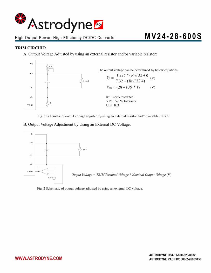
High Outpu t Power, H igh E f f i c iency DC/DC Conver te r M V 2 4 - 2 8 - 6 0 0 S
WWW.ASTRODYNE.COMASTRODYNE USA: 1-800-823-8082ASTRODYNE PACIFIC: 886-2-26983458
TRIM CIRCUIT: A. Output Voltage Adjusted by using an external resistor and/or variable resistor:
+S
-V
+V
-S
TR IM
Load
VR
R t
Fig. 1 Schematic of output voltage adjusted by using an external resistor and/or variable resistor.
B. Output Voltage Adjustment by Using an External DC Voltage:
+ S
-V
+ V
-S
T R IM
L o a d
D C
Fig. 2 Schematic of output voltage adjusted by using an external DC voltage.
The output voltage can be determined by below equations:
)32.4//(7. 23. 4 ))32//(1.225 *
RtRV t
f+
= (V)
fout VVR) *V ( 82 += (V)
Rt: +/-5% tolerance VR: +/-20% tolerance Unit: KΩ
Output Voltage = TRIM Terminal Voltage * Nominal Output Voltage (V)

High Outpu t Power, H igh E f f i c iency DC/DC Conver te r M V 2 4 - 2 8 - 6 0 0 S
WWW.ASTRODYNE.COMASTRODYNE USA: 1-800-823-8082ASTRODYNE PACIFIC: 886-2-26983458
BASEPLATE MEASURE POINT:
Fig. 3 Baseplate Temperature Measurement Point.
UNIT: mm
DERATING CURVE:
100%
80%
60%
40%
20%
0%
-40 -20 0 20 40 60 80 100
Baseplate Temperature (°C)
Output Power (%)

High Outpu t Power, H igh E f f i c iency DC/DC Conver te r M V 2 4 - 2 8 - 6 0 0 S
WWW.ASTRODYNE.COMASTRODYNE USA: 1-800-823-8082ASTRODYNE PACIFIC: 886-2-26983458
OUTLINE DRAWING:

500 Wat t , H igh E f f i c iency, AC/DC Power Modu le S M V- 2 8 - 5 0 0
WWW.ASTRODYNE.COMASTRODYNE USA: 1-800-823-8082ASTRODYNE PACIFIC: 886-2-26983458
Miniature 4.59” x 2.4” x 0.5.” Size
High Power Density up to 90.78W/ Inch ³
High Typical Efficiency of 88.5% at 230VAC
Low Output Noise
Metal Baseplate
Thermal Protection
Over Voltage Protection
Current Limit/Short Circuit Protection
Adjustable Output Voltage 60-120% of Vo, Set
Remote Sense
Power On Signal (ENA) Open Collector (10mA sink current). Low (ON) when output is present
Model Number Output Voltage Output Amps Input Range Max. Iin FL Efficiency (Tb=25°C) O/P Set Point
SMV-28-500 28 VDC 18 85-265 VAC 6.2A 88.5% 27.44-28.56VDC
DESCRIPTION:The SMV-28-500 is a high power density and high efficiency AC/DC converter module which utilizes a metal baseplate, planar transformers and surface mount construction to produce up to 500W of output power and is therefore well suited for the most rigorous requirements of COTS and thermally challenging industrial applications.
All specifications are typical at nominal input, full load, and 25DegC unless otherwise noted

500 Wat t , H igh E f f i c iency, AC/DC Power Modu le S M V- 2 8 - 5 0 0
WWW.ASTRODYNE.COMASTRODYNE USA: 1-800-823-8082ASTRODYNE PACIFIC: 886-2-26983458
ABSOLUTE MAXIMUM RATINGS (MIN TO MAX.)
Input Voltage (AC(L) to AC(N) 300 VAC with No Damage Power Factor Correction 0.95 min HL-LL and Full Load Storage Temperature -55 to +125°C Storage Humidity 10 to 95% Operating Temperature (Note 5) -40 to 100°C Operating Humidity 20 to 95% Output Power 500 Watts
INPUT SPECIFICATIONS
Input Operation Voltage: 85-265 VAC Input Frequency 47-63 Hz Input Current FL @ 100 Vin, FL 6.2A Inrush Current (Note 3) 40A @ 265VAC
OUTPUT SPECIFICATIONS
Output Voltage & Current See Model Selection Chart PG. 1 Output Set Point See Model Selection Chart PG. 1 Output Voltage Adjustment Range 16.8-33.6VDC @ FL Load Regulation 56mV typ. NL-FL Line Regulation 56mV typ. HL-LL Ripple/Noise p-p max. (Note 1) 280mV Dynamic Response (Note 6) 25% - 50% - 75% Load Peak Deviation: 3% Vo, set Settling Time 300uS Current Limit (Note 2) 105-140% of Rated Load Over Voltage Protection 125-145% Vo, set, Io=0.5A, clamp Over Temperature Protection Shutdown: 110°C typ. Auto Recovery: 90°C min. Efficiency (Tb=°C) 86.5% @ 110 Vin, FL 88.5% @ 230Vin, FL See Fig. 4 EFFICIENCY CURVE
STRUCTURAL DYNAMICS
Vibration (Note 4) Shock 196.1mS²
ISOLATION SPECIFICATIONS
Input-Output 3000VAC, 60S Input-Case 2500VAC, 60S Output-Case 1500VDC, 60S Input-Output Capacitance 2000pF Isolation Resistance 100MΩ @ Tb=25°C & 70%RH Output to Baseplate-500VDC
GENERAL SPECIFICATIONS
MTBF TBD Weight TBD Dimensions 4.59” x 0.5” x 2.4” (116.8 x 12.7 x 61mm)
CONTROL SPECIFICATIONS
Turn-on Time 3S max., 90% Vo, set, FL Trim Adjustment Range 60-120% with Cap. 940uF/35V, Tb=25°C See Fig. 1 TRIM CiRCUIT
NOTES
1.2.Bandwidth 5Hz to 20MHz and with filter 4.7nF MLCC series 50Ω min. Output Capacitor: 470uF*2, TC≥ -20°C, 470uF*4, TC≤ -20°C.2. Current Limit inception point Vo=90% of Vo, set @ Tb-25°C; Auto recovery.3. Turn on @ 265Vin, External Components are needed for operation Refer to Fig. 3 for application circuit.4. Sine Wave, 10-55Hz (Sweep for 1 min.), Amplitude 0.825mm Constant (Max. 0.5g) X, Y. Z 1 Hour each, at No Operation5. Temperature measurement shall be taken from the baseplate (Tb). See Fig. 2 for location definition .6. 0.1A/uS; with cap 940uF/35V, Tb=25°C, Vin=200VAC

500 Wat t , H igh E f f i c iency, AC/DC Power Modu le S M V- 2 8 - 5 0 0
WWW.ASTRODYNE.COMASTRODYNE USA: 1-800-823-8082ASTRODYNE PACIFIC: 886-2-26983458
TRIM CIRCUIT: Output Voltage Adjusted by using external resistor and/or variable resistor:
R=33Kohm and VR=20Kohm for 60% to 120% of Vo,set
Fig1 The schematic of output voltage adjusted by using external resistor and/or variable resistor.
BASEPLATE MEASURE POINT:
Fig2 Baseplate Temperature Measure Point.

500 Wat t , H igh E f f i c iency, AC/DC Power Modu le S M V- 2 8 - 5 0 0
WWW.ASTRODYNE.COMASTRODYNE USA: 1-800-823-8082ASTRODYNE PACIFIC: 886-2-26983458
APPLICATION CIRCUIT:
Fig. 3 Application Circuit.
AstrodyneSMV-28-500
EFFICIENCY CURVE:

500 Wat t , H igh E f f i c iency, AC/DC Power Modu le S M V- 2 8 - 5 0 0
WWW.ASTRODYNE.COMASTRODYNE USA: 1-800-823-8082ASTRODYNE PACIFIC: 886-2-26983458
OUTLINE DRAWING:
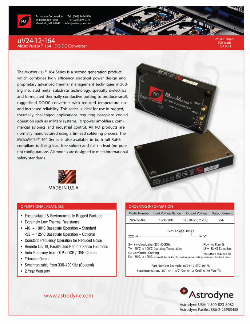
RO
24 VDC Input300 Watts
3/4 Brick
The MICROVERTER 164 Series is a second generation product which combines high eciency electrical power design and proprietary advanced thermal management techniques includ- ing insulated metal substrate technology, specialty dielectrics and formulated thermally conductive potting to produce small, ruggedized DC/DC converters with reduced temperature rise and increased reliability. This series is ideal for use in rugged, thermally challenged applications requiring baseplate cooled operation such as military systems, RF/power ampliers, com-mercial avionics and industrial control. All RO products are normally manufactured using a tin-lead soldering process. The MICROVERTER 164 Series is also available in both full RoHS compliant (utilizing lead free solder) and full tin-lead (no pure tin) congurations. All models are designed to meet international safety standards.
MADE IN U.S.A.
uV24-12-164MICROVERTER 164 DC-DC Converter
OPERATIONAL FEATURES
XXX YY
C= Conformal Coating (Consult the factory for output power rating)
Part Number Example: uV24-12-STC-164RL
Synchronization, -55 C to 100
uV24-12-XXX-164YY
no sux is required for standard tin-lead nish
ORDERING INFORMATION Model Number Input Voltage Range Output Voltage Output Current
Astrodyne Corporation Tel: (508) 964-630035 Hampden Road Fx: (508) 339-0375
30www.astrodyne.com
Astrodyne USA: 1-800-823-8082
C
M
Y
CM
MY
CY
CMY
K
uV24-12-164_r100315 1.pdf 1 6/29/2010 10:11:34 AM

uV24-12-164
ABSOLUTE MAXIMUM RATINGS Parameter Option Minimum Maximum Units Conditions
-0.3 36 Continuous
-0.3 50 100ms max.
-0.3 6.0
1500
1500
500
Storage Temperature
Standard -40 110
T -55 110
-55 125
Operating Temperature
Standard -40 100
T -55 100
-55 125
Soldering Temperature 260 < 5 sec
ELECTRICAL SPECIFICATIONS Input Minimum Typical Maximum Units Conditions
18 24 / 28 36
Maximum Input Current19.4 Adc
19.8 Adc
Input Ripple Rejection 60 f = 120Hz
Output Minimum Typical Maximum Units Conditions
11.88 12.01 12.12
0.05 0.2 %
0.05 0.2 %
0.02 Tc min to Tc max
120 240
360
Rated Current 0 25 A
105 115 130 % Rated
Short Circuit Current 170 % Rated
Transient Response Deviation 480 20-80% Rated Current, 0.5A/µs
Transient Response Settling Time 200 µs 20-80% Rated Current, 0.5A/µs
88.0 %
Isolation Minimum Typical Maximum Units Conditions
Input-to-Output Isolation 1500 Consult factory for procedure
Input-to-Case Isolation 1500
Output-to-Case Isolation 500
Input-to-Output Capacitance 2500 pF
Input-to-Output Resistance 10 M Ohm
30
www.astrodyne.com
Astrodyne USA: 1-800-823-8082
C
M
Y
CM
MY
CY
CMY
K
uV24-12-164_r100315 2.pdf 1 6/29/2010 11:06:25 AM
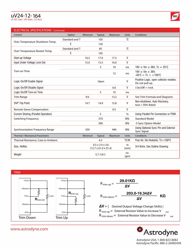
uV24-12-164
TRIM
ELECTRICAL SPECIFICATIONS Continued
Control Option Minimum Typical Maximum Units Conditions
Over Temperature Shutdown Temp.Standard and T 105
130
Over Temperature Restart Temp.Standard and T 85
105
16.5 17.0 17.5
15.0 15.5 16.0
Turn-on Time5 10 ms
12 ms
Open Do not pull up.
0.6 I On/O = 1mA.
5 10 ms
Trim Range 9.6 13.2 See Trim Formula and Diagrams
14.7 14.9 15.8 Iout = 50% Rated
Remote Sense Compensation 0.5
5 %
Switching Frequency 370 Standard Model
300 -S Sync Option Model
Synchronization Frequency Range 330 440 Sync Signal
Thermal / Mechanical Parameters Minimum Typical Maximum Units Conditions
Thermal Resistance, Case to Ambient 4.2
0.5 x 2.4 x 3.6(12.7 x 61.0 x 91.4)
in(mm)
5.7 (161)oz.
(gm)
Rtrim-dn
+Out
+Sense
Trim
-Sense
-Out
LoadRtrim-up
+Out
+Sense
Trim
-Sense
-Out
Load
Trim Down Trim Up
= | Desired Output Voltage Change (Volts) |R trim-up = External Resistor Value to Increase V out
R trim-down = External Resistor Value to Decrease V out
R trim-up =
Trim Down Trim Up
R trim-down =
30
www.astrodyne.com
Astrodyne USA: 1-800-823-8082
C
M
Y
CM
MY
CY
CMY
K
uV24-12-164_r100315 3.pdf 1 6/29/2010 11:06:34 AM

uV24-12-164
OUTLINE DRAWING Dimensions in Inches
NOTES
2.40
0.28 DIA. X 0.19 DEEP4 PLACES
0.50
0.040 DIA. PIN BRASS ALLOY7 PLACES
0.20 MIN.
NOTE:Pin finish is gold over nickel, JESD972nd level interconnect category e4.
* 8 places when ordering sync option.Location of optional sync pin shown.
1.300.08
ALUMINUM HEATSINKSURFACE
0.25
* *
3.30
PARALLEL-ON/OFF-IN
+IN0.270.15
1.64
0.20
0.20
-S
+S+OUT
-OUT
N/C TRIM
PIN SIDENEAR SIDE
SYNC*
3.203.60
0.137 DIA. PINHIGH CONDUCTIVITY COPPER ALLOY2 PLACES
0.143 DIA.THRU4 PLACES
0.50 2.000.200.150.15
30
www.astrodyne.com
Astrodyne USA: 1-800-823-808206292010revA
C
M
Y
CM
MY
CY
CMY
K
uV24-12-164_r100315 4.pdf 1 6/29/2010 11:07:54 AM
24/28 VDC Input300 Watts
3/4 BrickuV24-28-164MICROVERTER ® 164 DC/DC Converter
The MICROVERTER® 164 Series is a second generation product which combines high eciency electrical power design and proprietary advanced thermal management techniques includ-ing insulated metal substrate technology, specialty dielectrics and formulated thermally conductive potting to produce small, ruggedized DC/DC converters with reduced temperature rise and increased reliability. This series is ideal for use in rugged, thermally challenged applications requiring baseplate cooled operation such as military systems, RF/power ampliers, com-mercial avionics and industrial control. All RO products are normally manufactured using a tin-lead soldering process. The MICROVERTER® 164 Series is also available in both full RoHS compliant (utilizing lead free solder) and full tin-lead (no pure tin) congurations. All models are designed to meet international safety standards.
www.astrodyne.com
MADE IN U.S.A.
OPERATIONAL FEATURES
• Encapsulated & Environmentally Rugged Package• Extremely Low Thermal Resistance• -40 ~ 100°C Baseplate Operation – Standard -55 ~ 125°C Baseplate Operation – Optional• Constant Frequency Operation for Reduced Noise• Remote On/O, Parallel and Remote Sense Functions• Auto-Recovery from OTP / OCP / OVP Circuits• Trimable Output• Synchronizable from 330-400KHz (Optional)• 2 Year Warranty
XXX YY
S= Synchronization 330-400KHz RL= No Pure TinT= -55°C to 100°C Operating Temperature LF= RoHS CompliantC= Conformal Coating E= -55°C to 125°C (Consult the factory for output power rating)
Part Number Example: uV24-28-STC-164RLSynchronization, -55 °C to 100 ° C, Conformal Coating, No Pure Tin
uV24-28-XXX-164YY
no sux is required for standard tin-lead nish
ORDERING INFORMATION Model Number Input Voltage Range Output Voltage Output Current
uV24-28-164 18-36 VDC 28 (25.2-30.8 VDC) 11A
Astrodyne Corporation Tel: (508) 964-630035 Hampden Road Fx: (508) 339-0375
C
M
Y
CM
MY
CY
CMY
K
uV24-28-164 r090413A 1.pdf 1 6/29/2010 10:14:52 AM

uV24-28-164 24/28 VDC Input / 300 Watts / 3/4 Brick
ABSOLUTE MAXIMUM RATINGS Exceeding absolute maximum ratings may cause permanent damage or reduce reliability
snoitidnoCstinUmumixaMmuminiMnoitpOretemaraP
suounitnoCCDV633.0-)nI- ot nI+( egatloV tupnI
.xaM .cesm 001CDV053.0-)nI- ot nI+( egatloV tupnI tneisnarT
Parallel Pin Voltage (Parallel-On/O to -In) -0.3 6.0 VDC
CDV0051egatloV tuptuO-ot-tupnI
CDV0051egatloV esaC-ot-tupnI
CDV005egatloV esaC-ot-tuptuO
Storage Temperature Standard -40 +110 °C
T -55 +110 °C
E -55 +125 °C
Operating Temperature Standard -40 +100 °C Baseplate
T -55 +100 °C Baseplate
E -55 +125 °C Baseplate
ces 5 <C°062)redloS evaW( erutarepmeT gniredloS
ELECTRICAL SPECIFICATIONS Electrical specications apply for Vin=300VDC, Vout=28VDC, Full Load, Tc=25ºC unless specied otherwise
snoitidnoCstinUmumixaMlacipyTmuminiMtupnI
CDV6382 / 4281egnaR egatloV tupnI
C°52=cT ,V81=niVCDA9.91tnerruC tupnI mumixaM
20.2 ADC Vin=18V, Tc=100°C
zH021=fBd06noitcejeR elppiR tupnI
snoitidnoCstinUmumixaMlacipyTmuminiMtuptuO
CDV82.8210.8227.72tnioP teS egatloV
daoL lluF ot 0%2.050.0noitalugeR daoL
xam niV ot nim niV%2.050.0noitalugeR eniL
xam cT ot nim cTC° / %20.0erutarepmeT/w tfirD egatloV
C°52=cT ,V82=niVp-p Vm003071)DRAP( elppiR
450 mV p-p 18V≤ Vin≤ 36V, -40°C≤ Tc≤ +100°C
A110tnerruC detaR
Overcurrent Inception Point 105 115 130 % Rated Vout = 95% Vout nominal
V81detaR %071tnerruC tiucriC trohS ≤ Vin≤ 36V, Rshort=15 mOhm
sµ/A5.0 ,tnerruC detaR %08-02Vm0041noitaiveD esnopseR tneisnarT
sµ/A5.0 ,tnerruC detaR %08-02sµ002emiT gniltteS esnopseR tneisnarT
detaR %57=tuoI ,V82=niV%5.88ycneiciffE
snoitidnoCstinUmumixaMlacipyTmuminiMnoitalosI
erudecorp rof yrotcaf tlusnoCCDV0051tuptuO-ot-tupnI
CDV0051esaC-ot-tupnI
CDV005esaC-ot-tuptuO
Fp0052ecnaticapaC tuptuO-ot-tupnI
V005mhO M01ecnatsiseR tuptuO-ot-tupnI
30
www.astrodyne.com
Astrodyne USA: 1-800-823-8082
C
M
Y
CM
MY
CY
CMY
K
uV24-28-164 r090413A 2.pdf 1 6/29/2010 10:22:06 AM

uV24-28-164 24/28 VDC Input / 300 Watts / 3/4 Brick
TRIM
Trim Down Trim Up
∆ V = | Desired Output Voltage Change (Volts) |R trim-up = External Resistor Value to Increase V out
R trim-down = External Resistor Value to Decrease V out
R trim-up =62.75K Ω
∆ V
R trim-down =1109-41.83 ∆ V
K Ω∆ V
ELECTRICAL SPECIFICATIONS Continued
snoitidnoCstinUmumixaMlacipyTmuminiMnoitpOlortnoC
Over Temperature Shutdown Temp (Tc) Standard and T 105 °C
031E
Over Temperature Restart Temp (Tc) Standard and T 85 °C
501E
CDV5.710.715.61egatloV pu-tratS
CDV0.615.510.51tuO kcoL egatloV rednU tupnI
V81cesm015emiT no-nruT ≤ Vin≤ 36V, Tc=25°C
12 msec 18V≤ Vin≤ 36V,-40°C<Tc< +100°C
CDVnepOlangiS elbanE ffO/nO cigoL Positive Logic, open collector enables. Do not pull up.
Am1 = ffO/nO ICDV6.0langiS elbasiD ffO/nO cigoL
cesm015emiT no-nruT ffO/nO cigoL
smargaiD dna alumroF mirT eeSCDV8.032.52egnaR mirT
CDV0.539.232.13tnioP pirT PVO Non-shutdown, Auto Recovery,Iout = 50% Rated
CDV5.0noitasnepmoC esneS etomeR
MDP ro noitcennoC niP lellaraP gnisU%5)noitarepO lellaraP( gnirahS tnerruC
ledoM dradnatSzHK073ycneuqerF gnihctiwS
300 KHz -S Sync Option Model
zHK044033egnaR ycneuqerF noitazinorhcnyS Using Optional Sync Pin and External Sync Signal
snoitidnoCstinUmumixaMlacipyTmuminiMsretemaraP lacinahceM / lamrehT
Cº001=cT ,knistaeH oN ,riA eerFW/Cº2.4tneibmA ot esaC ,ecnatsiseR lamrehT
Size, HxWxL 0.5 x 2.4 x 3.6(12.7 x 61.0 x 91.4)
in(mm) 3/4 Brick, See Outline Drawing
)g( .zo)161( 7.5thgieW
30
www.astrodyne.com
Astrodyne USA: 1-800-823-8082
C
M
Y
CM
MY
CY
CMY
K
uV24-28-164 r090413A 3.pdf 1 6/29/2010 10:23:12 AM

uV24-28-164 24/28 VDC Input / 300 Watts / 3/4 Brick
OUTLINE DRAWING Dimensions in Inches
NOTES
KNISTAEH MUNIMULAECAFRUS
52.0
*
79DSEJ ,lekcin revo dlog si hsinif niP.4e yrogetac tcennocretni level dn2
.noitpo cnys gniredro nehw secalp 01.nwohs nip cnys lanoitpo fo noitacoL
.NIM 02.0
*
:ETON
02.0
80.0
21.051.0
21.051.0
04.246.1
EDIS NIPEDIS RAEN
NIP .AID 040.0YOLLA SSARB
SECALP 9
03.1
*
03.3
FFO/NO-LELLARAP
NI+NI+
NI-NI-
*CNYS
02.002.306.3
NIP .AID 731.0 YTIVITCUDNOC HGIH
YOLLA REPPOCSECALP 2
05.0
PEED 91.0 X .AID 82.0SECALP 4
00.2
URHT.AID 341.0SECALP 4
TUO-
MIRT
TUO+
S-
S+C/N 51.0
51.002.0
05.0
30
www.astrodyne.com
Astrodyne USA: 1-800-823-808206292010revA
C
M
Y
CM
MY
CY
CMY
K
uV24-28-164 r090413A 4.pdf 1 6/29/2010 10:25:16 AM
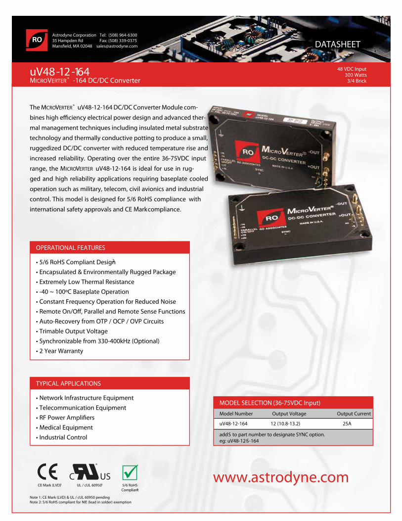
www.astrodyne.com
Astrodyne Corporation Tel: (508) 964-630035 Hampden Rd Fax: (508) 339-0375Manseld, MA 02048 [email protected]
The MICROVERTER® uV48-12-164 DC/DC Converter Module com-
bines high eciency electrical power design and advanced ther-
mal management techniques including insulated metal substrate
technology and thermally conductive potting to produce a small,
ruggedized DC/DC converter with reduced temperature rise and
increased reliability. Operating over the entire 36-75VDC input
range, the MICROVERTER uV48-12-164 is ideal for use in rug-
ged and high reliability applications requiring baseplate cooled
operation such as military, telecom, civil avionics and industrial
control. This model is designed for 5/6 RoHS compliance with
international safety approvals and CE Mark1 compliance.
OPERATIONAL FEATURES
• 5/6 RoHS Compliant Design2
• Encapsulated & Environmentally Rugged Package• Extremely Low Thermal Resistance• -40 ~ 100ºC Baseplate Operation• Constant Frequency Operation for Reduced Noise• Remote On/O¢, Parallel and Remote Sense Functions• Auto-Recovery from OTP / OCP / OVP Circuits• Trimable Output Voltage• Synchronizable from 330-400kHz (Optional)• 2 Year Warranty
TYPICAL APPLICATIONS
• Network Infrastructure Equipment• Telecommunication Equipment• RF Power Ampliers• Medical Equipment• Industrial Control
uV48-12-164MICROVERTER ® -164 DC/DC Converter
48 VDC Input300 Watts
3/4 Brick
MODEL SELECTION (36-75VDC Input)
Model Number Output Voltage Output Current
uV48-12-164 12 (10.8-13.2) 25A
add S to part number to designate SYNC option.eg: uV48-12-S-164
Note 1: CE Mark (LVD) & UL / cUL 60950 pending Note 2: 5/6 RoHS compliant for NIE (lead in solder) exemption
CE Mark (LVD)1 UL / cUL 609501 5/6 RoHSCompliant2
C US®
DATASHEET

www.astrodyne.comTel: (508) 964-6300
Fax: (508) [email protected]
Astrodyne Corporation35 Hampden RoadManseld, MA 02048
uV48-12-164 48 VDC Input / 300 Watts / 3/4 Brick
ABSOLUTE MAXIMUM RATINGS Exceeding absolute maximum ratings may cause permanent damage or reduce reliability
snoitidnoCstinUmumixaMmuminiMretemaraP
suounitnoCCDV 083.0-)nI- ot nI+( egatloV tupnI
Transient Input Voltage (+In to -In -0.3 100 VDC 100 msec. Max.
Parallel Pin Voltage (Parallel-On/O Pin to -In) -0.3 6.0 VDC
CDV 0002egatloV tuptuO-ot-tupnI
CDV 0051egatoV esaC-ot-tupnI
CDV 005egatloV esaC-ot-tuptuO
Cº011+04-erutarepmeT egarotS
etalpesaBCº001+04-erutarepmeT gnitarepO
.ces 5 <Cº062)redloS evaW( erutarepmeT gniredloS
ELECTRICAL SPECIFICATIONS Electrical specications apply for Vin=48VDC, Vout=12VDC, Full Load, Tc=25ºC unless specied otherwise
snoitidnoCstinUmumixaMlacipyTmuminiMtupnI
CDV578463egatloV tupnI
V63=niV ,Cº52=cTCDA8.9tnerruC tupnI mumixaM
10.0 ADC Tc=100ºC, Vin=36V
zH021=fBd06noitcejeR elppiR tupnIsnoitidnoCstinUmumixaMlacipyTmuminiMtuptuO
Voltage Set Point 11.88 12.01 12.12 VDC
daoL lluF ot 0%2.050.0noitalugeR daoL
xam niV ot nim niV%2.050.0noitalugeR eniL
xam cT ot nim cTCº / %20.0erutarepmeT/w tfirD egatloV
Cº52=cT ,V84=niVp-p Vm042021)DRAP( elppiR
360 mV p-p 36V<Vin<75V, -40ºC<Tc<+100ºC
A52tnerruC detaR
Overcurrent Inception Point 105 115 130 % Rated Vout=95% of Vout nominal
detaR %071tnerruC tiucriC trohS 36V<Vin<75V,Rshort=15mOhm
/A5.0 ,tnerruC detaR %08-02Vm004noitaiveD esnopseR tneisnarT µs
Transient Response Settling Time 250 µs 20-80% Rated Current, 0.5A/µs
detaR %57=tuoI ,V84=niV%5.88ycneiciffE
057ecnaticapaC daoL lanretxE µFsnoitidnoCstinUmumixaMlacipyTmuminiMnoitalosI
deriuqeR dohteM tseT laicepSCDV0002noitalosI tuptuO-ot-tupnI
CDV0051noitalosI esaC-ot-tupnI
CDV005noitalosI esaC-ot-tuptuO
Fp0522ecnaticapaC tuptuO-ot-tupnI
V005mhO M01ecnatsiseR tuptuO-ot-tupnI
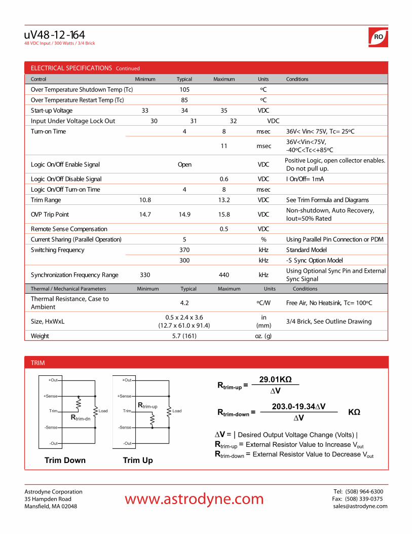
www.astrodyne.comTel: (508) 964-6300
Fax: (508) [email protected]
Astrodyne Corporation35 Hampden RoadManseld, MA 02048
uV48-12-164 48 VDC Input / 300 Watts / 3/4 Brick
TRIM
ELECTRICAL SPECIFICATIONS Continued
snoitidnoCstinUmumixaMlacipyTmuminiMlortnoC
Over Temperature Shutdown Temp (Tc) Cº501
Over Temperature Restart Temp (Tc) Cº58
CDV534333egatloV pu-tratS
Input Under Voltage Lock Out 30 31 32 VDC
Cº52=cT ,V57<niV<V63cesm84emiT no-nruT
11 msec 36V<Vin<75V,-40ºC<Tc<+85ºC
CDVnepOlangiS elbanE ffO/nO cigoLPositive Logic, open collector enables. Do not pull up.
Am1=ffO/nO ICDV6.0langiS elbasiD ffO/nO cigoL
cesm84emiT no-nruT ffO/nO cigoL
smargaiD dna alumroF mirT eeSCDV2.318.01egnaR mirT
CDV8.519.417.41tnioP pirT PVO Non-shutdown, Auto Recovery, Iout=50% Rated
CDV5.0noitasnepmoC esneS etomeR
MDP ro noitcennoC niP lellaraP gnisU%5)noitarepO lellaraP( gnirahS tnerruC
ledoM dradnatSzHk073ycneuqerF gnihctiwS
ledoM noitpO cnyS S-zHk003
zHk044033egnaR ycneuqerF noitazinorhcnyS Using Optional Sync Pin and External Sync Signal
Thermal / Mechanical Parameters Minimum Typical Maximum Units Conditions
Thermal Resistance, Case to Ambient Cº001=cT ,knistaeH oN ,riA eerFW/Cº2.4
Size, HxWxL 0.5 x 2.4 x 3.6(12.7 x 61.0 x 91.4)
in(mm) 3/4 Brick, See Outline Drawing
)g( .zo)161( 7.5thgieW
∆V = | Desired Output Voltage Change (Volts) |Rtrim-up = External Resistor Value to Increase Vout
Rtrim-down = External Resistor Value to Decrease Vout
Rtrim-up =29.01KΩ
∆V
Rtrim-down =203.0-19.34∆V
KΩ∆VRtrim-dn
+Out
+Sense
Trim
-Sense
-Out
LoadRtrim-up
+Out
+Sense
Trim
-Sense
-Out
Load
Trim Down Trim Up

www.astrodyne.comTel: (508) 964-6300
Fax: (508) [email protected]
Astrodyne Corporation35 Hampden RoadManseld, MA 02048
uV48-12-164 48 VDC Input / 300 Watts / 3/4 Brick
LOSSES VS. LOAD, Vin=48V
Loss
es (W
)
Output Current (A)
OUTPUT CHARACTERISTIC, Vin=48V, TC=25ºC
EFFICIENCY VS. LOAD, Vin=48V
TRANSIENT RESPONSE, Vin=48V, Iout=5A-20A-5A, Tc=25ºC
OUTPUT RIPPLE, Vin=48V, Iout=25A, Tc=25ºC
Eci
ency
(%)
Output Current (A)
Out
put V
olta
ge (V
)
Output Current (% of Full Load)
lout
, 5A
/div
. V
out,
0.5/
div.
t, 100 µs/div. 30MHz BW Current Slew Rate 0.5A/ µs
65
70
75
80
85
90
0 5 10 15 20 25
TC = 25 °CTC = 100 °C
INPUT CHARACTERISTIC, Iout=25A, TC=25ºC
Inpu
t Cur
rent
(A)
Input Voltage (V)
12
10
8
6
4
2
00 20 40 60 80 100 120 140
30MHz BW t, 1 µs/div.
50m
V pe
r div
.
0
5
10
15
20
25
30
35
40
45
50
0 5 10 15 20 25
TC = 25 °CTC =100 °C
0
321
456789
101112
0 5 10 15 20 25 30 35 40 45 50 55 60 65 70 75

www.astrodyne.comTel: (508) 964-6300
Fax: (508) [email protected]
Astrodyne Corporation35 Hampden RoadManseld, MA 02048
uV48-12-164 48 VDC Input / 300 Watts / 3/4 Brick
OUTLINE DRAWING Dimesions in Inches
NOTES
revA
KNISTAEH MUNIMULAECAFRUS
52.0
*
79DSEJ ,lekcin revo dlog si hsinif niP.4e yrogetac tcennocretni level dn2
.noitpo cnys gniredro nehw secalp 01.nwohs nip cnys lanoitpo fo noitacoL
.NIM 02.0
*
:ETON
02.0
80.0
21.051.0
21.051.0
04.246.1
EDIS NIPEDIS RAEN
NIP .AID 040.0YOLLA SSARB
SECALP 9
03.1
*
03.3
FFO/NO-LELLARAP
NI+NI+
NI-NI-
*CNYS
02.002.306.3
NIP .AID 731.0 YTIVITCUDNOC HGIH
YOLLA REPPOCSECALP 2
05.0
PEED 91.0 X .AID 82.0SECALP 4
00.2
URHT.AID 341.0SECALP 4
TUO-
MIRT
TUO+
S-
S+C/N 51.0
51.0
02.0
05.0
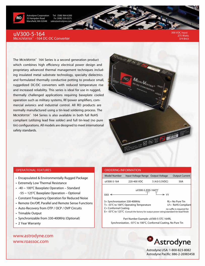
Astrodyne Corporation Tel: (508) 964-630035 Hampden Road Fx: (508) 339-0375
300 VDC Input275 Watts
3/4 BrickuV300-5-164MICROVERTER ® -164 DC-DC Converter
The MICROVERTER® 164 Series is a second generation product
proprietary advanced thermal management techniques includ-ing insulated metal substrate technology, specialty dielectrics and formulated thermally conductive potting to produce small, ruggedized DC/DC converters with reduced temperature rise and increased reliability. This series is ideal for use in rugged, thermally challenged applications requiring baseplate cooled
mercial avionics and industrial control. All RO products are normally manufactured using a tin-lead soldering process. The MICROVERTER® 164 Series is also available in both full RoHS compliant (utilizing lead free solder) and full tin-lead (no pure
safety standards.
OPERATIONAL FEATURES
• Encapsulated & Environmentally Rugged Package• Extremely Low Thermal Resistance• -40 ~ 100°C Baseplate Operation – Standard -55 ~ 125°C Baseplate Operation – Optional• Constant Frequency Operation for Reduced Noise•• Auto-Recovery from OTP / OCP / OVP Circuits• Trimable Output• Synchronizable from 330-400KHz (Optional)• 2 Year Warranty
XXX YY
S= Synchronization 330-400KHz RL= No Pure TinT= -55°C to 100°C Operating Temperature LF= RoHS CompliantC= Conformal Coating E= -55°C to 125°C (Consult the factory for output power rating)
Part Number Example: uV300-5-STC-164RLSynchronization, -55°C to 100°C, Conformal Coating, No Pure Tin
uV300-5-XXX-164YY
ORDERING INFORMATION Model Number Input Voltage Range Output Voltage Output Current
uV300-5-164 220-400 VDC 5 (4.0-5.5VDC) 50A
www.astrodyne.comwww.roassoc.com
Astrodyne USA: 1-800-823-8082

uV300-5-164 300 VDC Input / 275 Watts / 3/4 Brick
ABSOLUTE MAXIMUM RATINGS Exceeding absolute maximum ratings may cause permanent damage or reduce reliability
snoitidnoCstinUmumixaMmuminiMnoitpOretemaraP
suounitnoCCDV 0043.0-)nI- ot nI+( egatloV tupnI
Transient Input Voltage (+In to -In) -0.3 450 VDC 100 msec. Max.
CDV 0054noitalosI tuptuO/tupnI
CDV 0052noitalosI esaC/tupnI
CDV 005noitalosI esaC/tuptuO
Storage Temperature Standard -40 +110 ºC
T -55 +110 °C
E -55 +130 °C
Operating Temperature Standard -40 +110 ºC Baseplate
T -55 +100 °C Baseplate
E -55 +125 °C Baseplate
Soldering Temperature (Wave Solder) 260 ºC < 5 sec.
ELECTRICAL SPECIFICATIONS Electrical specications apply for Vin=300VDC, Vout=5VDC, Full Load, Tc=25ºC unless specied otherwise
snoitidnoCstinUmumixaMlacipyTmuminiMtupnI
CDV004003022egatloV tupnI
Cº52=cT ,V022=niVCDA4.1tnerruC tupnI mumixaM
1.5 ADC Vin=220V, Tc=100ºCp-p V51=elppir niV ,zH021=fBd07noitcejeR elppiR tupnI
snoitidnoCstinUmumixaMlacipyTmuminiMtuptuO
Voltage Set Point 4.95 5.00 5.05 VDC
daoL lluF ot 0%2.050.0noitalugeR daoL
xam niV ot nim niV%2.050.0noitalugeR eniL
xam cT ot nim cTCº / %20.0erutarepmeT/w tfirD egatloV
Cº52=cT ,V003=niVp-p Vm00106)DRAP( elppiR
150 mV p-p 220V<Vin<400V, -40ºC<Tc<+100ºC
A05tnerruC detaR
Overcurrent Inception Point 105 115 130 % Rated Vout=95% Vout nominal
mhom 51=trohsR ,V004<niV<V022detaR %071tnerruC tiucriC trohS
sµ/A5.0 ,tnerruC detaR %08-02Vm001noitaiveD esnopseR tneisnarT
V%1± ,sµ/A5.0 ,tnerruC detaR %08-02sµ001emiT gniltteS esnopseR tneisnarT o
detaR %57=tuoI ,V003=niV%28ycneiciffEsnoitidnoCstinUmumixaMlacipyTmuminiMnoitalosI
deriuqeR dohteM tseT laicepSCDV0054tuptuO-ot-tupnI
CDV0052esaC-ot-tupnI
CDV005esaC-ot-tuptuO
Fp0065ecnaticapaC tuptuO-ot-tupnI
V005mhO M01ecnatsiseR tuptuO-ot-tupnI
www.astrodyne.comwww.roassoc.com
Astrodyne USA: 1-800-823-8082Astrodyne Pacic: 886-2-26983458
uV300-5-164 300 VDC Input / 275 Watts / 3/4 Brick
ELECTRICAL SPECIFICATIONS Continued
snoitidnoCstinUmumixaMlacipyTmuminiMnoitpOlortnoC
Over Temperature Shutdown Temp (Tc) Standard & T 105 ºCE 130 °C
Over Temperature Restart Temp (Tc) Standard & T 85 ºC
E 105 °CCDV002571egatloV pu-tratS
CDV031tuO kcoL egatloV rednU tupnI
Cº52=cT ,V004<niV<022cesm0381emiT no-nruT
40 msec 220<Vin<400V,-40ºC<Tc<+100ºC
CDVnepOlangiS elbanE ffO/nO cigoL Positive Logic, open collector enables. Do not pull up.
Am1=ffO/nO ICDV6.0langiS elbasiD ffO/nO cigoL
cesm015emiT no-nruT ffO/nO cigoL
smargaiD dna alumroF mirT eeSCDV5.54egnaR mirT
CDV6.62.69.5tnioP pirT PVO Non-shutdown, Auto Recovery, Iout=50% Rated
detimil PVO eb yaMCDV5.0noitasnepmoC esneS etomeR
MDP ro noitcennoC niP lellaraP gnisU%5)noitarepO lellaraP( gnirahS tnerruC
ledoM dradnatSzHK073ycneuqerF gnihctiwS
300 KHz -S Sync Option Model
zHK044033egnaR ycneuqerF gnihctiwS Using Optional Sync Pin and External Sync Signal
Thermal / Mechanical Parameters Option Minimum Typical Maximum Units Conditions
Cº001=cT ,knistaeH oN ,riA eerFW/Cº2.4tneibmA ot esaC ,ecnatsiseR lamrehT
Size, HxWxL 0.5 x 2.4 x 3.6(12.7 x 61.0 x 91.4)
in(mm) 3/4 Brick, See Outline Drawing
)g( .zo)161( 7.5thgieW
TRIM
Rtrim-dn
+Out
+Sense
Trim
-Sense
-Out
LoadRtrim-up
+Out
+Sense
Trim
-Sense
-Out
Load
∆ V = | Desired Output Voltage Change (Volts) |R trim-up = External Resistor Value to Increase V out
Rtrim-down = External Resistor Value to Decrease V out
R trim-up =8.516K Ω
∆ V
Trim Down Trim Up
R trim-down =19.87 - 5.677 ∆ V
K Ω∆ V
www.astrodyne.comwww.roassoc.com
Astrodyne USA: 1-800-823-8082Astrodyne Pacic: 886-2-26983458

EFFICIENCY VS. LOAD, Vin=300V, TC=25ºC
uV300-5-164 300 VDC Input / 275 Watts / 3/4 Brick
INPUT CHARACTERISTIC, Vin=300V, TC=25ºC
LOSSES VS. LOAD, Vin=300V, TC=25ºC
OUTPUT RIPPLE, Vin=300V, Iout=50A, Tc=25ºC
OUTPUT CHARACTERISTIC, Vin=300V, TC=25ºC
TRANSIENT RESPONSE, Vin=300V, Iout=10A-40A-10A, Tc=25ºC
50mVperdiv.
Inpu
t Cur
rent
(A)
Out
put V
olta
ge (V
)
Loss
es (W
)
lout
, 10A
/div
.
vou
t, 10
0mV/
div.
65
70
75
80
85
90
0 10 20 30 40 50
05
101520253035404550556065
0 10 20 30 40 50
0.0
0.5
1.0
1.5
2.0
0 50 100 150 200 250 300 350 4000.0
1.0
2.0
3.0
4.0
5.0
6.0
0 20 40 60 80 100 120 140 160
www.astrodyne.comwww.roassoc.com
Astrodyne USA: 1-800-823-8082
Output Current (A) t 1µs/div. 30MHz BWL
Output Current (A)
Input Voltage (V) Output Current (% of Full Load)
t 1µs/div. 30MHz BWL Current Slew Rate .05A/ µs

uV300-5-164 300 VDC Input / 275 Watts / 3/4 Brick
OUTLINE DRAWING Dimensions in Inches
NOTES
2.40
0.28 DIA. X 0.19 DEEP4 PLACES
0.50
0.040 DIA. PIN BRASS ALLOY7 PLACES
0.20 MIN.
NOTE:Pin finish is gold over nickel, JESD972nd level interconnect category e4.
* 8 places when ordering sync option.Location of optional sync pin shown.
1.300.08
ALUMINUM HEATSINKSURFACE
0.25
* *
3.30
PARALLEL-ON/OFF-IN
+IN0.270.15
1.64
0.20
0.20
-S
+S+OUT
-OUT
N/C TRIM
PIN SIDENEAR SIDE
SYNC*
3.203.60
0.137 DIA. PINHIGH CONDUCTIVITY COPPER ALLOY2 PLACES
0.143 DIA.THRU4 PLACES
0.50 2.000.200.150.15
REV 090410
www.astrodyne.comwww.roassoc.com
Astrodyne USA: 1-800-823-8082Astrodyne Pacic: 886-2-26983458

300 VDC Input288 Watts
3/4 BrickuV300-8-164MICROVERTER ® -164 DC-DC Converter
The MICROVERTER® 164 Series is a second generation product which combines high eciency electrical power design and proprietary advanced thermal management techniques includ-ing insulated metal substrate technology, specialty dielectrics and formulated thermally conductive potting to produce small, ruggedized DC/DC converters with reduced temperature rise and increased reliability. This series is ideal for use in rugged, thermally challenged applications requiring baseplate cooled operation such as military systems, RF/power ampliers, com-mercial avionics and industrial control. All RO products are normally manufactured using a tin-lead soldering process. The MICROVERTER 164 Series is also available in both full RoHS compliant (utilizing lead free solder) and full tin-lead (no pure tin) congurations. All models are designed to meet international safety standards.
MADE IN U.S.A.
OPERATIONAL FEATURES
• Encapsulated & Environmentally Rugged Package• Extremely Low Thermal Resistance• -40 ~ 100°C Baseplate Operation – Standard -55 ~ 125°C Baseplate Operation – Optional• Constant Frequency Operation for Reduced Noise• Remote On/O, Parallel and Remote Sense Functions• Auto-Recovery from OTP / OCP / OVP Circuits• Trimable Output• Synchronizable from 330-400KHz (Optional)• 2 Year Warranty
XXX YY
S= Synchronization 330-400KHz RL= No Pure TinT= -55°C to 100°C Operating Temperature LF= RoHS CompliantC= Conformal Coating E= -55°C to 125°C (Consult the factory for output power rating)
Part Number Example: uV300-8-STC-164RLSynchronization, -55°C to 100°C, Conformal Coating, No Pure Tin
uV300-8-XXX-164YY
no sux is required for standard tin-lead nish
ORDERING INFORMATION Model Number Input Voltage Range Output Voltage Output Current
uV300-8-164 220-400 VDC 8 (6.4-8.8VDC) 36A
www.astrodyne.comwww.roassoc.com
Astrodyne USA: 1-800-823-8082
Astrodyne Corporation Tel: (508) 964-630035 Hampden Road Fx: (508) 339-0375
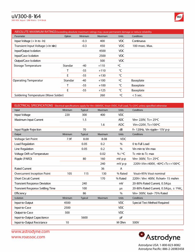
uV300-8-164 300 VDC Input / 288 Watts / 3/4 Brick
ABSOLUTE MAXIMUM RATINGS Exceeding absolute maximum ratings may cause permanent damage or reduce reliability
snoitidnoCstinUmumixaMmuminiMnoitpOretemaraP
suounitnoCCDV 0043.0-)nI- ot nI+( egatloV tupnI
Transient Input Voltage (+In to -In) -0.3 450 VDC 100 msec. Max.
CDV 0054noitalosI tuptuO/tupnI
CDV 0052noitalosI esaC/tupnI
CDV 005noitalosI esaC/tuptuO
Storage Temperature Standar -40 +110 ºC
T -55 +110 °C
E -55 +130 °C
Operating Temperatur Standar -40 +100 ºC Baseplate
T -55 +100 °C Baseplate
E -55 +125 °C Baseplate
Soldering Temperature (Wave Solder) 260 ºC < 5 sec.
ELECTRICAL SPECIFICATIONS Electrical specications apply for Vin=300VDC, Vout=5VDC, Full Load, Tc=25ºC unless specied otherwise
snoitidnoCstinUmumixaMlacipyTmuminiMtupnI
CDV004003022egatloV tupnI
Cº52=cT ,V022=niVCDA5.1tnerruC tupnI mumixaM
1.6 ADC Vin=220V, Tc=100ºC
p-p V51=elppir niV ,zH021=fBd07noitcejeR elppiR tupnIsnoitidnoCstinUmumixaMlacipyTmuminiMtuptuO
Voltage Set Point 7.9f 8.00 8.08 VDC
daoL lluF ot 0%2.050.0noitalugeR daoL
xam niV ot nim niV%2.050.0noitalugeR eniL
xam cT ot nim cTCº / %20.0erutarepmeT/w tfirD egatloV
Cº52=cT ,V003=niVp-p Vm06108)DRAP( elppiR
240 mV p-p 220V<Vin<400V, -40ºC<Tc<+100ºC
A63tnerruC detaR
Overcurrent Inception Point 105 115 130 % Rated Vout=95% Vout nominal
mhom 51=trohsR ,V004<niV<V022detaR %071tnerruC tiucriC trohS
sµ/A5.0 ,tnerruC detaR %08-02Vm042noitaiveD esnopseR tneisnarT
V%1± ,sµ/A5.0 ,tnerruC detaR %08-02sµ001emiT gniltteS esnopseR tneisnarT o
detaR %57=tuoI ,V003=niV%68ycneiciffEsnoitidnoCstinUmumixaMlacipyTmuminiMnoitalosI
deriuqeR dohteM tseT laicepSCDV0054tuptuO-ot-tupnI
CDV0052esaC-ot-tupnI
CDV005esaC-ot-tuptuO
Fp0065ecnaticapaC tuptuO-ot-tupnI
V005mhO M01ecnatsiseR tuptuO-ot-tupnI
www.astrodyne.comwww.roassoc.com
Astrodyne USA: 1-800-823-8082

uV300-8-164 300 VDC Input / 288 Watts / 3/4 Brick
ELECTRICAL SPECIFICATIONS Continued
snoitidnoCstinUmumixaMlacipyTmuminiMnoitpOlortnoC
Over Temperature Shutdown Temp (Tc) Standard & T 105 ºC
E 130 °C
Over Temperature Restart Temp (Tc) Standard & T 85 ºC
E 105 °C
CDV002571egatloV pu-tratS
CDV031tuO kcoL egatloV rednU tupnI
Cº52=cT ,V004<niV<022cesm0381emiT no-nruT
40 msec 220<Vin<400V,-40ºC<Tc<+100ºC
CDVnepOlangiS elbanE ffO/nO cigoL Positive Logic, open collector enables. Do not pull up.
Am1=ffO/nO ICDV6.0langiS elbasiD ffO/nO cigoL
cesm015emiT no-nruT ffO/nO cigoL
smargaiD dna alumroF mirT eeSCDV8.86.4egnaR mirT
CDV10.46.92.9tnioP pirT PVO Non-shutdown, Auto Recovery, Iout=50% Rated
detimil PVO eb yaMCDV5.0noitasnepmoC esneS etomeR
MDP ro noitcennoC niP lellaraP gnisU%5)noitarepO lellaraP( gnirahS tnerruC
ledoM dradnatSzHK073ycneuqerF gnihctiwS
300 KHz -S Sync Option Model
zHK044033egnaR ycneuqerF gnihctiwSUsing Optional Sync Pin and External Sync Signal
Thermal / Mechanical Parameters Option Minimum Typical Maximum Units Conditions
Cº001=cT ,knistaeH oN ,riA eerFW/Cº2.4tneibmA ot esaC ,ecnatsiseR lamrehT
Size, HxWxL 0.5 x 2.4 x 3.6(12.7 x 61.0 x 91.4)
in(mm) 3/4 Brick, See Outline Drawing
)g( .zo)161( 7.5thgieW
TRIM
Rtrim-dn
+Out
+Sense
Trim
-Sense
-Out
LoadRtrim-up
+Out
+Sense
Trim
-Sense
-Out
Load
∆ V = | Desired Output Voltage Change (Volts) |R trim-up = External Resistor Value to Increase Vout
R trim-down = External Resistor Value to Decrease Vout
R trim-up =15.84K Ω
∆ V
Trim Down Trim Up
R trim-down =68.67- 10.56 ∆ V
K Ω∆ V
www.astrodyne.comwww.roassoc.com
Astrodyne USA: 1-800-823-8082
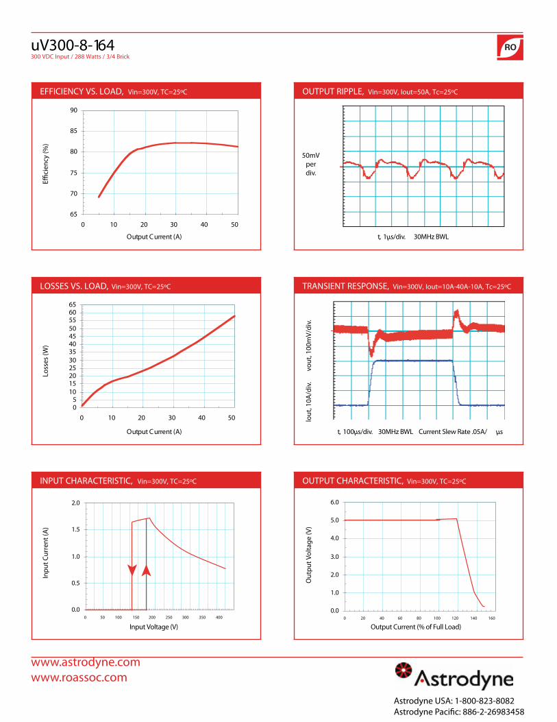
EFFICIENCY VS. LOAD, Vin=300V, TC=25ºC
uV300-8-164 300 VDC Input / 288 Watts / 3/4 Brick
INPUT CHARACTERISTIC, Vin=300V, TC=25ºC
LOSSES VS. LOAD, Vin=300V, TC=25ºC
OUTPUT RIPPLE, Vin=300V, Iout=50A, Tc=25ºC
OUTPUT CHARACTERISTIC, Vin=300V, TC=25ºC
TRANSIENT RESPONSE, Vin=300V, Iout=10A-40A-10A, Tc=25ºC
Eci
ency
(%)
50mVperdiv.
1 ,t)A( tnerruC tuptuO µs/div. 30MHz BWL
Inpu
t Cur
rent
(A)
Input Voltage (V)
Out
put V
olta
ge (V
)
Output Current (% of Full Load)
Loss
es (W
)
lout
, 10A
/div
.
vou
t, 10
0mV/
div.
001 ,t)A( tnerruC tuptuO µs/div. 30MHz BWL Current Slew Rate .05A/ µs
65
70
75
80
85
90
0 10 20 30 40 50
05
101520253035404550556065
0 10 20 30 40 50
0.0
0.5
1.0
1.5
2.0
0 50 100 150 200 250 300 350 4000.0
1.0
2.0
3.0
4.0
5.0
6.0
0 20 40 60 80 100 120 140 160
www.astrodyne.comwww.roassoc.com
Astrodyne USA: 1-800-823-8082
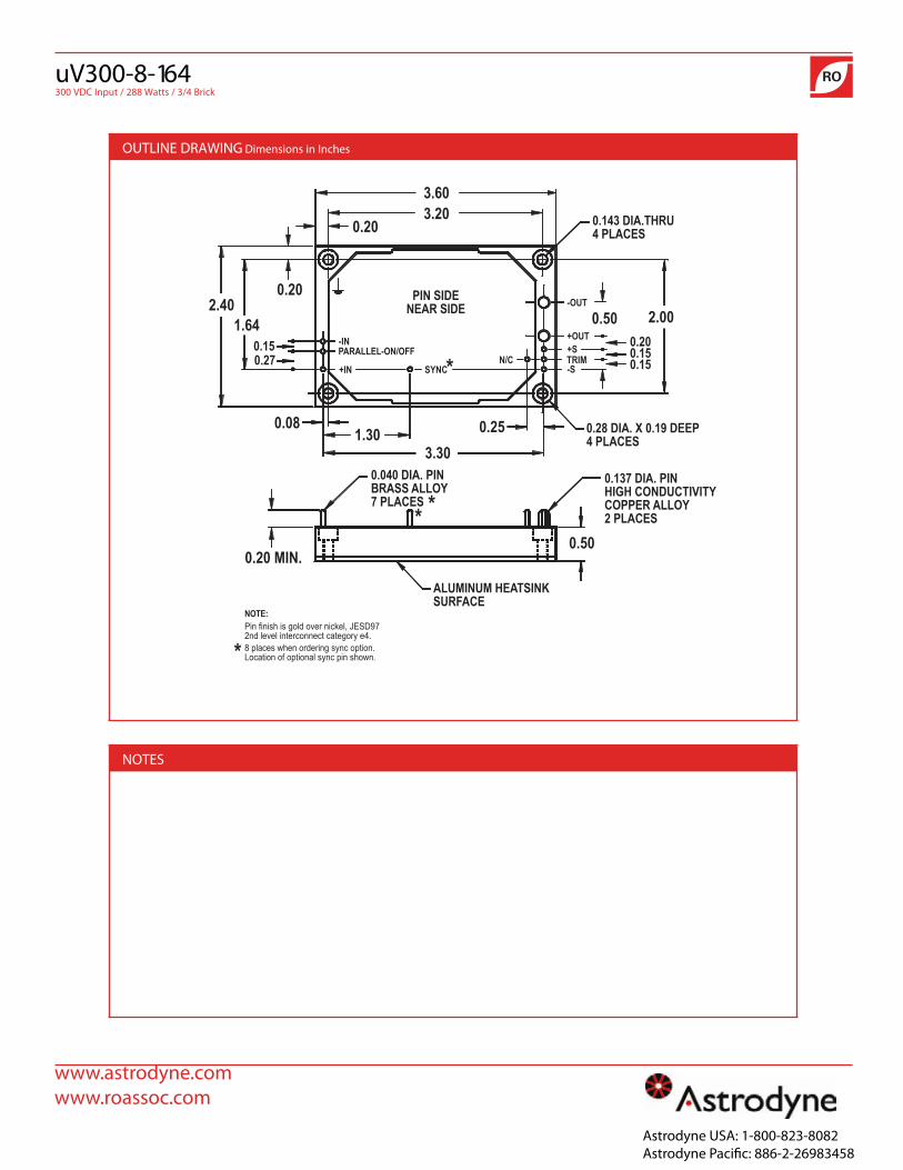
uV300-8-164 300 VDC Input / 288 Watts / 3/4 Brick
OUTLINE DRAWING Dimensions in Inches
NOTES
2.40
0.28 DIA. X 0.19 DEEP4 PLACES
0.50
0.040 DIA. PIN BRASS ALLOY7 PLACES
0.20 MIN.
NOTE:Pin finish is gold over nickel, JESD972nd level interconnect category e4.
* 8 places when ordering sync option.Location of optional sync pin shown.
1.300.08
ALUMINUM HEATSINKSURFACE
0.25
* *
3.30
PARALLEL-ON/OFF-IN
+IN0.270.15
1.64
0.20
0.20
-S
+S+OUT
-OUT
N/C TRIM
PIN SIDENEAR SIDE
SYNC*
3.203.60
0.137 DIA. PINHIGH CONDUCTIVITY COPPER ALLOY2 PLACES
0.143 DIA.THRU4 PLACES
0.50 2.000.200.150.15
www.astrodyne.comwww.roassoc.com
Astrodyne USA: 1-800-823-8082

RO
300 VDC Input300 Watts
3/4 Brick
The MICROVERTER® 164 Series is a second generation product which combines high eciency electrical power design and proprietary advanced thermal management techniques includ-ing insulated metal substrate technology, specialty dielectrics and formulated thermally conductive potting to produce small, ruggedized DC/DC converters with reduced temperature rise and increased reliability. This series is ideal for use in rugged, thermally challenged applications requiring baseplate cooled operation such as military systems, RF/power ampliers, com-mercial avionics and industrial control. All RO products are normally manufactured using a tin-lead soldering process. The MICROVERTER® 164 Series is also available in both full RoHS compliant (utilizing lead free solder) and full tin-lead (no pure tin) congurations. All models are designed to meet international safety standards.
uV300-12-164MICROVERTER ® -164 DC-DC Converter
OPERATIONAL FEATURES
• Encapsulated & Environmentally Rugged Package• Extremely Low Thermal Resistance• -40 ~ 100°C Baseplate Operation – Standard -55 ~ 125°C Baseplate Operation – Optional• Constant Frequency Operation for Reduced Noise• Remote On/O, Parallel and Remote Sense Functions• Auto-Recovery from OTP / OCP / OVP Circuits• Trimable Output• Synchronizable from 330-400KHz (Optional)• 2 Year Warranty
XXX YY
S= Synchronization 330-400KHz RL= No Pure TinT= -55°C to 100°C Operating Temperature LF= RoHS CompliantC= Conformal Coating E= -55°C to 125°C (Consult the factory for output power rating)
Part Number Example: uV300-12-STC-164RLSynchronization, -55°C to 100°C, Conformal Coating, No Pure Tin
uV300-12-XXX-164YY
no sux is required for standard tin-lead nish
ORDERING INFORMATION Model Number Input Voltage Range Output Voltage Output Current
uV300-12-164 220-400 VDC 12 (10.8-13.2 VDC) 25A
Astrodyne Corporation Tel: (508) 964-630035 Hampden Road Fx: (508) 339-0375Manseld, MA 02048 [email protected]
www.astrodyne.comwww.roassoc.com
Astrodyne USA: 1-800-823-8082Astrodyne Pacic: 886-2-26983458

uV300-12-164300 VDC Input / 300 Watts / 3/4 Brick
ABSOLUTE MAXIMUM RATINGS Exceeding absolute maximum ratings may cause permanent damage or reduce reliability
snoitidnoCstinUmumixaMmuminiMnoitpOretemaraP
suounitnoCCDV 0043.0-)nI- ot nI+( egatloV tupnI
Transient Input Voltage (+In to 3.0-)nI- 450 VDC 100 msec. Max.
CDV 0054noitalosI tuptuO/tupnI
CDV 0052noitalosI esaC/tupnI
CDV 005noitalosI esaC/tuptuOStorage Temperatur Standard -40 +110 ºC
T -55 +110 °C
E -55 +130 °C
Operating Temperature Standard -40 +100 ºC BaseplateT -55 +100 °C Baseplate
E -55 +125 °C Baseplate
Soldering Temperature (Wave Solder) 260 ºC < 5 sec.
ELECTRICAL SPECIFICATIONS Electrical specications apply for Vin=300VDC, Vout=12VDC, Full Load, Tc=25ºC unless specied otherwise
snoitidnoCstinUmumixaMlacipyTmuminiMtupnI
CDV004003022egatloV tupnI
Cº52=cT ,V022=niVCDA6.1tnerruC tupnI mumixaM
1.9 ADC Vin=220V, Tc=100ºC
p-p V51=elppir niV ,zH021=fBd07noitcejeR elppiR tupnI
snoitidnoCstinUmumixaMlacipyTmuminiMtuptuO
CDV 21.2110.2188.11tnioP teS egatloV
daoL lluF ot 0%2.050.0noitalugeR daoL
xam niV ot nim niV%2.050.0noitalugeR eniL
xam cT ot nim cTCº / %20.0erutarepmeT/w tfirD egatloV
Cº52=cT ,V003=niVp-p Vm042031)DRAP( elppiR
360 mV p-p 220V<Vin<400V, -40ºC<Tc<+100ºC
A52tnerruC detaR
Overcurrent Inception Point 105 115 130 % Rated Vout=95% of Vout nominal
detaR %071tnerruC tiucriC trohS 220V<Vin<400V,Rshort=15 mohm
/A5.0 ,tnerruC detaR %08-02Vm008noitaiveD esnopseR tneisnarT µs
002emiT gniltteS esnopseR tneisnarT µs 20-80% Rated Current, 0.5A/µs, ±1% V o
detaR %57=tuoI ,V003=niV%58ycneiciffE
snoitidnoCstinUmumixaMlacipyTmuminiMnoitalosI
deriuqeR dohteM tseT laicepSCDV0054tuptuO-ot-tupnI
CDV0052esaC-ot-tupnI
CDV005esaC-ot-tuptuO
Fp0065ecnaticapaC tuptuO-ot-tupnI
V005mhO M01ecnatsiseR tuptuO-ot-tupnI
www.astrodyne.comwww.roassoc.com
Astrodyne USA: 1-800-823-8082Astrodyne Pacic: 886-2-26983458

uV300-12-164300 VDC Input / 300 Watts / 3/4 Brick
TRIM
ELECTRICAL SPECIFICATIONS Continued
snoitidnoCstinUmumixaMlacipyTmuminiMnoitpOlortnoC
Over Temperature Shutdown Temp (Tc) Standard & T 105 ºC
E 130 °C
Over Temperature Restart Temp (Tc) Standard & T 85 ºC
E 105 °C
CDV002571egatloV pu-tratS
CDV031tuO kcoL egatloV rednU tupnI
Cº52=cT ,V004<niV<022cesm0381emiT no-nruT
40 msec 220<Vin<400V,-40ºC<Tc<+100ºC
CDVnepOlangiS elbanE ffO/nO cigoL Positive Logic, open collector enables. Do not pull up.
Am1=ffO/nO ICDV6.0langiS elbasiD ffO/nO cigoL
cesm015emiT no-nruT ffO/nO cigoL
smargaiD dna alumroF mirT eeSCDV2.318.01egnaR mirT
CDV8.519.417.41tnioP pirT PVO Non-shutdown, Auto Recovery, Iout=50% Rated
CDV5.0noitasnepmoC esneS etomeR
MDP ro noitcennoC niP lellaraP gnisU%5)noitarepO lellaraP( gnirahS tnerruC
ledoM dradnatSzHK073ycneuqerF gnihctiwS
300 KHz -S Sync Option Model
zHK044033egnaR ycneuqerF gnihctiwSUsing Optional Sync Pin and External Sync Signal
snoitidnoCstinUmumixaMlacipyTmuminiMsretemaraP lacinahceM / lamrehT
Thermal Resistance, Case to Ambient 4.2 ºC/W Free Air, No Heatsink, Tc=100ºC
Size, HxWxL 0.5 x 2.4 x 3.6(12.7 x 61.0 x 91.4)
in(mm) 3/4 Brick, See Outline Drawing
)g( .zo)161( 7.5thgieW
Rtrim-dn
+Out
+Sense
Trim
-Sense
-Out
LoadRtrim-up
+Out
+Sense
Trim
-Sense
-Out
Load
∆ V = | Desired Output Voltage Change (Volts) |R trim-up = External Resistor Value to Increase V out
R trim-down = External Resistor Value to Decrease V out
R trim-up =29.01K Ω
∆ V
Trim Down Trim Up
R trim-down =203.0-19.34 ∆ V
K Ω∆ V
www.astrodyne.comwww.roassoc.com
Astrodyne USA: 1-800-823-8082Astrodyne Pacic: 886-2-26983458
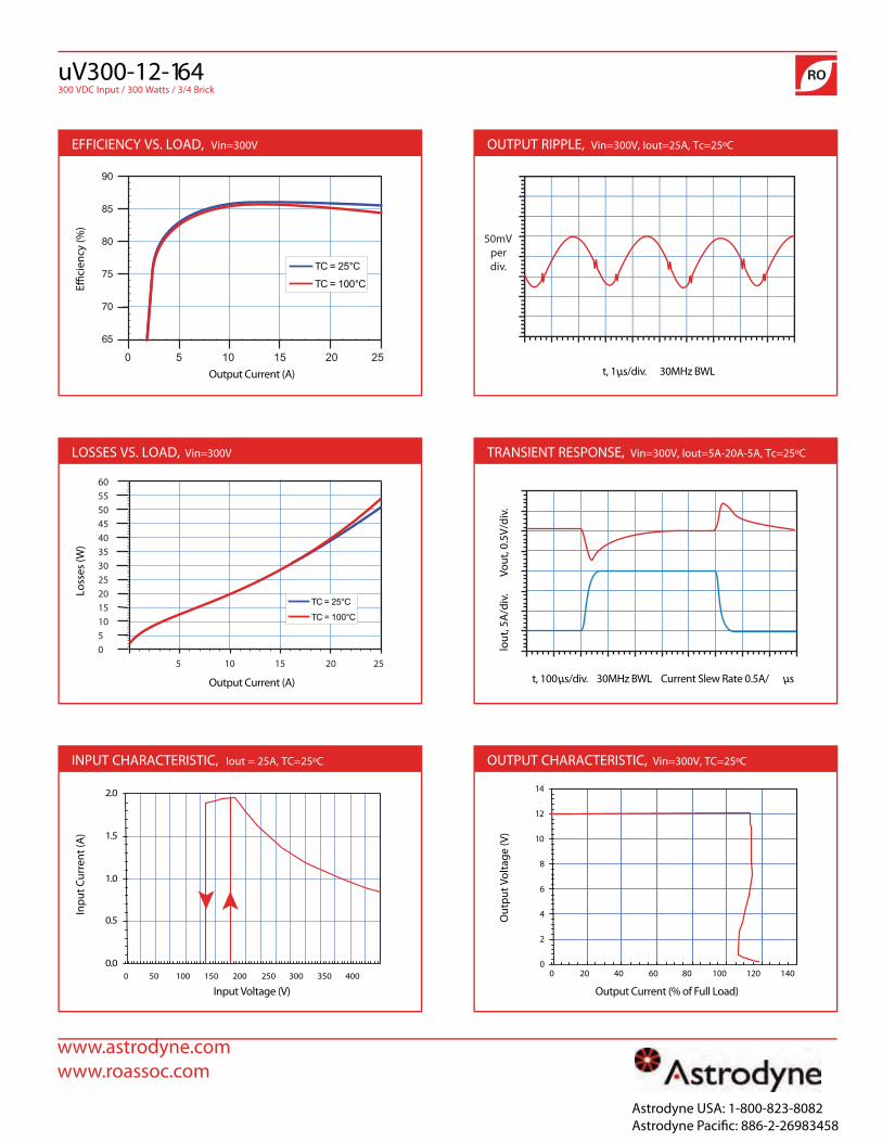
uV300-12-164300 VDC Input / 300 Watts / 3/4 Brick
EFFICIENCY VS. LOAD, Vin=300V
INPUT CHARACTERISTIC, Iout = 25A, TC=25ºC
LOSSES VS. LOAD, Vin=300V
OUTPUT RIPPLE, Vin=300V, Iout=25A, Tc=25ºC
OUTPUT CHARACTERISTIC, Vin=300V, TC=25ºC
TRANSIENT RESPONSE, Vin=300V, Iout=5A-20A-5A, Tc=25ºC
Eci
ency
(%)
Output Current (A)
Inpu
t Cur
rent
(A)
Input Voltage (V)
Out
put V
olta
ge (V
)
Output Current (% of Full Load)
Loss
es (W
)
lout
, 5A
/div
.
Vou
t, 0.
5V/d
iv.
Output Current (A) t, 100µs/div. 30MHz BWL Current Slew Rate 0.5A/ µs
0 5 10 15 20 25
0.0
0.5
1.0
1.5
2.0
0 50 100 150 200 250 300 350 400
50mVperdiv.
t, 1µs/div. 30MHz BWL
0
2
4
6
8
10
12
14
0 20 40 60 80 100 120 140
www.astrodyne.comwww.roassoc.com
Astrodyne USA: 1-800-823-8082Astrodyne Pacic: 886-2-26983458

uV300-12-164300 VDC Input / 300 Watts / 3/4 Brick
OUTLINE DRAWING Dimensions in Inches
NOTES
REV 090410
2.40
0.28 DIA. X 0.19 DEEP4 PLACES
0.50
0.040 DIA. PIN BRASS ALLOY7 PLACES
0.20 MIN.
NOTE:Pin finish is gold over nickel, JESD972nd level interconnect category e4.
* 8 places when ordering sync option.Location of optional sync pin shown.
1.300.08
ALUMINUM HEATSINKSURFACE
0.25
* *
3.30
PARALLEL-ON/OFF-IN
+IN0.270.15
1.64
0.20
0.20
-S
+S+OUT
-OUT
N/C TRIM
PIN SIDENEAR SIDE
SYNC*
3.203.60
0.137 DIA. PINHIGH CONDUCTIVITY COPPER ALLOY2 PLACES
0.143 DIA.THRU4 PLACES
0.50 2.000.200.150.15
www.astrodyne.comwww.roassoc.com
Astrodyne USA: 1-800-823-8082Astrodyne Pacic: 886-2-26983458

300 VDC Input300 Watts
3/4 BrickuV300-15-164MICROVERTER ® -164 DC/DC Converter
The MICROVERTER® 164 Series is a second generation product which combines high electrical power design and proprietary advanced thermal management techniques includ-ing insulated metal substrate technology, specialty dielectrics and formulated thermally conductive potting to produce small, ruggedized DC/DC converters with reduced temperature rise and increased reliability. This series is ideal for use in rugged, thermally challenged applications requiring baseplate cooled operation such as military systems, RF/power com-mercial avionics and industrial control. All RO products are normally manufactured using a tin-lead soldering process. The MICROVERTER® 164 Series is also available in both full RoHS compliant (utilizing lead free solder) and full tin-lead (no pure tin) All models are designed to meet international safety standards.
OPERATIONAL FEATURES
• Encapsulated & Environmentally Rugged Package• Extremely Low Thermal Resistance• -40 ~ 100°C Baseplate Operation – Standard -55 ~ 125°C Baseplate Operation – Optional• Constant Frequency Operation for Reduced Noise• Remote Parallel and Remote Sense Functions• Auto-Recovery from OTP / OCP / OVP Circuits• Trimable Output• Synchronizable from 330-400KHz (Optional)• 2 Year Warranty
XXX YY
S= Synchronization 330-400KHz RL= No Pure TinT= -55°C to 100°C Operating Temperature LF= RoHS CompliantC= Conformal Coating E= -55°C to 125°C (Consult the factory for output power rating)
Part Number Example: uV300-15-STC-164RLSynchronization, -55 °C to 100°C, Conformal Coating, No Pure Tin
uV300-15-XXX-164YY
no is required for standard tin-lead
ORDERING INFORMATION
Model Number Input Voltage Range Output Voltage Output Current
uV300-15-164 220-400 VDC 15 (12-16.5 VDC) 20A
www.astrodyne.comwww.roassoc.com
Astrodyne USA: 1-800-823-8082
Astrodyne Corporation Tel: (508) 964-630035 Hampden Road Fx: (508) 339-0375

uV300-15-164 300 VDC Input / 300 Watts / 3/4 Brick
ELECTRICAL SPECIFICATIONS Electrical specications apply for Vin=300VDC, Vout=15VDC, Full Load, Tc=25ºC unless specied otherwise
snoitidnoCstinUmumixaMlacipyTmuminiMtupnI
CDV004003022egatloV tupnI
Maximum Input Current 1.56 1.64 ADC Vin=220V, Tc=25ºC
1.64 ADC Vin=220V, Tc=100ºC
p-p V51=elppir niV ,zH021=fBd07noitcejeR elppiR tupnI
snoitidnoCstinUmumixaMlacipyTmuminiMtuptuO
CDV 51.5100.5158.41tnioP teS egatloV
daoL lluF ot 0%2.050.0noitalugeR daoL
xam niV ot nim niV%2.050.0noitalugeR eniL
xam cT ot nim cTCº / %20.0erutarepmeT/w tfirD egatloV
Cº52=cT ,V003=niVp-p Vm003001)DRAP( elppiR
450 mV p-p 220V<Vin<400V, -40ºC<Tc<+100ºC
A02tnerruC detaR
Overcurrent Inception Point 105 115 130 % Rated Vout=95% Vout nominal
detaR %071tnerruC tiucriC trohS 220V<Vin<400V,Rshort=15 mohm
/A5.0 ,tnerruC detaR %08-02Vm008noitaiveD esnopseR tneisnarT µs
002emiT gniltteS esnopseR tneisnarT µs 20-80% Rated Current, 0.5A/µs, ±1%Vo
detaR %57=tuoI ,V003=niV%68ycneiciffE
snoitidnoCstinUmumixaMlacipyTmuminiMnoitalosI
deriuqeR dohteM tseT laicepSCDV0054tuptuO-ot-tupnI
CDV0052esaC-ot-tupnI
CDV005esaC-ot-tuptuO
Fp0065ecnaticapaC tuptuO-ot-tupnI
V005mhO M01ecnatsiseR tuptuO-ot-tupnI
ABSOLUTE MAXIMUM RATINGS Exceeding absolute maximum ratings may cause permanent damage or reduce reliability
snoitidnoCstinUmumixaMmuminiMnoitpOretemaraP
suounitnoCCDV 0043.0-)nI- ot nI+( egatloV tupnI
Transient Input Voltage (+In to -In) -0.3 450 VDC 100 msec. Max.
CDV 0054noitalosI tuptuO/tupnI
CDV 0052noitalosI esaC/tupnI
CDV 005noitalosI esaC/tuptuOStorage Temperature Standard -40 +110 ºC
T -55 +110 °C
E -55 +130 °C
Operating Temperature Standard -40 +100 ºC Baseplate
T -55 +100 °C Baseplate
E -55 +125 °C Baseplate
Soldering Temperature (Wave Solder) 260 ºC < 5 sec.
www.astrodyne.comwww.roassoc.com
Astrodyne USA: 1-800-823-8082Astrodyne Pacic: 886-2-26983458

uV300-15-164 300 VDC Input / 300 Watts / 3/4 Brick
TRIM
ELECTRICAL SPECIFICATIONS Continued
snoitidnoCstinUmumixaMlacipyTmuminiMnoitpOlortnoC
Over Temperature Shutdown Temp (Tc) Standard & T 105 ºC
E 130 °C
Over Temperature Restart Temp (Tc) Standard & T 85 ºC
E 105 °C
CDV002571egatloV pu-tratS
CDV031tuO kcoL egatloV rednU tupnI
Cº52=cT ,V004<niV<022cesm0381emiT no-nruT
40 msec 220<Vin<400V,-40ºC<Tc<+100ºC
CDVnepOlangiS elbanE ffO/nO cigoL Positive Logic, open collector enables. Do not pull up.
Am1=ffO/nO ICDV6.0langiS elbasiD ffO/nO cigoL
cesm015emiT no-nruT ffO/nO cigoL
smargaiD dna alumroF mirT eeSCDV5.6121egnaR mirT
CDV57.916.816.71tnioP pirT PVO Non-shutdown, Auto Recovery, Iout=50% Rated
CDV5.0noitasnepmoC esneS etomeR
MDP ro noitcennoC niP lellaraP gnisU%5)noitarepO lellaraP( gnirahS tnerruC
ledoM dradnatSzHK073ycneuqerF gnihctiwS
300 KHz -S Sync Option Model
zHK044033egnaR ycneuqerF gnihctiwS Using Optional Sync Pin and External Sync Signal
snoitidnoCstinUmumixaMlacipyTmuminiMsretemaraP lacinahceM / lamrehT
Cº001=cT ,knistaeH oN ,riA eerFW/Cº2.4tneibmA ot esaC ,ecnatsiseR lamrehT
Size, HxWxL 0.5 x 2.4 x 3.6(12.7 x 61.0 x 91.4)
in(mm) 3/4 Brick, See Outline Drawing
)g( .zo)161( 7.5thgieW
Rtrim-dn
+Out
+Sense
Trim
-Sense
-Out
LoadRtrim-up
+Out
+Sense
Trim
-Sense
-Out
Load
∆ V = | Desired Output Voltage Change (Volts) |R trim-up = External Resistor Value to Increase Vout
R trim-down = External Resistor Value to Decrease Vout
R trim-up =29.84K Ω
∆ V
Trim Down Trim Up
R trim-down =268.5-19.89 ∆ V
K Ω∆ V
www.astrodyne.comwww.roassoc.com
Astrodyne USA: 1-800-823-8082Astrodyne Pacic: 886-2-26983458

uV300-15-164 300 VDC Input / 300 Watts / 3/4 Brick
EFFICIENCY VS. LOAD, Vin=300V
INPUT CHARACTERISTIC, Iout =20A, TC=25ºC
LOSSES VS. LOAD, Vin=300V
OUTPUT RIPPLE, Vin=300V, Iout=20A, Tc=25ºC
OUTPUT CHARACTERISTIC, Vin=300V, TC=25ºC
TRANSIENT RESPONSE, Vin=300V, Iout=4A-16A-4A, Tc=25ºC
Eci
ency
(%)
Output Current (A)
Inpu
t Cur
rent
(A)
Input Voltage (V)
Out
put V
olta
ge (V
)
Output Current (% of Full Load)
Loss
es (W
)
Output Current (A)
t, 1µs/div. 30MHz BWL
50mVperdiv.
lout
, 4A
/div
.
Vou
t, 0.
5V/d
iv.
t, 100µs/div. 30MHz BWL Current Slew Rate 0.5A/ µs
www.astrodyne.comwww.roassoc.com
Astrodyne USA: 1-800-823-8082Astrodyne Pacic: 886-2-26983458

uV300-15-164 300 VDC Input / 300 Watts / 3/4 Brick
OUTLINE DRAWING Dimensions in Inches
NOTES
REV 090410
www.astrodyne.comwww.roassoc.com
Astrodyne USA: 1-800-823-8082Astrodyne Pacic: 886-2-26983458

RO
300 VDC Input300 Watts
3/4 BrickuV300-24-164MICROVERTER ® -164 DC/DC Converter
The MICROVERTER® 164 Series is a second generation product which combines high eciency electrical power design and proprietary advanced thermal management techniques includ-ing insulated metal substrate technology, specialty dielectrics and formulated thermally conductive potting to produce small, ruggedized DC/DC converters with reduced temperature rise and increased reliability. This series is ideal for use in rugged, thermally challenged applications requiring baseplate cooled operation such as military systems, RF/power ampliers, com-mercial avionics and industrial control. All RO products are normally manufactured using a tin-lead soldering process. The MICROVERTER® 164 Series is also available in both full RoHS compliant (utilizing lead free solder) and full tin-lead (no pure tin) congurations. All models are designed to meet international safety standards.
OPERATIONAL FEATURES
• Encapsulated & Environmentally Rugged Package• Extremely Low Thermal Resistance• -40 ~ 100°C Baseplate Operation – Standard -55 ~ 125°C Baseplate Operation – Optional• Constant Frequency Operation for Reduced Noise• Remote On/O, Parallel and Remote Sense Functions• Auto-Recovery from OTP / OCP / OVP Circuits• Trimable Output• Synchronizable from 330-400KHz (Optional)• 2 Year Warranty
XXX YY
S= Synchronization 330-400KHz RL= No Pure TinT= -55°C to 100°C Operating Temperature LF= RoHS CompliantC= Conformal Coating E= -55°C to 125°C (Consult the factory for output power rating)
Part Number Example: uV300-24-STC-164RLSynchronization, -55 °C to 100°C, Conformal Coating, No Pure Tin
uV300-24-XXX-164YY
no sux is required for standard tin-lead nish
ORDERING INFORMATION Model Number Input Voltage Range Output Voltage Output Current
uV300-24-164 220-400 VDC 24 (21.6-26.4 VDC) 12.5A
www.astrodyne.comwww.roassoc.com
Astrodyne USA: 1-800-823-8082Astrodyne Pacic: 886-2-26983458
Astrodyne Corporation Tel: (508) 964-630035 Hampden Road Fx: (508) 339-0375Manseld, MA 02048 [email protected]

uV300-24-164300 VDC Input / 300 Watts / 3/4 Brick
ABSOLUTE MAXIMUM RATINGS Exceeding absolute maximum ratings may cause permanent damage or reduce reliability
snoitidnoCstinUmumixaMmuminiMnoitpOretemaraP
suounitnoCCDV 0043.0-)nI- ot nI+( egatloV tupnI
Transient Input Voltage (+In to 3.0-)nI- 450 VDC 100 msec. Max.
CDV 0054noitalosI tuptuO/tupnI
CDV 0052noitalosI esaC/tupnI
CDV 005noitalosI esaC/tuptuO
Storage Temperature Standard -40 +110 ºCT -55 +110 °C
E -55 +130 °C
Operating Temperature Standard -40 +100 ºC BaseplateT -55 +100 °C Baseplate
E -55 +125 °C Baseplate
Soldering Temperature (Wave Solder) 260 ºC < 5 sec.
ELECTRICAL SPECIFICATIONS Electrical specications apply for Vin=300VDC, Vout=24VDC, Full Load, Tc=25ºC unless specied otherwise
snoitidnoCstinUmumixaMlacipyTmuminiMtupnI
CDV004003022egatloV tupnI
Cº52=cT ,V022=niVCDA6.1tnerruC tupnI mumixaM
1.9 ADC Vin=220V, Tc=100ºC
p-p V51=elppir niV ,zH021=fBd07noitcejeR elppiR tupnI
snoitidnoCstinUmumixaMlacipyTmuminiMtuptuO
CDV 42.4210.4267.32tnioP teS egatloV
daoL lluF ot 0%2.050.0noitalugeR daoL
xam niV ot nim niV%2.050.0noitalugeR eniL
xam cT ot nim cTCº / %20.0erutarepmeT/w tfirD egatloV
Cº52=cT ,V003=niVp-p Vm003071)DRAP( elppiR
450 mV p-p 220V<Vin<400V, -40ºC<Tc<+100ºC
A5.21tnerruC detaR
Overcurrent Inception Point 105 115 130 % Rated Vout=95% Vout nominal
mhom 51=trohsR ,V004<niV<V022detaR %071tnerruC tiucriC trohS
/A5.0 ,tnerruC detaR %08-02Vm0061noitaiveD esnopseR tneisnarT µs
002emiT gniltteS esnopseR tneisnarT µs 20-80% Rated Current, 0.5A/µs, ±1% Vo
detaR %57=tuoI ,V003=niV%88ycneiciffE
snoitidnoCstinUmumixaMlacipyTmuminiMnoitalosI
deriuqeR dohteM tseT laicepSCDV0054tuptuO-ot-tupnI
CDV0052esaC-ot-tupnI
CDV005esaC-ot-tuptuO
Fp0065ecnaticapaC tuptuO-ot-tupnI
V005mhO M01ecnatsiseR tuptuO-ot-tupnI
www.astrodyne.comwww.roassoc.com
Astrodyne USA: 1-800-823-8082Astrodyne Pacic: 886-2-26983458

uV300-24-164300 VDC Input / 300 Watts / 3/4 Brick
R trim-up =62.16K Ω
∆ V
R trim-down =932.3-41.44 ∆ V
K Ω∆ V
∆ V = | Desired Output Voltage Change (Volts) |R trim-up = External Resistor Value to Increase V out
R trim-down = External Resistor Value to Decrease V out
TRIM
Rtrim-dn
+Out
+Sense
Trim
-Sense
-Out
LoadRtrim-up
+Out
+Sense
Trim
-Sense
-Out
Load
Trim Down Trim Up
ELECTRICAL SPECIFICATIONS Continued
snoitidnoCstinUmumixaMlacipyTmuminiMnoitpOlortnoC
Over Temperature Shutdown Temp (Tc) Standard & T 105 ºC
E 130 °C
Over Temperature Restart Temp (Tc) Standard & T 85 ºC
E 105 °C
CDV002571egatloV pu-tratS
CDV031tuO kcoL egatloV rednU tupnI
Cº52=cT ,V004<niV<022cesm0381emiT no-nruT
40 msec 220<Vin<400V, -40ºC<Tc<+100ºC
CDVnepOlangiS elbanE ffO/nO cigoL Positive Logic, open collector enables.Do not pull up.
Am1=ffO/nO ICDV6.0langiS elbasiD ffO/nO cigoL
cesm015emiT no-nruT ffO/nO cigoL
smargaiD dna alumroF mirT eeSCDV4.626.12egnaR mirT
CDV7.138.923.82tnioP pirT PVO Non-shutdown, Auto Recovery,Iout=50% Rated
CDV5.0noitasnepmoC esneS etomeR
MDP ro noitcennoC niP lellaraP gnisU%5)noitarepO lellaraP( gnirahS tnerruC
ledoM dradnatSzHK073ycneuqerF gnihctiwS
300 KHz -S Sync Option Model
zHK044033egnaR ycneuqerF gnihctiwS Using Optional Sync Pin and ExternalSync Signal
snoitidnoCstinUmumixaMlacipyTmuminiMsretemaraP lacinahceM / lamrehT
Cº001=cT ,knistaeH oN ,riA eerFW/Cº2.4tneibmA ot esaC ,ecnatsiseR lamrehT
Size, HxWxL 0.5 x 2.4 x 3.6(12.7 x 61.0 x 91.4)
in(mm) 3/4 Brick, See Outline Drawing
)g( .zo)161( 7.5thgieW
www.astrodyne.comwww.roassoc.com
Astrodyne USA: 1-800-823-8082Astrodyne Pacic: 886-2-26983458

uV300-24-164300 VDC Input / 300 Watts / 3/4 Brick
EFFICIENCY VS. LOAD, Vin=300V
INPUT CHARACTERISTIC, Iout = 12.5A, TC=25ºC
LOSSES VS. LOAD, Vin=300V
OUTPUT RIPPLE, Vin=300V, Iout=12.5A, Tc=25ºC
OUTPUT CHARACTERISTIC, Vin=300V, TC=25ºC
TRANSIENT RESPONSE, Vin=300V, Iout=2.5A-10A-2.5A, Tc=25ºC
Eci
ency
(%)
1 ,t)A( tnerruC tuptuO µs/div. 30MHz BWL
Inpu
t Cur
rent
(A)
Input Voltage (V)
Out
put V
olta
ge (V
)
Output Current (% of Full Load)
Loss
es (W
)
lout
, 2.5
A/d
iv.
l
out,
1.0V
/div
.
001 ,t)A( tnerruC tuptuO µs/div. 30MHz BWL Current Slew Rate 0.5A/ µs
0 2.5 5.0 7.5 10 12.5
0
5
10
15
20
25
0 20 40 60 80 100 120 140 160
50mVperdiv.
www.astrodyne.comwww.roassoc.com
Astrodyne USA: 1-800-823-8082Astrodyne Pacic: 886-2-26983458

uV300-24-164300 VDC Input / 300 Watts / 3/4 Brick
OUTLINE DRAWING Dimensions in Inches
NOTES
REV 090410
2.40
0.28 DIA. X 0.19 DEEP4 PLACES
0.50
0.040 DIA. PIN BRASS ALLOY7 PLACES
0.20 MIN.
NOTE:Pin finish is gold over nickel, JESD972nd level interconnect category e4.
* 8 places when ordering sync option.Location of optional sync pin shown.
1.300.08
ALUMINUM HEATSINKSURFACE
0.25
* *
3.30
PARALLEL-ON/OFF-IN
+IN0.270.15
1.64
0.20
0.20
-S
+S+OUT
-OUT
N/C TRIM
PIN SIDENEAR SIDE
SYNC*
3.203.60
0.137 DIA. PINHIGH CONDUCTIVITY COPPER ALLOY2 PLACES
0.143 DIA.THRU4 PLACES
0.50 2.000.200.150.15
www.astrodyne.comwww.roassoc.com
Astrodyne USA: 1-800-823-8082Astrodyne Pacic: 886-2-26983458

300 VDC Input300 Watts
3/4 BrickuV300-28-164MICROVERTER ® -164 DC/DC Converter
The MICROVERTER® 164 Series is a second generation product which combines high eciency electrical power design and proprietary advanced thermal management techniques includ-ing insulated metal substrate technology, specialty dielectrics and formulated thermally conductive potting to produce small, ruggedized DC/DC converters with reduced temperature rise and increased reliability. This series is ideal for use in rugged, thermally challenged applications requiring baseplate cooled operation such as military systems, RF/power ampliers, com-mercial avionics and industrial control. All RO products are normally manufactured using a tin-lead soldering process. The MICROVERTER® 164 Series is also available in both full RoHS compliant (utilizing lead free solder) and full tin-lead (no pure tin) congurations. All models are designed to meet international safety standards.
OPERATIONAL FEATURES
• Encapsulated & Environmentally Rugged Package• Extremely Low Thermal Resistance• -40 ~ 100°C Baseplate Operation – Standard -55 ~ 125°C Baseplate Operation – Optional• Constant Frequency Operation for Reduced Noise• Remote On/O, Parallel and Remote Sense Functions• Auto-Recovery from OTP / OCP / OVP Circuits• Trimable Output• Synchronizable from 330-400KHz (Optional)• 2 Year Warranty
XXX YY
S= Synchronization 330-400KHz RL= No Pure TinT= -55°C to 100°C Operating Temperature LF= RoHS CompliantC= Conformal Coating E= -55°C to 125°C (Consult the factory for output power rating)
Part Number Example: uV300-28-STC-164RLSynchronization, -55 °C to 100°C, Conformal Coating, No Pure Tin
uV300-28-XXX-164YY
no sux is required for standard tin-lead nish
ORDERING INFORMATION
Model Number Input Voltage Range Output Voltage Output Current
uV300-28-164 220-400 VDC 28 (25.2-30.8 VDC) 11A
www.astrodyne.comwww.roassoc.com
Astrodyne USA: 1-800-823-8082Astrodyne Pacic: 886-2-26983458
Astrodyne Corporation Tel: (508) 964-630035 Hampden Road Fx: (508) 339-0375Manseld, MA 02048 [email protected]

uV300-28-164 300 VDC Input / 300 Watts / 3/4 Brick
ABSOLUTE MAXIMUM RATINGS Exceeding absolute maximum ratings may cause permanent damage or reduce reliability
snoitidnoCstinUmumixaMmuminiMnoitpOretemaraP
suounitnoCCDV 0043.0-)nI- ot nI+( egatloV tupnI
Transient Input Voltage (+In to 3.0-)nI- 450 VDC 100 msec. Max.
CDV 0054noitalosI tuptuO/tupnI
CDV 0052noitalosI esaC/tupnI
CDV 005noitalosI esaC/tuptuO
Storage Temperature Standard -40 +110 ºC
T -55 +110 °C
E -55 +130 °C
Operating Temperature Standard -40 +100 ºC Baseplate
T -55 +100 °C Baseplate
E -55 +125 °C Baseplate
Soldering Temperature (Wave Solder) 260 ºC < 5 sec.
ELECTRICAL SPECIFICATIONS Electrical specications apply for Vin=300VDC, Vout=28VDC, Full Load, Tc=25ºC unless specied otherwise
snoitidnoCstinUmumixaMlacipyTmuminiMtupnI
CDV004003022egatloV tupnI
Cº52=cT ,V022=niVCDA8.1tnerruC tupnI mumixaM
2.0 ADC Vin=220V, Tc=100ºC
p-p V51=elppir niV ,zH021=fBd07noitcejeR elppiR tupnI
snoitidnoCstinUmumixaMlacipyTmuminiMtuptuO
CDV 82.8210.8227.72tnioP teS egatloV
daoL lluF ot 0%2.050.0noitalugeR daoL
xam niV ot nim niV%2.050.0noitalugeR eniL
xam cT ot nim cTCº / %20.0erutarepmeT/w tfirD egatloV
Cº52=cT ,V003=niVp-p Vm003071)DRAP( elppiR
450 mV p-p 220V<Vin<400V, -40ºC<Tc<+100ºC
A11tnerruC detaR
Overcurrent Inception Point 105 115 130 % Rated Vout=95% Vout nominal
mhOm 51=trohsR ,V004<niV<V022detaR %071tnerruC tiucriC trohS
/A5.0 ,tnerruC detaR %08-02Vm0061noitaiveD esnopseR tneisnarT µs
002emiT gniltteS esnopseR tneisnarT µs 20-80% Rated Current, 0.5A/µs, ±1% Vo
detaR %57=tuoI ,V003=niV%88ycneiciffE
snoitidnoCstinUmumixaMlacipyTmuminiMnoitalosI
deriuqeR dohteM tseT laicepSCDV0054tuptuO-ot-tupnI
CDV0052esaC-ot-tupnI
CDV005esaC-ot-tuptuO
Fp0065ecnaticapaC tuptuO-ot-tupnI
V005mhO geM01ecnatsiseR tuptuO-ot-tupnI
www.astrodyne.comwww.roassoc.com
Astrodyne USA: 1-800-823-8082Astrodyne Pacic: 886-2-26983458
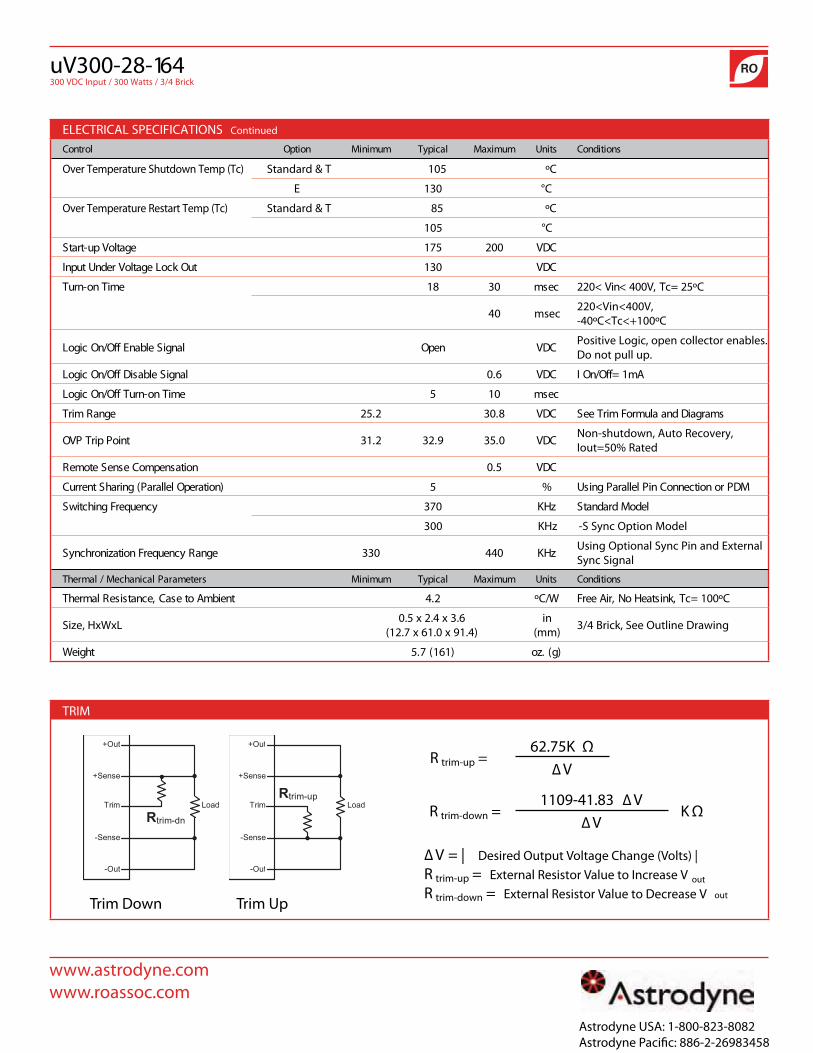
uV300-28-164 300 VDC Input / 300 Watts / 3/4 Brick
TRIM
Trim Down Trim Up
∆ V = | Desired Output Voltage Change (Volts) |R trim-up = External Resistor Value to Increase V out
R trim-down = External Resistor Value to Decrease V out
R trim-up =62.75K Ω
∆ V
R trim-down =1109-41.83 ∆ V
K Ω∆ V
ELECTRICAL SPECIFICATIONS Continued
snoitidnoCstinUmumixaMlacipyTmuminiMnoitpOlortnoC
Over Temperature Shutdown Temp (Tc) Standard & T 105 ºC
C°031E
Over Temperature Restart Temp (Tc) Standard & T 85 ºC
105 °C
CDV002571egatloV pu-tratS
CDV031tuO kcoL egatloV rednU tupnI
Cº52=cT ,V004<niV<022cesm0381emiT no-nruT
40 msec 220<Vin<400V,-40ºC<Tc<+100ºC
CDVnepOlangiS elbanE ffO/nO cigoL Positive Logic, open collector enables. Do not pull up.
Am1=ffO/nO ICDV6.0langiS elbasiD ffO/nO cigoL
cesm015emiT no-nruT ffO/nO cigoL
smargaiD dna alumroF mirT eeSCDV8.032.52egnaR mirT
CDV0.539.232.13tnioP pirT PVO Non-shutdown, Auto Recovery, Iout=50% Rated
CDV5.0noitasnepmoC esneS etomeR
MDP ro noitcennoC niP lellaraP gnisU%5)noitarepO lellaraP( gnirahS tnerruC
ledoM dradnatSzHK073ycneuqerF gnihctiwS
300 KHz -S Sync Option Model
zHK044033egnaR ycneuqerF noitazinorhcnyS Using Optional Sync Pin and External Sync Signal
snoitidnoCstinUmumixaMlacipyTmuminiMsretemaraP lacinahceM / lamrehT
Cº001=cT ,knistaeH oN ,riA eerFW/Cº2.4tneibmA ot esaC ,ecnatsiseR lamrehT
Size, HxWxL 0.5 x 2.4 x 3.6(12.7 x 61.0 x 91.4)
in(mm) 3/4 Brick, See Outline Drawing
)g( .zo)161( 7.5thgieW
www.astrodyne.comwww.roassoc.com
Astrodyne USA: 1-800-823-8082Astrodyne Pacic: 886-2-26983458

uV300-28-164 300 VDC Input / 300 Watts / 3/4 Brick
OUTPUT CHARACTERISTIC, Vin=300V, TC=25ºC
EFFICIENCY VS. LOAD, Vin=300V
TRANSIENT RESPONSE, Vin=300V, Iout=2.2A-8.8A-2.2A, Tc=25ºC
OUTPUT RIPPLE, Vin=300V, Iout=11.0A, Tc=25ºC
LOSSES VS. LOAD, Vin=300V
Loss
es (W
)E
cien
cy (%
)
Output Current (A)
Out
put V
olta
ge (V
)
Output Current (% of Full Load)
t, 1µs/div. 30MHz BWL
Output Current (A)
lout
, 2.2
A/d
iv.
V
out,
1.0V
/div
.
t, 100µs/div. 30MHz BWL Current Slew Rate 0.5A/ µs
65
70
75
80
85
90
0 2.0 4.0 6.0 8.0 10.0
TC = 25°CTC = 100°C
INPUT CHARACTERISTIC, Iout = 11.0A, TC=25ºC
0
5
10
15
20
25
30
35
40
45
50
0.0 2.0 4.0 6.0 8.0 10.0
TC = 25°CTC = 100°C
Inpu
t Cur
rent
(A)
0
5
10
15
20
25
30
0 20 40 60 80 100 120 140 160
Input Voltage (V)
0.0
0.5
1.0
1.5
2.0
0 50 100 150 200 250 300 350 400
50mVperdiv.
www.astrodyne.comwww.roassoc.com
Astrodyne USA: 1-800-823-8082Astrodyne Pacic: 886-2-26983458

uV300-28-164 300 VDC Input / 300 Watts / 3/4 Brick
OUTLINE DRAWING Dimensions in Inches
NOTES
REV 090410
www.astrodyne.comwww.roassoc.com
Astrodyne USA: 1-800-823-8082Astrodyne Pacic: 886-2-26983458

4 Ways to Order
Call (800) 823-8082 Toll Free or (508) 964-6300Service hours are 8:30am - 5:30 pm ESTMonday through Friday(excluding holidays)
Order Online at: www.astrodyne.com
Fax Order to: (508)339-0375
Email to: [email protected]
35 Hampden Road, Mansfield, MA 02048Tel: (508) 964-6300 Fax: (508) 339-0375