Embed Size (px)
Citation preview

"
DD CC && UU PP SS SS YY SS TT EE MM
Kingdom of Saudi Arabia Saline Water Conversion Corporation General Directorate of Training Programs Training Center – JUBAIL
Version 1.1 Prepared by: ABDUL-RAZIK OTHMAN BAKRY Date: FEBRUARY, 2007
MM AA II NN TT EE NN AA NN CC EE DD EE PP AA RR TT MM EE NN TT
EE LL EE CC TT RR II CC AA LL EE NN GG II NN EE EE RR SS CC OO MM MM OO NN
CC OO UU RR SS EE


Contents i
Contents Lesson 1: INTRODUCTION…………………………………………1
UNINTERRUPTIBLE POWER SUPPLIES (UPS)……………………………………….1 DC ESSENTIAL SUPPLIES……………………………1 AC ESSENTIAL SUPPLIES…………………….………2 CAPACITORS IN ELECTRONIC CIRCUITS………………………………………….……..2 CAPACITOR TYPES, SYMBOLS AND RATINGS…………………………………….……..4 NON-POLARISED CAPACITORS……………….…….4 POLARISED CAPACITOR………………….….……….4 SYMBOLS AND RATINGS……………………..………5 CAPACITOR CHARGE AND DISCHARGE……………………………………..………5 PRACTICAL EXERCISE - TESTING OF CAPACITORS………………………..…………….7 PRECAUTIONS…………………………..……….…….7 PROCEDURE……………………………………………8 RESULTS TABLE……………………………………….8 CONCLUSIONS ………………………………………...8 EXERCISE MARKING SCALE…………………………9
Lesson 2: COMMON COLLECTOR CONFIGURATION…………1
PN JUNCTION DIODE…………………………………..1 REVERSE BIAS…………………………………………..1 FORWARD BIAS……………………………….…………2 RATINGS, SYMBOLS AND PACKAGES………..……..2 PRACTICAL EXERCISE - TESTING DIODES…..…….3 PRECAUTIONS……………………………………..…….3 PROCEDURE………………………………..……………3 RESULTS TABLE………………………..……………….4 CONCLUSIONS…………………………..………………4 EXERCISE MARKING SCALE……………...…………..5 ZENERS AND LEDS………………………...…………...5 ZENER DIODE…………………………………………….5 LIGHT EMITTING DIODE (LED)…………..……………6 SYMBOLS AND PACKAGES……………..…………….7 BIPOLAR JUNCTION TRANSISTOR (BJT)…..……….7 BJT SYMBOLS AND PACKAGING……………….……8 TRANSISTOR CIRCUITS………………………….……9 COMMON EMITTER CONFIGURATION……….…….10 SEMICONDUCTOR DEVICES………………….……..11
Lesson 3: UNCONTROLLED RECTIFIERS……………………….1 DC ESSENTIAL SUPPLIES………………………….....1 HALF WAVE RECTIFIER…………………..……………2 FULL WAVE RECTIFIERS…………………...………….3

Contents ii
CENTRE-TAP TRANSFORMER RECTIFIER......……3 BRIDGE RECTIFIER……………………………...……..4 THREE PHASE BRIDGE RECTIFIER…………………5 RECTIFIER CIRCUIT……………………………………5 PRV AND RIPPLE……………………………………….7 PRACTICAL EXERCISE - RECTIFIER WAVEFORMS…………………………………………..7 OBJECTIVES……………………………………………7 GENERAL PRECAUTIONS……………………………7 SPECIAL PRECAUTIONS WHEN USING ANOSCILLOSCOPE……………………………..…….8 EQUIPMENT……………………………………………8 PROCEDURE…………………………………………..8 Half Wave Rectifier…………………………………….8 Bridge Rectifier…………………………………………8 RESULTS TABLE……………………………………..9 CONCLUSIONS……………………………………….9 EXERCISE MARKING SCALE……………………..10
Lesson 4: DC FILTERS……………………………………………1 SHUNT CAPACITOR FILTER…………………….….1 FILTER ACTION…………………………………….…1 WAVEFORM AND RIPPLE…………………………..2 PRV RATINGS………………………………………...3 FILTERED HALF-WAVE RECTIFIER…………….…4 FILTERED FULL-WAVE RECTIFIERS……….……..4 PRACTICAL DEMONSTRATION……………….……4 OTHER TYPES OF FILTER……………………….….4 SERIES INDUCTOR FILTER…………………………4 PI FILTER ………………………………………………5
Lesson 5: VOLTAGE REGULATORS…………………………..1 ZENERSERIES EGULATOR………………………...1 ZENER FOLLOWER……………….…………………1 NEGATIVE FEEDBACK…………..…………………2 CURRENT LIMITING………………...……………….2 ZENER SHUNT REGULATOR…………………..…..4 SWITCHING REGULATOR…………………………..5 BASIC OPERATION……………………….………….5 PULSE GENERATOR…………………….…………..6 OPERATIONAL AMPLIFIER…………………………7 BASIC 741C OP-AMP……………………..………….7 NEGATIVE FEEDBACK……………………..……….9 LM340 VOLTAGE REGULATOR………..………….12
Lesson 6: SILICON CONTROLLED RECTIFIERS…………….1 SCR BASIC THEORY…………………………………1 INTRODUCTION……………………………………….1 CONSTRUCTION AND CIRCUIT SYMBOL………...1 SCR OPERATION………………………………….…..2

Contents iii
COMPARISON WITH DIODE……………………………3 RATINGS AND PACKAGES……………………….…….3 PRACTICAL EXERCISE - TESTING AN SCR WITH A MULTIMETER………………………..4 PRECAUTIONS……………………………………………4 PROCEDUR………………………………………………..4 RESULTS TABLE………………………………….………4 CONCLUSIONS……………………………………………4 EXERCISE MARKING SCALE………………….………..5 PRACTICAL EXERCISE - DC TESTS OF AN SCR……………………………………….5 OBJECTIVES………………………………………………5 PRECAUTIONS……………………………………………5 EQUIPMENT……………………………………………….5 PROCEDUR ……………………………………………….5 RESULTS TABLE………………………………………….6 CONCLUSIONS……………………………………………7 EXERCISE MARKING SCALE………………….………..7
Lesson 7: INVERTERS………………………………………………..1
AC ESSENTIAL SUPPLIES………………………………1 INVERSION………………………………………………...2 INVERTER SYMBOL……………………………………...2 CENTRE-TAP TRANSFORMER INVERTER (HALF BRIDGE)……………………………..2 FULL BRIDGE INVERTER…………………………….…4 INVERTING OPERATION………………………………..4 BLOCKING THE INVERTING SCRS……………………5 FREEWHEELING AN INDUCTIVE LOAD………………6 VOLTAGE REGULATION………………………………..6 THREE-PHASE INVERTERS…………………………...7 THREE-PHASE FOUR-WIRE INVERTER……………..7 THREE-PHASE BRIDGE INVERTER…………………..8
Lesson 7: INVERTER AUXILIARIES……………………………….1 HARMONIC FILTERS……………………………………1 SERIES RESONANT FILTER…………………………..1 SHUNT RESONANT FILTER…………………………...3 TRANSFORMERS AND STATIC SWITCH……………5 TRANSFORMERS……………………………………….5 STATIC SWITCH…………………………………..…….6 SCR TRIGGERING………………………………………8

Uninterrupted Power Supply Introduction
Lesson 1 Page 1
LESSON 1
LECTURE INTRODUCTION
Objectives
At the end of this Lesson, the Trainee will be able to explain what DC and AC UPS systems are and how they work; state that capacitors are dangerous and correctly discharge them; identify polarized capacitors; calculate RC Time Constants; test capacitors using MultiMate’s.
1 UNINTERRUPTIBLE POWER SUPPLIES (UPS)
1.1 DC ESSENTIAL SUPPLIES
There are many important controls which must have a reliable supply of electricity. Some typical examples are the tripping & closing coils of circuit breakers and the protection relays which operate these in emergencies. These are essential loads. Such equipment where any loss of power is not acceptable is supplied with DC current. Normally a Rectifier supplies the essential DC loads and also charges up a Battery. This is called a DC Essential Supply. If the DC supply from the rectifier fails, the battery supplies the load without any interruption of current. The battery can only provide DC power for a few hours, determined by its Ampere-Hour Capacity and the current drawn by the DC load. Meanwhile arrangements can be made to restore DC power from the charger.
Fig. 1-1. Dual Redundant DC Power Supply
~
~
--
--
AC MAINS
AC MAINS
RECTIFIER/CHARGE
RECTIFIER/CHARGE
BATTERY
BATTERY
-
+
-
DC BUSBAR
DC
LOAD
LOAD
+
+
-
-
BUS
Uninterrupted Power Supply Introduction
Lesson 1 Page 2
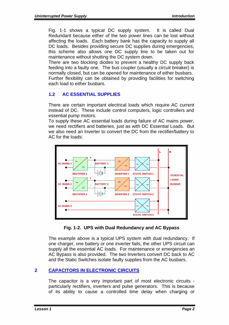
Fig. 1-1 shows a typical DC supply system. It is called Dual Redundant because either of the two power lines can be lost without affecting the loads. Each battery bank has the capacity to supply all DC loads. Besides providing secure DC supplies during emergencies, this scheme also allows one DC supply line to be taken out for maintenance without shutting the DC system down. There are two blocking diodes to prevent a healthy DC supply back feeding into a faulty one. The bus coupler (usually a circuit breaker) is normally closed, but can be opened for maintenance of either busbars. Further flexibility can be obtained by providing facilities for switching each load to either busbars. 1.2 AC ESSENTIAL SUPPLIES There are certain important electrical loads which require AC current instead of DC. These include control computers, logic controllers and essential pump motors. To supply these AC essential loads during failure of AC mains power, we need rectifiers and batteries, just as with DC Essential Loads. But we also need an Inverter to convert the DC from the rectifier/battery to AC for the loads:
~
~
---
---
AC MAINS 1
AC MAINS 2
RECTIFIER 1
RECTIFIER 2
BATTERY 1
BATTERY 2
ESSENTIAL
+
+
-
----
~
---
~ INVERTER 1
INVERTER 2
L N
~ ~
LOADS
STATIC SWITCH 1
~ ~
STATIC SWITCH 2
BUSBAR
~ ~
STATIC SWITCH 3
AC MAINS 3
Fig. 1-2. UPS with Dual Redundancy and AC Bypass
The example above is a typical UPS system with dual redundancy. If one charger, one battery or one inverter fails, the other UPS circuit can supply all the essential AC loads. For maintenance or emergencies an AC Bypass is also provided. The two Inverters convert DC back to AC and the Static Switches isolate faulty supplies from the AC busbars.
2 CAPACITORS IN ELECTRONIC CIRCUITS The capacitor is a very important part of most electronic circuits - particularly rectifiers, inverters and pulse generators. This is because of its ability to cause a controlled time delay when charging or

Uninterrupted Power Supply Introduction
Lesson 1 Page 3
discharging through a series resistance. So the capacitor can switch circuits on and off. Capacitors are dangerous because they store electrical charge and can electrocute anyone who touches their terminals. It is therefore very important to discharge a capacitor before working on it. This is done by shorting the two terminals together with a jumper lead. Large capacitors should be discharged through a resistor, to limit the discharge current. This avoids large arcs being produced. Because capacitors are so important in electronics, it is useful to remember their most important features: 1. A capacitor is simply two metal plates separated by a Dielectric (insulating material). When a DC voltage is applied to the plates current cannot flow through the dielectric, but there is a charge build-up on the plates. 2. The ability of a capacitor to store charge is its Capacitance. This is measured in Farads. The relationship between charge (Q), capacitance (C) and voltage (V) is: Q = C x V. 3. Since it stores charge a capacitor opposes voltage changes. When the supply voltage to a DC circuit falls to zero volts, the capacitor will maintain voltage in the circuit. This is why even small capacitors are very dangerous and must be discharged before they are touched. However, this ability of the capacitor to maintain voltage is very useful in many electronic circuits. 4. When the supply voltage is AC the capacitor charges in one direction, then discharges and charges in the opposite direction as the supply voltage alternates. So current flows all the time. The Reactance of the capacitor is high for low frequencies and low for high frequencies: XC = 1_ = -j__ jωC 2πfC The -j signifies that XC is the opposite of Inductive Reactance. This ability of capacitance to cancel out inductance is used in Series and Parallel Resonant circuits (oscillators and filters). 5. When capacitors are connected in parallel the total capacitance, CT, is:
CT = C1 + C2 + C3 + ............ But when capacitors are connected in series, CT is given by: 1_ = 1_ + 1_ + 1_ + ............ CT C1 C2 C3 6. Capacitor Identification Typical capacitor packages are shown in Fig. 1-3:

Uninterrupted Power Supply Introduction
Lesson 1 Page 4
Fig. 1-3 - CAPACITOR PACKAGES Most capacitors have leads for solder connections, though high-capacity units have bolt-and-thread connections. 7. The Farad (F) is a very large unit. Most electronic circuits use very small capacitors of typical sizes: - Micro-Farads (µF), equal to 10-6 F - Nano-Farads (nF), equal to 10-9 F - Pico-Farads (pF), equal to 10-12 F
3 CAPACITOR TYPES, SYMBOLS AND RATINGS There are two different designs of capacitor in common use, Polarized (Electrolytic) and Non-Polarized (Electrostatic). It is very important to understand the differences between them. 3.1 NON-POLARISED CAPACITORS This is of standard, two-plate, construction. The dielectric can be ceramic, mica, paper or plastic compounds. It does not matter which plate is positive, so it is suitable for AC circuits. 3.2 POLARISED CAPACITOR This capacitor contains an electrolyte (like a battery) rather than a dielectric. The plates are usually of aluminum or tantalum. Because it contains an electrolyte, the capacitor is polarized - it acts as a good insulator (capacitor) in one direction, but as a good conductor (short circuit) in the other. If the supply voltage positive is applied to the capacitor positive terminal we have a good capacitor. But if the supply voltage positive is applied to the capacitor negative terminal, and the voltage is large enough, the dielectric breaks down to a short circuit and the capacitor explodes. (A very small reverse voltage, such as that from an ohmmeter, will not cause any damage.) Despite this danger, polarized capacitors can store much more charge than similar sized non-polarized capacitors (though they lose charge through leakage much more quickly). They are therefore widely used in DC circuits, especially rectifier filters. A polarized capacitor can be recognized by its polarity marking (non-polarized capacitors do not have any polarity markings). Some typical markings are shown in Fig. 1-4:

Uninterrupted Power Supply Introduction
Lesson 1 Page 5
_
IDENTIFY CATHODE (NEGATIVE TERMINAL)
_ + +IDENTIFY ANODE
(POSITIVE TERMINAL)
Fig. 1-4. Polarity Markings
3.3 SYMBOLS AND RATINGS Typical circuit symbols are shown in Fig. 1-5:
OR ELECTROSTATIC (NON-POLARISED)
OR+
ELECTROLYTIC (POLARISED) +
OR VARIABLE NON-POLARISED
Fig. 1-5. Circuit Symbols The two important ratings for a capacitor are: 1. Nominal Capacitance, given in pF, nF or µF. 2. Nominal Voltage, which is DC unless stated otherwise. The AC rms voltage rating of a non-polarized capacitor is approximately 70% of the DC rating (to limit the peak value of the waveform). For most capacitors, these two ratings are engraved on the case. On some small capacitors a colour coding system is used, rather like that for carbon resistors. Many small capacitors only have a reference code. To find the ratings, these capacitors must be tested or the manufacturer’s reference book consulted.
4 CAPACITOR CHARGE AND DISCHARGE When a DC voltage is applied to a capacitor, there is a surge of current as the capacitor charges up. This current rapidly reduces to zero as voltage builds up across the capacitor plates. This process is called charging. The supply voltage can now be switched off and the capacitor retains its voltage!

Uninterrupted Power Supply Introduction
Lesson 1 Page 6
If the capacitor terminals are now shorted out, the capacitor discharges and once again a surge of current flows, which rapidly reduces to zero as the voltage across the plates is lost. The larger the capacitor (or resistor) the larger the charge/discharge currents and the longer the time taken to charge and discharge. We can prolong the charge and discharge times and reduce the surge currents by adding series resistance to the circuit, as shown in Fig. 1-6:
R
C
(a) CAPACITOR CHARGING
C
R
(b) CAPACITOR DISCHARGING
Fig. 1-6. RC Time-delay circuit
A measure of the time delay for charge and discharge is the RC Time Constant (T).This is the time taken for the voltage to change by 63.2 %. Mathematically:
T = R x C Example A 10 µF capacitor is in series with a 100 kΩ resistor. A DC supply of 20 V is applied. Calculate: (a) The RC Time Constant (T). (b) The voltage across C when this time has elapsed. Answer: (a) T = RC = 100 x 103 x 10 x 10-6 = 1 second (b) V = 0.632 x E = 0.632 x 20 = 12.64 V Fig. 1-7 on the next page shows typical Voltage/Time and Current Time graphs for charging a capacitor - first with a small series resistor and next with a large resistor. These graphs will invert for capacitor discharge, because the voltage will reduce and the current will be negative (reverse flow).

Uninterrupted Power Supply Introduction
Lesson 1 Page 7
Emax
63.2% Small R (small RC Time Constant)
Large R (large RC Time Constant)
timeT2T1
Imax
26.8%
T1 T2
Small R (small RC Time Constant)
Large R (large RC Time Constant)
time
Fig. 1-7. Effect of varying the Series Resistor
The RC Time Constant is used when testing a capacitor with an analogue MultiMate on its ohm function. The circuit is the same as Fig. 1-6, because the series resistance is built into the meter. So we can flick-test the capacitor. The meter pointer should flick towards zero ohms (maximum current) then slowly move back towards infinite ohms (zero current). If this does not happen, either the meter range is too low to measure the capacitor, or the capacitor is damaged. The following exercise is designed to give the trainee practice in testing capacitors and extracting information on ratings and construction.
5 PRACTICAL EXERCISE - TESTING OF CAPACITORS 5.1 PRECAUTIONS 1. Always discharge a capacitor before touching it. A large, charged capacitor CAN ELECTROCUTE YOU! 2. When testing, do not press the bare ends of the test probes onto the component with your fingers. The resistance of your body will be in parallel with the component. This will give inaccurate readings. 3. When using any MultiMate as an ohm-meter, always check that the batteries are fully charged. A low-charged battery will not give accurate readings, because it cannot supply enough power for the test circuit.

Uninterrupted Power Supply Introduction
Lesson 1 Page 8
4. When using an analogue meter as an ohm-meter, always set the zero reading, by shorting the meter leads together, before testing. Do this for each range multiplier you use before testing the component. 5.2 PROCEDURE There are 3 capacitors, labeled 1 to 3. For each one: 1. Determine the nominal capacitance, nominal voltage and whether the capacitor is polarized or not, by reading the information on the case. 2. Measure the capacitance using the digital MultiMate as a Capacitance Meter. Record the values in the Results Table, with the range setting used. 3. Use the analogue meter as an ohm-meter to perform a Flick Test. Record whether the test was successful or not and which Scale Multiplier was used. 4. Repeat step 3 using the digital MultiMate. Record whether the test was successful or not and which range setting was used.
5.3 RESULTS TABLE
CAPA-
CITOR
PACKAGE INFORMATION
DIGITAL METER
AS CAPACITAN
CE METER
ANALOGUE METER
FLICK TEST
DIGITAL METER FLICK TEST
CAP
A-CITOR
NO. NOMINAL
CAPAC-
ITANCE
NOMINAL
VOLTAGE
POLA-
RISED
(Y/N)
READING
SCALE
RANGE
TEST
OK? (Y/N)
MULTI-PLIER
TEST OK? (Y/N)
SCALE
RANGE
OK?(Y/N)
1 0.1 µF 100
VDC NO 0.1 µF 2 µF Y R x 10K Y 2 MΩ Y
2 0.22 µF 50 VDC NO 0.2 µF 2 µF Y R x 10K Y 2 MΩ Y
3 10 µF 35 VDC YES 10 µF 20 µF Y R x 10K Y 2 MΩ Y
5.4 CONCLUSIONS 1. Which of the three tests is the easiest to perform accurately and gives the most information? Why? Answer: DIGITAL METER AS CAPACITANCE METER, WHICH NOT ONLY SHOWS CAPACITOR IS OK, BUT MEASURES CAPACITANCE TOO. 2. Which MultiMate is best for performing Flick Tests? Why?

Uninterrupted Power Supply Introduction
Lesson 1 Page 9
Answer:ANALOGUE METER AS OHMMETER, AS IT IS EASY TO SEE THE CHARGE & DISCHARGE OF THE CAPACITOR. 5.5 EXERCISE MARKING SCALE 1. Observations Nominal Capacitance - 3 x 2 points = 6 points Nominal Voltage - 3 x 2 points = 6 points Polarized (Y/N) - 3 x 4 points = 12 points Sub-Total = 24 points 2. Practical Tests Capacitance Reading - 3 x 4 points = 12 points Capacitance Meter Range - 3 x 2 points = 6 points Analogue Meter Flick Test - 3 x 3 points = 9 points Analogue Scale Multiplier - 3 x 3 points = 9 points Digital Meter Flick Test - 3 x 3 points = 9 points Digital Scale Range - 3 x 3 points = 9 points Sub-Total = 54 points 3. Conclusions Capacitor OK? - 3 x 2 points = 6 points Conclusion 1 - = 8 points Conclusion 2 - = 8 points Sub-Total = 22 points OVERALL TOTAL = 100 Points

Uninterrupted Power Supply Semiconductor Devices
Lesson 2 Page 1
LESSON 2
LECTURE SEMICONDUCTOR DEVICES
Objectives
At the end of this Lesson, the Trainee will be able to explain the construction and operation, identify circuit symbols and packages, and test the most common semiconductor devices used in electronic circuits.
1 PN JUNCTION DIODE
The PN Junction Diode only conducts electricity one way, from Anode to Cathode. If current tries to flow the wrong way (from Cathode to Anode) the diode blocks it. So the diode acts just like a check valve in a water system. The diode is called a PN Junction Diode because it is made of one piece of P-Type material (containing positive Holes) and one piece of N-Type material (containing negative Free Electrons) with a Junction between them. Around the Junction is a Barrier (Depletion) Region where there are no holes or electrons. 1.1 REVERSE BIAS
P - TYPE N - TYPE
BARRIER VOLTAGEVB
HOLESELECTRONSBARRIER REGION
(DEPLETION REGION)
E
(+)(-)
E = VB
Fig. 2-1. Reverse Bias (no conduction)
As shown in Fig. 2-1, with the battery positive connected to the N - Type material the Depletion Region grows bigger so that the Barrier Voltage, VB, always equals the applied EMF, E. So no current flows. This is called Reverse Bias.
Uninterrupted Power Supply Semiconductor Devices
Lesson 2 Page 2
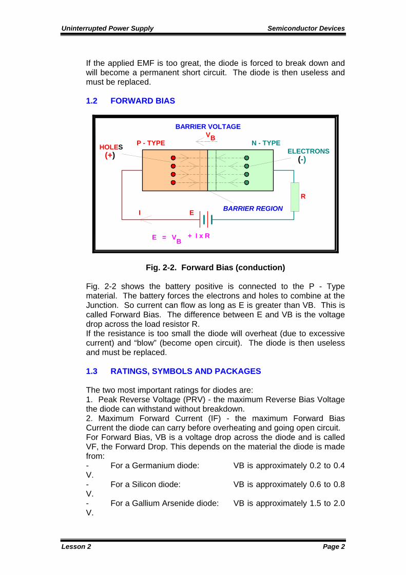
If the applied EMF is too great, the diode is forced to break down and will become a permanent short circuit. The diode is then useless and must be replaced. 1.2 FORWARD BIAS
P - TYPE N - TYPE
BARRIER VOLTAGEVB
BARRIER REGIONE
(+) (-)HOLES ELECTRONS
I
R
E = VB + I x R
Fig. 2-2. Forward Bias (conduction) Fig. 2-2 shows the battery positive is connected to the P - Type material. The battery forces the electrons and holes to combine at the Junction. So current can flow as long as E is greater than VB. This is called Forward Bias. The difference between E and VB is the voltage drop across the load resistor R. If the resistance is too small the diode will overheat (due to excessive current) and “blow” (become open circuit). The diode is then useless and must be replaced. 1.3 RATINGS, SYMBOLS AND PACKAGES The two most important ratings for diodes are: 1. Peak Reverse Voltage (PRV) - the maximum Reverse Bias Voltage the diode can withstand without breakdown. 2. Maximum Forward Current (IF) - the maximum Forward Bias Current the diode can carry before overheating and going open circuit. For Forward Bias, VB is a voltage drop across the diode and is called VF, the Forward Drop. This depends on the material the diode is made from: - For a Germanium diode: VB is approximately 0.2 to 0.4 V. - For a Silicon diode: VB is approximately 0.6 to 0.8 V. - For a Gallium Arsenide diode: VB is approximately 1.5 to 2.0 V.
Uninterrupted Power Supply Semiconductor Devices
Lesson 2 Page 3
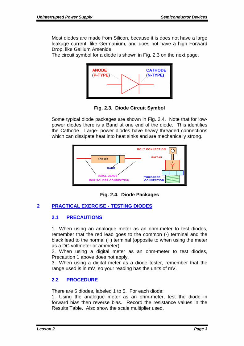
Most diodes are made from Silicon, because it is does not have a large leakage current, like Germanium, and does not have a high Forward Drop, like Gallium Arsenide. The circuit symbol for a diode is shown in Fig. 2.3 on the next page.
ANODE (P-TYPE)
CATHODE (N-TYPE)
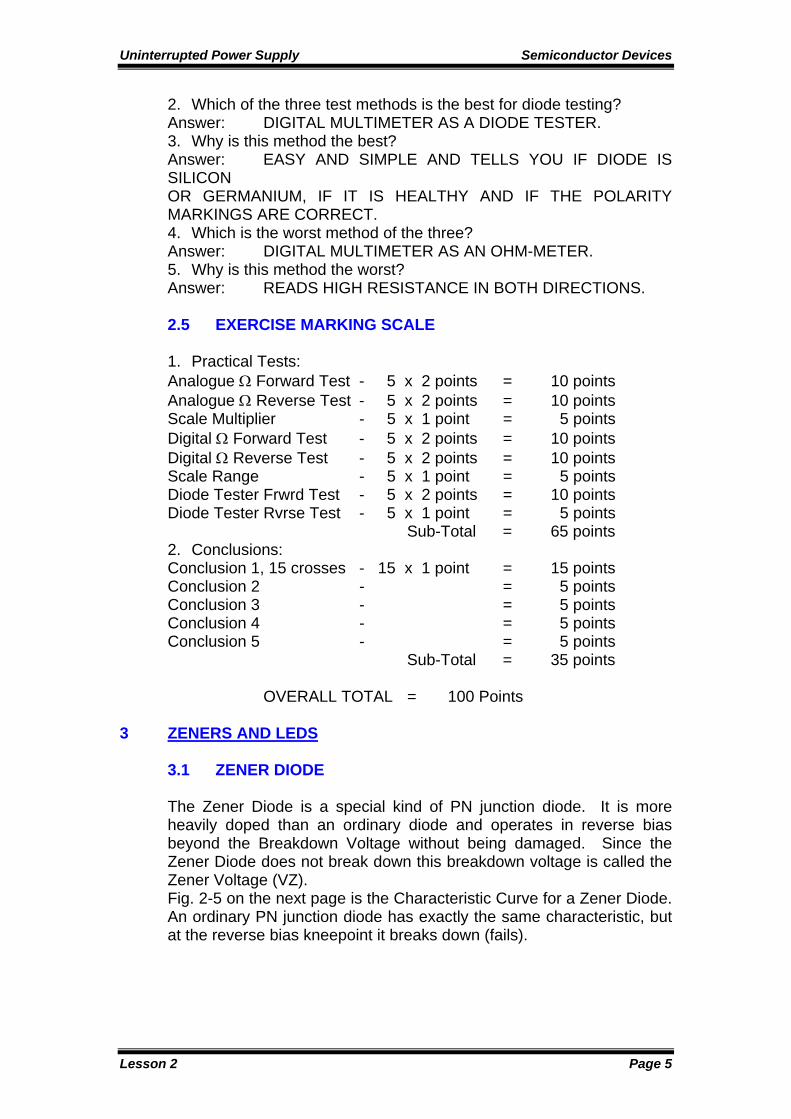
Fig. 2.3. Diode Circuit Symbol Some typical diode packages are shown in Fig. 2.4. Note that for low-power diodes there is a Band at one end of the diode. This identifies the Cathode. Large- power diodes have heavy threaded connections which can dissipate heat into heat sinks and are mechanically strong.
1N4004
BAND
AXIAL LEADS
FO R SOLDER CO NNECTIO N
PIGTAIL
THREADED CO NNECTIO N
BO LT CO NNECTION
Fig. 2.4. Diode Packages
2 PRACTICAL EXERCISE - TESTING DIODES 2.1 PRECAUTIONS 1. When using an analogue meter as an ohm-meter to test diodes, remember that the red lead goes to the common (-) terminal and the black lead to the normal (+) terminal (opposite to when using the meter as a DC voltmeter or ammeter). 2. When using a digital meter as an ohm-meter to test diodes, Precaution 1 above does not apply. 3. When using a digital meter as a diode tester, remember that the range used is in mV, so your reading has the units of mV. 2.2 PROCEDURE There are 5 diodes, labeled 1 to 5. For each diode: 1. Using the analogue meter as an ohm-meter, test the diode in forward bias then reverse bias. Record the resistance values in the Results Table. Also show the scale multiplier used.

Uninterrupted Power Supply Semiconductor Devices
Lesson 2 Page 4
2. Using the digital meter as an ohm-meter, test the diode in forward bias then reverse bias. Record the resistance values in the Results Table. Also show the range used. 3. Test the diode with the digital meter as a diode tester. Record the voltages measured in the Results Table. 2.3 RESULTS TABLE
DIODE
ANALOGUE OHMMETER
DIGITAL
OHMMETER
DIGITAL
DIODE TESTER
NO. + -Ω
+ -Ω
SCALEMULTI-PLIER
+ -Ω
+ -Ω
SCALERANGE
+ -mV
+ -mV
1 12 Ω ∞ x 1 ∞ ∞ 20 MΩ 600 mV ∞
2 10 Ω ∞ x 1 ∞ ∞ 20 MΩ 630 mV ∞
3 15 Ω ∞ x 1 ∞ ∞ 20 MΩ 700 mV ∞
4 ∞ ∞ x 10 K ∞ ∞ 20 MΩ ∞ ∞
5 0.1 Ω 0.1 Ω x 1 0.1 Ω 0.1 Ω 200 Ω 0 0
2.4 2.4 CONCLUSIONS 1. From your test results, complete the Table below by placing a tick (√) in the correct boxes:
DIODE
DIODE CONDITION
CATHODE
IDENTIFICATION
DIODE MATERIAL
NO. HEALTHY
OPENCIRCUI
T
SHORTCIRCUI
T
CORRECT
WRONG
? SILICON GERM-ANIUM
?
1 √ √ √
2 √ √ √
3 √ √ √
4 √ √ √
5 √ √ √
Uninterrupted Power Supply Semiconductor Devices
Lesson 2 Page 5
2. Which of the three test methods is the best for diode testing? Answer: DIGITAL MULTIMETER AS A DIODE TESTER. 3. Why is this method the best? Answer: EASY AND SIMPLE AND TELLS YOU IF DIODE IS SILICON OR GERMANIUM, IF IT IS HEALTHY AND IF THE POLARITY MARKINGS ARE CORRECT. 4. Which is the worst method of the three? Answer: DIGITAL MULTIMETER AS AN OHM-METER. 5. Why is this method the worst? Answer: READS HIGH RESISTANCE IN BOTH DIRECTIONS. 2.5 EXERCISE MARKING SCALE 1. Practical Tests: Analogue Ω Forward Test - 5 x 2 points = 10 points Analogue Ω Reverse Test - 5 x 2 points = 10 points Scale Multiplier - 5 x 1 point = 5 points Digital Ω Forward Test - 5 x 2 points = 10 points Digital Ω Reverse Test - 5 x 2 points = 10 points Scale Range - 5 x 1 point = 5 points Diode Tester Frwrd Test - 5 x 2 points = 10 points Diode Tester Rvrse Test - 5 x 1 point = 5 points Sub-Total = 65 points 2. Conclusions: Conclusion 1, 15 crosses - 15 x 1 point = 15 points Conclusion 2 - = 5 points Conclusion 3 - = 5 points Conclusion 4 - = 5 points Conclusion 5 - = 5 points Sub-Total = 35 points OVERALL TOTAL = 100 Points
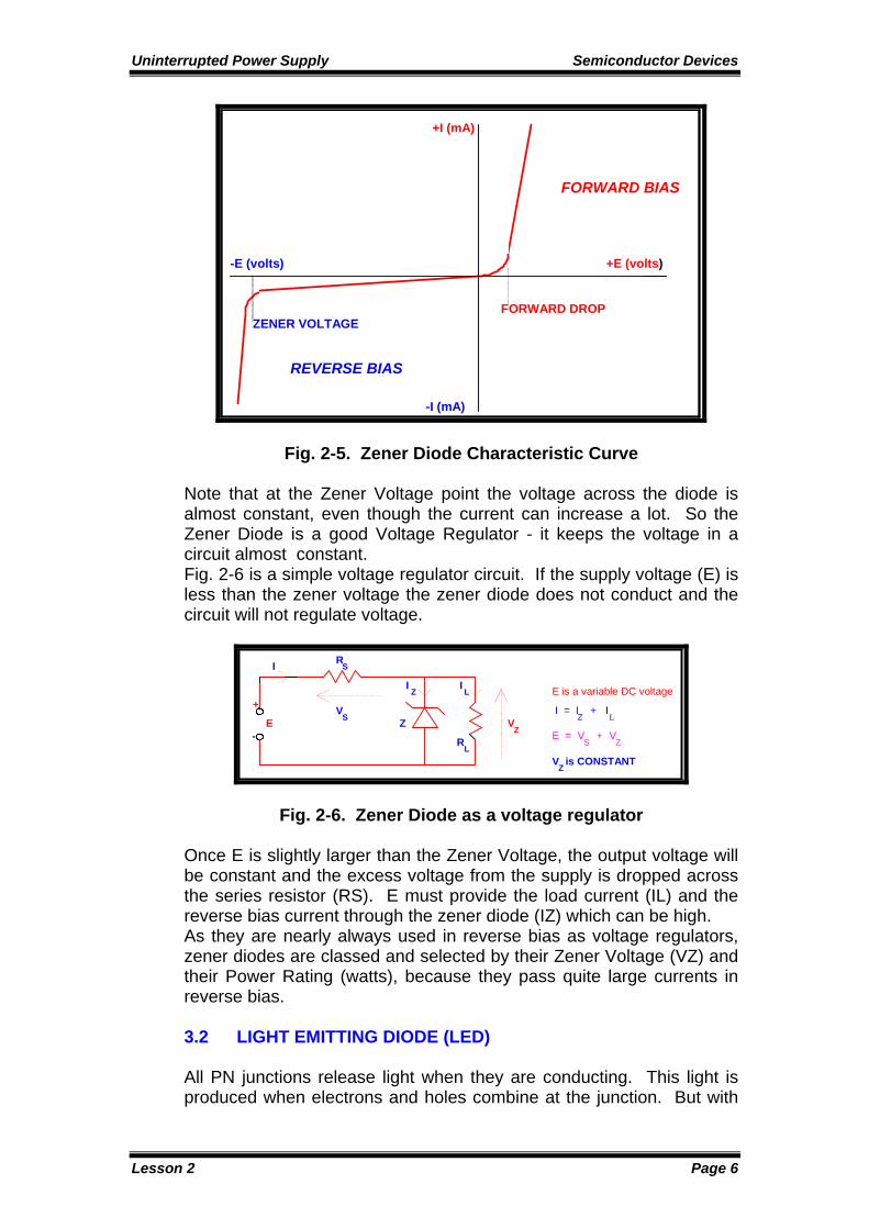
3 ZENERS AND LEDS 3.1 ZENER DIODE The Zener Diode is a special kind of PN junction diode. It is more heavily doped than an ordinary diode and operates in reverse bias beyond the Breakdown Voltage without being damaged. Since the Zener Diode does not break down this breakdown voltage is called the Zener Voltage (VZ). Fig. 2-5 on the next page is the Characteristic Curve for a Zener Diode. An ordinary PN junction diode has exactly the same characteristic, but at the reverse bias kneepoint it breaks down (fails).
Uninterrupted Power Supply Semiconductor Devices
Lesson 2 Page 6
+E (volts) -E (volts)
+I (mA)
-I (mA)
FORWARD DROP ZENER VOLTAGE
FORWARD BIAS
REVERSE BIAS
Fig. 2-5. Zener Diode Characteristic Curve Note that at the Zener Voltage point the voltage across the diode is almost constant, even though the current can increase a lot. So the Zener Diode is a good Voltage Regulator - it keeps the voltage in a circuit almost constant. Fig. 2-6 is a simple voltage regulator circuit. If the supply voltage (E) is less than the zener voltage the zener diode does not conduct and the circuit will not regulate voltage.
+
-
R
R
Z E
I I
V Z
Z L
L
I S
V S
E is a variable DC voltage
I = IZ
+ IL
E = V S
+ V Z
V Z
is CONSTANT
Fig. 2-6. Zener Diode as a voltage regulator Once E is slightly larger than the Zener Voltage, the output voltage will be constant and the excess voltage from the supply is dropped across the series resistor (RS). E must provide the load current (IL) and the reverse bias current through the zener diode (IZ) which can be high. As they are nearly always used in reverse bias as voltage regulators, zener diodes are classed and selected by their Zener Voltage (VZ) and their Power Rating (watts), because they pass quite large currents in reverse bias. 3.2 LIGHT EMITTING DIODE (LED) All PN junctions release light when they are conducting. This light is produced when electrons and holes combine at the junction. But with

Uninterrupted Power Supply Semiconductor Devices
Lesson 2 Page 7
silicon and germanium diodes the junction and package material are opaque, so no light is visible. The LED is a special diode. It produces visible light when it conducts. It is usually made of Gallium Arsenide and its forward drop is roughly 1.5 to 2.0 volts. The junction is encased in translucent plastic so that the emitted light can be seen. The plastic case is coloured, so that the light seen has the colour of the case. LEDs are used as indicators (warning lights and on/off lights) in electronic circuits. 3.3 SYMBOLS AND PACKAGES
ZENER DIODE
(a) CIRCUIT SYMBOLS
OR
LED
(b) PACKAGES
AXIAL LEAD BAND (CATHODE) TRANSLUCENT
CASING
OR
CATHODE
ANODE
Fig. 2-7. Symbols and packages Fig 2-7 shows ttypical circuit symbols and packages for Zener Diodes and LEDs.
4 BIPOLAR JUNCTION TRANSISTOR (BJT) The transistor is similar to a PN Junction Diode, but has two junctions instead of one. It can be either NPN type, or PNP type. The 3 terminals are the Collector, Base (much narrower and less heavily doped) and Emitter. Refer to Fig. 2-8 on the next page. Whether the transistor is NPN or PNP, there must be FORWARD BIAS on the BASE-EMITTER Junction before current can flow between the Collector and Emitter. The BJT transistor is therefore an excellent solid-state DC Switch.
For either type of transistor: IE = IB + IC

Uninterrupted Power Supply Semiconductor Devices
Lesson 2 Page 8
Typically, IC is 50 to 100 times larger than IB. So a small Base current can control a large Collector current. So the BJT transistor is an Amplifier.
N P N
R C
R B
E I c
IB
IE
NPN TRANSISTOR
N P N
R C
E
EMITTER BASE COLLECTOR
NP P
R C
E
EMITTER BASE COLLECTOR
PNP TRANSISTOR
NO BIAS on B-E
Junction, so NO
CURRENT in C-E
circuit.
R C
R B
E I c
IB
I E
WITH FORWARD
BIAS on the B-E
Junction, current
can NOW FLOW
in the C-E circuit.
N P P
Fig. 2-8. BJT Transistor Construction and Operation
5 BJT SYMBOLS AND PACKAGING The circuit symbols for NPN and PNP transistors are shown in Fig. 2-9. The arrow in the Emitter tells you which way the Base-Emitter P-N Junction is polarized, just like the triangle in the circuit symbol of a diode.
B
C
E
NPN TRANSISTOR
B
C
E
PNP TRANSISTOR
Fig. 2-9, Transistor Circuit Symbols
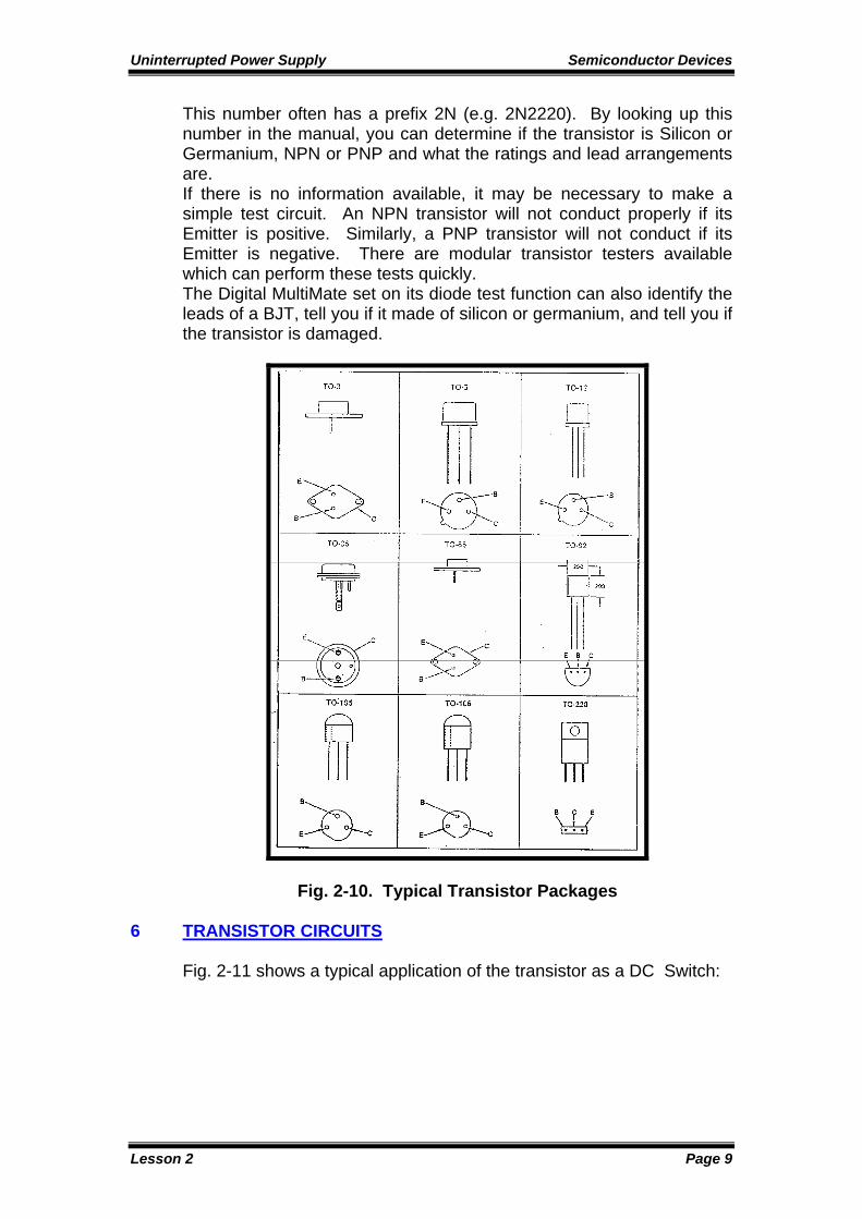
There are dozens of different packages and pin formations for transistors. Some of the most common are shown in Fig. 2-10 on the next page. Some packages (e.g. TO-5) are aluminum cans. Others (e.g. TO-92) are plastic encapsulated. TO-3 is a large power transistor with only two leads - the Base and Emitter. The metal casing is the Collector, which bolts to a heat sink. The Base can always be easily identified by testing with a MultiMate. If any doubt exists regarding which leads are the Collector and Emitter the manufacturer’s manual or other reference book should be consulted. First you must read the code number printed on the case.
Uninterrupted Power Supply Semiconductor Devices
Lesson 2 Page 9
This number often has a prefix 2N (e.g. 2N2220). By looking up this number in the manual, you can determine if the transistor is Silicon or Germanium, NPN or PNP and what the ratings and lead arrangements are. If there is no information available, it may be necessary to make a simple test circuit. An NPN transistor will not conduct properly if its Emitter is positive. Similarly, a PNP transistor will not conduct if its Emitter is negative. There are modular transistor testers available which can perform these tests quickly. The Digital MultiMate set on its diode test function can also identify the leads of a BJT, tell you if it made of silicon or germanium, and tell you if the transistor is damaged.
Fig. 2-10. Typical Transistor Packages
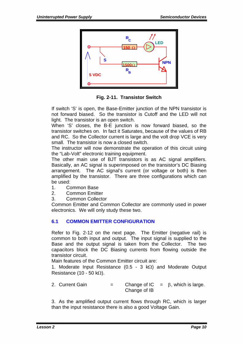
6 TRANSISTOR CIRCUITS Fig. 2-11 shows a typical application of the transistor as a DC Switch:
Uninterrupted Power Supply Semiconductor Devices
Lesson 2 Page 10
5 VDC
S
RC
150
1500R
B
LED
NPNΩ
Ω
Fig. 2-11. Transistor Switch If switch ‘S’ is open, the Base-Emitter junction of the NPN transistor is not forward biased. So the transistor is Cutoff and the LED will not light. The transistor is an open switch. When ‘S’ closes, the B-E junction is now forward biased, so the transistor switches on. In fact it Saturates, because of the values of RB and RC. So the Collector current is large and the volt drop VCE is very small. The transistor is now a closed switch. The instructor will now demonstrate the operation of this circuit using the “Lab-Volt” electronic training equipment. The other main use of BJT transistors is as AC signal amplifiers. Basically, an AC signal is superimposed on the transistor’s DC Biasing arrangement. The AC signal’s current (or voltage or both) is then amplified by the transistor. There are three configurations which can be used: 1. Common Base 2. Common Emitter 3. Common Collector Common Emitter and Common Collector are commonly used in power electronics. We will only study these two. 6.1 COMMON EMITTER CONFIGURATION Refer to Fig. 2-12 on the next page. The Emitter (negative rail) is common to both input and output. The input signal is supplied to the Base and the output signal is taken from the Collector. The two capacitors block the DC Biasing currents from flowing outside the transistor circuit. Main features of the Common Emitter circuit are: 1. Moderate Input Resistance (0.5 - 3 kΩ) and Moderate Output Resistance (10 - 50 kΩ). 2. Current Gain = Change of IC = β, which is large. Change of IB 3. As the amplified output current flows through RC, which is larger than the input resistance there is also a good Voltage Gain.

Uninterrupted Power Supply Semiconductor Devices
Lesson 2 Page 11
4. Vout is 180 degrees out of phase with Vin.
NPN
Vin
~C
in
RC
V CC C
out Vout
~
i in
outi
IB
IE
RB
IC
~
Fig. 2-12. Common Emitter Circuit The DC biasing shown (via RB) is fixed bias. Other circuits use voltage divider bias and an emitter resistor for stability. The Common Emitter circuit is an excellent AC Power Amplifier (its main use) because it amplifies both current and voltage. It is also used as a DC switch in logic circuits, because a small base current can switch a large collector current. 6.2 COMMON COLLECTOR CONFIGURATION
NPN
Vin ~
Cin
R
V CCC out V
out
i in
outi
IB
IE
RB IC
E
~
Fig. 2-13. Common Collector Circuit
Refer to Fig. 2-13. Although this circuit seems very like the Common Emitter, in fact it is the Collector which is common to both input and output. The input signal is supplied to the Base and the output signal is taken from the Emitter. Main features of the Common Collector circuit are: 1. High Input Resistance (50 kΩ - 1 MΩ) and Low Output Resistance (50 - 100 Ω). 2. Current Gain = Change of IE = β, which is large. Change of IB

Uninterrupted Power Supply Semiconductor Devices
Lesson 2 Page 12
3. Due to low output resistance and high input resistance, the current gain does not produce any voltage amplification, so the Voltage Gain = 1.0. 4. Vout is in-phase with Vin. (There is no phase shift). The Common Collector circuit is not a good amplifier, but is useful for Impedance Matching between a high impedance signal source (such as a Common Emitter Amplifier) and a low impedance load. It is widely used in DC voltage regulators because it stops the output voltage from the Common Emitter amplifier from reducing as the load current increases. The output voltage from a Common Collector circuit almost exactly copies (follows) the input signal to the Base very closely. This is why it is often called an Emitter Follower. In both of the transistor circuit configurations above an NPN transistor was used. It is just as easy to construct the circuits using a PNP transistor. All that needs to be done is to reverse the polarities of the DC Bias supplies. In this lesson it has only been possible to provide an overview of the basic semiconductor devices. There are other important devices, some of which are discussed later in this Module. Other devices are not covered at all, as time does not allow it.
Uninterrupted Power Supply Uncontrolled Rectifiers
Lesson 3 Page 1
LESSON 3
LECTURE UNCONTROLLED RECTIFIERS
Objectives
At the end of this Lesson, the Trainee will be able to explain what a DC essential supply system is and how it works; draw the circuits and explain the operation of all common uncontrolled rectifiers; examine rectifier input and output waveforms with an oscilloscope.
1 DC ESSENTIAL SUPPLIES
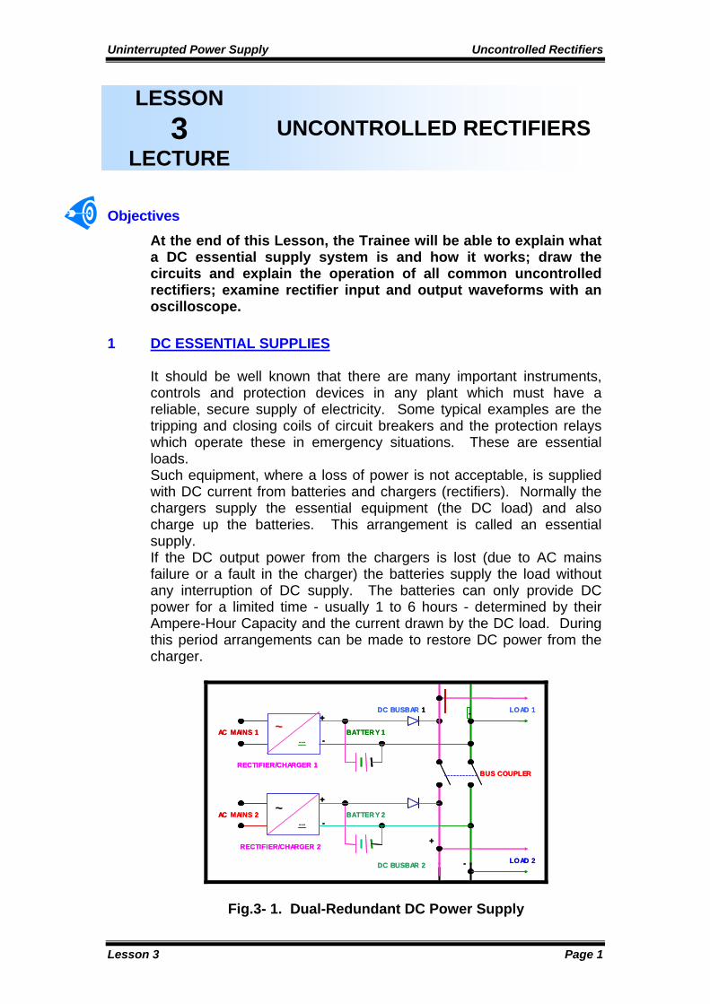
It should be well known that there are many important instruments, controls and protection devices in any plant which must have a reliable, secure supply of electricity. Some typical examples are the tripping and closing coils of circuit breakers and the protection relays which operate these in emergency situations. These are essential loads. Such equipment, where a loss of power is not acceptable, is supplied with DC current from batteries and chargers (rectifiers). Normally the chargers supply the essential equipment (the DC load) and also charge up the batteries. This arrangement is called an essential supply. If the DC output power from the chargers is lost (due to AC mains failure or a fault in the charger) the batteries supply the load without any interruption of DC supply. The batteries can only provide DC power for a limited time - usually 1 to 6 hours - determined by their Ampere-Hour Capacity and the current drawn by the DC load. During this period arrangements can be made to restore DC power from the charger.
~
~
---
---
AC MAINS 1
AC MAINS 2
RECTIFIER/CHARGER 1
RECTIFIER/CHARGER 2
BATTER Y 1
BATTER Y 2
-
+
-
DC BUSBAR 1
DC BUSBAR 2
LOAD 1
LOAD 2
+
+
-
-
BUS COUPLER
~
~
---
---
AC MAINS 1
AC MAINS 2
RECTIFIER/CHARGER 1
RECTIFIER/CHARGER 2
BATTER Y 1
BATTER Y 2
-
+
-
DC BUSBAR 1
DC BUSBAR 2
LOAD 1
LOAD 2
+
+
-
-
BUS COUPLER
Fig.3- 1. Dual-Redundant DC Power Supply

Uninterrupted Power Supply Uncontrolled Rectifiers
Lesson 3 Page 2
Fig.3--1 shows a common DC supply system. It is called Dual Redundant because either of the two power lines can be lost without affecting the loads. Each battery bank has the capacity to supply all DC loads. Besides providing secure DC supplies during emergencies, this scheme also allows one DC supply line to be taken out for maintenance without shutting the DC system down. There are two blocking diodes to prevent a healthy DC supply backfeeding into a faulty one. The bus coupler (usually a circuit breaker) is normally closed, but can be opened for maintenance of either busbar. Further flexibility can be obtained by providing facilities for switching each load to either busbar. There are two classes of rectifier which can be used in DC systems: 1. Controlled Rectifiers, which use Silicon Controlled Rectifiers (SCRs) as the rectifying element. 2. Uncontrolled Rectifiers, which use Diodes as the rectifying element. In this lesson we will examine the Uncontrolled Rectifier. The trainee should already be familiar with basic rectifier circuits, but they are reviewed here in order to lead on to filters and controlled rectifiers.
2 HALF WAVE RECTIFIER
A Half Wave Rectifier is basically one diode supplied by a transformer (Fig.3--2).
LOAD
TX
D
Eout
I
Ein
(DC)
(AC) LOAD
TX
D
Eout
I
Ein
(DC)
(AC)
Fig.3- 2. Half Wave Rectifier Circuit The transformer (TX) steps the AC voltage down to the level needed by the DC load and isolates the DC circuit from the AC supply. The diode only conducts for positive half cycles of the mains AC, when it is forward biased (top of circuit is positive). When the mains AC is negative the diode is reverse biased, so no current can flow. So this circuit only allows the positive half cycles to pass to the load.
-E
t
SINUSOIDAL A.C.
t
-E
-E
+E
PULSATING D.C.HALF WAVE RECTIFIED
Epeak EpeakE ave
-E
t
SINUSOIDAL A.C.
t
-E
-E
+E
PULSATING D.C.HALF WAVE RECTIFIED
Epeak EpeakE ave
Fig.3-3. Waveforms

Uninterrupted Power Supply Uncontrolled Rectifiers
Lesson 3 Page 3
Eout and I are half wave pulsating DC as shown in Fig.3--3. The Average Value of Eout is given by: Eave = Epeak ≈ 0.318 x Epeak π Eave is the effective DC voltage produced by the rectifier - the voltage measured by a DC voltmeter. The Half Wave Rectifier is therefore not a very useful circuit, as Eave is less than a third of the peak value. During negative half cycles of the AC input, when it is not conducting, the diode can have full peak AC voltage across it. So its PRV (Peak Reverse Voltage Rating) must be higher than Epeak. The peak value of the pulsating DC output voltage is smaller than that of the AC input because of the Forward Drop (VF) across the diode. Usually this difference (0.7 V for a silicon diode) is negligible, but has a large effect in low voltage (small power) rectifiers.
3 FULL WAVE RECTIFIERS 3.1 CENTRE-TAP TRANSFORMER RECTIFIER Refer to Fig.3-4:
TX
Ein (AC)
D1
D2
Eout
LOAD
TX
Ein (AC)
D1
D2
Eout
LOAD
Fig.3- 4. Centre-Tap Rectifier Circuit The transformer is now centre-tapped and there are two diodes. When the mains AC voltage is positive, D1 is Forward Biased and conducts current to the Load. D2 is Reverse Biased and does not conduct. When the mains AC voltage is negative, D1 is Reverse Biased and does not conduct. D2 is Forward Biased and conducts current. Current flows in the same direction through the load all the time. out is therefore Full Wave pulsating DC as shown in Fig.3- 5 :

Uninterrupted Power Supply Uncontrolled Rectifiers
Lesson 3 Page 4
t
SINUSOIDAL A.C.
t
PULSATING D.C.
+Ein
-Ein
+Eout
-EoutFULL WAVE RECTIFIED
AVERAGE VALUE
t
SINUSOIDAL A.C.
t
PULSATING D.C.
+Ein
-Ein
+Eout
-EoutFULL WAVE RECTIFIED
AVERAGE VALUE
Fig.3- 5. Waveforms The Average Value of Eout is given by: Eave = 2 x Epeak_ ≈ 0.636 x Epeak π Because Eave is twice as large, this is a better rectifier circuit than the Half Wave type. However, it has two disadvantages: 1. A centre-tap transformer is needed but only one of the two windings is used at any time. This is wasteful. 2. The two diodes must have a PRV rating of twice the peak DC output voltage, because the whole transformer secondary voltage is applied across them in reverse bias. So this circuit is not efficient in terms of materials needed. 3.2 BRIDGE RECTIFIER Refer to Fig.3--6 on the next page.The transformer is not centre-tapped and there are now four diodes. When the transformer AC supply is positive, D1 and D2 are Forward Biased, allowing current through the Load. D3 and D4 are Reverse Biased and do not conduct. When the transformer AC supply is negative, D1 and D2 are Reverse Biased and do not conduct. D3 and D4 are Forward Biased, allowing current through the Load.
TX
E in (AC)
D2
LOAD
D1
D3
D4
EOUT
TX
E in (AC)
D2
LOAD
D1
D3
D4
EOUT
Fig.3- 6. Bridge Rectifier Circuit

Uninterrupted Power Supply Uncontrolled Rectifiers
Lesson 3 Page 5
Pulsating DC current flows the same way through the load all the time. So we have a Full Wave Rectifier again. This is the best rectifier circuit, as it produces the same Average DC output voltage as the Centre-Tap circuit, but uses a single-winding transformer. Also, the PRV of the four diodes does not have to be twice the DC peak output voltage. The circuit can be re-drawn as in Fig.3-7:
TX
Ein
(AC)D2
LOAD
D1 D3
D4
EOUT
TX
Ein
(AC)D2
LOAD
D1 D3
D4
EOUT
Fig.3- 7. Bridge Rectifier Circuit The trainee should be able to verify this is the same circuit as that in Fig.3- 6. It has simply been re-drawn to clearly show the output terminals at the right hand side.
4 THREE PHASE BRIDGE RECTIFIER 4.1 RECTIFIER CIRCUIT Three phase rectifiers can deliver more power than single phase units and produce a much smoother DC output, because the output voltage is the average of three full-wave waveforms of pulsating DC. So for DC systems with large loads, three phase bridge rectifiers are commonly used. Fig.3-8 shows a typical three phase rectifier:
Fig.3- 8. Three-Phase Bridge Rectifier

Uninterrupted Power Supply Uncontrolled Rectifiers
Lesson 3 Page 6
The fuses in series with the diodes prevent damage to the circuit if a diode breaks down (becomes a short circuit) due to excessive reverse bias voltage. They can also protect the diodes from excess current caused by overloads or faults. Three voltages are applied in parallel across the Load by the AC input transformer - EAB, EBC and ECA. Due to the rectifying action of the diodes, these three voltages are full wave rectified pulsating DC at the load. The trainee should confirm that: 1. Positive half cycles of EAB are rectified by diodes D1A and D2B, while negative half cycles are rectified by diodes D1B and D2A. 2. Positive half cycles of EBC are rectified by diodes D1B and D2C, while negative half cycles are rectified by diodes D1C and D2B. 3. Positive half cycles of ECA are rectified by diodes D1C and D2A, while negative half cycles are rectified by diodes D1A and D2C. Fig.3--9 shows the waveforms of these three pulsating DC voltages:
TIME
Epeak
+ VOLTS
EAB EBC ECA
Fig.3- 9. Pulsating DC Waveforms Fig.3--10 shows the resulting output voltage waveform across the load, which is always the largest of the three instantaneous voltages:
IF
Epeak
TIME
Emin
Fig.3- 10. Waveform of Eout

Uninterrupted Power Supply Uncontrolled Rectifiers
Lesson 3 Page 7
The Minimum Value of Eout is 0.866 x Peak Value. The Average Value is 0.94 x Peak Value. So the three-phase bridge rectifier produces a very good DC output voltage with very little ripple. 4.2 PRV AND RIPPLE The PRV rating required by the six diodes is equal to the full phase-to-phase, peak value of the AC input, which equals the peak DC output voltage. Although the DC output voltage from the three-phase rectifier is much better than those from single phase rectifiers, it still contains ripple. So the waveform can be regarded as having two components: 1. Eave - a constant (smooth) DC voltage. 2. Eripple - a ripple waveform which can be approximated to a sawtooth. This is superimposed on the steady DC component. Example: Calculate the % ripple and ripple frequency in the output voltage from a three phase rectifier where the AC supply frequency is 50 Hz.. Answer: Eripple = Epeak - Emin = Epeak - 0.866 x Epeak Eripple = Epeak(1 - 0.866) = 0.134 x Epeak % Ripple = Eripple x 100 = 0.134 x Epeak x 100 Eave 0.94 x Epeak % Ripple = 0.134 x 100 = 14% 0.94 Ripple Frequency is six times the AC supply frequency, as there are six output ripples for each cycle of AC supply. Ripple Frequency = 6 x 50 = 300 Hz
5 PRACTICAL EXERCISE - RECTIFIER WAVEFORMS 5.1 OBJECTIVES 1. To use Experiment Board No. 1 to construct the following circuits: HALF WAVE RECTIFIER FULL WAVE BRIDGE RECTIFIER 2. To examine the circuit output voltage waveform. 5.2 GENERAL PRECAUTIONS Never touch any circuit components or connections unless the circuit is isolated from electrical supply.
Uninterrupted Power Supply Uncontrolled Rectifiers
Lesson 3 Page 8
5.3 SPECIAL PRECAUTIONS WHEN USING AN
OSCILLOSCOPE 1. Always ZERO the channel traces before connecting the probes to a circuit. 2. Measure voltages in DC circuits using the DC display function. 3. Always check the vertical and horizontal gain controls are set to calibrate when measuring voltages or time periods. 4. When using both input channels, always connect the 2 probe ground connections at the same place - otherwise part of the circuit being tested will be shorted out through the CRO. 5.4 EQUIPMENT 1. Experiment Board No. 1. 2. 120 V AC mains supply. 3. Miniature test leads. 4. Oscilloscope. 5.5 PROCEDURE 5.6 Half Wave Rectifier 1. Using CR2 on Experiment Board 1, construct a Half Wave Rectifier. 2. Display the input and output voltage waveforms on the oscilloscope and measure their peak values and their periods. 3. Calculate the average value of the output voltage waveform and its frequency. 4. Use the AC setting of your oscilloscope to measure the average value of the output voltage directly. Then measure the output voltage with a digital multimeter. 5. Use your oscilloscope to measure the peak reverse voltage across the diode. 6. Complete the Results Table and Conclusions section. 5.6 Bridge Rectifier Construct a Bridge Rectifier and repeat steps 1 to 6.

Uninterrupted Power Supply Uncontrolled Rectifiers
Lesson 3 Page 9
5.6 RESULTS TABLE
RECTIFIER
CRO MEASUREMENTS
DIGIT
AL CIRCUIT
AC
DC OUTPUT VOLTAGE
DIODE
METER
RDG INPUT
Epeak
Epeak CALC.Eave
CROEave
PERIOD
FREQ. PRV OUTPUTVOLTS
HALF WAVE
55 V
52 V
16.5 V
16.5 V
16.6 mS
60 Hz
55 V
16.5 V
FULL WAVE
55 V
52 V
33 V
33 V
8.3 mS
120 Hz
55 V
33 V
5.6 CONCLUSIONS 1. Is the output frequency of the Full Wave circuit different to that of the Half Wave circuit? If so, explain why. Answer: YES. BECAUSE THE FULL WAVE CIRCUIT PRODUCES 2 OUTPUT PULSES FOR EVERY CYCLE OF INPUT AC. SO ITS OUTPUT FREQUENCY IS DOUBLE THAT OF THE HALF WAVE RECTIFIER. 2. Is the average output voltage of the Full Wave circuit different to that of the Half Wave circuit? If so, explain why. Answer: YES. BECAUSE THE FULL WAVE CIRCUIT PRODUCES TWICE AS MANY OUTPUT PULSES AS THE HALF WAVE, ITS AVERAGE OUTPUT VOLTAGE IS TWICE AS LARGE. 3. Do your calculated values of average output voltage agree with those measured directly on the oscilloscope and the digital voltmeter readings? If so, explain why. Answer: YES. THE OSCILLOSCOPE SET TO AC WILL SHOW THE AVERAGE VALUE OF VOLTAGE. THE DC VOLTMETER ONLY RESPONDS TO AVERAGE VOLTAGE. SO ALL THREE VALUES SHOULD BE THE SAME. 4. What minimum PRV rating should the diode have: (A) For the Half Wave Rectifier? Answer: 55 V (B) For the Bridge Rectifier? Answer: 55 V

Uninterrupted Power Supply Uncontrolled Rectifiers
Lesson 3 Page 10
5.6 EXERCISE MARKING SCALE 1. Practical Work: Correct Construction - 2 x 5 points = 10 points of two Circuits Correct use of 2-channel - = 10 points CRO and multimeter Sub-Total = 20 points 2. Results Table: 16 correct results - 16 x 3 points = 48 points Sub-Total = 48 points 3. Conclusions: Conclusion 1 - = 8 points Conclusion 2 - = 8 points Conclusion 3 - = 8 points Conclusion 4 - = 8 points Sub-Total = 32 points
OVERALL TOTAL = 100 Points

Uninterrupted Power Supply Dc Filters
Lesson 4 Page 1
LESSON 4
LECTURE DC FILTERS
Objectives
At the end of this Lesson, the Trainee will be able to identify the common DC filter circuits and explain how a capacitor and inductor operate as filters.
1 SHUNT CAPACITOR FILTER
A capacitor can store charge. So if a capacitor is placed as a shunt across the load in a Rectifier circuit, it will do two things: 1. Charge up when positive pulses of rectified current are supplied by the rectifier. 2. Discharge through the load when the rectifier is not conducting. So a shunt capacitor smoothes the ripple (pulses) and raises the average voltage of the rectifier output, giving a much smoother (filtered) DC output. 1.1 FILTER ACTION Fig. 4-1 shows the current flow for a half wave rectifier with a shunt capacitor filter during conduction of the rectifying diode. There are two currents, one to supply the load and one to charge up the capacitor.
LOAD
TX
D
Eout
I
Ein
(AC)
L
I C
+
-
SHUNT
CAPACITOR
LOAD
TX
D
Eout
I
Ein
(AC)
L
I C
+
-
SHUNT
CAPACITOR
Fig. 4-1. Shunt Capacitor being Charged Fig. 4-2 on the next page shows the current flow for the same circuit during blocking by the rectifying diode. Now there is no supply from the transformer, but the shunt capacitor discharges through the load, maintaining its voltage and current:

Uninterrupted Power Supply Dc Filters
Lesson 4 Page 2
LOAD
TX
D
Eout
I
Ein(AC)
C
I C
+
-
SHUNTCAPACITOR
Fig. 4-2. Capacitor Discharging through the Load 1.2 WAVEFORM AND RIPPLE Refer to Fig. 4-3 to see the effect of shunt capacitance on the load:
t
SINUSOIDAL A.C.
t
FILTERED D.C.
+Ein
-Ein
+Eout
-Eout
DISCHARGECAPACITORCAPACITOR
CHARGE
Fig. 4-3. Effect of Capacitor on the Load So the shunt capacitor has smoothed the pulsating DC waveform. The larger the capacitance used, the better the smoothing. So a large capacitor will provide perfectly smooth DC. Because large capacitors are needed for filtering and the rectifier output is never negative, electrolytic capacitors are usually used in filter circuits. The capacitor filter has converted pulsating DC voltage to filtered DC, which contains some ripple (refer to Lesson 1 - Three Phase Bridge Rectifier). Normally a ripple factor of 10% is acceptable. If less ripple is desired, a larger electrolytic capacitor must be used. So we need to be able to calculate the required capacitance: Peak-to-Peak value of the ripple waveform = Eripple Eripple = Epeak - Emin and Eripple =2(Epeak - Eave) Eave = Average Value of Output Voltage (DC value) % Ripple = Eripple x 100 = (Epeak - Emin) x 100 Eave Eave

Uninterrupted Power Supply Dc Filters
Lesson 4 Page 3
It can also be shown that: Eripple = _ I _ where I is the DC Load Current, f is the ripple f x C frequency and C is the filter capacitance. So: % Ripple = ____I x 100 f x C x Eave Example: A Bridge Rectifier, supplied with 60 Hz AC, and capacitor filter must supply an average DC voltage of 17.8 V to a resistive load of 1.78 kΩ with a maximum ripple of 1%. Calculate: (A)Peak-to-Peak value of the ripple voltage. (B)The value of filter capacitor required. Answer: (A)% Ripple = Eripple x 100 Eave Eripple = % Ripple x Eave 100 Eripple = 1 x 17.8 = 0.178 V 100 (B)I = Eave = __17.8___ = 10 x 10-3 A Rload 1.78 x 10³ Since the rectifier is a Full Wave Bridge, the ripple frequency is double the AC supply frequency: f = 2 x 60 = 120 Hz Eripple = _ I _ f x C C = ___I___ = _10 x 10-3_ = 0.47 x 10⁻³ F f x Eripple 120 x 0.178 C = 470 µF
2 PRV RATINGS The filter capacitor can have a large effect on the PRV ratings of the rectifying diodes, because it keeps the cathodes positive when the AC supply is in its negative half cycle.

Uninterrupted Power Supply Dc Filters
Lesson 4 Page 4
2.1 FILTERED HALF-WAVE RECTIFIER Refer to the circuit in Fig. 4-4:
- Epeak + Epeak
C
PRV
Fig. 4-4. Effect of Filter on PRV Without the filter capacitor, the PRV of the diode needs only to be greater than Epeak to avoid damage during negative half cycles of the AC supply. But with a filter capacitor, an extra voltage (+Epeak) is applied to the cathode of the diode. So: PRV = 2 x Epeak So the diode must have a PRV at least equal to two times the peak AC supply voltage. 2.2 FILTERED FULL-WAVE RECTIFIERS The trainee should be able to prove that both the Bridge and Centre-Tap full wave rectifiers are unaffected by the filter capacitor, since the capacitor acts in parallel with the negative half cycle of AC supply. Remember that in the Centre-Tap Rectifier the PRV required is at least equal to two times the peak output DC voltage. This is the same as one times the peak input AC voltage, because of the transformer centre tap. For the Bridge Rectifier, the PRV ratings, peak input AC voltage and peak output DC voltage are all the same. 2.3 PRACTICAL DEMONSTRATION The instructor will demonstrate the effect of a shunt capacitor filter on a Bridge Rectifier using Experiment Board 1 and an oscilloscope.
3 OTHER TYPES OF FILTER 3.1 SERIES INDUCTOR FILTER An inductor stores energy in its magnetic field. When the current flowing through the inductor changes, this stored energy is released

Uninterrupted Power Supply Dc Filters
Lesson 4 Page 5
and tries to keep the current constant. A series inductor can therefore be used as a filter, as in Fig. 4-5.
LOAD
TX
D
Eout
I
Ein (AC)
L+
-
SERIESINDUCTOR
Fig. 4-5. Series Inductor Filter Unlike the shunt capacitor, which basically works upon the output voltage, helping to raise its average value, the series inductor works upon the output current, trying to keep it constant at its average value. This filter does nothing to improve the average DC output voltage from the rectifier. But it can smooth out the waveform and can compensate for large changes in load current, which would severely reduce the average output voltage from a shunt capacitor filter. Fig. 4-6 shows the effect of a series inductor filter on the rectifier output:
t t
+E +E
BRIDGE OUTPUT TO
INDUCTIVE OUTPUT TO
AVERAG AVERAG
Fig. 4-6. Inductive Filter Waveforms 3.2 PI FILTER The shunt capacitor is excellent for smoothing and raising the average value of the output voltage from a rectifier, but can be ineffective for control of large, rapidly changing output currents. The series inductor is excellent for smoothing large currents, but does not raise the average DC voltage. So these two devices are often used together in a PI (π) Filter. A PI Filter is shown connected to the output of a Half Wave Rectifier in Fig. 7-2-7 on the next page. The first capacitor filters and raises the average DC output voltage. The inductor filters again and provides control of large changing currents. The second capacitor provides the final stage of filtering.

Uninterrupted Power Supply Dc Filters
Lesson 4 Page 6
LOAD
TX
D
Eout
I
Ein (AC)
L+
-
Fig. 4-7. PI Filter
Often only one capacitor is needed. In this case the circuit is called an L-Filter because of its shape.

UNINTERRUPTED POWER SUPPLY VOLTAGE REGULATORS
Lesson 5 Page 1
LESSON 5
LECTURE VOLTAGE REGULATORS
Objectives
At the end of this Lesson, the Trainee will be able to identify the common voltage regulator circuits and describe how they work.
1 ZENER SERIES REGULATOR
When the output voltage from an uncontrolled rectifier is applied to a load, it will decrease as the load current increases and increase as the load current decreases. This is because of changes in the circuit losses
Rs
+
-
Vcc(input voltage)
EoutRL
VZV
BE
I s I L
I z
I B
Fig. 5-1. Zener Follower Circuit Therefore Q conducts for shorter periods and Eou Also, fluctuations in the AC supply voltage will affect the DC output voltage from the rectifier, as will ripple. So we need a voltage regulator to maintain constant DC voltage. The simple Zener Diode Voltage Regulator described in Common Module 6 is not suitable for regulating large DC power supplies. But it can be adapted. 1.1 ZENER FOLLOWER Refer to Fig. 5-1. This circuit is called a Zener Follower because it uses an Emitter Follower transistor configuration with a Zener Diode. The basic important equations are:

UNINTERRUPTED POWER SUPPLY VOLTAGE REGULATORS
Lesson 5 Page 2
Eout = VZ - VBE and IB = IL β . (β is the current gain of the transistor amplifier) The advantage of this circuit over the simple Zener Diode Regulator is that a small Base current controls a large load current. Since the Base current is set by the Zener diode, a low power Zener can control large load currents. Without the transistor, the Zener diode would need to handle very large currents directly. This entails very high power rating and large heat sinks. Example 1: VCC = 20 V, VZ = 10 V, β = 80, RS = 680 Ω, RL = 15 Ω. Find IZ. Answer: IS = ( VCC - VZ) = (20 - 10) = 0.0147 A RS 680 Eout = (VZ - VBE) = (10 - 0.7) = 9.3 V IL = Eout = 9.3 = 0.62 A RL 15 IB = IL = O.62 = 0.00775 A (7.75 mA) β 80 IZ = (IS - IB ) = (14.7 - 7.75) =6.95 mA So a fairly low power Zener diode (drawing 7 mA) can regulate the voltage in a load circuit with nearly 100 times as much current flowing (620 mA). Example 2: Re-calculate IZ if VZ = 15 V and RS = 330 Ω. Answer: IS = ( VCC - VZ) = (20 - 15) = 0.01515 A RS 330 Eout = (VZ - VBE) = (15 - 0.7) = 14.3 V IL = Eout = 14.3 = 0.95 A RL 15 IB = IL = O.95 = 0.01187 A (11.87 mA) β 80 IZ = (IS - IB ) = (15.15 - 11.87) =3.28 mA Note that to obtain a higher output voltage we have to use a larger VZ. This means using a smaller RS, otherwise there will not be enough Base current to turn on the transistor.

UNINTERRUPTED POWER SUPPLY VOLTAGE REGULATORS
Lesson 5 Page 3
1.2 NEGATIVE FEEDBACK
Rs
+
-
Vcc(input
Eout
voltage)
R3
RL
R1
R2
Q2
Q1
VFVZ
Fig. 5-2. Voltage Feedback Regulator Circuit
The circuit in Fig. 5-2 is a refinement of the Zener Follower using an extra transistor to provide a Negative Voltage Feedback Signal. Negative Feedback is commonly used in electronics and instrumentation as a means of fixing the output by controlling the input. Although it may not be obvious, this is the same circuit as FIG. 5-1 with some simple additions: Between Q2 and the Zener diode an extra transistor has been placed. This is the Feedback Transistor (Q1). Q1 has a collector resistance R3, and receives its feedback bias (VF) from adjustable voltage divider R1 and R2. All load current passes through Q2, the Emitter Follower transistor. Q1 is a Common Emitter transistor whose biasing is set by the feedback voltage. The larger VF is, the more collector current flows through Q1 and the Zener diode. So as Eout rises, so does VF and the current through Q1 via R3. This diverts some current away from the Base of Q2, so the load current and Eout will reduce. If Eout reduces the reverse happens and Eout will be forced to rise back to its original level. This circuit therefore uses negative feedback to automatically compensate for both load and supply voltage changes. The desired level of output voltage is set by the potentiometer section of voltage divider R1 and R2. 1.3 CURRENT LIMITING The series voltage regulator has one major defect. If the output terminals are short circuited (or overloaded) the pass transistor (Q2) will be destroyed by excessive heat caused by the very large load current .
UNINTERRUPTED POWER SUPPLY VOLTAGE REGULATORS
Lesson 5 Page 4
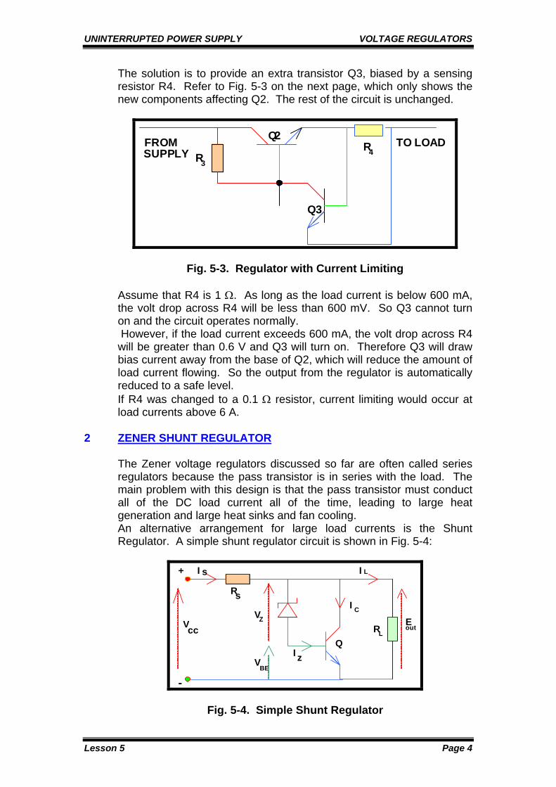
The solution is to provide an extra transistor Q3, biased by a sensing resistor R4. Refer to Fig. 5-3 on the next page, which only shows the new components affecting Q2. The rest of the circuit is unchanged.
R3
Q2
Q3
R4FROMSUPPLY
TO LOAD
Fig. 5-3. Regulator with Current Limiting
Assume that R4 is 1 Ω. As long as the load current is below 600 mA, the volt drop across R4 will be less than 600 mV. So Q3 cannot turn on and the circuit operates normally. However, if the load current exceeds 600 mA, the volt drop across R4 will be greater than 0.6 V and Q3 will turn on. Therefore Q3 will draw bias current away from the base of Q2, which will reduce the amount of load current flowing. So the output from the regulator is automatically reduced to a safe level. If R4 was changed to a 0.1 Ω resistor, current limiting would occur at load currents above 6 A.
2 ZENER SHUNT REGULATOR The Zener voltage regulators discussed so far are often called series regulators because the pass transistor is in series with the load. The main problem with this design is that the pass transistor must conduct all of the DC load current all of the time, leading to large heat generation and large heat sinks and fan cooling. An alternative arrangement for large load currents is the Shunt Regulator. A simple shunt regulator circuit is shown in Fig. 5-4:
Rs
+
-
VccEoutRL
VZ
VBE
I s I L
I zQ
I C
Fig. 5-4. Simple Shunt Regulator

UNINTERRUPTED POWER SUPPLY VOLTAGE REGULATORS
Lesson 5 Page 5
The bias voltage for the shunt transistor is held constant by the Zener diode. If the input voltage rises, more current flows through the Zener. So the shunt transistor has a larger base current and therefore a larger collector current. The result is that the shunt transistor diverts excess current and the load current and load voltage stay constant. If the input voltage reduces, the procedure reverses. If the load itself changes so IL varies, the currents through the Zener and transistor also vary and VCC and Eout are kept constant. As the voltages across the Zener, transistor and load are constant, series resistor RS absorbs the fluctuations of VCC and is short circuit protection. Although the Shunt Regulator is more suitable than the Series Regulator for large load currents, it is does not have such good regulation. For large power DC systems the Switching Regulator is better than either of the Zener regulators.
3 SWITCHING REGULATOR 3.1 BASIC OPERATION Fig. 5-5 shows a simplified circuit of a Switching Regulator:
PULSEGENERATOR
L
CD
Q
LOAD
EE outin
VF
Fig. 5-5. Switching Regulator Circuit The pass transistor (Q) does not conduct all the time - it acts as a fast acting DC switch, biased by the pulse train coming from the Pulse Generator. Q is not continuously conducting, so does not get too hot . The output from Q is also a pulse train, but is much bigger than that supplied to the base of Q. A typical pulse train frequency is 20 kHz. The pulse train is then fed to an LC filter where it is smoothed by the inductor (L) and AC ripple shunted away by the capacitor (C). Because the pulse frequency is so high, a small inductor can be used and a high reactance (good smoothing) achieved. For the same reason, a small capacitor can be used and a low reactance (good shunting of ripple) achieved.

UNINTERRUPTED POWER SUPPLY VOLTAGE REGULATORS
Lesson 5 Page 6
Part of the smooth DC output voltage (Eout) from the regulator is fed back as the input signal (VF) to the pulse generator. This is called negative feedback, since if Eout rises, the output pulses from the pulse generator become narrower. t will reduce. The reverse happens if Eout falls. The diode (D) is a Freewheeling Diode. When the DC supply to any inductor is cut off, its magnetic field tries to maintain constant current by generating a back-emf (inductive kickback). Without the diode to discharge through, the inductor would force current to flow through Q. The large inductive voltage would damage the transistor. 3.2 PULSE GENERATOR Refer to Fig. 5-6. This shows a typical simplified circuit.
+-
+-
+-
+-
.
Eref
COMPARATORR
R
1
2
INTEGRATOR
R3
C2
.
R4
R5
.
R6R7
.OSCILLATOR
TO (Q)
TO LC FILTERE
out
VF
PULSE CONVERTER
C3
Fig. 5-6. Pulse Generator Circuit The oscillator produces a square wave whose frequency is set by R5 and C3. The integrator converts this square wave to a triangular wave. This signal is supplied to the pulse converter’s non-inverting input. Meanwhile, a feedback voltage (VF) is derived from Eout by the voltage divider R1 and R2. VF is taken to the comparator. Here it is compared with a reference voltage (Eref) which is usually taken from a Zener diode. The difference between VF and Eref is the error, which can be positive or negative. This is applied to the inverting input of the pulse converter, which converts the triangular waveform to a pulse train. Control of the width of the pulses is done by the error input to the Comparator. If Eout rises: The comparator produces a larger positive output voltage. This error signal is inverted in the pulse converter and reduces the width of the output pulses. So Q conducts for less time and Eout is reduced back

UNINTERRUPTED POWER SUPPLY VOLTAGE REGULATORS
Lesson 5 Page 7
to normal. If Eout decreases, the procedure reverses to raise it back to normal. Example: R1 = 3 kΩ, R2 = 1 kΩ, Eref = 1.25 VDC. What should Eout be? Answer: Current in R1 and R2 = Eref = __Eout __ R2 (R1 + R2) Eout = Eref (R1 + R2) = 1.25 x (3 + 1) x 103 R2 1 x 10³ Eout = 5 VDC The output voltage will be constant 5 VDC as long as Eref is 1.25 VDC.
4 OPERATIONAL AMPLIFIER The Operational Amplifier (Op-Amp) is an Integrated Circuit (IC). This is a complete electronic circuit (resistors, diodes and transistors) manufactured on one small silicon chip. The Op-Amp is much smaller and cheaper than a circuit assembled from individual components. It gets its name from the many different electronic operations it can do (amplifier, oscillator, waveshaper and voltage regulator to name only a few). 4.1 BASIC 741C OP-AMP Refer to Fig. 5-7:
741
1 2 3 4 5 6 7
891011121314
IC OP-
TOP
SIDE
1 2 3 4PIN
1 2 3 4
5678
Fig. 5-7. 741C Package The Op-Amp has 8 pins (terminals) arranged in two parallel rows of 4. So its package is called 8/DIL (8 pin, dual-in-line). In the example shown, the chip is installed in a 14-pin IC socket. The pins (terminals) are numbered in a specific sequence - 1 to 8 from the bottom left hand side. The type number 741C tells you this is an industry-standard, general purpose Op-Amp. There are also many special-application Op-Amps. Each type has a different type number.

UNINTERRUPTED POWER SUPPLY VOLTAGE REGULATORS
Lesson 5 Page 8
Some may be of 14/DIL construction and others may have TO (transistor-type) packages. The circuit symbol for an Op-Amp is shown in Fig. 5-8:
-
+
2
3
1 54
6
7
Fig. 5-8. OP-AMP Symbol The three terminals of major interest are 2, 3 and 6: - Terminal 2 is the Inverting Input. - Terminal 3 is the Non-Inverting Input. - Terminal 6 is the Output. The Inverting Input converts a positive signal to negative and vice-versa. The Non-Inverting Input does not change the signal polarity. The amplifier’s output is proportional to the Error (Differential) Input - the difference between the Inverting and Non-Inverting Inputs. Terminal 8 is not used. The other four terminals are needed to power and balance the Op-Amp: - Terminals 1 and 5 are for the DC Offset Voltage. - Terminal 7 is the Power Supply Positive. - Terminal 4 is the Power Supply Negative. Terminals 1 and 5 are supplied from the power supply via an external potentiometer. The purpose is to compensate for DC offset (+ or -) voltage at the output when there is no input signal. This DC offset is caused by slight differences between the transistors in the Op-Amp. The Op-Amp Ground-Line for input and output signals is internally fixed at half the DC power supply voltage across terminals 7 and 4. So if a normal 2-terminal power supply is used it must not be grounded, as part of the Op-Amp circuitry will be shorted out. If a dual power supply is used, the Common (centre) terminal may be grounded and connected to the Op-Amp Ground-Line. The Open-Loop Gain (AOL) of an Op-Amp is given by: AOL = ______Output Voltage (at terminal 6)______ Error Input Voltage (between terminals 2 &3) As the Error Input Voltage is the difference between the Inverting and Non-Inverting Inputs, AOL is also called the Differential Gain. Typically, this is approximately 100,000 for a 741C Op-Amp.
UNINTERRUPTED POWER SUPPLY VOLTAGE REGULATORS
Lesson 5 Page 9
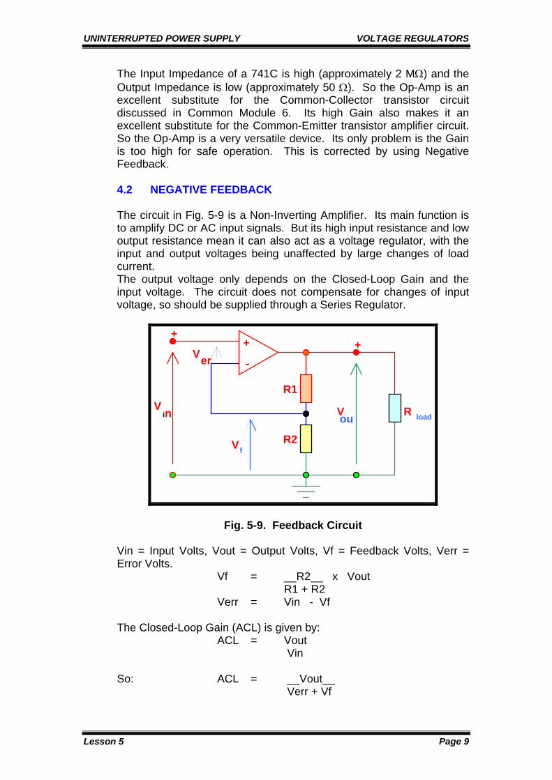
The Input Impedance of a 741C is high (approximately 2 MΩ) and the Output Impedance is low (approximately 50 Ω). So the Op-Amp is an excellent substitute for the Common-Collector transistor circuit discussed in Common Module 6. Its high Gain also makes it an excellent substitute for the Common-Emitter transistor amplifier circuit. So the Op-Amp is a very versatile device. Its only problem is the Gain is too high for safe operation. This is corrected by using Negative Feedback. 4.2 NEGATIVE FEEDBACK The circuit in Fig. 5-9 is a Non-Inverting Amplifier. Its main function is to amplify DC or AC input signals. But its high input resistance and low output resistance mean it can also act as a voltage regulator, with the input and output voltages being unaffected by large changes of load current. The output voltage only depends on the Closed-Loop Gain and the input voltage. The circuit does not compensate for changes of input voltage, so should be supplied through a Series Regulator.
+
-
R1
R2Vf
Vin Vou
Ver
R load
++
Fig. 5-9. Feedback Circuit Vin = Input Volts, Vout = Output Volts, Vf = Feedback Volts, Verr = Error Volts. Vf = __R2__ x Vout R1 + R2 Verr = Vin - Vf The Closed-Loop Gain (ACL) is given by: ACL = Vout Vin So: ACL = __Vout__ Verr + Vf
UNINTERRUPTED POWER SUPPLY VOLTAGE REGULATORS
Lesson 5 Page 10
Since Verr is 100,000 times smaller than Vout it can be ignored: ACL = Vout = Vf(R1 + R2) Vf Vf x R2 ACL = (R1 + R2) = 1 + R1 R2 R2 So, with Negative Feedback, the Gain of this circuit is no longer 100,000 but is always greater than one. The feedback also increases the input impedance to almost infinity and reduces the the output impedance to almost zero. Example 1: R1 = 1 kΩ, R2 = 1 kΩ, Vin = +2 VDC. Calculate: ACL, Vout, Vf and Verr. Answer: ACL = 1 + R1 = 1 + 1 kΩ = 2.0 R2 1 kΩ Vout = ACL x Vin = 2 x 2 = 4.0 VDC Vf = Vout x ___R2___ = _4 x 1 kΩ_ = 2.0 VDC (R1 + R2) (1 kΩ + 1 kΩ) Verr = (Vin - Vf) = (2 - 2) = ZERO In fact, the Error Voltage is not zero, but it is very small: Verr = Vout = __4___ = 40 µV AOL 100,000 Example 2: Recalculate Example 1 if R2 = 10 kΩ. Answer: ACL = 1 + R1 = 1 + 1 kΩ = 1.1 R2 10 kΩ Vout = ACL x Vin = 1.1 x 2 = 2.2 VDC Vf = Vout x __R2__ = _2.2 x 10 kΩ_ = 2.0 VDC (R1 + R2) (1 kΩ + 10 kΩ) Verr = (Vin - Vf) = (2 - 2) = ZERO In fact, the Error Voltage is not zero, but it is very small: Verr = Vout = __2.2__ = 22 µV AOL 100,000

UNINTERRUPTED POWER SUPPLY VOLTAGE REGULATORS
Lesson 5 Page 11
The Instructor will now give a practical demonstration to prove the above calculations, using Experiment Board No. 5 and a 40 VDC power supply. Note that the DC Input voltage is taken from a 0-1 kΩ potentiometer connected between the Positive and Common terminals of the DC power supply. If the potentiometer were connected between the Positive and Negative terminals, there would be a dangerous short-circuit! During the demonstration, observe that as the load resistance (0-10 kΩ potentiometer) at the Op-Amp output is varied from zero to 10 kΩ, the Input and Output Voltages remain constant! This why the Op-Amp is so useful as an Output Voltage Regulator. This is only one application of the Op-Amp. By adding external combinations of resistors and capacitors to the external circuit, we can produce practically any electronic device - integrator, differentiator, pulse generator, oscillator and high-gain AC amplifier to name but a few. 4.3 LM340 VOLTAGE REGULATOR There are integrated circuit devices specially made as DC voltage regulators which can regulate the output DC voltage even though both the load current and input voltage are varying. These devices include elements from the Series Regulator (Zener Follower) with a 741C Op-Amp. They only have three external terminals, which makes installation and testing simple. One common type of DC Voltage Regulator using Op-Amps is the LM340 series. Refer to Fig. 5-10 on the next page. A built-in Reference Voltage circuit (zener diode) supplies the Non-Inverting Input of the Op-Amp. The zener diode takes its supply from Vin. Output voltage feedback supplies the Inverting Input via a built-in voltage divider. The Reference Voltage is set slightly higher than the Feedback Voltage to ensure the Op-Amp output is always positive. If Vout reduces for any reason, the error at the Op-Amp input increases and the Op-Amp increases its output voltage. This increases the bias on the Base of the Pass Transistor, reducing its VCE volt-drop. So Vout increases back to its original level.
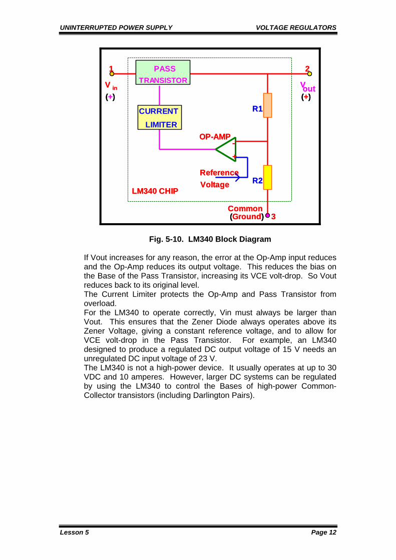
UNINTERRUPTED POWER SUPPLY VOLTAGE REGULATORS
Lesson 5 Page 12
-+
LIMITER
LM340 CHIP
PASSTRANSISTOR
ReferenceVoltage
1 2
3
V in(+)
Vout(+)
Common(Ground)
OP-AMP
R1
R2
CURRENT
-+
LIMITER
LM340 CHIP
PASSTRANSISTOR
ReferenceVoltage
1 2
3
V in(+)
Vout(+)
Common(Ground)
OP-AMP
R1
R2
CURRENT
Fig. 5-10. LM340 Block Diagram If Vout increases for any reason, the error at the Op-Amp input reduces and the Op-Amp reduces its output voltage. This reduces the bias on the Base of the Pass Transistor, increasing its VCE volt-drop. So Vout reduces back to its original level. The Current Limiter protects the Op-Amp and Pass Transistor from overload. For the LM340 to operate correctly, Vin must always be larger than Vout. This ensures that the Zener Diode always operates above its Zener Voltage, giving a constant reference voltage, and to allow for VCE volt-drop in the Pass Transistor. For example, an LM340 designed to produce a regulated DC output voltage of 15 V needs an unregulated DC input voltage of 23 V. The LM340 is not a high-power device. It usually operates at up to 30 VDC and 10 amperes. However, larger DC systems can be regulated by using the LM340 to control the Bases of high-power Common-Collector transistors (including Darlington Pairs).
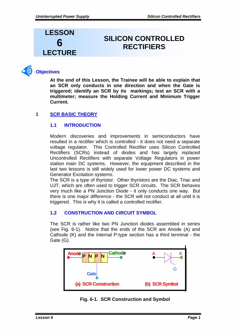
Uninterrupted Power Supply Silicon Controlled Rectifiers
Lesson 6 Page 1
LESSON 6
LECTURE
SILICON CONTROLLED RECTIFIERS
Objectives
At the end of this Lesson, the Trainee will be able to explain that an SCR only conducts in one direction and when the Gate is triggered; identify an SCR by its markings; test an SCR with a multimeter; measure the Holding Current and Minimum Trigger Current.
1 SCR BASIC THEORY 1.1 INTRODUCTION Modern discoveries and improvements in semiconductors have resulted in a rectifier which is controlled - it does not need a separate voltage regulator. This Controlled Rectifier uses Silicon Controlled Rectifiers (SCRs) instead of diodes and has largely replaced Uncontrolled Rectifiers with separate Voltage Regulators in power station main DC systems. However, the equipment described in the last two lessons is still widely used for lower power DC systems and Generator Excitation systems. The SCR is a type of thyristor. Other thyristors are the Diac, Triac and UJT, which are often used to trigger SCR circuits. The SCR behaves very much like a PN Junction Diode - it only conducts one way. But there is one major difference - the SCR will not conduct at all until it is triggered. This is why it is called a controlled rectifier. 1.2 CONSTRUCTION AND CIRCUIT SYMBOL The SCR is rather like two PN Junction diodes assembled in series (see Fig. 6-1). Notice that the ends of the SCR are Anode (A) and Cathode (K) and the internal P-type section has a third terminal - the Gate (G).
N PP NAnode Cathode
Gate
A K
G
(a) SCR Construction (b) SCR Symbol
Fig. 6-1. SCR Construction and Symbol

Uninterrupted Power Supply Silicon Controlled Rectifiers
Lesson 6 Page 2
The SCR is basically a 3-terminal semiconductor switch, which will not turn on (close) until two things happen: 1. The Anode must be positive compared to the Cathode. 2. A positive trigger pulse must be applied to the Gate. It is only necessary to apply a short pulse of Gate current, called a Trigger Pulse. Once this pulse is received, the SCR will conduct until the current flowing from Anode to Cathode is below the Holding Current. Then the SCR switches off. When the applied voltage becomes positive again, another positive trigger pulse is needed to turn on the SCR again. Also shown in Fig. 6-1 is the circuit symbol for an SCR, which is similar to that of a diode. 1.3 SCR OPERATION The equivalent circuit for an SCR is shown in Fig. 6-2:
A +
Q1
Q2G+
-K
I C1 (IB2)
IB1 (IC2
)
Fig. 6-2. SCR Equivalent Circuit (A) must be positive and (K) negative. When a positive pulse is applied to (G), Q2 turns on because it now has forward bias on its Base-Emitter junction. So Collector current (IC2) flows through Q2. But IC2 is also IB1 (the Base Biasing current for PNP transistor Q1). So Q1 turns on and Collector current IC1 flows through it. IC1 is also the Base current for Q2. So Q1 and Q2 keep each other conducting after the Gate pulse has finished. Current can therefore keep flowing from Anode to Cathode. The circuit only stops conducting if one of two things happen: 1. The forward current drops below the Holding Current level (there is not enough Base current to keep the transistors forward biased). 2. The supply polarity reverses (as with an AC supply). In this case the transistors are reverse biased and they turn off.

Uninterrupted Power Supply Silicon Controlled Rectifiers
Lesson 6 Page 3
The trainee should be able to prove that the current flowing into the SCR from (A) equals the current leaving the SCR at (K) and they are equal to: (IC1 + IC2) 1.4 COMPARISON WITH DIODE 1. Advantage of the SCR: Because the SCR conducts when a positive Gate pulse is applied and turns off when the supply to the Anode goes negative, it is an excellent rectifier. The SCR is a more useful rectifier than the diode because the conduction time (and therefore the Average Output Voltage) can be directly controlled by adjusting the timing of the Gate pulses. The voltage regulators discussed in Lesson 2 are therefore not necessary. 2. Disadvantages of the SCR: The SCR is not as robust as a diode, so is much more easily damaged by large reverse voltages and forward currents, especially transients such as sudden load changes, switching surges and short circuit faults at the load. 1.5 RATINGS AND PACKAGES The main SCR ratings are: 1. Maximum Forward Current (IT) - The largest forward bias current the SCR can conduct without overheating and becoming a permanent open circuit. 2. Peak Reverse Voltage (VRRM) - The largest reverse bias voltage the SCR can withstand before breaking down to a permanent short circuit. 3. Maximum Trigger Current (IGT) - The largest Gate current which should trigger the SCR. If an SCR under test needs a higher trigger current than this, it is deteriorating and must be replaced. 4. Maximum Gate Voltage (VGT) - The largest Gate voltage the SCR can withstand without failure. 5. Minimum Holding Current - The minimum forward bias current needed to keep the SCR conducting. An SCR is a 3-terminal device, just like a transistor. Low power SCRs look exactly like transistors, having the same TO package codes. High power SCRs look very like high power diodes, except that they have two pigtails at one end instead of two. If in doubt, check the code number (if any) on the package and consult the manufacturer’s guide. If there is no information available, the SCR must be tested.

Uninterrupted Power Supply Silicon Controlled Rectifiers
Lesson 6 Page 4
2 PRACTICAL EXERCISE - TESTING AN SCR WITH A MULTIMETER 2.1 PRECAUTIONS The same precautions apply as when using multimeters to test components in Common Module 6 - Electronics Workshop. 2.2 PROCEDURE Test the SCR provided using the digital multimeter as a diode tester. Record your readings in the Results Table. 2.3 RESULTS TABLE
(A)TO(G)
+ -
mV
(G)TO (A)
+ -
mV
(A)TO (K)
+ -
mV
(K)TO (A)
+ -
mV
(G)TO(K)
+ -
mV
(K)TO(G)
+ -
mV
∞
∞
∞
∞
800
∞
2.4 CONCLUSIONS 1. Complete the Conclusions Table below:
SCR CONDITION
SCR MATERIAL
HEALTHY
FAULTY
? SILICON
GERM- ANIUM
?
√
√
2. Are the Gate to Cathode test results similar to an ordinary PN junction diode? Explain why. Answer: YES. BECAUSE THE PART OF THE SCR BETWEEN THE GATE AND CATHODE IS A SINGLE PN JUNCTION. 3. Why can you not obtain a low and a high reading when testing between the Anode and Gate? Does this mean the SCR is faulty? Answer: THE PART OF THE SCR BETWEEN THE ANODE AND THE

Uninterrupted Power Supply Silicon Controlled Rectifiers
Lesson 6 Page 5
GATE HAS 2 JUNCTIONS (PNP) SO WILL GIVE 2 INFINITE READINGS. THIS DOES NOT MEAN THE SCR IS FAULTY. 2.5 EXERCISE MARKING SCALE 1. Practical Tests: 6 correct readings - 6 x 5 points = 30 points Sub-Total = 30 points 2. Conclusions: Conclusion Table, - 2 x 15 points = 30 points 2 correct crosses Conclusion 2 - = 20 points Conclusion 3 - = 20 points Sub-Total = 70 points OVERALL TOTAL = 100 Points
3 PRACTICAL EXERCISE - DC TESTS OF AN SCR 3.1 OBJECTIVES 1. To measure the minimum gate current at which an SCR starts to conduct, which should be less than the Maximum Trigger Current rating of the SCR (0.045 mA). 2. To measure the Minimum Holding Current for an SCR which is in conduction mode. 3.2 PRECAUTIONS This experiment involves testing on a live DC circuit. The standard safety precautions apply, especially not touching live components. 3.3 EQUIPMENT “Labvolt” Konnect-All Board SCR, 10 kΩ and 500 kΩ potentiometers Analogue and digital multimeters47 Ω, 4.7 kΩ and 1 kΩ resistors DC power supply unit SPDT switch and PBNO button 3.4 PROCEDURE 1. Construct the circuit shown in Fig. 6-3 on the next page. Set POT to maximum resistance and close SPDT. 2. Slowly reduce POT while pressing PBNO. Eventually a point is reached where A-K current flows and the voltmeter reading changes. Record the meter readings just before and after this point. Complete the Results Table.
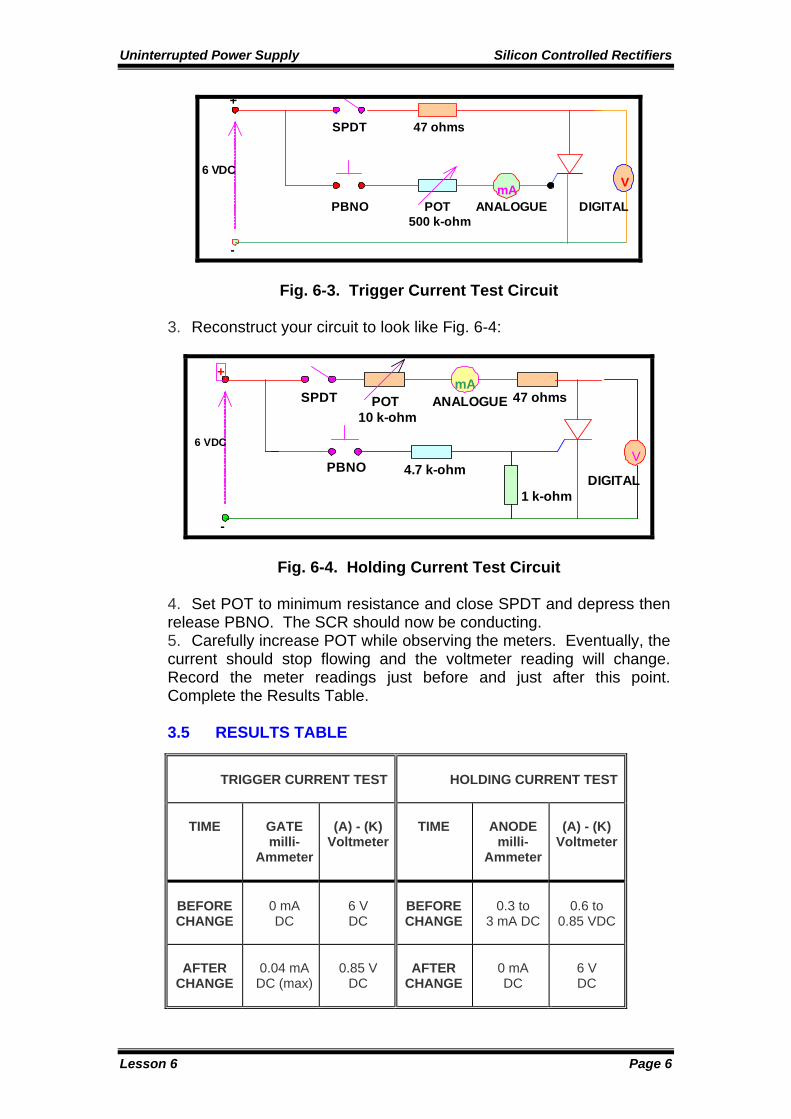
Uninterrupted Power Supply Silicon Controlled Rectifiers
Lesson 6 Page 6
SPDT
PBNO POTmA
ANALOGUE
47 ohms
V
DIGITAL
6 VDC
+
-
500 k-ohm
Fig. 6-3. Trigger Current Test Circuit 3. Reconstruct your circuit to look like Fig. 6-4:
SPDT
PBNO
POTmA
ANALOGUE 47 ohms
V
DIGITAL
6 VDC
+
-
1 k-ohm
4.7 k-ohm
10 k-ohm
Fig. 6-4. Holding Current Test Circuit 4. Set POT to minimum resistance and close SPDT and depress then release PBNO. The SCR should now be conducting. 5. Carefully increase POT while observing the meters. Eventually, the current should stop flowing and the voltmeter reading will change. Record the meter readings just before and just after this point. Complete the Results Table. 3.5 RESULTS TABLE
TRIGGER CURRENT TEST
HOLDING CURRENT TEST
TIME
GATE milli-
Ammeter
(A) - (K)
Voltmeter
TIME
ANODE
milli- Ammeter
(A) - (K)
Voltmeter
BEFORE CHANGE
0 mA DC
6 V DC
BEFORE CHANGE
0.3 to
3 mA DC
0.6 to
0.85 VDC
AFTER
CHANGE
0.04 mA
DC (max)
0.85 V
DC
AFTER
CHANGE
0 mA DC
6 V DC

Uninterrupted Power Supply Silicon Controlled Rectifiers
Lesson 6 Page 7
3.6 CONCLUSIONS 1. For both tests, does the voltmeter reading change? Explain why!! Answer: YES. WHEN THE SCR IS NOT CONDUCTING IT HAS FULL SUPPLY VOLTAGE (6 VDC) ACROSS IT. WHEN IT CONDUCTS, THE VOLT DROP ACROSS IT IS THE FORWARD DROP (0.6 TO 0.85 V). 2. What is the Holding Current for this SCR? Answer: 0.3 to 3.0 mA DC 3. What is the minimum Gate current for this SCR? Answer: 0.04 mA DC (or less) 3.7 EXERCISE MARKING SCALE 1. Practical Tests: Correct circuit assembly - 2 x 10 points = 20 points Results Table correct - 8 x 5 points = 40 points Sub-Total = 60 points 2. Conclusions: Conclusion 1 - = 20 points Conclusion 2 - = 10 points Conclusion 3 - = 10 points Sub-Total = 40 points OVERALL TOTAL = 100 Points

Uninterrupted Power Supply Inverters
Lesson 7 Page 1
LESSON 7
LECTURE INVERTERS
Objectives
At the end of this Lesson, the Trainee will be able to explain the importance of an Inverter in a UPS system; identify the symbol for an Inverter; draw the circuits and explain the operation of common Inverters; explain the use of Commutation SCRs and Capacitors and Freewheeling Diodes.
1 AC ESSENTIAL SUPPLIES
There are certain important electrical loads which require AC current instead of DC. These include emergency lighting, control computers and essential pump motors. To supply these AC essential loads during failure of AC mains power, we need batteries and chargers, just as with DC Essential Loads. But we also need an Inverter to convert the DC from the battery and charger to AC for the loads. Refer to Fig. 7 -1:
~
~
---
---
RECTIFIER 1
RECTIFIER 2
BATTERY 1
BATTERY 2
ESSENTIAL
+
+
-
----
~
---
~INVERTER 1
INVERTER 2
L N
~ ~
LOADS
STATIC SWITCH 1
~ ~
STATIC SWITCH 2
BUSBAR
~ ~STATIC SWITCH 3
AC MAINS 3
AC MAINS 2
AC MAINS 1 ~
~
---
---
RECTIFIER 1
RECTIFIER 2
BATTERY 1
BATTERY 2
ESSENTIAL
+
+
-
----
~
---
~INVERTER 1
INVERTER 2
L N
~ ~
LOADS
STATIC SWITCH 1
~ ~
STATIC SWITCH 2
BUSBAR
~ ~STATIC SWITCH 3
AC MAINS 3
AC MAINS 2
AC MAINS 1
Fig. 7 -1. UPS with Dual Redundancy and AC Bypass The example above is a typical UPS system with dual redundancy. If one charger, one battery or one inverter fails, the other UPS circuit can supply all the essential AC loads. For maintenance or emergencies an AC Bypass (AC mains 3) is also provided. The two Inverters convert DC back to AC and the Static Switches isolate faulty supplies from the AC busbars.
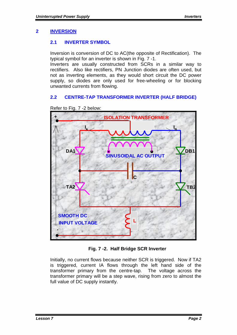
Uninterrupted Power Supply Inverters
Lesson 7 Page 2
2 INVERSION
2.1 INVERTER SYMBOL Inversion is conversion of DC to AC(the opposite of Rectification). The typical symbol for an inverter is shown in Fig. 7 -1. Inverters are usually constructed from SCRs in a similar way to rectifiers. Also like rectifiers, PN Junction diodes are often used, but not as inverting elements, as they would short circuit the DC power supply, so diodes are only used for free-wheeling or for blocking unwanted currents from flowing. 2.2 CENTRE-TAP TRANSFORMER INVERTER (HALF BRIDGE) Refer to Fig. 7 -2 below:
+
SINUSOIDAL AC OUTPUT
C
DA1
TA2
DB1
TB2
ISOLATION TRANSFORMER
I IA B
L
-
SMOOTH DCINPUT VOLTAGE
+
SINUSOIDAL AC OUTPUT
C
DA1
TA2
DB1
TB2
ISOLATION TRANSFORMER
I IA B
L
-
SMOOTH DCINPUT VOLTAGE
Fig. 7 -2. Half Bridge SCR Inverter Initially, no current flows because neither SCR is triggered. Now if TA2 is triggered, current IA flows through the left hand side of the transformer primary from the centre-tap. The voltage across the transformer primary will be a step wave, rising from zero to almost the full value of DC supply instantly.

Uninterrupted Power Supply Inverters
Lesson 7 Page 3
The Commutating Capacitor, C, will charge up because its left side is connected to the DC negative terminal through TA2 and its right side is connected to the DC positive terminal through DB1. After a certain time, TB2 is triggered. C now discharges through TB2 and TA2, helping TB2 to keep conducting and shutting down TA2. Now the right hand side (limb) of the circuit conducts, allowing current IB to flow through the right hand side of the transformer primary from the centre-tap - the reverse of the previous direction (negative instead of positive). Meanwhile, C charges up with reversed polarity. So the voltage across the transformer secondary switches instantly from positive to negative, forming a square waveform. When another trigger pulse is applied to the Gate of TA2, the capacitor C discharges through TA2 and TB2, shutting down TB2 and helping TA2 to conduct. So we have a positive voltage again. The only function of the diodes, DA1 and DA2, is to block the commutating capacitor from discharging through the transformer. The inductor, L, blocks sharp transient currents during switching of the SCRs. The isolating transformer acts as a filter for the square wave voltage, smoothing it to a roughly sinusoidal waveform. The waveforms for this circuit are shown in Fig. 7 -3:
EA
EB(NEGATIV E)
(POSITIV E)
AVERAGEOF EA
& EB
SINUSOIDALOUTP UTVOLT AGEW AVEFORM
TRIGGER TA2TRIGGER TB
180o
Fig. 7 -3. Inverter Waveforms The two SCRs are triggered at 180 degree phase shifts. For a 60 Hz output frequency, this corresponds to a time difference of 8.3 mS: Phase Shift = θ = 180 degrees = π radians

Uninterrupted Power Supply Inverters
Lesson 7 Page 4
θ = 2πft, so t = θ = π = 1 2πf 2πf 2f Since f = 60 Hz, t = 1_ = 0.0083 seconds (8.3 mS) 120 The accurate trigger pulse timing required is usually provided by an oscillator circuit, often incorporating a crystal.
3 FULL BRIDGE INVERTER The simple Half-Bridge Inverter is not flexible enough for use in large UPS systems, where some form of voltage regulation is needed to cater for large fluctuating loads. Also, it does not produce a smooth enough sinusoidal output voltage. So for large UPS systems, the Full Bridge Inverter is used. Refer to Fig. 7 -4:
LOAD
+
-
T1
L1
T2
T3
T4
L4 L2
L3
D1
D4
D3
D2
CA CB
L1A
T1A
T4A
L4A L2A
T2A
T3A
L3A
Fig. 7-4. Full Bridge Inverter T1, T2, T3 and T4 are the Inverting SCRs. CA and CB are the commutating capacitors. D1, D2, D3 and D4 are freewheeling diodes and also assist the commutating capacitors to turn off the inverting SCRs. T1A, T2A, T3A and T4A are blocking SCRs. They operate with CA and CB to turn off T1-T4. 3.1 INVERTING OPERATION To understand the inversion process, the circuit has been simplified by removing the blocking components - see Fig. 7 -5:

Uninterrupted Power Supply Inverters
Lesson 7 Page 5
LOAD
+
-
T1
L1
T2
T3
T4
L4 L2
L3
LOAD
+
-
T1
L1
T2
T3
T4
L4 L2
L3
Fig. 7 -5. Inverting Circuit If T1 and T2 are triggered together, current flows from left to right through the load. When T1 and T2 are turned off and T3 and T4 are turned on, current flows from right to left through the load. The load will receive AC current instead of DC. However, the voltage waveform applied at the load will be more square wave than sinusoidal. This can be corrected by resonant filters (combinations of capacitors and inductors) which remove the harmonics from the square wave, leaving a sinusoidal waveform. The only problem is that we have to find a way to turn the Inverting SCRs off. They will not do this automatically, because the supply to the circuit is smooth DC. 3.2 BLOCKING THE INVERTING SCRS To simplify the explanation, we will only look at one of the Inverting SCRs - T1. The condition when T1 is conducting, and supplying current to the load, is shown in Fig. 7 -6:
LOAD
+T1
L1
D1
CA
L1A
T1A
+- + -I
I
LOAD
+T1
L1
D1
CA
L1A
T1A
+- + -I
I
Fig. 7 -6. T1 Conducting

Uninterrupted Power Supply Inverters
Lesson 7 Page 6
D1 is reverse biased and T1A is not triggered, so they do not conduct. CA charges up because there is a positive supply to the load. To turn off T1, a trigger pulse is first applied to T1A. T1A turning on provides a path for CA to discharge through L1, D1, L1A and T1 as shown in Fig. 7 -7:
LOAD
+T1
L1
D1
CA
L1A
T1A
+- + -
I
ICA
CA
LOAD
+T1
L1
D1
CA
L1A
T1A
+- + -
I
ICA
CA
Fig. 7 -7. CA Discharging The reverse polarity current from the capacitor, ICA, blocks the load current leaving T1. So the current in T1 drops below its Holding Current and T1 turns off. As CA discharges, ICA drops below the Holding Current level for T1A, so T1A turns off. While T1 is being turned off, T2A and CB are performing the same process on T2. So the Inverter Bridge is now ready for trigger pulses to be applied to T3 and T4, to provide a negative half cycle of load current. 3.3 FREEWHEELING AN INDUCTIVE LOAD Essential loads usually contain a lot of inductance (from motors, transformers and solenoids). When the Inverting SCRs are suddenly turned off, this inductance will generate a back-emf to try to keep current flowing. So we need to discharge this emf to prevent damage to the SCRs. Diodes D3 and D4 provide a freewheeling path for positive half cycles of load current, when T1 and T2 are turned off. Likewise, D1 and D2 freewheel for negative half cycles of load current, when T3 and T4 turn off. 3.4 VOLTAGE REGULATION The obvious way to operate the Inverter Bridge is to fire and turn off T1 and T2 together to provide positive load current. Likewise, T3 and T4 should be operated together to provide negative load current. The output voltage at the load is a square wave, as shown in Fig. 7 -8:

Uninterrupted Power Supply Inverters
Lesson 7 Page 7
LOAD
+T1
L1
D1
CA
L1A
T1A
+- + -
I
ICA
CA
LOAD
+T1
L1
D1
CA
L1A
T1A
+- + -
I
ICA
CA
Fig. 7 -8. Square Waveform T1 and T3 are triggered at 180o intervals and conduct for 180o. The same applies to T2 and T4. By firing the Inverting SCRs separately, we can alter the waveform from a square wave to a stepped wave, as shown in Fig. 7 -9:
DEG.
LOAD
VOLTAGE
1/2
2/4
3/4
2/4
1/2
AVERAGE VALUE OF A HALF CYCLE
90 360DEG.
LOAD
VOLTAGE
1/2
2/4
3/4
2/4
1/2
AVERAGE VALUE OF A HALF CYCLE
90 360
Fig. 7 -9. Stepped Waveform T1 and T3 are still triggered at 180o degree intervals, but they are turned off after a 90o conduction time. The trigger points of T2 and T4 have both been advanced by the same 90o to give them a 270o conduction time. So what T1 and T3 lose, T2 and T4 gain. The Average Value of each half-cycle of this stepped wave is half that of the square wave. Therefore, after harmonic filtering, the RMS Value of the sinusoidal output waveform will also be half the size. So, by altering the turn-off times of T1 and T3 and adjusting the trigger times of T2 and T4 to match, we can regulate the RMS Value of the AC output voltage. (With some negative feedback to the SCR trigger circuits, we can automatically keep the output voltage constant.)
4 THREE-PHASE INVERTERS
4.1 THREE-PHASE FOUR-WIRE INVERTER Where the Essential AC Load is large, it is cheaper to use a three-phase Inverter than a single-phase one. This also means that three-phase motors can be supplied by the UPS. Where there is likely to be a large imbalance between the loads on the three phases a three-phase four-wire Inverter is needed.

Uninterrupted Power Supply Inverters
Lesson 7 Page 8
This is basically three separate single-phase Inverters connected in star formation with a common neutral. So each Inverter supplies one phase. By using three separate units, we can supply any amount of imbalanced load - even full load on two phases with zero load on the other. 4.2 THREE-PHASE BRIDGE INVERTER
Where the loads are balanced (e.g. three-phase motors) we can use a single Inverter connected as a three-phase bridge. Fig. 7 -10 shows the basic circuit. All commutating components except the free-wheeling diodes are removed for clarity.
+
T1
T4
T5
T6
T3
T2
U V W
-
Fig. 7 -10. Three-Phase Bridge
Because of the complex conditions caused by six SCRs being triggered and turned off rapidly, and with a three-phase inductive load freewheeling through six diodes, it is possible for an SCR to be turned off at the wrong time. So instead of one trigger pulse a pulse train is applied to the SCR Gate, to ensure it keeps conducting until it is deliberately turned off. U, V and W are the three AC output terminals of the Bridge. Normally they would supply a delta-connected load (e.g. 3-phase induction motors) but balanced (3-wire) star-connected loads can also be supplied. In this example the SCRs are triggered to conduct for 180o each in 60o steps, as shown in Fig. 7 -11, which also shows the phase-to-phase output voltage for terminals U-V. The phase-to-phase voltages across V-W and W-U are the same waveform, but are delayed by 120o and 240o respectively.

Uninterrupted Power Supply Inverters
Lesson 7 Page 9
60 120 180 240 300 360 DEG.
T1
T2
T3
T4
T5
T6
AVERAGE OFHALF CYCLE
1/2
1/3
3/6
2/6
2/1
U-V
E
Fig. 7 -11. Bridge Output Waveforms The relative Firing Angles are:
T1 - 0o T3 - 120o T5 - 240o T2 - 300o T4 - 60o T6 - 180o
By turning off T2, T4 and T6 slightly earlier or later, the average output voltage can be controlled.
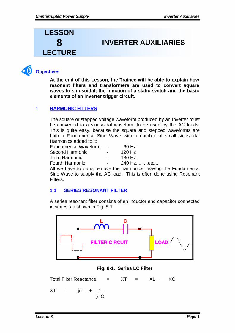
Uninterrupted Power Supply Inverter Auxiliaries
Lesson 8 Page 1
LESSON 8
LECTURE INVERTER AUXILIARIES
Objectives
At the end of this Lesson, the Trainee will be able to explain how resonant filters and transformers are used to convert square waves to sinusoidal; the function of a static switch and the basic elements of an Inverter trigger circuit.
1 HARMONIC FILTERS
The square or stepped voltage waveform produced by an Inverter must be converted to a sinusoidal waveform to be used by the AC loads. This is quite easy, because the square and stepped waveforms are both a Fundamental Sine Wave with a number of small sinusoidal Harmonics added to it: Fundamental Waveform - 60 Hz Second Harmonic - 120 Hz Third Harmonic - 180 Hz Fourth Harmonic - 240 Hz.........etc... All we have to do is remove the harmonics, leaving the Fundamental Sine Wave to supply the AC load. This is often done using Resonant Filters. 1.1 SERIES RESONANT FILTER A series resonant filter consists of an inductor and capacitor connected in series, as shown in Fig. 8-1:
LOAD
L C
FILTER CIRCUIT LOAD
L C
FILTER CIRCUIT
Fig. 8-1. Series LC Filter Total Filter Reactance = XT = XL + XC XT = jωL + _1_ jωC

Uninterrupted Power Supply Inverter Auxiliaries
Lesson 8 Page 2
Maximum power transfer is when XT is zero. At this point, L and C are resonant with each other. Therefore: jωL = _-1_ jωC jωL x jωC = -1 Since (j x j) = -1, ω2 LC = 1 ω2 = _1_ LC So for Resonance: ϖ = _1_ LC Since ω = 2πf, we can match the required values of L and C to the Fundamental Frequency (f0) required. All higher frequencies (i.e. harmonics) will see a high impedance and be eliminated or greatly reduced. Example: A series resonant filter is used to remove harmonics in a square wave of frequency 50 Hz. If the capacitor is 500 µF, calculate: 1. The size of inductor required. 2. The impedance to third harmonics. Answer: 1. ω = 2πf = 2 x π x 50 = 100π ω2 = _1_ L = _1_ LC ω2C L = ______________1______________ 100 x 100 x π x π x 500 x 10-6 L = __ _1____ = 0.02 H = 20 mH. π x π x 5 2. For third harmonics, frequency = 3 x 50 = 150 Hz. ω = 300π and XT = jωL + _1_ jωC XT = j x 300π x 0.02 + ________1__________ j x 300π x 500 x 10-6

Uninterrupted Power Supply Inverter Auxiliaries
Lesson 8 Page 3
XT = (j x 6π) + _-j__ 0.15π XT = j( 6π - __1_ ) 0.15π XT = j(18.852 - 2.114) = j16.74 Ω From the above example, it should be obvious that the Series Resonant Filter acts as a short circuit to the Fundamental Frequency, but is an inductive reactance to any higher frequencies (i.e. harmonics). The higher the harmonic frequency, the greater is the blocking reactance. This is called attenuation, as the ratio of: Output voltage becomes smaller as harmonic frequency rises. Input Voltage The capacitor is only in the circuit to cancel out the inductor at the Fundamental Frequency. For high frequency harmonics, it has very little effect, whereas the inductor has a very high reactance. 1.2 SHUNT RESONANT FILTER This filter consists of an inductor and capacitor connected in parallel, as shown in Fig. 8-2:
LOADL C
FILTER CIRCUIT
LOADL C
FILTER CIRCUIT
Fig. 8-2. Shunt LC Fillter _1_ = _1_ + _1_ XT jωL 1/jωC Maximum power transfer is when XT is infinite. At this point, L and C are resonant with each other. Therefore: jωC = _-1_ jωL jωL x jωC = -1 ω2 LC = 1

Uninterrupted Power Supply Inverter Auxiliaries
Lesson 8 Page 4
ω2 = _1_ LC So for Resonance: ϖ = _1_
LC Note that this is the same equation as for the Series Filter. Since ω = 2πf, we can match the required values of L and C to the Fundamental Frequency (f0) required. All higher frequencies (i.e. harmonics) will see a low shunt impedance and be diverted from the load through the shunt filter. Example: A shunt resonant filter is used to remove harmonics in a square wave of frequency 50 Hz. If the capacitor is 500 µF, calculate: 1. The size of inductor required. 2. The impedance to third harmonics. Answer: 1. We have already done this calculation for the series filter: L = __ _1____ = 0.02 H = 20 mH. π x π x 5 2. For third harmonics, frequency = 3 x 50 = 150 Hz. ω = 2πf = 300π _1_ = _______1______ + j x 300π x 500 x 10-6 XT j x 300π x 0.02 _1_ = -j_ + j x 0.15π = j( -0.053 + 0.471) XT 6π _1_ = j 0.418 XT = 2.24 Ω XT From the above example, it is obvious that the Shunt Resonant Filter acts as an open circuit to the Fundamental Waveform, which bypasses it, but is a low capacitive reactance to harmonics. The higher the harmonic frequency, the lower is this reactance. The inductor is only in the circuit to cancel out the capacitor at Fundamental Frequency. For high frequency harmonics, it has very little effect. For good harmonic filtering, the series and shunt filters are usually combined to produce the Resonant-Arm Filter shown in Fig. 8-3 on the next page.
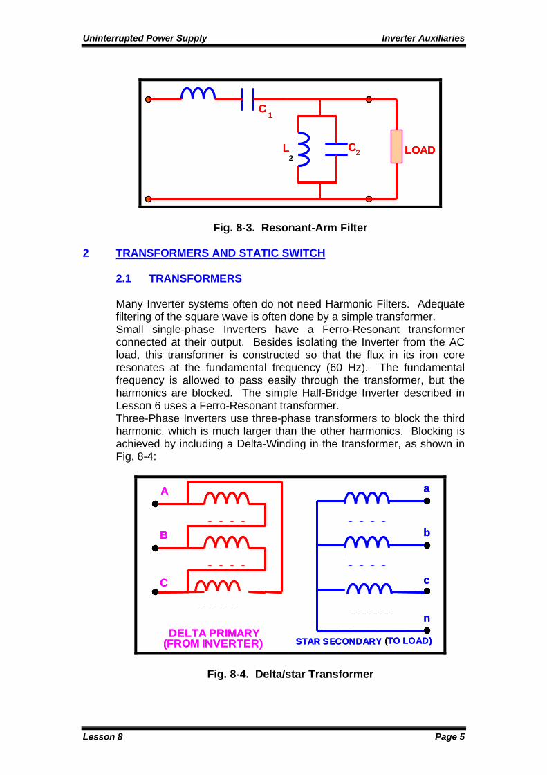
Uninterrupted Power Supply Inverter Auxiliaries
Lesson 8 Page 5
LOADL C2
2
L1 C1
LOADL C2
2
L1 C1
Fig. 8-3. Resonant-Arm Filter
2 TRANSFORMERS AND STATIC SWITCH 2.1 TRANSFORMERS Many Inverter systems often do not need Harmonic Filters. Adequate filtering of the square wave is often done by a simple transformer. Small single-phase Inverters have a Ferro-Resonant transformer connected at their output. Besides isolating the Inverter from the AC load, this transformer is constructed so that the flux in its iron core resonates at the fundamental frequency (60 Hz). The fundamental frequency is allowed to pass easily through the transformer, but the harmonics are blocked. The simple Half-Bridge Inverter described in Lesson 6 uses a Ferro-Resonant transformer. Three-Phase Inverters use three-phase transformers to block the third harmonic, which is much larger than the other harmonics. Blocking is achieved by including a Delta-Winding in the transformer, as shown in Fig. 8-4:
DELTA PRIMARY(FROM INVERTER) STAR SECONDARY (TO LOAD)
A
B
C
a
b
c
nDELTA PRIMARY
(FROM INVERTER) STAR SECONDARY (TO LOAD)
A
B
C
a
b
c
n
Fig. 8-4. Delta/star Transformer

Uninterrupted Power Supply Inverter Auxiliaries
Lesson 8 Page 6
The triplen (3rd, 6th, 9th) harmonics cannot generate a voltage in the star secondary winding because they are in-phase and cancel each other out. The fundamental frequency voltages are 120 degrees out-of-phase, so form a vector triangle and easily generate voltages in the secondary. The result is a fairly smooth sinusoidal output. The voltage vector diagram for a transformer vector group of Dy11 is shown in Fig. 8-5:
A
BC
a
b
c
PRIMARY VOLTAGES SECONDARY VOLTAGES
n
A
BC
a
b
c
PRIMARY VOLTAGES SECONDARY VOLTAGES
n
Fig. 8-5. Voltage Vector Diagram 2.2 STATIC SWITCH Refer back to Fig. 7-6-1 of Lesson 6. The Essential AC Loads Busbars receive power from two inverters and a backup AC supply. The reason is to provide redundancy of inverters - one inverter can be lost (due to maintenance or a fault) without affecting the essential AC loads. However, if one inverter does become faulty (due to insulation or SCR failure) it must be isolated from the Essential AC Loads Busbars as quickly as possible. Otherwise a short circuit in the faulty inverter may be backfed from the busbars, causing major damage and loss of supply. Circuit breakers and relays take a long time to isolate the faulty inverter. To achieve fast isolation times, we use the Static Switch, which is simply two SCRs connected in opposed parallel. A typical configuration is shown in Fig. 8-6:
---
~
+
-
INVERTER
ESSENTIALAC LOADS
L N
x
STATIC SWITCH
T1
T2---
~
+
-
INVERTER
ESSENTIALAC LOADS
L N
x
STATIC SWITCH
T1
T2
Fig. 8-6. Static Switch
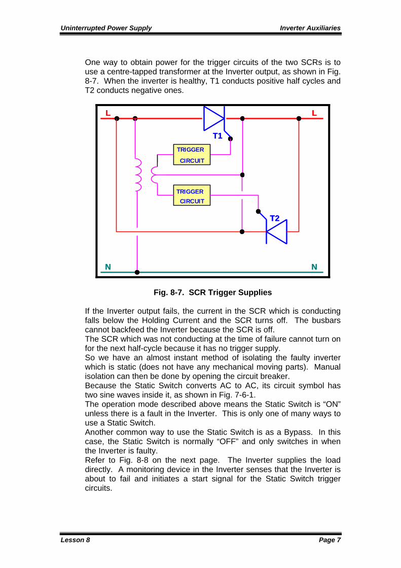
Uninterrupted Power Supply Inverter Auxiliaries
Lesson 8 Page 7
One way to obtain power for the trigger circuits of the two SCRs is to use a centre-tapped transformer at the Inverter output, as shown in Fig. 8-7. When the inverter is healthy, T1 conducts positive half cycles and T2 conducts negative ones.
T1
TRIGGER
TRIGGER
CIRCUIT
CIRCUIT
T2
L L
N N
T1
TRIGGER
TRIGGER
CIRCUIT
CIRCUIT
T2
L L
N N
Fig. 8-7. SCR Trigger Supplies
If the Inverter output fails, the current in the SCR which is conducting falls below the Holding Current and the SCR turns off. The busbars cannot backfeed the Inverter because the SCR is off. The SCR which was not conducting at the time of failure cannot turn on for the next half-cycle because it has no trigger supply. So we have an almost instant method of isolating the faulty inverter which is static (does not have any mechanical moving parts). Manual isolation can then be done by opening the circuit breaker. Because the Static Switch converts AC to AC, its circuit symbol has two sine waves inside it, as shown in Fig. 7-6-1. The operation mode described above means the Static Switch is “ON” unless there is a fault in the Inverter. This is only one of many ways to use a Static Switch. Another common way to use the Static Switch is as a Bypass. In this case, the Static Switch is normally “OFF” and only switches in when the Inverter is faulty. Refer to Fig. 8-8 on the next page. The Inverter supplies the load directly. A monitoring device in the Inverter senses that the Inverter is about to fail and initiates a start signal for the Static Switch trigger circuits.

Uninterrupted Power Supply Inverter Auxiliaries
Lesson 8 Page 8
The standby AC mains supply is therefore brought in parallel with the Inverter output. The total time taken for this is usually about 20 mS. The Inverter’s output contactor then automatically opens, isolating the faulty Inverter from the load in a further 30 mS.
---
~
+
-
INVERTER
L N
x
BYPASS STATIC SWITCH
x
TRIGGER INITIATED BY"INVERTER FAULTY"SIGNAL
CONTACTOR
STANDBY AC SUPPLY
---
~
+
-
INVERTER
L N
x
BYPASS STATIC SWITCH
x
TRIGGER INITIATED BY"INVERTER FAULTY"SIGNAL
CONTACTOR
STANDBY AC SUPPLY
Fig. 8-8. Static Bypass
3 SCR TRIGGERING
The SCRs in rectifiers and inverters need trigger pulses for their gates. So we need Pulse Generators (trigger circuits). With SCR rectifiers, the pulse generator is relatively simple, because it can use the same AC supply as the SCR. Synchronising and timing of the pulses is quite easy, as explained in Lesson 5. With Inverters there is only DC power. So we have to use Oscillators as the pulse generators. An oscillator is supplied with smooth DC voltage and produces alternating waveforms. These waveforms can be square wave, sawtooth wave, sinusoidal or pulses. Capacitors are used in all oscillators to give the Time Delay needed to produce the required waveform. The other main components may be BJT or FET Transistors, Unijunction Transistors (UJTs), Programmable UJTs (PUTs), Crystals or Integrated Circuit Operational Amplifiers. The oscillator design varies enormously from one inverter to another. Popular types are Astable Multivibrators and Crystal Oscillators. The SCR triggering system is also the Voltage Controller. Remember from Lesson 6 that altering the relative firing of the SCRs alters the shape (and so the Average Voltage) of the output from the Inverter. A block diagram of a typical trigger/voltage control system is shown in Fig. 8-9 on the next page. The Pulse Generator takes DC power from the batteries and produces a square-wave output of fixed frequency (60 Hz).

Uninterrupted Power Supply Inverter Auxiliaries
Lesson 8 Page 9
The Trigger Circuit for T1 amplifies the square-wave and supplies the gate of SCR T1 with one positive pulse every 16.67 mS. T1 and T2 provide the positive half-cycles of Inverter output. A similar arrangement exists for T2, except that the trigger pulses can be advanced or retarded compared to those for T1, providing voltage control.
---
~
INVERTER
HARMONICFILTER
STATIC SWITCH
~ ~~
RECTIFIER& DC
FILTER
VOLTAGECOMPARATOR
Does Eout = Eref ?
DC
PHASESHIFTER
(R-C BRIDGE)
CIRCUITFOR T1
TRIGGER
PULSEGENERATOR
INVERTER
(NOT GATE)TO T3/T4
CONTROLS
TO T1 GATE
TO T2 GATETRIGGERCIRCUITFOR T2
---
~
INVERTER
HARMONICFILTER
STATIC SWITCH
~ ~~
RECTIFIER& DC
FILTER
VOLTAGECOMPARATOR
Does Eout = Eref ?
DC
PHASESHIFTER
(R-C BRIDGE)
CIRCUITFOR T1
TRIGGER
PULSEGENERATOR
INVERTER
(NOT GATE)TO T3/T4
CONTROLS
TO T1 GATE
TO T2 GATETRIGGERCIRCUITFOR T2
Fig. 8-9. Trigger/Voltage Control The sinusoidal output voltage from the Inverter and Harmonic Filter is rectified and filtered and fed to a Comparator, where Eout is compared with Eref (the Reference Voltage from a Zener Diode). Any error voltage is then fed to the Phase-Shifter circuit, where it varies the resistance in an R-C Bridge. The square-wave from the Pulse Generator is the input to this R-C Bridge and the output waveform will be phase-shifted (advanced or retarded). This output waveform supplies the Trigger Circuit for T2. The Logic Inverter (Not Gate) phase shifts the output waveform of the Pulse generator by 180 degrees to supply the triggering for SCRs T3 and T4 in the Inverter, which provide the negative half-cycle of the Inverter output. An element not shown is the Synchronising Circuit which is used to ensure the output voltage from the Inverter is synchronised with any existing voltage on the Load Busbars before the Static Switch is closed.

FF II GG UU RR EE SS II NN DD EE XX
Figure No. Page No. Fig. 11 .. 11 ………………………………………………………….. 11
Fig. 11 .. 22 ………………………………………………………….. 22 Fig. 1.3 ………………………………………………………….. 4 Fig. 1.4 …………………………………………………………….5 Fig. 1.5 ……………………………………………………………5 Fig. 1.6 …………………….…………………………………..….6 Fig. 1.7 ……………………………………………………………7 Fig. 2.1 …………………………………………………………… .1 Fig. 2.2 ……………………………………………………….….. 2 Fig. 2.3 …………………………………………………………….3 Fig. 2.4 ……………………………………………………………3 Fig. 2.5 …………………………………………………………….6 Fig. 2.6 ……………………………………………………………6 Fig. 2.7 …………………………………………………….……… .7 Fig. 2.8 …………………………………………………………... 8 Fig. 2.9………………………………..…………………………….8 Fig. 2.10 ……………………………………………………………9 Fig. 2.11 …………………………………………………………...10 Fig. 2.12……………………………………………………………11 Fig. 2.13 ……………………………..…………………………… .11

Fig. 3.1 ………………………………………………………….. 1 Fig. 3.2 …………………………………………………………….2 Fig. 3.3 …………………………………….………………………2 Fig. 3.4 …………………….…………………………………..….3 Fig. 3.5 ……………………………………………………………4 Fig. 3.6 …………………………………………………………… .4 Fig. 3.7 ………………………….…………...……………….….. 5 Fig. 3.8 …………………………..……………..………………….5 Fig. 3.9 ……………………….……………..……………………6 Fig. 3.10……………………………………..…………………….6 Fig. 4.1 …………………….……………..………………………1 Fig. 4.2 ……………………….……………………..…………….2 Fig. 4.3 ……………………….……………………………………2 Fig. 4.4 …………………….…………………………………..….4 Fig. 4.5 ……………………………………………………………5 Fig. 4.6 …………………………………………………………… .5 Fig.4.7 ………………….…………………………………….….. 6 Fig. 5.1 …………………………………………………………….1 Fig. 5.2 …………………….………………………………………3 Fig. 5.3 …………………….…………………………………..….4 Fig. 5.4…………………………………………………..…………4

Fig. 5.5 …………………………………………………………….5 Fig. 5.6 ……………………………………………………….….. 6 Fig. 5.7 …………………………………………………………….7 Fig. 5.8…………………………………………………….………8 Fig5.9………………………………………………………..…….9 Fig.5.10 …………………………………………………………12 Fig. 6.1 ………………………………………………………….1 Fig. 6.2……………………………………………………………2 Fig. 6.3 …………………….…………………………………..….6 Fig. 6.4 ……………………………………………………………6 Fig. 7.1 ………………………………………………..………… .1 Fig.7.2 …………………………………………………….….….. 2 Fig. 7.3 …………………………………………………………… 3 Fig. 7.4 ……………………………………………………….….. 4 Fig. 7.5 ……………………………………………….…………….5 Fig. 7.6………………………………………………..…….………5 Fig7.7…………………………………………………..……..…….6 Fig.7.8 ……………………………………………………..………7 Fig. 7.9 …………………………………………………………….7 Fig. 7.10……………………………………………………………8 Fig. 7.11…………………….…………………………………..…9 Fig. 8.1 …………………………………………………………… .1

Fig. 8.2………………………………………………..……….….. 3 Fig.8.3 ……………………………………………….…………….5 Fig. 8.4…………………………………………….……….………5 Fig8.5……………………………………………….………..…….6 Fig.8.6…………………………………………………...…………6 Fig. 8.7…………………………………………………………….7 Fig. 8.8……………………………………………..………………8 Fig. 8.9…………………….…………………………………..….9