Embed Size (px)
Citation preview

DC-DC Converter with Improved Dynamic Response and
Efficiency Using a Calibrated Auxiliary Phase
by
Yue Wen
A thesis submitted in conformity with the requirementsfor the degree of Master of Applied Science
Graduate Department of Electrical and Computer Engineering
University of Toronto
Copyright© 2011 by Yue Wen
Abstract
DC-DC Converter with Improved Dynamic Response and Efficiency Using a Calibrated
Auxiliary Phase
Yue Wen
Master of Applied Science
Graduate Department of Electrical and Computer Engineering
University of Toronto
2011
A digital adaptive slope control (DASC) technique is presented to improve the dynamic
response and efficiency of a current programmed mode (CPM) buck converter employing
a low-cost auxiliary phase. Compared to the existing nonlinear control techniques, the
advantages of the proposed control scheme include superior voltage droop and settling
time, and on-line calibration to compensate for tolerance in the inductance. The proposed
technique is experimentally verified on a 500 kHz, 10 V to 2.5 V CPM buck converter
prototype. Charge balancing and optimal transient response are achieved for a range of
positive and negative load steps. In addition, compared to a representative single phase
converter, the proposed system not only has better dynamic response but also achieves
2 % heavy-load and 10 % light-load steady-state efficiency improvement. The impact of
the auxiliary phase operation on the converter’s dynamic efficiency is also evaluated at
different load step amplitudes and frequencies.
ii

Acknowledgements
First and foremost, I would like to thank my supervisor, Professor Olivier Trescases,
for his guidance and support during my master study. He was very patient and helpful in
developing my technical and academic skills with his expertise in the power management
field and leadership. His serious academic attitude has greatly influenced me, and will
continue to inspire me for my future studies.
It was my pleasure to work with my friends in the Energy System Group, Amir
Parayandeh and Shahab Poshtkouhi, on different research projects and course work. I
also would like to acknowledge the valuable support of Department of Electrical and
Computer Engineering at University of Toronto, Canadian Microelectronic Corporation,
and Natural Sciences and Engineering Research Council of Canada.
I am also grateful for the moral support and the unconditional love from my parents,
Jixin Zhao and Hualin Wen, and my lovely girlfriend, Pei Yao.
iii

Contents
1 Introduction 1
1.1 Modern DC-DC Converter Applications . . . . . . . . . . . . . . . . . . . 1
1.2 DC-DC Converter Solutions . . . . . . . . . . . . . . . . . . . . . . . . . 4
1.2.1 Computer Power Architecture . . . . . . . . . . . . . . . . . . . . 4
1.2.2 Today’s SMPS Design Challenges . . . . . . . . . . . . . . . . . . 5
1.3 Control Perspective: . . . . . . . . . . . . . . . . . . . . . . . . . . . . . 9
1.3.1 Voltage Mode versus Current Mode . . . . . . . . . . . . . . . . . 9
1.3.2 Analog versus Digital . . . . . . . . . . . . . . . . . . . . . . . . . 12
1.3.3 Linear Control versus Nonlinear Control . . . . . . . . . . . . . . 14
1.4 Thesis Motivation and Objectives . . . . . . . . . . . . . . . . . . . . . . 15
2 Dynamic Response Improvement with Nonlinear Control 20
2.1 Dynamic Response Design Trade-off . . . . . . . . . . . . . . . . . . . . . 20
2.2 Dynamic Response Improvement Techniques . . . . . . . . . . . . . . . . 23
2.2.1 Analog PWM with Internal Current Loop . . . . . . . . . . . . . 23
2.2.2 Time-Optimal Control . . . . . . . . . . . . . . . . . . . . . . . . 25
2.2.3 Steered-Inductor Control . . . . . . . . . . . . . . . . . . . . . . . 26
2.2.4 Current Injection with Switch and Transformer Network . . . . . 27
2.2.5 Auxiliary Phase with Charge Balancing Control . . . . . . . . . . 27
2.3 Digital Adaptive Slope Control (DASC) in Auxiliary Phase . . . . . . . . 31
iv

2.3.1 Ideal Switching Waveform and Timing . . . . . . . . . . . . . . . 32
2.3.2 Transient Response Improvement Analysis . . . . . . . . . . . . . 34
2.4 Light-Load Efficiency Improvement . . . . . . . . . . . . . . . . . . . . . 35
3 Design of CPM Converter with DASC in Auxiliary Phase 43
3.1 Main Phase CPM DC-DC Converter . . . . . . . . . . . . . . . . . . . . 43
3.1.1 Power Stage and Control Circuit . . . . . . . . . . . . . . . . . . 45
3.1.2 Linear Controller Design . . . . . . . . . . . . . . . . . . . . . . . 45
3.2 Design of the Auxiliary Phase . . . . . . . . . . . . . . . . . . . . . . . . 49
3.2.1 Auxiliary Power Stage . . . . . . . . . . . . . . . . . . . . . . . . 49
3.2.2 Counter-based DPWM . . . . . . . . . . . . . . . . . . . . . . . . 49
3.3 Load Step and Transient Detection . . . . . . . . . . . . . . . . . . . . . 50
3.4 DASC Nonlinear Controller . . . . . . . . . . . . . . . . . . . . . . . . . 50
3.5 Self-calibration Against Inductor Tolerance . . . . . . . . . . . . . . . . . 52
3.6 Auxiliary Phase Operation under Light-Load . . . . . . . . . . . . . . . . 54
3.6.1 Main and Auxiliary Phase Shedding . . . . . . . . . . . . . . . . . 54
3.6.2 Auxiliary Phase PFM Controller . . . . . . . . . . . . . . . . . . 55
4 Circuit-Level Simulation and Experimental Results 59
4.1 Circuit-Level Simulation . . . . . . . . . . . . . . . . . . . . . . . . . . . 59
4.1.1 Transient Response . . . . . . . . . . . . . . . . . . . . . . . . . . 59
4.1.2 Load Step Detection . . . . . . . . . . . . . . . . . . . . . . . . . 61
4.1.3 Self-Calibration . . . . . . . . . . . . . . . . . . . . . . . . . . . . 63
4.2 Experimental System and Setup . . . . . . . . . . . . . . . . . . . . . . . 63
4.3 Experimental Results . . . . . . . . . . . . . . . . . . . . . . . . . . . . . 66
4.3.1 Transient Response . . . . . . . . . . . . . . . . . . . . . . . . . . 66
4.3.2 Phase shedding and Mode Switching . . . . . . . . . . . . . . . . 69
4.3.3 Steady-State Efficiency . . . . . . . . . . . . . . . . . . . . . . . . 71
v

4.3.4 Dynamic Efficiency . . . . . . . . . . . . . . . . . . . . . . . . . . 73
5 Conclusions 76
5.1 Thesis Summary and Contributions . . . . . . . . . . . . . . . . . . . . . 76
5.2 Future Work . . . . . . . . . . . . . . . . . . . . . . . . . . . . . . . . . . 78
vi

List of Tables
1.1 LDO and SMPS Comparison . . . . . . . . . . . . . . . . . . . . . . . . . 5
1.2 Intel VRM Design Guidelines 11.1 [5] . . . . . . . . . . . . . . . . . . . . 7
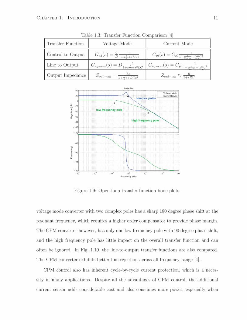
1.3 Transfer Function Comparison [4] . . . . . . . . . . . . . . . . . . . . . . 11
1.4 Traditional Linear Compensator Comparison . . . . . . . . . . . . . . . . 13
2.1 SMPS Design Considerations . . . . . . . . . . . . . . . . . . . . . . . . 21
2.2 Optimal ∆vout and tres Achieved Using Time-Optimal Control . . . . . . 25
2.3 Parameters for the Adaptive Slope Control Scheme . . . . . . . . . . . . 32
2.4 Optimal ∆vout and tres Achieved Using Auxiliary Phase . . . . . . . . . . 34
2.5 Approximate Converter Loss Equations . . . . . . . . . . . . . . . . . . . 35
3.1 Targeted Converter Specification . . . . . . . . . . . . . . . . . . . . . . 44
3.2 Main Phase Power Stage Components . . . . . . . . . . . . . . . . . . . . 45
3.3 Main Phase Control Circuit Components . . . . . . . . . . . . . . . . . . 46
3.4 Auxiliary Phase Power Stage Components . . . . . . . . . . . . . . . . . 49
3.5 Parameters for Phase Switching . . . . . . . . . . . . . . . . . . . . . . . 55
4.1 Experimental Prototype Specifications . . . . . . . . . . . . . . . . . . . 65
4.2 System Parameter and Performance Comparison . . . . . . . . . . . . . . 69
vii

List of Figures
1.1 International Roadmap for Semiconductors report [1] (a) 2000 - 2010 (b)
2010 - 2020. . . . . . . . . . . . . . . . . . . . . . . . . . . . . . . . . . . 2
1.2 Transistor count of (a) modern CPUs and (b) modern GPUs [2]. . . . . . 3
1.3 (a) Computer motherboard power architecture. (b) Computer graphics
card power architecture. . . . . . . . . . . . . . . . . . . . . . . . . . . . 4
1.4 (a) Linear low-dropout regulator and (b) buck switched-mode power sup-
ply [4]. . . . . . . . . . . . . . . . . . . . . . . . . . . . . . . . . . . . . . 6
1.5 A desktop GPU core voltage while running a 3D application. . . . . . . . 8
1.6 (a) Desktop motherboard CPU power supply and (b) Laptop graphics card
GPU power supply. . . . . . . . . . . . . . . . . . . . . . . . . . . . . . . 8
1.7 Buck converter with voltage mode control. . . . . . . . . . . . . . . . . . 9
1.8 Buck converter with CPM control. . . . . . . . . . . . . . . . . . . . . . 10
1.9 Open-loop transfer function bode plots. . . . . . . . . . . . . . . . . . . . 11
1.10 Line-to-output transfer function bode plots. . . . . . . . . . . . . . . . . 12
1.11 Block diagrams of (a) analog controller and (b) digital controller. . . . . 13
1.12 Implementations of (a) analog compensator and (b) digital compensator. 14
1.13 Transient response of (a) linear controller and (b) nonlinear controller with
time-optimal control. . . . . . . . . . . . . . . . . . . . . . . . . . . . . . 15
2.1 Efficiency impact of increasing fs. . . . . . . . . . . . . . . . . . . . . . . 21
viii

2.2 (a) Increase in IL,rms when L is reduced. (b) Impact on efficiency when L
is reduced to achieve better transient response. . . . . . . . . . . . . . . . 22
2.3 Analog compensator with nonlinear control [1]. . . . . . . . . . . . . . . 24
2.4 Waveform of analog linear controller with a nonlinear control loop. . . . . 24
2.5 Ideal switching waveforms for (a) single phase time-optimal control [2–11]
and (b) single phase time-optimal control with current limit [14, 15]. . . . 26
2.6 (a) Buck-derived topology to improve step-down transient [16]. (b) Digi-
tally controlled steered-inductor scheme [17, 18]. . . . . . . . . . . . . . . 27
2.7 Analog current injection using switch and transformer network [19–23]. . 28
2.8 Decoupled transient response and efficiency trade-off using a small auxil-
iary phase [24–29]. . . . . . . . . . . . . . . . . . . . . . . . . . . . . . . 28
2.9 Ideal waveforms for (a) single turn on-and-off operation in auxiliary phase
[26, 27] and (b) auxiliary phase operated as constant current source [28, 29]. 29
2.10 Simplified architecture of the CPM buck converter with auxiliary phase. . 31
2.11 Ideal waveforms of the proposed solution for (a) positive load step and (b)
negative load step. . . . . . . . . . . . . . . . . . . . . . . . . . . . . . . 33
2.12 Comparison between the constant current source approach [28,29] and the
proposed approach. . . . . . . . . . . . . . . . . . . . . . . . . . . . . . . 34
2.13 Calculated percentage of different losses. . . . . . . . . . . . . . . . . . . 36
2.14 Calculated overall efficiency achieved by changing to different phases and
modes of operation. . . . . . . . . . . . . . . . . . . . . . . . . . . . . . . 36
3.1 Simplified architecture of the CPM buck converter with auxiliary phase. . 44
3.2 Structure of the dead-time generator. . . . . . . . . . . . . . . . . . . . . 46
3.3 Structure of the linear PI controller. . . . . . . . . . . . . . . . . . . . . . 47
3.4 Bode plots of the converter and compensator transfer functions. . . . . . 48
3.5 Bode plots of the compensated system. . . . . . . . . . . . . . . . . . . . 48
3.6 Structure of the auxiliary phase DPWM. . . . . . . . . . . . . . . . . . . 50
ix

3.7 Architecture of the digital controller. . . . . . . . . . . . . . . . . . . . . 51
3.8 Ideal waveforms of the calibration scheme. . . . . . . . . . . . . . . . . . 53
3.9 Phase switching between main and auxiliary phase. . . . . . . . . . . . . 54
3.10 Architecture of the digital PFM controller. . . . . . . . . . . . . . . . . . 55
4.1 Cadence AMS simulation of the three discussed techniques for a 3.2 A
negative load step. . . . . . . . . . . . . . . . . . . . . . . . . . . . . . . 60
4.2 Cadence AMS simulation of the proposed scheme response at four different
load current slew rates for a 5 A negative load step. . . . . . . . . . . . . 61
4.3 AMS simulation showing the movement of the valley point for different
values of Resr. . . . . . . . . . . . . . . . . . . . . . . . . . . . . . . . . . 62
4.4 AMS simulation of the proposed calibration scheme . . . . . . . . . . . . 63
4.5 AMS simulation of the response after calibration. . . . . . . . . . . . . . 64
4.6 Dc-dc converter prototype. . . . . . . . . . . . . . . . . . . . . . . . . . . 64
4.7 Experimental setup. . . . . . . . . . . . . . . . . . . . . . . . . . . . . . 65
4.8 Block diagram of the experimental setup. . . . . . . . . . . . . . . . . . . 66
4.9 Dynamic response for (a) positive ∆iout of 2.1 A (4 µs/div, 2.5 A/div) and
(b) negative ∆iout of 2.1 A (4 µs/div, 2.5 A/div). . . . . . . . . . . . . . 67
4.10 Main phase operation for (a) positive ∆iout of 3.2 A (2 µs/div, 2 A/div)
and (b) negative ∆iout of 3.2 A (3 µs/div, 2 A/div). . . . . . . . . . . . . 67
4.11 Auxiliary phase and load detection circuit operations for (a) positive ∆iout
of 3.2 A (2 µs/div, 2.5 A/div) and (b) negative ∆iout of 3.2 A (3 µs/div,
2.5 A/div). . . . . . . . . . . . . . . . . . . . . . . . . . . . . . . . . . . 68
4.12 Dynamic response of a negative ∆iout of 3.2 A for (a) proposed system (4
µs/div, 2.5 A/div) and (b) single-phase system with time-optimal control
(4 µs/div, 2 A/div). . . . . . . . . . . . . . . . . . . . . . . . . . . . . . . 68
4.13 Switching from the main phase to the auxiliary phase. . . . . . . . . . . . 69
4.14 Switching from PWM to PFM mode in the auxiliary phase. . . . . . . . 70
x

4.15 Steady-state operation of PFM mode in the auxiliary phase. . . . . . . . 70
4.16 Measured switching frequency versus load current in PFM mode. . . . . . 71
4.17 Steady-state efficiency comparison in PWM mode. . . . . . . . . . . . . . 72
4.18 Steady-state efficiency in logarithm. . . . . . . . . . . . . . . . . . . . . . 72
4.19 Full range steady-state efficiency comparison. . . . . . . . . . . . . . . . 73
4.20 Waveforms during a 10 kHz, 50% duty ratio and 1 A to 5.2 A load tran-
sients for (a) proposed system (50 µs/div, 2.5 A/div) and (b) single-phase
system with time-optimal control (50 µs/div, 2.5 A/div). . . . . . . . . . 74
4.21 Dynamic efficiency Comparison for 1 - 3.1 A and 1 - 5.2 A load transients. 74
xi

Chapter 1
Introduction
This chapter gives a brief introduction of modern dc-dc converter solutions. The con-
verter applications and design challenges are presented in Section 1.1 and Section 1.2,
respectively. Section 1.3 discusses the converter operation from the control perspectives.
The thesis motivation and objectives are presented in Section 1.4.
1.1 Modern DC-DC Converter Applications
In today’s semiconductor industry, extensive research is being conducted to make comput-
ing hardware faster and cheaper by developing more complex computing architectures
using small feature size transistors. The supply voltage is also scaled down to reduce
the power consumption. From 2000 to 2010, the International Technology Roadmap
for Semiconductor has reported a printed gate length reduction from 130 nm to 40 nm
and a supply voltage reduction from 1.5 V to below 1 V for microprocessors, as shown
in Fig. 1.1(a) [1]. The device current and power consumption, however, have nearly
tripled [1] due to the increase in system complexity and transistor count. The recent de-
velopment in CMOS technologies will continue to follow the famous Moore’s law, which
predicted the transistor count on the same die area would double every two years, as in-
dicated in Fig. 1.1(b). As the supply voltage continues to scale down, the device current
1

Chapter 1. Introduction 2
can reach as high as 200 A. Interestingly, the total device power is predicted to stay under
150 W until 2020. This is a result of the existing challenges of power delivery and heat
dissipation, which require expensive power supply components and cooling solutions [1].
130 nm
90 nm 75 nm
65 nm 54 nm
54 nm 54 nm 54 nm 47 nm
47 nm41 nm
0.6
0.8
1
1.2
1.4
1.6
100
150
200
250
300
Su
pp
ly V
olt
ag
e (
V)
Cu
rre
nt
(A),
Po
we
r (W
)
Current
Power
Suppy Voltage
0
0.2
0.4
0
50
2000 2001 2002 2003 2004 2005 2006 2007 2008 2009 2010
C
Year, Gate Length (nm)
(a)
47 nm41 nm
35 nm28 nm
25 nm22 nm
20 nm 18 nm16 nm 14 nm
12.5 nm
0.4
0.6
0.8
1
1.2
100
150
200
250
300
Su
pp
ly V
olt
ag
e (
V)
Cu
rren
t (A
), P
ow
er
(W)
Current
Power
Suppy Voltage
0
0.2
0
50
2010 2011 2012 2013 2014 2015 2016 2017 2018 2019 2020
C
Year, Gate Length (nm)
(b)
Figure 1.1: International Roadmap for Semiconductors report [1] (a) 2000 - 2010 (b)
2010 - 2020.
Among all the digital CMOS integrated circuits for computing, the central processing
unit (CPU) and graphics processing unit (GPU) are the most power-hungry devices. The

Chapter 1. Introduction 3
Pentium 4 Atom
Itanium 2Core 2 Duo
Core i7
Six-Core Core i7
Dual-Core Itanium
Six-Core Xeon
Quad-Core Itanium Tukwila
8-Core Xeon Nehalem
K7
Barton
K8
K10 65nm
K10 45nm
Six-Core Opteron
Cell
POWER6
POWER7
100
1000
10000
nsi
stor
Co
un
t (M
illi
on)
Pentium
Pentium II
Pentium III
K5
K6
1
10
1992 1994 1996 1998 2000 2002 2004 2006 2008 2010 2012
Tra
n
Year
Intel
AMD
IBM
(a)
R100
R200
RV200
R300
RV250
R360
RV350
RV280
R480
R370
RV410
R520
RV530
RV515
R580RV570
R600
RV630
RV610
RV670
RV770
RV730
RV635
RV620RV710
RV740
Cypress
Juniper
Redwood
Ceder
NV10NV15
NV20
NV18
NV25
NV30NV35
NV36
NV40
NV43
NV44
G70
NV42
G80
G71
G73 G86
G84
G92
G94
GT200
GF100
100
1000
10000
nsi
sto
r C
ou
nt
(Mil
lio
n)
1
10
1999 2001 2003 2005 2007 2009 2011
Tra
n
Year
AMD/ATI
NVIDIA
(b)
Figure 1.2: Transistor count of (a) modern CPUs and (b) modern GPUs [2].
transistor counts of various CPUs and GPUs from major semiconductor manufactures
are listed in Fig. 1.2. The transistor count for both of the devices has increased by about
100× over the past decade [2]. High-end CPU and GPU systems also have a parallel
multi-core architecture to achieve higher performance. These devices create a demand
for power supplies with extremely high power densities and fast dynamic response [3]. In

Chapter 1. Introduction 4
turn, the performance of the power supply under high dynamic load can greatly impact
the processor’s performance benchmarks.
1.2 DC-DC Converter Solutions
1.2.1 Computer Power Architecture
Computer
Motherboard
12V, 5V, 3.3V BUS
(a)
12V, 3.3V BUS
12V BUS
Computer
Graphics Board
(b)
Figure 1.3: (a) Computer motherboard power architecture. (b) Computer graphics card
power architecture.
In order to fulfill the increasing power requirement of computer systems, the power
architecture shown in Fig. 1.3, was established for typical desktop systems. An ac-
dc power supply unit (PSU) is used to produce multiple dc output voltages to power
peripherals and on-board dc-dc power supplies. The on-board dc-dc converters step

Chapter 1. Introduction 5
down the dc voltages to power digital VLSI loads such as CPUs, GPUs and other ICs
with high efficiency and tight regulation. They are often referred as Point-of-Load (PoL)
converters.
Table 1.1: LDO and SMPS Comparison
Comparison LDO SMPS
Best-Case Power Efficiency Vout/Vin 100 %
Control Bandwidth high (MHz) bounded by fs (kHz)
Line Rejection high medium
Applications low-power (several watts) high-power (up to 100s watts)
Inductive Components No Yes
Two types of regulators, linear low-dropout regulator (LDO) and switched-mode
power supply (SMPS), are typically used for PoL applications, as shown in Fig. 1.4(a)
and (b), respectively. LDO is usually used for low current and medium conversion ratio
applications since it does not require inductive components, which makes it easier to im-
plement on-chip. The disadvantage is that LDOs only offer a best-case power conversion
efficiency of Vout/Vin. LDOs are therefore often used for powering display connectors
and low-power ICs. For power-hungry devices such as the CPU, GPU and memory, the
non-isolated buck SMPS is widely used. SMPS offers an ideal power conversion efficiency
of 100 %, but suffers from switching noise and more complex control design compared to
LDO [4]. A general comparison between LDO and SMPS is provided in Table 1.1.
1.2.2 Today’s SMPS Design Challenges
As discussed in Section 1.1, modern CPUs and GPUs consume more than 100 A at sub-
1 V, and their power supplies have strict requirements on the efficiency and dynamic
response. SMPS is therefore commonly used due to its ideal efficiency of 100 %, and it
can be interleaved to produce higher power. A SMPS module for microprocessors is also

Chapter 1. Introduction 6
+
-
Load
VREF
inVoutV
inCoutC1R
2R
pM
(a)
L
outCLoad
inC
H(s)
+-Gc(s)PWM
inVoutV
VREFCompensator
Controller
hM
lM1c
2c
errVcV
(b)
Figure 1.4: (a) Linear low-dropout regulator and (b) buck switched-mode power supply
[4].
commonly referred as a voltage regulator module (VRM). The Voltage Regulator Module
(VRM) and Enterprise Voltage Regulator-Down (EVRD) design guidelines published
regularly by Intel specifies the design requirements for power supply designers. Some of
the specifications in the latest 11.1 edition are listed in Table 1.2.
The specification that draws the most attention, is the large load step of 120 A that
occurs at a rate of up to 50 kHz, and the current slew rate is as high as 300 A/µs.
Despite the high load dynamics, the output voltage is required to have a maximum
undershoot and overshoot of only 50 mV. This requirement is essential to the operation
of the microprocessor, because it determines the nominal operating voltage, Vnominal, of

Chapter 1. Introduction 7
Table 1.2: Intel VRM Design Guidelines 11.1 [5]
Specifications Contents
Maximum Continuous Load Current 130 A
Maximum Peak Load Current 150 A
Maximum Load Current Step 120 A
Full Load Step Rep Rate 50 kHz
Maximum Current Slew Rate 300 A/µs
Output Voltage Ripple 10 mVp−p
Maximum Overshoot, Duration 50 mV, 25 µs
the processor which should be at least the amount of maximum undershoot, vu,max, higher
than the minimum allowable voltage, Vmin, as shown in (1.1). A technique referred as
adaptive voltage positioning (AVP) was developed to adaptively adjust the voltage level
to anticipate the load steps [6]. Using AVP, the allowable voltage window, (Vmax - Vmin),
can be reduced. Frequent high overshoot also results a higher average operating voltage,
which effectively reduces the processor’s lifetime.
Vnominal ≥ Vmin + ∆vu,max. (1.1)
With a VRM design having fast transient response, the processor can be operated at
a lower voltage, which reduces the power consumption. It is however, very difficult to
achieve the optimal transient response and efficiency due to the constrains in the physical
space and the cost of both components and cooling. A capture of a desktop GPU core
voltage while running a 3D application is shown in Fig. 1.5. The core voltage continuously
fluctuates due to the fast change in the load current. Pictures of a typical desktop
motherboard and laptop graphics card are shown in Fig. 1.6(a) and (b), respectively. The
VRM layout space is very limited, and laptop design also requires low profile components.
High efficiency VRMs require power components with low resistance, and the transient
response can be improved by having a large volume of output capacitance. The cost and

Chapter 1. Introduction 8
Figure 1.5: A desktop GPU core voltage while running a 3D application.
(a) (b)
Figure 1.6: (a) Desktop motherboard CPU power supply and (b) Laptop graphics card
GPU power supply.
space constraints however, usually limit the use of expensive power components and large
volume of capacitance, therefore it is essential to develop circuit and control techniques to
improve efficiency and dynamic response without using expensive components [3, 7–12].

Chapter 1. Introduction 9
1.3 Control Perspective:
Voltage mode and current mode control are commonly used in the control of power
electronics. In both cases, a feedback system is formed with a compensator to stabilize
the control loop. In order to check the converter’s stability, the converter is first converted
to a linear model. By applying a small disturbance, the control to output transfer function
can be obtained. The compensation is then designed to provide the required bandwidth
and phase margin. The compensator can be implemented in either analog or digital form.
Although analog control is widely used in commercial power management solutions, there
has been increasing interest in digital control. Furthermore, nonlinear control techniques
have been developed to offer improvements in converter performance. The details of
different control perspectives are discussed in the following subsections.
1.3.1 Voltage Mode versus Current Mode
L
outCLoad
inC
H(s)
+-PIDPWM
inVoutV
VREFCompensator
Voltage mode
Controller
hM
lM1c
2c
errVcV
Figure 1.7: Buck converter with voltage mode control.

Chapter 1. Introduction 10
L
outCLoad
inC
H(s)
PI
Deadtime
inVoutV
VREFCompensator
Current mode
Controller
hM
lM1c
2c
errVcV
+
-
S
R
Q
clock
+-
++
Rf
Slope comp
Figure 1.8: Buck converter with CPM control.
Buck converters using voltage mode and current mode control are shown in Fig. 1.7
and 1.8, respectively. This work focuses on peak current mode control. There are also
other current mode control schemes such as average current mode control [13] and valley
current mode control [14] which are not discussed here. A current programmed mode
(CPM) buck converter includes an internal current loop which consists of an additional
current sensor and slope compensation. The converter transfer functions can be derived
using small signal analysis, and they are listed in Table 1.3. One major advantage of
the additional internal current loop of the CPM converter is that its control-to-output
transfer function has two real poles, a dominant low frequency pole and a high frequency
pole that is often neglected, whereas two complex poles are present in voltage mode
control. A simpler compensator can therefore be used to stabilize a converter with CPM
control [4].
The bode plots of the control-to-output transfer functions are shown in Fig. 1.9. The
Chapter 1. Introduction 11
Table 1.3: Transfer Function Comparison [4]
Transfer Function Voltage Mode Current Mode
Control to Output Gvd(s) = VD
11+s L
R+s2LC
Gvi(s) = Gc01
1+ sQcωc
+( sωc
)2
Line to Output Gvg−vm(s) = D 11+s L
R+s2LC
Gvg−cm(s) = Gg01
1+ sQcωc
+( sωc
)2
Output Impedance Zout−vm = Ls
1+ LR
s+LCs2Zout−cm ≈
R1+sRC
-120
-100
-80
-60
-40
-20
0
20
40
Ma
gn
itu
de
(d
B)
101
102
103
104
105
106
107
-180
-135
-90
-45
0
Ph
ase
(d
eg
)
Bode Plot
Frequency (Hz)
Voltage Mode
Current Mode
low frequency pole
high frequency pole
complex poles
Figure 1.9: Open-loop transfer function bode plots.
voltage mode converter with two complex poles has a sharp 180 degree phase shift at the
resonant frequency, which requires a higher order compensator to provide phase margin.
The CPM converter however, has only one low frequency pole with 90 degree phase shift,
and the high frequency pole has little impact on the overall transfer function and can
often be ignored. In Fig. 1.10, the line-to-output transfer functions are also compared.
The CPM converter exhibits better line rejection across all frequency range [4].
CPM control also has inherent cycle-by-cycle current protection, which is a neces-
sity in many applications. Despite all the advantages of CPM control, the additional
current sensor adds considerable cost and also consumes more power, especially when

Chapter 1. Introduction 12
101
102
103
104
105
106
-100
-80
-60
-40
-20
0
20
Ma
gn
itu
de
(d
B)
Bode Plot
Frequency (Hz)
Voltage Mode
Current Mode
Improved line rejection in
current mode converter
Figure 1.10: Line-to-output transfer function bode plots.
the switching frequency, fs, increases to several MHz. These disadvantages are more
pronounced in high frequency integrated converter designs. There is extensive research
that focuses on low-power current sensor and sensor-less CPM designs to address these
disadvantages [15, 16].
1.3.2 Analog versus Digital
A typical analog controller is shown in Fig. 1.11(a), and is widely used in today’s power
supply controller design. The pulse-width-modulator (PWM) signal is generated by
comparing the compensated control signal vc to a sawtooth signal which has a frequency
of fs. In Fig. 1.11(b), the block diagram of a digital controller is illustrated. An ADC is
needed to convert the output voltage to the digital domain. The error signal e[n] is then
passed to the digital compensator to obtain the duty cycle D[n]. A digital pulse-width-
modulation (DPWM) is used to produce the gating signals c1 and c2 [17, 18].
The expressions of the commonly used continuous-time proportional-integral (PI)
and proportional-integral-derivative (PID) compensators are shown in Table 1.4. Digital
PI and PID compensators can be derived directly from their analog forms based on s-
domain to z-domain transformation. The practical implementations of the analog and

Chapter 1. Introduction 13
H(s)+
-Dead
Timeoutv
VREF
Analog
Compensator
Analog
Controller
1c 2c
)(tverr)(tvc Gc(s)+
-
Sawtooth
(a)
H(s)Dead
Time outv
VREF
Digital
Compensator
Digital
Controller
1c 2c
][ne][nDGc(z)DPWM ADC
(b)
Figure 1.11: Block diagrams of (a) analog controller and (b) digital controller.
digital compensators are shown in Fig. 1.12(a) and (b), respectively. In the analog
compensator, discrete resistors and capacitors are used to allow designers to adjust the
compensation. In the digital compensator, the coefficients can be either hard-coded or
programmable. This is one of the advantages of digital control, which allows on-line
compensator optimization without additional external passive components [17, 18].
Table 1.4: Traditional Linear Compensator Comparison
Analog Digital
PI Gcm(1 + ωL
s) D[n] = D[n − 1] + c1 · e[n] + c2 · e[n − 1]
PID Gcm(1 + ωL
s)(1 + s
ωz) D[n] = D[n − 1] + c1 · e[n] + c2 · e[n − 1] + c3 · e[n − 2]

Chapter 1. Introduction 14
+
-
VREF1R
2R
3R
4R
1C2C
3C
)(tvout)(tvc
(a)
Z-1
][ne
Z-1
Z-1
x
x
x
]1[ ne
]2[ ne
1c
2c
3c
+][nd
]1[ nd
D QZ
-1
clk
(b)
Figure 1.12: Implementations of (a) analog compensator and (b) digital compensator.
1.3.3 Linear Control versus Nonlinear Control
Linear control has proven to be highly reliable in the control of SMPS. A typical response
of a buck converter for a positive current step is shown in Fig. 1.13(a). With a properly
designed compensator, the inductor current, iL(t), settles to the new load current without
oscillations, and the output voltage, vout(t), recovers to the nominal voltage smoothly.
iL(t) is however, slowly increased due to the limited bandwidth, which results a large
undershoot. Using nonlinear control, the controller can force iL(t) to increase until the
load current is reached, and this results the optimal transient response independent of
fs [19], as illustrated in Fig. 1.13(b). This technique is commonly referred as time-optimal
control, and it has been demonstrated with both analog and digital implementations.

Chapter 1. Introduction 15
iL(t)
iout (t) outi =Q1 Q2
Q1
Q2
vout (t)
outv esrv
rest
(a)
iL(t)
iout (t) outi =Q1 Q2
Q1
Q2
vout (t)
outv esrv
rest
(b)
Figure 1.13: Transient response of (a) linear controller and (b) nonlinear controller with
time-optimal control.
Various other nonlinear control techniques are also developed to meet the ever-growing
demand of fast response power supplies.
1.4 Thesis Motivation and Objectives
The goal of this work is to develop a digital nonlinear control technique that allows
the converter to have optimal dynamic response and improved efficiency. The control
scheme should address the problems in the existing nonlinear control schemes, which are

Chapter 1. Introduction 16
robustness and incremental cost.
More specifically, a single-phase CPM buck converter is designed with a small aux-
iliary phase to optimize the transient response. The target application is a single phase
PoL application with strict dynamic response and efficiency requirements. The digital
controller must have all the following functions: Precise charge balancing control that is robust against different load step sizes and
slew rates. Accurate transient and load step detection. Calibration against the inductor tolerance to ensure the accuracy of the charge
balancing operation. Phase shedding and PWM/PFM dual mode operation to improve light-load effi-
ciency with auxiliary phase.
The efficiency impact of the auxiliary phase operation and its benefit of light-load
efficiency improvement must also be investigated, which will further justify the benefits
of the proposed converter system.
The thesis is organized as follows, Chapter 2 discusses the existing nonlinear control
techniques, and introduces the proposed control scheme. Chapter 3 shows the detailed
implementation of the SMPS and nonlinear digital controller. The system and circuit
level simulation and experimental results are presented in Chapter 4. The conclusions
and future work are discussed in Chapter 5.

References
[1] “International technology roadmap for semiconductors, 2010 update.”
http://www.itrs.net/reports.html.
[2] “Transistor count of CPUs, GPUs and FPGAs, 2011 update.”
http://en.wikipedia.org/wiki/Transistorcount.
[3] M. Zhang, M. Jovanovic, and F. Lee, “Design considerations for low-voltage on-
board DC/DC modules for next generations of data processing circuits,” IEEE
Transactions on Power Electronic, vol. 11, pp. 328–337, Mar. 1996.
[4] R. Erickson and M. D., Fundamentals of Power Electronics, 2nd ed. Springer, 2001.
[5] “Voltage regulator module (VRM) and enterprise voltage
regulator-down (EVRD) 11.1 design guidelines, Sep. 2009.”
http://www.intel.com/assets/PDF/designguide/321736.pdf.
[6] M. Zhang, “Powering intel pentium 4 generation processors,” in Electrical Perfor-
mance of Electronic Packaging, 2001, pp. 215–218, 2001.
[7] A. Rozman and K. Fellhoelter, “Circuit considerations for fast, sensitive, low-voltage
loads in a distributed power system,” in Applied Power Electronics Conference and
Exposition, 1995, vol. 1, pp. 34–42, Mar. 1995.
[8] J. O’Connor, “Converter optimization for powering low voltage, high performance
17

REFERENCES 18
microprocessors,” in Applied Power Electronics Conference and Exposition, 1996,
vol. 2, pp. 984–989, Mar. 1996.
[9] R. Redl, B. Erisman, and Z. Zansky, “Optimizing the load transient response of
the buck converter,” in Applied Power Electronics Conference and Exposition, 1998,
vol. 1, pp. 170–176, Feb. 1998.
[10] Y. Panov and M. Jovanovic, “Design considerations for 12-V/1.5-V, 50-A voltage
regulator modules,” IEEE Transactions on Power Electronics, vol. 16, pp. 776–783,
Nov. 2001.
[11] J. Wei, P. Xu, H.-P. Wu, F. Lee, K. Yao, and M. Ye, “Comparison of three topology
candidates for 12-V VRM,” in Applied Power Electronics Conference and Exposition,
2001, vol. 1, pp. 245–251, 2001.
[12] J. Sun, “Control design considerations for voltage regulator modules,” in Telecom-
munications Energy Conference, 2003, pp. 84–91, Oct. 2003.
[13] P. Ninkovic and M. Jankovic, “Improved average inductor current control of the
constant frequency dc/dc converters using the tuned-average current-mode,” in Pro-
ceedings of the 24th Annual Conference of the IEEE Industrial Electronics Society,
1998, vol. 2, pp. 646–650, Aug. 1998.
[14] “ADP1874, Synchronous Buck Controller with Constant On-Time and Valley Cur-
rent Mode.” Analog Devices, Inc.
[15] O. Trescases, A. Parayandeh, A. Prodic, and W. T. Ng, “Sensorless digital peak
current controller for low-power dc-dc smps based on a bi-directional delay line,” in
IEEE Power Electronics Specialists Conference, 2007, pp. 1670–1676, Jun. 2007.
[16] Z. Lukic, S. Ahsanuzzaman, A. Prodic, and Z. Zhao, “Self-tuning sensorless digital
current-mode controller with accurate current sharing for multi-phase dc-dc convert-

REFERENCES 19
ers,” in Applied Power Electronics Conference and Exposition, 2009, pp. 264–268,
Feb. 2009.
[17] O. Trescases, “Design of advanced high-frequency switched mode power supplies.”
ECE1084H Lecture, 2010.
[18] A. Prodic, “Design of high-frequency switch-mode power supplies.” ECE1066H Lec-
ture, 2009.
[19] Z. Zhao and A. Prodic, “Continuous-time digital controller for high-frequency dc-dc
converters,” IEEE Transactions on Power Electronics, vol. 23, pp. 564–573, Mar.
2008.

Chapter 2
Dynamic Response Improvement
with Nonlinear Control
Both analog and digital nonlinear controllers have been developed to push the dynamic
response of dc-dc converters to the physical limit imposed by the LC filter. They are
discussed in detail in this Chapter. The dynamic response and efficiency trade-off is
discussed in Section 2.1. The existing nonlinear control schemes are presented in Section
2.2. Section 2.3 introduces the proposed DASC scheme in the auxiliary phase. The
light-load efficiency improvement that can be achieved by using the auxiliary phase is
discussed in Section 2.4.
2.1 Dynamic Response Design Trade-off
Power supply designers usually have to constantly make trade-offs among many design
considerations. The main design considerations are listed in Table 2.1. The most obvious
trade-offs are usually related to cost. For example, choosing low Ron power transistors and
low ESR capacitors can yield better efficiency and output ripple, but these components
tend to be more expensive. It is therefore beneficial to develop system level techniques
that decouple some of these trade-offs. This makes it easier for designers to meet the
20

Chapter 2. Dynamic Response Improvement with Nonlinear Control 21
specifications.
Table 2.1: SMPS Design Considerations
Efficiency
Steady-State Output Ripple
Dynamic Response
Line Rejection
EMI
Thermal Performance
Short Circuit Protection
Peak Current Protection
Cost
Layout Area
Life Time
30%
40%
50%
60%
70%
80%
90%
100%
Eff
icie
ncy
fs = 500 kHzVi = 10 V
Decrease in efficiency due to
increase in switching frequency fs.
0%
10%
20%
30%
0 1 2 3 4 5 6 7 8
Load Current (A)
fs = 1 MHz
fs = 2 MHz
Vin 10 V
Vout = 2.5 V
fs = 500 kHz
Figure 2.1: Efficiency impact of increasing fs.
Due to the fast change in load current and the low supply voltage of modern ap-
plications, meeting the dynamic response requirement has become a major challenge,

Chapter 2. Dynamic Response Improvement with Nonlinear Control 22
2
3
4
5
6
i L,r
ms
(A
)
L = 10 uH
Increase in rms current due to
lower inductance used.
Vin = 10 V
Vout = 2.5 V
fs = 500 kHz
0
1
2
0.5 5
Load Current (A)
L = 3.3 uH
L = 1.5 uH
L = 1 uH
(a)
85%
90%
95%
Eff
icie
ncy
L = 10 uH
Vin = 10 V
Vout = 2.5 V
fs = 500 kHz
Decrease in efficiency due to
lower inductance used.
75%
80%
0.5 5
Load Current (A)
L = 3.3 uH
L = 1.5 uH
L = 1 uH
(b)
Figure 2.2: (a) Increase in IL,rms when L is reduced. (b) Impact on efficiency when L is
reduced to achieve better transient response.
especially with additional cost and area constraints. Using the traditional analog lin-
ear control, dynamic response is limited by the controller bandwidth and the inductor
current slew rate for a given output capacitance. The bandwidth of the control loop is
ultimately limited by fs. Increasing in fs to improve the dynamic response results in

Chapter 2. Dynamic Response Improvement with Nonlinear Control 23
higher switching loss and gate-drive loss, therefore has a negative impact on the con-
verter efficiency, as illustrated in Fig. 2.1. High switching and gate-drive losses are the
major concerns that prevent the increase of fs, although operating at higher fs reduces
the size of L and Cout. Furthermore, using a lower inductance which yields higher in-
ductor current slew rate, diL/dt, can also improve the transient response. This is done
by increasing output capacitance and reducing inductance so that the resonant 12π
√LC
is
unchanged, therefore no change in compensation is needed. The main drawback is that
reducing L increases inductor current ripple, ∆iL, given by (2.1), which results a higher
RMS current, as shown in Fig. 2.2(a). All the resistive losses are therefore increased. The
resulting impact on the efficiency is illustrated in Fig. 2.2 (b). The output voltage ripple,
∆vout, also increases with ∆iL given by (2.2). It is therefore very beneficial to develop
techniques that can decouple the transient response and efficiency trade-off so that the
dynamic response requirement can be met without negatively impacting efficiency and
output voltage ripple.
∆iL =Vg − Vout
LDTs (2.1)
∆vout ≈∆iLTs
8Cout
+ ∆iLResr (2.2)
2.2 Dynamic Response Improvement Techniques
This section reviews existing nonlinear control techniques for dynamic response improve-
ment. The advantages and disadvantages of each scheme are presented.
2.2.1 Analog PWM with Internal Current Loop
Most analog PWM controllers are based on linear compensator designs that have a control
bandwidth limited by fs. The information of the load current is essential for any nonlinear
controllers. For example, the LM3753 controller IC, as shown in Fig. 2.3, combines the

Chapter 2. Dynamic Response Improvement with Nonlinear Control 24
outputs from the inductor DCR current sensing circuit and the filtered version as the
average current to achieve faster transient response [1]. The transient waveforms are
shown in Fig. 2.4. The high-side MOSFET is fully turned on until load current has been
reached. This can guarantee the minimum voltage droop, and the response time is also
improved from the traditional linear control.
H(s)
Dead
Time
outv
VREF
Analog Controller With
Internal Current Loop
1c 2c
FB
)(tvc
External
Compensator
Gc(s)+
-
Sawtooth
+
-
COMP
External RC
DCR Sensing+
-
+
IAVE
CS
Internal Current Loop
Figure 2.3: Analog compensator with nonlinear control [1].
iL(t)
iout (t) outi =Q1 Q2
Q1
Q2
vout (t)
outv esrv
rest
Figure 2.4: Waveform of analog linear controller with a nonlinear control loop.

Chapter 2. Dynamic Response Improvement with Nonlinear Control 25
2.2.2 Time-Optimal Control
Another technique is commonly referred as time-optimal control, which has been proven
to achieve the optimal response limited by the LC filter, without any modification to
the power stage. Analog implementations have been presented which utilize analog in-
tegrators to achieve capacitor charge balance [2] or a second-order switching surface
in boundary control [3–5]. Digital implementations of time-optimal control have also
been demonstrated on single phase voltage mode converters [6–11], multiphase voltage
mode [12] and current mode [13] converters. The time-optimal switching waveforms for
a single phase buck converter are shown in Fig. 2.5(a), and the ideal voltage droop ∆vout
and settling time tres are given in Table 2.2. In [14, 15], the concept of current limited
time-optimal control is introduced, as shown in Fig. 2.5(b). In this approach, the peak
inductor current is limited at the expense of a longer settling time such that an inductor
with lower saturation current can be used. The use of nonlinear time-optimal control
decouples the dependence of dynamic response on the converter’s control bandwidth,
which is limited by its switching frequency due to stability considerations. The transient
response is therefore only limited by the inductor current slope, diL/dt, which depend on
the inductance, the input and output voltage.
Table 2.2: Optimal ∆vout and tres Achieved Using Time-Optimal Control
Load Step ∆vout tres
Positive ∆iout2
2Cout·m1
∆iout
m1· (1 +
√
m1
m2+ 1)
Negative ∆iout2
2Cout·m2
∆iout
m2· (1 +
√
m2
m1+ 1)
where m1−2 are given by
[
m1 m2
]
=
[
Vg−Vout
LVout
L
]
. (2.3)

Chapter 2. Dynamic Response Improvement with Nonlinear Control 26
- m2
iL(t)
iout (t)
Vout (t)
m1outi
outv esrv
=Q1 Q2
Q1
rest
Q2
(a)
- m2
iL(t)
iout (t)
Vout (t)
m1outi
outv esrv
=Q1 Q2
Q1
rest
Q2 iL,max
(b)
Figure 2.5: Ideal switching waveforms for (a) single phase time-optimal control [2–11]
and (b) single phase time-optimal control with current limit [14, 15].
2.2.3 Steered-Inductor Control
To further improve the transient response, various control techniques employing auxiliary
circuits have been developed. In [16–18], additional power switches and diodes are used
to increase the voltage across the inductor during transients which increases diL/dt, as
shown in Fig. 2.6(a) and (b). The transient response improvement of these schemes is
moderate due to the constraints of Vg and Vout. More importantly, these schemes also
require an additional switch to be placed in series with the power-stage, which increases
the conduction losses in steady-state.

Chapter 2. Dynamic Response Improvement with Nonlinear Control 27
L
outC
esrR
Lici
Vg Load
outV
outi
(t)hM
lM
1c (t)
2c (t)
(t)xc
xM
(a)
L
outC
esrR
Lici
Vg Load
outV
outi
(t)hM
lM
1c (t)
2c (t)
xM1
xc1 (t)
xM2
xc2 (t)
(b)
Figure 2.6: (a) Buck-derived topology to improve step-down transient [16]. (b) Digitally
controlled steered-inductor scheme [17, 18].
2.2.4 Current Injection with Switch and Transformer Network
In [19–23], a switch and transformer network is used as a current pump to inject or
remove charge during transient events with analog control, as shown in Fig. 2.7. The
transient improvements, however, vary substantially for different load steps due to the
lack of precise charge balancing control, while the transformer adds considerable cost.
2.2.5 Auxiliary Phase with Charge Balancing Control
In [24–29], a small auxiliary phase including an small inductor Lx and two small switches
are employed during large load transients to achieve a faster recovery without negatively
Chapter 2. Dynamic Response Improvement with Nonlinear Control 28
T
outC
esrR
Lici
Vg Load
outV
outi
(t)hM
lM
1c (t)
2c (t)
Switch & Diode
Network
Switch & Transformer
based current pump
pumpi
Figure 2.7: Analog current injection using switch and transformer network [19–23].
L
outC
esrR
Lici
Vg Load
outV
outi
(t)
hM
lM
1c (t)
2c (t)
3c
4c
hxM
lxM
xL
xLi(t)
(t)
Voltage or
current mode
Aux. Phase
Figure 2.8: Decoupled transient response and efficiency trade-off using a small auxiliary
phase [24–29].
impacting the efficiency, as shown in Fig. 2.8.
Two schemes have demonstrated precise voltage recovery using charge balance tech-
niques. In the first scheme, an auxiliary phase was demonstrated with a single turn
on-and-off operation during transients in voltage mode dc-dc converters [26, 27]. During
a transient event, iL(t) goes directly to the load current iout(t), and the auxiliary phase
provides the function of charge balancing using a single turn on-and-off operation, as
illustrated in Fig. 2.9(a). The condition to achieve the optimal transient response, is

Chapter 2. Dynamic Response Improvement with Nonlinear Control 29
m3
- m2iL(t)
iout (t)
Vout(t)
m1
-m4
iLx(t)
iL + iLx
outi
outv' esrv
Overshoot due to
smaller Lx used
g
outx
V
V
L
L
g
outx
V
V
L
L
=Q1 Q2 = Q3
Q1
Q2Q3
rest'
(a)
m3
- m2iL(t)
iout (t)
Vout(t)
m1
-m4
iLx(t)
iL + iLx
outi
outv' esrv
Aux. Phase starts switching before iout(t) is reached, whichyields sub-optimal response. =Q1 Q2
Q1
Q2
rest'
(b)
Figure 2.9: Ideal waveforms for (a) single turn on-and-off operation in auxiliary phase
[26, 27] and (b) auxiliary phase operated as constant current source [28, 29].
that the charge balancing must be achieved at the instant when iL(t) reaches the new
iout(t). If the charge balancing is achieved earlier, undesired overshoot will occur. If the
change balancing is achieved after iL(t) has reached iout(t), the settling time tres is not
minimized. The rate of the charge balancing control is determined by the auxiliary phase

Chapter 2. Dynamic Response Improvement with Nonlinear Control 30
inductor current slopes m3 and m4 given by (2.4). The value of Lx therefore sets the
charge balancing rate which determines whether the optimal response can be achieved.
[
m3 m4
]
=
[
Vg−Vout
Lx
Vout
Lx
]
(2.4)
Based on the condition to achieve the optimal response, the relation (2.5) is derived
for a positive load step. The corresponding relation for a negative load step is given
by (2.6). This restriction prevents the reduction of Lx to further improve the transient
response and power density. If Lx is not chosen according to (2.5) and (2.6), undesirable
overshoot and undershoot are inevitable, as illustrated in Fig. 2.9(a).
Lx
L=
Vout
Vg
(2.5)
Lx
L=
Vg − Vout
Vg
(2.6)
A system using this single turn on-and-off approach cannot provide optimal response
for both positive and negative load steps using a single value of Lx. This limitation
was addressed in [28, 29], where the auxiliary phase is used as a constant current source
to achieve charge balancing. Lx used in this scheme is not limited by the ratios given
by (2.5) and (2.6), but is limited by the auxiliary phase switching frequency, fsx, so
that the approximation of iLxas constant current still holds. The drawbacks are the
need for a very high bandwidth current sensor and potentially, slope compensation on
the high frequency auxiliary phase, which needlessly increases the system complexity. In
addition, the limited current in Lx leads to sub-optimal response, as shown in Fig. 2.9(b).
All techniques shown in Fig. 2.9(a) and (b) can be applied equivalently for negative load
transients.

Chapter 2. Dynamic Response Improvement with Nonlinear Control 31
Load
hM
lM
1c
2c
LoutV
outC
esrR
Li ci
3c
4c
err [n]
cv [n]
outi
gV
hxM
lxMxL
xLi
A/D
refV
hrefV ,
lrefV ,
Digital
Controller
+
-
+
-
+
-
1comp
2comp
3compA/D
0comp
cv
sensev
1c 2c3c 4c
Auxiliary
Phase
rv
(t)
(t)
(t)
(t)
(t)
(t)
(t)
(t)
+
-
siK !
si (t)
(t)
Figure 2.10: Simplified architecture of the CPM buck converter with auxiliary phase.
2.3 Digital Adaptive Slope Control (DASC) in Aux-
iliary Phase
In this work, the auxiliary phase topology, as shown in Fig. 2.10, is developed with a
new control scheme to address the limitation on the selection of Lx, while achieving
optimal transient response for both positive and negative load transients. The main
phase is implemented with CPM control, which has the advantages of simpler dynamics,
inherent cycle-by-cycle current protection and excellent line rejection. The auxiliary
phase is controlled with digital pulse-width-modulation (DPWM), which minimizes the
incremental cost of the auxiliary phase. Lx << L is chosen to provide rapid energy
transfer during transients, while the large L maintains high steady-state efficiency. The
RMS current in Mhx and Mlx is limited by the frequency of large load transients and
hence small, low-cost transistors can therefore be used without degrading the efficiency.
In future high frequency converters, Lx can potentially be implemented on chip together

Chapter 2. Dynamic Response Improvement with Nonlinear Control 32
with Mhx and Mlx. The analysis on ideal transient improvement, switching waveforms
and timing are presented in the following subsections.
2.3.1 Ideal Switching Waveform and Timing
In the proposed novel approach shown in Fig. 2.11, the auxiliary switches are controlled
such that the effective current slopes of Lx are adaptively set to m′4 and m′
3 for positive
and negative load steps, respectively. Achieving a desired effective inductor current slope
using rapid PWM operation has also been recently used for time-optimal phase shedding
for multiphase converters [30]. The values of m′4 and m′
3 are chosen according to Table
2.3 such that optimal response is achieved for any Lx that satisfies Lx/L < Vout/Vg and
Lx/L < (Vg−Vout)/Vg, and undesired output voltage deviations are avoided. The current
slopes of m′4 and m′
3 are achieved by switching the auxiliary phase at a fixed duty cycle,
and the ratios of the on-times of Mhx and Mlx, ton4/ton3, are listed in Table 2.3. The
choice of the switching frequency of the auxiliary phase, fsx, should be based on the
targeted accuracy of the charge balance. The voltage ripple caused by the switching of
the auxiliary phase should also be smaller compared to ∆vout in steady-state.
Table 2.3: Parameters for the Adaptive Slope Control Scheme
Load Step Effective Slope ton4/ton3 t2 t3 ∆vc
Positive m′4 = Vg−Vout
L−Lx
Vg
Vout−1
1−Vg
Vout·Lx
L
Lx
L· t1 ( L
Lx−
Lx
L) · t1 (m1 + m3) · t1
Negative m′3 = Vout
L−Lx
1Vg−Vout
Vout−
Vg
Vout·Lx
L
Lx
L· t1 ( L
Lx−
Lx
L) · t1 (m2 + m4) · t1
This technique does not require a high resolution DPWM for the auxiliary phase,
since the regulation of vout(t) is carried out by the main phase. Unlike using the auxiliary
phase as a constant current source [28, 29], the proposed approach achieves the optimal
response because the switching of the auxiliary phase always occurs after the new iout has
been reached, as illustrated in Fig. 2.12. Operating the auxiliary phase in digital peak

Chapter 2. Dynamic Response Improvement with Nonlinear Control 33
m3
- m2iL(t)iout(t)
Vout(t)
c2(t)
m1
-m'4
iLx(t)
c1(t)
c3(t)
iL+iLx
c4(t)
outi
outv
esrv
Overshoot avoided
Q1
Q2
Q1 Q2=
rest
m3-m4
-m'4
ton3
ton4
ton3ton4
ic(t)
(m1 + m3)
t1 t2
t3
(a)
c4(t)
m'3
- m2iL(t)
iout(t)
Vout(t)
c2(t)
m1
-m4
iLx(t)
c1(t)
c3(t)
iL+iLx
outi
outv esrv
Undershoot avoided
Q2
Q1
Q1 Q2=
rest
ton3
-m4
m3
m'3
ton3ton4
ton4
ic(t)
-(m4 - m1)
t1 t2
t3
(b)
Figure 2.11: Ideal waveforms of the proposed solution for (a) positive load step and (b)
negative load step.

Chapter 2. Dynamic Response Improvement with Nonlinear Control 34
current-mode [28] is avoided since it limits iLx to a finite number of values and prevents
the controller from achieving optimal transient response for a wide range of load steps.
- m2
iL(t)iout(t)
m1
iLx(t)
outi
Better usage of Lx
Proposed technique
always starts switching
after iout(t) is reached
iout (t)
iL (t) + iLx (t)
- m4m3
Vout (t) outv
Smaller overshoot
based on same Lx
Q0
Q1
Q2
= =
Q0 Q1 Q2
Constant current source approach [18,19]
Proposed approach
esrv
m'3
Figure 2.12: Comparison between the constant current source approach [28, 29] and the
proposed approach.
2.3.2 Transient Response Improvement Analysis
The optimal output voltage droop ∆vout and best-case response time tres can be achieved
with the proposed DASC scheme, and they are given in Table 2.4.
Table 2.4: Optimal ∆vout and tres Achieved Using Auxiliary Phase
with Aux. Phase Improvement over Single Phase
Load Step ∆v′out t′res ∆vout tres
Positive ∆iout2
2Cout·(m1+m3)∆iout
m1
(1 + L/Lx)×∆iout
m1
·
√
m1
m2
+ 1
Negative ∆iout2
2Cout·(m2+m4)∆iout
m2(1 + L/Lx)×
∆iout
m2·
√
m2
m1+ 1

Chapter 2. Dynamic Response Improvement with Nonlinear Control 35
The current slopes m1−4 are given by
[
m1 m2 m3 m4
]
=
[
Vg−Vout
LVout
L
Vg−Vout
Lx
Vout
Lx
]
. (2.7)
The transient response is therefore decoupled from the efficiency and only depends on
the value of Lx. Lx can be reduced to a point where diLx/dt is fast but still controllable
to achieve charge balancing. tres is still limited by the value of L, but it is also much
improved over the tres that can be achieved by the single phase time-optimal control
scheme. The ideal improvements on ∆vout and tres over the single phase time-optimal
control are listed in Table 2.4.
2.4 Light-Load Efficiency Improvement
Table 2.5: Approximate Converter Loss Equations
Loss Component Equation
MOSFET conduction loss, Pcond I2ds(rms)Ron
MOSFET switching loss, Psw (2CxV2in + VinIouttf )fs
Dead-time loss, Pdt VdIouttdtfs
Body diode reverse recovery loss, Prr VinQrrfs
Inductor DCR loss, PL I2L(rms)RL
Capacitor ESR loss, Pesr I2acResr
Gate-drive loss, Pgate QgVdrfs
Controller loss, Pctrl Vdd(Iq + Idyna + Istat)
Dc-dc converters are traditionally designed to achieve a desired efficiency specification
at the rated output power. In high power-density applications, the thermal constraint
is the primary consideration. In integrated power management ICs for battery powered
devices, the system must be optimized to achieve the highest possible battery life, while

Chapter 2. Dynamic Response Improvement with Nonlinear Control 36
20%
30%
40%
50%
60%
70%
% o
f T
ota
l L
oss
MOSFET Condition Loss
MOSFET Switching Loss
Inductor DCR Loss
Gate-Drive Loss
Other Losses
0%
10%
20%
0.01 0.1 1 10
Load Current (A)
Figure 2.13: Calculated percentage of different losses.
30%
40%
50%
60%
70%
80%
90%
100%
Eff
icie
ncy
Maintain high efficiency by using
different phases and modulations.
0%
10%
20%
30%
0.01 0.1 1 10
Load Current (A)
Main Phase (PWM, 500 kHz)
Auxiliary Phase (PWM, 500 kHz)
Auxiliary Phase (PFM, 25 ~ 500 kHz)
Figure 2.14: Calculated overall efficiency achieved by changing to different phases and
modes of operation.
the statistical distribution of the load current is not well known a priori. The sources
of power loss for a synchronous buck converter and the approximate equations for the
losses are listed in Table 2.5. Beyond the peak efficiency point, the MOSFET and induc-
tor conduction losses dominate, as shown in Fig. 2.13. Low Ron MOSFETs and a low

Chapter 2. Dynamic Response Improvement with Nonlinear Control 37
DCR inductor are therefore used to meet the efficiency specifications. Under light-load
conditions however, MOSFET switching and gate-drive losses become significant, espe-
cially for integrated converters operating beyond several MHz. As a result, the efficiency
degrades as the load current decreases, as shown in Fig. 2.14. Light-load efficiency is a
major concern in applications where the digital load ICs spend the majority of their time
in idle mode.
In the case of running the auxiliary phase alone, the efficiency curve shifts to the
left since the auxiliary phase MOSFETs are smaller thus have lower gate capacitance.
This provides better efficiency over the light load region, as shown in Fig. 2.14. In addi-
tion, operating the auxiliary phase in pulse-frequency-modulation (PFM) mode provides
additional efficiency improvement. By properly switching between different phases and
different modes of operation, an efficiency of 90 % over the entire load range can be
achieved, as illustrated in Fig. 2.14.

References
[1] “LM3753, Scalable 2-Phase Synchronous Buck Controllers with Integrated FET
Drivers and Linear Regulator Controller.” National Semiconductor.
[2] E. Meyer, Z. Zhang, and Y.-F. Liu, “An optimal control method for buck converters
using a practical capacitor charge balance technique,” IEEE Transactions on Power
Electronics, vol. 23, pp. 1802–1812, Jul. 2008.
[3] K. Leung and H. Chung, “Derivation of a second-order switching surface in the
boundary control of buck converters,” IEEE Power Electronics Letters, vol. 2,
pp. 63–67, Jun. 2004.
[4] H. Wang, H. Chung, and J. Presse, “A unified derivation of second-order switch-
ing surface for boundary control of dc-dc converters,” in IEEE Energy Conversion
Congress and Exposition, 2009. ECCE 2009, pp. 2889–2896, Sep. 2009.
[5] K. Leung and H. Chung, “A comparative study of the boundary control of buck
converters using first- and second-order switching surfaces - part i: Continuous con-
duction mode,” in IEEE 36th Power Electronics Specialists Conference, 2005. PESC
’05, pp. 2133–2139, Jun. 2005.
[6] G. Feng, E. Meyer, and Y.-F. Liu, “A new digital control algorithm to achieve
optimal dynamic performance in dc-to-dc converters,” IEEE Transactions on Power
Electronics, vol. 22, pp. 1489–1498, Jul. 2007.
38

REFERENCES 39
[7] V. Yousefzadeh, A. Babazadeh, B. Ramachandran, E. Alarcon, L. Pao, and D. Mak-
simovic, “Proximate time-optimal digital control for synchronous buck dc-dc con-
verters,” IEEE Transactions on Power Electronics, vol. 23, pp. 2018–2026, Jul. 2008.
[8] L. Corradini, A. Costabeber, P. Mattavelli, and S. Saggini, “Time optimal,
parameters-insensitive digital controller for vrm applications with adaptive volt-
age positioning,” in 11th Workshop on Control and Modeling for Power Electronics,
2008. COMPEL 2008, pp. 1–8, Aug. 2008.
[9] Z. Zhao and A. Prodic, “Continuous-time digital controller for high-frequency dc-dc
converters,” IEEE Transactions on Power Electronics, vol. 23, pp. 564–573, Mar.
2008.
[10] E. Meyer, Z. Zhang, and Y.-F. Liu, “Digital charge balance controller with low
gate count to improve the transient response of buck converters,” in IEEE Energy
Conversion Congress and Exposition, 2009. ECCE 2009, pp. 3320–3327, Sep. 2009.
[11] L. Corradini, A. Costabeber, P. Mattavelli, and S. Saggini, “Parameter-independent
time-optimal digital control for point-of-load converters,” IEEE Transactions on
Power Electronics, vol. 24, pp. 2235–2248, Oct. 2009.
[12] A. Radic, Z. Lukic, A. Prodic, and R. de Nie, “Minimum deviation digital controller
ic for single and two phase dc-dc switch-mode power supplies,” in Twenty-Fifth
Annual IEEE Applied Power Electronics Conference and Exposition (APEC), 2010,
pp. 1–6, Feb. 2010.
[13] J. Alico and A. Prodic, “Multiphase optimal response mixed-signal current-
programmed mode controller,” in Twenty-Fifth Annual IEEE Applied Power Elec-
tronics Conference and Exposition (APEC), 2010, pp. 1113–1118, Feb. 2010.
[14] A. Babazadeh and D. Maksimovic, “Hybrid digital adaptive control for fast tran-

REFERENCES 40
sient response in synchronous buck dc-dc converters,” IEEE Transactions on Power
Electronics, vol. 24, pp. 2625–2638, Nov. 2009.
[15] L. Corradini, A. Babazadeh, A. Bjeletic, and D. Maksimovic, “Current-limited time-
optimal response in digitally controlled dc-dc converters,” IEEE Transactions on
Power Electronics, vol. 25, pp. 2869–2880, Nov. 2010.
[16] R. Singh and A. Khambadkone, “A buck-derived topology with improved step-down
transient performance,” IEEE Transactions on Power Electronics, vol. 23, pp. 2855–
2866, Nov. 2008.
[17] A. Stupar, Z. Lukic, and A. Prodic, “Digitally-controlled steered-inductor buck con-
verter for improving heavy-to-light load transient response,” in IEEE Power Elec-
tronics Specialists Conference, 2008. PESC 2008, pp. 3950–3954, Jun. 2008.
[18] S. Ahsanuzzaman, A. Parayandeh, A. Prodic, and D. Maksimovic, “Load-interactive
steered-inductor dc-dc converter with minimized output filter capacitance,” in
Twenty-Fifth Annual IEEE Applied Power Electronics Conference and Exposition
(APEC), 2010, pp. 980–985, Feb. 2010.
[19] H. Zhou, X. Wang, T. Wu, and I. Batarseh, “Magnetics design for active tran-
sient voltage compensator,” in Twenty-First Annual IEEE Applied Power Electron-
ics Conference and Exposition, 2006. APEC ’06, p. 6 pp., Mar. 2006.
[20] D. D.-C. Lu, J. Liu, F. Poon, and B. M. H. Pong, “A single phase voltage reg-
ulator module (vrm) with stepping inductance for fast transient response,” IEEE
Transactions on Power Electronics, vol. 22, pp. 417–424, Mar. 2007.
[21] X. Wang, I. Batarseh, S. Chickamenahalli, and E. Standford, “Vr transient im-
provement at high slew rate load - active transient voltage compensator,” IEEE
Transactions on Power Electronics, vol. 22, pp. 1472–1479, Jul. 2007.

REFERENCES 41
[22] P.-J. Liu, Y.-K. Lo, H.-J. Chiu, and Y.-J. E. Chen, “Dual-current pump module
for transient improvement of step-down dc-dc converters,” IEEE Transactions on
Power Electronics, vol. 24, pp. 985–990, Apr. 2009.
[23] P.-J. Liu, H.-J. Chiu, Y.-K. Lo, and Y.-J. Chen, “A fast transient recovery module for
dc-dc converters,” IEEE Transactions on Industrial Electronics, vol. 56, pp. 2522–
2529, Jul. 2009.
[24] O. Abdel-Rahman and I. Batarseh, “Transient response improvement in dc-dc con-
verters using output capacitor current for faster transient detection,” in IEEE Power
Electronics Specialists Conference, 2007. PESC 2007, pp. 157–160, Jun. 2007.
[25] A. Barrado, A. Lazaro, R. Vazquez, V. Salas, and E. Olias, “The fast response
double buck dc-dc converter (frdb): operation and output filter influence,” IEEE
Transactions on Power Electronics, vol. 20, pp. 1261–1270, Nov. 2005.
[26] W. Ng, J. Wang, K. Ng, A. Prodic, T. Kawashima, M. Sasaki, and H. Nishio,
“Digitally controlled integrated dc-dc converters with fast transient response,” in
IEEE International Symposium on Radio-Frequency Integration Technology, 2009.
RFIT 2009, pp. 335–338, Jan. 2009.
[27] J. Wang, K. Ng, T. Kawashima, M. Sasaki, H. Nishio, A. Prodic, and W. Ng, “A
digitally controlled integrated dc-dc converter with transient suppression,” in 22nd
International Symposium on Power Semiconductor Devices IC’s (ISPSD), 2010,
pp. 277–280, Jun. 2010.
[28] E. Meyer, D. Wang, L. Jia, and Y.-F. Liu, “Digital charge balance controller with an
auxiliary circuit for superior unloading transient performance of buck converters,”
in Twenty-Fifth Annual IEEE Applied Power Electronics Conference and Exposition
(APEC), 2010, pp. 124–131, Feb. 2010.

REFERENCES 42
[29] E. Meyer, Z. Zhang, and Y.-F. Liu, “Controlled auxiliary circuit to improve the un-
loading transient response of buck converters,” IEEE Transactions on Power Elec-
tronics, vol. 25, pp. 806–819, Apr. 2010.
[30] A. Costabeber, P. Mattavelli, and S. Saggini, “Digital time-optimal phase shedding
in multiphase buck converters,” IEEE Transactions on Power Electronics, vol. 25,
pp. 2242–2247, Sep. 2010.

Chapter 3
Design of CPM Converter with
DASC in Auxiliary Phase
A CPM buck converter with an auxiliary phase is designed to demonstrate the proposed
control scheme. The targeted application is a single phase PoL converter with strict
efficiency and transient response requirements. Although the voltage and current ratings
vary in these applications, the following specifications, as shown in Table 3.1, are used to
demonstrate the control scheme. This technique can be easily extended to high current,
sub-1V applications.
The design of the main and auxiliary phases are presented in Section 3.1 and 3.2,
respectively. Section 3.3 and 3.4 describe the design of the load step detection and the
nonlinear controller, respectively. A calibration scheme is introduced in Section 3.5 to
compensate the inductance tolerance. Section 3.6 discusses the phase shedding technique
and the PFM controller.
3.1 Main Phase CPM DC-DC Converter
The main phase of the converter is designed to be controlled using CPM. as shown in
Fig. 3.1. Compared to a conventional design without auxiliary phase, the main phase is
43

Chapter 3. Design of CPM Converter with DASC in Auxiliary Phase 44
Table 3.1: Targeted Converter Specification
Specification Value Unit
Input Voltage, Vg 10 V
Driver Voltage, Vdr 10 V
Output Voltage, Vout 2.5 V
Rated Current, Irated 8 A
Rated Power, Prated 20 W
Switching Freq, fs 500 kHz
designed to have a large inductance L such that RMS conduction losses are low, and the
output capacitance Cout are reduced significantly due to the transient assistance provided
by the auxiliary phase. The total cost of the main phase is therefore reduced.
Load
hM
lM
1c
2c
LoutV
outC
esrR
Li ci
3c
4c
err [n]
cv [n]
outi
gV
hxM
lxMxL
xLi
A/D
refV
hrefV ,
lrefV ,
Digital
Controller
+
-
+
-
+
-
1comp
2comp
3compA/D
0comp
cv
sensev
1c 2c3c 4c
Auxiliary
Phase
rv
(t)
(t)
(t)
(t)
(t)
(t)
(t)
(t)
+
-
siK !
si (t)
(t)
Load
Detection
Transient Detecion
Figure 3.1: Simplified architecture of the CPM buck converter with auxiliary phase.

Chapter 3. Design of CPM Converter with DASC in Auxiliary Phase 45
3.1.1 Power Stage and Control Circuit
Discrete components are chosen such that, at the rated power, the maximum temperature
of each IC die does not exceed 100C. The inductor L is selected such that ∆iL is less
than 5 % of iL,max. The output capacitance Cout is chosen based on the calculated ∆vout
from Table 2.3. The selected components and their main specifications are listed in
Table 3.2 [1–4].
Table 3.2: Main Phase Power Stage Components
Component Part Number Main Specifications
MOSFETs, Mh and Ml BSO119N03S Ron = 10 mΩ, Qg = 18 nc, SO-8
Inductor, L IHLP-5050FD-01 L = 10 µH, DCR = 18 mΩ
Capacitor, Cout GRM21BR60J106ME Cout = 5 × 10 µF, ESR = 100 mΩ
Gate Driver UCC27201 Sync. Driver, fs = 500 kHz
The current feedback for CPM control is implemented with current sensor on the
input side. The sensing voltage vsense(t) is compared to the analog current command vc(t)
which is generated by a D/A converter, to produce the PWM signal. The specifications
of the chosen components are listed in Table 3.3. A clock generator is implemented to
provide the non-overlapping gating signals c1 and c2 with dead-time. The dead-time is
generated with an external variable resistor Rvar and logic network, as shown in Fig. 3.2.
The RC network sets the dead-time interval, where c′ is the parasitic capacitance at the
NOR gate input.
3.1.2 Linear Controller Design
For a converter system with nonlinear control, a linear controller is usually included to
carry out steady-state regulation, and provide correction when an error in charge bal-

Chapter 3. Design of CPM Converter with DASC in Auxiliary Phase 46
Table 3.3: Main Phase Control Circuit Components
Component Part Number Main Specifications
Sensing Resistor WSL2512R0250FEA Rsense = 25 mΩ, Size 2512
Diff. Amplifier AD8130 Unity Gain BW = 270 MHz, K = 8
Comparator TLV3501AIDR VDD = 3.3 V, 5 ns delay
D/A AD9742 12-bit, 210 MSPS
A/D AD9225 12-bit (6-bit used), 25 MSPS, 3 cycle delay
PWM
1c
2c
Deadtime Generator
1var,R
2var,R
'c
'c
Figure 3.2: Structure of the dead-time generator.
ancing occurs. As discussed, CPM converters have first order control-to-output transfer
function, which only requires a PI controller to stabilize the loop. The digital PI con-
troller can be implemented as shown in (3.1), and the practical implementation is shown
in Fig. 3.3.
i[n] = i[n − 1] + c0 · e[n] + c1 · e[n − 1]. (3.1)
The frequency domain analysis of the converter’s bandwidth and phase margin are widely
used. It is therefore common to design compensation in s-domain by placing poles and
zeros, and it is transformed to z-domain to obtain the coefficients c0 and c1 [5, 6]. The

Chapter 3. Design of CPM Converter with DASC in Auxiliary Phase 47
general form of a PI compensator in s-domain is shown in (3.2).
Gc,P I(s) = Gcm · (1 +ωL
s) (3.2)
Z-1
][ne
Z-1
c0 x e[n]
LUT
]1[ ne
+][ ni
]1[ ni
D QZ
-1
clk
c1 x e[n-1]
LUT
Figure 3.3: Structure of the linear PI controller.
As illustrated by the compensation design procedure in [7], the PI compensator is
chosen to be (3.3). In the z-domain, the expression becomes (3.4), which is easy to convert
to the digital form [5,6], as shown in (3.5). To avoid the delay of the multiplication in the
compensator, look-up tables (LUT) are commonly used but with larger area [8], as shown
in Fig. 3.3. The converter and compensator transfer functions are shown in Fig. 3.4. The
compensated system transfer function is shown in Fig. 3.5, which gives a bandwidth of
20 kHz with 40 phase margin.
Gc,P I(s) = 25 · (1 +200000
s) (3.3)
Gc,P I(z) = 30 ·1
1 − z−1− 20 ·
z−1
1 − z−1(3.4)
i[n] = i[n − 1] + 30 · e[n] + 20 · e[n − 1] (3.5)

Chapter 3. Design of CPM Converter with DASC in Auxiliary Phase 48
-80
-60
-40
-20
0
20
40
60
80
100
Ma
gn
itu
de
(d
B)
101
102
103
104
105
106
107
-180
-135
-90
-45
0
Ph
ase
(d
eg
)
Bode Plot
Frequency (Hz)
System
Compensator
low frequency pole
ESR zero
PIadditional poles
phase boost
high frequency pole
Figure 3.4: Bode plots of the converter and compensator transfer functions.
-150
-100
-50
0
50
100
Ma
gn
itu
de
(d
B)
101
102
103
104
105
106
107
-270
-225
-180
-135
-90
Ph
ase
(d
eg
)
Bode Plot
Frequency (Hz)
Compensated System
BW = 20 kHz
PM = 40 Degree
Figure 3.5: Bode plots of the compensated system.

Chapter 3. Design of CPM Converter with DASC in Auxiliary Phase 49
3.2 Design of the Auxiliary Phase
3.2.1 Auxiliary Power Stage
Since the auxiliary phase is only turned on during transients, the RMS current is low.
The power MOSFETs are chosen such that they can withstand maximum load step which
occurs at up to 50 kHz. The auxiliary phase inductor Lx is chosen to be 1.5 µH, which
is 6.7 × smaller than L, to provide fast response. The limiting factor of the choice of Lx
is the timing resolution of the auxiliary phase gating signals c3 and c4, which is 20 ns,
provided by the 50 MHz oscillator on the FPGA board. The resulting inductor ratios
Lx/L is smaller than the ideal ratio of Vout/Vg, which would result undesired overshoot
if the existing auxiliary phase control schemes are used. The component parameters are
shown in Table 3.4 [4, 9, 10].
Table 3.4: Auxiliary Phase Power Stage Components
Component Part Number Main Specifications
MOSFETs, Mhx and Mlx Si2304DDS Ron = 60 mΩ, Qg = 4.2 nc, SOT-23
Inductor, Lx IHLP-2525CZ-01 L = 1.5 µH, DCR = 15 mΩ
Gate Driver UCC27201 Sync. Driver, fs ≤ 3 MHz
3.2.2 Counter-based DPWM
Since regulation is carried out by the auxiliary phase, the resolution of the DPWM does
not need to satisfy the requirement imposed by the issue of limited-cycle oscillation [11].
In this case, a counter-based DPWM is used with a system clock of 50 MHz. The
maximum switching frequency fsx is 3 MHz, which gives a effective resolution of 4-bit
for this counter-based DPWM. The DPWM architecture is shown Fig. 3.6. The 4-bit
DPWM can also be easily implemented using delay-line techniques [12].

Chapter 3. Design of CPM Converter with DASC in Auxiliary Phase 50
50 clock
dx n
fsx
fsx
PWMx
Figure 3.6: Structure of the auxiliary phase DPWM.
3.3 Load Step and Transient Detection
The load step and transient circuit used in this work are shown in Fig. 3.1. Load step
detection is achieved by monitoring the zero-crossing of the capacitor current ic(t) using
comp1. Compared to the valley detection of Vout(t) [13], this method does not require
a high resolution oversampling ADC and is also independent of the ESR of the output
capacitor, Resr. A portion of the PCB trace in the ground path of the output capacitor
can be used to sense the zero-crossing of ic(t), and in future high-frequency applications
where on-chip capacitors are used, the inherent resistance of the capacitor interconnect
could potentially be used. Transient events are detected by the comparators comp2 and
comp3. The thresholds Vref,h and Vref,l are set to 50 mV above and below Vout such
that the initial voltage droop due to ESR of Cout is sufficient to trigger the nonlinear
controller.
3.4 DASC Nonlinear Controller
A system clock frequency of 50 MHz is used to provide the time base, such that the max-
imum timing error is 20 ns. The chosen comparators and gate-drivers have propagation
delays much smaller than this period and do not significantly contribute to the overall
error in the charge balancing control. The simplified architecture of the digital controller
is shown in Fig. 3.7. For a positive load step, the controller operates as follows:

Chapter 3. Design of CPM Converter with DASC in Auxiliary Phase 51
Digital Controller
Mode
Detector
t1 Detect
Digital PI
Compensator
D/A
Blanking Time
LUTDead-
Time
A/D
vc(t)
vsense(t)
Vref
Vout(t)
Resr
vr(t)
comp1
Vref,l
Vout(t)
t1
t3
t2Timing
Unit
c2(t)
c3(t)
Dead-
Time
c4(t)
c1(t)
e[n]
sel [1:0]
vc[n]
vc,max3
2
1
0
set
clk
comp0
comp3
Vref,h
Vout(t)comp2
cv
R
S Q
reset
vc,min
vc,cal
Duty Cycle
Calculator
ton3
ton4
-
+
-
+
-
+
-
+
Calibration
Block
t1
tcal
tres
update t2, t3,
ton3 and ton4
Figure 3.7: Architecture of the digital controller.
1. The load step is detected by comp3. The linear PI controller is put on hold and
the digital current-command vc[n] is set to the maximum value of vc,max, which
maintains peak current protection. Mh and Mhx are turned on to ramp up the
currents in both L and Lx immediately.
2. The zero-crossing of iC(t) is detected by comp1 at the end of t1, which is recorded
by the t1-detection block. The measured t1 is fed into a look-up table (LUT) to
obtain t2, t3 and ∆vc.
3. The auxiliary phase starts to switch at a fixed duty cycle after t2 and is turned off
at the end of t3. The times ton3 and ton4 are calculated to yield an effective slope
of m′4, which ensures that charge balance is achieved when iL reaches the new iout.
The digital current-command vc[n] of the linear PI compensator is incremented by
∆vc according to the value stored in the LUT before re-activating the linear PI
controller.

Chapter 3. Design of CPM Converter with DASC in Auxiliary Phase 52
For a negative load step, the controller operation is similar. The auxiliary actually
operates as a boost converter during negative transients, the access charge at the output
is removed and put back to the input. The parameters t2, t3, ∆vc are given in Table
2.3. To obtain an accurate ∆vc, the steady-state current ripple, ∆iL, is tracked with
the 50 MHz system clock, which is synchronized with the 500 kHz switching clock. A
correction term is then added to ∆vc based on when the load transient occurs during
a switching period. For low Vout, ton3 << ton4, therefore ton3 is selected to have the
minimum pulse-width allowed by the gate-driver. Therefore ton4 and the auxiliary phase
switching frequency, fsx, vary as a function of Lx to achieve different m′3 and m′
4. The
auxiliary phase switching frequency needs to be a few times larger than the main phase
to avoid large output ripple caused by the switching of the auxiliary phase.
3.5 Self-calibration Against Inductor Tolerance
The controller requires the knowledge of Vg, Vout, L and Lx, for accurate charge balancing
control. The value of Vout is available from the output ADC, and the value of Vg can be
obtained from the steady-state duty ratio. The accurate values of L and Lx are measured
during calibration. The ratio of ton3/ton4 and timing parameters t2 and t3 only depend
on the ratio L/Lx, which can be obtained from tres/t1, as shown in Fig. 3.8 with the
following result
tres
t1=
m1 + m3
m1
=L
Lx
+ 1 (3.6)
The accuracy of the digital current-command vc[n] setting the load current after a
transient event also impacts the response time. According to Table 2.3, ∆vc[n] is function
of the inductor current slopes, m1−4. In order to calibrate it, the values of L and Lx need
to be obtained. Lx/L can be found from (3.6), and L can be measured by incrementing
the current-command by a known ∆vcal during a transient event, and the time it takes
for iL to reach this vc,cal, tcal, is proportional to L, as given by (3.7). This technique takes

Chapter 3. Design of CPM Converter with DASC in Auxiliary Phase 53
m3
Vout(t)
m1
-m'4
iLx(t)
cv
outv
esrv
(m1 + m3)
t1
iL(t) + iLx(t)iout(t)
outi
tres
11
31
1
!
!
x
res
L
L
m
mm
t
t
calv tcal
1m
vt cal
cal
!
vc(t)
vc,max
vc,current
vc,newvc,cal
)(tiK L
Figure 3.8: Ideal waveforms of the calibration scheme.
advantage of CPM operation, which has inherent access to the inductor current.
tcal =∆vcal
m1=
∆vcal
Vg − Vout
· L (3.7)
Initially the controller is pre-loaded with a LUT that is based on the prior estimate
of L and Lx. During a large load step, the calibration block re-writes the LUT, and it
operates as follows (see Fig. 3.8):
1. After a load-step is detected by comp3, the value of the previous current-command
vc,current is saved internally, and the current-command vc[n] is set to the maximum
value of vc,max to ramp up iL. Mhx is turned on to ramp up iLx.
2. The zero-crossing of ic(t) is detected by comp1 at the end of t1 to indicate load
current has been reached. Then the current-command vc[n] is incremented by ∆vcal
to vc,cal, and comp0 is masked to prevent reset to the PWM SR-latch. The time iL

Chapter 3. Design of CPM Converter with DASC in Auxiliary Phase 54
reaches vc,cal, tcal, is recorded. The auxiliary phase operates normally following the
timing parameters in the original LUT.
3. After tcal is obtained, the digital current-command vc[n] is incremented by ∆vc to
vc,new, and the time it takes iL to reach vc,new is recorded as tres. Then the linear
PI controller is re-activated.
4. With the values of t1, tcal and tres, the calibration block calculates a new set of
parameters according to (3.6), (3.7) and Table 2.3, and updates the LUT. The new
table will be used for the upcoming load transients.
The proposed on-line calibration compensates for the inductor’s temperature coeffi-
cient. Since the actual inductance is a a function of the dc current, the proposed on-line
calibration scheme is more robust than the one-time calibration during start-up [14].
3.6 Auxiliary Phase Operation under Light-Load
3.6.1 Main and Auxiliary Phase Shedding
iL(t) iout (t)
iLx(t)
vout (t)
phase switchngm2m'3
no impact at the output
Figure 3.9: Phase switching between main and auxiliary phase.
As previously discussed in Section 2.4, the auxiliary phase can take over the operation
of the converter under light-load condition to save power. However during the phase

Chapter 3. Design of CPM Converter with DASC in Auxiliary Phase 55
shedding, the impact on Vout must still fall within the output voltage ripple requirement.
This can be done using an idea similar to DASC, where the phase that has faster di/dt
can be switched in such a way that it matches the di/dt of the other phase [15]. This is
illustrated in Fig. 3.9. The desired duty cycle, daux, to achieve this is listed in Table 3.5.
Table 3.5: Parameters for Phase Switching
Switching from Main Phase didt
Aux. Phase didt
daux for Aux. Phase
Main to Auxiliary Phase Vout
L
Vg−Vout
Lx
1+ LxL
Vg
Vout
Auxiliary to Main Phase Vg−Vout
LVout
Lx
1−LxL
Vg−VoutVout
Vg
Vout
3.6.2 Auxiliary Phase PFM Controller
50 MHz
fs,pfm
+
-
Vref
vout tS
R
Q
Counteren
resetclk
out
ton[n]
>=
en
>=
entoff [n]
<
c1
c2
PFM controller
Figure 3.10: Architecture of the digital PFM controller.
For battery powered system, it is common to incorporate PFM mode of operation
in the controller to improve light-load efficiency. A popular PFM regulation technique
is the output valley point regulation [16, 17]. The architecture of the PFM controller is
shown in Fig. 3.10. A comparator at the output is used to provide the PFM clock. The
selection of ton and toff depends on the minimum switching frequency the system allows,

Chapter 3. Design of CPM Converter with DASC in Auxiliary Phase 56
which is usually in the range of 20 to 50 kHz. The ratio, ton/toff , can be derived from
ton
toff
=Vout
Vg − Vout
. (3.8)

References
[1] “BSO119N03S, OptiMOS Power-Transistor.” Infineon Technologies AG.
[2] “IHLP-5050FD, Low Profile, High Current IHLP Inductors.” Vishay Intertechnol-
ogy, Inc.
[3] “GRM21BR60J106ME19, Monolithic Ceramic Capacitors.” Murata Manufacturing
Co., Ltd.
[4] “UCC27201, 120-V Boot, 3-A Peak, High Frequency, High-Side/Low-Side Driver.”
Texas Instruments Incorporated.
[5] A. Prodic, “Design of high-frequency switch-mode power supplies.” ECE1066H Lec-
ture, 2009.
[6] O. Trescases, “Design of advanced high-frequency switched mode power supplies.”
ECE1084H Lecture, 2010.
[7] R. Erickson and M. D., Fundamentals of Power Electronics, 2nd ed. Springer, 2001.
[8] A. Prodic and D. Maksimovic, “Design of a digital pid regulator based on look-
up tables for control of high-frequency dc-dc converters,” in IEEE Workshop on
Computers in Power Electronics, pp. 18–22, Jun. 2002.
[9] “Si2304DDS, N-Channel 30-V (D-S) MOSFET.” Vishay Intertechnology, Inc.
57

REFERENCES 58
[10] “IHLP-2525CZ-01, Low Profile, High Current IHLP Inductors.” Vishay Intertech-
nology, Inc.
[11] A. Peterchev and S. Sanders, “Quantization resolution and limit cycling in digitally
controlled pwm converters,” in IEEE 32nd Annual Power Electronics Specialists
Conference, 2001, vol. 2, pp. 465–471, 2001.
[12] O. Trescases, G. Wei, and W. T. Ng, “A segmented digital pulse width modulator
with self-calibration for low-power smps,” in 2005 IEEE Conference on Electron
Devices and Solid-State Circuits, pp. 367–370, Dec. 2005.
[13] Z. Zhao and A. Prodic, “Continuous-time digital controller for high-frequency dc-dc
converters,” IEEE Transactions on Power Electronics, vol. 23, pp. 564–573, Mar.
2008.
[14] T. Liu, H. Yeom, B. Vermeire, P. Adell, and B. Bakkaloglu, “A digitally controlled
dc-dc buck converter with lossless load-current sensing and bist functionality,” in
2011 IEEE International Solid-State Circuits Conference, pp. 388–390, Feb. 2011.
[15] A. Costabeber, P. Mattavelli, and S. Saggini, “Digital time-optimal phase shedding
in multiphase buck converters,” IEEE Transactions on Power Electronics, vol. 25,
pp. 2242–2247, Sep. 2010.
[16] X. Zhang and D. Maksimovic, “Multimode digital controller for synchronous buck
converters operating over wide ranges of input voltages and load currents,” IEEE
Transactions on Power Electronics, vol. 25, pp. 1958–1965, Aug. 2010.
[17] B. Sahu and G. Rincon-Mora, “An accurate, low-voltage, cmos switching power sup-
ply with adaptive on-time pulse-frequency modulation (pfm) control,” IEEE Trans-
actions on Circuits and Systems, vol. 54, pp. 312–321, Feb. 2007.

Chapter 4
Circuit-Level Simulation and
Experimental Results
The proposed DASC scheme is verified by both mixed-signal simulation and experiment.
Section 4.1 presents the simulation results. The experimental setup and results are
presented in Section 4.2 and 4.3, respectively.
4.1 Circuit-Level Simulation
An accurate mixed-signal simulation of the full closed-loop system was performed using
Cadence AMS Designer. The discrete components were modeled in Verilog-A language,
and the digital controller was implemented using Verilog HDL. The component values
and delays are modeled as specified in the datasheets. The parasitics were also included
in the circuit-level model of the power stage.
4.1.1 Transient Response
The simulated response for a 3.2 A negative load step is shown in Fig. 4.1. The existing
approaches [1–3] were simulated using the same converter parameters listed in Table 4.1,
59

Chapter 4. Circuit-Level Simulation and Experimental Results 60
10 15 20 25 30 35 40
2.4
2.5
2.6
Time ( s)
10 15 20 25 30 35 40
-6
-4
-2
0
Time ( s)
10 15 20 25 30 35 40
-4
-2
0
2
4
Time ( s)
On-and-off approach [15]-[17]
Constant current source [18], [19]
Proposed approach
Vo
ut(t
) (V
)i L
x(t
) (A
)i L
(t)
+ i
Lx(t
) (A
)
92 mV
120 mV
70 mV
Auxiliary phases
provide same charge
with different shapes
3.2 A11.5 us
Figure 4.1: Cadence AMS simulation of the three discussed techniques for a 3.2 A negative
load step.
and are super-imposed. The proposed approach maintains the optimal response, which
corresponds to 70 mV in ∆vout and 11.5 µs in tres. Approach [1] produces an undesired
undershoot of 120 mV, and approach [2, 3] yields a sub-optimal response of 92 mV.
The proposed control scheme performs charge balancing based on the assumption that
the load steps have infinite current slew rate, diout/dt → ∞, and without sampling Vout.
If diout/dt ≫ d(iL + iLx)/dt is not satisfied, excess charge will be provided and removed
by the auxiliary phase for positive and negative load steps, respectively. Interestingly,
a slower diout/dt also causes a longer delay in the transient detection circuit, which
actually compensates for the finite slew-rate. A mixed-signal simulation was performed
to illustrate this effect for a negative 5 A load step with four different current slew rates,
as shown in Fig. 4.2. Although the excess charge that needs to be removed is smaller
when the load current slew-rate reduces from 200 A/µs to 2.5 A/µs, the delay in transient
detection circuit increases, which corrects the charge balancing. The net effect is a 20

Chapter 4. Circuit-Level Simulation and Experimental Results 61
5 10 15 20 25 30 350
2
4
6
Time ( s)
200 A/ s
20 A/ s
5 A/ s
2.5 A/ s
5 10 15 20 25 30 352.4
2.5
2.6
2.7
Time ( s)
5 10 15 20 25 30 35
-2
0
2
4
6
Time ( s)
Vo
ut(t
) (V
)i o
ut(t
) (A
)i L
(t)
+ i
Lx(t
) (A
)
5 AIncrease in load current slew rate
20 mV more overshoot due to
late in transient detection
Different transient trigger point
Vref,h168 mV
Little impact on charge balancing
Figure 4.2: Cadence AMS simulation of the proposed scheme response at four different
load current slew rates for a 5 A negative load step.
mV higher voltage droop, and the impact on charge balancing is minimal.
4.1.2 Load Step Detection
The load step amplitude has previously been estimated by finding the valley point of
vout(t) [4]. This approach requires either a high-resolution, high-speed oversampling
ADC, or a bank of high-speed continuous-time comparators. In addition, the point at
which dvout(t)/dt = 0 only coincides with the point when iL(t) reaches iout(t) if Resr ≈ 0.
Therefore this sensing technique is not suitable for converters using low-cost capacitors
with significant ESR. Assuming a single-phase converter, the time delay from the load
step to the valley point is given by [4]
t1′ = t1 − CResr. (4.1)

Chapter 4. Circuit-Level Simulation and Experimental Results 62
5 10 15 20 252.35
2.4
2.45
2.5
Time ( s)
5 10 15 20 25
0
2
4
6
Time ( s)
5 10 15 20 25
-0.08
-0.06
-0.04
-0.02
0
0.02
Time ( s)
5 10 15 20 25
0
2
4
Time ( s)
com
p1 (
V)
i L(t
) +
iL
x(t
) (A
)
Voltage valley occurs early due to Resr
5 AV
ou
t(t
) (V
)v r
(t)
(V)
130 mV
Resr = 15 m20 m25 m
0.9 us 7.2 us
First rising edge indicates load current is
reached early regardless the value of Resr
Figure 4.3: AMS simulation showing the movement of the valley point for different values
of Resr.
From (4.1), t′1 ≤ t1 is reduced for non-zero Resr, and the valley shifts to the left, which
introduces an error in the t1 measurement. This is illustrated by the simulation result
shown in Fig. 4.3, where the capacitor voltage during a load transient is shown for different
values of Resr. For Resr = 25 mΩ, the response is almost ESR limited, so the timing error
is very significant if valley point detection of Vout(t) is used. This is particularly true for
systems with very good transient response, where the voltage droop is reduced so that
the initial ESR drop becomes significant compared to the overall droop. In this work the
zero-crossing point of ic(t) is detected using a comparator connected across a portion of
Resr, as shown in Fig. 2.10(a). Using this approach makes the detection independent of
the actual value of Resr, as shown in Fig. 4.3.

Chapter 4. Circuit-Level Simulation and Experimental Results 63
4.1.3 Self-Calibration
A simulation result during calibration is shown in Fig. 4.4. The LUT was pre-loaded
for L = 10 µH, and the simulation was performed on a system with L = 8.2 µH. The
enable signals of the counters for t1, tcal and tres are shown. During the calibration, since
the old LUT was used, a small error in charge balancing is visible. After the calibration
is completed, the LUT is updated and improved charge balancing is achieved for this
system with L = 8.2 µH, as shown in Fig. 4.5. The calibration is carried out during the
converter operation, therefore the temperature effect on the inductance is compensated.
0 5 10 15 20 25 30
0
1
2
3
Time ( s)
0
5
0
5
0 5 10 15 20 25 300
5
Time ( s)
0 5 10 15 20 25 302.2
2.4
2.6
Time ( s)
0 5 10 15 20 25 30
0
2
4
6
8
Time ( s)
Vo
ut(t
) (V
)i L
(t)
+ i
Lx(t
) (A
)
tres_en
Caused by inductor variance
before calibration
5 A
v c(t
),v s
ense
(t)
(V)
tcal_en
t1_en
t1
tcal
tres
vc,max
vc,cal
vc,new
vc,current
Figure 4.4: AMS simulation of the proposed calibration scheme
4.2 Experimental System and Setup
An experimental 500 kHz, 10 V to 2.5 V buck converter prototype was built to demon-
strate the control scheme. The digital controller is implemented on a Xilinx FPGA [5,6].

Chapter 4. Circuit-Level Simulation and Experimental Results 64
0 5 10 15 20 25 30
0
1
2
3
Time ( s)
0 5 10 15 20 25 30
0
2
4
6
8
Time ( s)
0 5 10 15 20 25 302.2
2.4
2.6
Time ( s)
Vo
ut(t
) (V
)i L
(t)
+ i
Lx(t
) (A
)
Charge balancing achieved
after calibration
5 A
v c(t
),v s
ense
(t)
(V)
vc,maxvc,new
98 mV
vc,current
Figure 4.5: AMS simulation of the response after calibration.
Figure 4.6: Dc-dc converter prototype.
The system parameters are listed in Table 4.1. The picture of the prototype is shown in
Fig. 4.6, and the power stage portion is enlarged to show the relative size of the auxiliary

Chapter 4. Circuit-Level Simulation and Experimental Results 65
Table 4.1: Experimental Prototype Specifications
Specification Value Units
Input and Driver Voltage, Vg and Vdr 10 V
Output Voltage, Vout 2.5 V
Rated Load, Iload 8 A
Ron for Mh,l, Mhx,lx 10, 60 mΩ
Output Capacitor Cout 50 µF
Filter, L, Lx 10, 1.5 µH
Switching Freq., fs 500 kHz
Aux. Phase Switching Freq., fsx ≤ 3 MHz
Signal
Generator
Xilinx
FPGA
Converter
Prototype
DC Supply Current
Probe
Multimeter
Electric Load
PC
Xilinx ISE
Mixed Signal
Oscilloscope
Figure 4.7: Experimental setup.
phase compared to the main phase. The picture of the experimental setup is shown in
Fig. 4.7, and the detailed illustration of the setup is illustrated in Fig. 4.8.

Chapter 4. Circuit-Level Simulation and Experimental Results 66
Signal
GeneratorXilinx FPGA
Converter
Prototype
DC SupplyCurrent
ProbeElectric Load
PC
Xilinx ISE
Mixed Signal
Oscilloscope
Transient
Load
1c
2c
LoutV
outC
esrR
3c
4c
err [n]
cv [n]
xL
A/D
refV
hrefV ,
lrefV ,
Digital
Controller
+
-
+
-
+
-A/D
cv
sensev
1c 2c3c 4c
+
-
Digilent Board
FPGA Connector
Oscillator
Button
Control
USB
Program
Figure 4.8: Block diagram of the experimental setup.
4.3 Experimental Results
4.3.1 Transient Response
The transient response is measured by activating the transient load on the prototype.
An undershoot of 55 mV, which is dominated by the ESR drop and an overshoot of 80
mV are achieved for a load step of 2.1 A, as shown in Fig. 4.9. In Fig. 4.10, the response
for a load step of 3.2 A is shown and the operation of the main phase is illustrated. As
shown in Fig. 4.11, the proper operation of the auxiliary phases as well as the load step
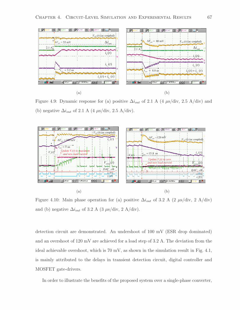
Chapter 4. Circuit-Level Simulation and Experimental Results 67
Vout (t) (ac coupled)
outi
2.1 A
)(tiL
)(tixL
)()( titixLL
!" outV
rest 3.2 us
55 mV
(a)
Vout (t) (ac coupled)
outi 2.1 A
)(tiL
)(tixL
)()( titixLL
!" outV
rest
80 mV
8.8 us
(b)
Figure 4.9: Dynamic response for (a) positive ∆iout of 2.1 A (4 µs/div, 2.5 A/div) and
(b) negative ∆iout of 2.1 A (4 µs/div, 2.5 A/div).
Vout (t) (ac coupled)
100 ! outV
5 rest
)(tiL
)(tVsense
)(tVc
clkDAC_
)(1 tc)(2 tc
Update Vc(t) to maximum
and new load current
mV
us
(a)
Vout (t) (ac coupled)
)(tiL
)(tVsense
120 ! outV
8.15 rest)(tVc
clkDAC_
)(1 tc)(2 tc
Update Vc(t) to zero
and new load current
mV
us
(b)
Figure 4.10: Main phase operation for (a) positive ∆iout of 3.2 A (2 µs/div, 2 A/div)
and (b) negative ∆iout of 3.2 A (3 µs/div, 2 A/div).
detection circuit are demonstrated. An undershoot of 100 mV (ESR drop dominated)
and an overshoot of 120 mV are achieved for a load step of 3.2 A. The deviation from the
ideal achievable overshoot, which is 70 mV, as shown in the simulation result in Fig. 4.1,
is mainly attributed to the delays in transient detection circuit, digital controller and
MOSFET gate-drivers.
In order to illustrate the benefits of the proposed system over a single-phase converter,

Chapter 4. Circuit-Level Simulation and Experimental Results 68
Vout (t) (ac coupled)
outi
3.2 A
)(tixL
)()( titixLL
!" outV
rest
1comp
foundstepload __)(3 tc)(4 tc
1st postive edge indicates load is reached
100 mV
5 us
(a)
Vout (t) (ac coupled)
outi 3.2 A
)(tixL
)()( titixLL
!" outV
rest
1comp
foundstepload __)(3 tc)(4 tc
1st negative edge indicates load
is reached
120 mV
15.8 us
(b)
Figure 4.11: Auxiliary phase and load detection circuit operations for (a) positive ∆iout
of 3.2 A (2 µs/div, 2.5 A/div) and (b) negative ∆iout of 3.2 A (3 µs/div, 2.5 A/div).
Vout (t) (ac coupled)
outi 3.2 A
)(tiL
)(tixL
)()( titixLL
!" outV
rest
120 mV
15.8 us
30 mV
5 us
(a)
Vout (t) (ac coupled)
outi 3.2 A
)(tiL
! outV
rest
220 mV
10 us
80 mV
(b)
Figure 4.12: Dynamic response of a negative ∆iout of 3.2 A for (a) proposed system (4
µs/div, 2.5 A/div) and (b) single-phase system with time-optimal control (4 µs/div, 2
A/div).
the same prototype was tested with conventional time-optimal control. The inductance in
the single-phase converter was reduced to L = 3.3 µH in order to achieve a comparable
transient response. The proposed converter is compared to the representative single
phase time-optimal control converter in Table 4.2. The proposed system offers better
steady-state output voltage ripple and transient response, as shown in Fig. 4.12.

Chapter 4. Circuit-Level Simulation and Experimental Results 69
Table 4.2: System Parameter and Performance Comparison
Parameter W/ Aux. Phase Single Phase Unit
Main Phase Inductor, L 10 3.3 µH
Main Phase Inductor DCR, DCRL 18 14 mΩ
Aux. Phase Inductor, Lx 1.5 N/A µH
Inductor Current Ripple, ∆iL 0.4 1.2 A
Steady-State Output Ripple, ∆vout 30 80 mV
∆vout for a 3.2A Negative Load Step 120 220 mV
tres for a 3.2A Negative Load Step 5 10 µs
Steady-State Eff. at full load 88.4 86.5 %
Dynamic Eff. at 10 kHz of 4.2A at 50% 85.6 82.3 %
4.3.2 Phase shedding and Mode Switching
vout (t) (ac coupled)
iout = 1 A
)(tiL
)(tixL
vout (t) is not impacted
during phase switching
Figure 4.13: Switching from the main phase to the auxiliary phase.
As discussed in Section 2.4, using the auxiliary phase can improve efficiency under
light-load conditions. This justifies the additional cost of the auxiliary phase together

Chapter 4. Circuit-Level Simulation and Experimental Results 70
vout (t) (ac coupled)
iout = 0.1 A )(tixL
Vreffsx,pfm = 50 kHz
PFM_en
Figure 4.14: Switching from PWM to PFM mode in the auxiliary phase.
vout (t) (ac coupled)
iout = 0.2 A
)(tixL
Vref
fsx,pfm = 90 kHz
Figure 4.15: Steady-state operation of PFM mode in the auxiliary phase.
with the transient improvement. To switch to the auxiliary phase without impacting
Vout, the auxiliary phase is turned on with a duty cycle such that the di/dt of the two
phases are matched. The measured waveform is shown in Fig. 4.13. The phase switching
occurs when load current is 1 A, and the auxiliary phase takes over the regulation. As
the load current continues to decrease, the auxiliary phase enters PFM operation with

Chapter 4. Circuit-Level Simulation and Experimental Results 71
200
300
400
500
600
M F
req
ue
ncy (
kH
z)
0
100
0.1 1
PF
M
Load (A)
ton = 500 ns
Figure 4.16: Measured switching frequency versus load current in PFM mode.
output voltage valley point regulation. The PWM to PFM mode switching is shown
in Fig. 4.14. The mode switching operation can be initiated either by detecting load
current level or from the sleep signal provided by the digital load. The waveforms in
PFM mode are shown in Fig. 4.15 with ton of 500 ns, and the measured relationship
between PFM switching frequency fs,pfm and the load current is shown in Fig. 4.16. The
ton was selected such that the minimum fs,pfm is 50 kHz, which occurs at the minimum
current of 0.1 A.
4.3.3 Steady-State Efficiency
The steady-state efficiency of the two systems listed in Table 4.2 are also compared to
illustrated the efficiency benefit of using a large L in the main phase. Although the
smaller 3.3 µH inductor from the same product family has a smaller DC resistance,
the proposed system with the auxiliary phase still exhibits about 2 % higher steady-state
efficiency across a large range of load, as shown in Fig. 4.17. This is due to the lower RMS
conduction losses on all the resistive components for L = 10 µH. The efficiency of running
the auxiliary phase in PWM and PFM modes are shown together with the main phase in
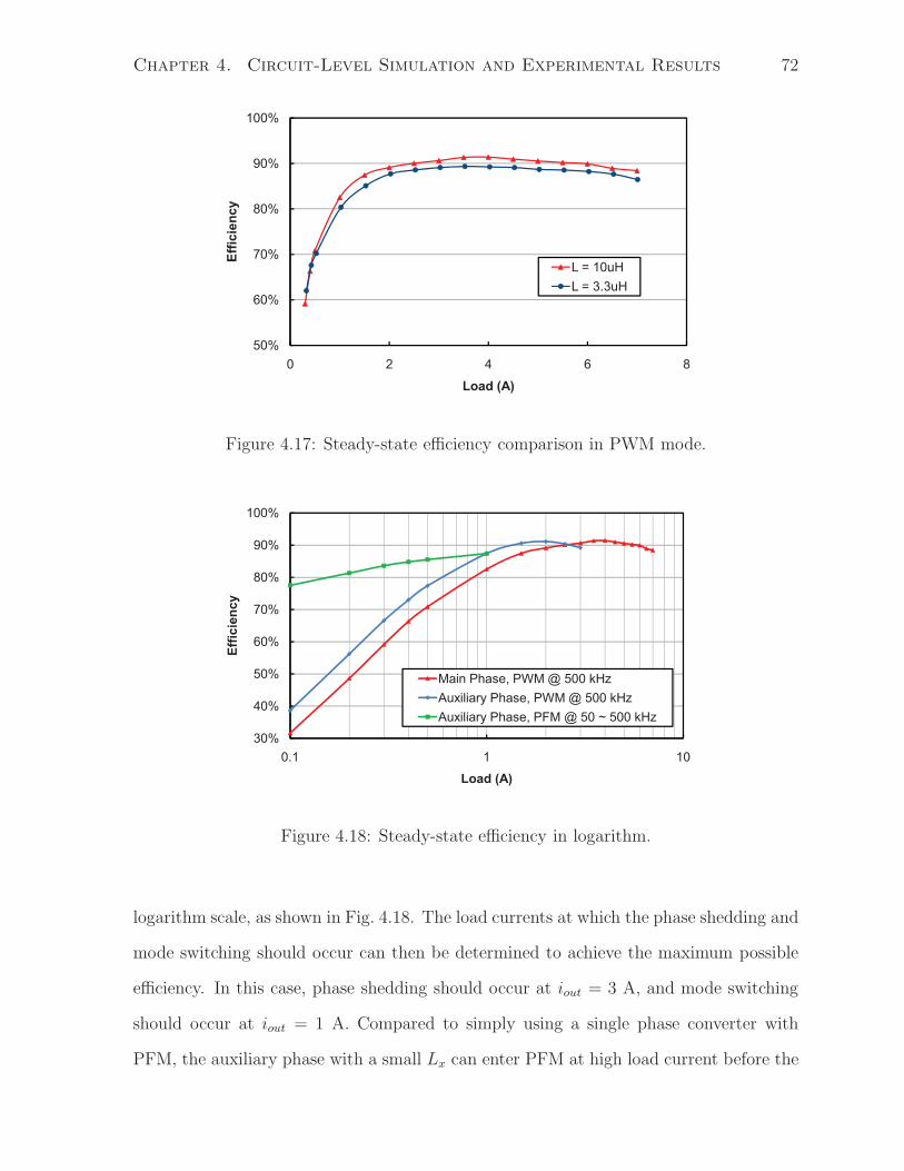
Chapter 4. Circuit-Level Simulation and Experimental Results 72
70%
80%
90%
100%
Eff
icie
ncy
L = 10uH
L 3 3 H
50%
60%
70%
80%
90%
100%
0 2 4 6 8
Eff
icie
ncy
Load (A)
L = 10uH
L = 3.3uH
Figure 4.17: Steady-state efficiency comparison in PWM mode.
50%
60%
70%
80%
90%
100%
Eff
icie
ncy
30%
40%
50%
0.1 1 10
Load (A)
Main Phase, PWM @ 500 kHz
Auxiliary Phase, PWM @ 500 kHz
Auxiliary Phase, PFM @ 50 ~ 500 kHz
Figure 4.18: Steady-state efficiency in logarithm.
logarithm scale, as shown in Fig. 4.18. The load currents at which the phase shedding and
mode switching should occur can then be determined to achieve the maximum possible
efficiency. In this case, phase shedding should occur at iout = 3 A, and mode switching
should occur at iout = 1 A. Compared to simply using a single phase converter with
PFM, the auxiliary phase with a small Lx can enter PFM at high load current before the

Chapter 4. Circuit-Level Simulation and Experimental Results 73
70%
80%
90%
100%
Eff
icie
ncy
PFM in Aux. Phase
PWM in Aux. Phase
PWM in Main Phase
PFM PWM
50%
60%
0.1 1 10
Load (A)
Proposed System with Auxiliary Phase
Representative Single Phase System
PFM
Figure 4.19: Full range steady-state efficiency comparison.
efficiency curve starts to fall. Also with the same ton, the PFM switching frequency scales
down with load current much faster with the proposed auxiliary phase. The achieved
overall efficiency with the proposed system is shown in Fig. 4.19, and the efficiency of the
single phase converter running in PFM is also plotted with the same PFM frequency and
load current relation. The proposed system exhibits as large as 10 % higher efficiency
when load current is under 0.5 A.
4.3.4 Dynamic Efficiency
Although the auxiliary phase can boost the transient response and also improve the
steady-state efficiency, the switching losses increase when the auxiliary phase is temporar-
ily activated during large load-steps. This negatively impacts the dynamic efficiency. To
quantify this effect, the proposed and the representative single-phase converters are op-
erated under the same conservative dynamic load conditions. Experimental waveforms
under 1 A to 5.2 A steps at 10 kHz are shown in Fig. 4.20. The comparison is performed
at a load step frequency from 10 kHz down to 100 Hz, with 2.1 A and 4.2 A load steps
(both at 50 % duty ratio). The dynamic efficiency is plotted in Fig. 4.21. A maximum of
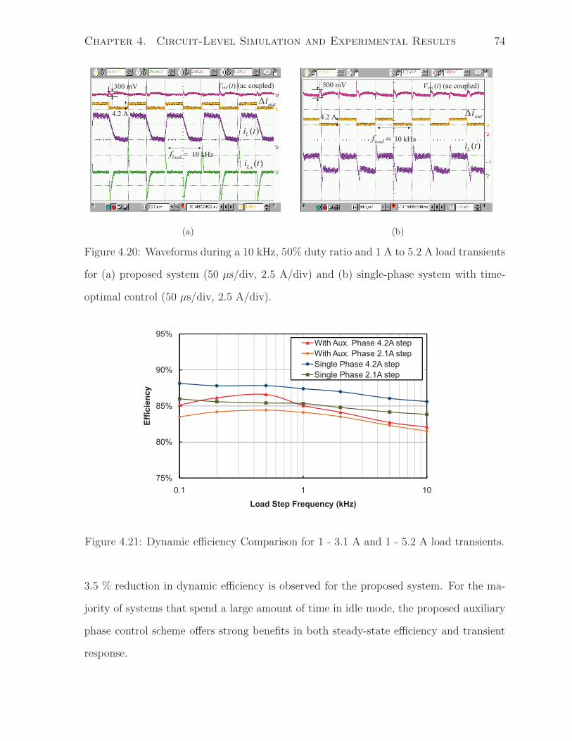
Chapter 4. Circuit-Level Simulation and Experimental Results 74
Vout (t) (ac coupled)
outi
4.2 A
)(tiL
loadf 10 kHz
300 mV
)(tixL
(a)
Vout (t) (ac coupled)
outi 4.2 A
)(tiL
loadf 10 kHz
500 mV
(b)
Figure 4.20: Waveforms during a 10 kHz, 50% duty ratio and 1 A to 5.2 A load transients
for (a) proposed system (50 µs/div, 2.5 A/div) and (b) single-phase system with time-
optimal control (50 µs/div, 2.5 A/div).
80%
85%
90%
95%
Eff
icie
ncy
With Aux. Phase 4.2A step
With Aux. Phase 2.1A step
Single Phase 4.2A step
Single Phase 2.1A step
75%
80%
85%
90%
95%
0.1 1 10
Eff
icie
ncy
Load Step Frequency (kHz)
With Aux. Phase 4.2A step
With Aux. Phase 2.1A step
Single Phase 4.2A step
Single Phase 2.1A step
Figure 4.21: Dynamic efficiency Comparison for 1 - 3.1 A and 1 - 5.2 A load transients.
3.5 % reduction in dynamic efficiency is observed for the proposed system. For the ma-
jority of systems that spend a large amount of time in idle mode, the proposed auxiliary
phase control scheme offers strong benefits in both steady-state efficiency and transient
response.

References
[1] W. Ng, J. Wang, K. Ng, A. Prodic, T. Kawashima, M. Sasaki, and H. Nishio, “Dig-
itally controlled integrated dc-dc converters with fast transient response,” in IEEE
International Symposium on Radio-Frequency Integration Technology, 2009. RFIT
2009, pp. 335–338, Jan. 2009.
[2] E. Meyer, D. Wang, L. Jia, and Y.-F. Liu, “Digital charge balance controller with
an auxiliary circuit for superior unloading transient performance of buck converters,”
in Twenty-Fifth Annual IEEE Applied Power Electronics Conference and Exposition
(APEC), 2010, pp. 124–131, Feb. 2010.
[3] E. Meyer, Z. Zhang, and Y.-F. Liu, “Controlled auxiliary circuit to improve the
unloading transient response of buck converters,” IEEE Transactions on Power Elec-
tronics, vol. 25, pp. 806–819, Apr. 2010.
[4] Z. Zhao and A. Prodic, “Continuous-time digital controller for high-frequency dc-dc
converters,” IEEE Transactions on Power Electronics, vol. 23, pp. 564–573, Mar.
2008.
[5] “Spartan-3E FPGA Family: Data Sheet.” Xilinx, Inc.
[6] “Spartan-3E Starter Kit Board User Guide.” Digilent, Inc.
75

Chapter 5
Conclusions
5.1 Thesis Summary and Contributions
The focus of this work is to address the ever-growing demands of fast transient response
and high efficiency PoL converters. A CPM buck converter with digital adaptive slope
control (DASC) in the auxiliary phase is developed. Through theoretical calculation,
mixed-signal simulation and experimental verification, the DASC scheme is verified to
actively adjust the charge balancing rate such that the undesired voltage deviations ob-
served in the existing techniques are eliminated, and the optimal response is maintained
for both positive and negative load steps with various current slew rates. Moreover, the
efficiency and transient response trade-off is decoupled to provide designers with an addi-
tional degree of freedom in the design optimization process. Neither the control scheme
nor the load detection circuit require oversampling of vout(t), which greatly simplifies
the controller design. A calibration scheme, taking the advantage of the direct access
to inductor current in CPM control, is also presented to calibrate the controller against
the inductance variance due to manufacture tolerances, which is essential in any precise
charge balancing controller designs.
The technique is verified on a 500 kHz, 10 V to 2.5 V current-mode buck converter
76

Chapter 5. Conclusions 77
prototype. The ideal transient improvement on ∆vout, with the proposed system, is
(1+L/Lx) = 7.7×, compared to a single-phase system with the same L and Cout. Equiv-
alently, the proposed system requires 7.7× less Cout to maintain the same dynamic re-
sponse, compare to the time-optimal control technique in a single phase system. The
settling time tres is reduced by (1 +√
Vg−Vout
Vout+ 1) = 3× for a positive load step, and
(1+√
Vout
Vg−Vout+ 1) = 2.15× for a negative load step. Further transient improvement can
be achieved with a smaller Lx using the same technique.
Since the main phase with a large inductance L is operated during steady-state,
the steady-state output voltage ripple is lower. Also the RMS losses are also lower
so that the heavy-load steady-state efficiency is about 2 % higher, compared to the
representative single phase converter. Furthermore, since the auxiliary phase has smaller
power MOSFETs which have smaller gate charge Qg, using it in PFM mode provides
about 10 % light-load efficiency improvement. The phase shedding and mode switching
techniques are presented. The efficiency impact of the auxiliary phase operation during
transient is also presented. All of above are supported by simulation and experimental
results.
The auxiliary phase with the DASC scheme greatly improves the converter’s dynamic
response, and the cost of it is not comparable to the main phase, since it only operates
during transient and small power devices are used. The DC current rating of the auxiliary
phase is 25 % of the rating of main phase, and the size of the auxiliary phase is also only
25 % of the size of the main phase. The efficiency improvement as a result of using the
auxiliary phase under both heavy and light load conditions further justifies the additional
cost. This research work has led to two conference publications [1, 2], and a journal
publication [3].

Chapter 5. Conclusions 78
5.2 Future Work
The proposed control scheme and the auxiliary phase structure can be expanded to
converters at different power levels:
1. Multiphase VRM: In desktop and server systems, multiphase VRMs are used
to provide power up to hundreds of watts. Each phase is commonly implemented
with the same power components to equally split the total power. The proposed
auxiliary phase technique can be easily incorporated by considering the sum of
the other phases as one large phase. And it is possible to incorporate adaptive-
voltage-positioning (AVP) into the charge balancing calculation, which is commonly
required in VRM designs [4].
2. High Frequency Integrated Converter: In sub-1 W applications, high fre-
quency integrated switching regulator still has efficiency advantage over LDOs or
switched capacitor regulators, but the disadvantage is that an off-chip inductor is
required. However, as the switching frequency increases, the value of the reactive
components L and C can be reduced, which makes them possible to be integrated
on-chip. The auxiliary phase technique has been developed for integrated con-
verter with on-chip main and auxiliary power MOSFETs [5,6]. With the proposed
technique in this work, the proposed auxiliary phase has Lx almost an order of mag-
nitude smaller than L, therefore the auxiliary phase including Lx can be potentially
fully integrated on-chip.
3. Other Converter Topologies: The same concept of the auxiliary phase archi-
tecture can be used to improve dynamic response and efficiency for other converter
topologies. For a boost converter, for example, the existence of the right-half-plane
(RHP) zero limits the control bandwidth. Some nonlinear control techniques have
been developed to improve the transient response for a boost converter [7, 8]. The
improvement however, is moderate compared to the significant improvement pro-

Chapter 5. Conclusions 79
vided by the auxiliary phase for the buck topology, as illustrated in this work. The
auxiliary phase can be operated either in buck or boost mode. It is therefore pos-
sible to extend the proposed technique to improve dynamic response for the boost
topology, with slight modification in the timing of charge balancing control.

References
[1] Y. Wen and O. Trescases, “Non-linear control of current-mode buck converter with
an optimally scaled auxiliary phase,” in IEEE International Conference on Industrial
Technology (ICIT), 2010, pp. 783–788, Mar. 2010.
[2] Y. Wen and O. Trescases, “Dc-dc converter with digital adaptive slope control in
auxiliary phase to achieve optimal transient response,” in Twenty-Sixth Annual IEEE
Applied Power Electronics Conference and Exposition (APEC), 2011, pp. 331–337,
Mar. 2011.
[3] Y. Wen and O. Trescases, “Dc-dc converter with digital adaptive slope control in aux-
iliary phase and self-calibration for optimal transient response,” IEEE Transactions
on Power Electronics, 2011, submitted.
[4] E. Meyer, D. Wang, L. Jia, and Y.-F. Liu, “Digital charge balance controller with
an auxiliary circuit for superior unloading transient performance of buck converters,”
in Twenty-Fifth Annual IEEE Applied Power Electronics Conference and Exposition
(APEC), 2010, pp. 124–131, Feb. 2010.
[5] J. Wang, K. Ng, T. Kawashima, M. Sasaki, H. Nishio, A. Prodic, and W. Ng, “A digi-
tally controlled integrated dc-dc converter with transient suppression,” in 22nd Inter-
national Symposium on Power Semiconductor Devices IC’s (ISPSD), 2010, pp. 277–
280, Jun. 2010.
80

REFERENCES 81
[6] W. Ng, J. Wang, K. Ng, A. Prodic, T. Kawashima, M. Sasaki, and H. Nishio, “Dig-
itally controlled integrated dc-dc converters with fast transient response,” in IEEE
International Symposium on Radio-Frequency Integration Technology, 2009. RFIT
2009, pp. 335–338, Jan. 2009.
[7] J.-C. Tsai, C.-L. Chen, Y.-H. Lee, H.-Y. Yang, M.-S. Hsu, and K.-H. Chen, “Mod-
ified hysteretic current control (MHCC) for improving transient response of boost
converter,” IEEE Transactions on Circuits and Systems, no. 99, pp. 1–13, 2011.
[8] C.-Y. Hsieh and K.-H. Chen, “Boost dc-dc converter with fast reference tracking
(FRT) and charge-recycling (CR) techniques for high-efficiency and low-cost LED
driver,” IEEE Journal of Solid-State Circuits, vol. 44, pp. 2568–2580, Sep. 2009.


![DC-DC Converter with Coupled Inductor and Multiplier Cells ... · gain is also improved by using a parallel input output series boost converter [13]. This DC-DC Converter makes use](https://img.dokumen.tips/doc/110x75/5f0b56627e708231d43004bb/dc-dc-converter-with-coupled-inductor-and-multiplier-cells-gain-is-also-improved.jpg)