Embed Size (px)
Citation preview

HardCopy IV Device Handbook, Volume 4: DatasheetDecember 2011
HIV54001-2.1
Subscribe
© 2011 Altera Corporation. All rights reserved. ALTERA, ARRIA, CYCLONE, HARDCOPY, MAX, MEGACORE, NIOS, QUARTUS and STRATIX are Reg. U.S. Pat. & Tm. Off. and/or trademarks of Altera Corporation in the U.S. and other countries. All other trademarks and service marks are the property of their respective holders as described at www.altera.com/common/legal.html. Altera warrants performance of its semiconductor products to current specifications in accordance with Altera’s standard warranty, but reserves the right to make changes to any products and services at any time without notice. Altera assumes no responsibility or liability arising out of the application or use of any information, product, or service described herein except as expressly agreed to in writing by Altera. Altera customers are advised to obtain the latest version of device specifications before relying on any published information and before placing orders for products or services.
1. DC and Switching Characteristics ofHardCopy IV Devices
Electrical CharacteristicsThis chapter covers the electrical characteristics for HardCopy® IV devices.
Operating ConditionsWhen implementing HardCopy IV devices in a system, the system rates the devices according to a set of defined parameters. To maintain the highest possible performance and reliability, consider the operating requirements described in this chapter. HardCopy IV devices are not speed binned because HardCopy IV devices function at a target frequency based on timing constraints. Altera offers HardCopy IV devices that support applications in commercial or industrial grade temperatures.
Absolute Maximum RatingsAbsolute maximum ratings define the maximum operating conditions for HardCopy IV devices. Experiments with the device and theoretical modeling of breakdown and damage mechanisms provide these values. These conditions do not imply the functional operation of the device.
Table 1–1 lists the absolute maximum ratings for a HardCopy IV device.
1 Conditions other than those listed in Table 1–1 and Table 1–3 may cause permanent damage to the device. Additionally, device operation at the absolute maximum ratings for extended periods of time may have adverse effects on the device.
Table 1–1. HardCopy IV Device Absolute Maximum Ratings (Part 1 of 2) (Note 1)
Symbol Description Minimum Maximum Unit
VCC Core voltage and periphery circuitry power supply –0.5 1.35 V
VCCPT (2) Power supply for programmable power technology — — V
VCCPGM Configuration pins power supply –0.5 3.75 V
VCCAUX Power supply for temperature sensing diode and POR –0.5 3.75 V
VCCBAT (3) Battery back-up power supply for design security volatile key register — — V
VCCPD I/O predriver power supply –0.5 3.75 V
VCCIO I/O power supply –0.5 3.9 V
VCC_CLKIN Differential clock input power supply –0.5 3.75 V
VCCD_PLL Phase-locked loop (PLL) digital power supply –0.5 1.35 V
VCCA_PLL PLL analog power supply –0.5 3.75 V
VI DC input voltage –0.5 4.0 V

1–2 Chapter 1: DC and Switching Characteristics of HardCopy IV DevicesElectrical Characteristics
HardCopy IV Device Handbook, Volume 4: Datasheet December 2011 Altera Corporation
Table 1–2 lists the power supply absolute maximum ratings for HardCopy IV GX transceiver.
IOUT DC output current per pin –25 40 mA
TJ Operating junction temperature –55 125 C
TSTG Storage temperature (No bias) –65 150 C
Notes to Table 1–1:
(1) Supply voltage specifications apply to voltage readings taken at the device pins and not the power supply.(2) HardCopy IV devices do not require programmable power technology.(3) HardCopy IV devices do not use this power supply.
Table 1–1. HardCopy IV Device Absolute Maximum Ratings (Part 2 of 2) (Note 1)
Symbol Description Minimum Maximum Unit
Table 1–2. HardCopy IV GX Transceiver Power Supply Absolute Maximum Ratings
Symbol Description Minimum Maximum Unit
VCCA_L Transceiver high voltage power (left side) –0.5 3.75 V
VCCA_R Transceiver high voltage power (right side) –0.5 3.75 V
VCCHIP_L Transceiver hard IP digital power (right side) –0.5 1.35 V
VCCHIP_R Transceiver hard IP digital power (left side) –0.5 1.35 V
VCCR_L Receiver power (left side) –0.5 1.35 V
VCCR_R Receiver power (right side) –0.5 1.35 V
VCCT_L Transmitter power (left side) –0.5 1.35 V
VCCT_R Transmitter power (right side) –0.5 1.35 V
VCCL_GXBLn (1) Transceiver clock power (left side) –0.5 1.35 V
VCCL_GXBRn (1) Transceiver clock power (right side) –0.5 1.35 V
VCCH_GXBLn (1) Transmitter output buffer power (left side) –0.5 1.65 V
VCCH_GXBRn (1) Transmitter output buffer power (right side) –0.5 1.65 V
Note to Table 1–2:
(1) The VCCH and VCCL powers are per transceiver block.

Chapter 1: DC and Switching Characteristics of HardCopy IV Devices 1–3Electrical Characteristics
December 2011 Altera Corporation HardCopy IV Device Handbook, Volume 4: Datasheet
Maximum Allowed Overshoot or Undershoot Voltage
Table 1–3 lists the maximum allowed input overshoot voltage and the duration of the overshoot voltage as a percentage of device lifetime. The maximum allowed overshoot duration is a percentage of high-time over the lifetime of the device. A DC signal is equivalent to 100% duty cycle.
During transitions, input signals may overshoot to the voltage shown in Table 1–3 and undershoot to –2.0 V for input currents less than 100 mA and periods shorter than 20 ns.
Table 1–3. Maximum Allowed Overshoot During Transitions
Symbol Description Condition Overshoot Duration as Percentage of High Time Unit
Vi (AC) AC input voltage
4.0 V 100.000 %
4.05 V 79.330 %
4.1 V 46.270 %
4.15 V 27.030 %
4.2 V 15.800 %
4.25 V 9.240 %
4.3 V 5.410 %
4.35 V 3.160 %
4.4 V 1.850 %
4.45 V 1.080 %
4.5 V 0.630 %
4.55 V 0.370 %
4.6 V 0.220 %
4.65 V 0.130 %
4.7 V 0.074 %
4.75 V 0.043 %
4.8 V 0.025 %
4.85 V 0.015 %

Chapter 1: DC and Switching Characteristics of HardCopy IV Devices 1–4Electrical Characteristics
December 2011 Altera Corporation HardCopy IV Device Handbook, Volume 4: Datasheet
Figure 1–1 shows the methodology to determine overshoot duration. The color red shows the overshoot voltage and is present at the HardCopy IV pin, up to 4.1 V. In Table 1–3, for an overshoot of up to 4.1 V, the percentage of high time for overshoot is greater than 3.15 V can be as high as 46% over an 11.4 year period. The percentage of high time is (Δ T/T) × 100. This 11.4 year period assumes that you turned on the device with 100% I/O toggle rate and 50% duty cycle signal. Lifetimes increase for lower I/O toggle rates and situations in which the device is in an idle state.
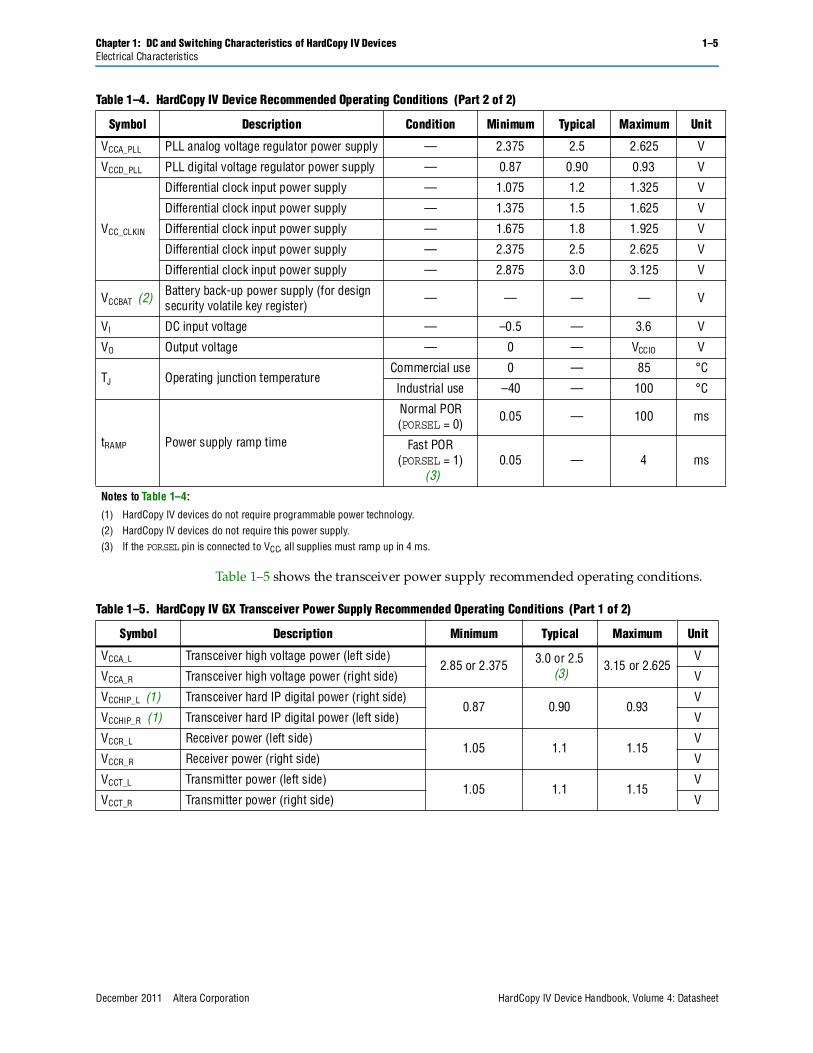
Recommended Operating ConditionsThis section lists the functional operation limits for AC and DC parameters for HardCopy IV devices. Table 1–4 shows the steady-state voltage and current values expected from HardCopy IV devices. All supplies must reach their full-rail values in tRAMP maximum monotonically.
Figure 1–1. Overshoot Duration
3.0 V3.15 V
4.1 V
T
ΔT
Table 1–4. HardCopy IV Device Recommended Operating Conditions (Part 1 of 2)
Symbol Description Condition Minimum Typical Maximum Unit
VCCCore voltage and periphery circuitry power supply
— 0.87 0.90 0.93 V
VCCPT (1) Power supply for programmable power technology
— — — — V
VCCAUXPower supply for the temperature sensing diode and POR
— 2.375 2.5 2.625 V
VCCPD I/O predriver (3.0 V) power supply — 2.85 3 3.15 V
I/O predriver (2.5 V) power supply — 2.375 2.5 2.625 V
VCCIO
I/O buffers (3.0 V) power supply — 2.85 3 3.15 V
I/O buffers (2.5 V) power supply — 2.375 2.5 2.625 V
I/O buffers (1.8 V) power supply — 1.71 1.8 1.89 V
I/O buffers (1.5 V) power supply — 1.425 1.5 1.575 V
I/O buffers (1.2 V) power supply — 1.14 1.2 1.26 V
VCCPGM
Configuration pins (3.0 V) power supply — 2.85 3 3.15 V
Configuration pins (2.5 V) power supply — 2.375 2.5 2.625 V
Configuration pins (1.8 V) power supply — 1.71 1.8 1.89 V
Chapter 1: DC and Switching Characteristics of HardCopy IV Devices 1–5Electrical Characteristics
December 2011 Altera Corporation HardCopy IV Device Handbook, Volume 4: Datasheet
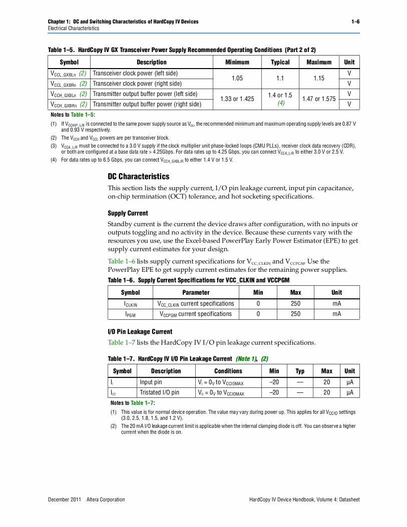
Table 1–5 shows the transceiver power supply recommended operating conditions.
VCCA_PLL PLL analog voltage regulator power supply — 2.375 2.5 2.625 V
VCCD_PLL PLL digital voltage regulator power supply — 0.87 0.90 0.93 V
VCC_CLKIN
Differential clock input power supply — 1.075 1.2 1.325 V
Differential clock input power supply — 1.375 1.5 1.625 V
Differential clock input power supply — 1.675 1.8 1.925 V
Differential clock input power supply — 2.375 2.5 2.625 V
Differential clock input power supply — 2.875 3.0 3.125 V
VCCBAT (2) Battery back-up power supply (for design security volatile key register)
— — — — V
VI DC input voltage — –0.5 — 3.6 V
VO Output voltage — 0 — VCCIO V
TJ Operating junction temperatureCommercial use 0 — 85 °C
Industrial use –40 — 100 °C
tRAMP Power supply ramp time
Normal POR (PORSEL = 0)
0.05 — 100 ms
Fast POR (PORSEL = 1)
(3)0.05 — 4 ms
Notes to Table 1–4:
(1) HardCopy IV devices do not require programmable power technology.(2) HardCopy IV devices do not require this power supply.(3) If the PORSEL pin is connected to VCC, all supplies must ramp up in 4 ms.
Table 1–4. HardCopy IV Device Recommended Operating Conditions (Part 2 of 2)
Symbol Description Condition Minimum Typical Maximum Unit
Table 1–5. HardCopy IV GX Transceiver Power Supply Recommended Operating Conditions (Part 1 of 2)
Symbol Description Minimum Typical Maximum Unit
VCCA_L Transceiver high voltage power (left side)2.85 or 2.375 3.0 or 2.5
(3)3.15 or 2.625
V
VCCA_R Transceiver high voltage power (right side) V
VCCHIP_L (1) Transceiver hard IP digital power (right side)0.87 0.90 0.93
V
VCCHIP_R (1) Transceiver hard IP digital power (left side) V
VCCR_L Receiver power (left side)1.05 1.1 1.15
V
VCCR_R Receiver power (right side) V
VCCT_L Transmitter power (left side)1.05 1.1 1.15
V
VCCT_R Transmitter power (right side) V
Chapter 1: DC and Switching Characteristics of HardCopy IV Devices 1–6Electrical Characteristics
December 2011 Altera Corporation HardCopy IV Device Handbook, Volume 4: Datasheet
DC CharacteristicsThis section lists the supply current, I/O pin leakage current, input pin capacitance, on-chip termination (OCT) tolerance, and hot socketing specifications.
Supply Current
Standby current is the current the device draws after configuration, with no inputs or outputs toggling and no activity in the device. Because these currents vary with the resources you use, use the Excel-based PowerPlay Early Power Estimator (EPE) to get supply current estimates for your design.
Table 1–6 lists supply current specifications for VCC_CLKIN and VCCPGM. Use the PowerPlay EPE to get supply current estimates for the remaining power supplies.
I/O Pin Leakage Current
Table 1–7 lists the HardCopy IV I/O pin leakage current specifications.
VCCL_GXBLn (2) Transceiver clock power (left side)1.05 1.1 1.15
V
VCCL_GXBRn (2) Transceiver clock power (right side) V
VCCH_GXBLn (2) Transmitter output buffer power (left side)1.33 or 1.425 1.4 or 1.5
(4)1.47 or 1.575
V
VCCH_GXBRn (2) Transmitter output buffer power (right side) V
Notes to Table 1–5:
(1) If VCCHIP_L/R is connected to the same power supply source as Vcc, the recommended minimum and maximum operating supply levels are 0.87 V and 0.93 V respectively.
(2) The VCCH and VCCL powers are per transceiver block.(3) VCCA_L/R must be connected to a 3.0 V supply if the clock multiplier unit phase-locked loops (CMU PLLs), receiver clock data recovery (CDR),
or both are configured at a base data rate > 4.25Gbps. For data rates up to 4.25 Gbps, you can connect VCCA_L/R to either 3.0 V or 2.5 V.(4) For data rates up to 6.5 Gbps, you can connect VCCH_GXBL/R to either 1.4 V or 1.5 V.
Table 1–5. HardCopy IV GX Transceiver Power Supply Recommended Operating Conditions (Part 2 of 2)
Symbol Description Minimum Typical Maximum Unit
Table 1–6. Supply Current Specifications for VCC_CLKIN and VCCPGM
Symbol Parameter Min Max Unit
ICLKIN VCC_CLKIN current specifications 0 250 mA
IPGM VCCPGM current specifications 0 250 mA
Table 1–7. HardCopy IV I/O Pin Leakage Current (Note 1), (2)
Symbol Description Conditions Min Typ Max Unit
II Input pin VI = 0V to VCCIOMAX –20 — 20 µA
IOZ Tristated I/O pin VO = 0V to VCCIOMAX –20 — 20 µA
Notes to Table 1–7:
(1) This value is for normal device operation. The value may vary during power up. This applies for all VCCIO settings (3.0, 2.5, 1.8, 1.5, and 1.2 V).
(2) The 20 mA I/O leakage current limit is applicable when the internal clamping diode is off. You can observe a higher current when the diode is on.

Chapter 1: DC and Switching Characteristics of HardCopy IV Devices 1–7Electrical Characteristics
December 2011 Altera Corporation HardCopy IV Device Handbook, Volume 4: Datasheet
Bus Hold Specifications
Table 1–8 lists the HardCopy IV bus hold specifications
OCT Specifications
If you enabled OCT calibration, calibration is automatically performed at power up for I/Os connected to the calibration block. Table 1–9 lists the HardCopy IV OCT calibration block accuracy specifications.
Table 1–8. Bus Hold Parameters
Parameter Symbol Condition
VCCIO
Unit1.2 V 1.5 V 1.8 V 2.5 V 3.0 V
Min Max Max Min Max Min Min Max Max Max
Low sustaining current
ISUSLVIN > VIL
(maximum)22.5 — 25.0 — 30.0 — 50.0 — 70.0 — μA
High sustaining current
ISUSHVIN < VIH
(minimum)–22.5 — –25.0 — –30.0 — –50.0 — –70.0 — μA
Low overdrive current
IODL 0V < VIN < VCCIO — 120 — 160 — 200 — 300 — 500 μA
High overdrive current
IODH 0V < VIN < VCCIO — –120 — –160 — –200 — –300 — –500 μA
Bus-hold trip point
VTRIP — 0.45 0.95 0.50 1.00 0.68 1.07 0.70 1.70 0.80 2.00 V
Table 1–9. HardCopy IV OCT With Calibration Specification for I/Os (Note 1)
Symbol Description Conditions Calibration Accuracy
Unit
25-Ω RS 3.0/2.5/1.8/1.5/1.2 (2)
Internal series termination with calibration (25-Ω setting)
VCCIO = 3.0/2.5/1.8/1.5/1.2 V ±8 %
50-Ω RS 3.0/2.5/1.8/1.5/1.2 Internal series termination with calibration (50-Ω setting)
VCCIO = 3.0/2.5/1.8/1.5/1.2 V ±8 %
50-Ω RT 2.5/1.8/1.5/1.2 Internal parallel termination with calibration (50-Ω setting)
VCCIO = 2.5/1.8/1.5/1.2 V ±10 %
25-Ω, 25-Ω, and 25-Ω RS 3.0/2.5/1.8/1.5/1.2 (3)
Expanded range for internal series termination with calibration (20-Ω, 40-Ω and 60-Ω RS settings)
VCCIO = 3.0/2.5/1.8/1.5/1.2 V ±10 %
25-Ω RS_left_shiftInternal left shift series termination with calibration (25-Ω RS_left_shift setting)
VCCIO = 3.0/2.5/1.8/1.5/1.2 V ±10 %
Notes to Table 1–9:
(1) OCT calibration accuracy is valid at the time of calibration only.(2) 25-Ω RS not supported for 1.5 V and 1.2 V in Row I/O.(3) 20-Ω RS not supported for 1.5 V and 1.2 V in Row I/O.
Chapter 1: DC and Switching Characteristics of HardCopy IV Devices 1–8Electrical Characteristics
December 2011 Altera Corporation HardCopy IV Device Handbook, Volume 4: Datasheet
The calibration accuracy for calibrated series and parallel OCTs are applicable at the moment of calibration. If the voltage or temperature changes, the termination resistance value varies. Table 1–10 lists the resistance tolerance for HardCopy IV OCT.
Table 1–11 lists OCT variation with temperature and voltage after power-up calibration. Use Table 1–11 and Equation 1–1 to determine the OCT variation when voltage and temperature vary after power-up calibration.
Table 1–10. I/O OCT Resistance Tolerance
Symbol Description
Resistance Tolerance
Commercial Max
Industrial Max Unit
25-Ω RS 3.0/2.5 Internal series termination without calibration (25-Ω setting) VCCIO = 3.0/2.5 V
±40 %
25-Ω RS 1.8/1.5 Internal series termination without calibration (25-Ω setting) VCCIO = 1.8/1.5 V ±40 %
25-Ω RS 1.2 Internal series termination without calibration (25-Ω setting) VCCIO = 1.2 V ±50 %
50-Ω RS 3.0/2.5 Internal series termination without calibration (50-Ω setting) VCCIO = 3.0/2.5 V ±40 %
50-Ω RS 1.8/1.5 Internal series termination without calibration (50-Ω setting) VCCIO = 1.8/1.5 V ±40 %
50-Ω RS 1.2 Internal series termination without calibration (50-Ω setting) VCCIO = 1.2 V ±50 %
Equation 1–1. OCT Variation Without Recalibration (Note 1), (2), (3), (4), (5), (6)
Notes to Equation 1–1:(1) ROCT value calculated from Equation 1–1 shows the range of OCT resistance with the variation of temperature and
VCCIO.(2) RSCAL is the OCT resistance value at power-up. (3) ΔT is the variation of temperature with respect to the temperature at power-up.(4) ΔV is the variation of voltage with respect to the VCCIO at power-up. (5) dR/dT is the percentage change of RSCAL with temperature.(6) dR/dV is the percentage change of RSCAL with voltage.
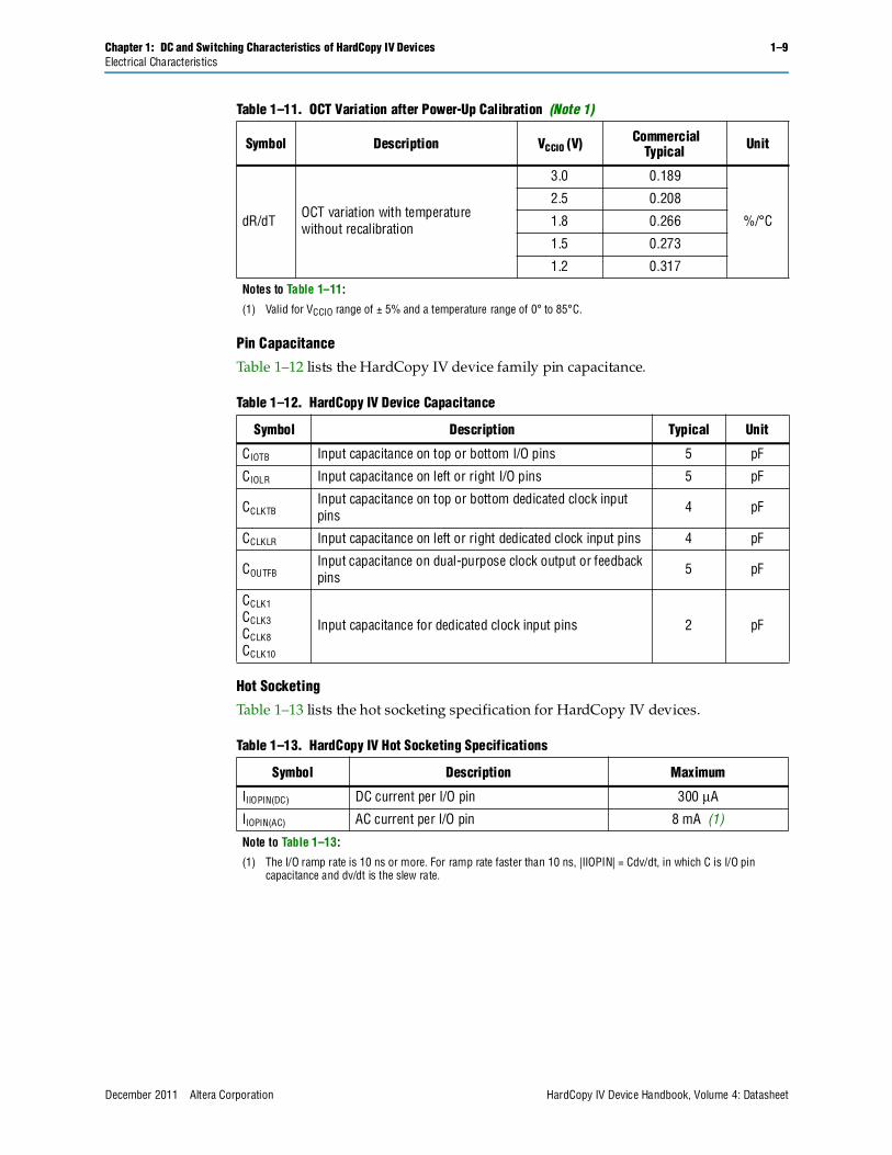
Table 1–11. OCT Variation after Power-Up Calibration (Note 1)
Symbol Description VCCIO (V) Commercial Typical Unit
dR/dVOCT variation with voltage without recalibration
3.0 0.0297
%/mV
2.5 0.0344
1.8 0.0499
1.5 0.0744
1.2 0.1241
ROCT RSCA L 1 dRdT------- ΔT× dR
dV------- ΔV× ±+
=
Chapter 1: DC and Switching Characteristics of HardCopy IV Devices 1–9Electrical Characteristics
December 2011 Altera Corporation HardCopy IV Device Handbook, Volume 4: Datasheet
Pin Capacitance
Table 1–12 lists the HardCopy IV device family pin capacitance.
Hot Socketing
Table 1–13 lists the hot socketing specification for HardCopy IV devices.
dR/dTOCT variation with temperature without recalibration
3.0 0.189
%/°C
2.5 0.208
1.8 0.266
1.5 0.273
1.2 0.317
Notes to Table 1–11:
(1) Valid for VCCIO range of ± 5% and a temperature range of 0° to 85°C.
Table 1–12. HardCopy IV Device Capacitance
Symbol Description Typical Unit
CIOTB Input capacitance on top or bottom I/O pins 5 pF
CIOLR Input capacitance on left or right I/O pins 5 pF
CCLKTBInput capacitance on top or bottom dedicated clock input pins
4 pF
CCLKLR Input capacitance on left or right dedicated clock input pins 4 pF
COUTFBInput capacitance on dual-purpose clock output or feedback pins
5 pF
CCLK1CCLK3CCLK8 CCLK10
Input capacitance for dedicated clock input pins 2 pF
Table 1–13. HardCopy IV Hot Socketing Specifications
Symbol Description Maximum
IIIOPIN(DC) DC current per I/O pin 300 μA
IIOPIN(AC) AC current per I/O pin 8 mA (1)
Note to Table 1–13:
(1) The I/O ramp rate is 10 ns or more. For ramp rate faster than 10 ns, |IIOPIN| = Cdv/dt, in which C is I/O pin capacitance and dv/dt is the slew rate.
Table 1–11. OCT Variation after Power-Up Calibration (Note 1)
Symbol Description VCCIO (V) Commercial Typical Unit

Chapter 1: DC and Switching Characteristics of HardCopy IV Devices 1–10Electrical Characteristics
December 2011 Altera Corporation HardCopy IV Device Handbook, Volume 4: Datasheet
Internal Weak Pull-Up Resistor
Table 1–14 lists the weak pull-up resistor values for HardCopy IV devices.
I/O Standard SpecificationsTable 1–15 through Table 1–20 list input voltage (VIH and VIL), output voltage (VOH and VOL), and current drive characteristics (IOH and IOL) for various I/O standards supported by HardCopy IV devices. These tables also show the HardCopy IV device family I/O standard specifications. For an explanation of terms used in Table 1–15 through Table 1–20, refer to the “Glossary” on page 1–35. VOL and VOH values are valid at the corresponding IOH and IOL, respectively.
Table 1–14. HardCopy IV Internal Weak Pull-Up Resistor (1), (2)
Symbol Parameter Conditions Typ Unit
RPU
Value of I/O pin pull-up resistor before and during configuration, as well as user mode if the programmable pull-up resistor option is enabled.
VCCIO = 3.0 V ± 5% (3) 25 kΩ
VCCIO = 2.5 V ± 5% (3) 25 kΩ
VCCIO = 1.8 V ± 5% (3) 25 kΩ
VCCIO = 1.5 V ± 5% (3) 25 kΩ
VCCIO = 1.2 V ± 5% (3) 25 kΩ
Notes to Table 1–14:
(1) All I/O pins have an option to enable weak pull-up except test and JTAG pins.(2) The internal weak pull-down feature is only available for JTAG TCK pin. The typical value for this internal weak pull-down resistor is around 25k.(3) Pin pull-up resistance values may be lower if an external source drives the pin higher than VCCIO.
Table 1–15. Single-Ended I/O Standards
I/O StandardVCCIO (V) VIL (V) VIH (V) VOL (V) VOH (V) IOL
(mA)IOH
(mA)Min Typ Max Min Max Min Max Max Min
3.3-V LVTTL 2.85 3 3.15 –0.3 0.8 1.7 3.6 0.4 2.4 2 –2
3.3-V LVCMOS 2.85 3 3.15 –0.3 0.8 1.7 3.6 0.2 VCCIO - 0.2 0.1 –0.1
2.5-V LVTTL/LVCMOS
2.375 2.5 2.625 –0.3 0.7 1.7 3.6
0.2 2.1 0.1 –0.1
0.4 2 1 –1
0.7 1.7 2 –2
1.8-V LVTTL/LVCMOS 1.71 1.8 1.89 –0.3 0.35 * VCCIO 0.65 * VCCIO VCCIO + 0.3 0.45 VCCIO - 0.45 2 –2
1.5-V LVTTL/LVCMOS 1.425 1.5 1.575 –0.3 0.35 * VCCIO 0.65 * VCCIO VCCIO + 0.3 0.25 * VCCIO 0.75 * VCCIO 2 –2
1.2-V LVTTL/LVCMOS 1.14 1.2 1.26 –0.3 0.35 * VCCIO 0.65 * VCCIO VCCIO + 0.3 0.25 * VCCIO 0.75 * VCCIO 2 –2
3.0-V PCI 2.85 3 3.15 — 0.3 * VCCIO 0.5 * VCCIO 3.6 0.1 * VCCIO 0.9 * VCCIO 1.5 –0.5
3.0-V PCI-X 2.85 3 3.15 — 0.35 * VCCIO 0.5 * VCCIO — 0.1 * VCCIO 0.9 * VCCIO 1.5 –0.5

Chapter 1: DC and Switching Characteristics of HardCopy IV Devices 1–11Electrical Characteristics
December 2011 Altera Corporation HardCopy IV Device Handbook, Volume 4: Datasheet
For an example of a voltage referenced receiver input waveform and explanation of terms used in Table 1–16, refer to Figure 1–10 on page 1–37.
Table 1–16. Single-Ended SSTL and HSTL I/O Reference Voltage Specifications
I/O StandardVCCIO (V) VREF (V) VTT (V)
Min Typ Max Min Typ Max Min Typ Max
SSTL-2 Class I, II 2.375 2.5 2.625 0.49 * VCCIO 0.5 * VCCIO 0.51 * VCCIO VREF - 0.04 VREF VREF + 0.04
SSTL-18 Class I, II 1.71 1.8 1.89 0.833 0.9 0.969 VREF - 0.04 VREF VREF + 0.04
SSTL-15 Class I, II 1.425 1.5 1.575 0.47 * VCCIO 0.5 * VCCIO 0.53 * VCCIO 0.47 * VCCIO VREF 0.53 * VCCIO
HSTL-18 Class I, II 1.71 1.8 1.89 0.85 0.9 0.95 — VCCIO/2 —
HSTL-15 Class I, II 1.425 1.5 1.575 0.68 0.75 0.9 — VCCIO/2 —
HSTL-12 Class I, II 1.14 1.2 1.26 0.47 * VCCIO 0.5 * VCCIO 0.53 * VCCIO — VCCIO/2 —
Table 1–17. Single-Ended SSTL and HSTL I/O Standards Signal Specifications
I/O Standard
VIL(DC) (V) VIH(DC) (V) VIL(AC) (V) VIH(AC) (V) VOL (V) VOH (V) Iol (mA
)
Ioh (mA)Min Max Min Max Max Min Max Min
SSTL-2 Class I –0.3 VREF - 0.15 VREF + 0.15 VCCIO + 0.3 VREF - 0.31 VREF + 0.31 VTT - 0.57 VTT + 0.57 8.1 –8.1
SSTL-2 Class II –0.3 VREF - 0.15 VREF + 0.15 VCCIO + 0.3 VREF - 0.31 VREF + 0.31 VTT - 0.76 VTT + 0.76 16.2 –16.2
SSTL-18 Class I –0.3 VREF - 0.125 VREF + 0.125 VCCIO + 0.3 VREF - 0.25 VREF + 0.25 VTT - 0.475 VTT + 0.475 6.7 –6.7
SSTL-18 Class II –0.3 VREF - 0.125 VREF + 0.125 VCCIO + 0.3 VREF - 0.25 VREF + 0.25 0.28 VCCIO - 0.28 13.4 –13.4
SSTL-15 Class I –0.3 VREF - 0.1 VREF + 0.1 VCCIO + 0.3 VREF - 0.175 VREF + 0.175 0.2 * VCCIO 0.8 * VCCIO 8 –8
SSTL-15 Class II –0.3 VREF - 0.1 VREF + 0.1 VCCIO + 0.3 VREF - 0.175 VREF + 0.175 0.2 * VCCIO 0.8 * VCCIO 16 –16
HSTL-18 Class I –0.3 VREF - 0.1 VREF + 0.1 VCCIO + 0.3 VREF - 0.2 VREF + 0.2 0.4 VCCIO - 0.4 8 –8
HSTL-18 Class II –0.3 VREF - 0.1 VREF + 0.1 VCCIO + 0.3 VREF - 0.2 VREF + 0.2 0.4 VCCIO - 0.4 16 –16
HSTL-15 Class I –0.3 VREF - 0.1 VREF + 0.1 VCCIO + 0.3 VREF - 0.2 VREF + 0.2 0.4 VCCIO - 0.4 8 –8
HSTL-15 Class II –0.3 VREF - 0.1 VREF + 0.1 VCCIO + 0.3 VREF - 0.2 VREF + 0.2 0.4 VCCIO - 0.4 16 –16
HSTL-12 Class I –0.15 VREF - 0.08 VREF + 0.08 VCCIO + 0.15 VREF - 0.15 VREF + 0.15 0.25* VCCIO 0.75* VCCIO 8 –8
HSTL-12 Class II –0.15 VREF - 0.08 VREF + 0.08 VCCIO + 0.15 VREF - 0.15 VREF + 0.15 0.25* VCCIO 0.75* VCCIO 16 –16

Chapter 1: DC and Switching Characteristics of HardCopy IV Devices 1–12Electrical Characteristics
December 2011 Altera Corporation HardCopy IV Device Handbook, Volume 4: Datasheet
For receiver input and transmitter output waveforms and for all differential I/O standards (LVDS, mini-LVDS, and RSDS), refer to Figure 1–5 on page 1–35 and Figure 1–6 on page 1–35. VCC_CLKIN is the power supply for differential column clock input pins. VCCPD is the power supply for row I/Os and all other column I/Os.
Table 1–18. Differential SSTL I/O Standard Specifications
I/O Standard
VCCIO (V) VSWING(DC) (V) VX(AC) (V) VSWING(AC) (V) VOX(AC) (V)
Min Typ Max Min Max Min Typ Max Min Max Min Typ Max
SSTL-2 Class I, II 2.375 2.5 2.625 0.3 VCCIO + 0.6 VCCIO/2 - 0.2 —
VCCIO/2 + 0.2 0.6
VCCIO + 0.6
VCCIO/2 - 0.15 —
VCCIO/2 + 0.15
SSTL-18 Class I, II 1.71 1.8 1.89 0.3 VCCIO + 0.6
VCCIO/2 -0.175 —
VCCIO/2 + 0.175 0.5
VCCIO + 0.6
VCCIO/2 - 0.125 —
VCCIO/2 + 0.125
SSTL-15 Class I, II 1.425 1.5 1.575 0.2 — — VCCIO/2 — 0.4 — — VCCIO/2 —
Table 1–19. Differential HSTL I/O Standard Specifications
I/O StandardVCCIO (V) VDIF(DC) (V) VX(AC) (V) VCM(DC) (V) VDIF(AC) (V)
Min Typ Max Min Max Min Typ Max Min Typ Max Min Max
HSTL-18 Class I, II 1.71 1.8 1.89 0.2 — 0.78 — 1.12 0.8 — 1.12 0.4 —
HSTL-15 Class I, II 1.425 1.5 1.575 0.2 — 0.68 — 0.9 0.7 — 0.9 0.4 —
HSTL-12 Class I, II 1.14 1.2 1.26 0.2 — — 0.5* VCCIO — 0.4* VCCIO 0.5* VCCIO 0.6* VCCIO 0.3 —
Table 1–20. Differential I/O Standard Specifications (Note 1) (Part 1 of 2)
I/O Standard
VCCIO (V) VID (mV) VICM(DC) (V) VOD (V) (2) VOCM (V) (2)
Min Typ Max Min Condition Max Min Condition Max Min Typ Max Min Typ Max
2.5-V LVDS (HIO)
2.375 2.5 2.625 100 VCM = 1.25V— 0.05
Dmax ≤ 700 Mbps
1.8 0.247 — 0.6 1.125 1.25 1.375
— 1.05Dmax >
700 Mbps1.55 0.247 — 0.6 1.125 1.25 1.375
2.5-V LVDS (VIO)
2.375 2.5 2.625 100 VCM = 1.25V— 0.05
Dmax ≤ 700 Mbps
1.8 0.247 — 0.6 1.0 1.25 1.5
— 1.05Dmax >
700 Mbps1.55 0.247 — 0.6 1.0 1.25 1.5
RSDS (HIO)
2.375 2.5 2.625 100 VCM = 1.25V — 0.3 — 1.4 0.1 0.2 0.6 0.5 1.2 1.4
RSDS (VIO)
2.375 2.5 2.625 100 VCM = 1.25V — 0.3 — 1.4 0.1 0.2 0.6 0.5 1.2 1.5
Mini-LVDS (HIO)
2.375 2.5 2.625 200 — 600 0.4 — 1.325 0.25 — 0.6 1.0 1.2 1.4
Mini-LVDS (VIO)
2.375 2.5 2.625 200 — 600 0.4 — 1.325 0.25 — 0.6 1.0 1.2 1.5

Chapter 1: DC and Switching Characteristics of HardCopy IV Devices 1–13Switching Characteristics
December 2011 Altera Corporation HardCopy IV Device Handbook, Volume 4: Datasheet
Power ConsumptionAltera offers the Excel-based PowerPlay EPE and the Quartus® II PowerPlay Power Analyzer feature to estimate power consumption for your design.
Use the interactive Excel-based PowerPlay EPE before designing your HardCopy IV device to get a magnitude estimate of the device power. The Quartus II PowerPlay Power Analyzer provides better quality estimates based on the specifics of your design after placement and routing is complete. The PowerPlay Power Analyzer can apply a combination of user-entered, simulation-derived, and estimated signal activities that, combined with detailed circuit models, can yield very accurate power estimates.
For supply current estimates for VCCPGM and VCC_CLKIN, refer to Table 1–6 on page 1–6. Use the PowerPlay EPE and Power Analyzer for current estimates of the remaining power supplies.
f For more information about power estimation tools, refer to the PowerPlay Early Power Estimator page on the Altera website and the PowerPlay Power Analysis chapter in volume 3 of the Quartus II Handbook.
Switching CharacteristicsThis section provides performance characteristics of HardCopy IV core and periphery blocks for commercial grade devices.
HardCopy IV devices can meet, at minimum, the –3 speed grade of the Stratix® IV devices. Silicon characterization determines the actual performance of the HardCopy IV devices. These characteristics are Preliminary or Final, as defined in the following:
■ Preliminary—Created using simulation results, process data, and other known parameters.
■ Final—Based on actual silicon characterization and testing.
These numbers reflect the actual performance of the device under worst-case silicon process, voltage, and junction temperature conditions.
LVPECL2.375 2.5 2.625 300 — — 0.6
Dmax ≤ 700 Mbps
1.8 (3)
— — — — — —
2.375 2.5 2.625 300 — — 1.0Dmax ≤
700 Mbps1.6 (3)
— — — — — —
Notes to Table 1–20:
(1) Vertical I/O (VIO) is top and bottom I/Os; horizontal I/O (HIO) is left and right I/Os.(2) RL range: 90 ≤ RL ≤ 110 Ω.(3) For DMAX > 700 Mbps, the minimum input voltage is 0.85 V; the maximum input voltage is 1.75 V. For FMAX ≤ 700 Mbps, the minimum input
voltage is 0.45 V; the maximum input voltage is 1.95 V.
Table 1–20. Differential I/O Standard Specifications (Note 1) (Part 2 of 2)
I/O Standard
VCCIO (V) VID (mV) VICM(DC) (V) VOD (V) (2) VOCM (V) (2)
Min Typ Max Min Condition Max Min Condition Max Min Typ Max Min Typ Max

Chapter 1: DC and Switching Characteristics of HardCopy IV Devices 1–14Switching Characteristics
December 2011 Altera Corporation HardCopy IV Device Handbook, Volume 4: Datasheet
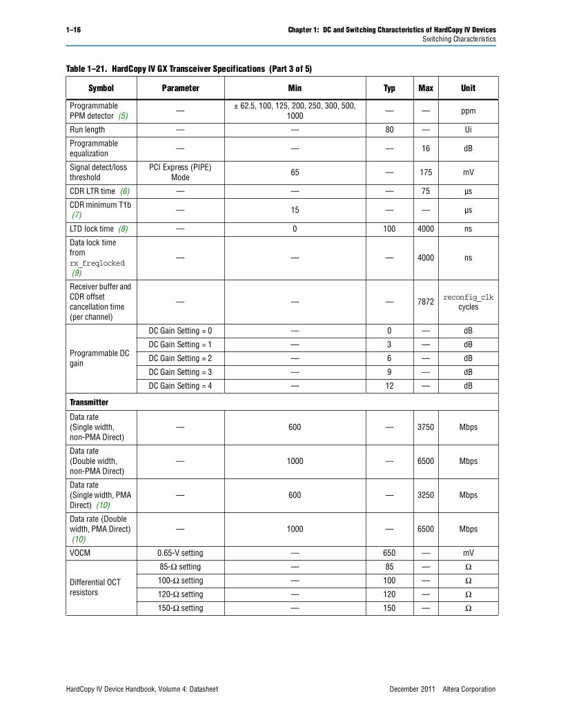
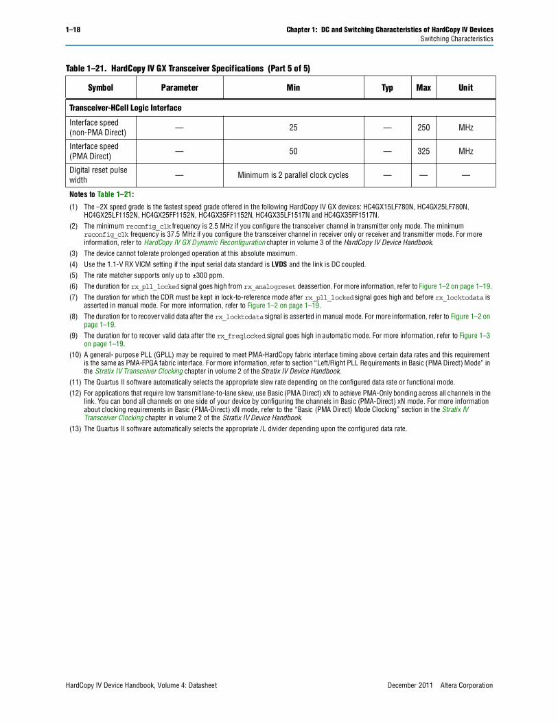
Transceiver Performance SpecificationsThis section describes transceiver performance specifications. Table 1–21 lists HardCopy IV GX transceiver specifications.
Table 1–21. HardCopy IV GX Transceiver Specifications (Part 1 of 5)
Symbol Parameter Min Typ Max Unit
Reference Clock
Input frequency from REFCLK input pins
— 50 — 672 MHz
Phase frequency detector (CMU PLL and receiver CDR)
— 50 — 325 MHz
Absolute Vmax for a REFCLK pin — — — 1.6 V
Operational Vmax for a REFCLK pin — — — 1.5 V
Absolute Vmin for a REFCLK pin — –0.4 — — V
Rise/fall time — — — 0.2 UI
Duty cycle — 45 — 55 %
Peak-to-peak differential input voltage
— 200 — 1600 mV
Spread-spectrum modulating clock frequency
PCI Express 30 — 33 kHz
Spread-spectrum downspread PCI Express — 0 to –0.5% — —
OCT resistors — — 100 — Ω
VICM (AC coupled) — — 1100 — mV
VICM (DC coupled)HCSL I/O standard for PCI Express reference
clock250 — 550 mV
Rref — — 2000 ±1% — Ω
Transceiver Clocks
Calibration block clock frequency — 10 — 125 MHz
fixedclk clock frequency
PCI Express Receiver Detect — 125 — MHz
reconfig_clk clock frequency
Dynamic reconfiguration clock frequency 2.5 or 37.5 (2) — 50 —
Transceiver block minimum power-down pulse width
— — 1 — µs

Chapter 1: DC and Switching Characteristics of HardCopy IV Devices 1–15Switching Characteristics
December 2011 Altera Corporation HardCopy IV Device Handbook, Volume 4: Datasheet
Receiver
Data rate (Single width, non-PMA Direct)
— 600 — 3750 Mbps
Data rate (Double width, non-PMA Direct)
— 1000 — 6500 Mbps
Data rate (Single width, PMA Direct)
— 600 — 3250 Mbps
Data rate (Double width, PMA Direct)
— 1000 — 6500 Mbps
Absolute Vmax for a receiver pin (3) — — — 1.6 V
Operational Vmax for a receiver pin — — — 1.5 V
Absolute Vmin for receiver pin — –0.4 — — V
Maximum peak-to-peak differential input voltage VID (diff p-p)
VICM = 0.82-V setting — — 2.7 V
VICM = 1.1-V setting (4) — — 1.6 V
Minimum peak-to-peak differential input voltage VID (diff p-p)
Data Rate = 600 Mbps to 5 Gbps 100 — — mV
Data Rate > 5 Gbps 165 — — mV
VICM VICM = 0.82-V setting — 820 — mV
VICM = 1.1-V setting (4) — 1100 — mV
Differential OCT resistors
85-Ω setting — 85 — Ω
100-Ω setting — 100 — Ω
120-Ω setting — 120 — Ω
150-Ω setting — 150 — Ω
Return loss differential mode
PCI Express 50 MHz to 1.25 GHz: –10dB — — —
XAUI 100 MHz to 2.5 GHz: –10dB — — —
(OIF) CEI100 MHz to 4.875 GHz: –8dB
4.875GHz to 10GHz: 16.6 dB/decade slope
— — —
Return loss common mode
PCI Express 50 MHz to 1.25 GHz: –6dB — — —
XAUI 100 MHz to 2.5 GHz: –6dB — — —
(OIF) CEI100 MHz to 4.875 GHz: –6dB
4.875GHz to 10GHz: 16.6 dB/decade slope
— — —
Table 1–21. HardCopy IV GX Transceiver Specifications (Part 2 of 5)
Symbol Parameter Min Typ Max Unit
1–16 Chapter 1: DC and Switching Characteristics of HardCopy IV DevicesSwitching Characteristics
HardCopy IV Device Handbook, Volume 4: Datasheet December 2011 Altera Corporation
Programmable PPM detector (5) — ± 62.5, 100, 125, 200, 250, 300, 500,
1000 — — ppm
Run length — — 80 — Ui
Programmable equalization — — — 16 dB
Signal detect/loss threshold
PCI Express (PIPE) Mode 65 — 175 mV
CDR LTR time (6) — — — 75 µs
CDR minimum T1b (7) — 15 — — µs
LTD lock time (8) — 0 100 4000 ns
Data lock time from rx_freqlocked (9)
— — — 4000 ns
Receiver buffer and CDR offset cancellation time (per channel)
— — — 7872 reconfig_clk cycles
Programmable DC gain
DC Gain Setting = 0 — 0 — dB
DC Gain Setting = 1 — 3 — dB
DC Gain Setting = 2 — 6 — dB
DC Gain Setting = 3 — 9 — dB
DC Gain Setting = 4 — 12 — dB
Transmitter
Data rate (Single width, non-PMA Direct)
— 600 — 3750 Mbps
Data rate (Double width, non-PMA Direct)
— 1000 — 6500 Mbps
Data rate (Single width, PMA Direct) (10)
— 600 — 3250 Mbps
Data rate (Double width, PMA Direct) (10)
— 1000 — 6500 Mbps
VOCM 0.65-V setting — 650 — mV
Differential OCT resistors
85-Ω setting — 85 — Ω
100-Ω setting — 100 — Ω
120-Ω setting — 120 — Ω
150-Ω setting — 150 — Ω
Table 1–21. HardCopy IV GX Transceiver Specifications (Part 3 of 5)
Symbol Parameter Min Typ Max Unit

Chapter 1: DC and Switching Characteristics of HardCopy IV Devices 1–17Switching Characteristics
December 2011 Altera Corporation HardCopy IV Device Handbook, Volume 4: Datasheet
Return loss differential mode
PCI Express 50 MHz to 1.25 GHz: –10 dB — — —
XAUI312 MHz to 625 MHz: –10 dB
625 MHz to 3.125 GHz: -10 dB/decade slope
— — —
(OIF) CEI100 MHz to 4.875 GHz: –8 dB
4.875 GHz to 10 GHz: 16.6 dB/decade slope
— — —
Return loss common mode
PCI Express 50 MHz to 1.25 GHz: –6 dB — — —
(OIF) CEI100 MHz to 4.875 GHz: –6 dB
4.875 GHz to 10 GHz: 16.6 dB/decade slope
— — —
Rise time — 50 — 200 ps
Fall time (11) — 50 — 200 ps
Intra differential pair skew — — — 15 ps
Intra-transceiver block skew ×4 PMA and PCS bonded
XAUI, PCI Express (PIPE) ×4, Basic ×4 — — 120 ps
Inter-transceiver block skew ×8 PMA and PCS bonded
PCI Express (PIPE) ×8, Basic ×8 — — 500 ps
Inter-transceiver block skew ×N PMA-Only bonded (12)
N < 18 channels located across three transceiver blocks with the source CMU PLL located in the center transceiver block
— — 400 ps
CMU PLL0 and CMU PLL1
Supported Data Range — 600 — 6500 Mbps
CMU PLL lock time from pll_powerdown deassertion
— — — 100 µs
ATX PLL
Supported Data Range (13)
/L = 1 4800 to 5400 and 6000 to 6375 — — Mbps
/L = 2 2400 to 2700 and 3000 to 3187.5 — — Mbps
/L = 4 1200 to 1350 and 1500 to 1593.75 — — Mbps
Table 1–21. HardCopy IV GX Transceiver Specifications (Part 4 of 5)
Symbol Parameter Min Typ Max Unit
1–18 Chapter 1: DC and Switching Characteristics of HardCopy IV DevicesSwitching Characteristics
HardCopy IV Device Handbook, Volume 4: Datasheet December 2011 Altera Corporation
Transceiver-HCell Logic Interface
Interface speed (non-PMA Direct) — 25 — 250 MHz
Interface speed (PMA Direct) — 50 — 325 MHz
Digital reset pulse width — Minimum is 2 parallel clock cycles — — —
Notes to Table 1–21:
(1) The –2X speed grade is the fastest speed grade offered in the following HardCopy IV GX devices: HC4GX15LF780N, HC4GX25LF780N, HC4GX25LF1152N, HC4GX25FF1152N, HC4GX35FF1152N, HC4GX35LF1517N and HC4GX35FF1517N.
(2) The minimum reconfig_clk frequency is 2.5 MHz if you configure the transceiver channel in transmitter only mode. The minimum reconfig_clk frequency is 37.5 MHz if you configure the transceiver channel in receiver only or receiver and transmitter mode. For more information, refer to HardCopy IV GX Dynamic Reconfiguration chapter in volume 3 of the HardCopy IV Device Handbook.
(3) The device cannot tolerate prolonged operation at this absolute maximum.(4) Use the 1.1-V RX VICM setting if the input serial data standard is LVDS and the link is DC coupled.(5) The rate matcher supports only up to ±300 ppm.(6) The duration for rx_pll_locked signal goes high from rx_analogreset deassertion. For more information, refer to Figure 1–2 on page 1–19.(7) The duration for which the CDR must be kept in lock-to-reference mode after rx_pll_locked signal goes high and before rx_locktodata is
asserted in manual mode. For more information, refer to Figure 1–2 on page 1–19.(8) The duration for to recover valid data after the rx_locktodata signal is asserted in manual mode. For more information, refer to Figure 1–2 on
page 1–19.(9) The duration for to recover valid data after the rx_freqlocked signal goes high in automatic mode. For more information, refer to Figure 1–3
on page 1–19.(10) A general- purpose PLL (GPLL) may be required to meet PMA-HardCopy fabric interface timing above certain data rates and this requirement
is the same as PMA-FPGA fabric interface. For more information, refer to section “Left/Right PLL Requirements in Basic (PMA Direct) Mode” in the Stratix IV Transceiver Clocking chapter in volume 2 of the Stratix IV Device Handbook.
(11) The Quartus II software automatically selects the appropriate slew rate depending on the configured data rate or functional mode.(12) For applications that require low transmit lane-to-lane skew, use Basic (PMA Direct) xN to achieve PMA-Only bonding across all channels in the
link. You can bond all channels on one side of your device by configuring the channels in Basic (PMA-Direct) xN mode. For more information about clocking requirements in Basic (PMA-Direct) xN mode, refer to the “Basic (PMA Direct) Mode Clocking” section in the Stratix IV Transceiver Clocking chapter in volume 2 of the Stratix IV Device Handbook.
(13) The Quartus II software automatically selects the appropriate /L divider depending upon the configured data rate.
Table 1–21. HardCopy IV GX Transceiver Specifications (Part 5 of 5)
Symbol Parameter Min Typ Max Unit
Chapter 1: DC and Switching Characteristics of HardCopy IV Devices 1–19Switching Characteristics
December 2011 Altera Corporation HardCopy IV Device Handbook, Volume 4: Datasheet
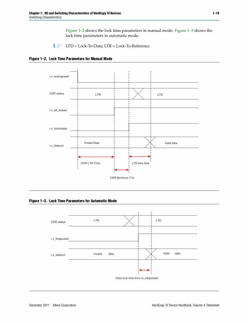
Figure 1–2 shows the lock time parameters in manual mode. Figure 1–3 shows the lock time parameters in automatic mode.
1 LTD = Lock-To-Data; LTR = Lock-To-Reference
Figure 1–2. Lock Time Parameters for Manual Mode
Figure 1–3. Lock Time Parameters for Automatic Mode
LTR LTD
Invalid Data Valid data
r x_locktodata
LTD lock time
CDR status
r x_dataout
r x_pll_locked
r x_analogreset
CDR LTR Time
CDR Minimum T1b
LTR LTD
Invalid data Valid data
r x_freqlocked
Data lock time from rx_freqlocked
r x_dataout
CDR status
1–20 Chapter 1: DC and Switching Characteristics of HardCopy IV DevicesSwitching Characteristics
HardCopy IV Device Handbook, Volume 4: Datasheet December 2011 Altera Corporation
Table 1–22 through Table 1–25 list the typical VOD for various differential termination settings for HardCopy IV GX devices.
Table 1–26 lists typical transmitter pre-emphasis levels in dB for the first post tap under the following conditions (low-frequency data pattern [five 1s and five 0s] at 6.25 Gbps). The levels listed in Table 1–26 are a representation of possible pre-emphasis levels under the specified conditions only and that the pre-emphasis levels may change with data pattern and data rate.
1 To estimate the pre-emphasis level for your specific data rate and pattern, run simulations using the HardCopy IV high-speed serial interface (HSSI) HSPICE models.
Table 1–22. Typical VOD Setting, TX Term = 85 Ω
SymbolVOD Setting (mV)
0 1 2 3 4 5 6 7
VOD differential peak-to-peak Typical (mV)
170±20%
340±20%
510±20%
595±20%
680±20%
765±20%
850±20%
1020±20%
Table 1–23. Typical VOD Setting, TX Term = 100 Ω
SymbolVOD Setting (mV)
0 1 2 3 4 5 6 7
VOD differential peak-to-peak Typical (mV)
200±20%
400±20%
600±20%
700±20%
800±20%
900±20%
1000±20%
1200±20%
Table 1–24. Typical VOD Setting, TX Term = 120 Ω
SymbolVOD Setting (mV)
0 1 2 3 4 5 6 7
VOD differential peak-to-peak Typical (mV)
240± 20%
480± 20%
600± 20%
720± 20%
840± 20%
960± 20%
1080± 20%
1200± 20%
Table 1–25. Typical VOD Setting, TX Term = 150 Ω
SymbolVOD Setting (mV)
0 1 2 3 4 5
VOD differential peak-to-peak Typical (mV)
300± 20%
600± 20%
900± 20%
1050± 20%
1200± 20%
1350± 20%

Chapter 1: DC and Switching Characteristics of HardCopy IV Devices 1–21Switching Characteristics
December 2011 Altera Corporation HardCopy IV Device Handbook, Volume 4: Datasheet
Table 1–26. Transmitter Pre-emphasis Levels for HardCopy IV Devices
Pre-emphasis
First Post-Tap Setting
VOD Setting
0 1 2 3 4 5 6 7
0 0 0 0 0 0 0 0 0
1 — 0.7 0 0 0 0 0 0
2 — 1 0.3 0 0 0 0 0
3 — 1.5 0.6 0 0 0 0 0
4 — 2 0.7 0.3 0 0 0 0
5 — 2.7 1.2 0.5 0.3 0 0 0
6 — 3.1 1.3 0.8 0.5 0.2 0 0
7 — 3.7 1.8 1.1 0.7 0.4 0.2 0
8 — 4.2 2.1 1.3 0.9 0.6 0.3 0
9 — 4.9 2.4 1.6 1.2 0.8 0.5 0.2
10 — 5.4 2.8 1.9 1.4 1 0.7 0.3
11 — 6 3.2 2.2 1.7 1.2 0.9 0.4
12 — 6.8 3.5 2.6 1.9 1.4 1.1 0.6
13 — 7.5 3.8 2.8 2.1 1.6 1.2 0.6
14 — 8.1 4.2 3.1 2.3 1.7 1.3 0.7
15 — 8.8 4.5 3.4 2.6 1.9 1.5 0.8
16 — — 4.9 3.7 2.9 2.2 1.7 0.9
17 — — 5.3 4 3.1 2.4 1.8 1.1
18 — — 5.7 4.4 3.4 2.6 2 1.2
19 — — 6.1 4.7 3.6 2.8 2.2 1.4
20 — — 6.6 5.1 4 3.1 2.4 1.5
21 — — 7 5.4 4.3 3.3 2.7 1.7
22 — — 8 6.1 4.8 3.8 3 2
23 — — 9 6.8 5.4 4.3 3.4 2.3
24 — — 10 7.6 6 4.8 3.9 2.6
25 — — 11.4 8.4 6.8 5.4 4.4 3
26 — — 12.6 9.4 7.4 5.9 4.9 3.3
27 — — — 10.3 8.1 6.4 5.3 3.6
28 — — — 11.3 8.8 7.1 5.8 4
29 — — — 12.5 9.6 7.7 6.3 4.3
30 — — — — 11.4 9 7.4 —
31 — — — — 12.9 10 8.2 —
1–22 Chapter 1: DC and Switching Characteristics of HardCopy IV DevicesSwitching Characteristics
HardCopy IV Device Handbook, Volume 4: Datasheet December 2011 Altera Corporation
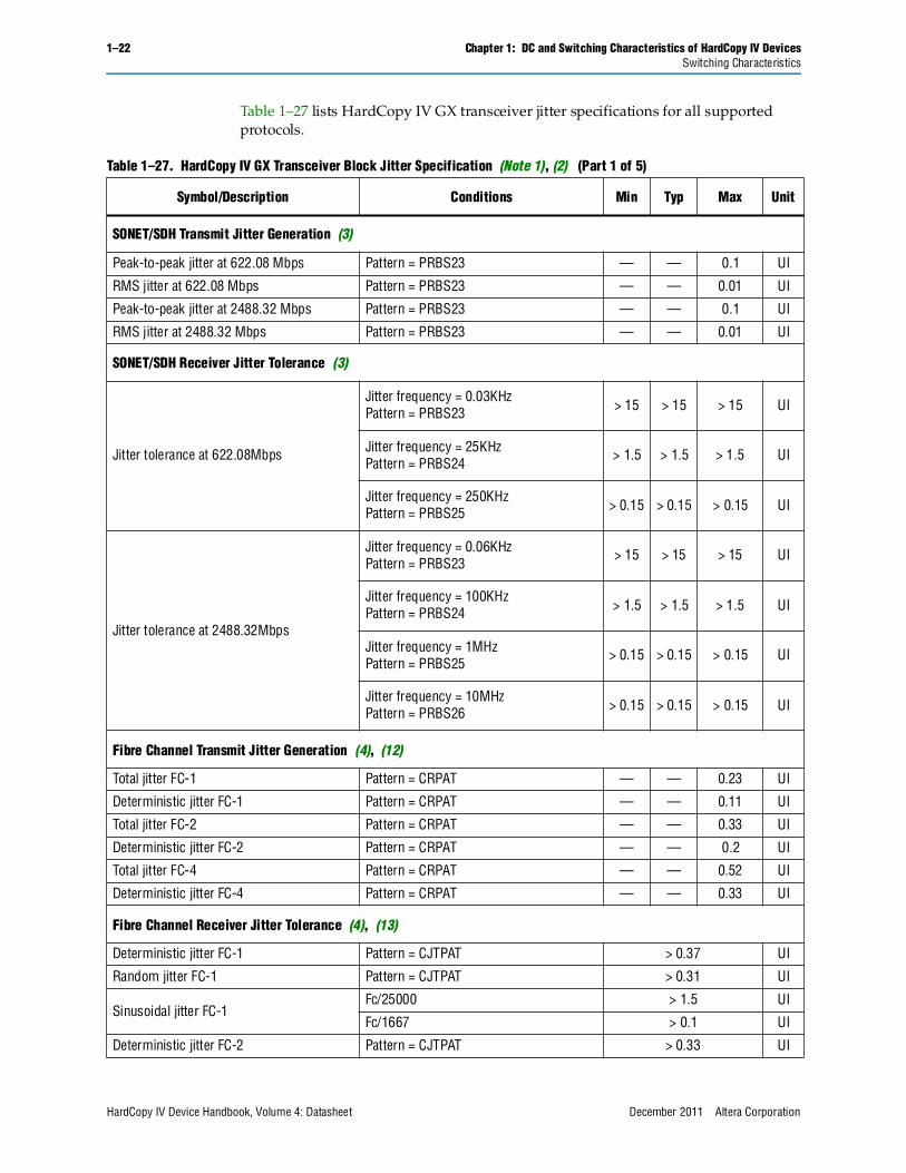
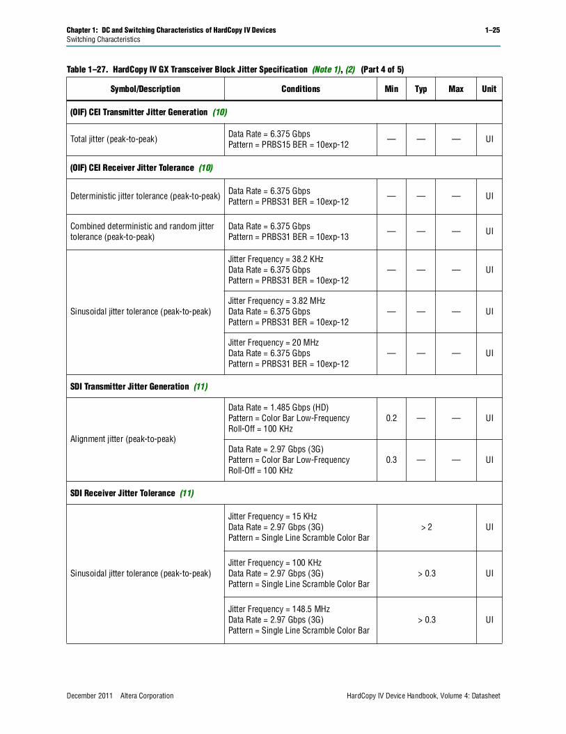
Table 1–27 lists HardCopy IV GX transceiver jitter specifications for all supported protocols.
Table 1–27. HardCopy IV GX Transceiver Block Jitter Specification (Note 1), (2) (Part 1 of 5)
Symbol/Description Conditions Min Typ Max Unit
SONET/SDH Transmit Jitter Generation (3)
Peak-to-peak jitter at 622.08 Mbps Pattern = PRBS23 — — 0.1 UI
RMS jitter at 622.08 Mbps Pattern = PRBS23 — — 0.01 UI
Peak-to-peak jitter at 2488.32 Mbps Pattern = PRBS23 — — 0.1 UI
RMS jitter at 2488.32 Mbps Pattern = PRBS23 — — 0.01 UI
SONET/SDH Receiver Jitter Tolerance (3)
Jitter tolerance at 622.08Mbps
Jitter frequency = 0.03KHzPattern = PRBS23 > 15 > 15 > 15 UI
Jitter frequency = 25KHzPattern = PRBS24
> 1.5 > 1.5 > 1.5 UI
Jitter frequency = 250KHzPattern = PRBS25 > 0.15 > 0.15 > 0.15 UI
Jitter tolerance at 2488.32Mbps
Jitter frequency = 0.06KHzPattern = PRBS23
> 15 > 15 > 15 UI
Jitter frequency = 100KHzPattern = PRBS24 > 1.5 > 1.5 > 1.5 UI
Jitter frequency = 1MHzPattern = PRBS25
> 0.15 > 0.15 > 0.15 UI
Jitter frequency = 10MHzPattern = PRBS26 > 0.15 > 0.15 > 0.15 UI
Fibre Channel Transmit Jitter Generation (4), (12)
Total jitter FC-1 Pattern = CRPAT — — 0.23 UI
Deterministic jitter FC-1 Pattern = CRPAT — — 0.11 UI
Total jitter FC-2 Pattern = CRPAT — — 0.33 UI
Deterministic jitter FC-2 Pattern = CRPAT — — 0.2 UI
Total jitter FC-4 Pattern = CRPAT — — 0.52 UI
Deterministic jitter FC-4 Pattern = CRPAT — — 0.33 UI
Fibre Channel Receiver Jitter Tolerance (4), (13)
Deterministic jitter FC-1 Pattern = CJTPAT > 0.37 UI
Random jitter FC-1 Pattern = CJTPAT > 0.31 UI
Sinusoidal jitter FC-1Fc/25000 > 1.5 UI
Fc/1667 > 0.1 UI
Deterministic jitter FC-2 Pattern = CJTPAT > 0.33 UI

Chapter 1: DC and Switching Characteristics of HardCopy IV Devices 1–23Switching Characteristics
December 2011 Altera Corporation HardCopy IV Device Handbook, Volume 4: Datasheet
Random jitter FC-2 Pattern = CJTPAT > 0.29 UI
Sinusoidal jitter FC-2Fc/25000 > 1.5 UI
Fc/1667 > 0.1 UI
Deterministic jitter FC-4 Pattern = CJTPAT > 0.33 UI
Random jitter FC-4 Pattern = CJTPAT > 0.29 UI
Sinusoidal jitter FC-4Fc/25000 > 1.5 UI
Fc/1667 > 0.1 UI
XAUI Transmit Jitter Generation (5)
Total jitter at 3.125 Gbps Pattern = CJPAT — — 0.3 UI
Deterministic jitter at 3.125 Gbps Pattern = CJPAT — — 0.17 UI
XAUI Receiver Jitter Tolerance (5)
Total jitter — > 0.65 UI
Deterministic jitter — > 0.37 UI
Peak-to-peak jitter Jitter frequency = 22.1 KHz > 8.5 UI
Peak-to-peak jitter Jitter frequency = 1.875 MHz > 0.1 UI
Peak-to-peak jitter Jitter frequency = 20 MHz > 0.1 UI
PCI Express Transmit Jitter Generation (6)
Total jitter at 2.5 Gbps (Gen1) Compliance pattern — — 0.25 UI
Total jitter at 5 Gbps (Gen2) Compliance pattern — — — UI
PCI Express Receiver Jitter Tolerance (6)
Total jitter at 2.5 Gbps (Gen1) Compliance pattern > 0.6 UI
Total jitter at 2.5 Gbps (Gen2) Compliance pattern — — — UI
Serial RapidIO Transmit Jitter Generation (7)
Deterministic jitter (peak-to-peak)Data Rate = 1.25, 2.5, 3.125 GbpsPattern = CJPAT — — 0.17 UI
Total jitter (peak-to-peak) Data Rate = 1.25, 2.5, 3.125 GbpsPattern = CJPAT
— — 0.35 UI
Serial RapidIO Receiver Jitter Tolerance (7)
Deterministic jitter (peak-to-peak)Data Rate = 1.25, 2.5, 3.125 GbpsPattern = CJPAT > 0.37 UI
Combined deterministic and random jitter tolerance (peak-to-peak)
Data Rate = 1.25, 2.5, 3.125 GbpsPattern = CJPAT
> 0.55 UI
Table 1–27. HardCopy IV GX Transceiver Block Jitter Specification (Note 1), (2) (Part 2 of 5)
Symbol/Description Conditions Min Typ Max Unit

1–24 Chapter 1: DC and Switching Characteristics of HardCopy IV DevicesSwitching Characteristics
HardCopy IV Device Handbook, Volume 4: Datasheet December 2011 Altera Corporation
Sinusoidal jitter tolerance (peak-to-peak)
Jitter Frequency = 22.1 KHzData Rate = 1.25, 2.5, 3.125 GbpsPattern = CJPAT
> 8.5 UI
Jitter Frequency = 1.875 MHzData Rate = 1.25, 2.5, 3.125 GbpsPattern = CJPAT
> 0.1 UI
Jitter Frequency = 20 MHzData Rate = 1.25, 2.5, 3.125 GbpsPattern = CJPAT
> 0.1 UI
GIGE Transmit Jitter Generation (8)
Deterministic jitter (peak-to-peak) Pattern = CRPAT — — 0.14 UI
Total jitter (peak-to-peak) Pattern = CRPAT — — 0.279 UI
GIGE Receiver Jitter Tolerance (8)
Deterministic jitter (peak-to-peak) Pattern = CJPAT > 0.4 UI
Combined deterministic and random jitter tolerance (peak-to-peak)
Pattern = CJPAT > 0.66 UI
HiGig Transmit Jitter Generation (9)
Deterministic jitter (peak-to-peak)Data Rate = 3.75 GbpsPattern = CJPAT — — — UI
Total jitter (peak-to-peak) Data Rate = 3.75 GbpsPattern = CJPAT
— — — UI
HiGig Receiver Jitter Tolerance (9)
Deterministic jitter tolerance (peak-to-peak)Data Rate = 3.75 GbpsPattern = CJPAT — — — UI
Combined deterministic and random jitter tolerance (peak-to-peak)
Data Rate = 3.75 GbpsPattern = CJPAT
— — — UI
Sinusoidal jitter tolerance (peak-to-peak)
Jitter Frequency = 22.1 KHzData Rate = 3.75 GbpsPattern = CJPAT
— — — UI
Jitter Frequency = 1.875 MHzData Rate = 3.75 GbpsPattern = CJPAT
— — — UI
Jitter Frequency = 20 MHzData Rate = 3.75 GbpsPattern = CJPAT
— — — UI
Table 1–27. HardCopy IV GX Transceiver Block Jitter Specification (Note 1), (2) (Part 3 of 5)
Symbol/Description Conditions Min Typ Max Unit
Chapter 1: DC and Switching Characteristics of HardCopy IV Devices 1–25Switching Characteristics
December 2011 Altera Corporation HardCopy IV Device Handbook, Volume 4: Datasheet
(OIF) CEI Transmitter Jitter Generation (10)
Total jitter (peak-to-peak) Data Rate = 6.375 GbpsPattern = PRBS15 BER = 10exp-12
— — — UI
(OIF) CEI Receiver Jitter Tolerance (10)
Deterministic jitter tolerance (peak-to-peak) Data Rate = 6.375 GbpsPattern = PRBS31 BER = 10exp-12
— — — UI
Combined deterministic and random jitter tolerance (peak-to-peak)
Data Rate = 6.375 GbpsPattern = PRBS31 BER = 10exp-13
— — — UI
Sinusoidal jitter tolerance (peak-to-peak)
Jitter Frequency = 38.2 KHzData Rate = 6.375 GbpsPattern = PRBS31 BER = 10exp-12
— — — UI
Jitter Frequency = 3.82 MHzData Rate = 6.375 GbpsPattern = PRBS31 BER = 10exp-12
— — — UI
Jitter Frequency = 20 MHzData Rate = 6.375 GbpsPattern = PRBS31 BER = 10exp-12
— — — UI
SDI Transmitter Jitter Generation (11)
Alignment jitter (peak-to-peak)
Data Rate = 1.485 Gbps (HD)Pattern = Color Bar Low-Frequency Roll-Off = 100 KHz
0.2 — — UI
Data Rate = 2.97 Gbps (3G)Pattern = Color Bar Low-Frequency Roll-Off = 100 KHz
0.3 — — UI
SDI Receiver Jitter Tolerance (11)
Sinusoidal jitter tolerance (peak-to-peak)
Jitter Frequency = 15 KHzData Rate = 2.97 Gbps (3G)Pattern = Single Line Scramble Color Bar
> 2 UI
Jitter Frequency = 100 KHzData Rate = 2.97 Gbps (3G)Pattern = Single Line Scramble Color Bar
> 0.3 UI
Jitter Frequency = 148.5 MHzData Rate = 2.97 Gbps (3G)Pattern = Single Line Scramble Color Bar
> 0.3 UI
Table 1–27. HardCopy IV GX Transceiver Block Jitter Specification (Note 1), (2) (Part 4 of 5)
Symbol/Description Conditions Min Typ Max Unit
1–26 Chapter 1: DC and Switching Characteristics of HardCopy IV DevicesSwitching Characteristics
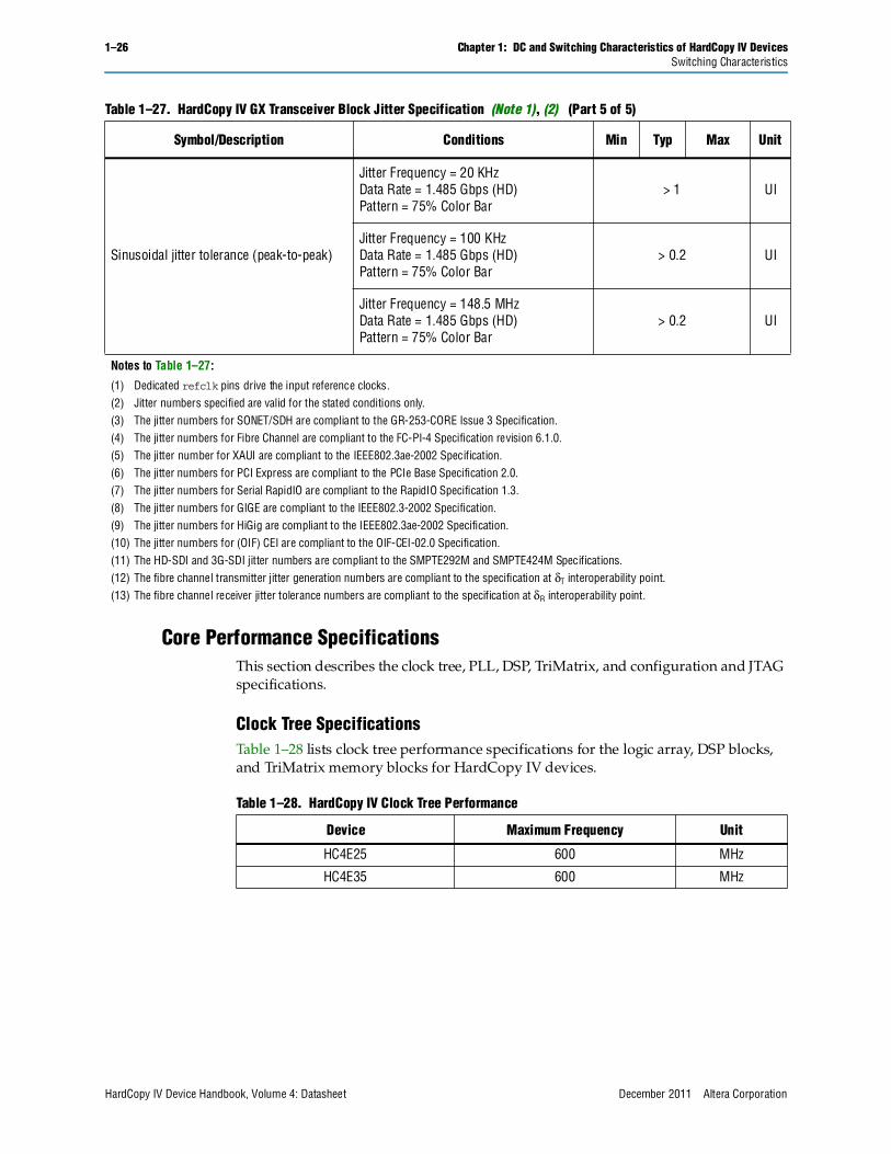
HardCopy IV Device Handbook, Volume 4: Datasheet December 2011 Altera Corporation
Core Performance SpecificationsThis section describes the clock tree, PLL, DSP, TriMatrix, and configuration and JTAG specifications.
Clock Tree SpecificationsTable 1–28 lists clock tree performance specifications for the logic array, DSP blocks, and TriMatrix memory blocks for HardCopy IV devices.
Sinusoidal jitter tolerance (peak-to-peak)
Jitter Frequency = 20 KHzData Rate = 1.485 Gbps (HD)Pattern = 75% Color Bar
> 1 UI
Jitter Frequency = 100 KHzData Rate = 1.485 Gbps (HD)Pattern = 75% Color Bar
> 0.2 UI
Jitter Frequency = 148.5 MHzData Rate = 1.485 Gbps (HD)Pattern = 75% Color Bar
> 0.2 UI
Notes to Table 1–27:
(1) Dedicated refclk pins drive the input reference clocks.(2) Jitter numbers specified are valid for the stated conditions only.(3) The jitter numbers for SONET/SDH are compliant to the GR-253-CORE Issue 3 Specification.(4) The jitter numbers for Fibre Channel are compliant to the FC-PI-4 Specification revision 6.1.0.(5) The jitter number for XAUI are compliant to the IEEE802.3ae-2002 Specification.(6) The jitter numbers for PCI Express are compliant to the PCIe Base Specification 2.0.(7) The jitter numbers for Serial RapidIO are compliant to the RapidIO Specification 1.3.(8) The jitter numbers for GIGE are compliant to the IEEE802.3-2002 Specification.(9) The jitter numbers for HiGig are compliant to the IEEE802.3ae-2002 Specification.(10) The jitter numbers for (OIF) CEI are compliant to the OIF-CEI-02.0 Specification.(11) The HD-SDI and 3G-SDI jitter numbers are compliant to the SMPTE292M and SMPTE424M Specifications.(12) The fibre channel transmitter jitter generation numbers are compliant to the specification at δT interoperability point.(13) The fibre channel receiver jitter tolerance numbers are compliant to the specification at δR interoperability point.
Table 1–27. HardCopy IV GX Transceiver Block Jitter Specification (Note 1), (2) (Part 5 of 5)
Symbol/Description Conditions Min Typ Max Unit
Table 1–28. HardCopy IV Clock Tree Performance
Device Maximum Frequency Unit
HC4E25 600 MHz
HC4E35 600 MHz
Chapter 1: DC and Switching Characteristics of HardCopy IV Devices 1–27Switching Characteristics
December 2011 Altera Corporation HardCopy IV Device Handbook, Volume 4: Datasheet
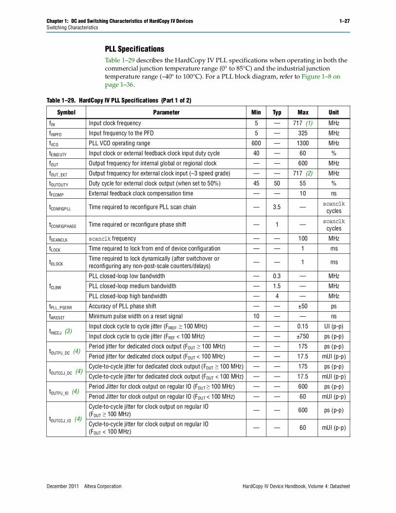
PLL SpecificationsTable 1–29 describes the HardCopy IV PLL specifications when operating in both the commercial junction temperature range (0° to 85°C) and the industrial junction temperature range (–40° to 100°C). For a PLL block diagram, refer to Figure 1–8 on page 1–36.
Table 1–29. HardCopy IV PLL Specifications (Part 1 of 2)
Symbol Parameter Min Typ Max Unit
fIN Input clock frequency 5 — 717 (1) MHz
fINPFD Input frequency to the PFD 5 — 325 MHz
fVCO PLL VCO operating range 600 — 1300 MHz
tEINDUTY Input clock or external feedback clock input duty cycle 40 — 60 %
fOUT Output frequency for internal global or regional clock — — 600 MHz
fOUT_EXT Output frequency for external clock input (–3 speed grade) — — 717 (2) MHz
tOUTDUTY Duty cycle for external clock output (when set to 50%) 45 50 55 %
tFCOMP External feedback clock compensation time — — 10 ns
tCONFIGPLL Time required to reconfigure PLL scan chain — 3.5 — scanclk cycles
tCONFIGPHASE Time required or reconfigure phase shift — 1 — scanclk cycles
fSCANCLK scanclk frequency — — 100 MHz
tLOCK Time required to lock from end of device configuration — — 1 ms
tDLOCKTime required to lock dynamically (after switchover or reconfiguring any non-post-scale counters/delays)
— — 1 ms
fCLBW
PLL closed-loop low bandwidth — 0.3 — MHz
PLL closed-loop medium bandwidth — 1.5 — MHz
PLL closed-loop high bandwidth — 4 — MHz
tPLL_PSERR Accuracy of PLL phase shift — — ±50 ps
tARESET Minimum pulse width on a reset signal 10 — — ns
tINCCJ (3)Input clock cycle to cycle jitter (FREF ≥ 100 MHz) — — 0.15 UI (p-p)
Input clock cycle to cycle jitter (FREF < 100 MHz) — — ±750 ps (p-p)
tOUTPJ_DC (4)Period jitter for dedicated clock output (FOUT ≥ 100 MHz) — — 175 ps (p-p)
Period jitter for dedicated clock output (FOUT < 100 MHz) — — 17.5 mUI (p-p)
tOUTCCJ_DC (4)Cycle-to-cycle jitter for dedicated clock output (FOUT ≥ 100 MHz) — — 175 ps (p-p)
Cycle-to-cycle jitter for dedicated clock output (FOUT < 100 MHz) — — 17.5 mUI (p-p)
tOUTPJ_IO (4)Period Jitter for clock output on regular IO (FOUT ≥ 100 MHz) — — 600 ps (p-p)
Period Jitter for clock output on regular IO (FOUT < 100 MHz) — — 60 mUI (p-p)
tOUTCCJ_IO (4)
Cycle-to-cycle jitter for clock output on regular IO (FOUT ≥ 100 MHz)
— — 600 ps (p-p)
Cycle-to-cycle jitter for clock output on regular IO (FOUT < 100 MHz)
— — 60 mUI (p-p)

1–28 Chapter 1: DC and Switching Characteristics of HardCopy IV DevicesSwitching Characteristics
HardCopy IV Device Handbook, Volume 4: Datasheet December 2011 Altera Corporation
DSP Block Specifications Table 1–30 describes the HardCopy IV DSP block performance specifications.
tCASC_OUTPJ_DC (4)
Period Jitter for dedicated clock output in cascaded PLLs (FOUT ≥ 100 MHz)
— — 250 ps (p-p)
Period Jitter for dedicated clock output in cascaded PLLs (FOUT < 100 MHz)
— — 25 mUI (p-p)
fDRIFT Frequency drift after PFDENA is disabled for duration of 100 us — — ±10 %
Notes to Table 1–29:
(1) This specification is limited in Quartus II software by the I/O maximum frequency. The maximum I/O frequency is different for each I/O standard. (2) This specification is limited by the lower of the two: I/O FMAX or FOUT of the PLL.(3) A high input jitter directly affects the PLL output jitter. To have low PLL output clock jitter, you must provide a clean clock source, which is less
than 120 ps.(4) Peak-to-peak jitter with a probability level of 10–12 (14 sigma, 99.99999999974404% confidence level). The output jitter specification applies
to the intrinsic jitter of the PLL, when an input jitter of 30 ps is applied. The external memory interface clock output jitter specifications use a different measurement method and are available in Table 1–38.
Table 1–29. HardCopy IV PLL Specifications (Part 2 of 2)
Symbol Parameter Min Typ Max Unit
Table 1–30. HardCopy IV DSP Block Performance Specifications (Note 1)
Mode Number of Multipliers
Maximum FrequencyUnit
Flipchip Wirebond
9 × 9-bit multiplier (a, c, e, g) 1 345 276 MHz
9 × 9-bit multiplier (b, d, f, h) 1 385 308 MHz
12 × 12-bit multiplier (a, e) 1 345 276 MHz
12 × 12-bit multiplier (b, d, f, h) 1 385 308 MHz
18 × 18-bit multiplier 1 425 340 MHz
36 × 36-bit multiplier 1 345 276 MHz
18 × 18-bit multiply accumulator 4 370 296 MHz
18 × 18-bit multiply adder 4 380 304 MHz
18 × 18-bit multiply adder-signed full precision 2 380 304 MHz
18 × 18-bit multiply adder with loopback (2) 2 300 240 MHz
36-bit shift (32 bit data) 1 370 296 MHz
Double mode 1 345 276 MHz
Notes to Table 1–30:
(1) Maximum is for fully pipelined block with Round and Saturation disabled.(2) Maximum is for non-pipelined block with loopback input registers disabled and Round and Saturation disabled.
Chapter 1: DC and Switching Characteristics of HardCopy IV Devices 1–29Switching Characteristics
December 2011 Altera Corporation HardCopy IV Device Handbook, Volume 4: Datasheet
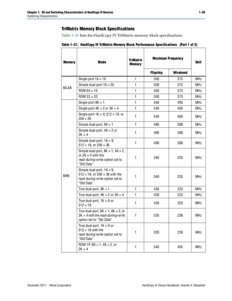
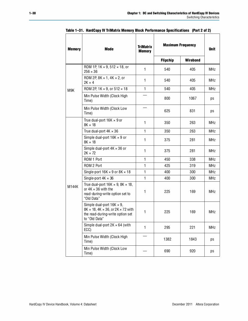
TriMatrix Memory Block SpecificationsTable 1–31 lists the HardCopy IV TriMatrix memory block specifications.
Table 1–31. HardCopy IV TriMatrix Memory Block Performance Specifications (Part 1 of 2)
Memory Mode TriMatrix Memory
Maximum FrequencyUnit
Flipchip Wirebond
MLAB
Single port 16 × 10 1 500 375 MHz
Simple dual-port 16 × 20 1 500 375 MHz
ROM 64 × 10 1 500 375 MHz
ROM 32 × 20 1 500 375 MHz
M9K
Single-port 8K × 1 1 540 405 MHz
Single-port 4K × 2 or 2K × 4 1 540 405 MHz
Single-port 1K × 9, 512 × 18, or 256 × 36 1 540 405 MHz
Simple dual-port, 8K × 1 1 490 368 MHz
Simple dual-port, 4K × 2 or 2K × 4 1 490 368 MHz
Simple dual-port, 1K × 9, 512 × 18, or 256 × 36 1 490 368 MHz
Simple dual-port, 8K × 1, 4K × 2, or 2K × 4 with the read-during-write option set to “Old Data”
1 340 255 MHz
Simple dual-port, 1K × 9, 512 × 18, or 256 × 36 with the read-during-write option set to “Old Data”
1 340 255 MHz
True dual-port, 8K × 1 1 430 323 MHz
True dual-port, 4K × 2 or 2K × 4 1 430 323 MHz
True dual-port, 1K × 9 or 512 × 18 1 430 323 MHz
True dual-port, 8K × 1, 4K × 2, or 2K × 4 with the read-during-write option set to “Old Data”
1 335 236 MHz
True dual-port, 1K × 9 or 512 × 18 with the read-during-write option set to “Old Data”
1 335 236 MHz
ROM 1P, 8K × 1, 4K × 2, or 2K × 4 1 540 405 MHz
1–30 Chapter 1: DC and Switching Characteristics of HardCopy IV DevicesSwitching Characteristics
HardCopy IV Device Handbook, Volume 4: Datasheet December 2011 Altera Corporation
M9K
ROM 1P, 1K × 9, 512 × 18, or 256 × 36 1 540 405 MHz
ROM 2P, 8K × 1, 4K × 2, or 2K × 4 1 540 405 MHz
ROM 2P, 1K × 9, or 512 × 18 1 540 405 MHz
Min Pulse Width (Clock High Time)
—800 1067 ps
Min Pulse Width (Clock Low Time)
—625 831 ps
M144K
True dual-port 16K × 9 or 8K × 18 1 350 263 MHz
True dual-port 4K × 36 1 350 263 MHz
Simple dual-port 16K × 9 or 8K × 18 1 375 281 MHz
Simple dual-port 4K × 36 or 2K × 72 1 375 281 MHz
ROM 1 Port 1 450 338 MHz
ROM 2 Port 1 425 319 MHz
Single-port 16K × 9 or 8K × 18 1 400 300 MHz
Single-port 4K × 36 1 400 300 MHz
True dual-port 16K × 9, 8K × 18, or 4K × 36 with the read-during-write option set to “Old Data”
1 225 169 MHz
Simple dual-port 16K × 9, 8K × 18, 4K × 36, or 2K × 72 with the read-during-write option set to “Old Data”
1 225 169 MHz
Simple dual-port 2K × 64 (with ECC) 1 295 221 MHz
Min Pulse Width (Clock High Time)
—1382 1843 ps
Min Pulse Width (Clock Low Time) — 690 920 ps
Table 1–31. HardCopy IV TriMatrix Memory Block Performance Specifications (Part 2 of 2)
Memory Mode TriMatrix Memory
Maximum FrequencyUnit
Flipchip Wirebond
Chapter 1: DC and Switching Characteristics of HardCopy IV Devices 1–31Switching Characteristics
December 2011 Altera Corporation HardCopy IV Device Handbook, Volume 4: Datasheet
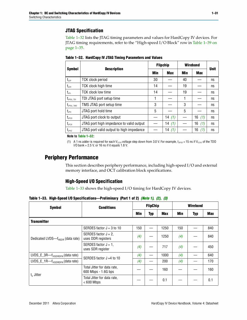
JTAG SpecificationTable 1–32 lists the JTAG timing parameters and values for HardCopy IV devices. For JTAG timing requirements, refer to the “High-speed I/O Block” row in Table 1–39 on page 1–35.
Periphery PerformanceThis section describes periphery performance, including high-speed I/O and external memory interface, and OCT calibration block specifications.
High-Speed I/O SpecificationTable 1–33 shows the high-speed I/O timing for HardCopy IV devices.
Table 1–32. HardCopy IV JTAG Timing Parameters and Values
Symbol DescriptionFlipchip Wirebond
UnitMin Max Min Max
tJCP TCK clock period 30 — 40 — ns
tJCH TCK clock high time 14 — 19 — ns
tJCL TCK clock low time 14 — 19 — ns
tJPSU_TDI TDI JTAG port setup time 1 — 1 — ns
tJPSU_TMS TMS JTAG port setup time 3 — 3 — ns
tJPH JTAG port hold time 5 — 5 — ns
tJPCO JTAG port clock to output — 14 (1) — 16 (1) ns
tJPZX JTAG port high impedance to valid output — 14 (1) — 16 (1) ns
tJPXZ JTAG port valid output to high impedance — 14 (1) — 16 (1) ns
Note to Table 1–32:
(1) A 1 ns adder is required for each VCCIO voltage step down from 3.0 V. For example, tJPCO = 15 ns if VCCIO of the TDO I/O bank = 2.5 V, or 16 ns if it equals 1.8 V.
Table 1–33. High-Speed I/O Specifications—Preliminary (Part 1 of 2) (Note 1), (2), (3)
Symbol Conditions FlipChip Wirebond
Min Typ Max Min Typ Max
Transmitter
Dedicated LVDS—fHSDR (data rate)
SERDES factor J = 3 to 10 150 — 1250 150 — 840
SERDES factor J = 2, uses DDR registers (4) — 1250 (4) — 840
SERDES factor J = 1, uses SDR register (4) — 717 (4) — 450
LVDS_E_3R—fHSDRDPA (data rate)SERDES factor J =4 to 10
(4) — 1000 (4) — 640
LVDS_E_1R—fHSDRDPA (data rate) (4) — 200 (4) — 170
tx Jitter
Total Jitter for data rate, 600 Mbps - 1.6G bps — — 160 — — 160
Total Jitter for data rate, < 600 Mbps — — 0.1 — — 0.1

1–32 Chapter 1: DC and Switching Characteristics of HardCopy IV DevicesSwitching Characteristics
HardCopy IV Device Handbook, Volume 4: Datasheet December 2011 Altera Corporation
tDUTY Tx output clock duty cycle 45 50 55 45 50 55
tRISE and tFALL
Dedicated LVDS — — 200 — 200 —
LVDS_E_3R — — 350 — 350 —
LVDS_E_1R — — 500 — 500 —
TCCSDedicated LVDS — — 100 — — 200
LVDS_E_3R/ LVDS_E_1R — — 250 — — 250
Receiver
fHSDRDPA (data rate) SERDES factor J = 3 to 10 150 — 1250 150 — 840
DPA Mode
DPA run length — — — 10000 — — 10000
Soft CDR mode
Soft-CDR PPM tolerance — — — 300 — —
Non DPA Mode
Sampling Window All differential I/O standards — — 300 — — 400
Notes to Table 1–33:
(1) Numbers are preliminary pending characterization. (2) When J = 3 to 10, the SERDES block is used.(3) When J = 1 or 2, the SERDES block is bypassed.(4) The minimum specification is dependent on the clock source (for example, PLL and clock pin) and the clock routing resource (global, regional,
or local) is used.
Table 1–33. High-Speed I/O Specifications—Preliminary (Part 2 of 2) (Note 1), (2), (3)
Symbol Conditions FlipChip Wirebond
Min Typ Max Min Typ Max

Chapter 1: DC and Switching Characteristics of HardCopy IV Devices 1–33Switching Characteristics
December 2011 Altera Corporation HardCopy IV Device Handbook, Volume 4: Datasheet
Table 1–34 lists the DPA lock time specifications for HardCopy IV devices.
Figure 1–4 shows the DPA lock time specifications with DPA PLL calibration enabled.
Table 1–34. DPA Lock Time Specifications—Preliminary (Note 1), (2), (3)
Standard Training Pattern
Number of Data
Transitions in one
repetition of training
pattern
Number of repetition
per 256 data
transition (4)
Condition Min Typ Max
SPI-4 00000000001111111111 2 128
without DPA PLL calibration 256 data transitions — —
with DPA PLL calibration
3 × 256 data transitions + 2 × 96 slow clock cycles (5), (6)
— —
Parallel Rapid I/O
00001111 2 128
without DPA PLL calibration 256 data transitions — —
with DPA PLL calibration
3 × 256 data transitions + 2 × 96 slow clock cycles (5), (6)
— —
10010000 4 64
without DPA PLL calibration 256 data transitions — —
with DPA PLL calibration
3 × 256 data transitions + 2 × 96 slow clock cycles (5), (6)
— —
Misc.
10101010 8 32
without DPA PLL calibration 256 data transitions — —
with DPA PLL calibration
3 × 256 data transitions + 2 × 96 slow clock cycles (5), (6)
— —
01010101 8 32
without DPA PLL calibration 256 data transitions — —
with DPA PLL calibration
3 × 256 data transitions + 2 × 96 slow clock cycles (5), (6)
— —
Notes to Table 1–34:(1) The DPA lock time is for one channel.(2) One data transition is defined as a 0-to-1 or 1-to-0 transition.(3) The DPA lock time stated in the table applies to both commercial and industrial grade.(4) This is the number of repetition for the stated training pattern to achieve 256 data transitions.(5) Slow clock = data rate (MHz)/deserialization factor.(6) The DPA lock time with DPA PLL Calibration enabled is preliminary.
Figure 1–4. DPA Lock Time Specification with DPA PLL Calibration Enabled
rx_dpa_locked
rx_resetDPA Lock Time
256 datatransitions
96 slowclock cycles
256 datatransitions
256 datatransitions
96 slowclock cycles

1–34 Chapter 1: DC and Switching Characteristics of HardCopy IV DevicesSwitching Characteristics
HardCopy IV Device Handbook, Volume 4: Datasheet December 2011 Altera Corporation
DLL and DQS Logic Block Specifications
Table 1–35 describes the delay-locked loop (DLL) frequency range specifications for HardCopy IV devices. Table 1–36 shows the average DQS offset delay for setting.
OCT Calibration Block SpecificationsTable 1–37 describes the OCT calibration block specifications for HardCopy IV devices.
Duty Cycle Distortion (DCD) SpecificationsTable 1–38 lists the worst case DCD for HardCopy IV devices.
Table 1–35. HardCopy IV DLL Frequency Range Specifications
Frequency Mode DQS Delay Setting Number of Delay Chains fMIN (MHz) fMAX (MHz)
0 6 bits 16 90 130
1 6 bits 12 120 170
2 6 bits 10 150 210
3 6 bits 8 180 250
4 5 bits 12 240 320
5 5 bits 10 290 380
6 5 bits 8 360 450
7 5 bits 6 430 590
Table 1–36. Average DQS Phase Offset Delay per Setting (1), (2), (3)
Minimum Typical Maximum Unit
7 11 15 ps
Notes to Table 1–36:
(1) The valid settings for phase offset are –64 to +63 for frequency modes 0 to 3 and –32 to +31 for frequency modes 4 to 6.
(2) The typical value equals the average of the minimum and maximum values.(3) The delay settings are linear with a cumulative delay variation of ±20ps for all speed grades.
Table 1–37. OCT Calibration Block Specifications
Symbol Description Min Typ Max Unit
OCTUSRCLK Clock required by OCT calibration blocks — — 20 MHz
TOCTCAL Number of OCTUSRCLK clock cycles required for OCT RS/RT calibration — 1000 — Cycles
TOCTSHIFT Number of OCTUSRCLK clock cycles required for OCT code to shift out — 28 — Cycles
TRS_RT Time required to dynamically switch from RS to RT — 2.5 — ns
Table 1–38. DCD on HardCopy IV I/O Pins
Symbol Min Max Unit
Output Duty Cycle 45 55 %

Chapter 1: DC and Switching Characteristics of HardCopy IV Devices 1–35I/O Timing
December 2011 Altera Corporation HardCopy IV Device Handbook, Volume 4: Datasheet
I/O TimingAltera offers the Excel-based I/O Timing spreadsheet and the Quartus II TimeQuest Timing Analyzer to determine I/O timing.
Excel-based I/O Timing spreadsheet provides pin timing performance for each device density and speed grade. Use the data before designing the HardCopy device to get an estimate of the timing budget as part of the link timing analysis. The TimeQuest analyzer provides a more accurate and precise I/O timing data based on the specifics of your design after completing placement and routing.
f You can download the Excel-based I/O Timing spreadsheet from the HardCopy IV Devices Literature web page.
GlossaryTable 1–39 shows the glossary for this chapter.
Table 1–39. Glossary Table (Part 1 of 4)
Letter Subject Definitions
A — —
B — —
C — —
D Differential I/O Standards
Figure 1–5. Receiver Input Waveforms
Figure 1–6. Transmitter Output Waveforms
Single-Ended Waveform
Differential Waveform
Positive Channel (p) = VOH
Negative Channel (n) = VOL
Ground
VOD
VOD
VOD
p − n = 0 V
VCM
Single-Ended Waveform
Differential Waveform
Positive Channel (p) = VIH
Negative Channel (n) = VIL
Ground
VID
VID
VID
p − n = 0 V
VCM

1–36 Chapter 1: DC and Switching Characteristics of HardCopy IV DevicesGlossary
HardCopy IV Device Handbook, Volume 4: Datasheet December 2011 Altera Corporation
E — —
F
fHSCLK Left/Right PLL input clock frequency.
fHSDR
High-speed I/O block: Maximum/minimum LVDS data transfer rate (fHSDR = 1/TUI), non-DPA.
fHSDRDPA
High-speed I/O block: Maximum/minimum LVDS data transfer rate (fHSDRDPA = 1/TUI), DPA.
G — —
H — —
I — —
J
J High-speed I/O block: Deserialization factor (width of parallel data bus).
JTAG Timing Specifications
Figure 1–7. JTAG Timing Specifications
K — —
L — —
M — —
N — —
O — —
PPLL Specifications
Figure 1–8 shows the PLL specification parameters:
Figure 1–8. Diagram of PLL Specifications (1)
Note to Figure 1–8:
(1) Core Clock can only be fed by dedicated clock input pins or PLL outputs.
Q — —
R RL Receiver differential input discrete resistor (external to HardCopy IV device).
Table 1–39. Glossary Table (Part 2 of 4)
Letter Subject Definitions
TDO
TCK
tJPZX tJPCO
tJPH
t JPXZ
tJCP
tJPSU t JCL tJCH
TDI
TMS
Core Clock
External FeedbackReconfigurable in User Mode
Key
CLK
N
M
PFD
Switchover
VCOCP LF
CLKOUT Pins
GCLK
RCLK
fINPFDfIN
fVCO fOUT
fOUT_EXT
Counters
C0..C9

Chapter 1: DC and Switching Characteristics of HardCopy IV Devices 1–37Glossary
December 2011 Altera Corporation HardCopy IV Device Handbook, Volume 4: Datasheet
S
SW (sampling window)
The period of time during which the data must be valid in order to capture it correctly. The setup and hold times determine the ideal strobe position in the sampling window, as shown in Figure 1–9:
Figure 1–9. Timing Diagram
Single-ended voltage referenced I/O standard
The JEDEC standard for SSTl and HSTL I/O defines both the AC and DC input signal values. The AC values indicate the voltage levels at which the receiver must meet its timing specifications. The DC values indicate the voltage levels at which the final logic state of the receiver is unambiguously defined. After the receiver input has crossed the AC value, the receiver changes to the new logic state.
The new logic state is then maintained as long as the input stays beyond the AC threshold. This approach is intended to provide predictable receiver timing in the presence of input waveform ringing, as shown in Figure 1–10:
Figure 1–10. Single-Ended Voltage Referenced I/O Standard
T
tC High-speed receiver/transmitter input and output clock period.
TCCS (channel-to-channel-skew)
The timing difference between the fastest and slowest output edges, including tCO variation and clock skew, across channels driven by the same PLL. The clock is included in the TCCS measurement (refer to the Timing Diagram figure under S in this table).
tDUTY
High-speed I/O block: Duty cycle on high-speed transmitter output clock.
Timing Unit Interval (TUI)
The timing budget allowed for skew, propagation delays, and data sampling window. (TUI = 1/(Receiver Input Clock Frequency Multiplication Factor) = tC/w)
tFALL Signal high-to-low transition time (80-20%)
tINCCJ Cycle-to-cycle jitter tolerance on PLL clock input
tOUTPJ_IO Period jitter on general purpose I/O driven by a PLL
tOUTPJ_DC Period jitter on dedicated clock output driven by a PLL
tRISE Signal low-to-high transition time (20-80%)U — —
Table 1–39. Glossary Table (Part 3 of 4)
Letter Subject Definitions
Bit Time
0.5 x TCCS RSKM Sampling Window (SW)
RSKM 0.5 x TCCS
VIH(AC)
VIH(DC)
VREFVIL(DC)
VIL(AC)
VOH
VOL
VCCIO
VSS
1–38 Chapter 1: DC and Switching Characteristics of HardCopy IV DevicesGlossary
HardCopy IV Device Handbook, Volume 4: Datasheet December 2011 Altera Corporation
V
VCM(DC) DC common mode input voltage.
VICM Input common mode voltage: The common mode of the differential signal at the receiver.
VID
Input differential voltage swing: The difference in voltage between the positive and complementary conductors of a differential transmission at the receiver.
VDIF(AC) AC differential input voltage: Minimum AC input differential voltage required for switching.
VDIF(DC) DC differential input voltage: Minimum DC input differential voltage required for switching.
VIH
Voltage input high: The minimum positive voltage applied to the input that is accepted by the device as a logic high.
VIH(AC) High-level AC input voltage
VIH(DC) High-level DC input voltage
VIL
Voltage input low: The maximum positive voltage applied to the input that is accepted by the device as a logic low.
VIL(AC) Low-level AC input voltage
VIL(DC) Low-level DC input voltage
VOCM
Output common mode voltage: The common mode of the differential signal at the transmitter.
VOD
Output differential voltage swing: The difference in voltage between the positive and complementary conductors of a differential transmission at the transmitter.
VSWING Differential input voltage
VX Input differential cross point voltage
VOX Output differential cross point voltage
W W High-speed I/O block: Clock boost factorX — —
Y — —
Z — —
Table 1–39. Glossary Table (Part 4 of 4)
Letter Subject Definitions
Chapter 1: DC and Switching Characteristics of HardCopy IV Devices 1–39Document Revision History
December 2011 Altera Corporation HardCopy IV Device Handbook, Volume 4: Datasheet
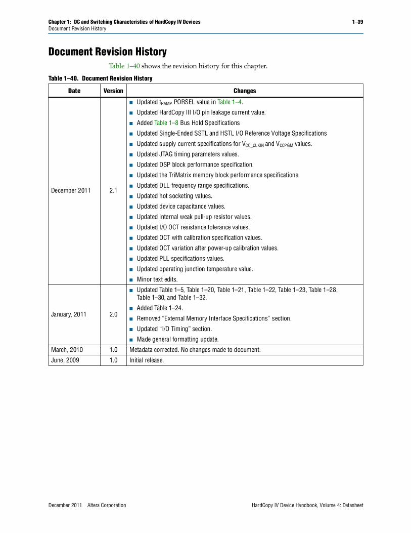
Document Revision HistoryTable 1–40 shows the revision history for this chapter.
Table 1–40. Document Revision History
Date Version Changes
December 2011 2.1
■ Updated tRAMP PORSEL value in Table 1–4.
■ Updated HardCopy III I/O pin leakage current value.
■ Added Table 1–8 Bus Hold Specifications
■ Updated Single-Ended SSTL and HSTL I/O Reference Voltage Specifications
■ Updated supply current specifications for VCC_CLKIN and VCCPGM values.
■ Updated JTAG timing parameters values.
■ Updated DSP block performance specification.
■ Updated the TriMatrix memory block performance specifications.
■ Updated DLL frequency range specifications.
■ Updated hot socketing values.
■ Updated device capacitance values.
■ Updated internal weak pull-up resistor values.
■ Updated I/O OCT resistance tolerance values.
■ Updated OCT with calibration specification values.
■ Updated OCT variation after power-up calibration values.
■ Updated PLL specifications values.
■ Updated operating junction temperature value.
■ Minor text edits.
January, 2011 2.0
■ Updated Table 1–5, Table 1–20, Table 1–21, Table 1–22, Table 1–23, Table 1–28, Table 1–30, and Table 1–32.
■ Added Table 1–24.
■ Removed “External Memory Interface Specifications” section.
■ Updated “I/O Timing” section.
■ Made general formatting update.
March, 2010 1.0 Metadata corrected. No changes made to document.
June, 2009 1.0 Initial release.

1–40 Chapter 1: DC and Switching Characteristics of HardCopy IV DevicesDocument Revision History
HardCopy IV Device Handbook, Volume 4: Datasheet December 2011 Altera Corporation