Embed Size (px)
Citation preview

TO-257 AA
D(1)
G(3)
S(2)SCO6140p
FeaturesVDS ID RDS(on) typ. Qg
100 V 12 A 265 mΩ 40 nC
• Fast switching• 100% avalanche tested• Hermetic package• 100 krad TID• SEE radiation hardened
DescriptionThis P-channel Power MOSFET is developed with STMicroelectronics uniqueSTripFET process. It has specifically been designed to sustain high TID and provideimmunity to heavy ion effects.
This Power MOSFET is fully ESCC qualified.
Product summaryProduct summary
Part
numbers
ESCC part
number
Quality
levelPackage
Lead
finishMass
Temp.
rangeEPPL
STRH12P10GY1Engineering
model
TO-257AA
Gold
5 g-55 to
150 °CSTRH12P10GYG 5205/029/01
ESCC
flightYes
STRH12P10GYT 5205/029/02Solder
dip
Note: Contact ST sales office for information about the specific conditionsfor product in die form and for other packages.
Product status link
STRH12P10
Rad-Hard P-channel, 100 V, 12 A Power MOSFET
STRH12P10
Datasheet
DS8699 - Rev 6 - May 2019For further information contact your local STMicroelectronics sales office.
www.st.com

1 Electrical ratings
TC= 25 °C unless otherwise specified
Table 1. Absolute maximum ratings (pre-irradiation)
Symbol Parameter Value Unit
VDS Drain-source voltage (VGS = 0) 100 V
VGS Gate-source voltage ±18 V
ID(1)Drain current (continuous) at Tcase = 25 °C 12 A
Drain current (continuous) at Tcase = 100 °C 7.5 A
IDM(2) Drain current (pulsed) 48 A
PTOT Total power dissipation at Tcase = 25 °C 75 W
dv/dt(3) Peak diode recovery voltage slope 2.4 V/ns
Tstg Storage temperature range -55 to 150 °C
Tj Max. operating junction temperature range 150 °C
1. Rated according to the Rthj-case + Rthc-s
2. Pulse width limited by safe operating area.3. ISD ≤ 12 A, di/dt ≤ 36 A/μs, VDD = 80 %V(BR)DSS.
Table 2. Thermal data
Symbol Parameter Value Unit
Rthj-case Thermal resistance junction-case max. 1.47 °C/W
Rthc-s Thermal resistance case-sink typ. 0.20 °C/W
Table 3. Avalanche characteristics
Symbol Parameter Value Unit
IARAvalanche current, repetitive or not-repetitive
(pulse width limited by Tj max)6 A
EAS(1)Single pulse avalanche energy
(starting Tj = 25 °C, ID = IAR, VDD = 50 V) at 110 °C112 mJ
EAR
Repetitive pulse avalanche energy
(VDS = 50 V, IAR = 6 A, f = 10 KHz,
TJ = 25 °C, duty cycle = 50%)
17 mJ
Repetitive pulse avalanche energy
(VDS = 50 V, IAR = 6 A, f = 10 KHz,
TJ = 110 °C, duty cycle = 50%)
5.5 mJ
1. Maximum rating value.
STRH12P10Electrical ratings
DS8699 - Rev 6 page 2/16

2 Electrical characteristics
TC = 25 °C unless otherwise specified
Table 4. Pre-irradiation on/off states
Symbol Parameter Test conditions Min. Typ. Max. Unit
IDSS Zero gate voltage drain current 80% V(BR)DSS 10 µA
IGSS Gate body leakage current
VGS = 16 V 100
nA
VGS = -16 V -100
VGS = 16 V,
TC = 125 °C200
VGS = -16 V,
TC = 125 °C-200
V(BR)DSS(1) Drain-to-source breakdownvoltage VGS = 0 V, ID = 1 mA 100 V
VGS(th) Gate threshold voltage
VDS = VGS, ID = 1 mA 2.0 4.5
VVDS = VGS, ID = 1 mA, TC = 125 °C 1.6 3.8
VDS = VGS, ID = 1 mA, TC = -55 °C 2.2 5.2
RDS(on) Static drain-source on resistance VGS = 12 V, ID = 12 A 0.265 0.30 Ω
1. This rating is guaranteed at TJ ≤ 25 °C (see Figure 9. Normalized V(BR)DSS vs temperature).
Table 5. Pre-irradation dynamic
Symbol Parameter Test conditions Min. Typ. Max. Unit
Ciss(1) Input capacitance
VDS = 25 V, f = 1 MHz, VGS = 0 V
940 1180 1410 pF
Coss Output capacitance 135 170 205 pF
Crss Reverse transfer capacitance 55 70 85 pF
Qg Total gate chargeVDD = 50 V, ID = 12 A,
VGS = 12 V
32 40 48 nC
Qgs Gate-to-source charge 3.5 5 6.5 nC
Qgd Gate-to-drain (“Miller”) charge 7 10 13 nC
1. Not tested, guaranteed by process.
Table 6. Pre-irradation switching times
Symbol Parameter Test conditions Min. Typ. Max. Unit
td(on) Turn-on delay time
VDD = 50 V, ID = 6 A, RG = 4.7 Ω,VGS = 12 V
5 9 13 ns
tr Rise time 7 19 31 ns
td(off) Turn-off delay time 18 30 42 ns
tf Fall time 3.5 7 10.5 ns
STRH12P10Electrical characteristics
DS8699 - Rev 6 page 3/16

Table 7. Pre-irradation source drain diode
Symbol Parameter Test conditions Min. Typ. Max. Unit
ISD Source-drain current 12 A
ISDM(1) Source-drain current (pulsed) 48 A
VSD (2) Forward on voltage
ISD = 12 A, VGS = 0 V 1.5
VISD = 12 A, VGS = 0 V,
TC = 125 °C1.25
trr Reverse recovery time ISD = 12 A, di/dt = 40 A/µs,
VDD = 60 V
Tj = 25 °C
178 218 258 ns
Qrr Reverse recovery charge 1700 2130 2560 nC
IRRM Reverse recovery current 14 19 24 A
trr Reverse recovery timeISD = 12 A, di/dt = 40 A/µs,
VDD = 60 V, TJ = 150 °C
225 280 335 ns
Qrr Reverse recovery charge 2650 3250 3950 nC
IRRM Reverse recovery current 18.5 23.5 28.5 A
1. Pulse width limited by safe operating area2. Pulsed: pulse duration = 300 µs, duty cycle 1.5%
Note: For Table 7. Pre-irradation source drain diode refer to Figure 13
STRH12P10Electrical characteristics
DS8699 - Rev 6 page 4/16
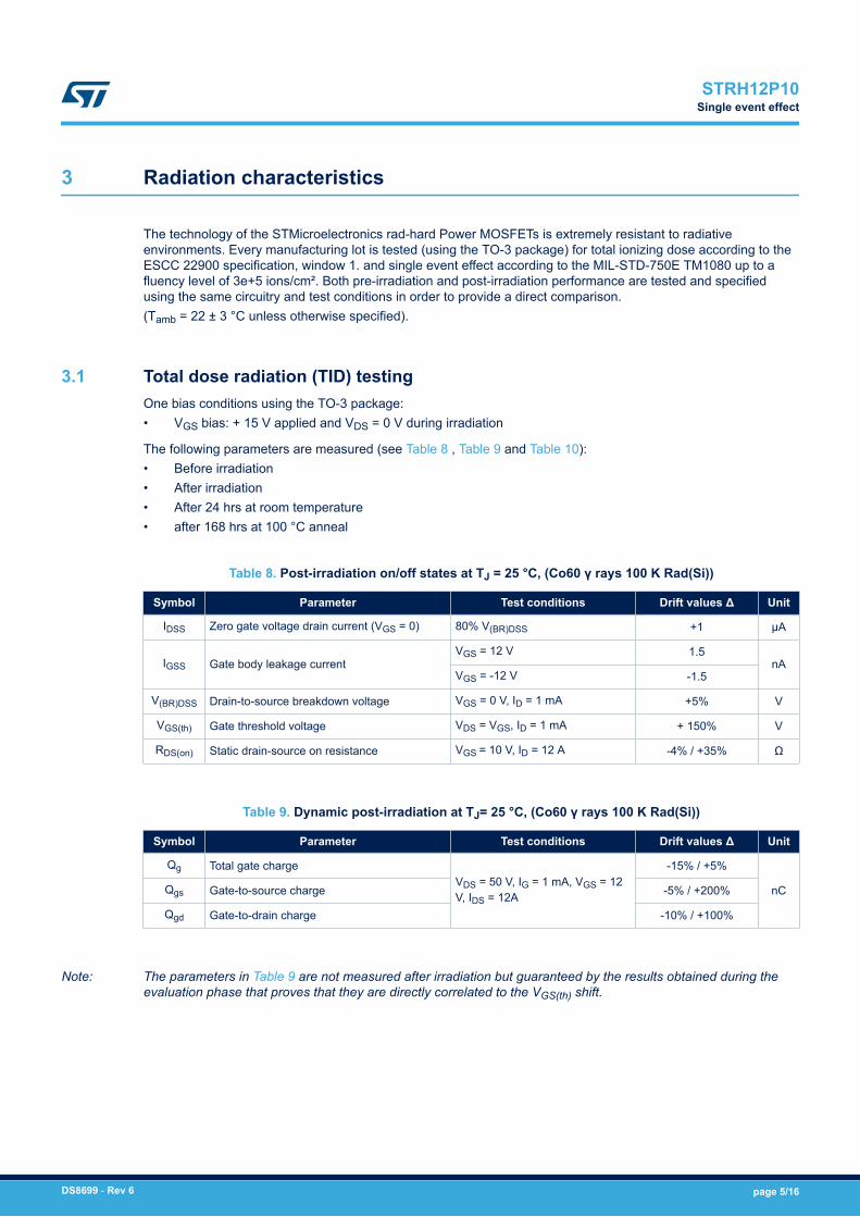
3 Radiation characteristics
The technology of the STMicroelectronics rad-hard Power MOSFETs is extremely resistant to radiativeenvironments. Every manufacturing lot is tested (using the TO-3 package) for total ionizing dose according to theESCC 22900 specification, window 1. and single event effect according to the MIL-STD-750E TM1080 up to afluency level of 3e+5 ions/cm². Both pre-irradiation and post-irradiation performance are tested and specifiedusing the same circuitry and test conditions in order to provide a direct comparison.(Tamb = 22 ± 3 °C unless otherwise specified).
3.1 Total dose radiation (TID) testingOne bias conditions using the TO-3 package:• VGS bias: + 15 V applied and VDS = 0 V during irradiation
The following parameters are measured (see Table 8 , Table 9 and Table 10):• Before irradiation• After irradiation• After 24 hrs at room temperature• after 168 hrs at 100 °C anneal
Table 8. Post-irradiation on/off states at TJ = 25 °C, (Co60 γ rays 100 K Rad(Si))
Symbol Parameter Test conditions Drift values Δ Unit
IDSS Zero gate voltage drain current (VGS = 0) 80% V(BR)DSS +1 µA
IGSS Gate body leakage currentVGS = 12 V 1.5
nAVGS = -12 V -1.5
V(BR)DSS Drain-to-source breakdown voltage VGS = 0 V, ID = 1 mA +5% V
VGS(th) Gate threshold voltage VDS = VGS, ID = 1 mA + 150% V
RDS(on) Static drain-source on resistance VGS = 10 V, ID = 12 A -4% / +35% Ω
Table 9. Dynamic post-irradiation at TJ= 25 °C, (Co60 γ rays 100 K Rad(Si))
Symbol Parameter Test conditions Drift values Δ Unit
Qg Total gate chargeVDS = 50 V, IG = 1 mA, VGS = 12V, IDS = 12A
-15% / +5%
nCQgs Gate-to-source charge -5% / +200%
Qgd Gate-to-drain charge -10% / +100%
Note: The parameters in Table 9 are not measured after irradiation but guaranteed by the results obtained during theevaluation phase that proves that they are directly correlated to the VGS(th) shift.
STRH12P10Single event effect
DS8699 - Rev 6 page 5/16

Table 10. Source drain diode post-irradiation at TJ= 25 °C, (Co60 γ rays 100 K Rad(Si))
Symbol Parameter Test conditions Drift values Δ Unit
VDS (1) Forward on voltage VGS = 0 V, ISD = 40 A ±5% V
1. Pulsed: pulse duration = 300 μs, duty cycle 1.5%
Note: For Table 10 refer to Figure 15.
3.2 Single event effect SOAThe technology of the STMicroelectronics rad-hard Power MOSFETs is extremely resistant to heavy ionenvironment for single event effect (irradiation per MIL-STD-750E, method 1080 bias circuit in Figure 2. Singleevent effect, bias circuit). SEB and SEGR tests have been performed with a fluence of 3e+5 ions/cm².The accept/reject criteria are :• SEB (test):
drain voltage checked, trigger level is set to VDS = - 5 V. Stop condition: as soon as a SEB occurs or if thefluence reaches 3e+5 ions/cm².
• SEGR test:the gate current is monitored every 200 ms. A gate stress is performed before and after irradiation. Stopcondition: as soon as the gate current reaches 100 nA (during irradiation or during PIGS test) or if thefluence reaches 3e+5 ions/cm².
The results are:• no SEB• SEGR immune at 60 MeV/mg/cm2 within the safe operating area (SOA) given in Table 11. Single event
effect (SEE), safe operating area (SOA) and Figure 1. Single event effect, SOA.
Table 11. Single event effect (SEE), safe operating area (SOA)
Ion Let (Mev/(mg/cm2)Energy
(MeV)
Range
(μm)
VDS (V)
at VGS=0 V at VGS= 2 V at VGS= 5 V at VGS= 10 V at VGS= 15 V
Kr 32768 94 - -60 - - -
756 92 - - - - -20
Cu 28 285 43 -100 - -60 - -
Xe 60 1217 89 - -30 - - -
STRH12P10Single event effect,SOA
DS8699 - Rev 6 page 6/16

Figure 1. Single event effect, SOA
0
10
20
30
40
50
60
70
80
90
100
0 5 10 15 20
VD
S(%
VD
Sm
ax)
VGS(V)
Cu (28 MeV.cm2/mg)
Kr (32 MeV.cm2/mg)
Xe (60 MeV.cm2/mg)
Figure 2. Single event effect, bias circuit
R4 R3
C4270 270
820 pF
U2Vgs
C5220 nF
C64.7 µF
Vds
AM09224v1
Ω Ω
Note: Bias condition during radiation refer to Table 11. Single event effect (SEE), safe operating area (SOA).
STRH12P10Single event effect,SOA
DS8699 - Rev 6 page 7/16

4 Electrical characteristics (curves)
Figure 3. Safe operating area
ID
10.00
1.00
0.1 1 100 VDS(V)10
(A)
Operat
ion in
this
area i
s
Limite
d by m
ax RDS(
on) 100µs
1ms
10ms
0.10
Tj=150°CTc=25°CSingle pulse
AM16049v1
Figure 4. Thermal impedance
Figure 5. Output characteristics Figure 6. Transfer characteristics
Figure 7. Gate charge vs gate-source voltage Figure 8. Capacitance variations
STRH12P10Electrical characteristics (curves)
DS8699 - Rev 6 page 8/16

Figure 9. Normalized V(BR)DSS vs temperature Figure 10. Static drain-source on-resistance
Figure 11. Normalized gate threshold voltage vstemperature Figure 12. Normalized on-resistance vs temperature
Figure 13. Source drain-diode forward characteristics
STRH12P10Electrical characteristics (curves)
DS8699 - Rev 6 page 9/16

5 Test circuits
Figure 14. Switching times test circuit for resistive load
Note: Max driver VGS slope = 1V/ns (no DUT)
Figure 15. Source drain diode
trr
ba
10[%] of IRM
di/dt
Body diode reverse current, I RM
IFM body diode forward current
AM092225V1
Figure 16. Unclamped inductive load test circuit (single pulse and repetitive)
STRH12P10Test circuits
DS8699 - Rev 6 page 10/16

6 Package information
In order to meet environmental requirements, ST offers these devices in different grades of ECOPACK packages,depending on their level of environmental compliance. ECOPACK specifications, grade definitions and productstatus are available at: www.st.com. ECOPACK is an ST trademark.
6.1 TO-257AA package information
Figure 17. TO-257AA package outline
0117268_E
STRH12P10Package information
DS8699 - Rev 6 page 11/16

Table 12. TO-257AA package mechanical data
SymbolsDimensions (mm) Dimensions (inches)
Min. Typ. Max. Min. Typ. Max.
A 4.83 5.08 0.190 0.200
A1 0.89 1.14 0.035 0.045
A2 3.05 0.120
b 0.64 1.02 0.025 0.040
b1 0.64 0.76 0.89 0.025 0.030 0.035
D 16.38 16.89 0.645 0.665
D1 10.41 10.92 0.410 0.430
D2 - - 0.97 0.038
e 2.54 0.100
E 10.41 10.67 0.410 0.420
L 15.24 16.51 0.600 0.650
L1 13.39 13.64 0.527 0.537
P 3.56 3.81 0.140 0.150
STRH12P10TO-257AA package information
DS8699 - Rev 6 page 12/16

7 Order codes
Table 13. Ordering information
Order codesESCC part
numberQuality level EPPL Package
Lead
finishMarking Packing
STRH12P10GY1 -Engineering
model-
TO-257AA
Gold
STRH12P10GY1
+ BeO
Strip packSTRH12P10GYG 5205/029/01
ESCC flight
Yes520502901R
+ BeO
STRH12P10GYT 5205/029/02 YesSolder
dip
520502902R
+ BeO
For specific marking only the complete structure is:• ST Logo• ESA Logo• Date code (date of sealing of the package) : YYWWA
– YY: year– WW: week number– A: week index
• ESCC part number (as mentioned in the table)• Warning signs (e.g. BeO)• Country of origin: FR (France)• Part serial number within in the assembly lot
Contact ST sales office for information about the specific conditions for products in die form and for otherpackages.
STRH12P10Order codes
DS8699 - Rev 6 page 13/16
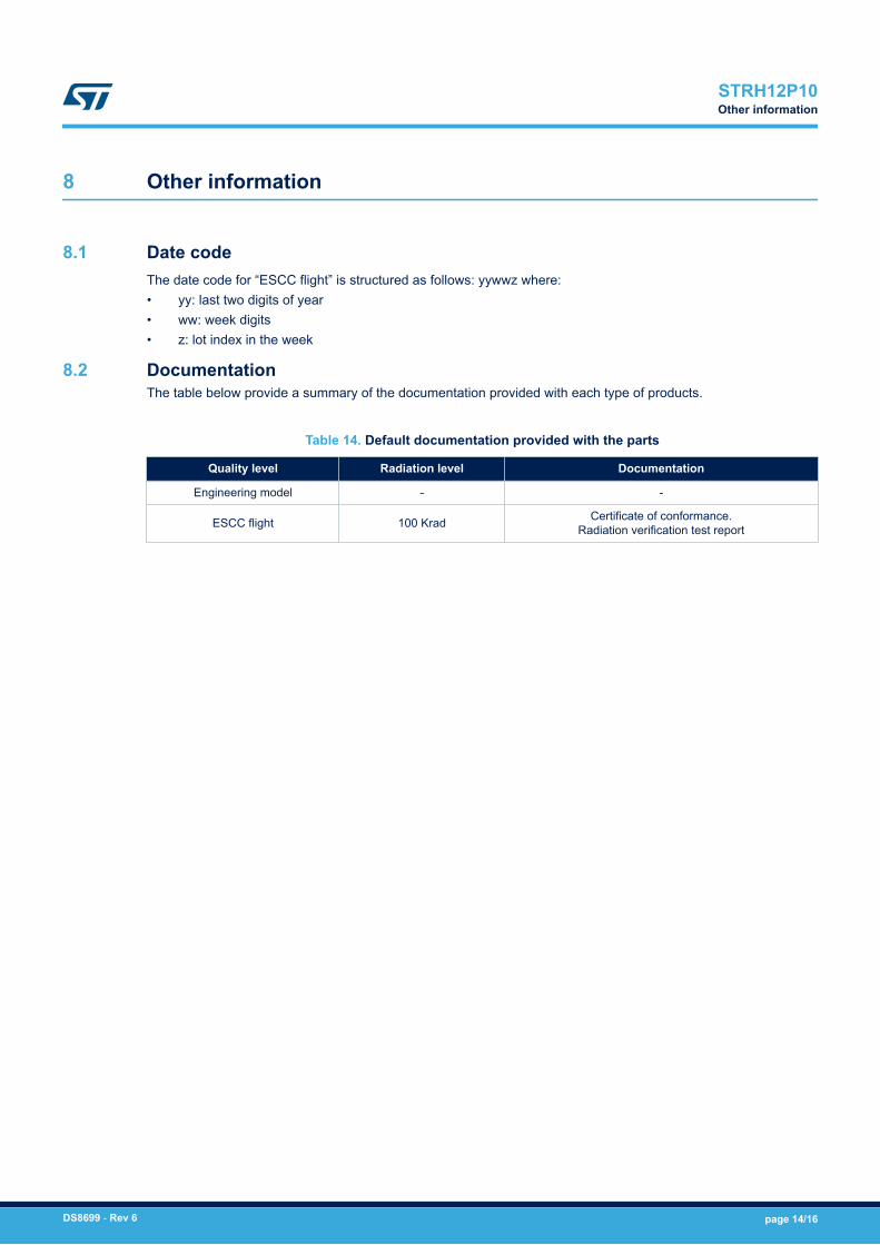
8 Other information
8.1 Date codeThe date code for “ESCC flight” is structured as follows: yywwz where:• yy: last two digits of year• ww: week digits• z: lot index in the week
8.2 DocumentationThe table below provide a summary of the documentation provided with each type of products.
Table 14. Default documentation provided with the parts
Quality level Radiation level Documentation
Engineering model - -
ESCC flight 100 Krad Certificate of conformance.Radiation verification test report
STRH12P10Other information
DS8699 - Rev 6 page 14/16

Revision history
Table 15. Document revision history
Date Version Changes
07-Oct-2011 1 First release.
24-Jun-2013 2
Document status promoted form preliminary data to production data.
– Modified: Figure 1
– Modified: EAS, EAR parameter and values in Table 4
– Modified: IGSS, and added note 1 in Table 5
– Added: note 1 in Table 6
– Modified: trr, qrr and IRRM parameter in Table 8
– Modified: RDS(on) test conditions in Table 9, the entire test conditions inTable 10
– Modified: Figure 4
25-Nov-2013 3 – Modified: package drawing and Figure 1.
18-Dec-2013 4– Updated Table 1: Device summary and Table 14: Ordering information.
– Updated Section : Total dose radiation (TID) testing.
19-Jan-2015 5– Updated Table 13.: TO-257AA mechanical data
– Minor text changes
02-May-2019 6Updated Table 7. Pre-irradation source drain diode and Table 4. Pre-irradiation on/off states.Minor text changes.
STRH12P10
DS8699 - Rev 6 page 15/16

IMPORTANT NOTICE – PLEASE READ CAREFULLY
STMicroelectronics NV and its subsidiaries (“ST”) reserve the right to make changes, corrections, enhancements, modifications, and improvements to STproducts and/or to this document at any time without notice. Purchasers should obtain the latest relevant information on ST products before placing orders. STproducts are sold pursuant to ST’s terms and conditions of sale in place at the time of order acknowledgement.
Purchasers are solely responsible for the choice, selection, and use of ST products and ST assumes no liability for application assistance or the design ofPurchasers’ products.
No license, express or implied, to any intellectual property right is granted by ST herein.
Resale of ST products with provisions different from the information set forth herein shall void any warranty granted by ST for such product.
ST and the ST logo are trademarks of ST. For additional information about ST trademarks, please refer to www.st.com/trademarks. All other product or servicenames are the property of their respective owners.
Information in this document supersedes and replaces information previously supplied in any prior versions of this document.
© 2019 STMicroelectronics – All rights reserved
STRH12P10
DS8699 - Rev 6 page 16/16