Embed Size (px)
Citation preview

DPAK
K
NCA
D²PAK HV
A K
AK
K
NC
A
Product label
Features
• AEC-Q101 qualified • No reverse recovery charge in application current range• Switching behavior independent of temperature• Recommended to PFC applications• PPAP capable• VRRM guaranteed from -40 to 175 °C• D²PAK HV creepage distance (anode to cathode) = 5.38 mm min. (with top
coating)• ECOPACK®2 compliant component
Applications• On board charger
DescriptionThe SiC diode is an ultra-high performance power Schottky diode. It is manufacturedusing a silicon carbide substrate. The wide band gap material allows the design of aSchottky diode structure with a 650 V rating. Due to the Schottky construction, norecovery is shown at turn-off and ringing patterns are negligible. The minimalcapacitive turn-off behavior is independent of temperature.
Especially suited for use in PFC applications, the STPSC8H065-Y SiC diode willboost performance in hard switching conditions.
Product status
STPSC8H065-Y
Product summary
Symbol Value
IF(AV) 8 A
VRRM 650 V
Tj(max.) 175 °C
Automotive 650 V, 8 A high surge silicon carbide power Schottky diode
STPSC8H065-Y
Datasheet
DS12495 - Rev 3 - December 2018For further information contact your local STMicroelectronics sales office.
www.st.com

1 Characteristics
Table 1. Absolute ratings (limiting values at 25 °C unless otherwise specified)
Symbol Parameter Value Unit
VRRM Repetitive peak reverse voltage Tj = -40 °C to + 175 °C 650 V
IF(RMS) Forward rms current 22 A
IF(AV) Average forward current Tc = 145 °C(1), DC 8 A
IFSM Surge non repetitive forward current
tp = 10 ms sinusoidal, Tc = 25 °C
tp = 10 ms sinusoidal, Tc = 125 °C
tp = 10 µs square, Tc = 25 °C
75
69
420
A
IFRM Repetitive peak forward current Tc = 145 °C (1), Tj = 175 °C, δ = 0.1 33 A
Tstg Storage temperature range -55 to +175 °C
Tj Operating junction temperature range -40 to +175 °C
1. Value based on Rth(j-c) max.
Table 2. Thermal resistance parameters
Symbol Parameter Typ. value Max. value Unit
Rth(j-c) Junction to case 1.3 1.6 °C/W
Table 3. Static electrical characteristics
Symbol Parameter Test conditions Min. Typ. Max. Unit
IR(1) Reverse leakage currentTj = 25 °C
VR = VRRM- 7 80
µATj = 150 °C - 65 335
VF(2) Forward voltage dropTj = 25 °C
IF = 8 A- 1.45 1.65
VTj = 150 °C - 1.7 2.05
1. tp = 10 ms, δ < 2%
2. tp = 500 μs, δ < 2%
To evaluate the conduction losses, use the following equation:P = 0.972 x IF(AV) + 0.135 x IF2(RMS)
Table 4. Dynamic electrical characteristics
Symbol Parameter Test conditions Typ. Unit
Qcj(1) Total capacitive charge VR = 400 V 23.5 nC
Cj Total capacitanceVR = 0 V, Tc = 25 °C, F = 1 MHz 414
pFVR = 400 V, Tc = 25 °C, F = 1 MHz 38
1.Most accurate value for the capacitive charge: Qcj VR = ∫0VRCj V dV
STPSC8H065-YCharacteristics
DS12495 - Rev 3 page 2/12
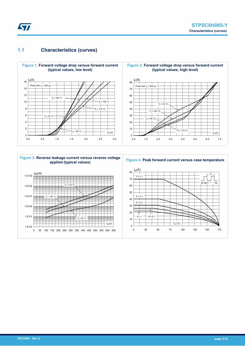
1.1 Characteristics (curves)
Figure 1. Forward voltage drop versus forward current(typical values, low level)
0
2
4
6
8
10
12
14
16
0.0 0.5 1.0 1.5 2.0 2.5 3.0
VF(V)
IF(A)
Ta = 150 °C
Ta = 175 °C
Ta = 25 °C
Pulse test: tp = 500 µs
Ta = 100 °C
Ta = -40 °C
Figure 2. Forward voltage drop versus forward current(typical values, high level)
IF(A)
0
10
20
30
40
50
60
70
80
0.0 1.0 2.0 3.0 4.0 5.0 6.0 7.0
VF(V)
Pulse test: tp = 500 µs
Ta = 150 °C
Ta = 175 °C
Ta = 25 °C
Ta = 100 °C
Figure 3. Reverse leakage current versus reverse voltageapplied (typical values)
1.E-02
1.E-01
1.E+00
1.E+01
1.E+02
1.E+03
0 50 100 150 200 250 300 350 400 450 500 550 600 650
VR(V)
IR(µA)
Tj = 25 °C
Tj = 150 °C
Tj = 175 °C
Figure 4. Peak forward current versus case temperature
0
10
20
30
40
50
60
70
80
0 25 50 75 100 125 150 175
TC(°C)
IM(A)T
δ=tp/T tp
δ = 0.1
δ = 0.3
δ = 0.5
δ = 1 δ = 0.7
STPSC8H065-YCharacteristics (curves)
DS12495 - Rev 3 page 3/12

Figure 5. Junction capacitance versus reverse voltageapplied (typical values)
0
50
100
150
200
250
300
350
400
450
500
0.1 1.0 10.0 100.0 1000.0
VR(V)
Cj(pF)
F = 1 MHzVOSC = 30 mVRMS
Tj = 25 °C
Figure 6. Relative variation of thermal impedance junctionto case versus pulse duration
0.0
0.1
0.2
0.3
0.4
0.5
0.6
0.7
0.8
0.9
1.0
1.E-05 1.E-04 1.E-03 1.E-02 1.E-01 1.E+00
tp(s)
Zth(j-c) /Rth(j-c)
Single pulse
Figure 7. Non-repetitive peak surge forward currentversus pulse duration (sinusoidal waveform)
1.E+01
1.E+02
1.E+03
1.E-05 1.E-04 1.E-03 1.E-02
tp(s)
IFSM(A)
Ta = 25 °C
Ta = 125 °C
Figure 8. Total capacitive charges versus reverse voltageapplied (typical values)
0
4
8
12
16
20
24
28
0 50 100 150 200 250 300 350 400
VR(V)
QCj(nC)
Figure 9. Thermal resistance junction to ambient versus copper surface under tab (typical values, epoxyprinted board FR4, eCu = 35 µm) (D²PAK-HV)
0
10
20
30
40
50
60
70
80
0 5 10 15 20 25 30 35 40
Rth(j-a) (°C/W)
D²PAK -HV
SCu(cm²)
STPSC8H065-YCharacteristics (curves)
DS12495 - Rev 3 page 4/12

2 Package information
In order to meet environmental requirements, ST offers these devices in different grades of ECOPACK®
packages, depending on their level of environmental compliance. ECOPACK® specifications, grade definitionsand product status are available at: www.st.com. ECOPACK® is an ST trademark.
2.1 DPAK package information• Epoxy meets UL94, V0• Lead-free packages
Figure 10. DPAK package outline
E
b4
L2
H L4
A
c2
D
A1
R
c
b (2x)e
e1
A2
L(L1)
V2
E1
D1
Gauge plane
Seating plane
0.25
STPSC8H065-YPackage information
DS12495 - Rev 3 page 5/12

Table 5. DPAK mechanical data
Dim.
Dimensions
Millimeters Inches(1)
Min. Typ. Max. Min. Typ. Max.
A 2.20 2.40 0.087 0.094
A1 0.90 1.10 0.035 0.043
A2 0.03 0.23 0.001 0.009
b 0.64 0.90 0.025 0.035
b4 5.20 5.40 0.205 0.213
c 0.45 0.60 0.018 0.024
c2 0.48 0.60 0.019 0.024
D 6.00 6.20 0.236 0.244
D1 4.95 5.10 5.25 0.195 0.201 0.207
E 6.40 6.60 0.252 0.260
E1 4.60 4.70 4.80 0.181 0.185 0.189
e 2.159 2.286 2.413 0.085 0.090 0.095
e1 4.445 4.572 4.699 0.175 0.180 0.185
H 9.35 10.10 0.368 0.398
L 1.00 1.50 0.039 0.059
(L1) 2.60 2.80 3.00 0.102 0.110 0.118
L2 0.65 0.80 0.95 0.026 0.031 0.037
L4 0.60 1.00 0.024 0.039
R 0.20 0.008
V2 0° 8° 0° 8°
1. Inches dimensions given for reference only
Figure 11. DPAK recommended footprint (dimensions are in mm)
The device must be positioned within
6.3
6.110.7
1.54.572
A
B
2.8
1.8
min
.
STPSC8H065-YDPAK package information
DS12495 - Rev 3 page 6/12

2.2 D²PAK HV package information
Figure 12. D²PAK high voltage package outline
H
L4
L
F (x2)
e
L1
AC
L2
R
M R
0.25 gauge plane
E
A1
V
H1
L3
STPSC8H065-YD²PAK high voltage package information
DS12495 - Rev 3 page 7/12

Table 6. D²PAK high voltage package mechanical data
Ref.Dimensions
Min. Typ. Max.
A 4.30 4.70
A1 0.03 0.20
C 1.17 1.37
e 4.98 5.18
E 0.50 0.90
F 0.78 0.85
H 10.00 10.40
H1 7.40 7.80
L 15.30 15.80
L1 1.27 1.40
L2 4.93 5.23
L3 6.85 7.25
L4 1.5 1.7
M 2.6 2.9
R 0.20 0.60
V 0° 8°
Figure 13. D²PAK High Voltage footprint in mm
15,95
7,46
3,40
5,081,20
10,58
5,10
STPSC8H065-YD²PAK high voltage package information
DS12495 - Rev 3 page 8/12

2.2.1 Creepage distance between anode and cathode
Table 7. Creepage distance between anode and cathode
Symbol Parameter Value Unit
CdA-K1 Minimum creepage distance between A and K1 (with top coating)D²PAK HV
5.38mm
CdA-K2 Minimum creepage distance between A and K2 (without top coating) 3.48
Note: D²PAK HV creepage distance (anode to cathode) = 5.38 mm min. (refer to IEC 60664-1)
Figure 14. Creepage with top coating
Figure 15. Creepage without top coating
STPSC8H065-YD²PAK high voltage package information
DS12495 - Rev 3 page 9/12
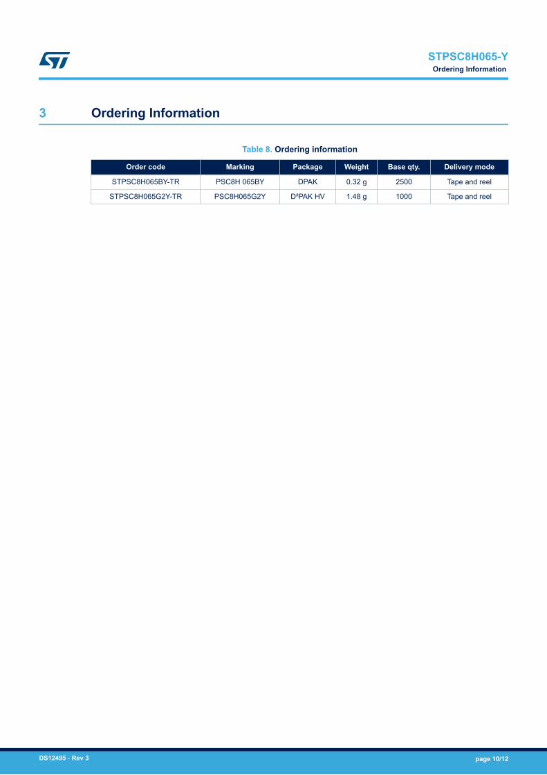
3 Ordering Information
Table 8. Ordering information
Order code Marking Package Weight Base qty. Delivery mode
STPSC8H065BY-TR PSC8H 065BY DPAK 0.32 g 2500 Tape and reel
STPSC8H065G2Y-TR PSC8H065G2Y D²PAK HV 1.48 g 1000 Tape and reel
STPSC8H065-YOrdering Information
DS12495 - Rev 3 page 10/12

Revision history
Table 9. Document revision history
Date Version Changes
08-Mar-2018 1 Initial release.
11-Sep-2018 2 Added D²PAK HV package.
06-Dec-2018 3
Updated Section 2.2.1 Creepage distance between anode and cathode.
Minor text changes to improve readability.
Updated title of document.
STPSC8H065-Y
DS12495 - Rev 3 page 11/12

IMPORTANT NOTICE – PLEASE READ CAREFULLY
STMicroelectronics NV and its subsidiaries (“ST”) reserve the right to make changes, corrections, enhancements, modifications, and improvements to STproducts and/or to this document at any time without notice. Purchasers should obtain the latest relevant information on ST products before placing orders. STproducts are sold pursuant to ST’s terms and conditions of sale in place at the time of order acknowledgement.
Purchasers are solely responsible for the choice, selection, and use of ST products and ST assumes no liability for application assistance or the design ofPurchasers’ products.
No license, express or implied, to any intellectual property right is granted by ST herein.
Resale of ST products with provisions different from the information set forth herein shall void any warranty granted by ST for such product.
ST and the ST logo are trademarks of ST. All other product or service names are the property of their respective owners.
Information in this document supersedes and replaces information previously supplied in any prior versions of this document.
© 2018 STMicroelectronics – All rights reserved
STPSC8H065-Y
DS12495 - Rev 3 page 12/12