Embed Size (px)
Citation preview
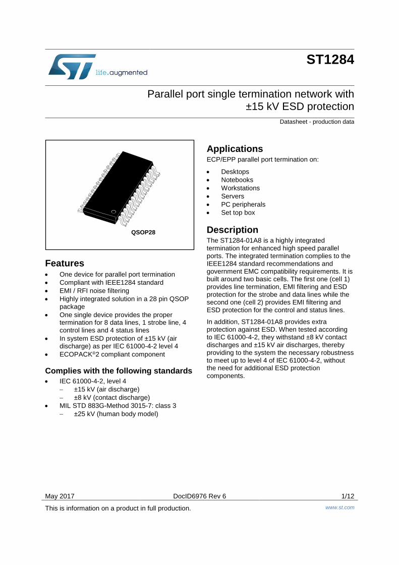
May 2017 DocID6976 Rev 6 1/12
This is information on a product in full production. www.st.com
ST1284
Parallel port single termination network with ±15 kV ESD protection
Datasheet - production data
Features One device for parallel port termination
Compliant with IEEE1284 standard
EMI / RFI noise filtering
Highly integrated solution in a 28 pin QSOP package
One single device provides the proper termination for 8 data lines, 1 strobe line, 4 control lines and 4 status lines
In system ESD protection of ±15 kV (air discharge) as per IEC 61000-4-2 level 4
ECOPACK®2 compliant component
Complies with the following standards
IEC 61000-4-2, level 4
±15 kV (air discharge)
±8 kV (contact discharge)
MIL STD 883G-Method 3015-7: class 3
±25 kV (human body model)
Applications ECP/EPP parallel port termination on:
Desktops
Notebooks
Workstations
Servers
PC peripherals
Set top box
Description The ST1284-01A8 is a highly integrated termination for enhanced high speed parallel ports. The integrated termination complies to the IEEE1284 standard recommendations and government EMC compatibility requirements. It is built around two basic cells. The first one (cell 1) provides line termination, EMI filtering and ESD protection for the strobe and data lines while the second one (cell 2) provides EMI filtering and ESD protection for the control and status lines.
In addition, ST1284-01A8 provides extra protection against ESD. When tested according to IEC 61000-4-2, they withstand ±8 kV contact discharges and ±15 kV air discharges, thereby providing to the system the necessary robustness to meet up to level 4 of IEC 61000-4-2, without the need for additional ESD protection components.
QSOP28
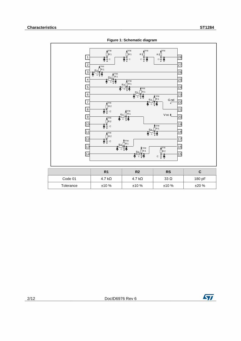
Characteristics ST1284
2/12 DocID6976 Rev 6
Figure 1: Schematic diagram
R1 R2 RS C
Code 01 4.7 kΩ 4.7 kΩ 33 Ω 180 pF
Tolerance ±10 % ±10 % ±10 % ±20 %
28
27
26
25
24
23
22
21
20
19
18
17
16
1514
13
12
11
10
9
8
7
6
5
4
3
2
1
Vcc Vcc VccVcc
Vcc
Vcc
Vcc
Vcc
Vcc
Vcc
Vcc
Vcc
Vcc
Gnd
VccVcc
Vcc
Vcc
Vcc
R1
C
R1
C
R1 R2
C
R1
R1
R1
R1
R1
R2
R1
R2
R1
R2
R1
R1 R2
C
Rs
C
Rs
C
Rs
C
Rs
C
Rs
C
Rs
C
Rs
C
Rs
Rs
C
C
C
C
C C
ST1284 Characteristics
DocID6976 Rev 6 3/12
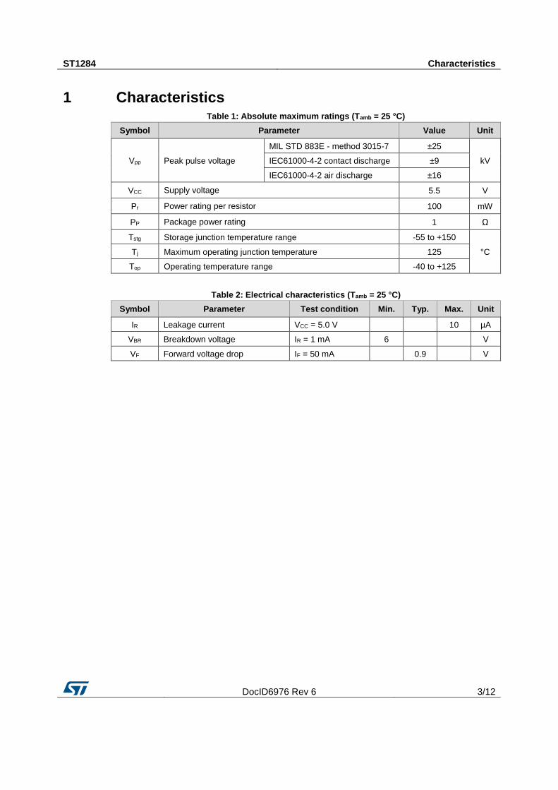
1 Characteristics Table 1: Absolute maximum ratings (Tamb = 25 °C)
Symbol Parameter Value Unit
Vpp Peak pulse voltage
MIL STD 883E - method 3015-7 ±25
kV IEC61000-4-2 contact discharge ±9
IEC61000-4-2 air discharge ±16
VCC Supply voltage 5.5 V
Pr Power rating per resistor 100 mW
PP Package power rating 1 Ω
Tstg Storage junction temperature range -55 to +150
°C Tj Maximum operating junction temperature 125
Top Operating temperature range -40 to +125
Table 2: Electrical characteristics (Tamb = 25 °C)
Symbol Parameter Test condition Min. Typ. Max. Unit
IR Leakage current VCC = 5.0 V
10 µA
VBR Breakdown voltage IR = 1 mA 6
V
VF Forward voltage drop IF = 50 mA
0.9
V
Characteristics ST1284
4/12 DocID6976 Rev 6
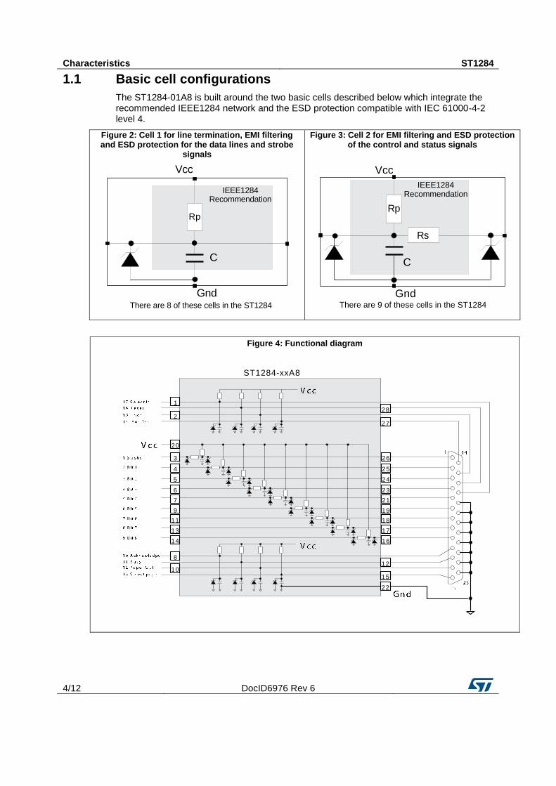
1.1 Basic cell configurations
The ST1284-01A8 is built around the two basic cells described below which integrate the recommended IEEE1284 network and the ESD protection compatible with IEC 61000-4-2 level 4.
Figure 2: Cell 1 for line termination, EMI filtering and ESD protection for the data lines and strobe
signals
Figure 3: Cell 2 for EMI filtering and ESD protection of the control and status signals
Figure 4: Functional diagram
C
IEEE1284Recommendation
Vcc
Gnd
Rp
There are 8 of these cells in the ST1284
C
IEEE1284Recommendation
Vcc
Gnd
Rp
Rs
There are 9 of these cells in the ST1284
128
227
20
26
25
24
23
21
19
18
17
16
3
4
5
6
7
9
11
13
14
8
1012
15
22
ST1284-xxA8
ST1284 Application information
DocID6976 Rev 6 5/12
2 Application information
The functional diagram here above presents a IEEE1284-A connector pinout and shows how to connect the ST1284-01A8 in order to correctly terminate and filter the 17 signal lines. The IEEE1284-A connector is the PC standard for the host connection.
Control and status lines (from 10 to 17) only require a pull-up resistor (Rp) and a filter capacitor (C).
The data lines (from 2 to 9) and the STROBE (pin 1) also require a termination series resistor (Rs) in addition to the pull-up resistor and a filter capacitor. The VCC is connected to pin 20 and the ground to pin 22.
The ST1284-01A8 can be used with all 3 types of connectors defined in the IEEE1284 standard:
IEEE1284-A is a 25 dB connector which is the PC standard for the host connection.
IEEE1284-B is a 36 pin, 0.085 inch center line connector used on the peripheral device.
IEEE1284-C is a new 36 pin, 0.050 inch center line connector which can be used for both host and peripherals.
Technical information ST1284
6/12 DocID6976 Rev 6
3 Technical information
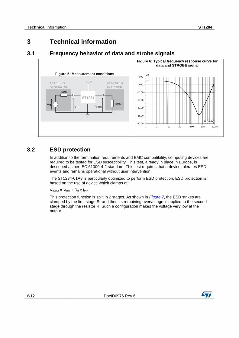
3.1 Frequency behavior of data and strobe signals
Figure 5: Measurement conditions
Figure 6: Typical frequency response curve for data and STROBE signal
3.2 ESD protection
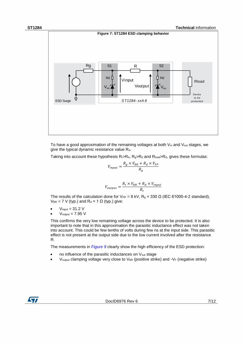
In addition to the termination requirements and EMC compatibility, computing devices are required to be tested for ESD susceptibility. This test, already in place in Europe, is described as per IEC 61000-4-2 standard. This test requires that a device tolerates ESD events and remains operational without user intervention.
The ST1284-01A8 is particularly optimized to perform ESD protection. ESD protection is based on the use of device which clamps at:
Vouput = VBR + Rd x IPP
This protection function is split in 2 stages. As shown in Figure 7, the ESD strikes are clamped by the first stage S1 and then its remaining overvoltage is applied to the second stage through the resistor R. Such a configuration makes the voltage very low at the output.
ST1284
SPECTRUM
ANALYSER
TRACKING
GENERATOR
V gVoutV in
50W
50W
+5 V
1 3 10 30 100 300 1,000
-30.00
-25.00
-20.00
-15.00
-10.00
-5.00
0.00dB
F (MHz)
ST1284 Technical information
DocID6976 Rev 6 7/12
Figure 7: ST1284 ESD clamping behavior
To have a good approximation of the remaining voltages at both Vin and Vout stages, we give the typical dynamic resistance value Rd.
Taking into account these hypothesis Rt>Rd, Rg>Rd and Rload>Rd, gives these formulas:
𝑉𝑖𝑛𝑝𝑢𝑡 =𝑅𝑔 × 𝑉𝐵𝑅 + 𝑅𝑑 × 𝑉𝑃𝑃
𝑅𝑔
𝑉𝑜𝑢𝑡𝑝𝑢𝑡 =𝑅𝑡 × 𝑉𝐵𝑅 + 𝑅𝑑 × 𝑉𝑖𝑛𝑝𝑢𝑡
𝑅𝑡
The results of the calculation done for VPP = 8 kV, Rg = 330 Ω (IEC 61000-4-2 standard), VBR = 7 V (typ.) and Rd = 1 Ω (typ.) give:
Vinput = 31.2 V
Voutput = 7.95 V
This confirms the very low remaining voltage across the device to be protected. It is also important to note that in this approximation the parasitic inductance effect was not taken into account. This could be few tenths of volts during few ns at the input side. This parasitic effect is not present at the output side due to the low current involved after the resistance R.
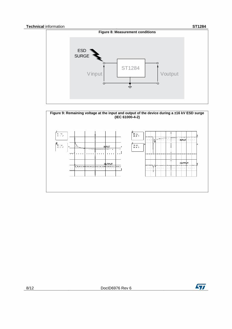
The measurements in Figure 9 clearly show the high efficiency of the ESD protection:
no influence of the parasitic inductances on Vout stage
Voutput clamping voltage very close to VBR (positive strike) and -VF (negative strike)
ESD Surge
Vinput
VoutputRload
Rg RS1
Rd
VBR VBR
Device
to be
protectedS T1284- xxA 8
Rd
S2
Technical information ST1284
8/12 DocID6976 Rev 6
Figure 8: Measurement conditions
Figure 9: Remaining voltage at the input and output of the device during a ±16 kV ESD surge (IEC 61000-4-2)
ST1284Vinput Voutput
ESD
SURGE
ST1284 Package information
DocID6976 Rev 6 9/12
4 Package information
In order to meet environmental requirements, ST offers these devices in different grades of ECOPACK® packages, depending on their level of environmental compliance. ECOPACK® specifications, grade definitions and product status are available at: www.st.com. ECOPACK® is an ST trademark.
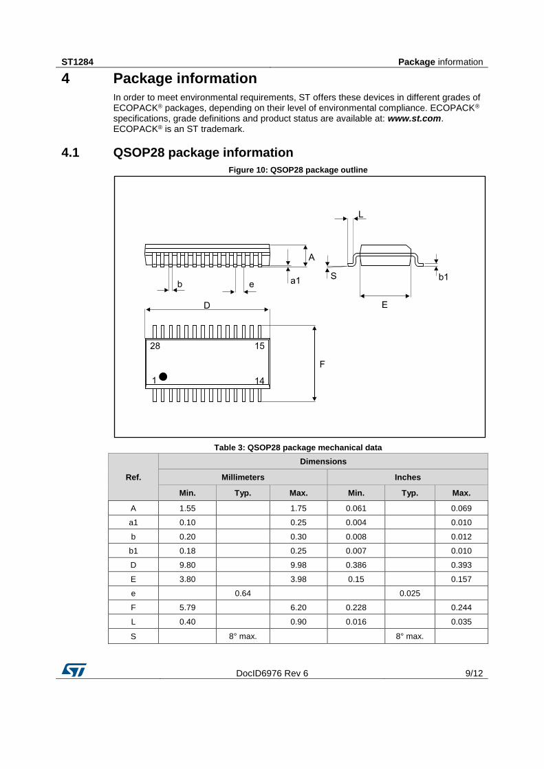
4.1 QSOP28 package information
Figure 10: QSOP28 package outline
Table 3: QSOP28 package mechanical data
Ref.
Dimensions
Millimeters Inches
Min. Typ. Max. Min. Typ. Max.
A 1.55
1.75 0.061
0.069
a1 0.10
0.25 0.004
0.010
b 0.20
0.30 0.008
0.012
b1 0.18
0.25 0.007
0.010
D 9.80
9.98 0.386
0.393
E 3.80
3.98 0.15
0.157
e
0.64
0.025
F 5.79
6.20 0.228
0.244
L 0.40
0.90 0.016
0.035
S
8° max.
8° max.
Package information ST1284
10/12 DocID6976 Rev 6
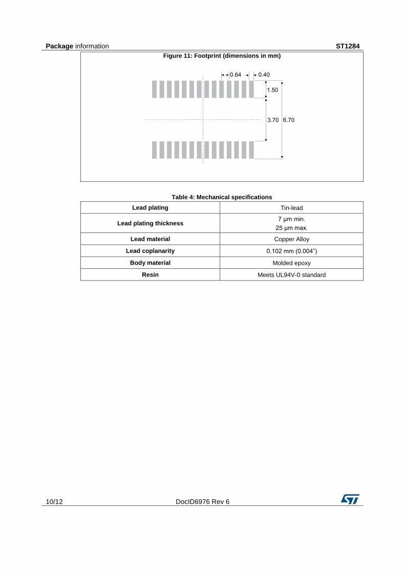
Figure 11: Footprint (dimensions in mm)
Table 4: Mechanical specifications
Lead plating Tin-lead
Lead plating thickness 7 μm min.
25 μm max.
Lead material Copper Alloy
Lead coplanarity 0.102 mm (0.004”)
Body material Molded epoxy
Resin Meets UL94V-0 standard
ST1284 Ordering information
DocID6976 Rev 6 11/12
5 Ordering information Table 5: Ordering information
Order code Marking Package Weight Base qty. Delivery mode
ST1284-01A8 ST1284-01 QSOP28 0.147 g
48 Tube
ST1284-01A8RL 2500 Tape and reel
6 Revision history Table 6: Document revision history
Date Revision Changes
Oct-2003 2B Last release.
12-Mar-2010 3 Updated table in Figure 1 and Figure 10.
11-May-2012 4 Updated Table 3.
09-Jul-2014 5 Corrected typographical error in Table 2.
05-May-2017 6 Updated Table 1: "Absolute maximum ratings (Tamb = 25 °C)".
Minor text changes to improve readability.
ST1284
12/12 DocID6976 Rev 6
IMPORTANT NOTICE – PLEASE READ CAREFULLY
STMicroelectronics NV and its subsidiaries (“ST”) reserve the right to make changes, corrections, enhancements, modifications, and improvements to ST products and/or to this document at any time without notice. Purchasers should obtain the latest relevant information on ST products before placing orders. ST products are sold pursuant to ST’s terms and conditions of sale in place at the time of order acknowledgement.
Purchasers are solely responsible for the choice, selection, and use of ST products and ST assumes no liability for application assistance or the design of Purchasers’ products.
No license, express or implied, to any intellectual property right is granted by ST herein.
Resale of ST products with provisions different from the information set forth herein shall void any warranty granted by ST for such product.
ST and the ST logo are trademarks of ST. All other product or service names are the property of their respective owners.
Information in this document supersedes and replaces information previously supplied in any prior versions of this document.
© 2017 STMicroelectronics – All rights reserved