Embed Size (px)
DESCRIPTION
datastream
Citation preview

On-Chip Low Profile Metamaterial Antennas
for Wireless Millimetre-wave Communications
A thesis submitted to The University of Manchester for the degree of
Doctor of Philosophy
in the Faculty of Engineering and Physical Sciences
2012
Ying Peng
School of Electrical and Electronic Engineering

On-Chip Low Profile Metamaterial Antennas for Wireless Millimetre-wave Communication
2
List of Contents
List of Contents .................................................................................................................................................. 2
List of Figures ..................................................................................................................................................... 6
List of Tables .................................................................................................................................................... 11
Abstract .............................................................................................................................................................. 12
Declaration ....................................................................................................................................................... 13
Copyright Statement..................................................................................................................................... 14
Acknowledgment ........................................................................................................................................... 15
List of Abbreviations .................................................................................................................................... 16
Chapter 1 ........................................................................................................................................................... 18
Introduction ..................................................................................................................................................... 18
1.1 Background .......................................................................................................................................... 18
1.2 HD Standard ........................................................................................................................................ 20
1.3 Wireless HD Communication System Design Considerations ........................................ 26
1.3.1 Power Margin ............................................................................................................................. 27
1.3.2 Antenna Technology ................................................................................................................ 29
1.3.3 Integrated Circuit Technology ............................................................................................. 32
1.4 Project Objectivities and Specification ..................................................................................... 34
1.5 Thesis Overview ................................................................................................................................. 37
Chapter 2 ........................................................................................................................................................... 40
Literature Review .......................................................................................................................................... 40
2.1 Millimetre-wave Communications ............................................................................................. 40
2.1.1 Bandwidth and Capacity ........................................................................................................ 41
2.1.2 Narrow Directional Beam ...................................................................................................... 42
2.1.3 Low cost Licensing and Matured Development ........................................................... 43
2.2 Millimetre-wave Antenna .............................................................................................................. 44

On-Chip Low Profile Metamaterial Antennas for Wireless Millimetre-wave Communication
3
2.3 Metamaterial Antenna ..................................................................................................................... 46
2.4 On-chip Antenna Investigation .................................................................................................... 52
Chapter 3 ........................................................................................................................................................... 58
Antenna Design Analysis ............................................................................................................................ 58
3.1 Antenna Background ....................................................................................................................... 58
3.2 Antenna Parameters ........................................................................................................................ 60
3.2.1 Radiation Power Density ....................................................................................................... 60
3.2.2 Power Gain and Directivity ................................................................................................... 61
3.2.3 Radiation Impedance and Efficiency ................................................................................. 63
3.2.4 Antenna Field Zones ................................................................................................................ 64
3.2.5 Radiation Pattern ...................................................................................................................... 65
3.2.6 VSWR Parameter ....................................................................................................................... 69
3.2.7 Polarization ................................................................................................................................. 70
3.2.8 Antenna Bandwidth ................................................................................................................. 71
3.3 Antenna Types .................................................................................................................................... 72
3.3.1 Microstrip Patch Antenna ...................................................................................................... 74
3.3.2 Slot Antenna ................................................................................................................................ 77
3.3.3 Dipole Antenna .......................................................................................................................... 78
3.4 Conclusion ............................................................................................................................................ 81
Chapter 4 ........................................................................................................................................................... 82
Wideband Planar Antenna Investigation ............................................................................................. 82
4.1 Background .......................................................................................................................................... 82
4.2 U-shaped Slot Antenna Design and Optimisation ................................................................ 83
4.2.1 Design of a Wide Bandwidth U-shaped Slot Patch Antenna .................................... 84
4.2.2 Wave Port Determination in HFSS ..................................................................................... 85
4.2.3 High Gain and Directivity Structure .................................................................................. 89
4.2.4 Ground Effect .............................................................................................................................. 95

On-Chip Low Profile Metamaterial Antennas for Wireless Millimetre-wave Communication
4
4.2.5 Feed Position Effect.................................................................................................................. 98
4.2.6 Length of Rectangular Metal ................................................................................................ 99
4.2.7 Rectangular Metal Size............................................................................................................ 99
4.2.8 U-shaped Slot Gap Width ..................................................................................................... 102
4.2.9 Thickness of SiO2 Layer Effect ............................................................................................ 106
4.2.10 Final U-shaped Slot Design Structure .......................................................................... 108
4.3 Folded Dipole Antenna .................................................................................................................. 111
4.3.1 Simple Folded Dipole Antenna Simulation ................................................................... 113
4.4 Conclusion .......................................................................................................................................... 115
Chapter 5 ......................................................................................................................................................... 116
AMCs for Millimetre-wave Antenna Application ............................................................................ 116
5.1 Introduction ....................................................................................................................................... 116
5.2 Antenna with Backed Metal Cavity .......................................................................................... 118
5.3 Antenna in AMC Cavity .................................................................................................................. 122
5.3.1 HIS Mechanism ........................................................................................................................ 124
5.3.2 HIS design................................................................................................................................... 128
5.3.3 HIS Fabrication by PCB Technology ................................................................................ 134
5.3.4 Folded Dipole Antenna with HIS Cavity Backed Simulation in HFSS ................ 136
5.4 Low Profile Patch Antenna with Micro-patterned Artificial Lattice Plane .............. 144
5.4.1 Non-conducting Via AMC Structure Design ................................................................. 145
5.4.2 On-chip AMC Structure Antenna Design and Fabrication ...................................... 149
5.5 Low Profile On-chip Antenna with Dog-bone and UC-PBG Structure Plane ........... 156
5.5.1 Dog-bone shaped AMC structure applied to on-chip antenna ............................. 156
5.5.2 UC-PBG Structure Applying to On-chip Antenna ....................................................... 159
5.5.3 AMC and UC-PBG On-chip Antenna Design and Fabrication ................................ 162
5.6 Conclusion .......................................................................................................................................... 167
Chapter 6 ......................................................................................................................................................... 170

On-Chip Low Profile Metamaterial Antennas for Wireless Millimetre-wave Communication
5
On-chip Antenna Fabrication and Measurement ........................................................................... 170
6.1 Measurement Setup ........................................................................................................................ 170
6.2 Reflection Coefficient Changes with Temperature ............................................................ 171
6.2.1 Temperature Measurement of One Layer AMC Structured Antenna ................ 172
6.2.2 Temperature Measurement of Dog-bone AMC and UC-PBG Structured Antenna
................................................................................................................................................................... 176
6.3 Gain Measurement of On-chip Antenna ................................................................................. 178
6.4 Conclusion .......................................................................................................................................... 186
Chapter 7 ......................................................................................................................................................... 187
Conclusion and Future Work .................................................................................................................. 187
7.1 Summary of the Work .................................................................................................................... 187
7.2 Suggestions for Future Research .............................................................................................. 191
References ................................................................................................................................................. 195
Appendix ......................................................................................................................................................... 204
List of Publications ................................................................................................................................. 204
On-Chip Low Profile Metamaterial Antennas for Wireless Millimetre-wave Communication
6
List of Figures
Fig.1-1: International frequency spectrum arrangement [11] .............................. 20
Fig.1-2: Cellular network range distribution [12] ................................................ 20
Fig.1-3: Typical WVAN system structure [15] ................................................... 24
Fig.1-4: Tx-Rx antenna gain relates to a target capacity [16].............................. 29
Fig.1-5: Basic wireless system structure [18] ...................................................... 30
Fig.1-6: Advances of terrestrial wireless communication systems and frequency
against data rate [18] .................................................................................... 31
Fig.2-1: Beam pattern of millimetre-wave and microwave [30]. ........................ 42
Fig.2-2: Aperture-coupled single element of microstrip antenna [32] ................ 45
Fig.2-3: (a) Radiation array placing between patches (b) Feeding structure on the
back of substrate [32] ................................................................................... 45
Fig.2-4: 60 GHz CPW-fed patch antenna [33] .................................................... 46
Fig.2-5: (a) PBG structure with lattice of holes in dielectric layer (b) layout of
the first PBG structure proposed in1991 (c) a 2-D micro cavity laser made
by Oscar Painter [38] ................................................................................... 47
Fig.2-6: Different types of metamaterial simulating in waveguide [50] ............. 49
Fig.2-7: Specifications of the two CLL element deep unit layer and the overall
configuration [54]......................................................................................... 50
Fig.2-8: Configuration of the metamaterial antenna [56]. ................................... 51
Fig.2-9: Top and side view of the proposed patch antenna [58] .......................... 51
Fig.2-10: Silicon wafer from IBM in different sizes [62]. ................................... 54
Fig.2-11: S-parameter plot of transmission line with standard silicon substrate
[63] ............................................................................................................... 54
Fig.2-12: S-parameter plot of transmission line with 1000 Ω·cm resistivity
substrate [63] ................................................................................................ 55
Fig.2-13: (a) top view layout (b) cross-sectional view illustration [26] .............. 55
Fig.2-14: Photograph of antenna (left) and cavity (right) [21]. ........................... 57
Fig.2-15: (a) Designed 60 GHz dipole antenna (b) Substrate layers of 130 nm Si
CMOS technology [68] ................................................................................ 57
Fig.3-1: Typical components of wireless communication system in transmitter,
Tx (top) and receiver, Rx (bottom). ............................................................. 58
Fig.3-2: Antenna region, near field and far field. ................................................ 65
Fig.3-3: (a) elevation pattern (b) azimuth pattern (c) combined radiation
pattern [69] ................................................................................................... 66

On-Chip Low Profile Metamaterial Antennas for Wireless Millimetre-wave Communication
7
Fig.3-4: Radiation pattern in E-H plane ............................................................... 67
Fig.3-5: (a) isotropic and omni-directional antenna; (b) directional antenna ...... 67
Fig.3-6: Radiation pattern with main beam and side lobes in normalized relative
signal strength [70] ...................................................................................... 69
Fig.3-7: Linear polarization of antenna [71] ........................................................ 70
Fig.3-8: Right hand circular polarization of antenna [71] ................................... 71
Fig.3-9: Structure of patch antenna with microstrip feed .................................... 74
Fig.3-10: Top view and cross-section of patch antenna with electric field around
it. .................................................................................................................. 76
Fig.3-11: waveguide slot antenna working from 2 to 24 GHz [78] ..................... 77
Fig.3-12: Slot antenna in infinite ground plane [78] ............................................ 78
Fig.3-13: A simple dipole antenna with feeder .................................................... 79
Fig.3-14: (a) Sketch of electric field around the dipole ....................................... 80
Fig.3-15: Factor A against the wavelength to thickness ratio [79] ...................... 80
Fig.4-1: Simple structure of a U-shaped slot patch antenna element .................. 83
Fig.4-2: (a) Side view of antenna layout with parameters indicated (b) Top view
structure of the antenna ................................................................................ 84
Fig.4-3: Building of radiation air-box .................................................................. 86
Fig.4-4: Electric field distribution on wave port .................................................. 87
Fig.4-5: Comparison between different wave port sizes (a) plot of S11 (b) plot of
VSWR Plot sizes of 10×fw, 8×fw and 12×fw are shown in red, blue and green
traces respectively. ....................................................................................... 88
Fig.4-6: (a) Variables (L1, g1, g2, g3) of U-shaped slot antenna; .......................... 89
Fig.4-7: (a) Radiation pattern of gain at E-plane and (b) Reflection coefficient
S11 when L1 = 0.1 mm, 0.14 mm, 0.2 mm .................................................... 91
Fig.4-8: (a) Gain and (b) S11 plots when g1 = g2 = g3 =0.03 mm, 0.04 mm, 0.07
mm ............................................................................................................... 92
Fig.4-9: Radiation pattern of gain when L1 = 0.14 mm and g1 = g2 = g3 = 0.04
mm ............................................................................................................... 93
Fig.4-10: Radiation pattern of directivity when L1 = 0.14 mm and g1 = g2 = g3 =
0.04 mm ....................................................................................................... 94
Fig.4-11: Reflection coefficient plot when L1 = 0.14 mm and g1 = g2 = g3 = 0.04
mm ............................................................................................................... 94
Fig.4-12: Ground planar location (a) ground plane on top of silicon layer (ground
location in this design) (b) ground plane on the bottom of silicon layer ..... 96
Fig.4-13: Ground varying in HFSS structure design ........................................... 96
Fig.4-14: m1, the highest gain at E-plane when gw = 0.25 mm and gl = 0.5 mm . 97

On-Chip Low Profile Metamaterial Antennas for Wireless Millimetre-wave Communication
8
Fig.4-15: Blue trace, VSWR plot when gw = 0.25 mm and gl = 0.5 mm ............. 97
Fig.4-16: Reflection coefficient and VSWR varying at three feeding position of -
0.25 mm, 0 mm and 0.25 mm ...................................................................... 98
Fig.4-17: (a) Reflection coefficient and (b) VSWR when w1 = 0.58 mm, w2 = 0.4
mm, w3 = 0.58 mm ..................................................................................... 101
Fig.4-18: U-shaped slot gaps with width g1, g2 and g3 ...................................... 102
Fig.4-19: (a)(b)(c)(d) Reflection coefficient S11 varying with different slots g1, g2
and g3. ........................................................................................................ 104
Fig.4-20: VSWR when g1 = g3 = 0.05 mm, g2 = 0.005 mm .............................. 105
Fig.4-21: Red trace, g2 = 0.001 mm; Purple trace, g2 = 0.01 mm; Green trace, g2 =
0.05 mm ..................................................................................................... 105
Fig.4-22: (a) Radiation pattern of gain when H = 100 μm ................................ 107
Fig.4-23: VSWR of U-shaped slot antenna when H = 100 μm ......................... 107
Fig.4-24: Radiation pattern of antenna power gain in E, H plane with a 40 μm
substrate. .................................................................................................... 109
Fig.4-25: Radiation pattern of antenna directivity in E, H plane with a 40 μm
substrate. .................................................................................................... 109
Fig.4-26: Reflection coefficient and VSWR of the final structure U-shaped slot
antenna ....................................................................................................... 110
Fig.4-27: Folded dipole 2 m band antenna [81] ................................................. 111
Fig.4-28: Parameters of a folded dipole antenna ............................................... 112
Fig.4-29: HFSS simulation layout of a simple folded dipole antenna ............... 113
Fig.4-30: (a) Directivity at 60 GHz; (b) Gain at 60 GHz................................... 114
Fig.5-1: Metal cavity structure in HFSS ............................................................ 119
Fig.5-2: Cross section of the metal cavity ......................................................... 119
Fig.5-3: Return loss of the folded dipole antenna backed by a metal caivty ..... 120
Fig.5-4: 3D plot of the radiation E-field ............................................................ 120
Fig.5-5: (a) Gain, 5.58 dB of the antenna with metal-cavity at resonate frequency
.................................................................................................................... 121
Fig.5-6: Radiation pattern with the effect of a reflector .................................... 122
Fig.5-7: Antenna needs to be a quarter wavelength distance away from the
conductive reflector. .................................................................................. 123
Fig.5-8: Cross section of a high impedance electromagnetic surface [44] ........ 125
Fig.5-9: Top view of a hexagonal HIS structure [44] ........................................ 125
Fig.5-10: Single LC equivalent circuit ............................................................... 126
Fig.5-11: LC equivalent circuit for HIS structure .............................................. 126
Fig.5-12: E and H fields on magnetic conductor surface ................................... 127

On-Chip Low Profile Metamaterial Antennas for Wireless Millimetre-wave Communication
9
Fig.5-13: An antenna placed closely to a HIS sheet .......................................... 127
Fig.5-14: TE mode surface wave propagating on a HIS [44] ............................ 128
Fig.5-15: Cross section and top view of a hexagonal HIS structure [91] .......... 129
Fig.5-16: A section of a hexagonal HIS structure design .................................. 131
Fig.5-17: Process flow of making mushroom-shaped structures on PCB
technology .................................................................................................. 135
Fig.5-18: Folded dipole antenna with a HIS cavity backed in HFSS structure . 137
Fig.5-19: Corrugated metal slab structure [44] .................................................. 138
Fig.5-20: Hexagonal HIS structure acting as reflector of the antenna ............... 138
Fig.5-21: Top view of the HIS cavity ................................................................ 139
Fig.5-22: HFSS simulation result for the reflection coefficient, S11.................. 140
Fig.5-23: Radiation pattern of the antenna gain in dB ....................................... 141
Fig.5-24: Radiation pattern of the antenna directivity in dB ............................. 142
Fig.5-25: Far field 3D plot of the antenna directivity ........................................ 143
Fig.5-26: Improved patch antenna with two strips ............................................ 145
Fig.5-27: Eight metal layer Si CMOS process layout........................................ 146
Fig.5-28: Top view of square AMC unit structure ............................................ 146
Fig.5-29: Distinct microwave propagating path ................................................ 148
Fig.5-30: Simulated phase plot of S11 ................................................................ 149
Fig.5-31: Simulated phase sketch of wave propagating .................................... 149
Fig.5-32: (a) Simulate structure of patch antenna with AMC plane. (b) Side view
of structure layout ...................................................................................... 150
Fig.5-33: Return loss S11 of the patch antenna .................................................. 152
Fig.5-34: Simulated antenna gain at 85 GHz ..................................................... 152
Fig.5-35: Simulated antenna directivity at 85 GHz ........................................... 153
Fig.5-36: (a) On-chip antenna measured by probe station system (b) Fabricated
on-chip antenna with AMC structure by 8 layer 0.13 μm Si CMOS process
.................................................................................................................... 154
Fig.5-37: Measured reflection coefficient of on-chip antenna........................... 155
Fig.5-38: Unit element of dog-bone structure.................................................... 156
Fig.5-39: Equivalent circuit of dog-bone structure plane .................................. 156
Fig.5-40: 0.18 μm Si CMOS process from TSMC foundry model cross section
[110] ........................................................................................................... 157
Fig.5-41: Dog-bone structure layout on the Si CMOS technology process ...... 158
Fig.5-42: Dimensions of the dog-bone shape working at 65 GHz .................... 158
Fig.5-43: Simulated S11 phase plot of dog-bone unit using HFSS Ver.12 ........ 159
Fig.5-44: UC-PBG unit cell structure [112] ...................................................... 160
Fig.5-45: On-chip patch antenna with dog-bone AMC and UC-PBG model .... 162
On-Chip Low Profile Metamaterial Antennas for Wireless Millimetre-wave Communication
10
Fig.5-46: S11 simulated result ............................................................................ 163
Fig.5-47: E-field existing on patch antenna and UC-PBG patterns ................... 164
Fig.5-48: Radiation pattern of on-chip AMC and UC-PBG antenna gain at 65.5
GHz ............................................................................................................ 165
Fig.5-49: Radiation pattern of on-chip traditional patch antenna gain at 65.5 GHz
.................................................................................................................... 165
Fig.5-50: Fabricated on-chip AMC and UC-PBG structured antenna layout .... 166
Fig.5-51: Reflection coefficient results.............................................................. 167
Fig.6-1: Measurement apparatus of on-chip antenna ......................................... 170
Fig.6-2: Temperature controller ......................................................................... 171
Fig.6-3: Single layer AMC structure antenna measuring in probe station ........ 172
Fig.6-4: Reflection coefficient at room temperature (20 Celsius) ..................... 173
Fig.6-5: Reflection coefficient at 0 Celsius ....................................................... 173
Fig.6-6: Reflection coefficient result at -57 Celsius .......................................... 174
Fig.6-7: Reflection coefficient result at 75 Celsius ........................................... 174
Fig.6-8: Reflection coefficient result at 145 Celsius ......................................... 175
Fig.6-9: Dog-bone AMC and UC-PBG antenna in temperature measurement . 176
Fig.6-10: S11 plot at 15 Celsius temperature ...................................................... 176
Fig.6-11: Reflection coefficient against temperature plot ................................. 177
Fig.6-12: On-chip antenna and probe station ..................................................... 178
Fig.6-13: Far field determination ....................................................................... 179
Fig.6-14: Antenna measurement position plot ................................................... 180
Fig.6-15: S21 measurement result at different position ...................................... 182
Fig.6-16: S11 measurement result at different position ...................................... 182
Fig.6-17: Simulation model of gain observing in HFSS Ver.12........................ 183
Fig.6-18: S11 and S21 plot in simulation ............................................................. 184
Fig.6-19: Simulated radiation pattern at the plane with P18 of Ant 2 at 65 GHz 184
Fig.7-1: Jerusalem Crosses AMC structure under patch antenna ...................... 191
Fig.7-2: Snowflake shape AMC structure with folded dipole antenna .............. 191
Fig.7-3: Snowflake shape AMC structure with patch antenna .......................... 192

On-Chip Low Profile Metamaterial Antennas for Wireless Millimetre-wave Communication
11
List of Tables
Table1-1: Specifications of HD Wireless Communication Network Device ...... 24
Table1-2: Data Rate Requirement for different resolutions, frame rates and
numbers of bits per channel per pixel for HDTV standard [16]. ................. 25
Table1-3: Requirement for uncompressed HD video steaming application [16] 27
Table1-4: Comparison between SiGe and Si CMOS technologies ..................... 34
Table 3-1: Classification of antenna .................................................................... 73
Table 4-1: Performance changes with L1 and slot gap width ............................... 90
Table 4-2: L1, L2 varying effects .......................................................................... 99
Table 4-3: Final parameter values chosen with a SiO2 substrate height of 40 μm
.................................................................................................................... 108
Table 5-1: Sheet capacitance correction factor in various geometries .............. 133
Table 6-1: Average in-band S11 and bandwidth relationship with temperature . 175
Table 6-2: Average in-band reflection coefficient S11 changing with temperature
.................................................................................................................... 177
Table 6-3: Data collection from twenty different positions ............................... 181

On-Chip Low Profile Metamaterial Antennas for Wireless Millimetre-wave Communication
12
Abstract
The aim of this work is to design and realise millimetre-wave low profile on-chip antennas for 60 GHz
short-range wireless communication systems. For this application, it is highly desirable that the antenna
can be compatible with standard silicon complementary metal oxide semiconductor (Si CMOS)
technology for high level integration and mass production a low cost. Firstly, millimetre-wave antennas
on normal dielectric substrates and cavities were studied in detail in order to better understand how the
antenna parameters could have effects on their performance at millimetre-wave spectrum. On-chip 60
GHz antennas based on Si CMOS technology were then proposed, designed, fabricated and characterised.
A millimetre-wave U-shaped slot antenna with wide bandwidth was first investigated, simulated and
designed. The simulation results reveal that this antenna can operate at millimetre-wave frequencies with
1 GHz bandwidth at 73.5 GHz and 76.5 GHz, respectively. A 60 GHz folded dipole antenna was also
studied and designed. A metal cavity was added on the back of a folded dipole antenna to act as reflector.
Simulated results show that a folded dipole antenna with a metal cavity can achieve a radiation efficiency
of 97.9% at its resonant frequency. Compared to the gain obtained for the folded dipole antenna without a
cavity, the antenna gain with metal cavity can be enhanced by 3.58 dB.
The main challenges of making high gain and high efficiency Si CMOS on-chip antennas at millimetre-
wave spectrum come from two sources; the thin silicon dioxide (SiO2) layer (maximum 10 m) and
silicon substrate loss (10 cm). The thin SiO2 layer prevents the use of an elevated ground plane, which
could significantly reduce the silicon substrate loss, due to the imaging current effect. Si CMOS
substrates normally have resistivity of 10 cm, which is very lossy at millimetre-wave spectrum. To
tackle these challenges, metamaterial structures, named artificial magnetic conductor (AMC) structures,
were studied and utilised for low profile Si CMOS on-chip antenna design and realisation.
AMC forms high impedance on its surface, reflecting the incident wave without phase reversal so as to
enhance the radiation efficiency. The AMC folded dipole antenna was designed with a mushroom-shaped
structured metamaterial cavity. Simulation results show that the gain increased 1.5 dB in the antenna with
AMC structure, while the distance to the metamaterial surface was reduced by 90% compared to that of
the pure metal cavity. Additionally, two low profile Si CMOS on-chip antennas with novel planar AMC
structures were designed, fabricated and characterised. They were manufactured by 0.13 μm Si CMOS
technology from Chartered foundry and 0.18 μm Si CMOS technology from TSMC, respectively. The
techniques proposed in these two antennas provide valuable alternatives to the existing approaches. The
measurement results show that bandwidth of the on-chip antenna with a micro-patterned artificial lattice
is approximately 10 GHz. The one with a dog-bone shape and uniplanar compact photonic band gap
(UC-PBG) structures managed a 1.6 dB gain and 1 GHz bandwidth enhancement compared to that
without AMC structures.

On-Chip Low Profile Metamaterial Antennas for Wireless Millimetre-wave Communication
13
Declaration
No portion of the work referred to in the thesis has been submitted in support of an
application for another degree or qualification of this or any other university or other
institute of learning.

On-Chip Low Profile Metamaterial Antennas for Wireless Millimetre-wave Communication
14
Copyright Statement
i. The author of this thesis (including any appendices and/or schedules to this
thesis) owns certain copyright or related rights in it (the “Copyright”) and s/he has
given The University of Manchester certain rights to use such Copyright, including
for administrative purposes.
ii. Copies of this thesis, either in full or in extracts and whether in hard or
electronic copy, may be made only in accordance with the Copyright, Designs and
Patents Act 1988 (as amended) and regulations issued under it or, where appropriate,
in accordance with licensing agreements which the University has from time to time.
This page must form part of any such copies made.
iii. The ownership of certain Copyright, patents, designs, trade marks and other
intellectual property (the “Intellectual Property”) and any reproductions of copyright
works in the thesis, for example graphs and tables (“Reproductions”), which may be
described in this thesis, may not be owned by the author and may be owned by third
parties. Such Intellectual Property and Reproductions cannot and must not be made
available for use without the prior written permission of the owner(s) of the relevant
Intellectual Property and/or Reproductions.
iv. Further information on the conditions under which disclosure, publication and
commercialisation of this thesis, the Copyright and any Intellectual Property and/or
Reproductions described in it may take place is available in the University IP Policy
(see http://www.campus.manchester.ac.uk/medialibrary/policies/intellectual-
property.pdf), in any relevant Thesis restriction declarations deposited in the
University Library, The University Library‟s regulations (see
http://www.manchester.ac.uk/library/aboutus/regulations) and in The University‟s
policy on presentation of Theses.

On-Chip Low Profile Metamaterial Antennas for Wireless Millimetre-wave Communication
15
Acknowledgment
I appreciate the help of many people for supporting and assisting my PhD study.
Firstly I would like to thank my supervisor Dr. Zhirun Hu for his tireless support and
encouragement in both my study and my life.
I would also like to thank Dr. Rob Sloan for his help in my undergraduate final year
project, which determined my research direction in microwave communication filed. I
appreciate the help from Prof. Zhipeng Wu for his support and advices. I express my
gratitude to many staff members in our group, Mr. Keith Williams, Dr. Abdallah,
M.A, Dr. Saswata Bhaumik and Dr. Zhongwen Jin for their assistance, discussion and
advice over my PhD. Special thanks to Prof. Haiying Zhang, Prof. Haigang Yang, Dr.
Zhiqiang li and Dr. Tongqiang Gao for their help on fabrication.
I also appreciate Mark Bentley, Sherri McLain, Graham Kean, Swee Kim Ang, Peter
Tran, Lara Meredit, Mousumi Roy, Emerson Sinulingga, Warit P.M, and Xin Niu to
help me with this thesis proofreading.
Finally, I would also like to thank my parents from the bottom of my heart for all of
their support and concerns in everything over these years. I am appreciated my lovely
friends and dear Liang for being with me in U.K. and making my PhD strudy
unforgettable.

On-Chip Low Profile Metamaterial Antennas for Wireless Millimetre-wave Communication
16
List of Abbreviations
A/V Audio to Video
ADC Analogy Digital Conversion
AMC Artificial Magnetic Conductor
BB Base Band
BER Bit Error Rate
BiCMOS Bipolar CMOS
CLL Capacitively Loaded Loop
CPS Coplanar Strip line
CPW Coplanar Waveguide
CSRR Complementary Split-ring Resonators
DRC Design Rule Check
EBG Electromagnetic Band Gap
FCC Federal Communications Commission
FNBW First Nulls Beam Width
FSS Frequency Selective Surface
GaAs Gallium Arsenide
HD High-definition
HDTV High-definition Television
HF High Frequency
HIS High Impedance Surface
HPBW Half Power Beam Width
IC Integrated Circuit
IF Intermediate Frequency
InP Indium Phosphide
LOS Line Of Sight
LTCC Low Temperature Co-fired Ceramic
MMIC Monolithic Microwave Integration Circuit
NF Noise Figure
NLOS Non Line Of Sight
P2P Point-To-Point
PBG Photonic Band Gap
PCB Printed Circuit Board
PHY Physical Layer
RF Radio Frequency
SD Standard Definition

On-Chip Low Profile Metamaterial Antennas for Wireless Millimetre-wave Communication
17
Rx Receiver
Si CMOS Silicon Complementary Metal Oxide Semiconductor
SiGe Silicon Germanium
SiO2 Silicon Dioxide
SNR Signal to Noise Ratio
TE mode Transverse Electric mode
TM mode Transverse Magnetic mode
Tx Transceiver
UC-PBG Uniplanar Compact Photonic Band Gap
UHF Ultra-high Frequency
VSWR Voltage Standing Wave Ratio
WLAN Wireless Local Area Network
WPAN Wireless Personal Area Network
WVAN Wireless Video Area Network

Chapter 1 Introduction
18
Chapter 1
Introduction
1.1 Background
In 2001, the Federal Communications Commission (FCC) allocated 7 GHz within the
57 – 64 GHz frequency band for unlicensed use. During the past few years,
substantial knowledge about the 60 GHz millimetre-wave channel has been
accumulated and a great deal of work has been done on the development of
millimetre-wave communication systems for commercial use. In principle there is
nearly 7 GHz of bandwidth available for the use of wireless local communications. In
2007 an international frequency spectrum arrangement that shows in Fig.1-1 was
published, indicating clearly that most countries have different allocations for this
unlicensed frequency band [1]. Nevertheless the 60 GHz frequency band has attracted
a lot of interest for all kinds of short-range wireless communications, especially the
wireless high definition home entertainment market.
For the last decade, great progress has been made in the high-definition (HD) media
production market. Many products have been developed to meet the need of HD
system such as high-definition television (HDTV) sets. For example in 2002, a project
aiming to record and play HD content was officially announced as Blu-Ray [1], and
later on 18 July 2006, the first mass-market Blu-Ray rewritable disc drive was

Chapter 1 Introduction
19
released by Sony [2]. This kind of high-speed data communication demands a huge
data file transmission to support real-time HD video streaming. Therefore based on
the studies of many systems under the proposal of IEEE 802.15.3c Task Group, a
gigabit wireless link has been proposed in a 60 GHz millimetre-wave spectrum [3].
The opening of a big chunk of free spectrum formed a technology push and a market
pull for 60 GHz millimetre-wave communication. Besides the announcement of a 7
GHz unlicensed frequency band, 60 GHz millimetre-wave communication has other
advantages. The first one is that at 60 GHz, oxygen has a property of high
atmospheric absorption. Transmission power attenuates heavily along the propagating
path. Therefore, among the propagating range of different wireless systems, the 60
GHz wireless system is aimed for use in short-range indoor systems, as shown in
Fig.1-2. Moreover, the heavy propagating attenuation decreases the interruption
between neighbour systems and increases the privacy protection.
On the other hand, substantial knowledge of 60 GHz millimetre-wave channels has
been accumulated for commercial applications. Electronic devices for millimetre-
wave communication application are mainly made from group semiconductors such
as gallium arsenide (GaAs) and Indium phosphide (InP) because they have high-speed
operating properties [4-7], They are however expensive. In the past few years,
alternative semiconductor technologies have been explored and the IBM engineers
have demonstrated the first experimental 60 GHz transmitter and receiver chips using
a high-speed alloy of silicon germanium (SiGe) [8-10]. However the high cost of this
material makes it difficult to apply in areas of mass production such as transceivers
and RF Front ends. Therefore, in order to drag down the price, it‟s been proposed that

Chapter 1 Introduction
20
the mass production of transceiver components for use at 60 GHz utilises Si CMOS
technology.
Fig.1-1: International frequency spectrum arrangement [11]
Fig.1-2: Cellular network range distribution [12]
1.2 HD Standard
HD techniques are rapidly developing in wireless communication. In order to increase
the video quality, more data information needs to be stored. Most of the HD devices
are desiged to upgrade their data holding ability, which can be called capacity.
Compared with the standard definition (SD) technique that uses 480 lines of pixels
from top to bottom, HD technique uses 720 or 1080 lines of pixels, which is almost 6
times as many as SD. If HD is introduced into the TV broadcast application, a modern

Chapter 1 Introduction
21
digital system is required to carry enough data within a required bandwidth. Dating
back to 1969, the first consumer HDTV with a 5:3 aspect ratio, which was a slightly
wider screen format than the usual 4:3 standard, was developed by Japanese state
broadcaster NHK. However, introducing new technology to the public is always a big
challenge due the lack of compatible technology already in the system. Finally by the
early 2000s, the HDTV compression technology had progressed to deliver sufficient
data capacity and processing power. The technology now supports compression
algorithms powerful enough to make HDTV affordable for consumers.
According to the study carried out by IEEE 802.15.3c Task Group, a gigabit wireless
link can be realised in 60 GHz millimetre-wave communication. With the millimetre-
wave technology, a large amount of data can be held in the point-to-point (P2P)
transmission channel system. In a short-range wireless communication system, HD
devices can provide gigabit data transmission. Therefore real video streaming can be
formed among different HD sources and displayers. On the other hand, to make more
efficient use of the 7 GHz unlicensed frequency band, wireless communication have
also aimed to increase the digital compression [13].
In the mid1990s, the cellular communication industry went through a period of
explosive growth and wireless communication networks became much more
pervasive after the cellular concept was first developed. From the years 2001 to 2006,
worldwide cellular and personal communication subscribers have increased from 600
million to 2 billion. Why does the network grow that rapidly? The main reason is that
governments throughout the world provided an increased number of new radio
spectrum licenses for personal communication services with a frequency band from
1800 MHz to 2000 MHz [14]. Today, the new unlicensed frequency band around the

Chapter 1 Introduction
22
60 GHz range gives another chance for the wireless communication technology
revolution.
The development of the wireless local area network (WLAN) brought the chance to
replace cables in single rooms, buildings, and offices, using technology that could
transmit data back and forward between computers on the same network through
standardisation under the IEEE 802.11 series. In the WLAN system, all the devices in
the network can be connected together to exchange data. Similar to WLAN, wireless
personal area network (WPAN) has the same function of data exchange but within a
much smaller area, for example the Bluetooth technique and wireless PC headphones.
In our work, we are more concerned with combining the small range wireless
communication network technique with the HD displaying technique to provide a
high quality data transfer and display in a short-range area. This system can be
referred to as an HD wireless system and the main difference between this and others
systems is the data propagation speed and transmission bandwidth. In other words, the
data rate and capacity has to increase to support the HD streaming data transfer. To
implement this idea in the market and satisfy the criteria of HD quality, a
wirelessHDTM
standard has been published, defining the specification for the wireless
digital network interference [15].
WirelessHDTM
is built by several world leading technology companies. They
organised an industry-led standardisation effort to define a next-generation wireless
digital interface specification for consumer electronics and PC products. Specifically,
WirelessHDTM
emerges as a new, industry-led special interest group with the stated
goal of enabling wireless connectivity for streaming HD content between source
devices and HD displays. The latest specification was architected and optimized in

Chapter 1 Introduction
23
Jan 2008 for wireless display connectivity [15]. The specification defined the first
generation implementation of high-speed rates as capable of reaching up to 3 Gbps
within 10 meters for the use of consumer electronics, PC products, and portable
device segments.
Specifications announced by WirelessHDTM
are based on a new wireless
communication interface protocol. It is a new network, which combines video and
audio data transmission between devices and is called wireless video area network
(WVAN). Specifications of WVAN are shown as follows:
•Stream uncompressed audio and video at up to 1080p resolution, 24 bit colour
at 60 Hz refresh rates
• Deliver compressed Audio/Video (A/V) streams and data
• Advanced A/V and device control protocol
•Unlicensed operation at 60 GHz with a typical range of at least 10 m for highest
resolution HD A/V
• Smart antenna technology to enable non line of sight (NLOS) operation
• Data privacy for user generated content
A typical WVAN system structure model is shown in Fig.1-3, where the HDTV
display in the centre acts as the termination of this network and it is surrounded by
other source devices. In order to display HD media pictures fluently, the data rate in
the WVAN system is important. Devices in this network can be mainly classified into
source and sink. Table1-1 lists the data rate specifications of some representative
source and sink devices that could be used in the HD WVAN

Chapter 1 Introduction
24
Fig.1-3: Typical WVAN system structure [15]
Table1-1: Specifications of HD Wireless Communication Network Device
Data rates 3.0 – 1.5 Gbps 1.0 Gbps 40 Mbps
Source HD A/V source Data source Audio source
Set top box
HD-DVD player
HD-DVD recorder
Blu-Ray disc player
Blu-Ray disc player
Personal video recorder
Broadcast HD receiver
Personal media players
Digital video cameras
Digital still cameras
Digital audio players
HD A/V audio
source
Stereo tuner
Broadcast radio
receiver
Sink HD A/V sink Data sink Audio sink
Flat panel display
Blu-Ray disc recorder
HD-DVD recorder
Personal video recorder
Satellite receiver
Personal media players
Digital video cameras
Digital still cameras
Digital audio players
Speakers
Audio receiver
Audio Amp

Chapter 1 Introduction
25
In Table1-1 the device that requires the highest data rate is the HD A/V source and
sink. In the HD A/V device, data is uncompressed. To make the picture quality a
reality, the uncompressed source transmission requires a greater data rate than the
compressed one. Therefore to guarantee enough bandwidth and speed for HD data
transmission, 3.0 Gbps is the minimum data rate possible. However, some large
capacity technologies such as Blu-Ray discs and players need more bandwidth to
guarantee the transmission performance quality. Table1-2 shows the data rate
requirement for different HDTV resolutions [16].
Table1-2: Data Rate Requirement for different resolutions, frame rates and numbers of
bits per channel per pixel for HDTV standard [16].
Table1-1 and Table1-2 indubitably indicated that the HD devices require high data
rates. However, the data rate is not the only parameter that affects the data
transmission performance, and sufficient use of the transmission power and the
Chapter 1 Introduction
26
unlicensed frequency band are other factors to consider. In addition, the antenna plays
an important role in the system. With an efficient antenna in the system, power can be
fully utilised in RF transmission and the unlicensed frequency bands can also be used.
1.3 Wireless HD Communication System Design
Considerations
Millimetre-wave technology has been established for many decades now and has
mainly been deployed in military applications. Millimetre-wave is classified as an
electromagnetic spectrum that spans from 30 GHz to 300 GHz, which corresponds to
wavelengths from 10 mm to 1mm. In recent years this technology has started being
taken into the civil market due to the availability of the 7 GHz unlicensed frequency
band. Based on the millimetre-wave technology, the 60 GHz wireless communication
technique focused more on the market requirement. In March 2005, the IEEE
802.15.3c Task Group (TG3c) was formed to develop an millimetre-wave based
alternative physical layer for the existing IEEE 802.15.3 WPAN Standard 802.15.3-
2003 [3]. This is the first standard addresses multi-gigabit wireless system that forms
a solution to the multimedia distribution application. WirelessHDTM
requests a bit rate
of 3 Gbps to link HDTV sets to disc players, video cameras, game consoles, PCs and
other devices in the system as discussed in Section 1.1.
In achieving this data rate of 3 Gbps and data capacity, challenges occurs in three
sections: 1) power margin, 2) antenna technology, 3) circuit integrated technology.

Chapter 1 Introduction
27
1.3.1 Power Margin
Generally, there are two propagation methods: line-of-sight (LOS) with the evaluating
scheme, namely Ricean Distribution, and non-line-of-sight (NLOS) with the
evaluating scheme, namely Rayleigh distribution [17]. For the indoor environment,
signal propagation paths are easily blocked by furniture and humans. A power margin
depends on the indoor wireless channel properties (LOS or NLOS). Table1-3
recapitulates key requirements for uncompressed HD video streaming for short-range
WVAN [16].
Table1-3: Requirement for uncompressed HD video steaming application [16]
Applications Data
rate
BER Data type Environment K of
LOS/NLO
S
Uncompressed
HD video
streaming
0.05 –
5.5
Gbps
1.00E-12 Isochronous Home
5 – 10 m
1.55 / 2.44
Conference room
20 m
1.77 / 3.83
The type of propagation path defines different antenna and system requirements. As
Table1-3 shows, factors of LOS and NLOS cases change with the environment
operation range. In a conference room of 20 m width, LOS must have the very least a
Ricean factor K of 1.77, while NLOS must have a Rayleigh factor K of 3.83 in order
to guarantee the quality of HD video streaming [16].
Using Shannon‟s Channel Capacity Theorem to determine the upper data rate
limitation, C = B log2 (SNR +1), where SNR is signal to noise ratio, the maximum
achievable capacity can be computed. Channel capacity, C, can be increased via
corresponding increases in either the bandwidth, B, or the SNR. The main
responsibility of power is supplying enough energy to transmit through the

Chapter 1 Introduction
28
propagating path and down convert into the receiver. Compared with an increase in
the bandwidth of the channel, improving the SNR of the receiver is a more direct
method of increasing the energy efficiency. The SNR at the receiver can be calculated
as follows [16]:
𝑆𝑁𝑅 = 𝑃𝑇 + 𝐺𝑇 + 𝐺𝑅 − 𝑃𝐿0 − 𝑃𝐿(𝑑) − 𝐼(𝐿) − (𝐾𝑇 + 10 log10 𝐵 − 𝑁𝐹) (1)
where 𝐺𝑇 and 𝐺𝑅 refer to the transmitter and receiver antenna gain, respectively. 𝑃𝑇 is
the power transmitted out; 𝑃𝐿0 and 𝑃𝐿(𝑑) are propagating path loss; 𝐼(𝐿) is the
insertion loss; 𝐾𝑇 is the thermal loss, and 𝑁𝐹 is the noise figure. To improve SNR and
reduce interference, antennas with narrow and focused patterns are required. In fact,
transmission losses that include path loss and insertion loss are much higher at 60
GHz than at other low frequencies. Therefore in the WPAN area, transmission loss
limits the wireless system performance, and detrimental effects take place on the
system coverage and relays unless an extra repeater is connected to strengthen the
transmission power. Since using directional antennas can enhance the power transmit,
high gain antennas are highly desirable.
Influenced by the noise added in the propagation path, the signal that arriving at the
receiver device has a high transmission loss, and this phenomenon is worsened by an
increase in the transmission distance. Thus the antenna at the transmitter should be
efficient and with a directional radiation pattern to strengthen the transmission power
so as to overcome the fading margin. In a conference room environment with a
propagating distance of 20 m, a fixed 10 dBm transmit power, bandwidth 1.5 GHz
and an implementation loss of 6 dB, engineers measured the relationship between

Chapter 1 Introduction
29
transceiver antenna gains and capacity value using two path cases, as shown in Fig.1-
4 [16].
Therefore to meet the HD requirement of a 3 Gbps capacity, for LOS path the antenna
gain is required to be 25 dB, while for NLOS path, it is required reach at least 37 dB.
To sum up, challenges in the power margin mainly involve overcoming the path loss
and increasing efficiency to achieve the target channel capacity or bit error rate (BER)
within a required distance.
Fig.1-4: Tx-Rx antenna gain relates to a target capacity [16]
1.3.2 Antenna Technology
In the wireless communication system, antenna plays an important role. It acts as the
input and output interface between the RF transmission channel and the wireless
equipment as shown in Fig.1-5. Modern wireless system consists elements such as

Chapter 1 Introduction
30
base band (BB), radio frequency (RF), intermediate frequency (IF) and antenna, Ant.
[18].
Fig.1-5: Basic wireless system structure [18]
Antennas operating in millimetre-wave communication systems should be, firstly,
well matched to the transmitters/receivers. They also need to provide gain and
directivity that satisfy the requirements. Some additional functions can be added to
the antenna system such as applying the beam steering techniques to save the
transmission and receiving power and appropriately controlling radiation patterns to
increase system capacity.
Different wireless communication systems require different data transmission rates.
Fig.1-6 shows that a 60 GHz antenna requires high transmission speeds exceeding 1
Gbps [18]. To successfully deploy 60 GHz short-range wireless networks, it is highly
desirable that the systems are small size, of lightweight, highly efficient and of low
cost. Recently, there have been some proposed structures operating around 60 GHz
frequencies with small size and lightweight [19].

Chapter 1 Introduction
31
Fig.1-6: Advances of terrestrial wireless communication systems and frequency
against data rate [18]
Increasing the antenna gain can bring down the receiver‟s noise figure. However,
without using a smart antenna system in the transmission path, LOS is the most
suitable propagating mode to save power and increase SNR. It has been calculated that
between two 20 dB transmitters and receiver antennas with LOS operation, the system
can support 1.25 Gbps for path range within 50 meters. To meet the bandwidth
requirement at 60 GHz, antenna radiation efficiency needs to be improved. This can
be done by integrating antennas into an array with a beam steering function applied.

Chapter 1 Introduction
32
The size of an antenna at 60 GHz is so small that it can be embedded on a standard
chip package. With the implementation of array, the antenna gain, system directivity
and bandwidth will be improved [20]. Though increasing the antenna gain is a method
to cutting down the fading margins in the link budget, antennas with steerable beam
focus on the direction can choose a path to propagate. To find the destination, such
antennas run through a searching algorithm and then, either mechanically or using
several antenna elements, construct a phased array with optimised radiation patterns.
With this technique, the directivity of antenna and transmission systems becomes high
and meets the small form-factor requirement for WPAN or WLAN devices.
1.3.3 Integrated Circuit Technology
In wireless communication systems, the integrating of system components is
important. To integrate system elements all together and make them compatible with
each other, technology of different materials should be carefully chosen. Basically the
choice of integrated circuit (IC) technology depends on the requirement of the system
and the aspect implementations. That‟s to say, the choice of technologies should
consider issues such as power consumption, efficiency, dynamic range, linearity
requirements and integration level. This is because they are related to the transmission
rate, cost and size, modulation scheme, transmit power and bandwidth. At frequencies
above 60 GHz, there are three main technologies ready for use.
Group III and IV semiconductor technology such as GaAs and InP;
SiGe technology;
Silicon technology used in CMOS technology.

Chapter 1 Introduction
33
All these technologies can now be used around 60 GHz up to 100 GHz. None of them
can totally meet all the objectives required in HD wireless communication systems.
That‟s because the market requires an integrated technique with efficiency both from
technological and economical perspectives. Each of those three technologies has its
own drawbacks. For example, GaAs technology allows fast, high gain, and low noise
implementation but suffers from poor integration and expensive implementation.
On the other hand, SiGe technology is a cheaper alternative to the GaAs with
comparable performance but it is still expensive compared to Si CMOS technology.
Si CMOS technology provides a high integration solution, a low price and a small
size compared with other technologies, but the main challenge is the substrate loss
and power handling.
A major part of today‟s 60 GHz technology depends on relatively expensive material
such as GaAs semiconductor material. It was only when researchers from IBM, the
University of California, Los Angeles, and Berkeley proved that silicon chips could
transmit signals with a low power and cost, that the 60 GHz wireless communication
market become promising [21]. Table1-4 is a comparison table with Si CMOS
technique and SiGe technique properties.
According to Table1-4, Si CMOS substrate is active only during transition between
states. This characteristic reduces power consumption so as it is suitable for use in
large ICs.

Chapter 1 Introduction
34
Table1-4: Comparison between SiGe and Si CMOS technologies
SiGe Si CMOS
Switch Always on Current pass active
Transistor Speed High Low
Passive device performance High Poor
Match chip Right on Integrated
Design Simple Difficult
Integration Level Easy Easy
Application Provide 1 Gbps
within 8m
Replacing other WPAN sub
technique
Cost Very high Low
Furthermore, the negligible gate current in Si CMOS is advantageous in analogy
digital conversion (ADC) circuits. In comparison to other technologies, Si CMOS
technology can provide much cheaper ICs per wafer. Si CMOS is also a good thermal
conductor allowing efficient removal of power dissipated as heat. The main
technology challenge is integrating this Si CMOS into devices of the wireless system
together with the antenna system and the down stage IF part. Another factor that
restricts the Si CMOS technology structure design is the relatively low transmission
speed. In order to overcome these drawbacks, bandwidth should be increased to
provide electrons flow. Although the switching mode plays a positive effect on the
power consumption, Si CMOS substrate absorbs some of the transmit power as a loss
at the signal sending port. To decrease the substrate power absorbability to the lowest
level and radiate most power is the issue that needs to be resolved.
1.4 Project Objectivities and Specification
Scanning widely around the wireless communication fields, much progress has been
made towards the millimetre-wave antenna design for 60 GHz WPAN applications. A
millimetre-wave radio front-end implemented as an assembly of monolithic
microwave integrated circuits (MMICs) in GaAs technology has been carried out, but

Chapter 1 Introduction
35
has proven rather expensive [22]. A 60 GHz linearly and circularly polarised antenna
array on liquid crystal polymer substrate was developed and provides 10 dB return
loss and bandwidth greater than 2 GHz [23]. A cost-efficient 60 GHz planar patch
array with 8×8 elements with 128 μm RT Duroid substrate was proposed for P2P
connections [24]; however, the liquid crystal polymer and RT Duroid material are still
not compactable with any IC technologies. In order to reduce the cost, studies mainly
are taken in the fields of millimetre-wave antenna that are based on the low cost of Si
CMOS technology. Linear tapered slot antenna [25] and Quasi-Yagi antenna [26, 27]
were also developed and fabricated; however, these antennas were not fabricated with
standard Si CMOS technologies, they were processed on thicker SiO2 substrates in
order to reduce the substrate loss. In other words the techniques employed for these
antennas cannot be realised using standard Si CMOS technologies, resulting in less
impact on high level integration in order to drive down the costs. The efficiency of the
quasi-yagi antennas is as low as 5.6 %; therefore, reducing the influence from the
lossy silicon substrate and fabricating high quality antennas based on standard Si
CMOS technology have been and still are challenging for us.
The aim of this work is to propose a millimetre-wave antenna for HD wireless
communication system applications. Recent millimetre-wave antennas are based on
expensive but high resistivity materials such as GaAs, InP and SiGe [22]. To reduce
the cost, we decided to design this antenna based on standard Si CMOS technology.
Planar antennas were chosen due to their easy fabrication properties.
The lossy silicon substrate, however, causes a big challenge in improving the antenna
efficiency. There are two methods to layout the on-chip antenna: first, the ground
plane of the antenna is printed at the bottom of silicon bulk, which makes the lossy

Chapter 1 Introduction
36
silicon acts as the substrate of antenna. In this case, energy will be absorbed by the
lossy substrate instead of radiating out. The second location of the ground plane is on
the top of the silicon bulk, which isolates the lossy Si substrate. In this case the
dielectric layer with high resistivity becomes the substrate of antenna. However, the
Si CMOS technology limits the thickness of dielectric layers to a maximum value of
approximately 10 μm, which is too thin for practical applications due the image
current effect. Metamaterial AMC structures are proposed, design and realised to
tackle these two challenges.
An AMC structure forms a surface with high impedance because when RF waves
propagate on such surfaces, no phase reversal is generated. There are many AMC
structures applied on antenna designs to improve the antenna efficiency and
bandwidth. In our work, AMC structure design needs to satisfy the following two
demands:
AMC generates the forbidden frequency band at 60 GHz;
It is easy to fabricate on standard Si CMOS technology.
The AMC structure will be applied to the antenna reflector instead of the normal
ground plane. The HIS property stops the surface wave from propagating and
improves the radiation efficiency of the antenna. Hence the main objectives of this
works are:
(1) Study of millimetre-wave antenna fundamentals and special needs for 60 GHz
short-range wireless networks.
(2) Study and investigation of AMC structures for low profile millimetre-wave
antenna applications.

Chapter 1 Introduction
37
(3) Study and investigation of Si CMOS properties for low profile millimetre-
wave applications, especially for on-chip antennas.
(4) Design, optimisation and realization of 60 GHz low profile Si CMOS on-chip
AMC antennas.
(5) Characterisation of 60 GHz low profile Si CMOS on-chip AMC antennas.
1.5 Thesis Overview
This thesis starts with the introduction chapter with HD system millimetre-wave
antenna requirement and Si CMOS technology. A summary of the contents of the
individual chapters from Chapter 2 of this thesis is presented below:
Chapter 2: Literature Review
In this chapter, a review of recent researches related to this work is presented and
discussed. Discussion is mainly focused on four parts of the development: millimetre-
wave communication development, millimetre-wave antenna, metamaterial antenna,
and on chip antenna investigation.
Chapter 3: Antenna Design Analysis
The background and the relevant theories of the antenna design are firstly given in the
beginning of this chapter. Theories of related parameters of antenna such as radiation
power density, radiation gain and directivity, radiation impedance and efficiency,
radiation zones, radiation pattern, VSWR parameters, polarisation and antenna
bandwidth are presented. Finally, different antenna types are introduced. Since the
Chapter 1 Introduction
38
planar antenna is easy to design and fabricate on chip, this type of antenna is chosen
to our work. Mechanisms of microstrip patch, slot and dipole antennas will also be
presented in this chapter.
Chapter 4: Wideband Millimetre-wave Planar Antenna Investigation
This chapter mainly presents a planar U-shaped slot antenna applied to millimetre
wave applications based on a SiO2 substrate. Full wave simulation by using HFSS
Ver.12 is taken to optimise a U-shaped antenna structure. Analysis of how each part
of the structure affecting the antenna radiation performance is taken. The analysis
result shows that the thickness of substrate between the antenna and ground plane
limits the bandwidth performance. To avoid the thickness limitation, a folded dipole
antenna is introduced instead of a U-shaped slot.
Chapter 5: AMC for Millimetre-wave Antenna Applications
In the beginning of this chapter, two folded dipole antennas with different resonant
cavities are presented and simulated. One of the cavities is made of a metamaterial,
AMC. Basic theory of how AMC works and affects electromagnetic wave is
presented. In this chapter, five AMC structures are studied and designed. They are
mushroom structure, corrugated slab, micro-patterned artificial lattice, dog-bone
structure, and UC-PBG structure. Three different antennas with a combination of
these AMC structures are analysed. Simulation results show that the cavity consisting
of mushroom and corrugated slab structure can improve the antenna radiation gain by
1.5 dB. However, to implement the mushroom structure, the conducting via need to
be built inside the silicon bulk. As it is hard to drill a well in the silicon bulk for the
mushroom-shaped cavity, this structure cannot be fabricated by standard Si CMOS
technology. The other two antennas with micro-patterned artificial lattice, dog-bone

Chapter 1 Introduction
39
and UC-PBG structures are proposed, designed and fabricated. Measurement results
show that the ones with dog-bone and UC-PBG structures can effectively avoid the
silicon substrate loss.
Chapter 6: On-chip Antenna Fabrication and Measurements
The procedure of fabricated on-chip antennas measurement is introduced in the
beginning of this chapter. Two fabricated antennas in Chapter 5 are measured using a
Cascade on-wafer probe station. The effects of temperature on antenna performance
were also measured. Since the probe station is a hundred times larger than on-chip
antenna, it is difficult to measure the radiation pattern in a chamber. We detect the
power receiving performance by placing two antennas apart to act as transmitter and
receiver. The transmission coefficient S21 is detected in different positions around
transmitting antenna, enabling us to analyse the antenna transmission properties
experimentally.
Chapter 7: Conclusion and Future Work
The objective of this chapter is to draw conclusions from all the topics discussed in
the PhD study. The chapter ends by proposing future work and discussing
improvement to the aforementioned structures.

Chapter 2 Literature Review
40
Chapter 2
Literature Review
2.1 Millimetre-wave Communications
Millimetre-wave generally corresponds to the radio spectrum between 30 GHz to 300
GHz, with the wavelength between one and ten millimetres. However, in the context
of wireless communications, the term generally corresponds to a few bands of
spectrum near 38, 60 and 94 GHz, and more recently to a band between 70 GHz and
90 GHz (also referred to as E-Band) that have been allocated for the purpose of
wireless communications in the public domain.
Though relatively new in the world of wireless communications, the history of
millimetre-wave technology goes back to the 1890‟s when J.C. Bose was
experimenting with millimetre-wave signals at just about the time when his
contemporaries such as Marconi were inventing radio communications [28].
Millimetre-wave technology remained within the confines of university and
government laboratories for almost half a century after Bose‟s research. The
technology started so see its early applications in Radio Astronomy in the 1960‟s,
followed by applications in the military in the 70‟s. In the 80‟s, the development of

Chapter 2 Literature Review
41
millimetre-wave ICs created opportunities for mass manufacturing of millimetre-
wave products for commercial applications. In the 1993, an automotive collision
avoidance radar operating at 77 GHz marked the first consumer-oriented use of
millimetre-wave frequencies above 40 GHz [29]. In 2002, the FCC opened the
spectrum between 57 and 64 GHz for unlicensed wireless communication, resulting in
the development of a plethora of broadband communication and radar equipment for
commercial application. In 2003, the FCC authorised the use of 71-76 GHz and 81-86
GHz for licensed point-to-point wireless communications, creating a fertile ground for
new industries developing products and services in this band.
2.1.1 Bandwidth and Capacity
One of the key advantages of millimetre-wave communications is the large amount of
spectral bandwidth. The bandwidth available in each unlicensed frequency bands
more than 5 GHz. With such wide bandwidth available, millimetre-wave wireless
links can achieve capacities to as high as 5 Gbps full duplex, which is unlikely to be
matched by any lower frequency RF wireless technologies. The availability of this
extraordinary amount of bandwidth also enables the capability to scale the capacity of
millimetre-wave wireless links as demanded by the market needs. Typical millimetre-
wave products commonly available today operate with spectral efficiency close to 0.5
bits/Hz. However, as the demand arises for higher capacity links, millimetre-wave
technology will be able to meet the higher demand by using more efficient
modulation schemes.

Chapter 2 Literature Review
42
2.1.2 Narrow Directional Beam
Unlike the microwave links, which provide a wide radiation beam, millimetre-wave
links cast very narrow beams, as illustrated in Fig.2-1. The narrow beams of
millimetre-wave links increased the frequency band reuse in a specific geographic
area and allowed for development of multiple independent links in close proximity.
For example, by using an equivalent antenna, the beamwidth of a 70 GHz link is four
times as narrow as that of an 18 GHz link. A key benefit of the highly narrow beam
millimetre-wave links is the scalability of their deployments. For example,
millimetre-wave is well suited for network topologies such as point-to-point mesh, a
dense hub-and-spoke or even a ring. Other wireless technologies often reach their
scalability limit due to cross interference before the full potential of such network
topologies can be realised.
Fig.2-1: Beam pattern of millimetre-wave and microwave [30].
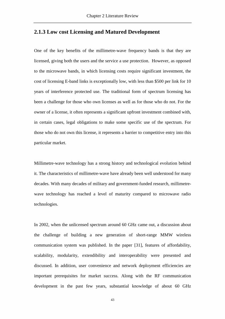
Chapter 2 Literature Review
43
2.1.3 Low cost Licensing and Matured Development
One of the key benefits of the millimetre-wave frequency bands is that they are
licensed, giving both the users and the service a use protection. However, as opposed
to the microwave bands, in which licensing costs require significant investment, the
cost of licensing E-band links is exceptionally low, with less than $500 per link for 10
years of interference protected use. The traditional form of spectrum licensing has
been a challenge for those who own licenses as well as for those who do not. For the
owner of a license, it often represents a significant upfront investment combined with,
in certain cases, legal obligations to make some specific use of the spectrum. For
those who do not own this license, it represents a barrier to competitive entry into this
particular market.
Millimetre-wave technology has a strong history and technological evolution behind
it. The characteristics of millimetre-wave have already been well understood for many
decades. With many decades of military and government-funded research, millimetre-
wave technology has reached a level of maturity compared to microwave radio
technologies.
In 2002, when the unlicensed spectrum around 60 GHz came out, a discussion about
the challenge of building a new generation of short-range MMW wireless
communication system was published. In the paper [31], features of affordability,
scalability, modularity, extendibility and interoperability were presented and
discussed. In addition, user convenience and network deployment efficiencies are
important prerequisites for market success. Along with the RF communication
development in the past few years, substantial knowledge of about 60 GHz

Chapter 2 Literature Review
44
millimetre-wave channels has developed. A great deal of work for the commercial use
of millimetre-wave has also been carried out.
2.2 Millimetre-wave Antenna
In the recent decade, with the announcement of unlicensed frequency band,
millimetre-wave antennas have rapidly developed.
As discussed in Chapter 1, one of the attractions of 60 GHz is the high attenuation
along the propagating path. The heavy absorption of atmosphere at 60 GHz spectrum
can reduce the wave propagating diffraction effect and increase the high free space
loss. Therefore, at 60 GHz, the wireless propagating path between the transmitter and
receiver can easily be disturbed. Early in 1996, C. Peixeiro and his colleagues
designed a planar microstrip patch antenna array for the mobile station operating from
62 GHz to 63 GHz [19]. The antenna array was built up on the substrate of RT/Duriod
5880 and had obtained a maximum gain of 10.8 dB. However, the feeding network
presented in this antenna array could radiate energy in the millimetre frequency band,
causing the cross polarisation and side lobe radiation. In order to reduce these effects,
researchers in [32] used the slot-coupled printed antenna array to separate the feeding
network from the ground. As shown in Fig.2-3, a ground plane with slot in the centre
separates the radiating element from feeding line.
The array is finally arranged as illustrated in Fig.2-13, which substantially increased
the antenna radiation performance. This millimetre-wave antenna has the advantage
of low cost, but it is not compatible with other millimetre-wave products.
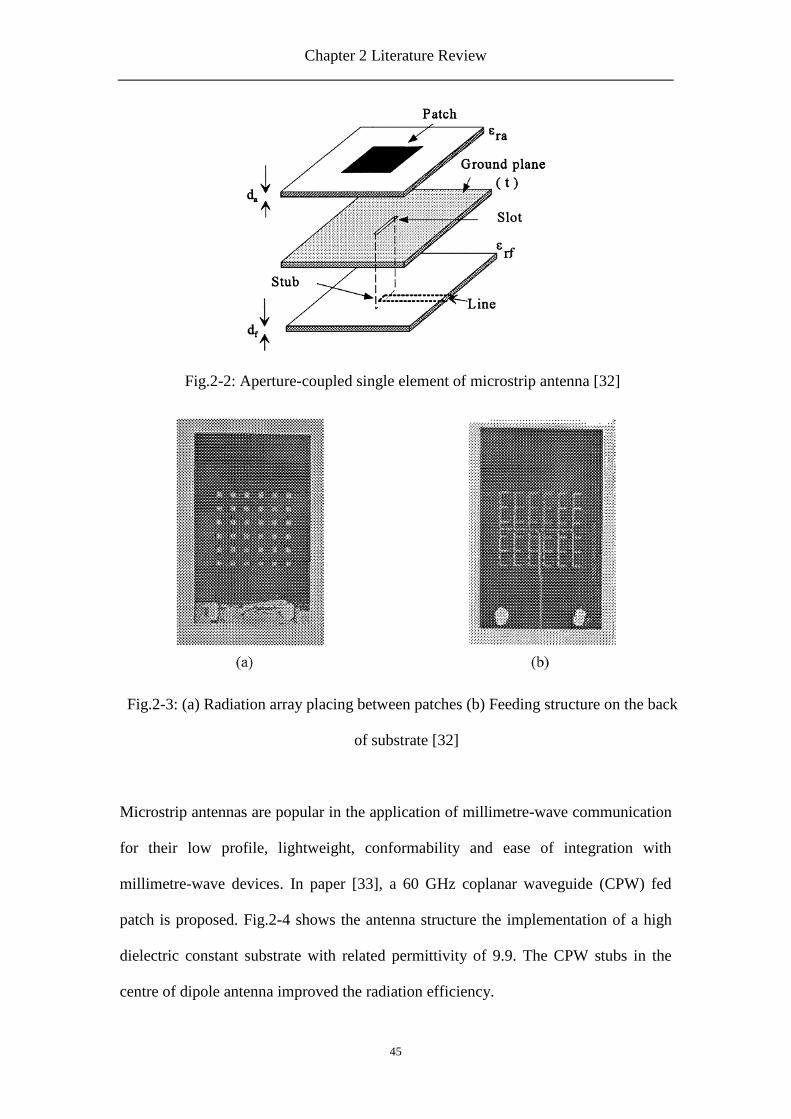
Chapter 2 Literature Review
45
Fig.2-2: Aperture-coupled single element of microstrip antenna [32]
Fig.2-3: (a) Radiation array placing between patches (b) Feeding structure on the back
of substrate [32]
Microstrip antennas are popular in the application of millimetre-wave communication
for their low profile, lightweight, conformability and ease of integration with
millimetre-wave devices. In paper [33], a 60 GHz coplanar waveguide (CPW) fed
patch is proposed. Fig.2-4 shows the antenna structure the implementation of a high
dielectric constant substrate with related permittivity of 9.9. The CPW stubs in the
centre of dipole antenna improved the radiation efficiency.
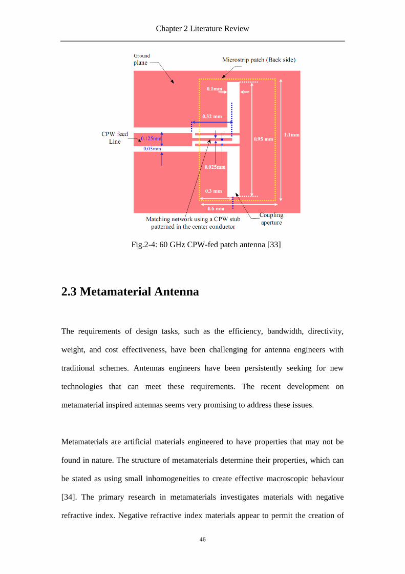
Chapter 2 Literature Review
46
Fig.2-4: 60 GHz CPW-fed patch antenna [33]
2.3 Metamaterial Antenna
The requirements of design tasks, such as the efficiency, bandwidth, directivity,
weight, and cost effectiveness, have been challenging for antenna engineers with
traditional schemes. Antennas engineers have been persistently seeking for new
technologies that can meet these requirements. The recent development on
metamaterial inspired antennas seems very promising to address these issues.
Metamaterials are artificial materials engineered to have properties that may not be
found in nature. The structure of metamaterials determine their properties, which can
be stated as using small inhomogeneities to create effective macroscopic behaviour
[34]. The primary research in metamaterials investigates materials with negative
refractive index. Negative refractive index materials appear to permit the creation of
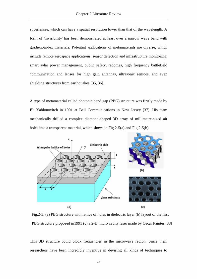
Chapter 2 Literature Review
47
superlenses, which can have a spatial resolution lower than that of the wavelength. A
form of 'invisibility' has been demonstrated at least over a narrow wave band with
gradient-index materials. Potential applications of metamaterials are diverse, which
include remote aerospace applications, sensor detection and infrastructure monitoring,
smart solar power management, public safety, radomes, high frequency battlefield
communication and lenses for high gain antennas, ultrasonic sensors, and even
shielding structures from earthquakes [35, 36].
A type of metamaterial called photonic band gap (PBG) structure was firstly made by
Eli Yablonovitch in 1991 at Bell Communications in New Jersey [37]. His team
mechanically drilled a complex diamond-shaped 3D array of millimetre-sized air
holes into a transparent material, which shows in Fig.2-5(a) and Fig.2-5(b).
Fig.2-5: (a) PBG structure with lattice of holes in dielectric layer (b) layout of the first
PBG structure proposed in1991 (c) a 2-D micro cavity laser made by Oscar Painter [38]
This 3D structure could block frequencies in the microwave region. Since then,
researchers have been incredibly inventive in devising all kinds of techniques to

Chapter 2 Literature Review
48
generate band-gaps at different frequencies in a wide range of materials from silicon
to plastics.
When the PBG structures were applied for electromagnetic wave application, they
were also known as electromagnetic band gap (EBG) structures. Recently, several
authors proposed the application of EBG structures in [39-42] as superstrates in order
to improve the antenna performances. Typically, an EBG array, which consists of
dielectric elements and characterised by stop/pass bands is employed as a cover for
antennas to enhance the gain of a single patch antenna. Frequency selective surface
(FSS) was also been proposed as an alternative to dielectric EBGs for gain
enhancement [43]. The FSS offers similar transmission and reflection characteristics,
but is thinner than the EBG configuration. However, the distance between the FSS
superstrate and the ground plane, which determines the resonant frequency, needs to
be carefully designed.
In recent years, AMCs have attracted much attention from the academic society and
industry. AMC structures are typically formed by periodic patterns based on dielectric
substrates. An AMC structure has a property of high impedance surface (HIS). It was
first reported in Sievenpiper‟s work, which has a forbidden frequency band over
which waves cannot been propagated [44]. Once a suitable AMC structure is applied
to antenna, unwanted ripples at AMC forbidden frequency band can be eliminated.
HIS works within the frequency range, where the tangential magnetic field is tiny,
leaving only large electric field [44]. Most recently, AMC structures have reported to
used for designing low profile high gain planar antennas [45, 46] In addition to AMC

Chapter 2 Literature Review
49
structures, other Metamaterial structures have also demonstrated their benefits for
higher directivity, low profile and planar antennas [47-50].
Fig.2-6: Different types of metamaterial simulating in waveguide [50]
In [50], many types of metamaterail structures were studied. Structures as shown in
Fig.2-6 are several published metamaterial unit element structures that have been used
to enhance the antenna performance.
In [51], The authors show how a flat slab made of a metamaterial engineered to have
a small negative index of refraction can be used to reshape radiation emitted from an
isotropic source and produce a highly directional output beam. In [52], a multilayer
grid structure that can significantly increase the antenna directivity and gain was
extended to millimetre-wave frequencies.

Chapter 2 Literature Review
50
In addition of increase to the directivity and gain, it has also been reported that low
profile antenna radiation characteristics can be improved by using AMC [53-55]. In
[54], a printed electric dipole antenna was intergraded into a volumetric metamaterial-
based AMC block, as shown in Fig.2-7. It was demonstrated numerically in HFSS
that resonant modes could be excited to produce either large front-to-back ratios or
large broadside directivities. The proposed 3D AMC block can be constructed with
only two unit layers of capacitively loaded loop (CLL) elements that are
symmetrically positioned along the x-axis. The printed dipole was designed to be
symmetric both in the x and z directions. The block layers are symmetric about the
printed dipole layer in the z direction. This structure works at 9.45 GHz and obviously,
the structure of AMC is not easy to fabricate.
Fig.2-7: Specifications of the two CLL element deep unit layer and the overall
configuration [54].
Besides CLL multilayer structure, more simple planar AMC structure can be used to
increase low profile antenna efficiency. Researchers in [56] presented characteristics
of microstrip patch antennas on metamaterial substrates loaded with complementary
split-ring resonators (CSRRs). The proposed CSRR structure is placed in the ground

Chapter 2 Literature Review
51
plane of the substrate. Simulation results were verified by experimental results
confirming that the CSRR loaded patch antenna achieves size reduction as well as
bandwidth improvement. Fig.2-8 shows the antenna structure.
Fig.2-8: Configuration of the metamaterial antenna [56].
Metamaterial structure can even be applied to antenna itself, i.e, the antenna itself is
made of metamaterials [57, 58], where patch antenna worked at 7 GHz with
bandwidth enhancement from 200 MHz to 3.2 GHz. The structure is shown in Fig.2-9.
Fig.2-9: Top and side view of the proposed patch antenna [58]

Chapter 2 Literature Review
52
2.4 On-chip Antenna Investigation
The IC is one of the most important developments within the electronics arena. The
history of the integrated circuit shows that the IC developed as a result of the need for
very small electronic assemblies. Engineers and scientists saw the possibilities of
much greater levels of miniaturisation. IC came out for the need of improving military
equipment. The Second World War had conclusively proved the value of electronics
beyond all doubt. In conventional wireless or radar systems, antenna and circuit are
separated to the subsystem. A circuit antenna module was used to be the interference.
MMIC is a type of IC device that operates at microwave frequencies. MMIC typically
perform functions such as microwave mixing, power amplification, low noise
amplification, and high frequency switching. As both inputs and outputs on MMIC
devices are matched to a characteristic impedance of 50 ohms, MMIC is easier to be
used without an external matching network interference. MMICs were originally
fabricated using compound semiconductor, such as GaAs, InP and SiGe. These
materials have properties of high propagating speed but high costly [4-7, 59].
The exploration of alternative semiconductor technologies demonstrated the first
experimental millimetre-wave transmitter and receiver chips using a high-speed alloy
of SiGe by IBM engineers [8-10].
The primary advantage of Si technology is its lower fabrication cost compared with
GaAs, InP and SiGe. Although silicon wafer diameters are typically 8 inch or 12 inch,
which is larger compared with 4 inch or 6 inch for GaAs, the total costs are lower,

Chapter 2 Literature Review
53
contributing to a less expensive IC. With the efficient and identical fabrication
process as standard Si CMOS, devices such as RF Front-end circuit can be massly
produced. Since the IEEE 802.15.3C Task Group has been formed to standardise
millimetre-wave radios, consumer requirements push the millimetre-wave developing
towards low-cost and high-integrated property. In order to lower the price, the use of
silicon technology to build 60 GHz transceiver components is a good alternative.
From copper oxide to germanium and silicon, the materials were systematically
studied in the 1940s and 1950s. The mainstay in analog and digital mixed
implementation technology is CMOS. Nowadays CMOS technology is widely used
because it provides density and power saving on digital side and also provides a good
combination of components for analogy design. Today, silicon monocrystals are the
main substrate used for ICs to integrate the transceiver and antenna with the digital
signal process blocks using Si CMOS technology [27, 60, 61]. Here in Fig.2-10
illustrates the layout of different sizes of silicon wafers.
The main challenge, however, of building antenna on the Si CMOS substrate is the
substrate loss. A standard Si CMOS substrate has low resistivity (typically ~10
Ω·cm) and high permittivity, which dissipates electromagnetic power, hence
significantly decreases the antenna radiation efficiency.

Chapter 2 Literature Review
54
Fig.2-10: Silicon wafer from IBM in different sizes [62].
The plot in Fig.2-11 shows two S-parameters, S11 and S21 of a 1 mm microstrip
transmission line based on silicon substrate [63]. As silicon has low resistivity, the
reflection coefficient from 0 to 100 GHz remains lower than -10 dB and the
transmission coefficient stays below -3 dB. Fig.2-12 shows the S-parameter result of a
substrate with 1000 Ω·cm resistivity substrate. It can be easily concluded that the
energy loss is due to the low resistivity property of the silicon.
Fig.2-11: S-parameter plot of transmission line with standard silicon substrate [63]

Chapter 2 Literature Review
55
Fig.2-12: S-parameter plot of transmission line with 1000 Ω·cm resistivity substrate [63]
Several antennas built on different type of silicon substrates have been reported. For
instance, in 2007, a quasi-yagi antenna operating at 100 GHz with silicon integrating
technology was reported.
Fig.2-13: (a) top view layout (b) cross-sectional view illustration [26]
Fig.2-13 shows the structure of quasi-Yagi antenna from top and cross-sectional
views. This antenna consists of one driver, two directors and a truncated ground plane

Chapter 2 Literature Review
56
which acts as a reflector. It is fed by a uniplanar broadband microstrip-to-coplanar
strip transition etching on the top aluminium layer and is shown in Fig.2-13(a). As the
cross-sectional layout shows Fig.2-13(b), main the antenna is formed by two 2 μm
aluminium layers separating by a 2 μm thick SiO2 layer. Besides the feeding structure,
directors and driver are etched on the top aluminium layer while the reflector is
etched on the bottom layer.
Yagi-uda antenna is famous for its high directivity so this quasi-yagi antenna was
fabricated on silicon substrates for low resistivity 10 Ω·cm using the post back end of
line (post-BEOL) process. Post-BEOL processing indicates Beck End of line. It is a
fabrication for transistors, capacitors and resistors. It‟s a package get interconnected
with wafer. As a result, this antenna obtained a bandwidth from 89 GHz to 104 GHz,
8.2 dB return loss and 5.7 dB antenna gain at 100 GHz. However, the dielectric layer
used in this design is 20 m, which is not compatible with any standard Si CMOS
technologies.
In order to reduce the silicon substrate loss, the micromachining technique and proton
implantation process are applied to Si CMOS process [64, 65]. For example in 2007,
D. Liu and his colleagues presented a Si-based packing technology to enlarge the
bandwidth of millimetre-wave system [21]. Fig.2-14 illustrates the layout of antenna
proposed in [21]. The silicon substrate of antenna was implanted to a high resistivity
of 1000 Ω·cm. The antenna is fabricated using a 1.2 μm Cu damascene process. The
cavity is 400 μm deep and metallized with an 8 μm thick Cu layer. However, the
technology is again not compatible with any standard Si CMOS technologies

Chapter 2 Literature Review
57
Fig.2-14: Photograph of antenna (left) and cavity (right) [21].
To design the antenna with standard on-chip technology, the main challenge is that
they are not efficient due to the low resistivity silicon [27, 66, 67] substrate. Most
recently there are some progresses on Si CMOS on-chip antennas. For instance, a new
dipole antenna was presented and obtained a large bandwidth covering from 57 GHz
to 64GHz allocated free band [68], In this paper, a 60 GHz antenna was produced by
130 nm Si CMOS process. A -10 dB matching bandwidth of 11% was also revealed.
The total simulated efficiency was found to be 3%. Fig.2-15 shows the dipole antenna
and substrate layers of 130 nm Si CMOS technology [68].
Fig.2-15: (a) Designed 60 GHz dipole antenna (b) Substrate layers of 130 nm Si
CMOS technology [68]
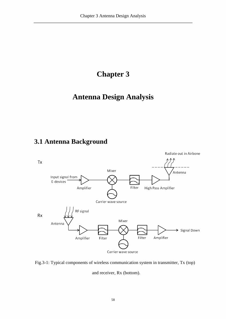
Chapter 3 Antenna Design Analysis
58
Chapter 3
Antenna Design Analysis
3.1 Antenna Background
Fig.3-1: Typical components of wireless communication system in transmitter, Tx (top)
and receiver, Rx (bottom).

Chapter 3 Antenna Design Analysis
59
Antenna is an electrical device, which converts electrical currents into radio waves,
and vice versa. It is usually applied with a radio transmitter or receiver as shown in
Fig.3-1. In the wireless transmission system, analogy signal generated by carrier wave
source is used to carry digital information and it is converted into radio wave to
radiate out into free space through antenna. As Fig.3-1 shows, the input signal flows
into transmit device Tx and mixes with an analogy signal as a carrier, after running
through filter and a high pass amplifier, signal propagates into the antenna and
radiates out in to free space. On the receiver, Rx, RF signal is detected by the antenna
and converted into subsystem by decoding. This is the typical way how the digital
signal is transmitted in a wireless system. In this system, the components and devices
can be classified into active and passive parts. Devices such as amplifiers with power
supply required are defined as active components while others are passive
components. Insertion loss is generated when the power running through the passive
devices. Besides insertion loss, this system has other factors affecting the signal
transmission quality.
The skin effect caused by the changing of magnetic field on the metal surface;
The absorption of RF signal, which is produced by the air;
The reflection, which takes place along the transmission path. If the RF signal
is blocked by any solid objects, reflection appears, the signal propagation path
changes its direction;
Matching is important for a circuit in the system. It makes power radiation
efficiently. VSWR is a way to measure how system matches and give a value
of 1 at perfect match. Besides that, the reflection coefficient of S-parameter is
another way to observe matching situation.

Chapter 3 Antenna Design Analysis
60
3.2 Antenna Parameters
Antenna is the interface between the device and RF wave transmission environment.
The main function of antenna is either sending or receiving RF energy between the
circuit and free space. The antenna changes electrical current into airborne wave which
radiates out into space. Fundamentally, any metallic objects about the size of their
wavelength works as an antenna to radiate RF energy. Radiation is generated by the
varying of velocity of charges such as speed, direction and oscillation. There are
mainly four parameters describing the performance of an antenna. In this section,
parameters are studied and their relationships with radiation will also be presented.
3.2.1 Radiation Power Density
Radiation power density shows an average power radiating out from an antenna. It
can be estimated by integrating power surrounded the antenna. However the equation
is based on another concept, which is radiation intensity. Radiation intensity in a
given direction has specified the power radiated from an antenna per unit solid angle.
Solid angle is a sphere angle with its vertex at the centre of a sphere of radius r, which
refers to a steradian. Since it is a far-field parameter, the equation can be expressed as
follows:
𝑈 = 𝑟2𝜔𝑟𝑎𝑑 (2)
where 𝑟 is radius of sphere and 𝜔𝑟𝑎𝑑 is the radian of solid angle.
The radiation power density can be obtained as
(3) SS S
avradavrad dsHEdandsPP )Re(2
1ˆ *

Chapter 3 Antenna Design Analysis
61
The radiation power density takes the average power of the integration power within
an infinitesimal area of closed surface. E and H are the electric and magnetic field
generating in the radiation area, 𝜔𝑟𝑎𝑑 is the radian of solid angle and 𝜔𝑎𝑣 is the radian
of an average angle. Real part of /2 represents the average power density.
3.2.2 Power Gain and Directivity
The power gain and directivity are parameters that define the ability of antenna
concentrating power in particular direction. It may be regarded as the ability of the
antenna to direct radiated power in a given direction. This is an inherent property of
the antenna that only includes the ohmic or dissipative losses arising from
conductivity of metal and dielectric loss. As an antenna radiates power in sphere, 3D
radiation pattern can be divided by two perpendicular planes, which are elevation and
azimuth plane. Details of radiation pattern will be presented in Section 3.2.5.
However, the power gain can be measured in a specified direction (𝜃, 𝜙), where 𝜃 is
the scanning angle in elevation plane and 𝜙 is that angle in azimuth plane.
𝐺 𝜃, 𝜙 = 4𝜋× 𝑝𝑜𝑤𝑒𝑟 𝑟𝑎𝑑𝑖𝑎𝑡𝑒𝑑 𝑝𝑒𝑟 𝑢𝑛𝑖𝑡 𝑠𝑜𝑙𝑖𝑑 𝑎𝑛𝑔𝑙𝑒 𝑖𝑛 𝑑𝑖𝑟𝑒𝑐𝑡𝑖𝑜𝑛 (𝜃 ,𝜙)
𝑇𝑜𝑡𝑎𝑙 𝑝𝑜𝑤𝑒𝑟 𝑎𝑐𝑐𝑒𝑝𝑡𝑒𝑑 𝑓𝑟𝑜𝑚 𝑠𝑜𝑢𝑟𝑐𝑒 (4)
Similar to the power gain expression, directivity, D indicates the ability of the
directional antenna propagate power to a required direction. Nevertheless, different
from gain, directivity does not count in the dissipative losses. It is a ratio of radiation
intensity in a given direction to the average radiation intensity. Directivity, 𝐷 𝜃, 𝜙
can be calculated through an equation
)( *HE
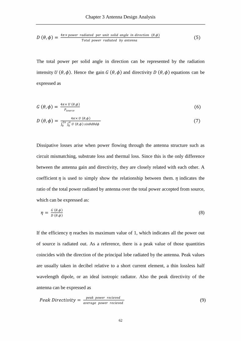
Chapter 3 Antenna Design Analysis
62
𝐷 𝜃, 𝜙 = 4𝜋× 𝑝𝑜𝑤𝑒𝑟 𝑟𝑎𝑑𝑖𝑎𝑡𝑒𝑑 𝑝𝑒𝑟 𝑢𝑛𝑖𝑡 𝑠𝑜𝑙𝑖𝑑 𝑎𝑛𝑔𝑙𝑒 𝑖𝑛 𝑑𝑖𝑟𝑒𝑐𝑡𝑖𝑜𝑛 (𝜃 ,𝜙)
𝑇𝑜𝑡𝑎𝑙 𝑝𝑜𝑤𝑒𝑟 𝑟𝑎𝑑𝑖𝑎𝑡𝑒𝑑 𝑏𝑦 𝑎𝑛𝑡𝑒𝑛𝑛𝑎 (5)
The total power per solid angle in direction can be represented by the radiation
intensity 𝑈 𝜃, 𝜙 . Hence the gain 𝐺 𝜃, 𝜙 and directivity 𝐷 𝜃, 𝜙 equations can be
expressed as
𝐺 𝜃, 𝜙 = 4𝜋× 𝑈 𝜃 ,𝜙
𝑃𝑠𝑜𝑢𝑟𝑐𝑒 (6)
𝐷 𝜃, 𝜙 = 4𝜋× 𝑈 𝜃 ,𝜙
𝑈 𝜃 ,𝜙 𝑠𝑖𝑛𝜃𝑑𝜃𝑑𝜙𝜋
02𝜋
0
(7)
Dissipative losses arise when power flowing through the antenna structure such as
circuit mismatching, substrate loss and thermal loss. Since this is the only difference
between the antenna gain and directivity, they are closely related with each other. A
coefficient 𝜂 is used to simply show the relationship between them. 𝜂 indicates the
ratio of the total power radiated by antenna over the total power accepted from source,
which can be expressed as:
𝜂 = 𝐺 𝜃 ,𝜙
𝐷 𝜃 ,𝜙 (8)
If the efficiency 𝜂 reaches its maximum value of 1, which indicates all the power out
of source is radiated out. As a reference, there is a peak value of those quantities
coincides with the direction of the principal lobe radiated by the antenna. Peak values
are usually taken in decibel relative to a short current element, a thin lossless half
wavelength dipole, or an ideal isotropic radiator. Also the peak directivity of the
antenna can be expressed as
𝑃𝑒𝑎𝑘 𝐷𝑖𝑟𝑒𝑐𝑡𝑖𝑣𝑖𝑡𝑦 = 𝑝𝑒𝑎𝑘 𝑝𝑜𝑤𝑒𝑟 𝑟𝑒𝑐𝑖𝑒𝑣𝑒𝑑
𝑎𝑣𝑒𝑟𝑎𝑔𝑒 𝑝𝑜𝑤𝑒𝑟 𝑟𝑒𝑐𝑖𝑒𝑣𝑒𝑑 (9)

Chapter 3 Antenna Design Analysis
63
3.2.3 Radiation Impedance and Efficiency
Impedance is important for the antenna system design, especially for matching.
Antenna is the interface between electromagnetic device and air. In order to reduce
the return loss and improve the radiation efficiency, antenna should be perfectly
matched. Antenna input impedance can be considered to be the sum of self-
impedance and mutual impedance, which can be expressed as:
𝐼𝑛𝑝𝑢𝑡 𝑖𝑚𝑝𝑒𝑑𝑎𝑛𝑐𝑒 = 𝑠𝑒𝑙𝑓 𝑖𝑚𝑝𝑒𝑑𝑎𝑛𝑐𝑒 + 𝑚𝑢𝑡𝑢𝑎𝑙 𝑖𝑚𝑝𝑒𝑑𝑎𝑛𝑐𝑒 (10)
As equation 10 shows, self impedance is the impedance that can be measured at the
input terminals of the antenna and mutual impedance is reactance generate by
influence of coupling to the antenna from other sources. The self-impedance is
consisted of antenna resistance and self-reactance, arising from reactive energy in
near-field region as shown in the following equation:
𝑆𝑒𝑙𝑓 𝑖𝑚𝑝𝑒𝑑𝑎𝑛𝑐𝑒 = (𝑎𝑛𝑡𝑒𝑛𝑛𝑎 𝑟𝑒𝑠𝑖𝑠𝑡𝑎𝑛𝑐𝑒) + 𝑗(𝑠𝑒𝑙𝑓 𝑟𝑒𝑎𝑐𝑡𝑎𝑛𝑐𝑒) (11)
The antenna resistance indicates the sum of radiation resistance Rr and a loss
resistance RL. The sum of Rr and RL refers to the antenna equivalent resistance as
equation 12 shows. It indicates the dissipated power consist radiated power and ohmic
losses.
𝐴𝑛𝑡𝑒𝑛𝑛𝑎 𝑟𝑒𝑠𝑖𝑠𝑡𝑎𝑛𝑐𝑒 = 𝑅𝑟 + 𝑅𝐿 12

Chapter 3 Antenna Design Analysis
64
According to equation 12, radiation efficiency 𝜂 can be defined as
𝜂 = 𝑅𝑟/ (𝑅𝑟 + 𝑅𝐿) 13
Therefore, for an efficient antenna, it is importance to have radiation resistance which
is greater than loss resistance, and the higher the Rr compared with RL, the higher the
efficiency.
3.2.4 Antenna Field Zones
Since electromagnetic field exists surrounding the radiating source and varies with
distance from an antenna, two principle regions located in free-space are defined
according as distance away from the antenna. They are called near field or Fresnel
zone and far field or Fraunhofer zone. Near field is the area close to antenna itself
while far field is distance, R, apart from antenna. Distance, R formed a boundary
between two regions
𝑅 =2𝐿2
𝜆
(14)
where L is the maximum dimension of the antenna and 𝜆 is the wavelength at antenna
resonant frequency. In near field, the power varies with the distance to the antenna.
However, in the far field, all power flow is directed radially outward to infinity and
the shape of field pattern is independent of the distance. Normally far field is a
measurable field which is used to measure antenna parameters such as power gain,
directivity and radiation pattern. Fig.3-2 shows sketch of radiation regions around an
antenna.

Chapter 3 Antenna Design Analysis
65
Fig.3-2: Antenna region, near field and far field.
3.2.5 Radiation Pattern
The mathematical and graphical parameter to represent the magnetic or electric field
around the antenna is called radiation pattern. For an antenna, the term radiation
pattern can be referred to near-field pattern or far-field pattern. The near-field pattern
refers to the positional dependence of the electromagnetic field. The near-field pattern
is commonly obtained by measuring a plane placed in front of the source, or a
cylindrical, or a spherical surface enclosing it. The far-field pattern is measured over
the antenna propagating range where the electromagnetic field does not change with
different positions. Far-field pattern shows a plot of the antenna energy radiation
distribution. This is the pattern that graphically shows a number of important
variables regarding the antenna performance. For example, power flux density,
radiation intensity, directive gain and polarization.
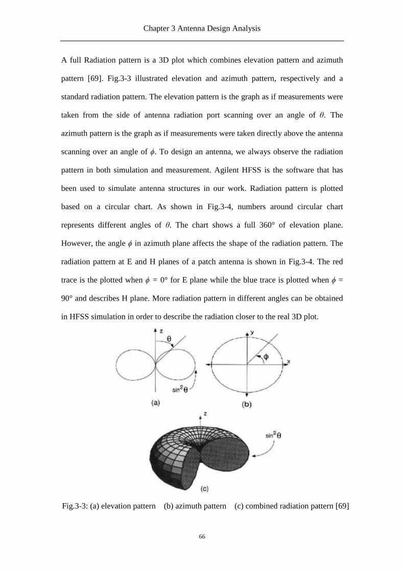
Chapter 3 Antenna Design Analysis
66
A full Radiation pattern is a 3D plot which combines elevation pattern and azimuth
pattern [69]. Fig.3-3 illustrated elevation and azimuth pattern, respectively and a
standard radiation pattern. The elevation pattern is the graph as if measurements were
taken from the side of antenna radiation port scanning over an angle of θ. The
azimuth pattern is the graph as if measurements were taken directly above the antenna
scanning over an angle of ϕ. To design an antenna, we always observe the radiation
pattern in both simulation and measurement. Agilent HFSS is the software that has
been used to simulate antenna structures in our work. Radiation pattern is plotted
based on a circular chart. As shown in Fig.3-4, numbers around circular chart
represents different angles of θ. The chart shows a full 360° of elevation plane.
However, the angle ϕ in azimuth plane affects the shape of the radiation pattern. The
radiation pattern at E and H planes of a patch antenna is shown in Fig.3-4. The red
trace is the plotted when ϕ = 0° for E plane while the blue trace is plotted when ϕ =
90° and describes H plane. More radiation pattern in different angles can be obtained
in HFSS simulation in order to describe the radiation closer to the real 3D plot.
Fig.3-3: (a) elevation pattern (b) azimuth pattern (c) combined radiation pattern [69]

Chapter 3 Antenna Design Analysis
67
Fig.3-4: Radiation pattern in E-H plane
Antennas also can be classified according to their radiation patterns. Isotropic antenna,
which has an ideal point source, radiates the same amount of energy in all spherical
directions. The radiation pattern of isotropic antenna can be seen as a sphere with
antenna centred. Isotropic antenna is an ideal point antenna and this is only the
theoretical case. Normally isotropic antenna is used as a reference radiator. In fact, a
similar spherical radiation pattern can be generated from omni-directional antennas.
They radiate and receive energy equally in all directions around themselves. Since
radiation signal has the same strength within a sphere area around source, this type of
antenna can be used to broadcasting a signal to all points. Fig.3-5(a) shows the plot of
isotropic and omni-directional antenna pattern.
Fig.3-5: (a) isotropic and omni-directional antenna; (b) directional antenna
90 degree
0 degree
Angle θ in
elevation
plane from
-180° to 180°

Chapter 3 Antenna Design Analysis
68
Different radiation formation was applied in directional antenna. Directional antenna
radiates RF energy in a desirable direction, and it also has higher signal strength along
the desirable direction than omni-directional antenna when both of them radiate the
same amount of power. Ideally, directional antenna only has its energy field pattern at
the request sending or receiving directions as Fig.3-5(b) shows. In that plot, taken a
slice of a plane through the 3D pattern, antenna parameters can be measured. For
example, gain can be measured in decibel over either a dipole or a theoretical
isotropic radiator, which is normally called antenna power gain or directional gain.
In a directional antenna pattern, energy field presents as lobes around the source.
There is a main beam for directional antenna, which contains most power flowing out
from the antenna source. At the same time, not all the power can be leading to the
same required direction. A part of power transmits to other directions with an angle or
even backward. These existing lobes are called side lobe and back lobe. Fig.3-6
illustrates a sketch of directional radiation pattern detailed with some determined
variables and parameters as an example.
As shown in Fig.3-6, a main beam with maximum energy of 0 dB, two -20 dB side
lobes and some back lobes can be seen in this directional antenna radiation pattern.
Combining the structure with a normalized relative signal strength margin plane, half
power beam width (HPBW) and beam width between first nulls beam width (FNBW)
can be obtained from Fig.3-6. HPBW refers to the angel where the radiated power
strength reaches half of total radiation power. FNBW refers to the angle between two
nulls from each side of the main radiation beam.

Chapter 3 Antenna Design Analysis
69
Fig.3-6: Radiation pattern with main beam and side lobes in normalized relative signal
strength [70]
3.2.6 VSWR Parameter
Voltage standing wave ratio (VSWR) is the parameter that can estimate the
bandwidth and the quality of antenna impedance match. In the case of the microstrip
antenna, it is usually the impedance, rather than the pattern which affects the
bandwidth of the antenna. Range of frequencies within which the value of VSWR is
less than certain value, S is defined as the bandwidth of the antenna. The bandwidth of
the antenna is related to the total quality factor as:
(15)
where is the total quality factor and in some applications the value of S is taken as
2, which corresponds to a return loss of 9.5 dB or 11% reflected power.
100( 1)( ) %
T
SBandwidth BW
Q S
TQ

Chapter 3 Antenna Design Analysis
70
Most commercial antennas, however, are specified to be 1.5 : 1 or less over some
bandwidth. Based on a 100 watt radio, a 1.5 : 1 VSWR equates to a forward power of
96 watts and a reflected power of 4 watts, or the reflected power is 4.2% of the
forward power.
3.2.7 Polarization
Polarization is a parameter of an electromagnetic wave propagating direction at
resonant frequency. It indicates the shape and orientation of the locus of the field
extremities vectors as a function of time. With this parameter, transmitting antenna
and receiving antenna can match the mode of polarization to superposition and
enlarge the propagating power. Generally polarization can be divided into linear and
circular two types. Besides these two types, cross polarization is radiation orthogonal
to the desired polarization. For instance, the cross polarization of a vertically
polarized antenna is the horizontally polarized fields. It is unwanted polarization,
which is generated by feeding network.
Fig.3-7: Linear polarization of antenna [71]

Chapter 3 Antenna Design Analysis
71
Fig.3-8: Right hand circular polarization of antenna [71]
The linear polarizations that show in Fig.3-7 consist of vertical, horizontal and
oblique planes while circular types that show in Fig.3-8 include Circular Right Hand,
Circular Left Hand, Elliptical Right Hand and Elliptical Left Hand [71].
3.2.8 Antenna Bandwidth
Antenna Bandwidth indicates the range of frequencies within which the antenna
operates. There are two methods of expressing the relative bandwidth for narrowband
and wideband antenna, respectively.
For narrowband antennas, percentage bandwidth is used to define their narrow
bandwidth. It is expressed as,
𝐵𝑎𝑛𝑑𝑤𝑖𝑑𝑡 =𝑓𝐻−𝑓𝐿
𝑓𝑐= 2
𝑓𝐻−𝑓𝐿
𝑓𝐻+𝑓𝐿 (16)
where 𝑓𝐻 , 𝑓𝐿 are the higher and lower frequency where half power is radiated out,
respectively. 𝑓𝑐 is the centre frequency. Equation 16 shows that the bandwidth is the

Chapter 3 Antenna Design Analysis
72
percentage of the frequency difference over the centre frequency. It is theoretical limit
to 200%, which occurs when 𝑓𝐿 = 0
For wideband antennas, fractional bandwidth is used. The wideband antenna
bandwidth is expressed as the ratio of high frequency to low frequency,
𝐵𝑎𝑛𝑑𝑤𝑖𝑑𝑡𝑓𝑟𝑎 =𝑓𝐻
𝑓𝐿 . (17)
and it is usually presented in form of B : 1, where B is the value of 𝐵𝑎𝑛𝑑𝑤𝑖𝑑𝑡𝑓𝑟𝑎 .
There are many methods dealing with the antenna bandwidth enhancement. Take the
microstrip antenna as an example; the bandwidth can be increased by applying either
a very low dielectric constant substrate or a relatively thick dielectric layer on the
antenna [72]. A superstrate planar can be used for wider the bandwidth [73]. Resonant
cavity can be employed to improve antenna performance [74]. AMC has also been
used to widen microstrip antenna bandwidth [58, 75].
3.3 Antenna Types
The history of antenna design was dated back to the late 19th
century when the first
radio experiments were proposed based on classical electromagnetic field theory [76].
Since then, many different types of antennas have been studied and designed to meet
different needs for both military and commercial use. Nowadays, antennas can be
very broadly classified either by the frequency spectrum in which they are commonly
applied or the structure appearance or based on the mode of radiation. Here we
classified antennas based on their different applications therefore they can be divided
into four categories. Each antenna structures are grouped as listed in Table 3-1.

Chapter 3 Antenna Design Analysis
73
Table 3-1: Classification of antenna
Antenna Types Structures
Wire Dipole; monoploe Loop Yagi-Uda
Aperture Horn
Reflector
Lens
Open-ended waveguide
Planar Microstrip Dipole Slot
Array Aperture Yagi-Uda Patch
Wire antennas including dipoles, monopoles, loops, Yagi-Uda and other similar
structures, they are widely used at lower frequencies from high frequency (HF) up to
ultra-high frequency (UHF) in buildings, cars, aircrafts, ships and etc. Wire antennas
generally have advantage of lightweight, low cost and simple design, while the
radiation gains generated from them are low.
Aperture antennas such as horns, lens, reflectors and open-end waveguides are
normally applied in microwave and millimetre-wave frequencies. They have
moderate to high radiation gain and mainly used in aircraft or spaceship, since they
can be very conveniently flush-mounted in the skin of those aircrafts.
Planar antennas including microstrip patch antennas, planar dipoles and planar slots
are also used in microwave and millimetre-wave frequencies. Planar antennas can be
made with photolithographic methods, such as, printed circuit board (PCB) and Si
CMOS technologies. Planar antennas are also easily arrayed for high gain purpose.
Antenna array consists of a regular arrangement of antenna elements with a feed
network. Antenna elements need to be regular and easy to arrange, such as planar
antennas. The main function of antenna array is controlling the pattern characteristics
such as beam pointing angle and sidelobe levels by adjusting the amplitude and phase
distribution of the array elements.

Chapter 3 Antenna Design Analysis
74
For a 60 GHz wireless network, it is highly desirable to have the antenna embedded in
the chip. Therefore, in this research project, planar antenna will be the choice. In the
following sections, two kinds of planar antennas and a dipole antenna will be
discussed in details.
3.3.1 Microstrip Patch Antenna
Microstrip antennas are often chosen to be applied in millimetre-wave wireless
communications due to their properties of small size, lightweight, low cost and easy
to install. Microstrip antennas are typically formed by etching the metal antenna
element pattern to an insulating dielectric substrate with a metal plane attached to the
bottom of the substrate that functions as a ground plane.
The basic microstrip antenna is the patch antenna. Radiation part of a patch antenna
has many shapes such as square, rectangular, circular and elliptical. There are many
methods to feed patch antennas by using microstrip line, coaxial probe, aperture
coupling and proximity coupling.
Fig.3-9: Structure of patch antenna with microstrip feed

Chapter 3 Antenna Design Analysis
75
Take rectangular patch antenna that shows in Fig.3-9 as an example; it is fed by a
microstrip line. The antenna itself has the main structure of a half-wavelength shaped
metal patched on a dielectric substrate with a relative permittivity, εr. This rectangular
patch is usually designed to operate near the resonant frequency. At resonant
frequency, the imaginary part of the impedance is zero. When signal feeds into the
patch element, a fringing field was produced due to the edge effect of the metal patch.
However, the fringing field acts as an additional length to the patch. Therefore, when
the length of the patch is slightly less than a half wavelength of RF signal propagating
the dielectric substrate media, this device will become a radiative microstrip antenna.
Since the value of length depends on the substrate media as well as the height and
width of the patch then an approximation formula to get the resonant length and it is
shown as:
(18)
where is the free-space wavelength, d is the wavelength in the dielectric, and r is
the substrate dielectric constant.
Electric field distribution was plotted out to represent the fringing field around the
patch and it is shown in Fig.3-10. As shown in the top view of the patch, its radiation
can be represented by two slots, separated by a transmission line of length L and open
circuited at both ends. Along the length of the patch, there are maximum voltage and
minimum current because two ends of the patch can be considered as open circuits.
The fields at edges can be resolved into normal and tangential components with
r
dL
49.049.0

Chapter 3 Antenna Design Analysis
76
respect to the ground plane, which is shown in the patch antenna cross-section in
Fig.3-10.
Top View
Cross-section view
Fig.3-10: Top view and cross-section of patch antenna with electric field around it.
Seeing by the cross-section, the electric field along the edges of the patch has
different direction but with the same magnitude. Since two edges that are separated by
the length L is half-wavelength apart then this can be considered as 180 degree out of
phase. Therefore the total fringing field along length L is null. Seeing from top,
electric fields at two edges are in phase with the same magnitude values. Hence the
maximum radiation field pattern is normal to the surface of the patch antenna.

Chapter 3 Antenna Design Analysis
77
These antennas have the advantages of low profile with conformability for planar and
non-planar surfaces, low-cost fabrication, ease of integration using modern printed-
circuit technology and compatible with MMIC designs. Bandwidth of the patch
antenna itself can be expressed as 𝐵. 𝑊. ∝ 𝜀𝑟−1
𝜀𝑟2
𝑤
𝐿, where w and L are the width
and length of patch, h is the substrate height[77]. According to this equation, height of
the substrate controls the bandwidth value. Therefore bandwidth will decrease as the
substrate thickness decreases. As the consequences planar microstrip patch antenna
provides narrow bandwidth for the thin substrate at millimetre-wave frequency range.
When the patch antenna is fabricated on a relatively thin substrate, it typically has
only approximately 5% bandwidth with respect to the centre frequency. According to
the requirement of high data transmit rate, simple patch antenna cannot meet the
needs.
Many techniques have been used to increase the bandwidth of microstrip patch
antenna, such as using a thicker substrate with lower relative permittivity, or by using
a T-shape feed probe.
3.3.2 Slot Antenna
Slot antenna is widely used in microwave and millimetre-wave communication
systems for its feature of omni-direction. It radiates power around azimuth with
horizontal polarization. In Fig.3-11 a waveguide slot antennas operating from 2 GHz
to 24 GHz is shows with its structure of series slots aligned together.
Fig.3-11: waveguide slot antenna working from 2 to 24 GHz [78]
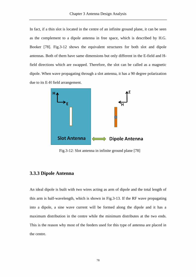
Chapter 3 Antenna Design Analysis
78
In fact, if a thin slot is located in the centre of an infinite ground plane, it can be seen
as the complement to a dipole antenna in free space, which is described by H.G.
Booker [78]. Fig.3-12 shows the equivalent structures for both slot and dipole
antennas. Both of them have same dimensions but only different in the E-field and H-
field directions which are swapped. Therefore, the slot can be called as a magnetic
dipole. When wave propagating through a slot antenna, it has a 90 degree polarization
due to its E-H field arrangement.
Fig.3-12: Slot antenna in infinite ground plane [78]
3.3.3 Dipole Antenna
An ideal dipole is built with two wires acting as arm of dipole and the total length of
this arm is half-wavelength, which is shown in Fig.3-13. If the RF wave propagating
into a dipole, a sine wave current will be formed along the dipole and it has a
maximum distribution in the centre while the minimum distributes at the two ends.
This is the reason why most of the feeders used for this type of antenna are placed in
the centre.
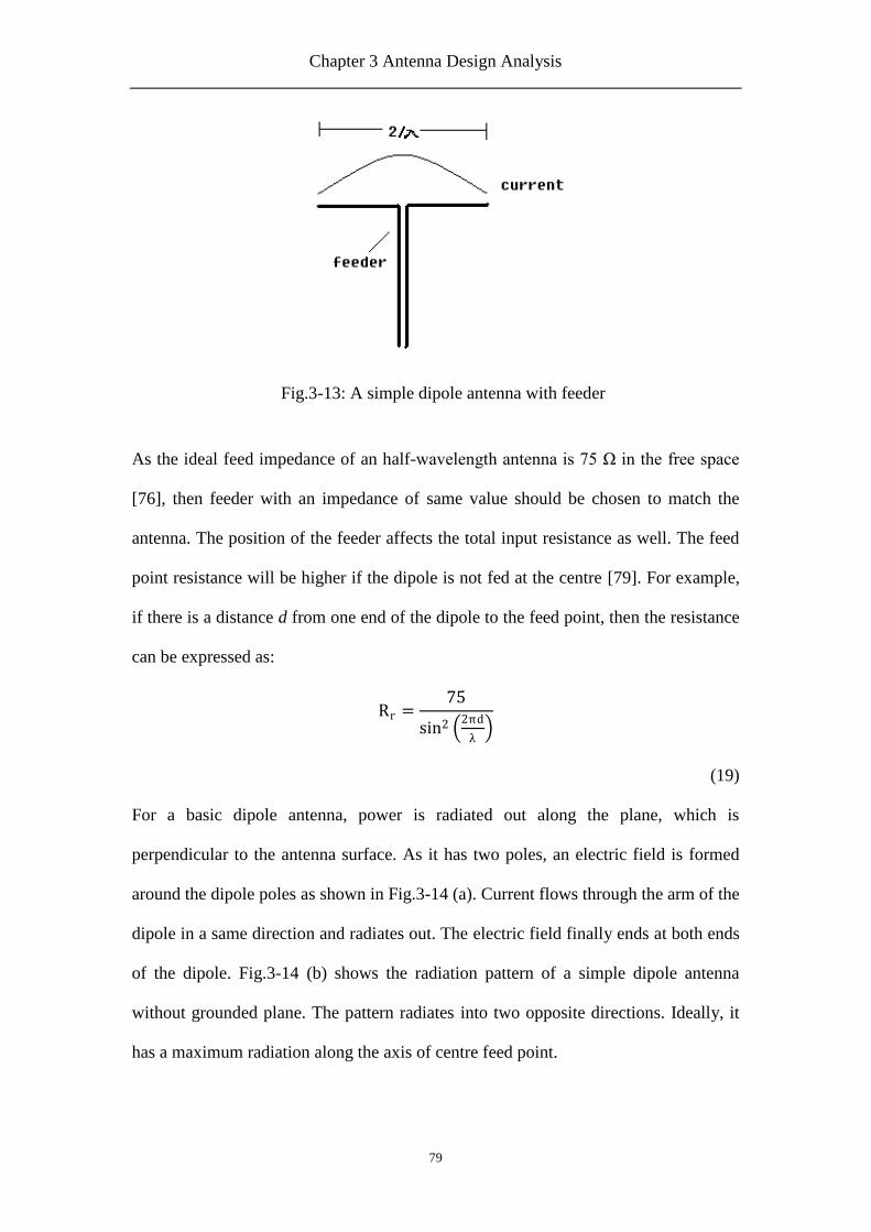
Chapter 3 Antenna Design Analysis
79
Fig.3-13: A simple dipole antenna with feeder
As the ideal feed impedance of an half-wavelength antenna is 75 Ω in the free space
[76], then feeder with an impedance of same value should be chosen to match the
antenna. The position of the feeder affects the total input resistance as well. The feed
point resistance will be higher if the dipole is not fed at the centre [79]. For example,
if there is a distance d from one end of the dipole to the feed point, then the resistance
can be expressed as:
Rr =75
sin2 2πd
λ
(19)
For a basic dipole antenna, power is radiated out along the plane, which is
perpendicular to the antenna surface. As it has two poles, an electric field is formed
around the dipole poles as shown in Fig.3-14 (a). Current flows through the arm of the
dipole in a same direction and radiates out. The electric field finally ends at both ends
of the dipole. Fig.3-14 (b) shows the radiation pattern of a simple dipole antenna
without grounded plane. The pattern radiates into two opposite directions. Ideally, it
has a maximum radiation along the axis of centre feed point.

Chapter 3 Antenna Design Analysis
80
Fig.3-14: (a) Sketch of electric field around the dipole
(b) Radiation pattern of the simple dipole
An antenna that is defined with dipole structure should have an electrical length of
half wavelength. However it is not exactly the value of half wavelength or multiple of
that since the exact length is affected by a factor A. The different factor A is given by
the ratio of the antenna length to the thickness of the metal. A plot of their
relationships is displayed in Fig.3-15.
Fig.3-15: Factor A against the wavelength to thickness ratio [79]

Chapter 3 Antenna Design Analysis
81
Since the resonant frequency depends on the physical length of dipole arm, it is easily
chosen for more accurate length based on the equation 20 and factor A as described in
Fig.3-15 [79].
𝑙𝑒𝑛𝑔𝑡 𝑜𝑓 𝑑𝑖𝑝𝑜𝑙𝑒 𝑚𝑒𝑡𝑒𝑟 =150 × 𝐴
𝑟𝑒𝑠𝑜𝑛𝑎𝑛𝑡 𝑓𝑟𝑒𝑞𝑢𝑒𝑛𝑐𝑦 𝑀𝐻𝑧 (20)
3.4 Conclusion
Background and relevant theories of the antenna design are firstly given in the
beginning of this chapter. In this work, planar antenna is the first choice in order to
designing an on-chip antenna that can operate at 60 GHz. As discussed previously in
the chapter, planar antenna can be fabricated using Si CMOS technology and can be
fully integrated with the RF front-end. Mechanism of how planar antenna works has
been presented in Section 3.3.1 to 3.3.3. Microstrip patch antenna is easy to fabricate
but has a narrow bandwidth while slot antenna is also easy to fabricate and it has
feature of wider bandwidth since the slot can be cut out in different shapes for the
aforementioned purpose.
In this work, planar slot antenna has been chosen as main design due to the bandwidth
requirement. More specifically, the U-shaped slot antenna can provide wider
bandwidth. The slot is cut out of a planar patch and it can generate more than one
resonant frequency by changing the dimension of “U”. By mixing multi resonant
frequencies together, bandwidth becomes wider than single slot or patch antenna. This
structure will be discussed in details in Chapter 4. Besides U-shaped slot antenna,
other planar antennas have also been considered and designed and these will be
discussed in Chapter 5 and Chapter 6.

Chapter 4 Wideband Planar Antenna Investigation
82
Chapter 4
Wideband Planar Antenna Investigation
4.1 Background
Planar antenna is widely used in millimetre-wave antenna design. It is easy to design
and fabricate. However, one single planar antenna such as microstrip patch provides a
narrow bandwidth. This antenna should have a bandwidth of at least 3 GHz to support
the transmission of HD data, with efficiency of greater than 70%. There are many
methods to increase the antenna radiation bandwidth, which can be achieved by
decreasing the dielectric constant of the substrate, increasing the thickness of
substrate, adding superstrate planar upon it, adding resonant cavity or changing the
antenna structure with tapped slots.
In this chapter, U-shaped slot antenna was designed, simulated and analysed. This
antenna is based on a microstrip patch with a U-shaped slot added, which enable it to
work on different frequencies. Different parameters of this U-shaped slot antenna
structure will be simulated and optimised. Since resonant frequency depends on the
antenna structure, different frequencies will be arranged together by varying the
antenna structure.

Chapter 4 Wideband Planar Antenna Investigation
83
However, the U-shaped slot antenna structure performance can be degraded due to the
limitation of substrate height because it is easily affected by the ground distance.
Therefore, a folded dipole antenna was introduced. Folded dipole antenna has a wider
bandwidth than normal dipole and it has an arm length of half wavelength. A full
wave simulation of the folded dipole antenna will be presented here.
4.2 U-shaped Slot Antenna Design and Optimisation
A U-shaped slot is developed for its wide bandwidth by creating two or more closely
adjacent resonant frequencies. The U-shaped slot is cut approximately symmetrical in
the centre of the patch. With this structure, the antenna gives a bandwidth of
approximately 40% for VSWR < 2.
Fig.4-1: Simple structure of a U-shaped slot patch antenna element
A U-shaped slot patch antenna is simple, as shown in Fig.4-1. It consists of a U-
shaped slot and a microstrip feeding. Due to the coupling between the slot and
rectangular metal planar, more than one resonant frequencies are generated. It was
found that the U-shaped slot patch antenna can be designed to attain 50% impedance
bandwidth as well as 30-40% gain of bandwidth [80].

Chapter 4 Wideband Planar Antenna Investigation
84
4.2.1 Design of a Wide Bandwidth U-shaped Slot Patch Antenna
(a)
(b)
Fig.4-2: (a) Side view of antenna layout with parameters indicated (b) Top view
structure of the antenna
Fig.4-2 shows the top and side view layout of antenna with parameters that affect its
radiation performance. The side view illustrated in Fig.4-2(a) shows that the U-shaped
antenna structure consists of four layers, namely the silicon layer, ground layer, SiO2
layer and U-shaped slot patch layer locating from bottom to top. Other than the U-

Chapter 4 Wideband Planar Antenna Investigation
85
shaped slot patch layer, each layer has its own varied width, known as Wsub, Wgnd and
m, respectively. In Fig.4-2(b), the area of m×n refers to the silicon layer and
Wsub×Lsub refers to the SiO2 layer size, which are varied by changing Sy and Sx.
Between those two layers is the ground layer. It has a width of Wsub and a length of
Lsub. The gl and gw are the difference between the dimension of ground plane and SiO2
layer. Therefore the ground size can be changed by varying gl and gw. The metal area
formed by U-shaped slot affects the energy absorbsion and radiation as well. Varying
Sw and Sl can change the slot location. By focusing only on the U-shaped slot, three
gap sizes, rectangular metal width and length could all affect the antenna radiation
performance. The effects from these different parameters on energy radiation will be
discussed later in details. The thickness of SiO2 layer is of 40 μm with a relative
permittivity εr of 4 and the silicon layer is of 150 μm with a relative permittivity εr of
11.9. In this structure, a microstrip line was chosen as feeding. Based on the height of
SiO2 layer, the feed length fl was calculated by the microstrip line calculator defined
as 0.681 mm, which made a match of 50 Ω.
4.2.2 Wave Port Determination in HFSS
The structure of U-shaped slot antenna covered by an air-box with full wave radiation
boundary in HFSS Ver.12 is shown in Fig.4-3. Ansoft HFSS assumes that all
structures are completely encased in a conductive shield with no energy propagating
through it by default. Wave ports are defined in HFSS to indicate the area where
energy enters and exits the conductive shield. With those ports, HFSS assumes that
each of them is connected to a semi-infinite long waveguide that has the same cross
section and same electrical materials known as the port. When the wave port is

Chapter 4 Wideband Planar Antenna Investigation
86
defined correctly, there is a perfectly matched condition at the port in simulation
mode and S-parameters are normalized to frequency only dependent impedance. This
is important for the structural design and simulation. Unsuitable wave port size could
cause inconsistent results that affect the accuraciest of the interaction between the
wave ports and characteristic impedance of the structure. Once the wave port is
correctly designed, a uniform cross section with a certain length is formed. Within the
uniform cross section model the signal of non-propagation modes dies off so that the
accuracies could be improved. The wave port for the microstrip line feed shown in
Fig.4-4 always has a shape of rectangular planar with the correct width and height.
Since an electric field is formed at the surface of the wave port as illustrated in Fig.4-
4, the surface size is taken into consideration. If the wave port size is made smaller
than the waveguide, some RF energy that is unable to propagate into the structure
through the waveguide will be reflected. Overly large wave port is undesirable
otherwise it would weaken the electric field on the feeding cross section surface.
However, there is a range of wave port width within which the resonant frequency
remains constant.
Fig.4-3: Building of radiation air-box

Chapter 4 Wideband Planar Antenna Investigation
87
Fig.4-4: Electric field distribution on wave port
To find a suitable wave port size, the effects with various width are investigated. By
changing the relationship between a and fw, with a being the wave port width and fw
being the feed cross section width, simulation is carried out by observing the return
loss S11. With "Solve ports only" in HFSS solution setup setting, results can be
verified to ensure propagation of the right modes. Amongst many port sizes tested,
only three were chosen for full structure simulation.
Fig.4-5 shows the results tested in full wave mode with three different port sizes of
8×fw, 10×fw and 12×fw. Return loss S11 and VSWR plots against frequency were
shown separately in (a) and (b). It was obvious that the size of 10×fw as shown in red
trace gives a best result in terms of return loss or VSWR. Meanwhile, when the width
has a value greater than 15×fw, there was no power radiated. Notably, between the
port width size of 10×fw and 12×fw, resonate frequency resulted in a slight change,
indicating that it is the correct wave port size range.

Chapter 4 Wideband Planar Antenna Investigation
88
(a)
(b)
Fig.4-5: Comparison between different wave port sizes (a) plot of S11 (b) plot of VSWR
Plot sizes of 10×fw, 8×fw and 12×fw are shown in red, blue and green traces respectively.

Chapter 4 Wideband Planar Antenna Investigation
89
4.2.3 High Gain and Directivity Structure
Fig.4-6: (a) Variables (L1, g1, g2, g3) of U-shaped slot antenna;
(b) Dimensions of each variable for an antenna gain of 5.29 dB
The structure of a U-shaped slot patch antenna is expected to be closely associated
with the performance of antenna radiation. Among those variables shown in Fig.4-6,
length L1 and U-shaped slot width g1, g2 and g3 could directly determine the antenna
radiation gain performance.
The structure built on a 40 μm SiO2 substrate shown in in Fig.4-6(b) gives a gain of
5.29 dB, directivity of 7.29 dB and a reflection coefficient below -20 dB. Simulation
was carried out on variables of L1, g1, g2 and g3 with different values, some results
with comparable changes are shown in Table 4-1. It was observed that the length of
L1 can affect the antenna radiation gain. Once the L1 reached 0.2 mm, the gain
dropped to nearly half to that of directivity, meaning that the radiation efficiency is
below 50%. This was due to partial power reflection at input of antenna as indicated
by the reflection coefficient which stayed on -11 dB.
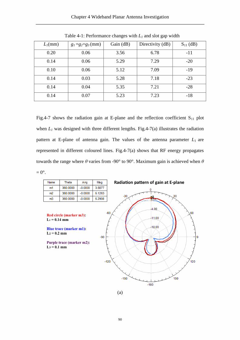
Chapter 4 Wideband Planar Antenna Investigation
90
Table 4-1: Performance changes with L1 and slot gap width
L1(mm) g1 =g2=g3 (mm) Gain (dB) Directivity (dB) S11 (dB)
0.20 0.06 3.56 6.78 -11
0.14 0.06 5.29 7.29 -20
0.10 0.06 5.12 7.09 -19
0.14 0.03 5.28 7.18 -23
0.14 0.04 5.35 7.21 -28
0.14 0.07 5.23 7.23 -18
Fig.4-7 shows the radiation gain at E-plane and the reflection coefficient S11 plot
when L1 was designed with three different lengths. Fig.4-7(a) illustrates the radiation
pattern at E-plane of antenna gain. The values of the antenna parameter L1 are
represented in different coloured lines. Fig.4-7(a) shows that RF energy propagates
towards the range where θ varies from -90° to 90°. Maximum gain is achieved when θ
= 0°.
(a)

Chapter 4 Wideband Planar Antenna Investigation
91
(b)
Fig.4-7: (a) Radiation pattern of gain at E-plane and (b) Reflection coefficient S11 when
L1 = 0.1 mm, 0.14 mm, 0.2 mm
In Fig.4-7(b), the reflection coefficient, S11, when L1 = 0.2 mm, 0.14 mm and 0.1 mm
is shown in blue, red and purple traces, respectively. The results showed that the
highest gain and lowest S11 could be achieved when L1 = 0.14 mm, indicating that the
antenna radiates maximum power out into the directional patch.
Meanwhile, a slight change of gaps in U-shaped slot also affected the radiation results,
as shown in Fig.4-8. Simulations were made when three slots, g1, g2 and g3 have the
width of 0.03 mm, 0.04 mm and 0.07 mm. The radiation pattern of antenna radiation
gain and the reflection coefficient are shown in Fig.4-8(a) and (b), respectively. With
g1 = g2 = g3 = 0.04 mm, the highest gain of 5.35 dB and low reflection coefficient at
two frequencies were achieved.

Chapter 4 Wideband Planar Antenna Investigation
92
(a) Radiation pattern of gain at E-plane
Blue trace: g1 = g2 = g3 = 0.03 mm
Red trace: g1 = g2 = g3 = 0.04 mm
Purple trace: g1 = g2 = g3 = 0.07 mm
(b)
Blue trace: g1 = g2 = g3 = 0.03 mm
Red trace: g1 = g2 = g3 = 0.04 mm
Purple trace: g1 = g2 = g3 = 0.07 mm
Fig.4-8: (a) Gain and (b) S11 plots when g1 = g2 = g3 =0.03 mm, 0.04 mm, 0.07 mm

Chapter 4 Wideband Planar Antenna Investigation
93
Therefore, when the length L1 is approximately 0.14 mm and the U-shaped slot has a
gap width of 0.04 mm, a maximum gain of 5.35 dB with -28 dB reflection coefficient
can be obtained, whereas the bandwidth shown in S11 plot is only 1 GHz with a
resonant frequency at 75.7 GHz.
From Fig.4-8 it was observed that the U-shaped slot antenna worked at three
frequencies at 68 GHz, 75.7 GHz and 94.75 GHz. Radiation patterns in Fig.4-9 and
Fig.4-10 illustrate radiation gain and directivity at the same resonant frequency at
75.7 GHz. Two radiation patterns also show that gain is 5.34 dB, directivity is 7.21
dB and the maximum power gain occurs at the peak of radiation pattern.
Fig.4-9: Radiation pattern of gain when L1 = 0.14 mm and g1 = g2 = g3 = 0.04 mm

Chapter 4 Wideband Planar Antenna Investigation
94
Fig.4-10: Radiation pattern of directivity when L1 = 0.14 mm and g1 = g2 = g3 = 0.04
mm
Fig.4-11: Reflection coefficient plot when L1 = 0.14 mm and g1 = g2 = g3 = 0.04 mm
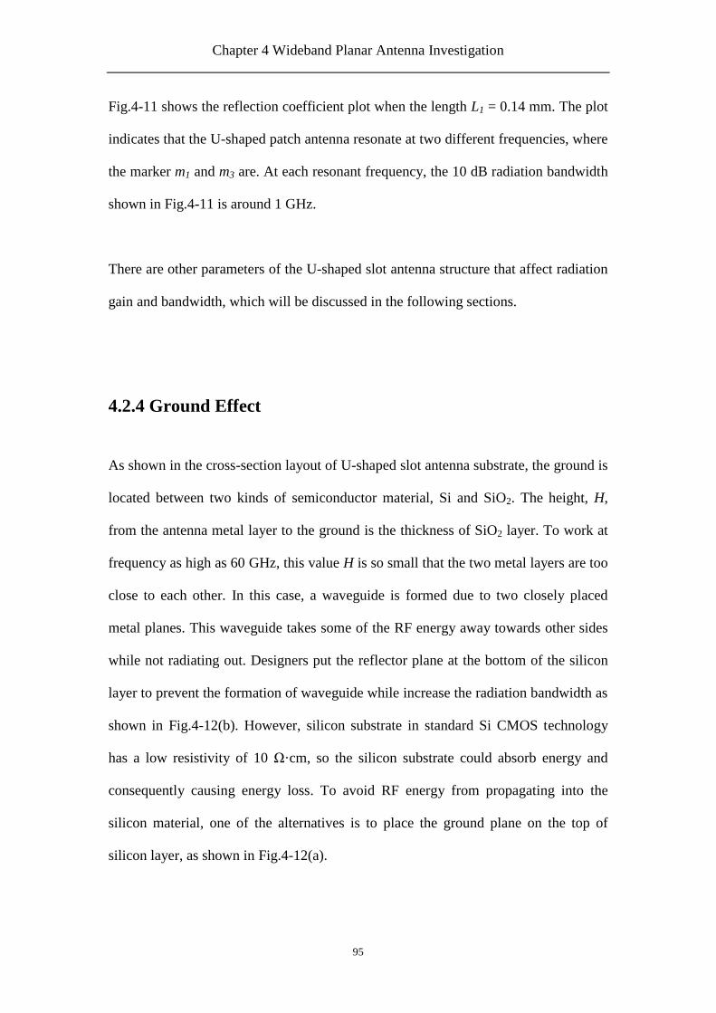
Chapter 4 Wideband Planar Antenna Investigation
95
Fig.4-11 shows the reflection coefficient plot when the length L1 = 0.14 mm. The plot
indicates that the U-shaped patch antenna resonate at two different frequencies, where
the marker m1 and m3 are. At each resonant frequency, the 10 dB radiation bandwidth
shown in Fig.4-11 is around 1 GHz.
There are other parameters of the U-shaped slot antenna structure that affect radiation
gain and bandwidth, which will be discussed in the following sections.
4.2.4 Ground Effect
As shown in the cross-section layout of U-shaped slot antenna substrate, the ground is
located between two kinds of semiconductor material, Si and SiO2. The height, H,
from the antenna metal layer to the ground is the thickness of SiO2 layer. To work at
frequency as high as 60 GHz, this value H is so small that the two metal layers are too
close to each other. In this case, a waveguide is formed due to two closely placed
metal planes. This waveguide takes some of the RF energy away towards other sides
while not radiating out. Designers put the reflector plane at the bottom of the silicon
layer to prevent the formation of waveguide while increase the radiation bandwidth as
shown in Fig.4-12(b). However, silicon substrate in standard Si CMOS technology
has a low resistivity of 10 Ω·cm, so the silicon substrate could absorb energy and
consequently causing energy loss. To avoid RF energy from propagating into the
silicon material, one of the alternatives is to place the ground plane on the top of
silicon layer, as shown in Fig.4-12(a).

Chapter 4 Wideband Planar Antenna Investigation
96
(a) (b)
Fig.4-12: Ground planar location (a) ground plane on top of silicon layer (ground
location in this design) (b) ground plane on the bottom of silicon layer
Another way to decrease the energy loss is by reducing the ground plane size. As
shown in Fig.4-13, when the ground plane gets smaller, RF energy could be stopped
at the edge of the substrate and consequently radiate out due to the edge effect.
Fig.4-13: Ground varying in HFSS structure design
Simulations were taken at two different ground sizes and the results are shown in
Fig.4-14 and Fig.4-15. When the ground size parameters gw = gl = 0 mm, radiation
gain of this antenna is 1.64 dB as shown in Fig.4-14, marker m2. However, a radiation
gain of 2.18 dB is achieved as marker m1 in Fig.4-14 shows, when gw = 0.25 mm and
gl = 0.5 mm.
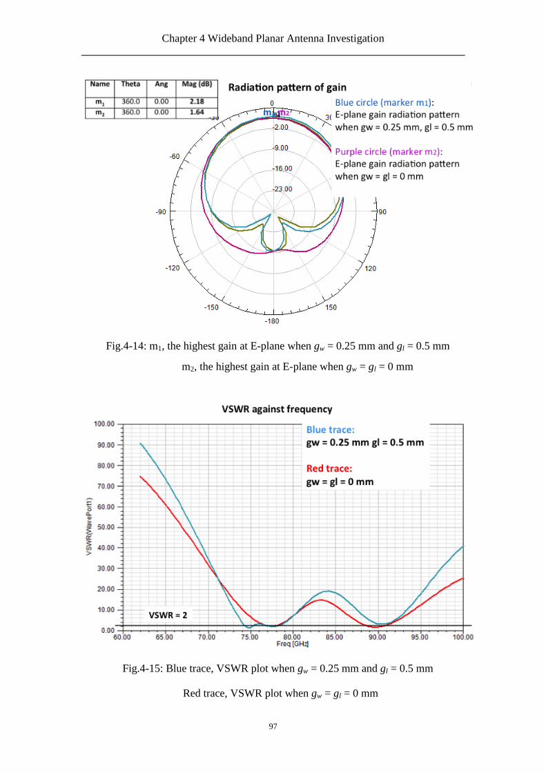
Chapter 4 Wideband Planar Antenna Investigation
97
Fig.4-14: m1, the highest gain at E-plane when gw = 0.25 mm and gl = 0.5 mm
m2, the highest gain at E-plane when gw = gl = 0 mm
Fig.4-15: Blue trace, VSWR plot when gw = 0.25 mm and gl = 0.5 mm
Red trace, VSWR plot when gw = gl = 0 mm

Chapter 4 Wideband Planar Antenna Investigation
98
The ground with gw = 0.25 mm and gl = 0.5 mm gave the gain of 2.18 dB while the
other only has a gain of 1.6 dB. In VSWR plot, blue trace refers to the smaller ground
planar which gives a wider bandwidth than the red one.
4.2.5 Feed Position Effect
Matching is an important element of the design. Only when the circuit is well
matched, the energy can be radiated sufficiently. Impedance matching is a way that is
used in the circuit matching technique. In order to have a successful impedance
matching, the impedance of each part should be calculated or simulated out. To
measure different points along the edge of U-shaped slot, the impedance is different
unless the structure is exactly the same at both sides. However, the reflection
coefficient S11 enables the estimation of the position where the perfect circuit
matching occurs.
Fig.4-16: Reflection coefficient and VSWR varying at three feeding position of -0.25
mm, 0 mm and 0.25 mm

Chapter 4 Wideband Planar Antenna Investigation
99
As shown in Fig.4-16, when the position was at the centre 0 mm (purple trace), it
showed only one resonant frequency at 77 GHz with a reflection coefficient of -6 dB.
At -0.25 mm (red trace), there was another resonant frequency at 90 GHz in addition
to the resonation at 77 GHz. The wide bandwidth at 90 GHz can be used for large
amount of data transfer in wireless communication. With the help of resonant
frequency at 77 GHz, this antenna became a dual-band.
4.2.6 Length of Rectangular Metal
The varying length of rectangular metals mainly change the impedance of the U-
shaped slot, thereby affecting the circuit matching. As shown in Table 4-2, the highest
gain and widest bandwidth is obtained when L1 = 0.05 mm and L2 = 0.09 mm.
Table 4-2: L1, L2 varying effects
L1 (mm) L2 (mm) Gain (dB) Bandwidth (GHz)
0.01 0.09 2.56 4.5
0.05 0.09 2.44 5.5
0.10 0.09 3.17 0.2
0.20 0.09 2.54 0.4
0.05 0.12 1.76 2.0
4.2.7 Rectangular Metal Size
Three blocks of rectangular metals are the main makeup of U-shaped slot structure.
The one in the middle has the main impact on the antenna performance as it couples
with those surrounding slots to radiate energy. Each of the rest two rectangular metals
only has one edge coupling with slots so they don't have much effect to antenna
performance as the middle metal patch.

Chapter 4 Wideband Planar Antenna Investigation
100
According to Fig.4-2, w1, w2 and w3 are three parameters of metal patch width. If they
have the value of 0.58 mm, 0.4 mm and 0.58 mm, respectively, the reflection
coefficient and VSWR are plotted in Fig.4-17, showed three single ripples occuring at
three frequencies separately.
(a)
(b)

Chapter 4 Wideband Planar Antenna Investigation
101
(c)
(d)
Fig.4-17: (a) Reflection coefficient and (b) VSWR when w1 = 0.58 mm, w2 = 0.4 mm,
w3 = 0.58 mm
(c) Reflection coefficient and (d) VSWR when w1 = 0.4 mm, w2 = 0.3 mm, w3 = 0.4 mm
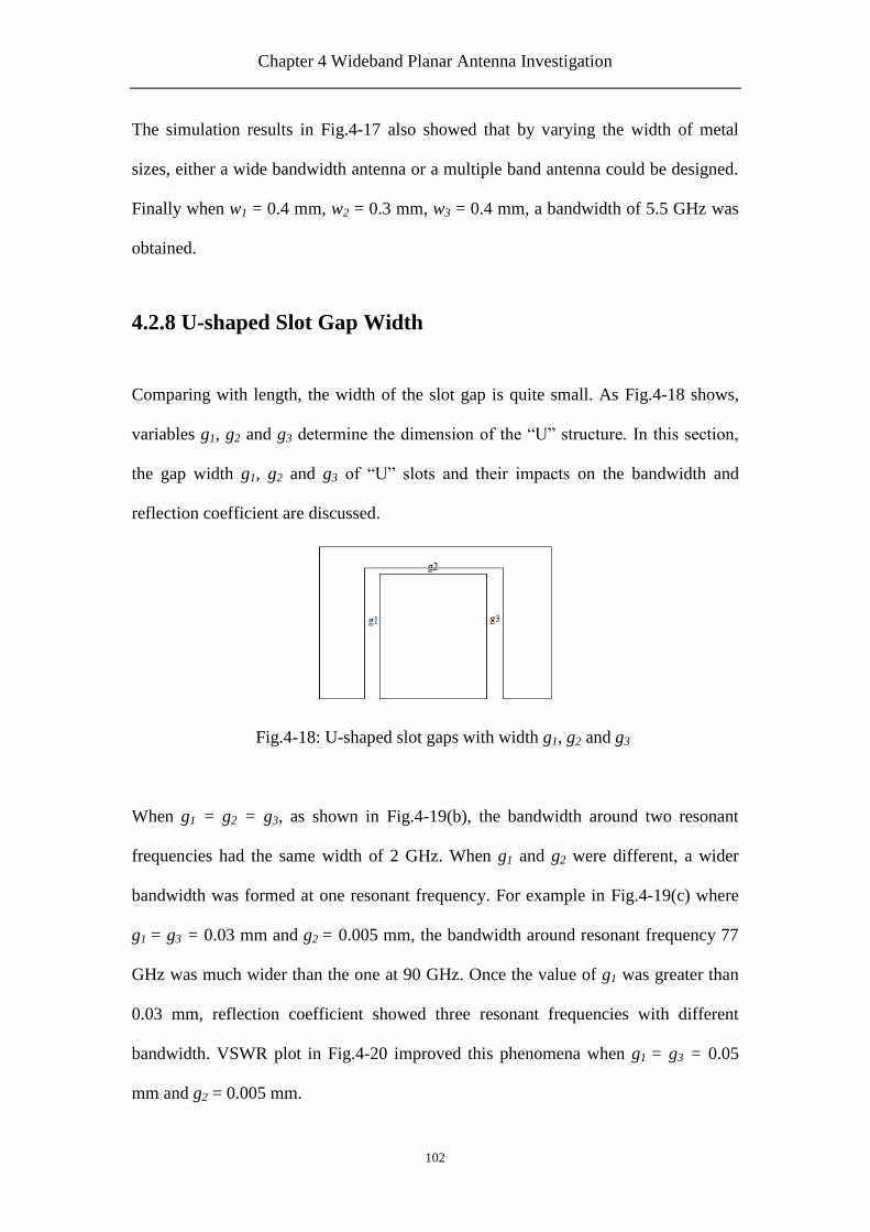
Chapter 4 Wideband Planar Antenna Investigation
102
The simulation results in Fig.4-17 also showed that by varying the width of metal
sizes, either a wide bandwidth antenna or a multiple band antenna could be designed.
Finally when w1 = 0.4 mm, w2 = 0.3 mm, w3 = 0.4 mm, a bandwidth of 5.5 GHz was
obtained.
4.2.8 U-shaped Slot Gap Width
Comparing with length, the width of the slot gap is quite small. As Fig.4-18 shows,
variables g1, g2 and g3 determine the dimension of the “U” structure. In this section,
the gap width g1, g2 and g3 of “U” slots and their impacts on the bandwidth and
reflection coefficient are discussed.
Fig.4-18: U-shaped slot gaps with width g1, g2 and g3
When g1 = g2 = g3, as shown in Fig.4-19(b), the bandwidth around two resonant
frequencies had the same width of 2 GHz. When g1 and g2 were different, a wider
bandwidth was formed at one resonant frequency. For example in Fig.4-19(c) where
g1 = g3 = 0.03 mm and g2 = 0.005 mm, the bandwidth around resonant frequency 77
GHz was much wider than the one at 90 GHz. Once the value of g1 was greater than
0.03 mm, reflection coefficient showed three resonant frequencies with different
bandwidth. VSWR plot in Fig.4-20 improved this phenomena when g1 = g3 = 0.05
mm and g2 = 0.005 mm.

Chapter 4 Wideband Planar Antenna Investigation
103
(a) g1 = g3 = 0.005 mm, g2 = 0.03 mm
(b) g1 = g3 = 0.005 mm, g2 = 0.005 mm
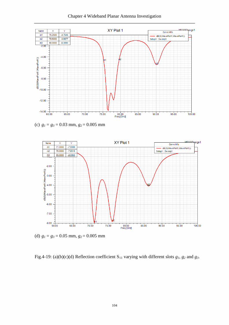
Chapter 4 Wideband Planar Antenna Investigation
104
(c) g1 = g3 = 0.03 mm, g2 = 0.005 mm
(d) g1 = g3 = 0.05 mm, g2 = 0.005 mm
Fig.4-19: (a)(b)(c)(d) Reflection coefficient S11 varying with different slots g1, g2 and g3.

Chapter 4 Wideband Planar Antenna Investigation
105
Fig.4-20: VSWR when g1 = g3 = 0.05 mm, g2 = 0.005 mm
In addition, the gap g2 could change the bandwidth as well, as shown in the VSWR
plot in Fig.4-21 where g2 = 0.001 mm, g2 = 0.01 mm and g2 = 0.02 mm, respectively.
It was observed that at high frequency around 90 GHz, the bandwidth achieved 6.6
GHz when g2 = 0.01 mm.
Fig.4-21: Red trace, g2 = 0.001 mm; Purple trace, g2 = 0.01 mm; Green trace, g2 = 0.05
mm

Chapter 4 Wideband Planar Antenna Investigation
106
4.2.9 Thickness of SiO2 Layer Effect
By increasing the thickness of SiO2 from 40 μm to 100 μm, the gain of the antenna
could have a better improvement. The gain at E and H plane is shown in Fig.4-22.
The highest gain marked as m1 achieved 5.15 dB while the highest directivity marked
as m2 reached 6.27 dB.
When the SiO2 layer thickness is 100 μm, less power was dissipated from the
substrate edge. Simultaneously, the signal returned back decreased to -20 dB and a
broadband was obtained as shown in Fig.4-23. More than 3 GHz frequency range
stayed below the standard, VSWR = 2, meaning that the antenna had a bandwidth of 3
GHz.
(a)

Chapter 4 Wideband Planar Antenna Investigation
107
(b)
Fig.4-22: (a) Radiation pattern of gain when H = 100 μm
(b) Radiation pattern of directivity when H = 100 μm
Fig.4-23: VSWR of U-shaped slot antenna when H = 100 μm

Chapter 4 Wideband Planar Antenna Investigation
108
4.2.10 Final U-shaped Slot Design Structure
The final design came out when the above parameters were considered into the
performance of the antenna. The parameters chosen in the final design are outlined in
Table 4-3
Table 4-3: Final parameter values chosen with a SiO2 substrate height of 40 μm
Parameters Value (mm)
Ground planar gw 0.25
gl 0.5
Feed a 10×fw
fx -0.25
“U” shape L1 0.14
L2 0.9
w1 0.4
w2 0.3
w3 0.4
Gaps g1 0.005
g2 0.001
g3 0.03
Fig.4-25 and Fig.4-25 show the maximum directivity and the gain of the antenna at
6.25 dB and 2.44 dB in both E and H plane, respectively. The antenna efficiency was
not high enough to radiate all the power out. The gain of this antenna was less than
half to that of the directivity. This was mainly caused by the narrow space, 40 μm
between the U-shaped slot patched antenna and the ground plane.
Chapter 4 Wideband Planar Antenna Investigation
109
Fig.4-24: Radiation pattern of antenna power gain in E, H plane with a 40 μm substrate.
Fig.4-25: Radiation pattern of antenna directivity in E, H plane with a 40 μm substrate.

Chapter 4 Wideband Planar Antenna Investigation
110
Fig.4-26 shows the reflection coefficient and bandwidth of the U-shaped slot antenna.
It was observed that the antenna had dual resonant frequencies very close to each
other.
Fig.4-26: Reflection coefficient and VSWR of the final structure U-shaped slot antenna
The simulation results shown in Fig.4-26 suggested that the U-shaped slot antenna
could operate at two resonant frequencies, 73.5 GHz and 76.5 GHz. However, the
bandwidths of these two frequencies were 1 GHz, which could not meet the
requirement of 3 Gbps HD data transmission. The main reason of narrow bandwidth
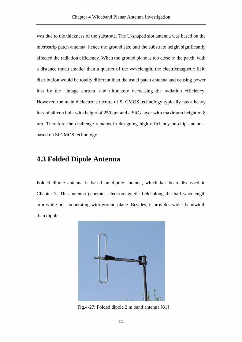
Chapter 4 Wideband Planar Antenna Investigation
111
was due to the thickness of the substrate. The U-shaped slot antenna was based on the
microstrip patch antenna; hence the ground size and the substrate height significantly
affected the radiation efficiency. When the ground plane is too close to the patch, with
a distance much smaller than a quarter of the wavelength, the electricmagnetic field
distribution would be totally different than the usual patch antenna and causing power
loss by the image current, and ultimately decreasing the radiation efficiency.
However, the main dielectric structure of Si CMOS technology typically has a heavy
loss of silicon bulk with height of 250 μm and a SiO2 layer with maximum height of 8
μm. Therefore the challenge remains in designing high efficiency on-chip antennas
based on Si CMOS technology.
4.3 Folded Dipole Antenna
Folded dipole antenna is based on dipole antenna, which has been discussed in
Chapter 3. This antenna generates electromagnetic field along the half-wavelength
arm while not cooperating with ground plane. Besides, it provides wider bandwidth
than dipole.
Fig.4-27: Folded dipole 2 m band antenna [81]

Chapter 4 Wideband Planar Antenna Investigation
112
Folded dipole antenna is based on dipole while both sides of the arm are ended with
elements, as shown in Fig.4-27. It has been reported that folded antennas can provide
a bandwidth enhancement of more than 50% [82, 83]. The basic structure of the
folded dipole antenna could be proposed on chip is shown in Fig.4-28. Some
investigation results proved that this antenna structure has the same wide bandwidth
as its two ends folded as a loop antenna [84].
The difference between d1 and d2 affects the input dipole impedance. Once the ratio d1
/ d2 = 1 / 3, a 100 Ω input impedance is obtained [84]. In order to match the
impedance at the feeding point, the feeder is chosen as a 100 Ω coplanar strip line
(CSP).
Fig.4-28: Parameters of a folded dipole antenna
To work at 60 GHz, the length of folded arm is required to be half wavelength, which
is 1.25 mm according to the SiO2 substrate. Strip width of the folded arm has a value
of d1 = 0.02 mm, d2 = 0.06 mm, respectively.

Chapter 4 Wideband Planar Antenna Investigation
113
4.3.1 Simple Folded Dipole Antenna Simulation
In the beginning, a simple folded dipole antenna based on the SiO2 substrate with a
relatively dielectric constant of 11.9, was simulated in Ansoft HFSS Ver.12.
Dielectric material SiO2 has a non-crystalline structure. It has electrical properties
such as low dielectric constant and low dielectric loss [85]. Thus, the loss tangent at
60 GHz can be ignored. In order to meet the needs of commercial use, centre
frequency of the antenna was designed to be 60 GHz. HFSS gave an analysis of 20
passes with the numerical delta of 0.02. The numerical delta in HFSS means the final
numerical error tolerance, which can be set by the user. The smaller the numerical
delta, the accurate the results will be. However, smaller numerical delta could
significantly prolong the computation time. Numerical delta of 0.02 was suggested by
the user manual. Antenna model simulated in HFSS Ver.12 was shown in Fig.4-29. It
was fed by a 100 Ω CPS with a space between the strips of 0.03 mm and a substrate
thickness of 40 μm. However the wave port needs to be designed with suitable size,
which will be discussed in Section 4.2.2. In this folded dipole antenna, it has a width
that is 2.5069 times of the feeder width.
Fig.4-29: HFSS simulation layout of a simple folded dipole antenna
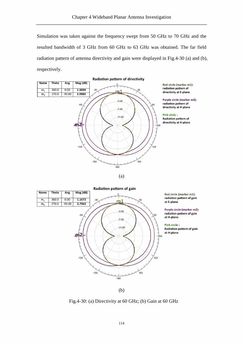
Chapter 4 Wideband Planar Antenna Investigation
114
Simulation was taken against the frequency swept from 50 GHz to 70 GHz and the
resulted bandwidth of 3 GHz from 60 GHz to 63 GHz was obtained. The far field
radiation pattern of antenna directivity and gain were displayed in Fig.4-30 (a) and (b),
respectively.
(a)
(b)
Fig.4-30: (a) Directivity at 60 GHz; (b) Gain at 60 GHz

Chapter 4 Wideband Planar Antenna Investigation
115
The radiation patterns showed a standard dipole pattern in E-field and a monopole
pattern in H-field because no ground plane was added on the bottom of the substrate.
In order to increase the antenna radiation gain and bandwidth, a cavity can be added
at the back of antenna, which will be discussed in Chapter 5.
4.4 Conclusion
In this chapter, a U-shaped slot antenna with 1 GHz bandwidth was investigated and
designed. Effects of U-shaped slot antenna dimension variables have been analysed
and discussed. According to the simulation results, the length of U-shaped slot patch,
L1 determined the radiation gain, the gap size, and the distance between two gaps
affect the bandwidth of antenna. By generating multiple resonant frequencies nearby,
the antenna bandwidth can be enhanced. However, distance between operating U-
shaped slot patch antenna and ground plane, i.e., the substrate height, also has effects
on the antenna bandwidth performance. Given that most Si CMOS technologies have
only a few micrometers thick SiO2 layer, this U-shaped slot antenna may have limited
applications for on-chip antenna realisation.
Folded dipole antenna was presented in the end of this chapter and proves to be able
to provide wider bandwidth. Further design of this folded dipole antenna with
metamaterials will be purposed in Chapter 5.

Chapter 5 AMCs for Millimetre-wave Antenna Application
116
Chapter 5
AMCs for Millimetre-wave Antenna
Application
5.1 Introduction
In Chapter 2, it has been indicated that recent millimetre-wave antenna design focuses
on the property of low cost and high performance. Si CMOS is the technology that is
used for mass production due to its low cost and high compatibility properties. It is
the foundation for a modern, digital world. Computer memory, CPUs, digital signal
processors and many other functional chips are made on Si CMOS. We wouldn‟t be
where we are now if there was no Si CMOS technology. Recently Si CMOS
technology has advanced from low frequency to microwave/millimetre-wave
applications. Si CMOS technology builds multiple metal layers on silicon bulk
substrate. Each metal layer is separated by a SiO2 layer. The multilayered structure of
this technology can be utilised to make a very compact circuit layout with the
integration of planar antennas, making it a very attractive alternative to conventional
GaAs MMIC technology for microwave/millimetre-wave applications. Si CMOS on-
chip antennas for millimetre-wave wireless communications, especially for 60 GHz

Chapter 5 AMCs for Millimetre-wave Antenna Application
117
home entertainment networks are highly desirable as they can significantly reduce the
cost. However, Si CMOS on-chip antennas suffer from high substrate loss, resulting
in low efficiency. Innovative design approaches will be key to successfully utilising
the Si CMOS technology for on-chip antenna applications.
As we discussed in Chapter 4, the primary limitation of on-chip antennas is the
bandwidth, which depends on the thickness of the structure with respect to the centre
wavelength. A U-shaped slot antenna may not be suitable for on-chip antenna
applications due to its restricted ground distance requirement. To reduce the influence
from the ground plane, two approaches can be taken: to have an antenna which is not
influenced by ground or to replace the ground metal plane with another reflective
material. The folded dipole antenna, however, generates electric current without the
help of a ground plane. We will study this antenna in details here.
In this chapter, we also introduce the AMC structure to the millimetre-wave antenna
design. AMC structure is a new type of metallic electromagnetic structure that has
been developed to have a HIS. This structure was first presented in 1999 [44]. It is
made of continuous metal but does not conduct AC current within a forbidden
frequency band. The difference between AMC and normal conductors is that this new
surface does not support propagating surface waves and also reflects electromagnetic
waves without phase change. All these properties make AMC suitable for replace the
normal conductive ground for reflecting electromagnetic waves without cancellation
caused by phase reversal. This chapter will discuss how AMC structure can be
applied to millimetre-wave antennas.

Chapter 5 AMCs for Millimetre-wave Antenna Application
118
In Sections 5.2 and 5.3, two cavities are added to the back of a half-wavelength folded
dipole antenna. They are a metal cavity that is made of a normal conductor and an
AMC cavity that consists of HIS structures. The theory as to how the AMC cavity
works and its applications will also be presented and discussed. Considering that an
antenna used at 60 GHz should have high efficiency, compatibility and low cost
properties, two novel antennas with newly reported AMC structures are also proposed,
designed and presented in Sections 5.4 and 5.5.
5.2 Antenna with Backed Metal Cavity
As discussed in Chapter 4, the U-shaped slot patch antenna results revealed that the
thickness of the dielectric substrate affects bandwidth performance. A better antenna
performance can be achieved by placing the antenna in a resonant cavity. In this
chapter, two types of cavities are designed to provide a resonant effect to a half-
wavelength folded dipole antenna that works at around 60 GHz. One of the reflector
cavities is formed by the AMC structure. The other is formed by a simple metal cavity.
AMC is built up with a well-arranged periodic metallic unit pattern and forms a pure
magnetic conducting plane with high surface impedance.
A resonant cavity is usually used as an electromagnetic resonator, in which the RF
signal propagating inside keeps vibrating. Since the cavity‟s surfaces are enclosed and
it only has one entrance, a specific cavity size causes a reflection to the wave at a
specific frequency. At that specific frequency, the RF signal incident is bounced
backwards and forwards within the cavity with low loss. Therefore resonant occurs.

Chapter 5 AMCs for Millimetre-wave Antenna Application
119
The standing wave intensity is increased during the resonant phenomenon, so that
more power will be radiated out and the antenna gain enhanced.
Bandwidth can be improved if the radiation device is suspended a distance H above
the ground plane [86]. Fig.5-1 gives the structure of the antenna backed by a metal
cavity. The folded dipole antenna is attached to the bottom of a 250 μm thickness
SiO2 substrate and placed in the centre of a 2.9 mm × 4 mm cavity.
Fig.5-1: Metal cavity structure in HFSS
Fig.5-2: Cross section of the metal cavity
Silicon Dioxide
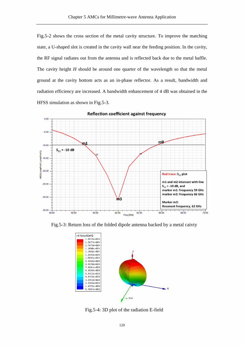
Chapter 5 AMCs for Millimetre-wave Antenna Application
120
Fig.5-2 shows the cross section of the metal cavity structure. To improve the matching
state, a U-shaped slot is created in the cavity wall near the feeding position. In the cavity,
the RF signal radiates out from the antenna and is reflected back due to the metal baffle.
The cavity height H should be around one quarter of the wavelength so that the metal
ground at the cavity bottom acts as an in-phase reflector. As a result, bandwidth and
radiation efficiency are increased. A bandwidth enhancement of 4 dB was obtained in the
HFSS simulation as shown in Fig.5-3.
Fig.5-3: Return loss of the folded dipole antenna backed by a metal caivty
Fig.5-4: 3D plot of the radiation E-field

Chapter 5 AMCs for Millimetre-wave Antenna Application
121
(a)
(b)
Fig.5-5: (a) Gain, 5.58 dB of the antenna with metal-cavity at resonate frequency
(b) Directivity, 5.77 dB of the antenna with metal-cavity at resonate frequency

Chapter 5 AMCs for Millimetre-wave Antenna Application
122
Fig.5-5 showed a radiation pattern of the antenna backed by a metal cavity at 62 GHz.
The simulated radiation efficiency at resonant frequency is 97.9%. Compared to the
gain obtained in Chapter 4, Gain increased from 2.44 dB to 5.58 dB.
The radiation pattern in Fig.5-5 indicates a better directivity compared to that without
the metal cavity, increasing to 5.77 dB. 3D plot of the E-field shows in Fig.5-6 was
generated by ten divisions of angle ϕ in azimuth plane of Fig.3-3 in order to speed up
the full wave simulation. Therefore it is not smooth and plump enough to present full
360 degree of angle ϕ. The cavity ground acts as a reflector and it reflects the
radiation power back to the feeder. As shown in Fig.5-6, the radiation pattern changed
its shape and gain is enhanced.
Fig.5-6: Radiation pattern with the effect of a reflector
5.3 Antenna in AMC Cavity
As discussed in Section 5.2, conductive surfaces such as the metal cavity can be used
as a reflector in antenna design [70].

Chapter 5 AMCs for Millimetre-wave Antenna Application
123
The reflector redirects nearly half the radiation wave in the opposite direction so that
the gain has a 3 dB (from 2.44 dB to 5.58 dB) improvement as Section 5.2 proved.
However, one must very careful when using a conductive surface to reflect the waves.
It reverses the phase of reflected waves by 1800 for a good conductor and forms a
zero electric field at the surface. Therefore when the electromagnetic wave travels
through the surface, the reflected wave changes its phase. This property results in the
image currents on the conductive sheet cancelling those currents in the antenna and
decreasing the radiation performance, if the distance between the antenna and the
reflector is very short. That said, the distance between the radiator (antenna) and the
reflector is restricted.
Fig.5-7: Antenna needs to be a quarter wavelength distance away from the conductive
reflector.
A method for solving the phase shift problem is to keep the antenna a quarter
wavelength from the reflector as indicated in Fig.5-7. A wave radiating out of the
antenna travels at a quarter wavelength and has a phase shift of π/2 when it reaches
the ground conductor. When the wave is reflected back by the ground, a 180 degree
phase shift is formed. By the time the wave travels back to the radiation element the
E-filed is superposed constructively, resulting in higher gain and efficiency.

Chapter 5 AMCs for Millimetre-wave Antenna Application
124
Another factor that affects the efficiency involved is the surface wave. Metal has a
property of supporting surface waves, which stays on the interface between the metal
and free space [87, 88]. For millimetre-wave communication those surface waves
equivalent to AC current exist along the metal surface plane. Once the surface is not
flat or smooth, the currents will radiate out and couple into the external plane wave. In
other words, if the conductive sheet is infinite, the current remains on the metal
surface. But in reality, the metal sheet has an edge and corner, so the current
propagating on it will be radiated out. As they are radiated to different directions than
the main lobe, in the far field radiation pattern, unwanted back lobes or other side
ripples are formed.
5.3.1 HIS Mechanism
In fact, the backed cavity cannot act as a reflector and improve the radiation if the
height is reduced significantly to less than a quarter of the wavelength. To reduce the
size of the antenna package, a new type of metallic electromagnetic structure was
developed early in 1999, which is called a high impedance electromagnetic structure
[44]. The structure is made of periodic metalised patterns. Unlike normal conductors,
it does not conduct ac current so it does not support surface wave propagation. The
cross section of a typical two-dimension HIS structure is shown in Fig.5-8. The
structure consists of a lattice of metal plates connecting with a metal sheet via a
vertical column conductor. Different from smooth conducting sheet that has low
impedance, this textured surface can have very high impedance.

Chapter 5 AMCs for Millimetre-wave Antenna Application
125
Fig.5-8: Cross section of a high impedance electromagnetic surface [44]
As some AMC structures have a property of HIS, the HIS structure is also called
AMC. HIS structure is formed with finite metal plates and has different geometrics
such as square, triangular, hexagonal, and circular etc. The top view of a typical
geometric hexagonal metal plate HIS structure is shown in Fig.5-9. The size of each
period is much smaller than the wavelength, as are the gaps between each of the
lattice elements.
Fig.5-9: Top view of a hexagonal HIS structure [44]
Since the hexagonal unit structure is much smaller compared to the wavelength, the
operational principle of the structure can be explained by using an equivalent lumped
LC circuit model. Fig.5-10 shows the side views of two adjacent units. As it can be
seen, the gap between the two hexagonal plates forms a gap capacitor and the other
connecting conductive elements act as inductors. That is, the gaps between
neighbouring metal patches produce capacitance and metal paths connections induce
inductance. The structure forms a parallel LC resonant tank, as shown in Fig.5-11. At
the resonant frequency, the LC resonant tank will resonate and result in very high

Chapter 5 AMCs for Millimetre-wave Antenna Application
126
surface impedance. In the other words, this surface is able to block the surface current
from flowing at the resonant frequency.
Fig.5-10: Single LC equivalent circuit
Fig.5-11: LC equivalent circuit for HIS structure
At around this resonant frequency, HIS can also act as a “magnetic conductor”. A
magnetic conductor is a virtual element. When the surface impedance is very high, the
tangential magnetic field is small whereas the electric field is large [89]. For example,
the Fig.5-12 shows the electric and tangential magnetic field plot on the magnetic
conductor surface. Over a specific frequency range, the magnetic conductor surface
has high impedance. Assuming an incident RF signal propagating on the surface with
E-field directing as Ei, the incident tangential magnetic field will be in Hi direction.
Due to the high impedance of the surface, the signal reflected back with the same
phase as Ei. Therefore the reflected E-field Er determined that the reflective tangential
magnetic field Hr is opposite to Hi. If perfect reflection occurs, Er = Ei, the electric
field is constructively added up whereas the magnetic field cancels each other out.

Chapter 5 AMCs for Millimetre-wave Antenna Application
127
Fig.5-12: E and H fields on magnetic conductor surface
The magnetic conductor has properties of high impedance and low loss, which can be
used as a new type of ground plane for low profile antennas. The new structure can
reflect waves. However, different from a flat conducting metal plane, the image
current produced on the plane and the wave in free space are in phase. Therefore the
requirement of distance between the antenna and the reflector can be greatly relaxed.
Theoretically, the antenna can be placed adjacent to HIS without causing any
destructive influence to the radiation pattern as shown in Fig.5-13.
Fig.5-13: An antenna placed closely to a HIS sheet

Chapter 5 AMCs for Millimetre-wave Antenna Application
128
In addition, the periodic texture structure supports are tightly bound, which leads the
Transverse Magnetic mode (TM mode) frequency to propagate much more slowly
along the surface. It also supports Transverse Electric mode (TE mode) that is bound
to the surface at some special frequency and radiates at some other frequency. Fig.5-
14 indicates the electric and magnetic field arrangement in TE mode propagation [90].
It can be seen from Fig.5-14, the magnetic field is extended out on the surface in
loops. The electric field is divided tangentially to both the radiation direction and the
surface. This kind of electromagnetic field arrangement does not support propagating
surface waves in a certain forbidden frequency band.
Fig.5-14: TE mode surface wave propagating on a HIS [44]
Thus the surface can be designed to have a special forbidden frequency band that
stops the surface wave generating on the high impedance conducting sheet. Without
the supporting of the surface wave in a forbidden bandwidth, a smooth radiation
pattern can be obtained and is independent to the effects of multipath interference
along the ground plane.
5.3.2 HIS design
According to different frequency and bandwidth requirements, HIS can be built to
meet the needs by properly designing the periodic structures. HIS structures work for
a large frequency range from several megahertz to tens of gigahertz. Referring to the

Chapter 5 AMCs for Millimetre-wave Antenna Application
129
prototype of HIS in Fig.5-8, one can find that there are several parameters that affect
the surface performance. The most primary is the thickness of the HIS structure
because it plays an important role in affecting the bandwidth performance. Take the
hexagonal shape that shows in Fig.5-14 as an example, the high impedance
electromagnetic structure consists of lattice of element. Each element has the shape of
a hexagonal metal plate and is connected together to the bottom solid metal sheet via
a conducting metal column.
Fig.5-15: Cross section and top view of a hexagonal HIS structure [91]
As discussed in Section 5.3.1, the period of these metal plate elements and the height
should be much less than the wavelength so that an efficient equivalent LC resonant
circuit can be obtained. The period of the structure that shows in Fig.5-15 is marked
as D, the hexagonal metal pattern has a scale of D. The gap, g, is formed between
nearby metal plates. The whole surface has a height, h, away from the bottom sheet.
Thus high surface impedance Zs is formed. On the top view, the hexagonal side has a
length of x, which has a relationship with pattern width, w.
According to the trigonometric function,
. (21)
xxw 32
32

Chapter 5 AMCs for Millimetre-wave Antenna Application
130
In the two layers structure, HIS can be described completely in terms of sheet
capacitance and sheet inductance because it was stated before that the HIS has an
equivalent circuit of parallel capacitors. In this section, the method of obtaining the
values of these parameters to make the most constructive improvement will be
discussed. Resonate frequency and radiation bandwidth can be expressed as follows:
Resonate frequency 𝜔0 =1
𝐿𝐶 (22)
The bandwidth equation relating to sheet capacitance and inductance was presented in
[92]. Radiation bandwidth for a narrow band antenna is percentage bandwidth and for
wide band antenna is called fractional bandwidth. The AMC structure has its own
resonant frequency as well and it can be considered a “natural frequency”, which is
𝜔0. Since in our design, 𝜔0= 60 GHz, radiation bandwidth of this structure can be
expressed as:
𝐵𝑎𝑛𝑑𝑤𝑖𝑑𝑡 =𝑓𝐻−𝑓𝐿
𝑓𝑐=
∆𝜔
𝜔0 (23)
In paper [92], it states that the electromagnetic radiation is due to the superposition of
antenna current and image current, while the radiated magnetic field is linked to the
electric field by the impedance of free space. Therefore the antenna current I can be
expressed as:
𝐼 = 𝐼𝑖𝑚𝑎𝑔𝑒 + 𝐻𝑟𝑎𝑑𝑖𝑎𝑡𝑖𝑜𝑛 =𝐸
𝑍𝑠+
𝐸
𝜂 (24)
where E is Electric field, 𝜂 is the resistance of free space, 𝑍𝑠 is the sheet impedance of
HIS and 𝑍𝑠 = 𝐿 𝐶

Chapter 5 AMCs for Millimetre-wave Antenna Application
131
From equation 24, we can see when the sheet impedance 𝑍𝑠 = 𝜂, the radiation drops in
half. The difference of these frequencies is ∆𝜔 and it can be estimated by substituting
𝜔0 = 1 𝐿𝐶 and 𝑍0 = 𝐿 𝐶 .
Finally, radiation bandwidth can be obtained from the characteristic impedance of the
surface divided by the impedance of free space, which is shown as:
𝐵𝑎𝑛𝑑𝑤𝑖𝑑𝑡 =𝑍0
𝜂=
𝐿
𝐶
𝜇 0𝜀0
= 𝜀0𝐿
𝜇0𝐶 (25)
where L and C are sheet inductance and sheet capacitance for the observation HIS
structure, respectively. , is the resonant frequency at which the reflection phase is
zero and the surface becomes a magnetic conductor. Adjusting the parameter values
to vary the value of L and C, any RF can be obtained. In reality the actual antenna
bandwidth may be smaller than the one calculated in equation 23. The bandwidth
obtained in the above equation can be seen as equivalent to the width of surface wave
band gap. However the enhancement function of a reflection wave depends on
different surface patch shapes and sizes as well.
To calculate the sheet capacitance and inductance C and L, a part of two nearby metal
patches are firstly taken into consideration.
Fig.5-16: A section of a hexagonal HIS structure design
0

Chapter 5 AMCs for Millimetre-wave Antenna Application
132
Fig.5-16 shows the surface sheet conductance geometry taking from HIS structure
prototype. In the structure, g is the gap width between two neighbouring hexagonal
plates and D is the distance between two centre units. Once the centre distance D >>
g, the electronic flux, , which generates around the gap can be obtained from
equation 30[44] as:
𝜍 = lim 2𝜀𝑉
𝜋cos−1
𝐷
𝑔 =
2𝜀𝑉
𝜋cosh−1
𝐷
𝑔
(26)
In this equation, is the permittivity on surface, V indicates potential voltage on
surface and electronic flux is a limitation value.
According to HIS structure shows in Fig.5-16, each hexagonal unit plate has a width
of w. Therefore, it assumes the surface has two values of different permittivity and the
individual capacitor width is w. Permittivity is in the radiation air space, while
another permittivity, , is produced by the HIS substrate. Since the sheet capacitance
has equal flux electrons on both sides, the equation of each conductor can be derived
from equation 26. Thus,
𝐶 =𝜍
𝑉=
𝑤 𝜀1+𝜀2
𝜋𝑐𝑜𝑠−1
𝐷
𝑔
)
(27)
The capacitance generated obeys the Guass‟ Law, which states that the amount of
charges on plates is proportional to the area of those plates. As the shape of each
patch is important in resonate frequency and bandwidth determination, a geometric
correction factor N is introduced to the individual capacitor calculation. The square
patch is taken as a reference, it has an area of , and , where
is the permittivity of the gap and g is the distance between two patches. According to
s
e
s
e1
e2
squareAg
AC
square
square
e

Chapter 5 AMCs for Millimetre-wave Antenna Application
133
the reference [44], each shape has its own patch surface area, , which can be
expressed as . The geometric correction factor N is the ratio of the
designed capacitor and the regular squared capacitor. Thus,
i.e.
(28)
Therefore the sheet capacitance can be obtained from equation 28. The factor N has
different values for different shapes as shown in Table 5-1.
Table 5-1: Sheet capacitance correction factor in various geometries
Different geometry Factor N
Square 1
Triangle
Round circle
Hexagonal
Sheet inductance relates to the thickness of the structure,
(29)
where, is the thickness of the HIS structure, is the permeability for free space
and is the relative permeability of the circuit board material. Derived from three
equations above, an equation of resonate frequency is obtained by substituting
sheet capacitance and inductance substituted into equation 22,
𝜔 =1
𝐿𝐶=
1
𝐿𝑠𝑒𝑒𝑡 ∙ 𝑁𝐶𝑠𝑞𝑢𝑎𝑟𝑒
=1
∙ 𝜇0𝜇𝑟 ∙ 𝑁 ∙𝑤 𝜀1+𝜀2
𝜋cosh−1
𝐷
𝑔
(30)
designedA
g
AC
designed
designed
squareddesigned CNC
square
designed
A
AN
3
4
3
1
sheetL
rsheet hL 0
h0
r
cf

Chapter 5 AMCs for Millimetre-wave Antenna Application
134
𝜔 is the centre frequency in radians, and 𝜔 = 2 ∙ 𝜋 ∙ 𝑓𝑐 ,
The centre frequency 𝑓𝑐 has an expression of
𝑓𝑐 =1
2𝜋 ∙ 𝐿𝑠𝑒𝑒𝑡 ∙ 𝑁𝐶𝑠𝑞𝑢𝑎𝑟𝑒
=1
2𝜋 ∙ ∙ 𝜇0𝜇𝑟 ∙ 𝑁 ∙𝑤(𝜀1+𝜀2)
𝜋cosh−1
𝐷
𝑔
(31)
Also the surface impedance can be calculated as:
𝑍𝑠 =𝑗𝜔𝐿
1 − 𝜔2 ∙ 𝐿 ∙ 𝑁𝐶𝑠𝑞𝑢𝑎𝑟𝑒 (32)
This is a new method of evaluating performance of HIS structure. It is based on
enhanced effective medium method, which was only used to evaluate the performance
of the square patch HIS structure [93]. According to the new method, other shapes of
patches can be designed more conveniently. Using this method some performance of
low profile antennas can be improved [94].
5.3.3 HIS Fabrication by PCB Technology
The basic AMC, a mushroom-shaped structure, forms high impedance on its surface
and can be fabricated by using PCB technology. The mushroom-shaped structure is a
two-dimensional structure. The two-layers HIS structure fabrication starts with
electrodepositing a copper layer on both sides of a plastic board to form a special
plastic board with metal layers on both sides. The process flow of making mushroom-
shaped structures on PCB technology can be summarized as shown in Fig.5-17. First,
a plastic board is covered with two copper layers and ready (Fig.5-17(a)). Holes are
then drilled vertically from the upper copper layer to the bottom copper layer, which

Chapter 5 AMCs for Millimetre-wave Antenna Application
135
are then prepared for building conducting vias. A thin plated metal is applied by using
the electroless process and forms a coating around the „via holes‟ and a photoresist
pattern is then used to etch the top metal layer (Fig.5-17 (b)). Finally the metal layer
is covered on the top layer (Fig.5-17 (c)).
Fig.5-17: Process flow of making mushroom-shaped structures on PCB technology
Most HIS structures need conducting vias to the ground to form the inductance.
Therefore, most of them have following common properties
a) A sheet of dielectric materials,
b) A series of parallel conductive strips on one side,
c) A conducting material layer on another side.

Chapter 5 AMCs for Millimetre-wave Antenna Application
136
Recently, HIS structures have been widely used to improve the performance of
antennas [95, 96]. For instance, HIS structure has been used on low observable
aircrafts because of its compact, relatively light and low cost properties.
HIS structures can be used as good electromagnetic isolators. In other words, HIS
structure can be applied to antenna arrays for anti-jamming applications. This is
because surface waves can be stopped by using HIS structures. Recently, multi-
layered HIS structures have been reported to achieve better performance, even with a
compact size [97, 98]. Each layer of patch units has its own sheet capacitance and
inductance. Certainly, a three-dimensional HIS structure requires a more complex
approach compared to a two-dimensional structure. In this work HIS structures were
designed and fabricated on Si CMOS technology.
5.3.4 Folded Dipole Antenna with HIS Cavity Backed
Simulation in HFSS
It has been discussed that theoretically the new metamaterial HIS structure has the
property of improving antenna performance without distance limitation. By applying
HIS structure as a reflecting ground in the cavity, a low profile antenna working at 60
GHz can have higher radiation gain. The antenna has the same structure as the one in
Section 5.2 while only the backed cavity has been changed. Fig.5-18 gives the
simulation structure in HFSS. Radiation antenna used is a 1.5 mm folded dipole
antenna fed by a 100 Ω CPS. The antenna is attached below a dielectric substrate with
a thickness of 250 μm. Antenna is suspending on the top centre of the cavity and a U-
shaped slot is built to have a better wave propagating from the feeder.

Chapter 5 AMCs for Millimetre-wave Antenna Application
137
Fig.5-18: Folded dipole antenna with a HIS cavity backed in HFSS structure
The cavity is enclosed with two kinds of HIS structures, hexagonal surfaces with
conducting via and corrugated metal slab. Hexagonal shaped HIS structure has
already been discussed in Section 5.3.2. The corrugated metal slab is another type of
structure that can provide high impedance at the top surface as well [99].
The details of this corrugated structure are shown in Fig.5-19. A series of slots are cut
vertically, and each slot is narrow and has a length of one quarter-wavelength deep.
When a wave propagates to the surface, it travels down to the bottom along the slab.
Equally, the structure can be regarded as a parallel plate transmission line, which is
shorted at one end and open at the other end. Thus impedance in the top is quite high.
In this project, corrugated metal slab is built around four vertical walls in the cavity.
This corrugated structure stopped surface wave propagation through improving the
radiation directivity.
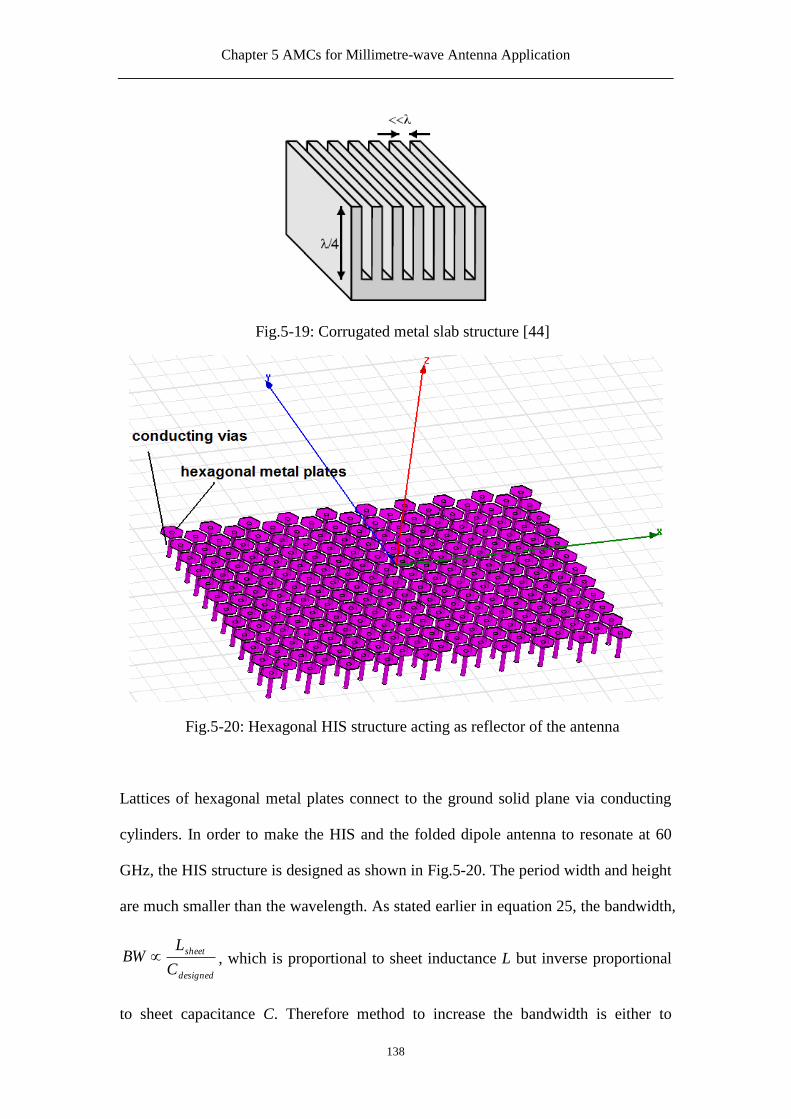
Chapter 5 AMCs for Millimetre-wave Antenna Application
138
Fig.5-19: Corrugated metal slab structure [44]
Fig.5-20: Hexagonal HIS structure acting as reflector of the antenna
Lattices of hexagonal metal plates connect to the ground solid plane via conducting
cylinders. In order to make the HIS and the folded dipole antenna to resonate at 60
GHz, the HIS structure is designed as shown in Fig.5-20. The period width and height
are much smaller than the wavelength. As stated earlier in equation 25, the bandwidth,
, which is proportional to sheet inductance L but inverse proportional
to sheet capacitance C. Therefore method to increase the bandwidth is either to
designed
sheet
C
LBW
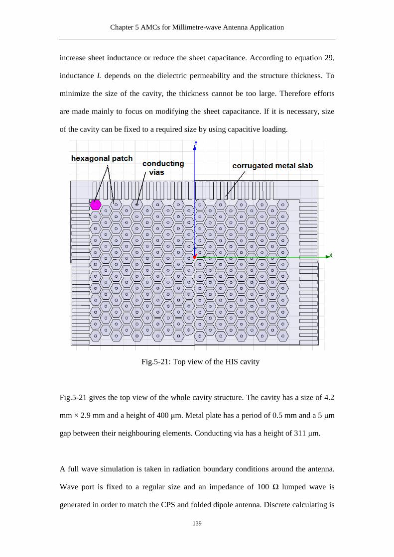
Chapter 5 AMCs for Millimetre-wave Antenna Application
139
increase sheet inductance or reduce the sheet capacitance. According to equation 29,
inductance L depends on the dielectric permeability and the structure thickness. To
minimize the size of the cavity, the thickness cannot be too large. Therefore efforts
are made mainly to focus on modifying the sheet capacitance. If it is necessary, size
of the cavity can be fixed to a required size by using capacitive loading.
Fig.5-21: Top view of the HIS cavity
Fig.5-21 gives the top view of the whole cavity structure. The cavity has a size of 4.2
mm × 2.9 mm and a height of 400 μm. Metal plate has a period of 0.5 mm and a 5 μm
gap between their neighbouring elements. Conducting via has a height of 311 μm.
A full wave simulation is taken in radiation boundary conditions around the antenna.
Wave port is fixed to a regular size and an impedance of 100 Ω lumped wave is
generated in order to match the CPS and folded dipole antenna. Discrete calculating is
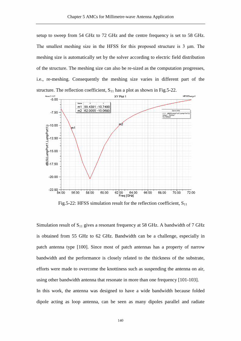
Chapter 5 AMCs for Millimetre-wave Antenna Application
140
setup to sweep from 54 GHz to 72 GHz and the centre frequency is set to 58 GHz.
The smallest meshing size in the HFSS for this proposed structure is 3 μm. The
meshing size is automatically set by the solver according to electric field distribution
of the structure. The meshing size can also be re-sized as the computation progresses,
i.e., re-meshing. Consequently the meshing size varies in different part of the
structure. The reflection coefficient, S11 has a plot as shown in Fig.5-22.
Fig.5-22: HFSS simulation result for the reflection coefficient, S11
Simulation result of S11 gives a resonant frequency at 58 GHz. A bandwidth of 7 GHz
is obtained from 55 GHz to 62 GHz. Bandwidth can be a challenge, especially in
patch antenna type [100]. Since most of patch antennas has a property of narrow
bandwidth and the performance is closely related to the thickness of the substrate,
efforts were made to overcome the knottiness such as suspending the antenna on air,
using other bandwidth antenna that resonate in more than one frequency [101-103].
In this work, the antenna was designed to have a wide bandwidth because folded
dipole acting as loop antenna, can be seen as many dipoles parallel and radiate
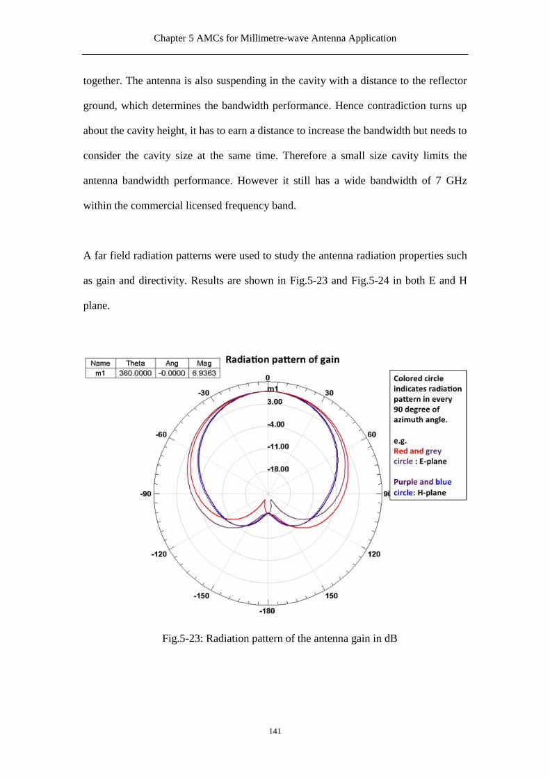
Chapter 5 AMCs for Millimetre-wave Antenna Application
141
together. The antenna is also suspending in the cavity with a distance to the reflector
ground, which determines the bandwidth performance. Hence contradiction turns up
about the cavity height, it has to earn a distance to increase the bandwidth but needs to
consider the cavity size at the same time. Therefore a small size cavity limits the
antenna bandwidth performance. However it still has a wide bandwidth of 7 GHz
within the commercial licensed frequency band.
A far field radiation patterns were used to study the antenna radiation properties such
as gain and directivity. Results are shown in Fig.5-23 and Fig.5-24 in both E and H
plane.
Fig.5-23: Radiation pattern of the antenna gain in dB

Chapter 5 AMCs for Millimetre-wave Antenna Application
142
Fig.5-24: Radiation pattern of the antenna directivity in dB
Radiation patterns in Fig.5-23 and Fig.5-24 show the gain and directivity at antenna
resonant frequency respectively. It can be seen that the gain at its maximum radiation
efficiency achieved 6.93 dB, which has a 1.5 dB enhancement compared to pure
metal cavity, comparing with diagram Fig.5-5(a). The same to the directivity, it has a
1.5 dB improvement than that with a simple metal cavity, shown in Fig.5-5(b).
Furthermore the radiation pattern becomes smoother and directional because it
drastically removed the back lobe. Fig.5-25 gives the 3D pattern plot of the gain,
which is more directivity than the one in Fig.5-4.

Chapter 5 AMCs for Millimetre-wave Antenna Application
143
Fig.5-25: Far field 3D plot of the antenna directivity
To sum up, the folded dipole antenna with high impedance electromagnetic surface
cavity backed obtains a smoother and more convergent far field radiation pattern. The
HIS cavity height is of 100 μm and a 7 GHz bandwidth is obtained. Comparison was
taken between two different cavities, structures in Fig.5-1 and Fig.5-18, respectively.
Simulation results showed that antenna operates in HIS cavity has a 1.5 dB gain
enhancement than the flat metal cavity. However, the height of conducting via (see
Fig.5-20), h = 311 μm, which makes the HIS cavity wall even thicker then the
resonant cavity height. Simulation results of this AMC cavity proved that HIS
structure can improve the antenna radiation gain with much decreased distance
between HIS reflector and antenna.
However, as discussed in section 5.3.2, height of conducting via, h determined the
sheet inductance, 𝐿𝑠𝑒𝑒𝑡 . To work at 60 GHz, 311 μm is the minimum height for h,
whereas the regular silicon bulk thickness in standard Si CMOS technology is 250 μm.

Chapter 5 AMCs for Millimetre-wave Antenna Application
144
That is to say, it will require extra efforts to build this structure on standard Si CMOS
technology. In Section 5.4 and 5.5, two other AMC structures with HIS property will
be proposed, they are planar and easy to fabricate.
5.4 Low Profile Patch Antenna with Micro-patterned
Artificial Lattice Plane
As discussed in Section 5.3, compares to the conventional metal cavity, folded dipole
antenna structure obtained a 1.5 dB gain enhancement from „hexagonal mushroom‟
and „conjugated slab‟ shaped HIS combining structure. Two on-chip antennas with
different AMC structures were designed, fabricated and characterised using two
different semiconductor foundries and they are presented the following two sections.
To have easier feeding structure and implementation by Si CMOS technology, the
patch antenna was used instead of the folded dipole
There normally are two methods to increase the bandwidth: apply an antenna on a low
dielectric constant material and increase the thickness of the dielectric layer. However,
neither of these two methods can be applied in Si CMOS technology, therefore,
additional elements which can improve antenna radiation performance must be
considered. When patch antenna operates at its resonant frequency, electric field
concentrates along the edge of patch. To enlarge the electric field at the edges, two
parallel strips are added to form a slot. This slot makes E-field coupled and boosted
up, in order to improve the bandwidth. The low-profile patch antenna designed with

Chapter 5 AMCs for Millimetre-wave Antenna Application
145
two adjusted strips is shown in Fig.5-26, for the two following AMC structure
application.
Fig.5-26: Improved patch antenna with two strips
5.4.1 Non-conducting Via AMC Structure Design
Our work used an AMC structure placing on the first metal layer of the wafer
fabrication process. As briefly introduced in Chapter 1, Si CMOS technology is a
frequently used to fabricate active and passive components. With this process, ICs
and devices are built upon oxidation material layer to avoid being affected by the
lossy silicon substrate. There are five main process steps applied in a standard Si
CMOS technology. They are oxidation (oxide grows on the silicon surface substrate
to form a layer of SiO2), diffusion (the impurity atoms on the surface moving into the
bulk material), ion implantation (ions are accelerated to a high velocity by the electric
field), deposition (mask is used to depose materials on silicon wafer) and etching
(remove exposed material and obtain one metal layer). Nevertheless, these five steps
are repeated on multi-layer Si CMOS technology.

Chapter 5 AMCs for Millimetre-wave Antenna Application
146
For example, the fabrication process we used was eight metal layers Si CMOS
technology from Chartered foundry. All these eight metal layers had been built by
sequence of five-steps on the silicon material substrate. As shown in Fig.5-27, metal
layers are labelled as M1 to M8 according to their layer positions, respectively.
Thickness of each dielectric layer, SiO2, is only 1 μm.
Fig.5-27: Eight metal layer Si CMOS process layout
Fig.5-28: Top view of square AMC unit structure
Fig.5-28 shows the unit metal plate which forms the periodic AMC structures. High
impedance could be generated on the surface within a frequency band. In the previous

Chapter 5 AMCs for Millimetre-wave Antenna Application
147
discussion of mushroom-shaped structure, a LC equivalent circuit was shown in
Fig.5-11, which derived impedance matches at LC resonant frequency. With a
conducting via connecting to the ground plane, plenty of works were successfully
done to improve the performance of passive components such as transmission lines,
antennas and filters [104-107].
Aimed to mass production and compatibility, Si CMOS process is the first choice as
the technology of component fabrication. However, structures with ground connecting
via cannot be implemented by Si CMOS technology according to the five-step
procedure. The AMC structure in this work only has one metal layer which consists of
periodic unit element showed in Fig.5-28. Capacitance and inductance of its
equivalent parallel LC circuit can be adjusted through parameters D, G. At 60 GHz,
the AMC metal period size, D, is smaller than the wavelength. The narrow gap
arranging at the edge of the square in the unit pattern requires G << D. As the antenna
designed in this work is a patch antenna that is fed by a 50 Ω microstrip line, eddy
current loss inside the shield becomes prominent at high frequency. Inserted between
the antenna plane and the silicon substrate, this structure of AMC plane blocks the
electric field from entering the substrate due to its high in-plane dielectric constant
[108]. The current density appears mainly around the edges of metal conductor,
cutting narrow slots close to the edges therefore to reduce the eddy current.
In Fig.5-29, a distinct microwave propagating path affected by the AMC structure is
shown. The AMC acting as a reflector reflected back the incident wave without phase
reversal. At the same time, the reflected wave takes part in the antenna radiation so as
the gain performance is enhanced.

Chapter 5 AMCs for Millimetre-wave Antenna Application
148
Fig.5-29: Distinct microwave propagating path
To observe the phase shift and reflection coefficient, AMC structure was simulated in
HFSS Ver.12. A master-slave boundary was used to simulate the infinite periodic
element plane. The incident wave starts from half-wavelength away off the AMC unit
surface.
A phase plot against frequency of reflecting wave S11 was made and shown in Fig.5-
30. It can be clearly seen that the phase equals to zero at 60 GHz frequency. Plot in
Fig.5-31 sketches the phase change in simulation model. According to Fig.5-31, we
assume the incident wave has a phase Phase1. After half wavelength propagating, the
phase of wave on AMC structure surface became Phase2, which is 180 degree shift
out of Phase1. As the phase of S11 that shows in Fig.5-30 equals zero, which means
the reflected wave Phase3 is in phase with incident. Propagating back half wavelength
to the AMC surface, Phase4 has a -180 degree phase shift out of Phase3. When taking
AMC surface as reference, the incident phase, Phase2, and the reflect phase, Phase4,
has null phase shift. Therefore, an artificial magnetic conducting plane was formed on
the surface.

Chapter 5 AMCs for Millimetre-wave Antenna Application
149
Fig.5-30: Simulated phase plot of S11
Fig.5-31: Simulated phase sketch of wave propagating
5.4.2 On-chip AMC Structure Antenna Design and Fabrication
Si CMOS substrate is lossy. To reduce the loss, AMC structure that shows in Fig.5-32
was investigated. The 1.212 mm × 1.111 mm sized AMC structure plane on the Si
substrate plays a role of a reflector. On the other hand, a patch antenna sized 0.4 mm

Chapter 5 AMCs for Millimetre-wave Antenna Application
150
× 0.4 mm with two additional parasitic elements was designed for broadening the
bandwidth of the antenna. As Fig.5-32(b) shows, the ground plane is locating at the
bottom of silicon bulk, which indicates the low resistivity silicon is used to be the
substrate of AMC.
(a)
(b)
Fig.5-32: (a) Simulate structure of patch antenna with AMC plane. (b) Side view of
structure layout

Chapter 5 AMCs for Millimetre-wave Antenna Application
151
Fig.5-32 shows the detail of the proposed antenna. It can be seen that the patch
antenna is located on the AMC plane. Two parallel strips adding on both sides can
wider the bandwidth. The G-S-G probe pads are added for measurement. The antenna
is fabricated through the 8 layers 0.13 μm Si CMOS process. As shown in Fig.5-27,
patch antenna is built on the top layer and the AMC structure stays on the first metal
layer. The thickness of 8 dielectric material layers is only 7 μm.
Results are shown in three parameters: the return loss S11, the operating frequency
gain and the directivity. Fig.5-33 shows simulated return loss of the patch antenna. It
can be noticed that the substrate loss is very high, especially at higher frequency. For
instance the loss above 80 GHz is more than 10 dB. For such high loss substrate, one
might not use VSWR < 2 to define the antenna bandwidth. The VSWR can be less
than -10 dB, but the RF power is dissipated by the substrate rather than radiate out to
the space. In Fig.5-33 the return loss from 72.5 GHz to 95 GHz clearly indicated that
the RF power has been radiated out to the space in addition to those dissipating to the
substrate. If we choose the bandwidth to be 10 dB lower than the power dissipated at
higher end of the frequency band, i.e., -20 dB in this study, the simulated bandwidth
shows in Fig.5-33 is approximately 5 GHz. Fig.5-34 and Fig.5-35 show the radiation
patterns of gain and directivity, respectively. In order to present the radiation patterns
in details, the patterns were cut along x-y plane, with angle ϕ in every 10 degrees. As
a result, plenty of traces are listing in the plot. Each colour shows one radiation
pattern at one cutting angle. For instance, the inner dark blue circle in Fig.5-34 shows
radiation pattern when ϕ = 90°, and while the outer red circle shows radiation pattern
when ϕ = 0°.
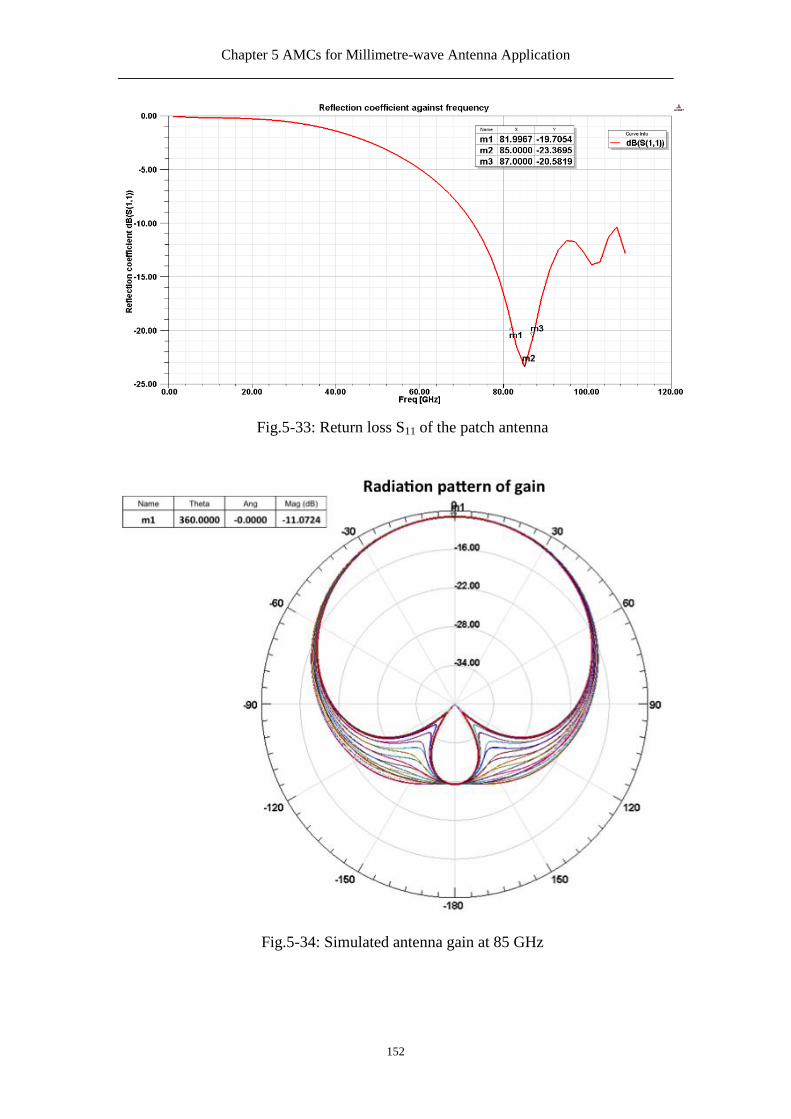
Chapter 5 AMCs for Millimetre-wave Antenna Application
152
Fig.5-33: Return loss S11 of the patch antenna
Fig.5-34: Simulated antenna gain at 85 GHz

Chapter 5 AMCs for Millimetre-wave Antenna Application
153
Fig.5-35: Simulated antenna directivity at 85 GHz
(a)

Chapter 5 AMCs for Millimetre-wave Antenna Application
154
(b)
Fig.5-36: (a) On-chip antenna measured by probe station system (b) Fabricated on-chip
antenna with AMC structure by 8 layer 0.13 μm Si CMOS process
The full structure of this AMC patch antenna was fabricated by 8 layers 0.13 μm Si
CMOS RF technology. On-chip antenna was fabricated by Chartered foundry. After
fabrication, antenna was measured by using GSG-100 probe station system shows in
Fig.5-36. Fig.5-36(a) shows the apparatus used to measure the on chip antenna.
Antenna was placed in the centre of metal chamber. A photo of on-chip AMC antenna
is shown in Fig.5-36(b) and the centre distance between two ground pads is 100 μm.
2-port network Cascade Microtech Model 11000 probe station provides GSG-100
probe to measure the antenna, HP 8510XF millimetre-wave controller and HP 8510c
network analyser were used to observe antenna reflection coefficient. As the foundry
requires that certain level of metal density for each metal must be satisfied, additional
strips were added around the sides of the antenna after design rule check (DRC). Due
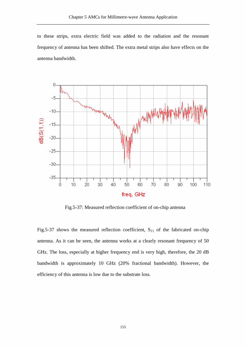
Chapter 5 AMCs for Millimetre-wave Antenna Application
155
to these strips, extra electric field was added to the radiation and the resonant
frequency of antenna has been shifted. The extra metal strips also have effects on the
antenna bandwidth.
Fig.5-37: Measured reflection coefficient of on-chip antenna
Fig.5-37 shows the measured reflection coefficient, S11 of the fabricated on-chip
antenna. As it can be seen, the antenna works at a clearly resonant frequency of 50
GHz. The loss, especially at higher frequency end is very high, therefore, the 20 dB
bandwidth is approximately 10 GHz (20% fractional bandwidth). However, the
efficiency of this antenna is low due to the substrate loss.
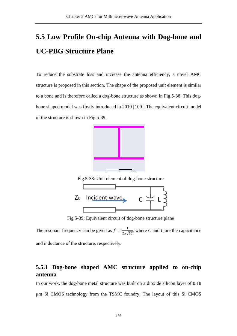
Chapter 5 AMCs for Millimetre-wave Antenna Application
156
5.5 Low Profile On-chip Antenna with Dog-bone and
UC-PBG Structure Plane
To reduce the substrate loss and increase the antenna efficiency, a novel AMC
structure is proposed in this section. The shape of the proposed unit element is similar
to a bone and is therefore called a dog-bone structure as shown in Fig.5-38. This dog-
bone shaped model was firstly introduced in 2010 [109]. The equivalent circuit model
of the structure is shown in Fig.5-39.
Fig.5-38: Unit element of dog-bone structure
Fig.5-39: Equivalent circuit of dog-bone structure plane
The resonant frequency can be given as 𝑓 =1
2𝜋 𝐿𝐶, where C and L are the capacitance
and inductance of the structure, respectively.
5.5.1 Dog-bone shaped AMC structure applied to on-chip
antenna
In our work, the dog-bone metal structure was built on a dioxide silicon layer of 0.18
μm Si CMOS technology from the TSMC foundry. The layout of this Si CMOS

Chapter 5 AMCs for Millimetre-wave Antenna Application
157
technology is shown in Fig.5-40. The first metal layer, M1, is etched on Interlayer
Dielectric (ILD) material, and two different dioxide silicon materials with different
dielectric constants are raised over M1. After the top metal layer, M6 finished etching,
conformal coating is covered for protection. Each group of dielectric material layers
has a thickness of 0.85 μm. Because atoms in dioxide silicon material can get excited
at high temperature, it may be unstable and even crack. Therefore the height of the
dioxide silicon material must be limited. The property of the Si CMOS process is
predestined to build any conducting vias with several hundred micrometers height. To
build in the Si CMOS process, only structures without vias meet the requirement.
Fig.5-40: 0.18 μm Si CMOS process from TSMC foundry model cross section [110]
Fig.5-41 shows the structure of this on-chip antenna. It can be seen that the ground
plane is located on M1, and the dog-bone structure lies on M2. Each of them has a
metal thickness of 0.53 μm and is separated by a 0.85 μm SiO2 layer. Upon the 4.99
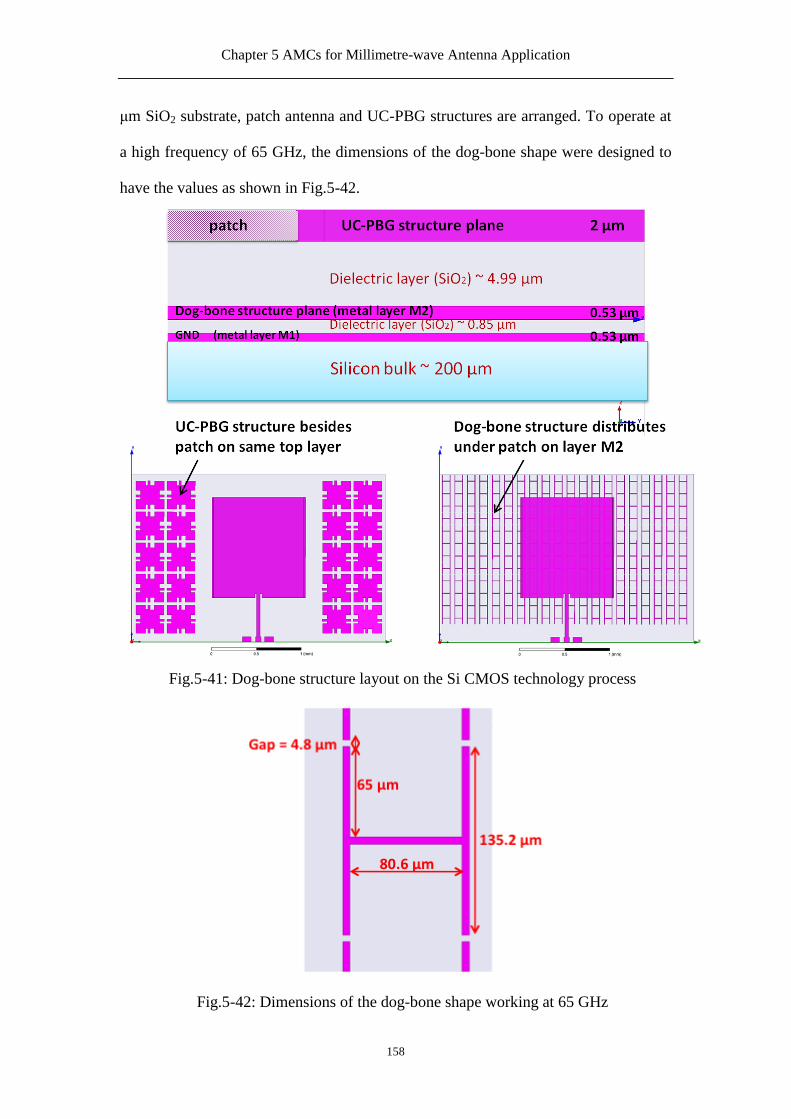
Chapter 5 AMCs for Millimetre-wave Antenna Application
158
μm SiO2 substrate, patch antenna and UC-PBG structures are arranged. To operate at
a high frequency of 65 GHz, the dimensions of the dog-bone shape were designed to
have the values as shown in Fig.5-42.
Fig.5-41: Dog-bone structure layout on the Si CMOS technology process
Fig.5-42: Dimensions of the dog-bone shape working at 65 GHz

Chapter 5 AMCs for Millimetre-wave Antenna Application
159
Fig.5-43: Simulated S11 phase plot of dog-bone unit using HFSS Ver.12
Full wave simulations of this dog-bone structure were carried out using HFSS Ver.12.
A master-slave boundary was used to simulate the infinite periodic element plane.
Distance from the wave input port to the surface of the unit plane was set to half-
wavelength. Therefore the incident wave would travel along a distance to make a
phase shift of 180 degree. The phase against frequency of reflecting RF signal S11 plot
is shown in Fig.5-43. It can be clearly seen that the phase shift is zero at 60 GHz.
5.5.2 UC-PBG Structure Applying to On-chip Antenna
To further increase the gain by suppressing the surface wave, a PBG structure is
incorporated with the proposed on-chip antenna. PBG structure was first proposed by
E.Yablonovitch in 1993 [37]. Recently it has been well developed in millimetre-wave
field. The first UC-PBG structure was proposed for microwave circuit application in

Chapter 5 AMCs for Millimetre-wave Antenna Application
160
1999 [111]. Also in that paper [111], a periodic grid consisting of PBG cells created a
forbidden frequency range so that the surface wave was stopped and reduced.
Fig.5-44: UC-PBG unit cell structure [112]
Fig.5-44 shows the unit cell of the UC-PBG structure. Each unit cell is patched above
ground with a dielectric material substrate on the secluded substrate. The structure
mainly contains a large square, and four narrow strips connect each unit together. The
connecting arm between two units acts as the inductor on the surface and the spaces
between units provides capacitance. As shown in Fig.5-44, the parameters of the UC-
PBG structure unit cell are marked with different variables. D is the period of the unit
cell, d is the distance between two squares, g is the gap between two neighbouring
units, m is the width of the small square in the corner, a is the width of the narrow
strip and t is the space between the small square and the narrow strip. To have the
UC-PBG structure working at the desired frequency, the parameters indicated in
Fig.5-44 are derived.
The relatively simple formulas used are based on the equations presented in [113,
114]. If the periodic grid consisting of a large number of UC-PBG cells can be
considered as a HIS with a grid impedance of equation 33 [114]
𝑍𝑔𝑟𝑖𝑑 =𝜌2
4
𝑗𝜔𝐶
1 − 𝜔2𝐿𝐶

Chapter 5 AMCs for Millimetre-wave Antenna Application
161
(33)
where ρ is the effective wave impedance of the substrate medium and ρ = ρ0 εe and
εe refers to the effective permittivity, which can be given as
εe = (εr + 1) 2 .
Where the relative constant is εr . If the unit period 𝐷 ≪ 𝑤𝑎𝑣𝑒𝑙𝑒𝑛𝑔𝑡 so that the
thickness of UC-PBG material is negligent, Grid capacitance, C, and inductance, L,
can be determined as [113, 114]:
C =2dεeε0
πln
2D
πa
L =μ0D
2πln
2D
πt
(34)
It can be seen from equation 33, if it is at resonant frequency 𝑓 =1
2𝜋 𝐿𝐶 , the factor
1 − 𝜔2𝐿𝐶 = 0, which means the grid impedance, 𝑍𝑔𝑟𝑖𝑑 equals to infinity. The surface
impedance of the UC-PBG structure can be calculated as a parallel connection of the
grid impedance and the wave impedance inside the dielectric substrate [115].
𝑍𝑠 =𝑍𝑔𝑟𝑖𝑑 𝑍𝑑
𝑍𝑔𝑟𝑖𝑑 +𝑍𝑑 ,
(35)
Where 𝑍𝑑 is the dielectric material impedance and 𝑍𝑑 = 𝜌0 𝜀𝑟 .
Therefore at resonant frequency, this periodic grid has the property of a HIS. Based
on the above equations, the UC-PBG unit cell structure was designed to have a = 24.7
μm, m = 108 μm , t = 37.5 μm , g = 35 μm , d = 250 μm and D = 315 μm in order to
operate at 65 GHz.

Chapter 5 AMCs for Millimetre-wave Antenna Application
162
5.5.3 AMC and UC-PBG On-chip Antenna Design and
Fabrication
In this work, the dog-bone shaped AMC structure plane and UC-PBG structures were
employed to combat the substrate loss and prevent surface wave propagation. The
employment of these two structures can improve antenna performance. The AMC
structure makes low profile antenna possible. Meanwhile, a UC-PBG structure was
built on the same layer surrounding the patch to stop the surface wave and further
increase the radiation gain at the operating frequency. The antenna is processed using
0.18 μm Si CMOS technology from the TSMC foundry. A wide bandwidth of 3.4
GHz from 64 to 67.8 GHz was obtained. The results showed a 1.6 dB gain
enhancement and an increase of more than 1 GHz bandwidth compared to the antenna
without AMC structures. The antenna radiation efficiency also exceeds 10%.
Fig.5-45: On-chip patch antenna with dog-bone AMC and UC-PBG model
The dog-bone structure and UC-PBG are printed on metal layers M2 and M6,
respectively, as shown in Fig.5-45. Each metal layer was separated by a 0.85 μm
dielectric layer. However, no metal is placed in layers M3 to M5 in this design, which
means the dielectric layer thickness in this work became 4 × 0.85 μm + 3 × 0.53 μm =
4.99 μm. Traditional patch antenna located a 4.99 μm distance above ground would

Chapter 5 AMCs for Millimetre-wave Antenna Application
163
have poor bandwidth and efficiency, due to the imaging current effect. With the help
of the AMC structure, performance is improved significantly. The structure was
firstly simulated in HFSS Ver.12. The main parameters, reflective coefficient,
directivity and gain, were observed.
The S11 simulation result is shown in Fig.5-46 and indicates the bandwidth of 3.2
GHz from 64.6 GHz to 67.8 GHz. The patch antenna designed in this work was fed
by a 50 Ω microstrip line with a patch size of 1.13 mm × 1.01 mm. Two strips are
placed 5 μm away from each sides. Fig.5-47 presents the E-field existing on patch
antenna and UC-PBG patterns. Most of the E-field is located at the edge of the patch
antenna instead of leaking to the side as a surface wave.
Fig.5-46: S11 simulated result

Chapter 5 AMCs for Millimetre-wave Antenna Application
164
Fig.5-47: E-field existing on patch antenna and UC-PBG patterns
Fig.5-48 plots the antenna gain as a radiation pattern including E-H plane. The
simulated gain is of -10.07 dB at an operating frequency of 65.5 GHz. However, the
pattern has clear directivity and small back lobe. This is due to the AMC plane
located under the patch antenna reflecting the signal to radiate without flowing
sideways. The simulation of a traditional patch antenna has been done for comparison
purposes. The gain of on-chip patch antenna at operating frequency is shown in Fig.5-
49. According to this result, the gain of the antenna with AMC and UC-PBG has
improved by 1.6 dB.

Chapter 5 AMCs for Millimetre-wave Antenna Application
165
Fig.5-48: Radiation pattern of on-chip AMC and UC-PBG antenna gain at 65.5 GHz
Fig.5-49: Radiation pattern of on-chip traditional patch antenna gain at 65.5 GHz

Chapter 5 AMCs for Millimetre-wave Antenna Application
166
Fig.5-50: Fabricated on-chip AMC and UC-PBG structured antenna layout
In addition to the simulation, this antenna was also fabricated by the TSMC foundry
using 0.18 μm Si CMOS technology. Fig.5-50 is a photo of the fabricated antenna. A
Cascade Microtech Model 11000 probe station, an HP 8510XF millimetre-wave
controller and an HP 8510c network analyser were used as the measurement
apparatus. Both measured and simulated S11 are shown in Fig.5-51. In this plot, the
purple dashed curve represents S11 of the traditional on-chip patch antenna. The red
and blue curves represent the simulated and measured S11 results of the AMC and
UC-PBG structured on-chip patch antennas, respectively. They clearly shows that the
bandwidth increased by more than 1 GHz.

Chapter 5 AMCs for Millimetre-wave Antenna Application
167
Fig.5-51: Reflection coefficient results
5.6 Conclusion
In this chapter, we focused on designing low profile on-chip antennas for millimetre-
wave application. As the silicon material in Si CMOS technology has low resistivity,
Si substrate is so lossy that antenna efficiency would be very low. To avoid the lossy
Si substrate, a dielectrical layer on standard Si CMOS technology is used instead.
However, the thin thickness of the SiO2 layer reduces the radiation efficiency. As has
been discussed in Chapter 4, on-chip antenna could be successfully designed if the
effect from the conductive ground plane could be eliminated. The AMC structure was
used to solve this issue.
In the beginning, two folded dipole antennas with different cavities were proposed,
simulated and discussed. Two cavities were made of different materials, one with
normal conductive metal and the other with the AMC structure. Full wave simulation
results in HFSS showed that the AMC structure provided an enhancement on a gain

Chapter 5 AMCs for Millimetre-wave Antenna Application
168
of 1.5 dB, compared to the radiation gain obtained from a normal metal cavity. The
AMC structure cavity consists of a mushroom structure and corrugated slabs. Both of
these structures are in three dimensions, which increase the total antenna size and
become hard to fabricate.
Two other AMC structures with HIS properties were designed, simulated and
fabricated from two Si CMOS foundries. Both antennas are based on low profile
patch antennas with two parasitic strips to increase their radiation bandwidth.
According to the Si CMOS technology, the on-chip antenna proposed in Section 5.4
was built with a micro-patterned artificial lattice plane and this AMC structure was
placed on the first metal layer of the process. After being fabricated by Si CMOS
process from the Chartered foundry, the proposed antenna was measured.
Measurement results showed the on-chip antenna resonant at 50 GHz with a 20 dB
bandwidth of 10 GHz. In reality, the antenna integrity has been changed by the
foundry during the fabrication to meet the metal density requirement. The Chartered
foundry requires that metal located on each layer must meet the standard density.
However the patch antenna on the top metal layer is too small to achieve the
requirement. Therefore, additional metal strips around the antenna and AMC
structures were added in order to pass the DRC required from the foundry. As a result,
the effective antenna size has been enlarged and the resonant frequency decreased.
The substrate loss due to the silicon material in this antenna is high, especially at
higher frequencies. For this high loss structure, we define the bandwidth as -10 dB
lower than the power dissipated at the higher end of the frequency band, which is –20
dB. That is to say, the bandwidth that shows in the measurement result is
approximately 10 GHz, which is 20% of the fractional bandwidth.

Chapter 5 AMCs for Millimetre-wave Antenna Application
169
Although the bandwidth of the antenna structure in Section 5.4 is large, the substrate
loss dissipated most of the RF wave power. In Section 5.5, the AMC structure and
metal layer arrangement was improved. A novel on-chip antenna with a dog-bone and
UC-PBG structure plane was designed, fabricated and proposed. A ground plane was
put on the first metal layer of the Si CMOS process to isolate the antenna from the
lossy silicon substrate. A regularly arranged dog-bone shaped AMC structure was
placed on the second metal layer (M2), which formed an RF wave reflection without
phase reversal. The patch antenna with parasitic strips was located in the centre of the
top metal layer and it was surrounded by a UC-PBG structure to prevent surface wave
loss. Fabrication was done by the TSMC foundry and the measurement results show
that this on-chip antenna operates at 65.5 GHz with a bandwidth of 3.2 GHz.
Compared to the simulation bandwidth of the patch antenna without an AMC
structure, the AMC and UG-PBG structured antenna has gained a bandwidth rise of
more than 1 GHz and 1.6 dB higher gain.
According to the specification, the on-chip antennas proposed resonate at millimetre-
wave frequency and have a bandwidth of 3.2 GHz, which is enough for the HD data
transfer requirement of 3 Gbps. However the gain of this proposed antenna is -10.07
dB, which is 1.6 dB higher than traditional on-chip patch antenna without AMC.

Chapter 6 On-chip Antenna Fabrication and Measurement
170
Chapter 6
On-chip Antenna Fabrication and Measurement
6.1 Measurement Setup
On chip antenna is an attractive but challenging topic. The most often concerned is
the silicon bulk loss. Low resistivity of silicon substrate kills energy heavily at high
frequency. As a one-port network, reflection coefficient is obtained to observe
antenna radiation. The main measurement apparatus used in our work are shown in
Fig.6-1.
Fig.6-1: Measurement apparatus of on-chip antenna

Chapter 6 On-chip Antenna Fabrication and Measurement
171
As on-chip antenna was designed to compact into millimetre-wave communication
devices, it needs to be stable performance even if surrounding temperature changes.
In this chapter, the relationship between these two proposed on-chip antennas and
temperature will be investigated and discussed. As the size of antenna is very small,
we use GSG-100 probe station to measure. However, it is not easy to put probe station
into a chamber room to measure the gain. Followed the temperature observation, we
chose another method to detect antenna gain. The method and results will be
presented.
6.2 Reflection Coefficient Changes with Temperature
Based on two structures presented in Section 5.4 and Section 5.5, relationship
between reflection coefficient and temperature was observed. Each antenna was
placed in the probe station, which is well located by a chamber. The temperature of
the chamber can be change within a various range from -75 Celsius to 200 Celsius by
temperature controller, as shown in Fig.6-2.
Fig.6-2: Temperature controller

Chapter 6 On-chip Antenna Fabrication and Measurement
172
Normal steady flow of air was infused into the probe station chamber from the gas
dryer is shown in Fig.6-1. Humidity needs to be decreased to a suitable standard.
Otherwise, the surface of measuring device will raise mist or even ice at low
temperature.
6.2.1 Temperature Measurement of One Layer AMC Structured
Antenna
Firstly the on-chip antenna with one layer AMC structure was measured at five
different temperatures. This antenna was fabricated by Chartered foundry. Fig.6-3
gave the testing antenna layout.
Fig.6-3: Single layer AMC structure antenna measuring in probe station
The Reflection coefficient plot against frequency is measured and shown from Fig.6-4
to Fig.6-8. Plot was taken at five different temperatures: -57 Celsius, 0 Celsius, 20
Celsius (room temperature), 75 Celsius and 145 Celsius. The bandwidth variations

Chapter 6 On-chip Antenna Fabrication and Measurement
173
with temperature were investigated. Due to the Si substrate loss, 20 dB (instead of 10
dB) bandwidth was examined.
Fig.6-4: Reflection coefficient at room temperature (20 Celsius)
Fig.6-5: Reflection coefficient at 0 Celsius

Chapter 6 On-chip Antenna Fabrication and Measurement
174
Fig.6-6: Reflection coefficient result at -57 Celsius
It can be seen from these three results in Fig.6-4, Fig.6-5 and Fig.6-6, bandwidth
keeps increasing along with temperature decreasing. However the average in-band
reflection coefficient decreased with temperature. Further two more measurements
were made to prove this trend as shown in Fig.6-7 and Fig.6-8.
Fig.6-7: Reflection coefficient result at 75 Celsius
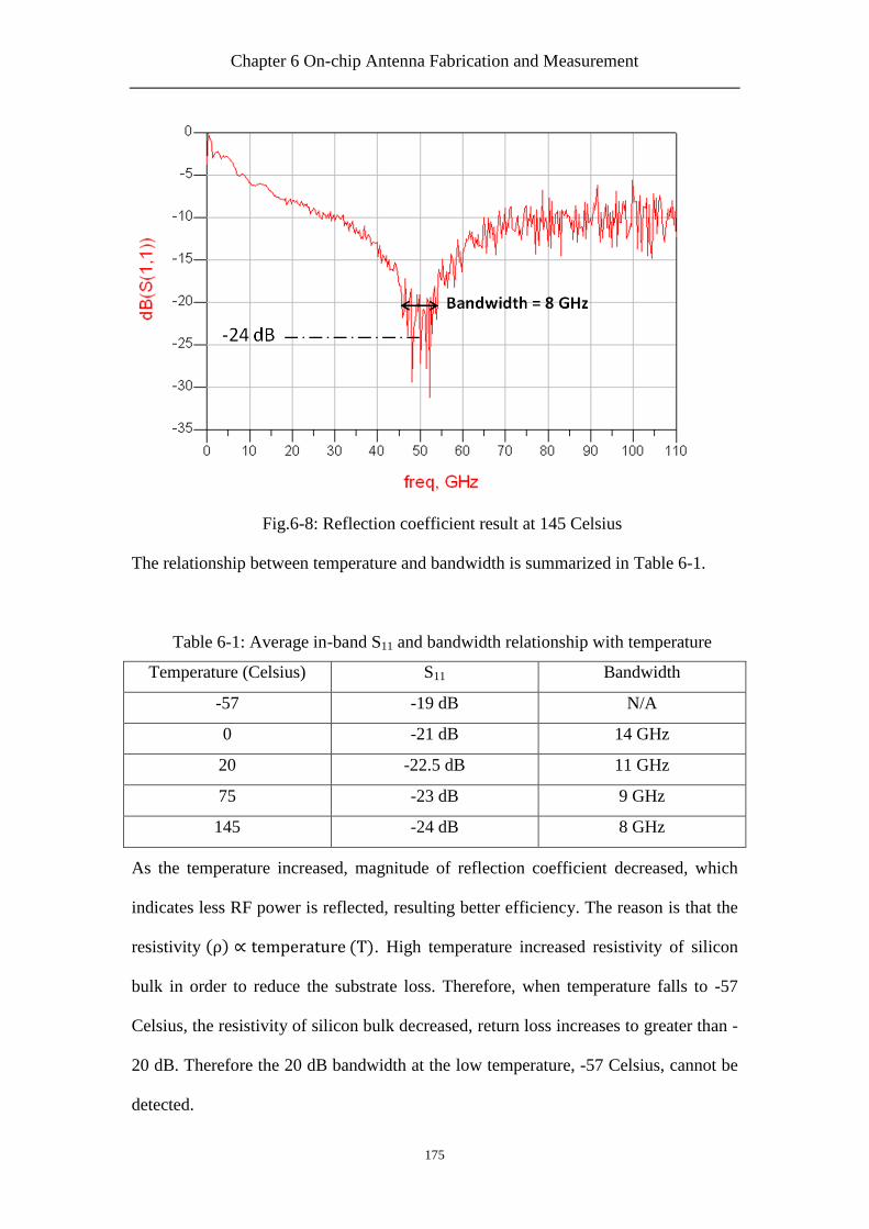
Chapter 6 On-chip Antenna Fabrication and Measurement
175
Fig.6-8: Reflection coefficient result at 145 Celsius
The relationship between temperature and bandwidth is summarized in Table 6-1.
Table 6-1: Average in-band S11 and bandwidth relationship with temperature
Temperature (Celsius) S11 Bandwidth
-57 -19 dB N/A
0 -21 dB 14 GHz
20 -22.5 dB 11 GHz
75 -23 dB 9 GHz
145 -24 dB 8 GHz
As the temperature increased, magnitude of reflection coefficient decreased, which
indicates less RF power is reflected, resulting better efficiency. The reason is that the
resistivity ρ ∝ temperature (T). High temperature increased resistivity of silicon
bulk in order to reduce the substrate loss. Therefore, when temperature falls to -57
Celsius, the resistivity of silicon bulk decreased, return loss increases to greater than -
20 dB. Therefore the 20 dB bandwidth at the low temperature, -57 Celsius, cannot be
detected.

Chapter 6 On-chip Antenna Fabrication and Measurement
176
6.2.2 Temperature Measurement of Dog-bone AMC and UC-
PBG Structured Antenna
This on-chip antenna, which shows in Fig.6-9 was measured by the same equipment
and procedure as Section 6.2.1. Fig.6-10 shows S11 plot at the temperature of 15
Celsius. Ten groups of data were collected at different temperatures. Reflection
coefficient values of antenna operating at those temperatures are measured and
recorded in Table 6-2.
Fig.6-9: Dog-bone AMC and UC-PBG antenna in temperature measurement
Fig.6-10: S11 plot at 15 Celsius temperature

Chapter 6 On-chip Antenna Fabrication and Measurement
177
Table 6-2: Average in-band reflection coefficient S11 changing with temperature
Temperature in Celsius S11
-25 -10.881 dB
-20 -10.992 dB
0 -11.438 dB
15 -12.340 dB
25 -12.470 dB
50 -12.993 dB
70 -13.513 dB
105 -13.721 dB
120 -15.133 dB
150 -16.099 dB
Fig.6-11: Reflection coefficient against temperature plot
Plot in Fig.6-11 further proved, as already seen in Section 6.2.2 that antenna
efficiency increased along with temperature. In a fact, increasing of the resistivity
brings higher efficiency of the antenna.

Chapter 6 On-chip Antenna Fabrication and Measurement
178
6.3 Gain Measurement of On-chip Antenna
On-chip antennas at millimetre-wave band are very small. The probe station setup
makes it very difficult to measure the antenna radiation patterns. This is because the
surroundings of the probe station and even the probe itself (which is hundreds time
bigger than the antenna itself), as it can be seen in Fig.6-12, severely disturb the
radiation path for any possible accurate measurement. Furthermore it is impossible to
make neither transmitter antenna nor receiver antenna to rotate, which is required for
radiation pattern measurement. To overcome these measurement shortages, only
antenna gains were measured.
Fig.6-12: On-chip antenna and probe station

Chapter 6 On-chip Antenna Fabrication and Measurement
179
Two same on-chip antennas were used to measure the antenna radiation transmission
performance. Two on-chip antennas were placed apart and acting as transmitter and
receiver. A 2-port network is formed with these two antennas. Measurements were
taken from S-parameter values of this 2-port network by VNA. In order to have more
accurate measurement results, plenty of positions were chosen. They were indicated
from P1 to PN according to their position to the antenna from transmitter. Due to the
limitation of the probe station, the furthest measuring distance is 8 mm, any points
that is more than 8 mm away from no signal can be detected by the VNA.
Twenty positions in far-field range were measured. According to Far-Filed range
definition, area out of sphere with radius R =2L2
λ is called far-field range. As Fig.6-13
shows, two antennas operating at 65.5 GHz should be placed at least 1.11 mm apart to
measure the far-field radiation gain.
Fig.6-13: Far field determination

Chapter 6 On-chip Antenna Fabrication and Measurement
180
Fig.6-14: Antenna measurement position plot
Fig.6-14 plots out each measurement position, where the transmitter antenna is fixed
at the centre and the receiver antenna changes its positions to measure the
transmission performance. The rectangular in the centre represents the on-chip
antenna acting as transmitter and P1, P2 …PN representing the positions of receiver
antenna. For instance, the purple rectangular represents transmit antenna and at
position P20, the pink rectangular indicates receive antenna facing to the transmit one.
The arrow shows the direction of measurement probe and dash circle indicates the far-
field range of the transmitter antenna. Totally twenty groups of 2-port S-parameters
data are recorded and displayed in Table 6-3.

Chapter 6 On-chip Antenna Fabrication and Measurement
181
Table 6-3: Data collection from twenty different positions
Position Distance S11 (dB) S22 (dB) S12 (dB) S21 (dB)
P1 2 mm -14.11 -13.06 -44.25 -44.64
P2 2 mm -13.21 -12.37 -56.27 -54.68
P3 2 mm -12.44 -12.52 -53.52 -53.50
P4 2.83 mm -12.90 -13.13 -56.63 -56.23
P5 2.83 mm -18.74 -25.37 -44.31 -44.38
P6 2.83 mm -13.91 -12.37 -56.36 -55.47
P7 2.83 mm -15.80 -12.96 -54.30 -54.99
P8 4 mm -12.72 -12.24 -46.13 -45.48
P9 4 mm -12.80 -13.08 -58.05 -58.50
P10 4 mm -14.11 -13.05 -53.25 -53.14
P11 5.66 mm -11.90 -11.80 -58.86 -57.82
P12 5.66 mm -12.70 -12.90 -57.90 -55.00
P13 5.66 mm -13.09 -12.45 -58.64 -56.24
P14 5.66 mm -12.30 -12.04 -57.82 -55.61
P15 6 mm -19.48 -14.37 -52.06 -50.08
P16 6 mm -11.76 -12.61 -63.11 -63.05
P17 6 mm -15.96 -13.37 -53.51 -52.01
P18 8.49 mm -11.40 -14.53 -57.74 -57.08
P19 8.49 mm -11.90 -14.53 -57.23 -55.80
P20 8 mm -13.06 -12.86 -54.84 -55.23

Chapter 6 On-chip Antenna Fabrication and Measurement
182
Fig.6-15: S21 measurement result at different position
Fig.6-16: S11 measurement result at different position
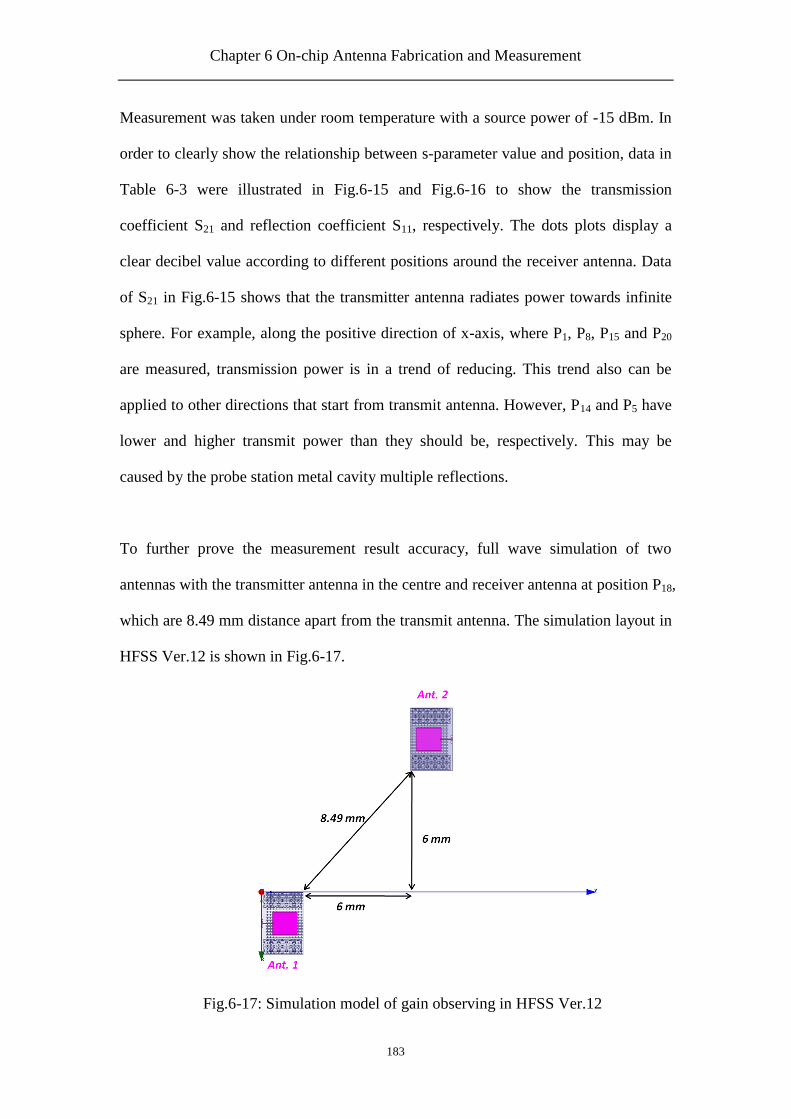
Chapter 6 On-chip Antenna Fabrication and Measurement
183
Measurement was taken under room temperature with a source power of -15 dBm. In
order to clearly show the relationship between s-parameter value and position, data in
Table 6-3 were illustrated in Fig.6-15 and Fig.6-16 to show the transmission
coefficient S21 and reflection coefficient S11, respectively. The dots plots display a
clear decibel value according to different positions around the receiver antenna. Data
of S21 in Fig.6-15 shows that the transmitter antenna radiates power towards infinite
sphere. For example, along the positive direction of x-axis, where P1, P8, P15 and P20
are measured, transmission power is in a trend of reducing. This trend also can be
applied to other directions that start from transmit antenna. However, P14 and P5 have
lower and higher transmit power than they should be, respectively. This may be
caused by the probe station metal cavity multiple reflections.
To further prove the measurement result accuracy, full wave simulation of two
antennas with the transmitter antenna in the centre and receiver antenna at position P18,
which are 8.49 mm distance apart from the transmit antenna. The simulation layout in
HFSS Ver.12 is shown in Fig.6-17.
Fig.6-17: Simulation model of gain observing in HFSS Ver.12

Chapter 6 On-chip Antenna Fabrication and Measurement
184
The receiver antenna, Ant.2 has a distance 8.49 mm apart from the transmitter and its
distance to x and y axis is 6 mm. Fig.6-18 is the plot of two S-parameters, S11 and S21.
M1 is a marker of S11 and M2 is the marker of S21. Simulation result shows two
antennas resonant at 65 GHz and the value of S21 is -57.35 dB.
Fig.6-18: S11 and S21 plot in simulation
Fig.6-19: Simulated radiation pattern at the plane with P18 of Ant 2 at 65 GHz

Chapter 6 On-chip Antenna Fabrication and Measurement
185
As it is impossible, to turn the GSG probe station in an angle to measure the radiation
pattern, two antennas were placed on the same plane for the transmission coefficient
measurement, which is shown in Fig.6-12. Therefore at position P18, power
transmitted into Ant 2 is not all power that radiates out. In Fig.6-19, radiation pattern
of gain was plot when ϕ = 135°, where P18 locates. Marker M1 indicates the exactly
gain obtained at P18. The gain at P18 equals to -15.92 dB. It should be pointed out that
this is not the maximum gain. It is the gain at ϕ = 135°. The maximum radiation
power gain is where marker M2 indicates, -9.12 dB. Simulation result in Fig.6-19
shows that the transmitter antenna has a maximum gain of -9.12 dB, as marker M2
shows. Compared to the radiation gain that shows in Fig.5-48, radiation gain of
antenna increased from -10.07 dB to -9.12 dB. The 0.9 dB gain enhancement is due to
the effect of receiver antenna.
As the antenna received power, 𝑃𝑟 , can be expressed as [116]:
𝑃𝑟 = 𝑃𝑡
𝐺𝑡𝐺𝑟 ∙ 𝜆2
(4𝜋𝑅)2
(36)
where 𝑃𝑡 is the transmit power from Ant 1, 𝐺𝑡 and 𝐺𝑟 are gain of transmit and receive
antennas, in this case, 𝐺𝑟 and 𝐺𝑡 are the same and equals to the antenna received gain.
𝜆 is the wavelength in free space and 𝑅 is the distance of two antennas. Also the
transmit coefficient S21 is the ratio of power received to power transmitted,
𝑆21 = 10log(𝑃𝑟
𝑃𝑡)
(37)
Substituted equation 37 into equation 36, the received antenna gain can be estimated.
In Table 6-3, measured S21 at P18 is -57.08 dB and the received gain can be calculated
to be -14.89 dB. Comparing to the simulation result that is shown in Fig.6-19, the

Chapter 6 On-chip Antenna Fabrication and Measurement
186
measured gain (calculated based on measured S21) is approximately 1 dB lower than
that simulated, which is quite acceptable given that the simulation setup is not quite
the same as the measurement one. For instance, there is no probes in the simulation
and the boundary in the simulation hardly mimics the probe station cavity and its
surroundings.
6.4 Conclusion
In this chapter, two low profile AMC Si CMOS on-chip antennas proposed in Section
5.4 and Section 5.5 were fabricated and characterised. Effects of temperature
variation on the AMC antennas were also examined experimentally.
Since the AMC on-chip antenna needs to be measured using probe station used in our
work is hundreds times larger than the antenna, it is impossible to move the probe
station into an anechoic chamber. It is also impossible to rotate the probe to measure
the radiation pattern using our existing facility. An alternative way was adopted to
measure the gain performance of the on-chip antennas by measuring transmission
coefficient, S21, between two exactly the same antennas, one as transmitter and the
other as receiver in different positions around the transmit antenna. The measurement
results seem agreeing with simulated ones reasonably well.
Chapter 7 Conclusion and Future work
187
Chapter 7
Conclusion and Future Work
7.1 Summary of the Work
Since unlicensed band around 60 GHz was announced, millimetre-wave technology
had rapidly and substantially developed. In the beginning of this thesis, considerations
of millimetre-wave devices were explained.
U-shaped slot patch antenna can be designed to operate at millimetre-wave HD
wireless communication system. In this work, U-shaped slot antenna was designed on
40 μm SiO2 substrate. Simulation results of U-shaped slot patch antenna showed that
the proposed design can achieve a gain of 2.44 dB and a bandwidth of 1 GHz at two
millimetre-wave resonant frequencies. Simulation result also proved that if the
thickness of SiO2 substrate increased to 100 μm, bandwidth of the antenna will be
wider. If two U-shaped slots were built in antenna structure, a dual band performance
can be obtained.
Chapter 7 Conclusion and Future work
188
With the discovery of metamaterial technique due to its unique electromagnetic
properties, possible applications were studied. It has been proved that a fully
integrated metamaterial CPW transmission line can be applied on high resistivity Si
MMIC system using a multilayer fabrication technology. To provide more compact
on-chip antenna, metamaterial technique was implemented.
The work in Chapter 5 is aimed to design a compact antenna that operating on 60
GHz based on SiO2 substrate. There are generally three efforts that could be made to
satisfy the HD system antenna requirements, such as:
1) Design a folded dipole antenna with wide bandwidth
2) Arrange the antenna position and suspend it in a resonant cavity to enhance the
radiation performance
3) Applying a HIS structure in the cavity to further improve the performance
The folded dipole antenna is chosen instead of U-shaped slot antenna, because it has
less ground distance affect than the U-shaped slot antenna. The antenna is built
directly on the top of the substrate without a ground plane backed. Folded dipole
antenna radiates energy without the presence of ground plane, which means substrate
thickness can be less than quarter wavelength. Simulation result in Section 4.3 shows
this folded dipole antenna achieved a bandwidth of 3 GHz at the centre frequency of
60 GHz.
In order to improve the gain, a cavity is added to the back of the antenna in order to
act as a reflector and increase the radiation efficiency. This cavity is built with flat
metal planes and at the lowest cavity height of quarter-wavelength. This metal cavity

Chapter 7 Conclusion and Future work
189
provides a 3 GHz bandwidth enhancement and 2 dB gain improvement comparing to
the result in Section 4.3. Therefore, the antenna has an improved bandwidth of 6 GHz
from 59 to 65 GHz with radiation gain of 5.58 dB and directivity of 5.77 dB. It has
been proved that the cavity does increase antenna radiation performances.
Back lobe in radiation pattern plot indicated that part of RF power is propagating
along the substrate as a surface wave. The technique that used in the thesis by
applying a metamaterial structure placing around antenna can stop the surface wave.
Therefore, another cavity with HIS structure was presented. It can be put adjacency to
the radiator so that antenna can be arranged on a substrate of less than quarter
wavelength thickness. Compared to the metal cavity, improvement of HIS cavity is
obtained in bandwidth, gain and directivity based on the HFSS simulation result. It is
shown that this approach also eliminates the radiation back lobes as expected and the
radiation pattern becomes smooth. However, the antenna is relatively large to
fabricate on Si CMOS substrate. Hence other metamaterials techniques on thinner and
easier structures are required to be investigated further.
In Sections 5.4 and 5.5, two planar AMC on-chip antennas were proposed and
fabricated. The planar structure is realized by printed the designin Si CMOS process.
Multilayer Si CMOS 0.13 μm and 0.18 μm technologies were used in fabrication. The
measurements were taken using VNA and GSG-100 prober. Measurement results
show that the antenna with single AMC layer can operates at 50 GHz. As for their
high loss, 20 dB bandwidth standards were used instead of 10 dB. Therefore antenna
can achieves a 20 dB bandwidth of 10 GHz. Operating frequency of the fabricated
antenna move to 50 GHz. The main reason is due to the additional strip lines that

Chapter 7 Conclusion and Future work
190
placed besides the patch antenna. To satisfy the metal check requirement in Chartered
foundry fabrication, strips were needed. However, those metal strips act as series of
reactors and they increase the antenna size. The other on-chip antenna was processed
with two metamaterial structure layers. Dog-bone shaped is placed under the antenna
to avoid silicon loss and UC-PBG is placed next to patch antenna to prevent surface
wave loss. Measurement result shows a small improvement on both bandwidth and
gain.
The relationship between reflection coefficient and temperature of two fabricated on-
chip antennas were further observed in Chapeter 6. It was found that the magnitude of
the reflection coefficient S11 decreased when the temperature increases. Under the
source power scale of -15 dBm, radiation efficiency at different positions were
measured and analysed. The antenna design proposed in Section 5.5 is chosen for its
gain measurement. The measurement results proved that the antenna maximum
radiation gain is around -10 dB, which means only 10 % of the transmit power
successfully transferred out into others.
To sum up the conclusion of this work, much improved bandwidth of 3.2 GHz can
obtained, which is enough to support 3 Gbps HD data wireless transmission speed.
The Si CMOS AMC antenna presented in this work is easy to fabricate, simple to
design and appears to be attractive for its low cost mass production.

Chapter 7 Conclusion and Future work
191
7.2 Suggestions for Future Research
While the research outcome is promising in the AMC on-chip antenna design, further
research is required mainly to improve the on-chip antenna performance from both
antenna for both antenna and metamaterial structure parts. Besides the structures
presented in this thesis, some other combination of metamaterial structures can be
investigated further.
Fig.7-1: Jerusalem Crosses AMC structure under patch antenna
Fig.7-2: Snowflake shape AMC structure with folded dipole antenna

Chapter 7 Conclusion and Future work
192
Fig.7-3: Snowflake shape AMC structure with patch antenna
For example, Fig.7-1 shows a patch antenna with Jerusalem crossed AMC structure,
Fig.7-2 shows a folded dipole antenna with snowflakes shape and Fig.7-3 shows a
patch antenna with snowflakes shape AMC structure. They all can be fabricated with
Si CMOS technology. However, they are more complicated structure than the ones
that proposed in this thesis.
The work in this thesis has finally proposed an on-chip antenna that partly meets the
specification but it is easy to fabricate by using Si CMOS technology. In order to
improve the radiation gain and directional performance, the single on-chip antenna
can be arranged into an array. The antenna array concept is leading in the market
since single element cannot be sufficient in practical use. For example, a single

Chapter 7 Conclusion and Future work
193
antenna element radiates a fix power, which is not enough as required in the long
distance communication system. In order to increase the transmission performance,
designers propose in increasing the electrical size of antenna by regularly arrange
antenna elements to form an array system.
Array antenna can be seen as many individual directional antennas that add together
and radiating in their own directions. Types of array with different arrangement of
different individual elements are mainly based on four controls below:
1. The geometrical configuration of the overall array. For example linear, circular
rectangular.
2. The relative displacement between the elements
3. The excitation amplitude of the individual elements
4. The relative pattern of the individual elements
Once the single element performance meets the requested value, adaptive array can be
built by applying the beam forming technology. Antenna array can be built in many
forms such as one-dimensional linear array and two-dimensional planar array. This
technique combines different amplitude and phase in far field, hence can increase the
total gain and direction performance. To introduce the adaptive array concept into the
system mainly because it provides an optimal gain at a certain direction, while not
wastes power in the undesired directions. For example, in the wireless system, the
distance between a TV set box and the displayer is much further than that between TV
set and the computer. An adaptive array will estimate a two different power providing
on them so that not to waste useless power.
Chapter 7 Conclusion and Future work
194
Beam forming technique mainly used with adaptive antenna array, which forms a
rotatable radiation beam in far field. Nowadays, many methods of beam scanning
technologies have been developed. With this technique, transmitter can lock the
destination after searching the receive device in advance. Once the destination is
found and connected the system allows a high directivity antenna array to starts
transmitting the signal. In this way, power can be saved.
There are several mechanisms to make the beam steerable. The main objective is to
change the phase against time. This aim can be achieved by directly scanning the
phase and scanning frequency or using the digital computer system to form a digital
rotatable beam as well as mechanically changing the direction of each element in the
array. In the future work of this project, scanning phase by using a phase shifter can
be considered to be applied with the beam forming technology.

Appendix
195
References:
[1] B. Fox. (2002-02-19). Replacement for DVD unveiled. Available:
www.newscientist.com
[2] (01.09.2009). Blu-ray Disc-Launch and sales developments. Available:
http://en.wikipedia.org/wiki/Blu-ray Disc
[3] IEEE 802.15. WPAN Millimeter Wave Alternative PHY Task Group 3c
(TG3c). Available: www.ieee802.org/15/pub/TG3c.html
[4] H. Daembkes, et al., "GaAs MMIC based components and frontends for
millimeterwave communication and sensor systems," presented at the
Microwave Systems Conference, 1995. Conference Proceedings., IEEE NTC
'95, 1995.
[5] R. L. Van Tuyl, "Unlicensed millimeter wave communications. A new
opportunity for MMIC technology at 60 GHz," in Gallium Arsenide Integrated
Circuit (GaAs IC) Symposium, 1996. Technical Digest 1996., 18th Annual,
1996, pp. 3-5.
[6] S. E. Gunnarsson, et al., "Highly integrated 60 GHz transmitter and receiver
MMICs in a GaAs pHEMT technology," Solid-State Circuits, IEEE Journal of,
vol. 40, pp. 2174-2186, 2005.
[7] C. Chang-Soon, et al., "Millimeter-wave InP/InGaAs HPT optoelectronic
mixers and their application to 60GHz bi-directional radio-on-fiber systems,"
in Microwave Photonics, 2005, 2005, pp. 333-336.
[8] S. K. Moore, "Cheap chips for next wireless frontier," Ieee Spectrum, vol. 43,
pp. 12-13, Jun 2006.
[9] B. A. Floyd, et al., "SiGe bipolar transceiver circuits operating at 60 GHz,"
Ieee Journal of Solid-State Circuits, vol. 40, pp. 156-167, Jan 2005.
[10] S. Reynolds, et al., "60GHz transceiver circuits in SiGe bipolar technology,"
in Solid-State Circuits Conference, 2004. Digest of Technical Papers. ISSCC.
2004 IEEE International, 2004, pp. 442-538 Vol.1.
[11] R. C. Daniels and R. W. Heath, "60 GHz Wireless Communications:
Emerging Requirements and Design Recommendations," Ieee Vehicular
Technology Magazine, vol. 2, pp. 41-50, Sep 2007.
[12] A. Silvennoinen, "Unlicensed reuse of licensed spectrum: case UWB," 2004.
[13] J. Kim, et al., "Characteristics of 60 GHz analog RF-optic transceiver
module," Ieice Transactions on Electronics, vol. E90c, pp. 359-364, Feb 2007.

Appendix
196
[14] T. Rappaport, "Wireless Communications: Principles and Practice", 2nd
Edition ed.: Prentice Hall PTR, 2002.
[15] WirelessHD. (2007, Feb 2008). "WirelessHD Architecture Overview".
Available: http://www.wirelesshd.org/technology.html
[16] S. K. Yong and C. C. Chong, "An overview of multigigabit wireless through
millimeter wave technology: Potentials and technical challenges," Eurasip
Journal on Wireless Communications and Networking, 2007.
[17] S. Yarkan and H. Arslan, "Identification of LOS and NLOS for wireless
Transmission," in Cognitive Radio Oriented Wireless Networks and
Communications, 2006. 1st International Conference on, 2006, pp. 1-5.
[18] K. Tsunekawa, "Recent antenna system technologies for next-generation
wireless communication," Advanced Antenna System Technology, , vol. 3, p.
9, 2005.
[19] C. Peixeiro, et al., "Microstrip patch antennas for a mobile communications
system at 60 GHz," Ieee Antennas and Propagation Society International
Symposium, vol. 1-3, pp. 78-81, 2252, 1996.
[20] F. B. Gross. (4/7/2011). Ultra-wideband antenna arrays-The basics-Part I.
Available: http://www.eetimes.com/design/communications-
design/4214883/Ultra-wideband-antenna-arrays-The-basics-Part-I
[21] N. Hoivik, et al., "High-efficiency 60 GHZ antenna fabricated using low-cost
silicon micromachining techniques," in Antennas and Propagation Society
International Symposium, IEEE, 2007, pp. 5043-5046.
[22] K. Ohata, et al., "Wireless 1.25 Gb/s transceiver module at 60 GHz-band," in
Solid-State Circuits Conference, 2002. Digest of Technical Papers. ISSCC.
2002 IEEE International, 2002, pp. 298-468 vol.1.
[23] S. Pinel, et al., "60 GHz linearly and circularly polarized antenna arrays on
liquid crystal polymer substrate.," 2006 European Microwave Conference,
Vols 1-4, pp. 889-892, 1840, 2006.
[24] S. Holzwarth and L. Baggen, "Planar antenna design at 60 GHz for high date
rate point-to-point connections," in Antennas and Propagation Society
International Symposium, 2005 IEEE, 2005, pp. 346-349.
[25] N. W. Chen, et al., "A W-band linear tapered slot antenna on rectangular-
grooved silicon substrate," Ieee Antennas and Wireless Propagation Letters,
vol. 6, pp. 90-92, 2007.
[26] M. Sun and Y. P. Zhang, "100-GHz Quasi-Yagi antenna in silicon
technology," Ieee Electron Device Letters, vol. 28, pp. 455-457, May 2007.

Appendix
197
[27] Y. P. Zhang, et al., "On-chip antennas for 60-GHz radios in silicon
technology," Ieee Transactions on Electron Devices, vol. 52, pp. 1664-1668,
Jul 2005.
[28] A. K. Sen, "Sir J.C. Bose and millimeter waves," in TENCON '98. 1998 IEEE
Region 10 International Conference on Global Connectivity in Energy,
Computer, Communication and Control, 1998, pp. 288-290 vol.2.
[29] L. Raffaelli, et al., "A low cost 77 GHz monolithic transmitter for automotive
collision avoidance systems," in Microwave and Millimeter-Wave Monolithic
Circuits Symposium, 1993. Digest of Papers., IEEE 1993, 1993, pp. 63-66.
[30] P. Adhikari, "Understanding Millimeter Wave Wireless Communication ", ed,
2008.
[31] P. Smulders, "Exploiting the 60 GHz band for local wireless multimedia
access: Prospects and future directions," Ieee Communications Magazine, vol.
40, pp. 140-147, Jan 2002.
[32] O. Lafond, et al., "Thick slot-coupled printed antenna arrays for a 60 GHz
indoor communication system," Microwave and Optical Technology Letters,
vol. 28, pp. 105-108, Jan 20 2001.
[33] K. Hettak, et al., "A novel variant 60-GHz CPW-fed patch antenna for
broadband short range wireless communications," in Antennas and
Propagation Society International Symposium, 2008. AP-S 2008. IEEE, 2008,
pp. 1-4.
[34] S. A. S. Zouhdi, Alexey P. Vinogradov, " Metamaterials and Plasmonics:
Fundamentals, Modelling, Applications.," pp. 3-10, 2008.
[35] D. R. R. g. Smith, "Novel Electromagnetic Materials program," Retrieved
2009-08-17.
[36] K. B. Ö. Alici, Ekmel, " Radiation properties of a split ring resonator and
monopole composite " Physica Status Solidi a-Applied Research, p. 244/1192,
2007.
[37] E. Yablonovitch, "Photonic Band-Gap Structures," Journal of the Optical
Society of America B-Optical Physics, vol. 10, pp. 283-295, Feb 1993.
[38] R. P. Thiago P. Mayer Alegre, and Oskar Painter, "Optomechanical zipper
cavity lasers: theoretical analysis of tuning range and stability " Opt. Express,
vol. 18, pp. 7872-7885, 2010.
[39] L. Young Ju, et al., "Application of electromagnetic bandgap (EBG)
superstrates with controllable defects for a class of patch antennas as spatial
angular filters," Antennas and Propagation, IEEE Transactions on, vol. 53, pp.
224-235, 2005.

Appendix
198
[40] C. Cheype, et al., "An electromagnetic bandgap resonator antenna," Ieee
Transactions on Antennas and Propagation, vol. 50, pp. 1285-1290, Sep 2002.
[41] N. G. A. L. Zhang, and E. Yablonovitch, "Microstrip line fed slot antenna with
PBG superstrate " in Proc. IEEE Atnennas Propagation Society Int. Symp.,
July 11-16, 1999, pp. 1924-1927
[42] A. Neto, et al., "EBG Enhanced Feeds for the Improvement of the Aperture
Efficiency of Reflector Antennas," Antennas and Propagation, IEEE
Transactions on, vol. 55, pp. 2185-2193, 2007.
[43] Y. J. Lee, Yeo, J., Mittra, R. and Park, W. S, "Design of a high-directivity
Electromagnetic Band Gap (EBG) resonator antenna using a frequency-
selective surface (FSS) superstrate," Microw. Opt. Technol. Lett., vol. 43, pp.
462-467, 2004.
[44] D. Sievenpiper, et al., "High-impedance electromagnetic surfaces with a
forbidden frequency band," Ieee Transactions on Microwave Theory and
Techniques, vol. 47, pp. 2059-2074, Nov 1999.
[45] A. P. Feresidis, et al., "Artificial magnetic conductor surfaces and their
application to low-profile high-gain planar antennas," Ieee Transactions on
Antennas and Propagation, vol. 53, pp. 209-215, 2005.
[46] A. P. Feresidis and J. C. Vardaxoglou, "High gain planar antenna using
optimised partially reflective surfaces," Microwaves, Antennas and
Propagation, IEE Proceedings vol. 148, pp. 345-350, 2001.
[47] K. Buell, et al., "A substrate for small patch antennas providing tunable
miniaturization factors," Ieee Transactions on Microwave Theory and
Techniques, vol. 54, pp. 135-146, Jan 2006.
[48] P. M. T. Ikonen, et al., "On impedance bandwidth of resonant patch antennas
implemented using structures with engineered dispersion," Ieee Antennas and
Wireless Propagation Letters, vol. 6, pp. 186-190, 2007.
[49] A. Alu, et al., "Subwavelength, compact, resonant patch antennas loaded with
metamaterials," Ieee Transactions on Antennas and Propagation, vol. 55, pp.
13-25, Jan 2007.
[50] B. I. Wu, et al., "A study of using metamaterials as antenna substrate to
enhance gain," Progress in Electromagnetics Research-Pier, vol. 51, pp. 295-
328, 2005.
[51] A. Martinez, et al., "Generation of highly directional beam by k-space filtering
using a metamaterial flat slab with a small negative index of refraction,"
Applied Physics Letters, vol. 89, Sep 25 2006.

Appendix
199
[52] S. J. Franson and R. W. Ziolkowski, "Confirmation of Zero-N Behavior in a
High Gain Grid Structure at Millimeter-Wave Frequencies," Ieee Antennas
and Wireless Propagation Letters, vol. 8, pp. 387-390, 2009.
[53] A. Erentok, et al., "Characterization of a volumetric metamaterial realization
of an artificial magnetic conductor for antenna applications," Ieee
Transactions on Antennas and Propagation, vol. 53, pp. 160-172, 2005.
[54] A. Erentok, et al., "Numerical Analysis of a Printed Dipole Antenna
Integrated With a 3-D AMC Block," Antennas and Wireless Propagation
Letters, IEEE, vol. 6, pp. 134-136, 2007.
[55] Y. Rahmat-Samii, "Electromagnetic Band Gap (EBG) Structures in Antenna
Engineering: From Fundamentals to Recent Advances," Apmc: 2008 Asia
Pacific Microwave Conference (Apmc 2008), Vols 1-5, pp. 1375-1376, 2008.
[56] Y. a. H. Lee, Y. , "Characterization of microstrip patch antennas on
metamaterial substrates loaded with complementary split-ring resonators,"
Microw. Opt. Technol. Lett., vol. 50, pp. 2131-2135, 2008.
[57] M. Palandoken, et al., "Broadband Microstrip Antenna With Left-Handed
Metamaterials," Antennas and Propagation, IEEE Transactions on, vol. 57, pp.
331-338, 2009.
[58] L.-W. Li, et al., "A broadband and high-gain metamaterial microstrip
antenna," Applied Physics Letters, vol. 96, pp. 164101-164103, 2010.
[59] H. Daembkes, et al., "GaAs MMIC based components and frontends for
millimeterwave communication and sensor systems," Ieee Ntc '95 the
Microwave Systems Conference, Conference Proceedings, pp. 83-86
251, 1995.
[60] C. H. Doan, et al., "Design of CMOS for 60GHz applications," 2004 Ieee
International Solid-State Circuits Conference, Digest of Technical Papers, vol.
47, pp. 440-441, 2004.
[61] P. C. Kuo, et al., "A 60-GHz Millimeter-Wave Triangular Monopole Antenna
Fabricated Using 0.18-m m CMOS Technology," in Innovative Computing
Information and Control, 2008. ICICIC '08. 3rd International Conference on,
2008, pp. 237-237.
[62] (2010, September 22). Rumors about IBM. Available:
http://yesvy.blogspot.com/2010/09/economics-and-vermont-yankee.html
[63] (March 30, 2007). Microstrip loss due to substrate conductivity. Available:
http://www.microwaves101.com/encyclopedia/microstriploss_conductivity.cf
m

Appendix
200
[64] H. Shun-Sheng, et al., "A 60-GHz Millimeter-Wave CPW-Fed Yagi Antenna
Fabricated by Using 0.18-um CMOS Technology," Electron Device Letters,
IEEE, vol. 29, pp. 625-627, 2008.
[65] P. J. Guo and H. R. Chuang, "A 60-GHz millimeter-wave CMOS RFIC-on-
chip meander-line planar inverted-F antenna for WPAN applications," in
Antennas and Propagation Society International Symposium, 2008. AP-S
2008. IEEE, 2008, pp. 1-4.
[66] K. O. Kenneth, et al., "On-chip antennas in silicon ICs and their application,"
Ieee Transactions on Electron Devices, vol. 52, pp. 1312-1323, Jul 2005.
[67] A. Shamim, et al., "24 GHz differential integrated antennas in 10 Ohm cm
bulk silicon," in Antennas and Propagation Society International Symposium,
IEEE, 2005, pp. 536-539 Vol. 1A.
[68] D. Titz, et al., "Co-design of integrated antennas and CMOS switches for
future indoor personal networks at 60 GHz," in Antennas and Propagation
Society International Symposium (APSURSI), 2010 IEEE, 2010, pp. 1-4.
[69] J. Smith. (April). Antenna Tutorial. Available:
www.aerocomm.com/docs/Antenna Tutorial.pdf
[70] C. A. Balanis, Antenna Theory, Analysis and Design, 2nd ed.: John Wiley &
Sons, Inc., 1997.
[71] (25.Apr.2010). Gain, Polarization, and Propagation - Antenna Polarization.
Available: http://rfid.net/basics/passive/253-antenna-gain-polarization-and-
propagation?start=1
[72] N. G. Alexopoulos, et al., "Substrate Optimization for Integrated-Circuit
Antennas," Ieee Transactions on Microwave Theory and Techniques, vol. 31,
pp. 550-557, 1983.
[73] C. S. Gurel and E. Yazgan, "Bandwidth widening in an annular ring microstrip
antennas with superstrate," in Antennas and Propagation Society International
Symposium, AP-S. Digest, 1995, pp. 692-695 vol.1.
[74] W. Byun, et al., "60GHz 2x4 Low Temperature Co-fired Ceramic Cavity
Backed Array Antenna," 2009 Ieee Antennas and Propagation Society
International Symposium and Usnc/Ursi National Radio Science Meeting,
Vols 1-6, pp. 168-171, 2009.
[75] P. Ying, et al., "Ultra thin low profile U band folded meta-material wideband
dipole antenna for multi-Gb/s data transmission using 65 nm CMOS
technology," in Antennas and Propagation Society International Symposium
(APSURSI), IEEE, 2010, pp. 1-4.
[76] K. M. Alan W. Rudge, A D Olver, P. Knight, The handbook of antenna design
vol. 1, 1982.

Appendix
201
[77] S. W. L. Y.T. Lo, "Antenna Handbook: Theory, Applications, and Design", 1
edition ed.: Springer, June 30, 1988.
[78] P. Wade, Microwave antenna handbook--Slot Antennas, 2000.
[79] (01.09.2009). Dipole Antenna. Available:
http://www.electronicsradio.com/articles/radio/antennas/dipole/dipole-
antenna.php
[80] Z. X. Chai Wenwen, "A novel sideband antenna design using U-slot," Journal
of Electronics(China), vol. 2, 2008.
[81] "RR6336 Folded Dipole 2m Band Antenna". Available: http://www.a-
telemetry.com/RR6336%20.htm
[82] S. Tanaka, et al., "Wideband and compact folded loop antenna," Electronics
Letters, vol. 41, pp. 945-946, Aug 18 2005.
[83] S. Tanaka, et al., "Wideband Folded Loop and Folded Dipole Antennas," in
Antennas and Propagation Society International Symposium 2006, IEEE,
2006, pp. 3711-3714.
[84] Prof. Natalia K. Nikolova. Matching Techniques for Dipole. Lecture 10.
[85] R. B. Sosman, The properties of silica; an introduction to the properties of
substances in the solid non-conducting state: New York, Book Dept., The
Chemical Catalog Co., 1927.
[86] N. Herscovici, "A wide-band single-layer patch antenna," Ieee Transactions on
Antennas and Propagation, vol. 46, pp. 471-474, 1998.
[87] Clarrico.Pj, "Fields and Waves in Communication Electronics," Electronic
Engineering, vol. 38, p. 325, 1966.
[88] R. Collin, Field Theory of Guided Waves, 2nd ed. New York: IEEE Press,
1991.
[89] Ying.Zhang, "Artificial perfect magnetic conductor and its application to
antennas," presented at the Forschungsberichte aus dem Institut für
Höchstfrequenztechnik und Elektronik der Universität Karlsruhe, IHE, 2003.
[90] G. Niyomjan and Y. Huang, "An accurate and simple design of high
impedance surface structure using an enhanced effective medium method,"
2007 IEEE International Workshop on Antenna Technology: Small and Smart
Antennas, Metamaterials and Applications, pp. 372-375, 2007.
[91] P. Ying and H. Zhirun, "60 GHz meta-material wideband antenna for FPGA
Giga bit data transmission," in Circuits and Systems (ISCAS), Proceedings of
2010 IEEE International Symposium on, 2010, pp. 1440-1443.
[92] D. Sievenpiper, "High-impedance electromagnetic surfaces," ph.D.
Dissertation, University of California, 1999.

Appendix
202
[93] G. Niyomjan and Y. Huang, "Investigation of high impedance surface
structure with different patch shapes using a new improved enhanced effective
medium method," 2008 Ieee International Workshop on Antenna Technology :
Small Antennas and Novel Metamaterials - Conference Proceedings, pp. 163-
166, 2008.
[94] G.Niyomjan and Y.Huang, "A Suspended Microstrip Fed Slot Antenna on
High Impedance Surface Structure," in EuCAP, Nice, France, 2006.
[95] M. Ali, "Design of a wideband microstrip patch antenna on a PBG type
substrate," Ieee Southeastcon 2002: Proceedings, pp. 48-51, 2002.
[96] B. R. A. C. Wilmhoff, "Characterization and Applications of High Impedance
Ground Planes with Conformal Antennas," MS thesis, Michigan State
University, Lansing MI, 2002.
[97] S. Q. Jiafu Wang, Hua Ma, Song Xia, Yiming Yang, Lei Lu, Xiang Wu, Zhuo
Xu, and Qian Wang, "Experimental verification of anisotropic three-
dimensional left-handed metamateial composed of jerusalem crosses," in
PIERS, Xi'an, China, 2010, pp. 31-35.
[98] J. Park, et al., "Double-stacked EBG structure for wideband suppression of
simultaneous switching noise in LTCC-based SiP applications," Ieee
Microwave and Wireless Components Letters, vol. 16, pp. 481-483, Sep 2006.
[99] s.Lee and W.Jones, "Surface waves on two-dimensional corrugated surfaces,"
Radio Science, vol. 6, pp. 811-818, 1971.
[100] S. S. D. Smith, N. Kroll, M. Sigalas, K.-M. Ho, C. Soukoulis,, "Experimental
and Theoretical Results for a Two-Dimensional Metal Photonic Band-Gap
Cavity," Appl. Phys. Lett., vol. 65, p. 645, 1994.
[101] N. Herscovici, "Suspended Three-Dimensional Microstrip Radiators," US
Patent application, vol. 047, p. 08, April 1995.
[102] J. B. Radovan Zetner, Ervin Zetner. , "Electromagnetically Coupled Butterfly
Patch Antenna," presented at the JINA, Nice, 1996.
[103] F. Croq and D. M. Pozar, "Multifrequency operation of microstrip antennas
using aperture-coupled parallel resonators," Antennas and Propagation, IEEE
Transactions on, vol. 40, pp. 1367-1374, 1992.
[104] S. A. Tretyakov and S. I. Maslovski, "Thin absorbing structure for all
incidence angles based on the use of a high-impedance surface," Microwave
and Optical Technology Letters, vol. 38, pp. 175-178, Aug 5 2003.
[105] D. N. Elsheakh, et al., "Investigated new embedded shapes of electromagnetic
bandgap structures and via effect for improved microstrip patch antenna
performance," Applied Physics a-Materials Science & Processing, vol. 103, pp.
541-545, Jun 2011.

Appendix
203
[106] J. M. Bell and M. F. Iskander, "A low-profile Archimedean spiral antenna
using an EBG ground plane," Antennas and Wireless Propagation Letters,
IEEE, vol. 3, pp. 223-226, 2004.
[107] Y. Ma, et al., "Low-loss on-chip transmission lines with micro-patterned
artificial dielectric shields," Electronics Letters, vol. 44, pp. 913-915, Jul 17
2008.
[108] Y. Ma, et al., "Artificial dielectric shields for integrated transmission lines,"
Ieee Microwave and Wireless Components Letters, vol. 18, pp. 431-433, Jul
2008.
[109] S. J. Pan, et al., "Artificial Magnetic Conductor from a Layer of Dogbone-
Shaped Conductors over a Ground Plane," 2010 Ieee Antennas and
Propagation Society International Symposium, p. 4412, 2010.
[110] "TSMC foundry database," ed, 2010, pp. 105-139.
[111] R. Coccioli, et al., "Aperture-coupled patch antenna on UC-PBG substrate,"
Microwave Theory and Techniques, IEEE Transactions on, vol. 47, pp. 2123-
2130, 1999.
[112] A. E. I. Lamminen, et al., "UC-EBG on LTCC for 60-GHz Frequency Band
Antenna Applications," Antennas and Propagation, IEEE Transactions on, vol.
57, pp. 2904-2912, 2009.
[113] I. Anderson, "On the theory of self-resonant grids " Bell Syst. Tech. J., vol. 54,
pp. 1725-1731, Dec. 1975.
[114] M. K. Karkkainen and P. M. T. Ikonen, "Finite-difference time-domain
modeling of frequency selective surfaces using impedance sheet conditions,"
Ieee Transactions on Antennas and Propagation, vol. 53, pp. 2928-2937, Sep
2005.
[115] S. Tretyakov, Analytical Modeling in Applied Electromagnetics. Boston, MA:
Artech House, 2003.
[116] D. M. Pozar, "Microwave Engineering", 3rd Edition ed.: John Wiley & Sons
27 Jan 2004.

Appendix
204
Appendix
List of Publications
[1] Curtis, P.D.; Y. Peng; W. Tong; Z. Hu; "Multilayered metamaterials for Silicon
MMIC applications," in Antennas and Propagation Society International Symposium,
2008. AP-S 2008. IEEE, in San Diego, CA, July 5-11th
, 2008, pp. 1-4.
[2] Y. Peng; Z. Hu; “60 GHz Meta-material Wideband Antenna for FPGA Giga Bit
Data Transmission”, Circuits and Systems (ISCAS), Proceedings of 2010 IEEE
International Symposium on, in Xi‟an China, March 22-26, 2010. pp. 1440 - 1443
[3] Y. Peng; Z. Hu; Ouslimani, H.; Priou, A.; H. Zhang, "Ultra thin low profile U
band folded meta-material wideband dipole antenna for multi-Gb/s data transmission
using 65 nm CMOS technology," in Antennas and Propagation Society International
Symposium (APSURSI), IEEE, in Toronto, Canada, July 11–14, 2010 pp. 1-4.
[4] Y. Peng ; Abdallah, M.A. ; Z. Hu ; "A 60GHz on-chip antenna with meta-material
structure," in 28th National Radio Science Conference (NRSC), in NTI headquarters ,
Nasr City , Egypt, April 26th, 2011, pp. 1-6.
[5] Y. Peng; Z. Hu, H. Yang, T. Gao, “A Wideband On-Chip Antenna With a Single
AMC Structure Plane”, 2011 IEEE International Symposium on Antennas and
Propagation and USNC/URSI National Radio Science Meeting, Spokane, Washington,
USA. July 4-8, 2011.


![SINGLE INSTRUCTION STREAM - MULTIPLE DATA STREAM …hj/conferences/2.pdf · One aspect of the design of SIMD (single instruction stream - multiple data stream [8]) or array machines](https://img.dokumen.tips/doc/110x75/5d03ddf188c99383648be47a/single-instruction-stream-multiple-data-stream-hjconferences2pdf-one-aspect.jpg)