Embed Size (px)
Citation preview
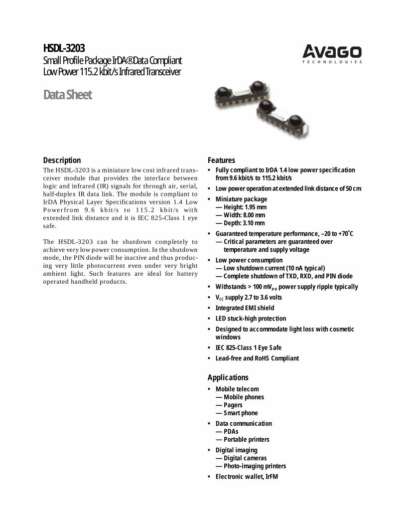
DescriptionThe HSDL-3203 is a miniature low cost infrared trans-ceiver module that provides the interface betweenlogic and infrared (IR) signals for through air, serial,half-duplex IR data link. The module is compliant toIrDA Physical Layer Specifications version 1.4 LowPowerfrom 9.6 kbit/s to 115.2 kbit/s withextended link distance and it is IEC 825-Class 1 eyesafe.
The HSDL-3203 can be shutdown completely toachieve very low power consumption. In the shutdownmode, the PIN diode will be inactive and thus produc-ing very little photocurrent even under very brightambient light. Such features are ideal for batteryoperated handheld products.
Features• Fully compliant to IrDA 1.4 low power specification
from 9.6 kbit/s to 115.2 kbit/s
• Low power operation at extended link distance of 50 cm
• Miniature package— Height: 1.95 mm— Width: 8.00 mm— Depth: 3.10 mm
• Guaranteed temperature performance, –20 to +70˚C— Critical parameters are guaranteed over
temperature and supply voltage
• Low power consumption— Low shutdown current (10 nA typical)— Complete shutdown of TXD, RXD, and PIN diode
• Withstands > 100 mVp-p power supply ripple typically
• VCC supply 2.7 to 3.6 volts
• Integrated EMI shield
• LED stuck-high protection
• Designed to accommodate light loss with cosmeticwindows
• IEC 825-Class 1 Eye Safe
• Lead-free and RoHS Compliant
Applications• Mobile telecom
— Mobile phones— Pagers— Smart phone
• Data communication— PDAs— Portable printers
• Digital imaging— Digital cameras— Photo-imaging printers
• Electronic wallet, IrFM
HSDL-3203Small Profile Package IrDA® Data CompliantLow Power 115.2 kbit/s Infrared Transceiver
Data Sheet

2
Figure 1. Functional block diagram of HSDL-3203.
Application SupportInformationThe Application Engineeringgroup in Avago Technologies isavailable to assist you with thetechnical understanding associ-ated with HSDL-3203 infraredtransceiver module. You can con-tact them through your localAvago sales representative foradditional details.
Figure 2. Rear view diagram with pin-out.
8 7 6 5 4 3 2 1
Ordering InformationPart Number Packaging Type Package QuantityHSDL-3203-021 Tape and Reel Front View 2500
7LED
DRIVER
6
5
RX PULSESHAPER
8
4
3
2
1
C2100 nF
SH
IEL
DC1
6.8 µF
TXD
LED A
GND
CX
RXD
VCC
SD
AGND
VCC
VCC
VCCR1

3
I/O Pin Configuration TablePin Symbol I/O Description Note1 CX I Pin bypass capacitor2 SD I Shutdown. Active high 13 AGND I Analog ground 24 GND I Ground 25 RXD O Receiver data output. Active low 36 VCC I Supply voltage 4
7 TXD I Transmitter data input. Active high 58 LED A I LED anode 6– Shield – EMI shield 7Notes:1. Complete shutdown TXD, RXD, and PIN diode.2. Connect to system ground.3. Output is active low pulse response when light pulse is seen.4. Regulated, 2.7 to 3.6 volt.5. Logic high turns on the LED. If held high longer than ∼ 50 µs, the LED is turned off
automatically. TXD must be driven either high or low. DO NOT leave the pin floating.6. Tied through external resistor, R1, to regulate VCC from 2.7 to 3.6 volt.7. Connect to system ground via a low inductance trace. For best performance, do not connect
to GND directly at the part.
Recommended Application Circuit ComponentsComponent Recommended Value NoteR1 30 Ω, ± 1%, 0.125 Watt 8R1 5.6 Ω, ± 1%, 0.125 Watt 9C1 6.8 µF, ± 20%, Tantalum 10C2 100 nF, ± 20%, X7R CeramicNotes:8. To obtain ILED of 50 mA for VLED of 3 V.9. To obtain ILED of 250 mA for VLED of 3 V.10. C1 must be placed within 0.7 cm of the HSDL-3203 to obtain optimum noise immunity.
Marking InformationThe unit is marked with theletters "A" and the datacode"YWW" on the shield for frontoptions where Y is the last digitof the year, and WW is theworkweek.
Transceiver I/O Truth TableInputs OutputsTXD Light Input to Receiver SD LED RXD NoteHigh Don't Care Low On Not ValidLow High Low Off Low 11, 12Low Low Low Off HighDon't Care Don't Care High Off HighNotes:11. In-band IrDA signals and data rates ≤ 115.2 kbit/s.12. RXD logic low is a pulsed response. The condition is maintained for a duration independent of pattern and strength of the incident intensity.
Caution: The BiCMOS inherent to the design of this component increases the component's susceptibilityto damage from electrostatic discharge (ESD). It is advised that normal static precautions be taken inhandling and assembly of this component to prevent damage and/or degradation, which may beinduced by ESD.

4
Recommended Operating ConditionsParameter Symbol Min. Max. Units Conditions NoteOperating Temperature TA –25 85 ˚CSupply Voltage VCC 2.7 3.6 VLogic High Voltage TXD, SD VIH 2/3 VCC VCC VLogic Low Voltage TXD, SD VIL 0 1/3 VCC VLogic High Receiver Input Irradiance EIH 0.0081 500 mW/cm2 For in-band signals 13Logic Low Receiver Input Irradiance EIL 0.3 µW/cm2 For in-band signals 13LED Current Pulse Amplitude ILEDA 50 250 mA Guaranteed at 25˚CReceiver Signal Rate 9.6 115.2 kbit/sNote:13. An in-band optical signal is a pulse/sequence where the peak wavelength, λp, is defined as 850 nm ≤ λp ≤ 900 nm, and the pulse characteristics
are compliant with the IrDA Serial Infrared Physical Layer Link Specification.
Absolute Maximum RatingsFor implementation where case to ambient thermal resistance is ≤ 50˚C/W.Parameter Symbol Min. Max. Units ConditionsStorage Temperature TS –40 100 ˚COperating Temperature TA –25 85 ˚CDC LED Current ILED (DC) 20 mAPeak LED Current ILED (PK) 250 mA ≤ 90 µs Pulse Width
≤ 25% Duty CycleLED Anode Voltage VLEDA –0.5 7 VSupply Voltage VCC 0 7 VInput Voltage TXD, SD VI 0 VCC + 0.5 VOutput Voltage RXD VO –0.5 VCC + 0.5 V

5
Electrical and Optical SpecificationsSpecifications hold over the recommended operating conditions unless otherwise noted. Unspecified test conditionscan be anywhere in their operating range. All typical values are at 25˚C and 3.0 V unless otherwise noted.Parameter Symbol Min. Typ. Max. Units Conditions NoteReceiverRXD Output Voltage Logic Low VOL 0 0.4 V IOL = 200 µA, for in-band EI 14
Logic High VOH VCC VCC V IOH = 200 µA, for in-band–0.2 EI ≤ 0.3 µW/cm2
Viewing Angle 2φ1/2 30 ˚Logic High Receiver Input EIH 0.0081 500 mW/cm2 For in-band signals ≤ 115.2 kbit/s 13IrradianceLogic Low Receiver Input EIL 0.3 µW/cm2 For in-band signals 13IrradiancePeak Sensitivity Wavelength λp 880 nmRXD Pulse Width tpw 1.5 2.5 4.0 µs 14RXD Rise and Fall Times tr, tf 25 100 ns tpw(EI) = 1.6 µs, CL = 10 pFReceiver Latency Time tL 25 50 µs 14Receiver Wake Up Time tW 50 100 µs 15TransmitterRadiant Intensity EIH 4 8 28.8 mW/sr ILEDA = 50 mA, TA = 25˚C,
θ1/2 ≤ 15˚22.5 mW/sr ILEDA = 250 mA, TA = 25˚C,
θ1/2 ≤ 15˚Peak Wavelength λp 875 nmSpectral Line Half Width ∆λ1/2 35 nmViewing Angle 2θ1/2 30 60 ˚Optical Pulse Width tpw 1.5 1.6 2 µs tpw(TXD) = 1.6 µsOptical Rise and Fall Times tr (EI) 600 ns tpw(TXD) = 1.6 µs
tf (EI)Maximum Optical Pulse Width tpw 20 50 µs TXD pin stuck high
(max)LED Anode ON State Voltage VON 1.5 V ILEDA = 50 mA,
(LEDA) VIH (TXD) = 2.7 VLED Anode OFF State Leakage ILK 0.01 1.0 µA VLEDA = VCC = 3.6 V,
(LEDA) VI (TXD) ≤ 1/3 VCC
TransceiverTXD and SD Input Logic Low IL –1 –0.01 1 µA 0 ≤ VI ≤ 1/3 VCC
Logic High IH 0.01 1 µA VI ≥ 2/3 VCC
Supply Current Shutdown ICCI 10 200 nA VCC = 3.6 V, VSD ≥ VCC –0.5Idle ICC2 2.5 4 mA VCC = 3.6 V, VI(TXD) ≤ 1/3 VCC,
EI = 0Active ICC3 2.6 5 mA VCC = 3.6 V, VI(TXD)≤ 1/3 VCC 16Receiver
Notes:14. For in-band signals ≤ 115.2 kbit/s where 8.1 µW/cm2 ≤ EI ≤ 500 mW/cm2.15. Wake up time is measured from SD pin HIGH to LOW transition or VCC power ON to valid RXD output.16. Typical value is at EI = 10 mW/cm2, maximum value is at EI = 500 mW/cm2.
Currents

6
Figure 3. RXD output waveform.
Figure 4. LED optical waveform.
Figure 5. TXD ‘Stuck On’ protection waveform.
Figure 6. Receiver wakeup time waveform. Figure 7. TXD wakeup time waveform.
tf
VOH90%
50%
10%VOL
tpw
tr
tf
LED OFF
90%
50%
10%
LED ON
tpw
tr
tpw (MAX.)
TXD
LED
RXLIGHT
tRW
RXD
SD
TXLIGHT
tTW
TXD
SD

7
Package Outline with Dimensions
Figure 8. LOP vs. ILED. Figure 9. VLED vs. LED current.
Figure 10. Package outline dimensions.
2.85
MOUNTINGCENTER 4.0
1.025
UNIT: mm
TOLERANCE: ± 0.2mm
CL
1.95
4.0
8.0
2.05
2.55
EMITTERRECEIVER
0.350.65
0.80
CL
3.325
P0.95 x 7 = 6.65
0.6
3.03.11.85
0.96
12345678
51 CX RXD62 SD VCC73 AGND TXD84 GND LEDA
COPLANARITY:± 0.1 mm
RA
DIA
NT
INT
EN
SIT
Y (
mW
/sr)
40
ILED_A (A)
15
100.0E-30
5
000.0E+0 300.0E-3
25
30
20
10
RADIANT INTENSITY vs ILED_A,TEMPERATURE = 25°C
35
200.0E-3
VL
ED
_A (
V)
2.2
ILED_A (A)
1.4
100.0E-31.0000.0E+0 300.0E-3
1.8
1.6
1.2
VLED_A vs ILED_A,TEMPERATURE = 25°C
2.0
200.0E-3

8
Tape and Reel Dimensions
Figure 11. Tape and reel dimensions.
16.4 + 2 0
21 ± 0.8
UNIT: mm
B C
∅ 13.0 ± 0.5
2.0 ± 0.5
2.0 ± 0.5
LABEL
3.4 ± 0.1
8.4 ± 0.1
8.0 ± 0.1
4.0 ± 0.1
1.5 ± 0.1
7.5 ± 0.116.0 ± 0.2
1.75 ± 0.1
∅ 1.5+ 0.1 0
0.4 ± 0.05
2.8 ± 0.1
POLARITY
PIN 8: LED A
PIN 1: CX
OPTION # "B" "C" QUANTITY
001
021
178
330
60
80
500
2500
EMPTY PARTS MOUNTED LEADER
EMPTY
(40 mm MIN.) (400 mm MIN.)
(40 mm MIN.)
PROGRESSIVE DIRECTION
R 1.0
DETAIL A
DETAIL A
UNIT: mm

9
Moisture-Proof PackagingAll HSDL-3203 options are shipped in moisture-proof packaging. Once opened, moisture absorption begins.
Recommended StorageConditionsStorage Temp. 10˚C to 30˚CRelative Humidity Below 60% RH
Time from Unsealing to SolderingAfter removal from the bag, theparts should be soldered withintwo days if stored at the recom-mended storage conditions. Iftimes longer than two days areneeded, the parts must be storedin a dry box.
Figure 12. Baking conditions chart.
Baking ConditionsIf the parts are not stored in dryconditions, they must be bakedbefore reflow to prevent damageto the parts.
Packaging Temp. TimeIn Reels 60˚C ≥ 48 hoursIn Bulk 100˚C ≥ 4 hours
125˚C ≥ 2 hours150˚C ≥ 1 hour
Baking should only be done once.
UNITS IN A SEALEDMOISTURE-PROOF
PACKAGE
PACKAGE ISOPENED (UNSEALED)
ENVIRONMENTLESS THAN 25°C,AND LESS THAN
60% RH?
PACKAGE ISOPENED MORETHAN 2 DAYS?
PERFORM RECOMMENDEDBAKING CONDITIONS
NO BAKINGIS NECESSARY
YES
NO
YES
NO

10
Reflow Profile
Process Zone Symbol ∆T Maximum ∆T/∆timeHeat Up P1, R1 25˚C to 160˚C 4˚C/sSolder Paste Dry P2, R2 160˚C to 200˚C 0.5˚C/sSolder Reflow P3, R3 200˚C to 255˚C (260˚C at 10 seconds max.) 4˚C/s
P3, R4 255˚C to 200˚C –6˚C/sCool Down P4, R5 200˚C to 25˚C –6˚C/s
Figure 13. Reflow graph.
The reflow profile is a straightline representation of a nominaltemperature profile for a convec-tive reflow solder process. Thetemperature profile is dividedinto four process zones, eachwith different ∆T/∆time tempera-ture change rates. The ∆T/∆timerates are detailed in the abovetable. The temperatures aremeasured at the component toprinted circuit board connections.
In process zone P1, the PC boardand HSDL-3203 castellation I/Opins are heated to a temperatureof 160°C to activate the flux inthe solder paste. The temperatureramp up rate, R1, is limited to4°C per second to allow for evenheating of both the PC board andHSDL-3203 castellation I/O pins.
Process zone P2 should be ofsufficient time duration (60 to120 seconds) to dry the solderpaste. The temperature is raisedto a level just below the liquiduspoint of the solder, usually 200°C(392°F).
Process zone P3 is the solderreflow zone. In zone P3, the tem-perature is quickly raised abovethe liquidus point of solder to255°C (491°F) for optimumresults. The dwell time above theliquidus point of solder should bebetween 20 and 60 seconds. Itusually takes about 20 seconds toassure proper coalescing of thesolder balls into liquid solder andthe formation of good solderconnections. Beyond a dwelltime of 60 seconds, the inter-
metallic growth within the solderconnections becomes excessive,resulting in the formation of weakand unreliable connections. Thetemperature is then rapidlyreduced to a point below thesolidus temperature of the solder,usually 200°C (392°F), to allowthe solder within the connectionsto freeze solid.
Process zone P4 is the cool downafter solder freeze. The cooldown rate, R5, from the liquiduspoint of the solder to 25°C (77°F)should not exceed 6°C per secondmaximum. This limitation is nec-essary to allow the PC board andHSDL-3203 castellation I/O pinsto change dimensions evenly,putting minimal stresses on theHSDL-3203 transceiver.
0
t-TIME (SECONDS)
T –
TEM
PER
ATU
RE
– (°
C)
230
200
160
120
80
50 150100 200 250 300
180
220
255
P1HEAT
UP
P2SOLDER PASTE DRY
P3SOLDERREFLOW
P4COOL
DOWN
25
R1
R2
R3 R4
R5
60 sec. MAX.
ABOVE220°C
MAX. 260°C

11
Figure 14. Stencil and PCBA.
1.1 Recommended Land Pattern
Appendix A : SMT Assembly Application Note
1.0 Solder Pad, Mask and Metal Solder Stencil Aperture
Figure 15. Land pattern.
METAL STENCILFOR SOLDER PASTEPRINTING
LANDPATTERN
PCBA
STENCILAPERTURE
SOLDERMASK
0.60
1.25
1.75
1.35
0.10
0.4751.425
2.375
3.325
CL
MOUNTINGCENTER
SHIELDSOLDER PAD
FIDUCIAL
2.05
0.775
UNIT: mm

12
Figure 17. Adjacent land keep-out and solder mask areas.
Stencil Thickness, t (mm) Aperture Size (mm)Length, l Width, w
0.152 mm 2.60 ± 0.05 0.55 ± 0.050.127 mm 3.00 ± 0.05 0.55 ± 0.05
Figure 16. Solder stencil aperture.
1.2 Recommended Metal SolderStencil ApertureIt is recommended that only a0.152 mm (0.006 inches) or a0.127 mm (0.005 inches) thickstencil be used for solder pasteprinting. This is to ensure ad-equate printed solder paste vol-ume and no shorting. See thetable below the drawing for com-binations of metal stencil aper-ture and metal stencil thicknessthat should be used.
Aperture opening for shield padis 2.7 mm x 1.25 mm as per landpattern.
1.3 Adjacent Land Keepout andSolder Mask AreasAdjacent land keep-out is themaximum space occupied bythe unit relative to the land pat-tern. There should be no otherSMD components within thisarea.
The minimum solder resist stripwidth required to avoid solderbridging adjacent pads is0.2 mm. It is recommended thattwo fiducial crosses be placed atmid-length of the pads for unitalignment.
Note: Wet/Liquid Photo-Imageable solder resist/mask isrecommended.
APERTURES AS PERLAND DIMENSIONS
lw
t
0.2
3.0
8.2
SOLDER MASK
2.6
UNITS: mm

13
Appendix B: PCB LayoutSuggestionThe following shows an exampleof a PCB layout using option#021 that would result in goodelectrical and EMI performance.Things to note:
1. The ground plane should becontinuous under the part, butshould not extend under theshield trace.
2. The shield trace is a wide, lowinductance trace back to thesystem ground.
3. The AGND pin is connected tothe ground plane and not tothe shield tab.
4. C1 and C3 are optional supplyfilter capacitors; they may beleft out if a clean power sup-ply is used.
5. VLED can be connected toeither unfiltered or unregu-lated power supply. If VLEDand VCC share the same powersupply and C1 is used, theconnection should be beforethe C1 cap. In a noisy envi-ronment, supply rejection canbe enhanced by including C3as well.
Figure 18. PCB layout suggestions.
VL
ED
TX
D
RX
D
SH
UT
DO
WN
VC
C
SH
IEL
D
SY
ST
EM
GR
OU
ND
C2
C3
C1R1
COMPONENT SIDE
CIRCUIT SIDE

14
Appendix C: General ApplicationGuide for the HSDL-3203 InfraredIrDA® Compliant 115.2 kb/sTransceiverDescriptionThe HSDL-3203, a wide voltageoperating range infraredtransceiver, is a low-cost andsmall form factor device that isdesigned to address the mobilecomputing market such as PDAs,as well as small embedded mobileproducts such as digital camerasand cellular phones. It is fullycompliant to IrDA 1.4 low powerspecification from 9.6 kb/s to115.2 kb/s, and supports HP-SIRand TV Remote modes. Thedesign of the HSDL-3203 alsoincludes the following uniquefeatures:• Low passive component count.• Shutdown mode for low power
consumption requirement.
Interface to Recommended I/O ChipsThe HSDL-3203’s TXD data inputis buffered to allow for CMOSdrive levels. No peaking circuit orcapacitor is required.
Data rate from 9.6 kb/s up to115.2 kb/s is available at the RXDpin.
The block diagram below showsow the IR port fits into a mobilephone and PDA platform.
Recommended VCC Intensity Minimum peakR1 pulse LED current30 Ω 3 V 8 mW/sr 50 mA5.6 Ω 3 V 34 mW/sr 250 mA
Selection of Resistor R1Resistor R1 should be selected toprovide the appropriate peakpulse LED current over differentranges of VCC as shown in thetable below.
TRANSCEIVERMOD/
DE-MODULATOR
SPEAKER
RF INTERFACE
AUDIO INTERFACE
USER INTERFACE
MICROCONTROLLER
DSP CORE
ASICCONTROLLER
IR
MICROPHONE
MOBILE PHONE PLATFORM HSDL-3203
Figure 19. IR layout in mobile phone platform.

15
Figure 20. IR layout in PDA platform.
The link distance testing wasdone using typical HSDL-3203units with NationalSemiconductor’s PC87109 3VSuper I/O controller and SMC’sFDC37C669 and FDC37N769Super I/O controllers. An IR linkdistance of up to 100 cm wasdemonstrated.
PCMCIACONTROLLER
CPUFOR EMBEDDED
APPLICATION
IR
HSDL-3203
RAM
ROM
TOUCHPANEL
LCDPANEL
RS232CDRIVER
COMPORT
PDA PLATFORM

16
Appendix D: Optical portdimensions for HSDL-3203:To ensure IrDA compliance, someconstraints on the height andwidth of the window exist. Theminimum dimensions ensure thatthe IrDA cone angles are metwithout vignetting. The maximumdimensions minimize the effectsof stray light. The minimum sizecorresponds to a cone angle of30˚ and the maximum size corre-sponds to a cone angle of 60˚.
In the figure below, X is the widthof the window, Y is the height ofthe window, and Z is the distance
from the HSDL-3203 to the backof the window. The distance fromthe center of the LED lens to thecenter of the photodiode lens, K,is 5.1 mm. The equations forcomputing the window dimen-sions are as follows:
X = K + 2*(Z + D)*tanAY = 2*(Z + D)*tanA
The above equations assume thatthe thickness of the window isnegligible compared to the dis-tance of the module from theback of the window (Z). If theyare comparable, Z' replaces Z in
the above equation. Z' is definedas:
Z' = Z + t/n
where ‘t’ is the thickness of thewindow and ‘n’ is the refractiveindex of the window material.
The depth of the LED image in-side the HSDL-3203, D, is3.17 mm. ‘A’ is the required halfangle for viewing. For IrDA com-pliance, the minimum is 15˚ andthe maximum is 30˚. Assumingthe thickness of the window to benegligible, the equations result inthe following tables and graphs.
D
Z
K
A
IR TRANSPARENTWINDOW
OPAQUEMATERIAL
OPAQUEMATERIAL
IR TRANSPARENT WINDOW
X
Z

17
AP
ER
TU
RE
WID
TH
(X
) –
mm
25
MODULE DEPTH (Z) – mm
10
4 70
0 9
15
2 6
20
5
1 3 5 8
APERTURE WIDTH (X) vs MODULE DEPTH
X MAX.X MIN.
AP
ER
TU
RE
HE
IGH
T (
Y)
– m
m
16
MODULE DEPTH (Z) – mm
8
4 70
0 9
10
2 6
4
1 3 5 8
APERTURE HEIGHT (Y) vs MODULE DEPTH
14
12
6
2Y MAX.Y MIN.
Module Depth Aperture Width (x, mm) Aperture Height (y, mm)(z) mm Max. Min. Max. Min.0 8.76 6.80 3.66 1.701 9.92 7.33 4.82 2.332 11.07 7.87 5.97 2.773 12.22 8.41 7.12 3.314 13.38 8.94 8.28 3.845 14.53 9.48 9.43 4.386 15.69 10.01 10.59 4.917 16.84 10.55 11.74 5.458 18.00 11.09 12.90 5.999 19.15 11.62 14.05 6.52

Curved Front and Back(Second Choice)
Flat Window(First Choice)
Curved Front, Flat Back(Do Not Use)
Shape of the WindowFrom an optics standpoint, thewindow should be flat. This en-sures that the window will notalter either the radiation patternof the LED, or the receive patternof the photodiode.
If the window must be curved formechanical or industrial designreasons, place the same curve onthe back side of the window thathas an identical radius as thefront side. While this will notcompletely eliminate the lenseffect of the front curved surface,it will significantly reduce theeffects. The amount of change in
the radiation pattern is dependentupon the material chosen for thewindow, the radius of the frontand back curves, and the distancefrom the back surface to thetransceiver. Once these items areknown, a lens design can bemade which will eliminate theeffect of the front surface curve.
The following drawings show theeffects of a curved window on theradiation pattern. In all cases,the center thickness of the win-dow is 1.5 mm, the window ismade of polycarbonate plastic,and the distance from the trans-ceiver to the back surface of thewindow is 3 mm.
Window MaterialAlmost any plastic material willwork as a window material. Poly-carbonate is recommended. Thesurface finish of the plasticshould be smooth, without anytexture. An IR filter dye may beused in the window to make itlook black to the eye, but thetotal optical loss of the windowshould be 10% or less for bestoptical performance. Light lossshould be measured at 875 nm.
The recommended plasticmaterials for use as a cosmeticwindow are available fromGeneral Electric Plastics.Recommended Plastic Materials:
Material Light RefractiveNumber Transmission Haze IndexLexan 141L 88% 1% 1.586Lexan 920A 85% 1% 1.586Lexan 940A 85% 1% 1.586Note: 920A and 940A are more flame retardant than 141L.Recommended Dye: Violet #21051 (IR transmissant above625 nm).
18

For product information and a complete list of distributors, please go to our website: www.avagotech.com
Avago, Avago Technologies, and the A logo are trademarks of Avago Technologies, Limited in the United States and other countries.Data subject to change. Copyright © 2006 Avago Technologies Pte. All rights reserved. Obsoletes 5988-8581EN5989-2869EN May 28, 2006