Embed Size (px)
Citation preview

DATA -PARALLEL DIGITAL SIGNAL
PROCESSORS: A LGORITHM M APPING ,ARCHITECTURE SCALING AND
WORKLOAD ADAPTATION
Sridhar Rajagopal
Thesis: Doctor of PhilosophyElectrical and Computer EngineeringRice University, Houston, Texas (May 2004)

RICE UNIVERSITY
Data-parallel Digital Signal Processors: AlgorithmMapping, Architecture Scaling and Workload Adaptation
by
Sridhar Rajagopal
A THESISSUBMITTED
IN PARTIAL FULFILLMENT OF THE
REQUIREMENTS FOR THEDEGREE
Doctor of Philosophy
APPROVED, THESIS COMMITTEE:
Joseph R. Cavallaro, ChairProfessor of Electrical and ComputerEngineering and Computer Science
Scott RixnerAssistant Professor of Computer Science andElectrical and Computer Engineering
Behnaam AazhangJ.S.Abercrombie Professor of Electrical andComputer Engineering
David B. JohnsonAssociate Professor of Computer Scienceand Electrical and Computer Engineering
Houston, Texas
May, 2004

ABSTRACT
Data-parallel Digital Signal Processors: Algorithm Mapping, Architecture Scaling and
Workload Adaptation
by
Sridhar Rajagopal
Emerging applications such as high definition television (HDTV), streaming video, im-
age processing in embedded applications and signal processing in high-speed wireless com-
munications are driving a need for high performance digitalsignal processors (DSPs) with
real-time processing. This class of applications demonstrates significant data parallelism,
finite precision, need for power-efficiency and the need for 100’s of arithmetic units in
the DSP to meet real-time requirements. Data-parallel DSPsmeet these requirements by
employing clusters of functional units, enabling 100’s of computations every clock cycle.
These DSPs exploit instruction level parallelism and subword parallelism within clusters,
similar to a traditional VLIW (Very Long Instruction Word) DSP, and exploit data paral-
lelism across clusters, similar to vector processors.
Stream processors are data-parallel DSPs that use a bandwidth hierarchy to support
dataflow to 100’s of arithmetic units and are used for evaluating the contributions of this
thesis. Different software realizations of the dataflow in the algorithms can affect the per-
formance of stream processors by greater than an order-of-magnitude. The thesis first
presents the design of signal processing algorithms that map efficiently on stream proces-
sors by parallelizing the algorithms and by re-ordering theflow of data. The design space
for stream processors also exhibits trade-offs between arithmetic units per cluster, clusters

and the clock frequency to meet the real-time requirements of a given application. This
thesis provides a design space exploration tool for stream processors that meets real-time
requirements while minimizing power consumption. The presented exploration method-
ology rapidly searches this design space at compile time to minimize power consumption
and selects the number of adders, multipliers, clusters andthe real-time clock frequency
in the processor. Finally, the thesis improves the power efficiency in the designed stream
processor by adapting the compute resources to run-time variations in the workload. The
thesis presents an adaptive multiplexer network that allows the number of active clusters
to be varied during run-time by turning off unused clusters.Thus, by efficient mapping of
algorithms, exploring the architecture design space, and by compute resource adaptation,
this thesis improves power efficiency in stream processors and enhances their suitability for
high performance, power-aware, signal processing applications.

Acknowledgments
I would like to thank my advisor, Dr. Joseph Cavallaro, for his time, guidance and financial
support throughout my education at Rice. He has probably devoted more of his time,
energy and patience with me than any of his other students. Hehas financially supported
me throughout my education with funds ranging into hundredsof thousands of dollars
over the last 6 years, enabled me to get internships at Nokia in Oulu, Finland and in Nokia
Research Center, Dallas and travel to numerous conferences. I am extremely grateful to Dr.
Scott Rixner for being on my thesis committee. My thesis builds on his research on stream
processors and Dr. Rixner provided me with the tools, the infrastructure, and support
necessary for my thesis. I have benefited immensely from his advice and positive criticism
while working with him over the last three years. I am also grateful to Dr. Behnaam
Aazhang for all the advice and care he has imparted on me over the entire duration of
my thesis. I have always felt that he treated me as one of his own students and have
benefited from his advice on both technical and non-technical matters. I also thank Dr.
David Johnson for being on my committee and providing me withfeedback. I have always
enjoyed conversing with him in his office for long hours on varying topics. It has been a
pleasure to have four established professors in different disciplines on my thesis committee
who were actively interested in my research and provided me with guidance and feedback.
I have also enjoyed interacting with several other faculty in the department, including
Dr. Ashutosh Sabharwal, Dr. Michael Orchard, Dr. Vijay Pai,Dr. Yehia Massoud and
Dr. Kartik Mohanram, who have provided me with comments and feedback on my work at
various stages of my thesis. I have also been delighted to have great friends at Rice during
my stay there, including Kiran, Ravi, Marjan, Mahsa, Predrag, Abha, Amit, Dhruv, Vinod,
Alex, Karthick, Suman, Mahesh, Martin, Partha, Vinay, Violeta and so many others. I am

v
also grateful to Dr. Tracy Volz and Dr. Jan Hewitt for their help with presentations and
thesis writing during the course of my education at Rice. I amalso grateful to the Office of
International Students at Rice and especially, Dr. Adria Baker, for making my international
study experience at Rice a wonderful and memorable experience.
I am grateful to the Imagine stream processor research groupat Stanford for their timely
help and support with their tools, especially Ujval, Brucekand Abhishek. I am also grateful
to researchers from Nokia and Texas Instruments for their comments and discussions that
we had over the last five years: Dr. Anand Kannan, Dr. Anand Dabak, Gang Xu, Dr.
Giridhar Mandyam, Dr. Jorma Lilleberg, Dr. Alan Gatherer, Dennis McCain. I have
significantly benefited from the meetings, interactions andadvice. Finally, I would like to
thank my parents for allowing me to embark on this journey andsupporting me through
this time. This journey has transformed me from a boy to a man.
My graduate education has been supported in part by Nokia, Texas Instruments, the
Texas Advanced Technology Program under grant 1999-003604-080, by NSF under grants
NCR-9506681 and ANI-9979465, a Rice University Fellowshipand a Nokia Fellowship.

Contents
Abstract ii
Acknowledgments iv
List of Illustrations xi
List of Tables xv
1 Introduction 1
1.1 Data-parallel Digital Signal Processors . . . . . . . . . . . .. . . . . . . . 1
1.2 Design challenges for data-parallel DSPs . . . . . . . . . . . .. . . . . . . 5
1.2.1 Definition of programmable DSPs . . . . . . . . . . . . . . . . . . 5
1.2.2 Algorithm mapping and tools for data-parallel DSPs . .. . . . . . 5
1.2.3 Comparing data-parallel DSPs with other architectures . . . . . . . 6
1.3 Hypothesis . . . . . . . . . . . . . . . . . . . . . . . . . . . . . . . . . . 7
1.4 Contributions . . . . . . . . . . . . . . . . . . . . . . . . . . . . . . . . . 8
1.5 Thesis Overview . . . . . . . . . . . . . . . . . . . . . . . . . . . . . . . 10
2 Algorithms for stream processors: Cellular base-stations 11
2.1 Baseband processing . . . . . . . . . . . . . . . . . . . . . . . . . . . . . 11
2.2 2G CDMA Base-station . . . . . . . . . . . . . . . . . . . . . . . . . . . . 14
2.2.1 Received signal model . . . . . . . . . . . . . . . . . . . . . . . . 17
2.3 3G CDMA Base-station . . . . . . . . . . . . . . . . . . . . . . . . . . . . 19
2.3.1 Iterative scheme for channel estimation . . . . . . . . . . .. . . . 22
2.3.2 Multiuser detection . . . . . . . . . . . . . . . . . . . . . . . . . . 24
2.4 4G CDMA Base-station . . . . . . . . . . . . . . . . . . . . . . . . . . . . 27
2.4.1 System Model . . . . . . . . . . . . . . . . . . . . . . . . . . . . 28

vii
2.4.2 Chip level MIMO equalization . . . . . . . . . . . . . . . . . . . . 31
2.4.3 LDPC decoding . . . . . . . . . . . . . . . . . . . . . . . . . . . . 33
2.4.4 Memory and operation count requirements . . . . . . . . . . .. . 37
2.5 Summary . . . . . . . . . . . . . . . . . . . . . . . . . . . . . . . . . . . 37
3 High performance DSP architectures 39
3.1 Traditional solutions for real-time processing . . . . . .. . . . . . . . . . 39
3.2 Limitations of single processor DSP architectures . . . .. . . . . . . . . . 41
3.3 Programmable multiprocessor DSP architectures . . . . . .. . . . . . . . 42
3.3.1 Multi-chip MIMD processors . . . . . . . . . . . . . . . . . . . . 43
3.3.2 Single-chip MIMD processors . . . . . . . . . . . . . . . . . . . . 44
3.3.3 SIMD array processors . . . . . . . . . . . . . . . . . . . . . . . . 45
3.3.4 SIMD vector processors . . . . . . . . . . . . . . . . . . . . . . . 46
3.3.5 Data-parallel DSPs . . . . . . . . . . . . . . . . . . . . . . . . . . 46
3.3.6 Pipelining multiple processors . . . . . . . . . . . . . . . . . .. . 47
3.4 Reconfigurable architectures . . . . . . . . . . . . . . . . . . . . . .. . . 48
3.5 Issues in choosing a multiprocessor architecture for evaluation . . . . . . . 49
3.6 Summary . . . . . . . . . . . . . . . . . . . . . . . . . . . . . . . . . . . 50
4 Stream processors 52
4.1 Introduction . . . . . . . . . . . . . . . . . . . . . . . . . . . . . . . . . . 52
4.2 Programming model of the Imagine stream processor . . . . .. . . . . . . 55
4.3 The Imagine stream processor simulator . . . . . . . . . . . . . .. . . . . 57
4.3.1 Programming complexity . . . . . . . . . . . . . . . . . . . . . . . 61
4.4 Architectural improvements for power-efficient streamprocessors . . . . . 63
4.5 Summary . . . . . . . . . . . . . . . . . . . . . . . . . . . . . . . . . . . 64
5 Mapping algorithms on stream processors 66
5.1 Related work on benchmarking stream processors . . . . . . .. . . . . . . 66

viii
5.2 Stream processor mapping and characteristics . . . . . . . .. . . . . . . . 68
5.3 Algorithm benchmarks for mapping: wireless communications . . . . . . . 71
5.3.1 Matrix transpose . . . . . . . . . . . . . . . . . . . . . . . . . . . 71
5.3.2 Matrix outer products . . . . . . . . . . . . . . . . . . . . . . . . . 73
5.3.3 Matrix-vector multiplication . . . . . . . . . . . . . . . . . . .. . 75
5.3.4 Matrix-matrix multiplication . . . . . . . . . . . . . . . . . . .. . 78
5.3.5 Viterbi decoding . . . . . . . . . . . . . . . . . . . . . . . . . . . 80
5.3.6 LDPC decoding . . . . . . . . . . . . . . . . . . . . . . . . . . . . 84
5.3.7 Turbo decoding . . . . . . . . . . . . . . . . . . . . . . . . . . . . 84
5.4 Tradeoffs between subword parallelism and inter-cluster communication . . 86
5.5 Tradeoffs between data reordering in memory and arithmetic clusters . . . . 88
5.5.1 Memory stalls and functional unit utilization . . . . . .. . . . . . 90
5.6 Inter-cluster communication patterns in wireless systems . . . . . . . . . . 91
5.7 Stream processor performance for 2G,3G,4G systems . . . .. . . . . . . . 92
5.8 Summary . . . . . . . . . . . . . . . . . . . . . . . . . . . . . . . . . . . 95
6 Design space exploration for stream processors 96
6.1 Motivation . . . . . . . . . . . . . . . . . . . . . . . . . . . . . . . . . . . 96
6.1.1 Related work . . . . . . . . . . . . . . . . . . . . . . . . . . . . . 98
6.2 Design exploration framework . . . . . . . . . . . . . . . . . . . . . .. . 98
6.2.1 Mathematical modeling . . . . . . . . . . . . . . . . . . . . . . . 102
6.2.2 Capacitance model for stream processors . . . . . . . . . . .. . . 105
6.2.3 Sensitivity analysis . . . . . . . . . . . . . . . . . . . . . . . . . . 108
6.3 Design space exploration . . . . . . . . . . . . . . . . . . . . . . . . . .. 110
6.3.1 Setting the number of clusters . . . . . . . . . . . . . . . . . . . .111
6.3.2 Setting the number of ALUs per cluster . . . . . . . . . . . . . .. 112
6.3.3 Relation between power minimization and functional unit efficiency 112
6.4 Results . . . . . . . . . . . . . . . . . . . . . . . . . . . . . . . . . . . . . 114

ix
6.4.1 Verifications with detailed simulations . . . . . . . . . . .. . . . . 122
6.4.2 2G-3G-4G exploration . . . . . . . . . . . . . . . . . . . . . . . . 123
6.5 Summary . . . . . . . . . . . . . . . . . . . . . . . . . . . . . . . . . . . 125
7 Improving power efficiency in stream processors 127
7.1 Need for reconfiguration . . . . . . . . . . . . . . . . . . . . . . . . . . .127
7.2 Methods of reconfiguration . . . . . . . . . . . . . . . . . . . . . . . . .. 128
7.2.1 Reconfiguration in memory . . . . . . . . . . . . . . . . . . . . . 128
7.2.2 Reconfiguration using conditional streams . . . . . . . . .. . . . . 131
7.2.3 Reconfiguration using adaptive stream buffers . . . . . .. . . . . . 132
7.3 Imagine simulator modifications . . . . . . . . . . . . . . . . . . . .. . . 136
7.3.1 Impact of power gating and voltage scaling . . . . . . . . . .. . . 138
7.4 Power model . . . . . . . . . . . . . . . . . . . . . . . . . . . . . . . . . 139
7.4.1 Cluster arrangement for low power . . . . . . . . . . . . . . . . .141
7.5 Results . . . . . . . . . . . . . . . . . . . . . . . . . . . . . . . . . . . . . 142
7.5.1 Comparisons between reconfiguration methods . . . . . . .. . . . 142
7.5.2 Voltage-Frequency Scaling . . . . . . . . . . . . . . . . . . . . . .144
7.5.3 Comparing DSP power numbers . . . . . . . . . . . . . . . . . . . 149
7.5.4 Comparisons with ASIC based solutions . . . . . . . . . . . . .. . 150
7.6 Summary . . . . . . . . . . . . . . . . . . . . . . . . . . . . . . . . . . . 152
8 Conclusions and Future Work 153
8.1 Conclusions . . . . . . . . . . . . . . . . . . . . . . . . . . . . . . . . . . 153
8.2 Future work . . . . . . . . . . . . . . . . . . . . . . . . . . . . . . . . . . 154
8.2.1 MAC layer integration on the host processor . . . . . . . . .. . . 154
8.2.2 Power analysis . . . . . . . . . . . . . . . . . . . . . . . . . . . . 154
8.2.3 Pipelined, Multi-threaded and reconfigurable processors . . . . . . 155
8.2.4 LDPC and Turbo decoding . . . . . . . . . . . . . . . . . . . . . . 155
8.3 Need for new definitions, workloads and architectures . .. . . . . . . . . . 156

x
A Tools and Applications for distribution 158
A.1 Design exploration support . . . . . . . . . . . . . . . . . . . . . . . .. . 158
A.2 Reconfiguration support for power efficiency . . . . . . . . . .. . . . . . 158
A.3 Applications . . . . . . . . . . . . . . . . . . . . . . . . . . . . . . . . . . 159
Bibliography 160

Illustrations
1.1 Trends in wireless data rates and clock frequencies (Sources: Intel, IEEE
802.11b, IEEE 802.11a, W-CDMA) . . . . . . . . . . . . . . . . . . . . . 3
2.1 Base-station transmitter (after Texas Instruments [1]) . . . . . . . . . . . . 12
2.2 Base-station receiver (after Texas Instruments [1]) . .. . . . . . . . . . . . 13
2.3 Algorithms considered for a 2G base-station . . . . . . . . . .. . . . . . . 16
2.4 Operation count break-up for a 2G base-station . . . . . . . .. . . . . . . 20
2.5 Memory requirements of a 2G base-station . . . . . . . . . . . . .. . . . . 20
2.6 Algorithms considered for a 3G base-station . . . . . . . . . .. . . . . . . 21
2.7 Operation count break-up for a 3G base-station . . . . . . . .. . . . . . . 27
2.8 Memory requirements of a 3G base-station . . . . . . . . . . . . .. . . . . 28
2.9 MIMO system model . . . . . . . . . . . . . . . . . . . . . . . . . . . . . 29
2.10 Algorithms considered for a 4G base-station . . . . . . . . .. . . . . . . . 30
2.11 LDPC decoding . . . . . . . . . . . . . . . . . . . . . . . . . . . . . . . . 35
2.12 Operation count break-up for a 4G base-station . . . . . . .. . . . . . . . 37
2.13 Memory requirements of a 4G base-station . . . . . . . . . . . .. . . . . . 38
3.1 Traditional base-station architecture designs [2–5] .. . . . . . . . . . . . . 40
3.2 Register file explosion in traditional DSPs with centralized register files.
Courtesy: Scott Rixner . . . . . . . . . . . . . . . . . . . . . . . . . . . . 42
3.3 Multiprocessor classification . . . . . . . . . . . . . . . . . . . . .. . . . 51

xii
4.1 Parallelism levels in DSPs and stream processors . . . . . .. . . . . . . . 53
4.2 A Traditional Stream Processor . . . . . . . . . . . . . . . . . . . . .. . . 54
4.3 Internal details of a stream processor cluster, adaptedfrom Scott Rixner [6] 56
4.4 Programming model . . . . . . . . . . . . . . . . . . . . . . . . . . . . . 57
4.5 Stream processor programming example(a) is regular code ; (b) is stream
+ kernel code . . . . . . . . . . . . . . . . . . . . . . . . . . . . . . . . . 58
4.6 The Imagine stream processor simulator programming model . . . . . . . . 59
4.7 The schedule visualizer provides insights on the schedule and the
dependencies . . . . . . . . . . . . . . . . . . . . . . . . . . . . . . . . . 60
4.8 The schedule visualizer also provides insights on memory stalls . . . . . . 61
4.9 Architecture space for stream processors . . . . . . . . . . . .. . . . . . . 64
4.10 Architectural improvements for power savings in stream processors . . . . 65
5.1 Estimation, detection, decoding from a programmable architecture
mapping perspective . . . . . . . . . . . . . . . . . . . . . . . . . . . . . 68
5.2 Matrix transpose in data parallel architectures using the Altivec approach . 72
5.3 A 4�4 matrix transpose on a 4-cluster processor . . . . . . . . . . . . . .73
5.4 32x32 matrix transpose with increasing clusters . . . . . .. . . . . . . . . 74
5.5 ALU utilization variation with adders and multipliers for 32x32 matrix
transpose . . . . . . . . . . . . . . . . . . . . . . . . . . . . . . . . . . . 74
5.6 Performance of a 32-length vector outer product resulting in a 32x32
matrix with increasing clusters . . . . . . . . . . . . . . . . . . . . . . .. 75
5.7 ALU utilization variation with adders and multipliers for 32-vector outer
product . . . . . . . . . . . . . . . . . . . . . . . . . . . . . . . . . . . . 76
5.8 Matrix-vector multiplication in data parallel architectures . . . . . . . . . . 77
5.9 Performance of a 32x32 matrix-vector multiplication with increasing clusters 78
5.10 Performance of a 32x32 matrix-matrix multiplication with increasing
clusters . . . . . . . . . . . . . . . . . . . . . . . . . . . . . . . . . . . . 79

xiii
5.11 Viterbi trellis shuffling for data parallel architectures . . . . . . . . . . . . 81
5.12 Viterbi decoding using register-exchange [7] . . . . . . .. . . . . . . . . . 82
5.13 Viterbi decoding performance for 32 users for varying constraint lengths
and clusters . . . . . . . . . . . . . . . . . . . . . . . . . . . . . . . . . . 83
5.14 ALU utilization for ’Add-Compare-Select’ kernel in Viterbi decoding . . . 83
5.15 Bit and check node access pattern for LDPC decoding . . . .. . . . . . . . 85
5.16 Example to demonstrate trade-offs between subword parallelism
utilization (packing) and inter-cluster communication instream processors . 87
5.17 Example to demonstrate trade-offs between data reordering in memory
and arithmetic clusters in stream processors . . . . . . . . . . . .. . . . . 89
5.18 Matrix transpose in memory vs. arithmetic clusters fora 32-cluster stream
processor . . . . . . . . . . . . . . . . . . . . . . . . . . . . . . . . . . . 90
5.19 A reduced inter-cluster communication network with only nearest
neighbor connections for odd-even grouping . . . . . . . . . . . . .. . . . 93
5.20 Real-time performance of stream processors for 2G and 3G fully loaded
base-stations . . . . . . . . . . . . . . . . . . . . . . . . . . . . . . . . . . 94
6.1 Breakdown of the real-time frequency (execution time) of a workload . . . 100
6.2 Viterbi decoding performance for varying constraint lengths and clusters . . 102
6.3 Design exploration framework for embedded stream processors . . . . . . . 104
6.4 Variation of real-time frequency with increasing clusters . . . . . . . . . . 115
6.5 Minimum power point with increasing clusters and variations in� and� .
The thin lines show the variation with� . (���� ,����) = (5,3) . . . . . . . . 117
6.6 Real-time frequency variation with varying adders and multipliers for� � , � � � � �, � = 1,� � �, refining on the�� � � � �� � �� � � � � solution118
6.7 Sensitivity of power minimization to� , � and� for clusters . . . . . . . 120
6.8 Variation of cluster utilization with cluster index . . .. . . . . . . . . . . . 121

xiv
6.9 Verification of design tool output (T) with a detailed cycle-accurate
simulation (S) . . . . . . . . . . . . . . . . . . . . . . . . . . . . . . . . . 124
6.10 Real-time clock frequency for 2G-3G-4G systems with data rates . . . . . . 125
7.1 Reorganizing Streams in Memory . . . . . . . . . . . . . . . . . . . . .. 130
7.2 Reorganizing Streams with Conditional Streams . . . . . . .. . . . . . . . 131
7.3 Reorganizing streams with an adaptive stream buffer . . .. . . . . . . . . 135
7.4 Power gating . . . . . . . . . . . . . . . . . . . . . . . . . . . . . . . . . 139
7.5 Effect of layout on wire length . . . . . . . . . . . . . . . . . . . . . .. . 142
7.6 Comparing execution time of reconfiguration methods with the base
processor architecture . . . . . . . . . . . . . . . . . . . . . . . . . . . . . 144
7.7 Impact of conditional streams and multiplexer network on execution time . 145
7.8 Clock Frequency needed to meet real-time requirements with varying
workload . . . . . . . . . . . . . . . . . . . . . . . . . . . . . . . . . . . 146
7.9 Cluster utilization variation with cluster index and with workload . . . . . . 147
7.10 Performance comparisons of Viterbi decoding on DSPs, stream processors
and ASICs . . . . . . . . . . . . . . . . . . . . . . . . . . . . . . . . . . . 152

Tables
2.1 Summary of algorithms, standards and data rates considered in this thesis . 15
5.1 Base Imagine stream processor performance for media applications [8] . . . 67
6.1 Summary of parameters . . . . . . . . . . . . . . . . . . . . . . . . . . . . 106
6.2 Design parameters for architecture exploration and wireless system workload115
6.3 Real-time frequency needed for a wireless base-stationproviding ���Kbps/user for�� users . . . . . . . . . . . . . . . . . . . . . . . . . . . . 116
6.4 Verification of design tool output (T) with a detailed cycle-accurate
simulation (S) . . . . . . . . . . . . . . . . . . . . . . . . . . . . . . . . . 123
7.1 Available Data Parallelism in Wireless Communication Workloads ( U =
Users, K = constraint length, N = spreading gain (fixed at 32),R = coding
rate(fixed at rate 1/2)). The numbers in columns 2-4 represent the amount
of data parallelism . . . . . . . . . . . . . . . . . . . . . . . . . . . . . . . 129
7.2 Example for 4:1 reconfiguration case (c) of Figure 7.3. Y-axis represents
time. Data enters cluster 1 sequentially after an additional latency of 2 cycles136
7.3 Worst case reconfigurable stream processor performance. . . . . . . . . . 137
7.4 Power consumption table (normalized to�� units) . . . . . . . . . . . . . 140
7.5 Key simulation parameters . . . . . . . . . . . . . . . . . . . . . . . . .. 141
7.6 Power Savings . . . . . . . . . . . . . . . . . . . . . . . . . . . . . . . . . 148

xvi
7.7 Comparing DSP power numbers. The table shows the power reduction as
the extraneous parts in a multi-processor DSP are eliminated to form a
single chip stream processor . . . . . . . . . . . . . . . . . . . . . . . . . 150

1
Chapter 1
Introduction
A variety of architectures have emerged over the past few decades for implementing signal
processing applications. Signal processing applicationssuch as filters, were first imple-
mented in analog circuits and then moved over to digital designs with the advent of the
transistor. As the system complexity and need for flexibility increased over the years, signal
processing architectures have varied from dedicated, fast, low-power application-specific
integrated circuits (ASICs) to digital signal processors (DSPs) to Field-Programmable Gate
Arrays (FPGAs) to hybrid and reconfigurable architectures.All of these architectures are
in existence today (2004) and each provides trade-offs between flexibility, area, power,
performance and cost. The choice of ASICs vs. DSPs vs. FPGAs is still dependent on
the exact performance-power-area-cost-flexibility requirements of a particular application.
However, envisioning that performance, power and flexibility are going to be increasingly
important factors in future architectures, this thesis targets applications requiring high per-
formance, power efficiency and a high degree of flexibility (programmability) and focuses
on the design of DSPs for such applications.
1.1 Data-parallel Digital Signal Processors
DSPs have seen a tremendous growth in the last few years, driving new applications such
as high definition television (HDTV), streaming video, image processing in embedded ap-
plications and signal processing in high-speed wireless communications. DSPs are now

2
(2003) a 4.9 billion dollar strong industry [9], with major applications being wireless com-
munication systems (�55%), computer systems such as disk drive controllers (�12%),
wired communication systems such as DSL modems (�11%) and consumer products such
as digital cameras and digital video disc (DVD) players (�7%).
These new applications are pushing performance limits for existing DSP architectures
due to their stringent real-time needs. Wireless communication systems, such as cellular
base-stations, provide a popular DSP application that shows the need for high performance
at real-time. The data rate in wireless communication systems is rapidly catching up with
the clock rate of these systems. Figure 1.1 shows the trends in the data rates of LAN and
cellular-based wireless systems. The figure shows that the gap between the data rates and
the processor clock frequency is rapidly diminishing (from4 orders of magnitude in 1996
to 2 orders of magnitude today (2004) for cellular systems, requiring a 100� increase in
the number of arithmetic operations to be done per clock cycle). This implies that, for a 100
Mbps wireless system running at 1 GHz, a bit has to be processed every ten clock cycles.
If there are��� arithmetic operations to be performed for processing a bit of wireless
data in the physical layer, it is necessary to have at least� arithmetic units in the wireless
system. Sophisticated signal processing algorithms are used in wireless base-stations at the
baseband physical layer to estimate, detect and decode the received signal for multiple users
before sending it to the higher layers. These algorithms canrequire 1000’s of arithmetic
operations to process 1 bit of data. Hence, even under the assumption of a perfect mapping
of algorithms to the architecture, 100’s of arithmetic units are needed in DSP designs for
these systems to meet real-time constraints. [10].
The need to perform 100’s of arithmetic operations every clock cycle stretch the limits
of existing single processor DSPs. Current single processor architectures get dominated
by register file size requirements and port interconnections needed to support the func-

3
1996 1997 1998 1999 2000 2001 2002 2003 2004 2005 200610
−3
10−2
10−1
100
101
102
103
104
Year
Dat
a ra
tes
(in M
bps)
and
clo
ck fr
eque
ncy
(in M
Hz)
Clock frequency (MHz)W−LAN data rate (Mbps)Cellular data rate (Mbps)
Figure 1.1 : Trends in wireless data rates and clock frequencies (Sources: Intel, IEEE802.11b, IEEE 802.11a, W-CDMA)
tional units, and do not scale to 100’s of arithmetic units [11, 12]. This thesis investigates
data-parallel DSPs that employ clusters of functional units to enable support for 100’s of
computations every clock cycle. These DSPs exploit instruction level parallelism and sub-
word parallelism within clusters, similar to VLIW (Very Long Instruction Word) DSPs
such as the TI C64x [13], and exploit data parallelism acrossclusters, similar to vector pro-
cessors. Examples of such data-parallel DSPs include the Imagine stream processor [74],
Motorola’s RVSP [73] and IBM’s eLiteDSP [57]. More specifically, the thesis uses stream
processors as an example of data-parallel DSPs that providea bandwidth hierarchy to en-
able support for 100’s of arithmetic units in a DSP.
However, providing DSPs with 100’s of functional units are necessary but not sufficient
conditions for high performance real-time applications. Signal processing algorithms need
to be designed and mapped on stream processors so that they can feed data to the arithmetic
units and provide high functional unit utilization as well.This thesis presents the design

4
of algorithms for efficient mapping on stream processors. The communication patterns
between the clusters of functional units in the stream processor are exploited for reducing
the architecture complexity and for providing greater scalability in the stream processor
architecture design with the number of clusters.
Although this thesis motivates the need for 100’s of arithmetic units in DSPs, the choice
of the exact number of arithmetic units needed to meet real-time requirements is not clear.
The design of programmable DSPs has several design parameter tradeoffs that need to be
chosen to meet real-time requirements. Factors such as the number and type of functional
units can be traded against the clock frequency and will impact the power consumption of
the stream processor. This thesis addresses the choice and number of functional units and
clock frequency in stream processors that minimizes the power consumption of the stream
processor while meeting real-time requirements.
Emerging DSP applications also show dynamic real-time performance requirements
in applications. Emerging wireless communication systems, for example, provide a vari-
ety of services such as voice, data and multimedia applications at variable data rates from
Kbps for voice to Mbps for multimedia. These emerging wireless standards require greater
flexibility at the baseband physical layer than past standards, such as supporting varying
data rates, varying number of users, various decoding constraint lengths and rates, adap-
tive modulation and spreading schemes [14]. The thesis improves the power efficiency of
stream processors by dynamically adapting the DSP compute resources to run-time varia-
tions in the workload.

5
1.2 Design challenges for data-parallel DSPs
1.2.1 Definition of programmable DSPs
One of the main challenges in attaining the thesis objectiveof designing data-parallel DSPs
is to to determine the amount of programmability needed in DSPs and to define and quan-
tify the meaning of the wordprogrammable. While there exists� � �� ��� � � ��������� �� ��� ��� (SI) standard units for area (� ���� �), execution time (������) and power (� ����),programmability is an imprecise term.
Definition 1.1 The most commonly accepted term for aprogrammable� processor isca-
pable of executing a sequence of instructions that alter thebasic function of the processor.
A wide range of DSPs designs can fall under this definition, such as fully programmable
DSPs, DSPs with co-processors, DSPs with other application-specific standard parts (AS-
SPs) and reconfigurable DSPs and this increases the difficulty of finding an evaluation
model for the problem posed in this thesis.
1.2.2 Algorithm mapping and tools for data-parallel DSPs
Mapping signal processing algorithms on data-parallel DSPs requires re-designing the al-
gorithms for parallelism and finite precision. Even if the algorithms have significant par-
allelism, the architecture needs to be able to exploit the parallelism available in the algo-
rithms. For example, while the Viterbi decoding algorithm has parallelism in the com-
putations, the data access pattern in the Viterbi trellis isnot regular which complicates the
mapping of the algorithm on data-parallel DSPs without dedicated interconnects (explained
�based on a non-exhaustive Internet search.Programmableandflexiblewill refer to the same term in the
rest of this thesis.

6
later in Chapter 5). Even though DSPs such as the TI C64x can beprogrammed in a high
level language, they often than not require specific optimizations in both the software code
and the compiler in order to map algorithms efficiently on thearchitecture [15].
1.2.3 Comparing data-parallel DSPs with other architectures
The differences in area, power, execution time and programmability of various architecture
designs makes it difficult to compare and contrast the benefits of a new design with existing
solutions. The accepted norm of evaluation of the success ofprogrammable architecture
designs is to meet the design goal constraints of area, execution time performance and
power and comparisons against other architectures for a given set of workload benchmarks
such as SPECint [16] for general purpose CPU workloads. Although industry standard
benchmarks exist for many applications such as mediabench [17] and BDTI [18], they are
not usually end-to-end benchmarks as a wide range of algorithms need to be carefully cho-
sen and implemented for performance evaluation to form a representative workload. Many
dataflow bottlenecks have been observed while connecting various blocks in an end-to-end
physical layer communication system and this effect has notbeen modeled in available
benchmarks. This also implies that an algorithm simulationsystem model must first be
built in a high level language such as Matlab to verify the performance of the algorithms.
Implementation complexity, fixed point and parallelism analysis and tradeoffs then need
to be studied and input data generated even for programmableimplementations. Thus, al-
though programmable DSPs have the feasibility to implementand change code in software,
providing design time reduction, the design time is still restricted by the time taken for ex-
ploring algorithm trade-offs, finite precision and parallelism analysis. There have been
various tools such as the Code Composer Studio from Texas Instruments [19], SPW [20]
and Cossap [21], which have been designed to explore such tradeoffs. A comparison also

7
entails detailed implementation of the chosen end-to-end system on other architectures. All
architectures cannot be programmed using the same code and tools, and have implementa-
tion tradeoffs, increasing the time required to perform an analysis.
The design challenges are addressed in this thesis by (1) defining DSPs as programmable
processors that do not have any application-specific units or co-processors, (2) hand-optimizing
code to maximize the performance of the algorithms on the DSP, (3) comparing data-
parallel DSPs with a hypothetical TI C64x-based DSP containing the same number of clus-
ters, and designing a physical layer wireless base-stationsystem with channel estimation,
detection and decoding as the application.
1.3 Hypothesis
Stream processors [22] provide a great example of data-parallel DSPs that exploit in-
struction level parallelism, subword parallelism and dataparallelism. Stream processors
are state-of-the-art programmable architectures aimed atmedia processing applications.
Stream processors have the capability to support 100-1000’s of arithmetic units and do
not have any application-specific optimizations. A stream processor simulator based on
the Imagine stream processor [74] is available for public distribution from Stanford. The
Imagine simulator is programmed in a high-level language and allows the programmer to
modify the machine description features such as number and type of functional units and
their latency. The cycle-accurate simulator and re-targetable compiler also gives insights
into the functional unit utilization, memory stalls with the execution time performance for
the algorithms. A power consumption and VLSI scaling model is also available [23] to give
a complete picture of area, power and performance of the finalresulting architecture.
The hypothesis is that the power efficiency of stream processors can be improved to
enhance its suitability for high performance, power aware signal processing applications,

8
such as wireless base-stations. This hypothesis will be proved in this thesis by designing
algorithms that map well on stream processors, exploring the architecture space for low
power configurations and adapting the compute resources to the workload. Although base-
stations have been taken as an example of a high-performanceworkload, the analysis and
contributions of this thesis are equally applicable to other signal processing applications as
well.
1.4 Contributions
This thesis investigates the design of data-parallel DSPs for high performance and real-
time signal processing applications along with the efficient mapping of algorithms to these
DSPs. The thesis uses stream processors as an example of suchdata-parallel DSPs to
evaluate the contributions presented in this thesis.
The first contribution of this thesis demonstrates the need for efficient algorithm de-
signs to map on stream processors in order to harness the compute power of these DSPs.
The thesis shows that the algorithm mapping can simultaneously lead to complexity re-
duction in the stream processor architecture. The thesis explores trade-offs in the use of
subword parallelism, memory access patterns, inter-cluster communication and functional
unit efficiency for efficient utilization of stream processors. The thesis demonstrates that
communication patterns existing in the algorithms can be exploited to provide greater scal-
ability of the inter-cluster communication network with the number of clusters and reduce
the communication network complexity by a factor of log(clusters).
The second thesis contribution demonstrates a design spaceexploration framework for
stream processors to meet real-time requirements for a given application while minimizing
power consumption. The design space for stream processors exhibits trade-offs between
the number of arithmetic units per cluster, number of clusters and the clock frequency in

9
order to meet the real-time requirements of a given application. The presented exploration
methodology searches this design space and provides candidate architectures for low power
along with an estimate of their real-time performance. The exploration tool provides the
choice of the number of adders, multipliers, clusters and the real-time clock frequency in
the DSP that minimizes the DSP power consumption. The tool isused to design a 32-user
3G base-station with a real-time requirement of 128 Kbps/user and provides a 64-cluster
DSP architecture with 2/3 adders and 1 multiplier per cluster, at 567�786 MHz depend-
ing on memory stalls, as design choices, which are validatedwith analysis and detailed
simulations.
Finally, the thesis improves power efficiency in stream processors by varying the num-
ber and organization functional units to adapt to the compute requirements of the applica-
tion and by scaling voltage and frequency to meet the real-time processing requirements.
The thesis presents the design of an adaptive multiplexer network that allows the number
of active clusters to be varied during run-time by multiplexing the data from internal mem-
ory on to a select number of clusters and turning off unused clusters using power gating.
For the same 3G base-station with 64 clusters, the multiplexer network provides a power
savings of a factor of 1.94�, by turning off clusters when the parallelism falls below 64
clusters.
Thus, by efficient mapping of algorithms, providing a designexploration framework for
exploring the architecture space for low power configurations, and by adapting the architec-
ture to run-time workload variations, this thesis proves that the power efficiency in stream
processors can be improved and thus, enhances their suitability for high performance and
power-efficient signal processing applications with real-time constraints such as wireless
base-stations.

10
1.5 Thesis Overview
The thesis is organized as follows. The next chapter presents wireless base-stations as the
application for designing stream processors with evolvingstandards and data rates with
increasing real-time requirements. Chapter 3 presents related work in DSP architecture
designs and the design constraints and trade-offs exploredin such architectural designs.
Chapter 4 provides an overview of stream processors as an example of data-parallel DSPs
and their programming model. Chapter 5 then shows how algorithms can be parallelized
and efficiently mapped on to stream processors and the tradeoffs in memory and ALU
operations and the use of packed data. Chapter 6 then shows the design methodology
and trade-offs in exploring the number of arithmetic units and the clock frequency needed
to meet real-time requirements for a given DSP workload. Chapter 7 presents improved
power efficiency in stream processors, where an adaptive buffer network is designed that
allows dynamic adaptation of the compute resources to the workload variations. The thesis
concludes in Chapter 8 by presenting the limitations and directions for extending the thesis.

11
Chapter 2
Algorithms for stream processors: Cellular base-stations
In this thesis, CDMA-based cellular base-stations are considered for evaluation for pro-
grammable stream processor designs. A wide range of signal processing algorithms for
cellular base-stations, with increasing complexity and data rates depending on the evolu-
tion of CDMA standards, are explored in this thesis for stream processor designs. Wireless
base-stations can be divided into 2 categories: indoor base-stations based on wireless LAN
and outdoor base-stations based on cellular networks such as GSM, TDMA and CDMA.
The complexity of outdoor cellular base-stations is higherthan W-LAN base-stations due
to the use of strong coding required to compensate for low signal-to-noise ratios, need for
complex equalization to account for multipath reflections and interference among multiple
users (in CDMA-based systems). Indoor wireless systems canavoid the need for equaliza-
tion [24] and can use weaker coding.
2.1 Baseband processing
This chapter assumes that the reader is familiar with CDMA based communication systems
and algorithms implemented in the physical layer of these systems (See references [25–27]
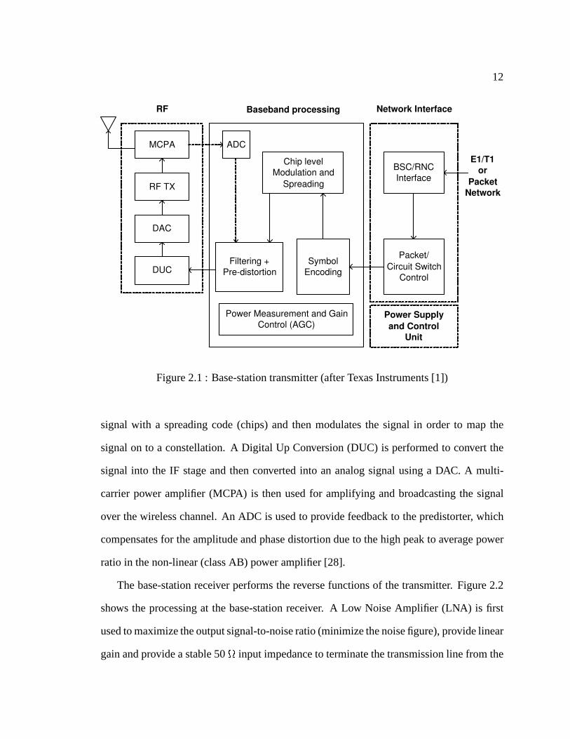
for an introduction). Figure 2.1 shows a detailed diagram ofthe base-station transmitter.
The network interface in the wireless base-station receives the data from a land-line tele-
phone network (for voice) or a packet network (for data) and then sends it to the physical
layer. The physical layer first encodes the data for error correction (symbols), spreads the
12
MCPA
DAC
DUC Filtering +
Pre-distortion
Chip level
Modulation and
Spreading
Symbol
Encoding
Packet/
Circuit Switch
Control
BSC/RNC
Interface
Power Supply
and Control
Unit
Power Measurement and Gain
Control (AGC)
RF Baseband processing Network Interface
E1/T1
or
Packet
Network RF TX
ADC
Figure 2.1 : Base-station transmitter (after Texas Instruments [1])
signal with a spreading code (chips) and then modulates the signal in order to map the
signal on to a constellation. A Digital Up Conversion (DUC) is performed to convert the
signal into the IF stage and then converted into an analog signal using a DAC. A multi-
carrier power amplifier (MCPA) is then used for amplifying and broadcasting the signal
over the wireless channel. An ADC is used to provide feedbackto the predistorter, which
compensates for the amplitude and phase distortion due to the high peak to average power
ratio in the non-linear (class AB) power amplifier [28].
The base-station receiver performs the reverse functions of the transmitter. Figure 2.2
shows the processing at the base-station receiver. A Low Noise Amplifier (LNA) is first
used to maximize the output signal-to-noise ratio (minimize the noise figure), provide linear
gain and provide a stable 50�
input impedance to terminate the transmission line from the

13
LNA
ADC
DDC
Frequency
Offset
Compensation
Channel
estimation
Chip level
Demodulation
Despreading
Symbol
Detection
Symbol
Decoding
Packet/
Circuit Switch
Control
BSC/RNC
Interface
Power and Control
Unit
Power Measurement and
Control
RF Baseband processing Network Interface
E1/T1
or
Packet
Network RF RX
Figure 2.2 : Base-station receiver (after Texas Instruments [1])
antenna to the amplifier. A digital down converter (DDC) is used to bring the signal to
baseband.
The computationally-intensive operations occurring in the physical layer are those of
channel estimation, detection and decoding. Channel estimation refers to the process of
determining the channel parameters such as the amplitude and phase of the received signal.
These parameters are then given to the detector, which detects the transmitted bits. The
detected bits are then forwarded to the decoder which removes the error protection code on
the transmitted signal and then sends the decoded information bits to the network interface
from where it is transferred to a circuit-switched network (for voice) or to a packet network
(for data).
The power consumption of the base-station transmitter is dominated by the MCPA

14
(around 40W/46 dBm [28]) since the data needs to be transmitted over long distances. Also,
the baseband processing of the transmitter is negligible compared to the receiver processing
due to the need for channel estimation, interference cancellation and error correction at the
receiver. The power consumption of the base-station receiver is dominated by the digital
base-band as the RF only uses a low noise amplifier for reception. Although the transmitter
RF power is currently the more dominant power consumption source at the base-station,
the increasing number of users per base-station is increasing the digital processing while
the increasing base-stations per unit area is decreasing the RF transmission power. More
specifically, in proposed indoor LAN systems such as ultrawideband systems, [29] where
the transmit range is around 0�20 meters, the RF power transmission is around 0.55 mW
and the baseband processing is the major source of power consumption. This thesis con-
centrates on the design of programmable architectures for baseband processing in wireless
base-station receivers. It should be noted that flexibilitycan be used in the RF layers as
well to configure to various standards [30], but it’s investigation is outside the scope of this
thesis.
A wide range of signal processing algorithms with increasing complexity and increas-
ing data rates are studied in this thesis to study their impact on programmable architecture
design. Specifically, for evaluation purposes, the algorithms are classified into different
generations (2G, 3G, 4G), which represent increasing complexity in the receiver and in-
creasing data rates. Table 2.1 presents a summary of the algorithms and data rates consid-
ered in this thesis.
2.2 2G CDMA Base-station
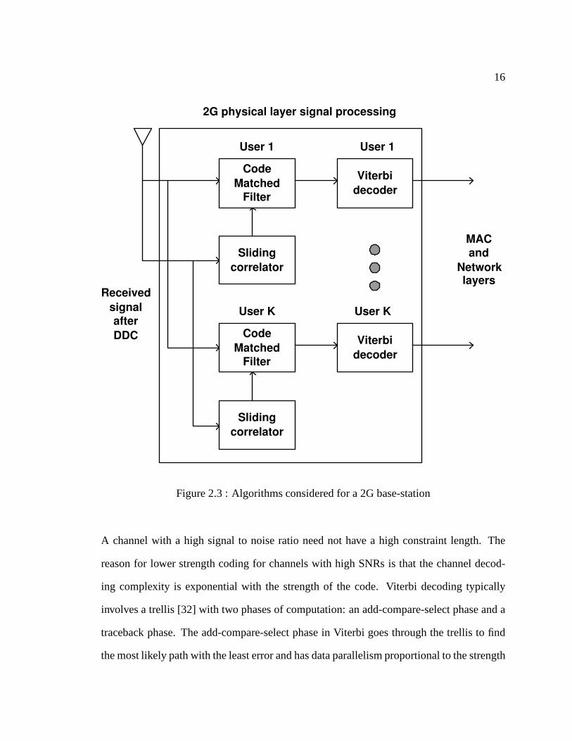
Definition 2.1 For the purposes of this thesis, we will consider a2G base-stationto consist
of simple versions of channel estimation, detection and decoding and which forms a subset

15
Standard Spreading Maximum Target Algorithms
Users Data Rate Estimation Detection Decoding
2G 32 32 16 Kbps Sliding Matched Viterbi
per user Correlator Filter (5,7,9)
3G 32 32 128 Kbps Multiuser Multiuser Viterbi
per user Estimation Detection (5,7,9)
4G 32 32 1 Mbps MIMO Matched LDPC
per user Equalization filter
Table 2.1 : Summary of algorithms, standards and data rates considered in this thesis
of the algorithms used in a subset of a 3G base-station. Specifically, we will consider
a 32-user base-station providing support for 16 Kbps/user (coded data rate) employing a
sliding correlator as a channel estimator, a code matched filter as a detector [31] followed
by Viterbi decoding [32].
Figure 2.3 shows the 2G base-station algorithms consideredin this thesis. A sliding corre-
lator correlates the known bits (pilot) at the receiver withthe transmitted data to calculate
the timing delays and phase-shifts. The operations involved in the sliding correlator used
in our design involves outer product updates. The matched filter detector despreads the
received data and converts the received ’chips’ into ’bits’(’Chips’ are the values of a bi-
nary waveform used for spreading the data ’bits’). The operations involved in matched
filtering at the base-station involves a matrix vector product, with complexity proportional
to the number of users. Both these algorithms are amenable toparallel implementations.
Viterbi decoding [32] is used to remove the error control coding done at the transmitter.
The strength of the error control code is usually dependent on the severity of the channel.
16
Sliding
correlator
Code
Matched
Filter
Viterbi
decoder
MAC
and
Network layers
Received
signal
after
DDC
2G physical layer signal processing
Sliding
correlator
Code
Matched
Filter
Viterbi
decoder
User 1
User K
User 1
User K
Figure 2.3 : Algorithms considered for a 2G base-station
A channel with a high signal to noise ratio need not have a highconstraint length. The
reason for lower strength coding for channels with high SNRsis that the channel decod-
ing complexity is exponential with the strength of the code.Viterbi decoding typically
involves a trellis [32] with two phases of computation: an add-compare-select phase and a
traceback phase. The add-compare-select phase in Viterbi goes through the trellis to find
the most likely path with the least error and has data parallelism proportional to the strength

17
(constraint length) of the code. However, the traceback phase traces the trellis backwards
and recovers the transmitted information bits. This traceback is inherently sequential and
involves dynamic decisions and pointer-based chasing. With large constraint lengths, the
computational complexity of Viterbi decoding increases exponentially and becomes the
critical bottleneck, especially as multiple users need to be decoded simultaneously in real-
time. This is the main reason for Viterbi accelerators in theC55x DSP and co-processors in
the C6416 DSP from Texas Instruments as the DSP cores are unable to handle the needed
computations in real-time.
2.2.1 Received signal model
We assume BPSK modulation and use direct sequence spread spectrum signaling, where
each active mobile unit possesses a unique signature sequence (short repetitive spreading
code) to modulate the data bits (� �). The base-station receives a summation of the signals
of all the active users after they travel through different paths in the channel. The multipath
is caused due to reflections of the transmitted signal that arrive at the receiver along with
the line-of-sight component. These channel paths induce different delays, attenuations and
phase-shifts to the signals and the mobility of the users causes fading in the channel. More-
over, the signals from various users interfere with each other in addition to the Additive
White Gaussian noise (AWGN) present in the channel. The model for the received signal
at the output of the multipath channel [33] can be expressed as
�� � � � � � �� � (2.1)
where�� � � � is the received signal vector after chip-matched filtering [31, 34], � �
� � � is the effective spreading code matrix, containing information about the spreading
codes (of length� ), attenuation and delays from the various paths,� � � �
�
��� ��� �

18�� ����� � � ��� � � � ���� � � ���� are the bits of� users to be detected,�� is AWGN and is
the time index. The size of the data bits of the users�� is �� as we assume that all paths
of all users are coarse synchronized to within one symbol period from the arbitrary timing
reference. Hence, only two symbols of each user will overlapin each observation window.
This model can be easily extended to include more general situations for the delays [35],
without affecting the derivation of the channel estimationalgorithms. The estimate of the
matrix � contains the effective spreading code of all active users and the channel effects
and is used for accurately detecting the received data bits of various users. We will call this
estimate of the effective spreading code matrix,�� , our channel estimate as it contains the
channel information directly in the form needed for detection.
Consider� observations of the received vector� � � �� � � � corresponding to the
known training bit vectors � � � � � . Given the knowledge of the training bits, the
discretized received vectors� �, ��, , � are independent and each of them is Gaussian
distributed. Thus, the likelihood function becomes
p�� � � �� � � � �� � � � � � � � � �� � exp
�
��� � ��� � � � �� ��� � � � ��
After eliminating terms that do not affect the maximization, the log likelihood function
becomes ��� � ��� � � � �� ��� � � � �� (2.2)
The estimate�� , that maximizes the log likelihood, satisfies the followingequation:��� �� � ��� (2.3)
The matrices���
and���
are defined as follows:��� ���� � ��� ��� �
��� � � ��� (2.4)

19
Ignoring the interference from other users for a simple 2G system consideration sup-
porting only voice users (can tolerate more errors), the auto-correlation matrix can be as-
sumed to be an identity matrix, giving a sliding correlator equivalent channel estimate.
�� � ��� (2.5)
For an asynchronous system with BPSK modulation, the channel �� estimate can be ar-
ranged as� � �� � � � � which corresponds to partial correlation information for the
successive bit vectors� ��� � � � � �� �� � �� , which are to be detected. The matched filter
for the asynchronous case is given by
� � � � ���� ���� � ��� �� � (2.6)
� � � ��� �� � �
Based on the algorithms implemented in the 2G base-station,the operation count needed
for attaining 16 Kbps/user data rate and the memory requirements based on a fixed point
analysis is estimated. The breakup of the operation count and the memory requirements
for a 2G base-station are shown in Figures 2.4 and 2.5. A 2G base-station is seen to require
up to 2 GOPs of computation and 120 KB of memory. The operationcount and memory
requirements are used in later chapters to evaluate the choice of DSPs and the amount of
computational power and memory requirements in the DSPs.
2.3 3G CDMA Base-station
Definition 2.2 For the purposes of this thesis, a3G base-stationcontains the elements of a
2G base-station, along with some more sophisticated signalprocessing elements for better
accuracy of channel estimates and for eliminating interference between users. Specifically,

20
1 2 3 4 5 6 7 80
0.2
0.4
0.6
0.8
1
1.2
1.4
1.6
1.8
2
2G base−station load scenarios
Ope
ratio
n co
unt (
in G
OP
s)
Case 1,2: 4 users, K = 7,9
Case 3,4: 8 users, K = 7,9
Case 5,6: 16 users, K = 7,9
Case 7,8: 32 users, K = 7,9
EstimationDetectionDecoding
Figure 2.4 : Operation count break-up for a 2G base-station
1 2 3 4 5 6 7 80
20
40
60
80
100
120
140
2G base−station load scenarios
Mem
ory
requ
irem
ents
(in
KB
)
Case 1,2: 4 users, K = 7,9
Case 3,4: 8 users, K = 7,9
Case 5,6: 16 users, K = 7,9
Case 7,8: 32 users, K = 7,9
EstimationDetectionDecoding
Figure 2.5 : Memory requirements of a 2G base-station
we consider a 32-user base-station with 128 Kbps/user (coded), employing multiuser chan-
nel estimation, multiuser detection and Viterbi decoding [10].
Figure 2.6 shows the algorithms considered for a 3G base-station in this thesis. Mul-
tiuser channel estimation refers to the process of jointly estimating the channel parame-
ters for all the users at the base-station. Since the received signal has interference from
other users, jointly estimating the parameters allows use to obtain the optimal maximum-

21
Multiuser
channel
estimation
Code
Matched
Filter
Viterbi
decoder
MAC
and
Network
layers
Received
signal
after
DDC
3G physical layer signal processing
Parallel
Interference
Cancellation
Stages
Multiuser detection
Code
Matched
Filter
Viterbi
decoder
User 1
User K User K
User 1
Figure 2.6 : Algorithms considered for a 3G base-station
likelihood estimate of the channel parameters for all users. However, a maximum like-
lihood estimate has a significant increase in computationalcomplexity over single-user
estimates [36], but provides a much more reliable channel estimate to the detector.
The maximum likelihood solutions also involve matrix inversions, which present dif-
ficulties in numerical stability with finite precision computations and in exploiting data
parallelism in a simple manner. Hence, we used a conjugate-gradient descent based al-
gorithm that was proposed in [37] that approximates the matrix inversions and replaces
the matrix inversion by matrix multiplications, which are simpler to implement and can
be computed in finite precision without loss in bit error rateperformance. The details of

22
the implemented algorithm are presented in [37]. The computations involve matrix-matrix
multiplications of the order of the number of users and the spreading gain.
2.3.1 Iterative scheme for channel estimation
A direct computation of the maximum likelihood based channel estimate �� involves the
computation of the correlation matrices���
and���
, and then the computation of the
solution to (2.3),� ���� � ��
, at the end of the pilot. A direct inversion at the end of the
pilot is computationally expensive and delays the start of detection beyond the pilot. This
delay limits the information rate. In our iterative algorithm, we approximate the maximum
likelihood solution based on the following ideas:
1. The product� ���� � ��
can be directly approximated using iterative algorithms such as
the gradient descent algorithm [38]. This reduces the computational complexity and
is applicable in our case because���
is positive definite (as long as� � �� ).
2. The iterative algorithm can be modified to update the estimate as the pilot is being
received instead of waiting until the end of the pilot. Therefore, the computation per
bit is reduced by spreading the computation over the entire training duration. During
the �� bit duration, the channel estimate,�� , is updated iteratively in order to get
closer to the maximum likelihood estimate for training length of . Therefore, the
channel estimate is available for use in the detector immediately after the end of the
pilot sequence.
The computations in the iterative scheme during the�� bit duration are given below:� ����� � � ������� � ��� (2.7)� ����� � � ������� � � ��� (2.8)�� ��� � �� ������ � �� ����� � �� �����
�
� ����� � (2.9)

23
The term�� ����� � �� ������
� ����� � in step 3 is the gradient of the likelihood function in (2.2)
at �� ����� for a training length of. The constant� is the step size along the direction of the
gradient. Since the gradient is known exactly, the iterative channel estimate can be made
arbitrarily close to the maximum likelihood estimate by repeating step 3 and using a value
� that is lesser than the reciprocal of the largest eigenvalueof� ����� . In our simulations, we
observe that a single iteration during each bit duration is sufficient in order to converge to
the maximum likelihood estimate by the end of the training sequence. The solution con-
verges monotonically to the maximum likelihood estimate with each iteration and the final
error is negligible for realistic system parameters. A detailed analysis of the determinis-
tic gradient descent algorithm can be found in [38] and a similar iterative algorithm for
channel estimation for long code CDMA systems is analyzed in[39].
An important advantage of this iterative scheme is that it lends itself to a simple fixed
point implementation, which was difficult to achieve using the previous inversion scheme
based on maximum likelihood [33]. The multiplication by theconvergence parameter� can
be implemented as a right-shift, by making it a power of two asthe algorithm converges
for a wide range of� [39].
The proposed iterative channel estimation can also be easily extended to track slowly
time-varying channels. During the tracking phase, bit decisions from the multiuser detector
are used to update the channel estimate. Only a few iterations need to be performed for a
slowly fading channel and the previous estimate serves as aninitialization. The correlation
matrices are maintained over a sliding window of length� as follows,� ����� � � ������� � ��� � ����� � (2.10)� ����� � � ������� � � ��� � �� ���� (2.11)

24
2.3.2 Multiuser detection
Multi-user detection [40] refers to the joint detection of all the users at the base-station.
Since all the wireless users interfere with each other at thebase-station, interference can-
cellation techniques are used to provide reliable detection of the transmitted bits of all
users. The detection rate directly impacts the real-time performance. We choose a parallel
interference cancellation based detection algorithm [41]for implementation which has a
bit-streaming and parallel structure using only adders andmultipliers. The computations
involve matrix-vector multiplications of the order of the number of active users in the base-
station.
The multistage detector [41, 42] performs parallel interference cancellation iteratively
in stages. The desired user’s bits suffers from interference caused by the past or future over-
lapping symbols of various asynchronous users. Detecting ablock of bits simultaneously
(multishot detection) can give performance gains [31]. However, in order to do multishot
detection, the above model should be extended to include multiple bits. Let us consider�bits at a time ( � �� � � � � � �� ). So, we form the multishot received vector� � � � � by
concatenating� vectors��� � � �� � � � � � �� �.
� �
���������
� � � � � �� � � � � �...
. . . . . . � �� � � � �
��������
���������
� �� �...
��
��������� �� (2.12)
Let � � � � � represent the new multishot channel matrix. The initial soft decision
outputs� ��� � � � and hard decision outputs�� ��� � � � of the detector are obtained

25
from a matched filter using the channel estimates as
� ��� � � �� � � � (2.13)�� ��� � ��� �� ��� � � (2.14)
� ��� � � ����
� �� �
��� �� �� �� ����� � (2.15)�� ��� � ��� �� ��� � � (2.16)
where� ��� and �� ��� are the soft and hard decisions respectively, after each stage of the
multistage detector. These computations are iterated for� � �� � � � � � �� where�
is the
maximum number of iterations chosen for desired performance. The structure of� �
� � � is as shown:���������
��� � � ��� � � � �
��� � � ��� � � � ��� � � ��� � � �
.... . . . . .
...� � ��� � � ��� � � � ��� � �
��������
(2.17)
The block tri-diagonal nature of the matrix arises due to theassumption that the asyn-
chronous delays of the various users are coarse synchronized within one symbol dura-
tion [33, 35]. If the channel is static, the matrix is also block-Toeplitz. We exploit the
block tri-diagonal nature of the matrix later, for reducingthe complexity and pipelining
the algorithm effectively. The hard decisions,��, made at the end of the final stage, are
fed back to the estimation block in the decision feedback mode for tracking in the absence
of the pilot signal. Detectors using differencing methods have been proposed [42] to take
advantage of the convergence behavior of the iterations. Ifthere is no sign change of the
detected bit in succeeding stages, the difference is zero and this fact is used to reduce the
computations. However, the advantage is useful only in caseof sequential execution of the
detection loops, as in DSPs. Hence, we do not implement the differencing scheme in our

26
design for a VLSI architecture.
Such a block-based implementation needs a windowing strategy and has to wait until all
the bits needed in the window are received and are available for computation. This results in
taking a window of� bits and using it to detect� �
� bits as the edge bits are not detected
accurately due to windowing effects. Thus, there are 2 additional computations per block
and per iteration that are not used. The detection is done in blocks and the two edge bits are
thrown away and recalculated in the next iteration. However, the stages in the multistage
detector can be efficiently pipelined [43] to avoid edge computations and to work on a bit
streaming basis. This is equivalent to the normal detectionof a block of infinite length,
detected in a simple pipelined fashion. Also, the computations can be reduced to work on
smaller matrix sets. This can be done due to the block tri-diagonal nature of the matrix�� � as seen from (2.17). The computations performed on the intermediate bits reduce to
� � � � ���� �� � � (2.18)
� � � � ���� �� � � ���� �� ��
��� � ���� �� � � ���� �� ��� (2.19)
� ���� � � �����
� �� ���������
� �� �������
�� �� ������� � (2.20)�� ���� � ��� �� � ��� � (2.21)
Equation (2.20) may be thought of as subtracting the interference from the past bits of
users, who have more delay, and the future bits of the users, who have less delay than the
desired user. The left matrix� � � , stands for the partial correlation between the past
bits of the interfering users and the desired user, the rightmatrix�� , stands for the partial
correlation between the future bits of the interfering users and the desired user. The center
matrix� � � , is the correlation of the current bits of interfering usersand the diagonal
elements are made zeros since only the interference from other users, represented by the
non-diagonal elements, needs to be canceled. The lower index, , represents time, while

27
1 2 3 4 5 6 7 80
5
10
15
20
25
3G base−station load scenarios
Ope
ratio
n co
unt (
in G
OP
s)
Case 1,2: 4 users, K = 7,9
Case 3,4: 8 users, K = 7,9
Case 5,6: 16 users, K = 7,9
Case 7,8: 32 users, K = 7,9
Multiuser estimationMultiuser detectionDecoding
Figure 2.7 : Operation count break-up for a 3G base-station
the upper index,�, represents the iterations. The initial estimates are obtained from the
matched filter. The above equation (2.20) is similar to the model chosen for output of the
matched filter for multiuser detection in [44]. The equations (2.20)-(2.21) are equivalent to
the equations (2.15)-(2.16), where the block-based natureof the computations are replaced
by bit-streaming computations.
The breakup of the operation count and the memory requirements for a 3G base-station
are shown in Figure 2.7 and Figure 2.8. An increase in complexity can be observed in the
3G case to 23 GOPs, increasing from 2 GOPs in 2G with an increase in memory require-
ments from 120 KB to 230 KB. However, note that the increase inGOPs is less due to the
increase in the number of operations than due to the increasein the data rates.
2.4 4G CDMA Base-station
Definition 2.3 For a4G system[45], we consider a Multiple Input Multiple Output (MIMO)
system with multiple antennas at the transmitter and receiver. The MIMO receiver employs
chip-level equalization followed by despreading and Low Density Parity Check (LDPC)

28
1 2 3 4 5 6 7 80
50
100
150
200
250
3G base−station load scenarios
Mem
ory
requ
irem
ents
(in
KB
)
Case 1,2: 4 users, K = 7,9
Case 3,4: 8 users, K = 7,9
Case 5,6: 16 users, K = 7,9
Case 7,8: 32 users, K = 7,9
Multiuser estimationMultiuser detectionDecoding
Figure 2.8 : Memory requirements of a 3G base-station
decoding and provides 1 Mbps/user.
Multiple antenna systems have been shown to provide diversity benefits equal to the
product of the number of transmit and receive antennas and a capacity increase to the min-
imum of the number of the transmit and receive antennas [45, 46]. MIMO systems can
provide higher spectral efficiency (bits/sec/Hz) than single antenna systems and can help
support high data rates by simultaneous data transmission on all the transmit antennas in
addition to higher modulation schemes. Both MIMO and multiuser systems share similar
signal processing and complexity tradeoffs [46]. A single user system with multiple anten-
nas appears very similar to a multi-user system. The MIMO base-station model is shown
in Figure 2.9.
2.4.1 System Model
For the purposes of this thesis, we will consider a model withT transmit antennas per
user, M receive antennas at the base-station, K users, spreading code of length G, QPSK
modulation, with data in real-part, and training on the imaginary part of the QPSK symbol

29
M-antenna
Base-station
Mobile user 1
Mobile user K
MIMO Channel KT x M
Figure 2.9 : MIMO system model
on each antenna, with a 32 Mbps real-time target (�� over 3G). The current model is based
on extending a similar MIMO model for the downlink [47] to theuplink. Figure 2.10 shows
the algorithms considered for a 4G base-station in this thesis.
The use of a complex scrambling sequence in considered for 4Gsystems in this thesis
and requires the need for chip-level equalization as opposed to symbol level channel esti-
mation and detection in the 3G workload considered earlier�. The use of the scrambling
sequence also whitens the noise, reducing the performance benefits of multiuser detection
in the 4G system considered. Hence, multiuser detection schemes have not been considered
as part of the 4G system model. The base-station performs chip-level equalization on the
received signal and equalizes the channel between each transmit antenna of each user and
the base-station. A conjugate-gradient descent [38] scheme as proposed in [47] is used to
�An actual 3G system [14] uses scrambling sequences (long codes), but is not considered in the 3G
system workload of this thesis due to the use of multiuser estimation and detection algorithms that need short
spreading sequences

30
Received
signal
after DDC
4G physical layer signal processing
Channel
Estimation
LDPC
decoder
MAC
and
Network
layers Channel
estimation
User 1, Antenna 1
User 1, Antenna T
M antennas
User 1
Code
Matched
Filter
Chip level
Equalization
Code
Matched
Filter
Chip level
Equalization
Channel
Estimation
LDPC
decoder
Channel
estimation
User K, Antenna 1
User K, Antenna T
User K
Code
Matched
Filter
Chip level
Equalization
Code
Matched
Filter
Chip level
Equalization
Figure 2.10 : Algorithms considered for a 4G base-station

31
perform the chip level equalization and update the chip matched filter coefficients used in
the equalizer. The symbol is then code match filtered and thensent to the decoder.
2.4.2 Chip level MIMO equalization
1. Calculate the covariance matrix
��r� ��
���� � � ���� �� (2.22)
where��� is the vector of
� �� � �� chips combined from all receive�
antennas.
This is an outer product update, giving a output complex matrix� �
of size� �� �
�� � � �� � ��.Parameters chosen are� � � �� � �� � ��. This is similar to the outer-product
auto-correlation update in channel estimation for 3G, except that it is done at the chip
level, which implies higher complexity.
2. Estimate the channel response (channel estimation)
Estimation of the channel impulse response between transmit antenna� and receive
antenna� is determined as:
��� �� ��� ��
�� ��
���� � � �� � ��� �� �� ��� � � � �� � � � � � �� �� � � �� ��(2.23)
This is similar to the outer-product cross-correlation update in channel estimation for
3G. The complete matrix is of size� �� � �� � � � . It is better to put� as the
column dimension as all users can be done in parallel and makes stream processor
implementation simpler.
3. Conjugate Gradient Equalization
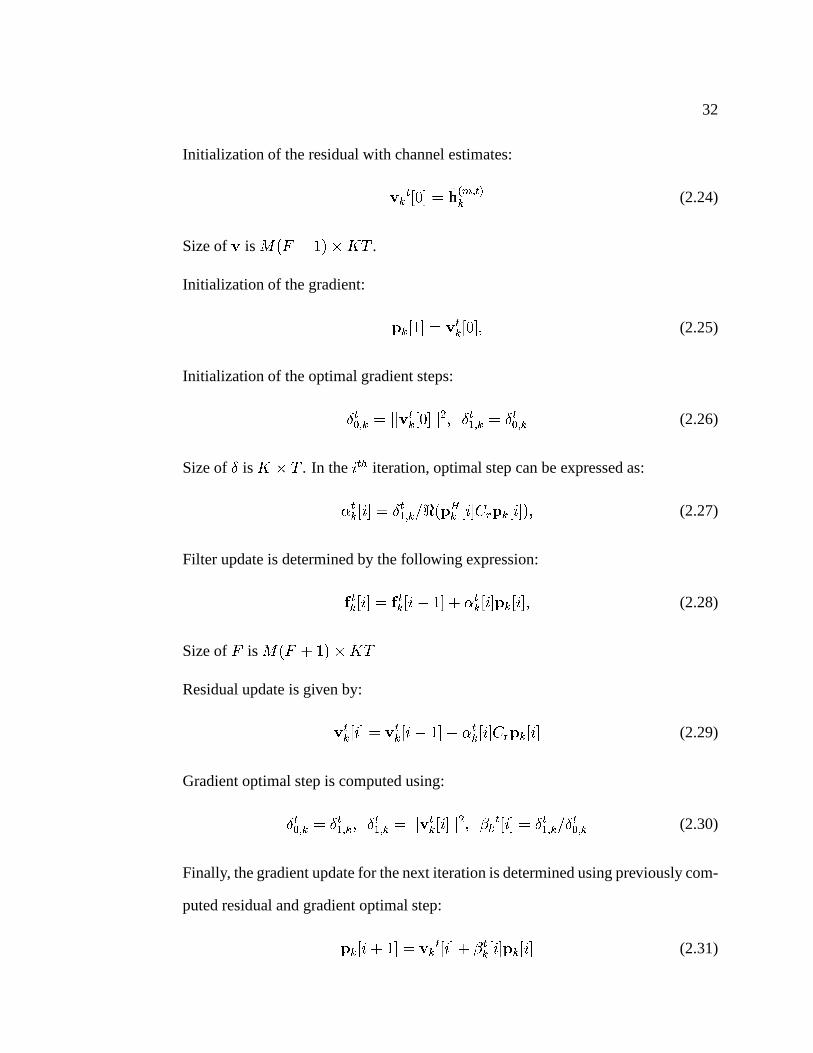
32
Initialization of the residual with channel estimates:
� � � ��� � �� �� ����(2.24)
Size of� is� �� � �� � � � .
Initialization of the gradient:
� � ��� � � �� ��� � (2.25)
Initialization of the optimal gradient steps:
� �� �� � ��� �� ��� ��� � � ���� � � �� �� (2.26)
Size of�
is � � � . In the�� iteration, optimal step can be expressed as:
� �� �� � � ���� �� ���� ��� �� � ��� � (2.27)
Filter update is determined by the following expression:
� �� �� � � �� � � �� � � �� ��� � �� � (2.28)
Size of� is� �� � �� � � �
Residual update is given by:
� �� �� � � �� � � ��� � �� ��� �� � �� (2.29)
Gradient optimal step is computed using:
� �� �� � � ���� � � ���� � ��� �� �� ��� � �� � �� � � ���� �� �� �� (2.30)
Finally, the gradient update for the next iteration is determined using previously com-
puted residual and gradient optimal step:
� � � � �� � � � � �� � � �� ��� � �� (2.31)

33
4. Filtering after finding filter taps
�� �� ��� � � � � � ��� � ��� � � �� � � � � � � � � � (2.32)
�� is the chip estimate, which is of size� � as independent data on each transmit
antenna and each user.� � �� is the number of symbols. The block is of size�� � � � .
5. Despreading and Descrambling
���� ��� � sgn���� � ��� � �� � � � � � � � � ��� �� �� ��� � �� � � � � � � � � �� (2.33)
where� is the symbol number, and�� is the spreading sequence for user.
2.4.3 LDPC decoding
Low Density Parity Check codes are experiencing a renewed interest after they have been
shown to outperform all existing decoders such as Turbo decoders and Viterbi decoders
while requiring lower complexity [48]. It has been shown that LPDC codes, in the limit of
infinite block lengths, can achieve reliable communicationwithin 0.0045 dB of the Shan-
non limit. LDPC codes are a class of linear block codes [32] corresponding to a parity
check matrix . The parity check matrix ���� �� for LDPC codes is a sparse matrix�,consisting of only� ��� and���. Given� information bits, the set of LDPC codewords�
in the code space of length , spans the null space of the parity check matrix in which:� � � �.
A sparse matrix is defined as a matrix having sufficient zeros such that the sparsity can be used to provide
savings in memory and/or computations

34
For a �� � �� � � regular LDPC code each column of the parity check matrix has� ���� and each row has� � ���. If degrees per row or column are not constant, then the
code isirregular. Some of the irregular codes have shown better performance than regular
ones. But irregularity results in more complex hardware andinefficiency in terms of re-
usability of functional units. Code rate�
is equal to� � which means that� � � �redundant bits have been added to the message so as correct the errors.
LDPC codes can be represented effectively by a bi-partite Tanner graph. A bi-partite
graph is a graph (nodes or vertices are connected by undirected edges) whose nodes may be
separated into two classes, and where edges may only be connecting two nodes not residing
in the same class. The two classes of nodes in a Tanner graph are Bit Nodes and Check
Nodes. The Tanner graph of a code is drawn according to the following rule: “Check node�� � � � �� �� � � is connected to bit node� � � � �� �� whenever element�� � in (parity check matrix) is a��.” The LDPC decoding is shown in Figure 2.11.
LDPC decoding is based on belief propagation that uses iterative decoding. While two
types of iterative decoders have been proposed; message passing and bit-flipping [48], in
this thesis, we focus on the message passing algorithm for decoding (also, called sum-
product decoding). To reduce hardware complexity in the sum-product algorithm, we use a
modified min-sum algorithm [49]. The modified Min-Sum algorithm iterates over rows and
columns of the parity-check matrix, , and operates on non-zero entries. In a Tanner graph
related to parity check matrix, edges can be seen as information flow pathways and nodes as
processing units. For the parity check matrix of ���� �� � � � �� � � � � � �� � � ,
assume:
� � �: Received bit.
� �� � � � �� � � ��: The set of column locations of the��� in the� �� row of parity
check matrix .

35
H =
0 1 1 0 1 0 1 0
1 0 1 0 0 1 0 1
0 0 0 1 1 0 0 1
1 1 0 1 0 1 1 0
Q-P
P Q-P Check nodes
P Bit nodes
Wc = degree of column (bit) nodes
Wr = degree of row (check) nodes
Wc P = Wr (Q-P)
Iterate
Check
nodes
Bit
nodes
Detected
bits
Decoded
Symbols
Figure 2.11 : LDPC decoding
� �� �� � � � �� �� � �� �� �: The set of column locations of the��� in the� �� row
of parity check matrix , excluding location.� � � � �� � �� � � ��: The set of row locations of the��� in the �� column of parity
check matrix .
� � ��� � �� � �� � � � �� � �� � �: The set of row locations of the��� in the �� column
of parity check matrix , excluding location� .
� �� �� �� �� �: The message to be passed from Check node��
/(Bit node�� )to Bit node
� �/(Check node��
).
The modified Min-Sum decoding algorithm consists of the following steps:

36
Step 0: Initialization: Read the values from channel in each Bit node � � and send the
messages� �� to corresponding Check nodes��
.
� �� � �� � � � (2.34)
Step 1: Iteration : Compute the messages at Check nodes and pass a unique messages�� �
to each Bit node.
�� � � �� ����� ��� ��� � �������� �� � ��� � (2.35)
where,
� �� � sign���� � � � �� � � ��
Step 2: Compute messages at Bit nodes and pass to Check nodes.
��� � ��� � � ���� �� �� � � � � � (2.37)
in which � is the scaling factor.
Step 3: Update the initial values that were read from channel.
� � �� � � ��� �� � (2.38)
Step 4: Threshold the values calculated in each Bit node to find a codeword. For every
row index:
��� � ����
� � � � �� ����
(2.39)
Compare the codeword with set of valid codewords. If�� � � � or if maximum
number of iteration is reached then stop, else go to step 1.

37
1 2 30
20
40
60
80
100
120
140
160
180
Antenna configurations: 1x2, 2x4, 4x8
Arit
hmet
ic o
pera
tion
coun
t (G
OP
s)
Chip level equalization, matched filtering(3,6) LDPC decoding of 2048 blocks
Figure 2.12 : Operation count break-up for a 4G base-station
2.4.4 Memory and operation count requirements
The breakup of the operation count and the memory requirements for a 4G base-station are
shown in Figure 2.12 and Figure 2.13. An increase in complexity can be observed in the 4G
case to 190 GOPs for the 2x4 antenna configuration, increasing from 23 GOPs in 3G. The
memory requirements are not much affected by the algorithms. Thus, we can see that, as
algorithms change and data rates increase from 2G to 3G to 4G,the amount of computations
per second increase almost by an order-of-magnitude compared to the marginal increase in
memory requirements. However, this implies that memory bandwidth requirements need
to be increased in order to support more computations/second.
2.5 Summary
This chapter presents the compute requirements of some of the computationally complex
wireless algorithms considered for cellular base-stations in this thesis. Signal processing
algorithms used in wireless cellular base-stations show significant amounts of data par-

38
1 2 30
50
100
150
200
250
300
350
Antenna configurations: 1x2, 2x4, 4x8
Dat
a m
emor
y re
quire
men
ts (
KB
)
Chip level equalization,matched filtering(3,6) LDPC decoding of 2048 blocks
Figure 2.13 : Memory requirements of a 4G base-station
allelism. As wireless systems have evolved over time, therehas been an increase in the
compute performance needed in wireless systems due to the simultaneous increase in data
rates and the increase in the complexity of signal processing algorithms for better perfor-
mance. This increase in compute requirements with significant data parallelism availability
motivates the need for high performance data-parallel DSP design. The next chapter talks
about existing DSP architectures for implementing such algorithms and chapter 5 presents
efficient mapping of these algorithms on stream processors.

39
Chapter 3
High performance DSP architectures
This chapter introduces the various types of high-performance processors that are used for
designing wireless communication systems.
3.1 Traditional solutions for real-time processing
DSP architectures designs have traditionally focused on providing and meeting real-time
constraints, for example, in cellular base-station [5]. The other factors have been cost, flex-
ibility and time-to-market. Advanced signal processing algorithms, such as those in base-
station receivers, present difficulties to the designer dueto the implementation of complex
algorithms, higher data rates and desire for more channels (mobile users) per hardware
module. A key constraint from the manufacturing point of view is attaining a high channel
density. This implies that a large number of mobile users need to be processed by a single
hardware module (RF interface + DSP + co-processors) [5].
Traditionally, real-time architecture designs employ a mix of DSPs, co-processors, FP-
GAs, ASICs and application-specific standard parts (ASSPs)for meeting real-time require-
ments in high performance applications such as wireless base-stations [2–5]. Figure 3.1,
for example, shows a traditional base-station architecture design. The chip rate processing
is handled by the ASSP, ASIC or FPGA while the DSPs handle the symbol rate processing
and use co-processors for decoding. The DSP can also implement parts of the MAC layers
and control protocols or can be assisted by a RISC processor.

40
‘Chip rate’
processing
‘Symbol rate’
processing
Decoding
Control and
protocol
RF
(Analog)
ASIC(s)
and/or
ASSP(s)
and/or
FPGA(s)
DSP(s)
Co-processor(s)
and/or
ASIC(s)
DSP or
RISC
processor
Figure 3.1 : Traditional base-station architecture designs [2–5]
The heterogeneous nature of the architecture workloads (mix of ASICs,DSPs,FPGAs,
co-processors) in traditional designs make partitioning of the workloads and programming
them in this heterogeneous environment an important research challenge [50, 51]. How-
ever, dynamic variations in the system workload such as variations in the number of users
in wireless base-stations, will require a dynamic re-partitioning of the algorithms which
may not be possible to implement in traditional FPGAs and ASICs in real-time. The het-
erogeneous nature of the workload also impacts channel density as single-chip integration
of the entire system will present difficulties in programming and adapting the various het-
erogeneous modules on the same chip.
This thesis presents the hypothesis that DSP architecturescan be designed to meet real-
time requirements in wireless systems without the use of application-specific hardware.
Hence, this thesis restricts the DSP design to homogeneous,programmable architectures
that meet the following criteria:
1. The programmable DSP architectures are fixed-point processors. This is because
signal processing algorithms can be typically implementedin finite precision, often

41
with less than or equal to 16-bit precisions [10]. This allows for power efficiency in
the design.
2. The DSPS can support 100 or more arithmetic units to meet real-time constraints.
3. The DSPs architectures do not have any application-specific optimization that is ren-
dered useless by the lack of use of that application. For example, this thesis does not
consider providing an instruction for Viterbi ACS [52] or Viterbi co-processors as
in the TI C6416 DSP [13, 53]. This is because such instructions or hardware cannot
be re-used by other applications and limits the programmability of the system. The
design choice to provide a high degree of programmability automatically precludes
solutions such as combinations of DSPs with ASICs, FPGAs with static reconfigu-
ration, application-specific co-processors for DSPs and application-specific standard
processors (ASSPs) in this thesis.
3.2 Limitations of single processor DSP architectures
Traditional single processor DSP architectures such as theC64x DSP by Texas Instru-
ments [13] employ VLIW architectures and exploit instruction level parallelism (ILP) and
subword parallelism. Such single processors DSPs can only have limited arithmetic units
(less than 10) and cannot directly extend their architectures to 100’s of arithmetic units.
This is because, as the the number of arithmetic units increases in an architecture, the size
of the register files and the port interconnections start dominating the architecture [11, 12].
This growth is shown as a cartoon in Figure 3.2. The cartoon isused to show that, for�
arithmetic units, the area of the register files grows as� � [54]. While the use of distributed
register files may alleviate the register file explosion at the cost of increased penalty in reg-
ister allocation [11], there is an associated cost in exploiting ILP due to limited size of reg-

42
32
Register
File
RF 16
32 ALUs
Register
File
1 ALU
RF 4 ALUs
16 ALUs
1 cm
1 cm
Figure 3.2 : Register file explosion in traditional DSPs withcentralized register files. Cour-tesy: Scott Rixner
ister files, dependencies in the computations and the register and functional unit allocation
and utilization efficiency of the compiler. It has been shownthat even with sophisticated
techniques, it is very difficult to exploit ILP beyond 5 [55].Hence, multi-processor DSP
solutions are required to support 100’s of arithmetic units.
3.3 Programmable multiprocessor DSP architectures
This thesis considers multiprocessors that are completelyprogrammable and have the po-
tential to support greater than 100 arithmetic units. Multiprocessor architectures can be
classified into Single Instruction Multiple Data (SIMD) andMultiple Instruction Multiple
Data (MIMD) architectures, based on the Flynn taxonomy [56]. For the convenience of
this thesis, we classify them further as shown in Figure 3.3.Some of the examples shown
in Figure 3.3 may fit in other categories as well. The following subsections traverse the
figure from left to right to demonstrate the benefits of exploiting explicit data parallelism
for DSPs. The figure shows that the combination of exploitinginstruction level parallelism

43
(ILP) and Data Parallelism (DP) leads to the design of data-parallel DSPs. Data-parallel
DSPs exploit data parallelism, instruction level parallelism and subword parallelism. Al-
ternate levels of parallelism such as thread level parallelism exist and can be considered
after this architecture space has been fully studied and explored.
3.3.1 Multi-chip MIMD processors
The first MIMD processors have been implemented as loosely coupled architectures as in
the Carnegie Mellon Star machine (Cm�) [58]. Each processor in a loosely coupled system
has a set of I/O devices and a large local memory. Processors communicate by exchanging
messages using some form of message-transfer system [58]. Loosely coupled systems are
efficient when interaction between tasks are minimal. Loosely coupled DSP architectures
have been used in the TI C4x processors [59, 60], where the communication between pro-
cessors is done using communication ports. The tradeoffs ofthis processor design have
been the increase in programming complexity and the need forhigh I/O bandwidth and
inter-processor support. Such MIMD solutions are also difficult to scale with processors.
While the C4x processor is no longer used due to the design of higher performance VLIW
DSPs such as the C6x [13], many 3rd party DSP vendors such as Sundance [61] use com-
munication libraries built around the C4x communication ports and use FPGAs to provide
the interconnection network. The disadvantages of the multi-chip MIMD model and archi-
tectures are the following:
1. Load-balancing algorithms for such MIMD architectures is not straight-forward [62]
similar to heterogeneous systems studied earlier in this chapter. This makes it diffi-
cult to partition algorithms on this architecture model especially when the workload
changes dynamically.

44
2. The loosely coupled model is not scalable with the number of processors due to
interconnection and I/O bandwidth issues [58].
3. I/O impacts the real-time performance and power consumption of the architecture.
4. Design of a compiler for a MIMD model on a loosely coupled architecture is difficult
and the burden is left to the programmer to decide on the algorithm partitioning on
the multiprocessor.
3.3.2 Single-chip MIMD processors
Single-chip MIMD processors can be classified into 3 categories: single-threaded chip
multiprocessors (CMPs), multi-threaded multiprocessors(MTs) and clustered VLIW ar-
chitectures as shown in Figure 3.3. A CMP integrates two or more complete processors
on a single chip [63]. Therefore, every unit of a processor isduplicated and used inde-
pendently of its copies. In contrast, a multi-threaded processor interleaves the execution of
instructions of various threads of control in the same pipeline. Therefore, multiple program
counters are available in the fetch unit and multiple contexts are stored in multiple registers
on the chip. The latencies that arise during computation of asingle instruction stream are
filled by computations of another thread, thereby providingbetter functional unit utilization
in the architecture. The TI C8x Multimedia Video Processor (MVP) [64] is the first CMP
for DSPs developed at TI. Other CMP systems have been proposed such as Cradle’s 3SoC,
Hydra and the IBM Power4 [63, 65]. Multi-threading increases instruction level parallelism
in the arithmetic units by providing access to more than a single independent instruction
stream. Since, the programmer has a detailed knowledge of interdependencies and sub-
tasks in many signal processing applications, control instructions for independent threads
can be easily inserted and this has been shown to be provide benefits in image processing

45
applications [66].
Clustered VLIW architectures are another example of VLIW architectures that solve
the register explosion problem by employing clusters of functional units and register files.
Clustering improves cycle time in two ways: by reducing the distance the signals have to
travel within a cycle and by reducing the load on the bus [12].Clustering is beneficial for
applications which have limited inter-cluster communication. However, compiling for clus-
tered VLIW architectures can be difficult in order to schedule across various clusters and
minimize inter-cluster operations and their latency. The compilation problem gets harder
with increasing the number of clusters [12, 67, 68]. Hence, clustered VLIW architectures
typically use a very small number of clusters. For example, the TI C6x series of high
performance DSPs use 2 clusters [69] while the multiflow TRACE architecture used 2-4
clusters [70].
Although single chip MIMD architectures eliminate the I/O bottleneck between multi-
ple processors, the load balancing and architecture scaling issues still remain. Currently,
single chip MIMD architectures do not scale to providing 100’s of arithmetic units in the
processor and allowing tools and compilers to load balance the architecture efficiently. The
availability of data parallelism in signal processing applications is not utilized efficiently in
MIMD architectures.
3.3.3 SIMD array processors
SIMD processing refers to processing of identical processors in the architecture that execute
the same instruction but work on different sets of data in parallel. An SIMD array processor
is referred to processor designs targeted towards implementation of arrays or matrices.
There are various types of interconnection methodologies used for array processors such
as linear array (vector), ring, star, tree, mesh, systolic arrays and hypercubes. For example,

46
Illiac-IV implemented a mesh network array of 64 processorsand the Burroughs Scientific
Processor (BSP) implemented a linear vector processor but with a prime number of memory
banks to reduce memory-bank conflicts [58]. ClearSpeed [71]is another example of a
vector processor that only has nearest neighbor connections. Although vector processors
have been the most popular version of array processors, meshbased processors are still
being used in scientific computing.
3.3.4 SIMD vector processors
The high levels of data parallelism demonstrated in chapter2 allow vector processors to
approach the performance and power efficiency of custom designs, while simultaneously
providing the flexibility of a programmable processor [72].Vector machines were the
first attempt at building super-computers, starting from the Cray-1 machine in 1972 [58].
Vector processors such as Cray-1 were traditionally designed to exploit data parallelism
but did not exploit instruction level or sub-word parallelism. These processors executed
vector instructions such as vector adds and multiplications out of a vector register file. The
number of memory banks is equal to the number of processors such that all processors can
access memory in parallel. Newer vector processors such as vector IRAM and CODE [72]
exploit ILP, subword and data parallelism and have been proposed for media processing
applications.
3.3.5 Data-parallel DSPs
The thesis defines data-parallel DSPs as architectures thatexploit ILP, SubP and DP as
explained in Figure 3.3. Examples of such processors are IBM’s eLiteDSP [57], Motorola’s
RVSP [73] and the Imagine stream processor from Stanford [74].
Stream processors are state-of-the-art programmable architectures aimed at media pro-

47
cessing applications. Stream processors enhance data-parallel DSPs by providing a band-
width hierarchy for data flow in signal processing applications that enable support for hun-
dreds of arithmetic units in the data-parallel DSP.
Definition 3.1 Streamsrefer to the data which is produced or acquired as a stream of
elements, each of which is relevant for a short period of time, and which goes through
the same computations. The characteristics of data streamsare that elements have a high
degree of spatial locality, but limited temporal locality [73, 74].
In addition to having spatial locality, data access patterns in stream processor applica-
tions are such that entire input and output sets are known prior to the computations. These
characteristics allow prefetching of data, hiding memory latencies.
Stream processors exploit data parallelism similar to vector processors but with a few
differences as shown in [22]. The key differences are in the use of a bandwidth hierarchy
and in instruction sequencing, allowing it to reduce bandwidth demands on memory and al-
lowing support for more ALUs than a vector processor for a given memory bandwidth [22].
Stream processors can also be thought of as clustered VLIW processors with the exception
that each cluster works with the same instruction. This allows stream processors to exploit
data parallelism instead of ILP and also allows the ability to support a larger number of
clusters in the architecture. The thesis specifically focuses on stream processors as an ex-
ample of data-parallel DSPs and uses stream processors to evaluate the contributions of this
thesis. Stream processors are explained in more detail in the next chapter.
3.3.6 Pipelining multiple processors
An alternate method to attain high data rates is to provide multiple processors that are
pipelined. Such processors would be able to take advantage of the streaming flow of data

48
through the system. The disadvantages of such a design are that the architecture would
need to be carefully designed to match the system throughputand is not flexible enough to
adapt to changes in system workload. Also, such a pipelined system would be difficult to
program and suffer from I/O bottlenecks unless implementedas a SoC. However, this is the
only way to provide desired system performance if the amountof parallelism exploitation
does not meet the system requirements.
3.4 Reconfigurable architectures
Definition 3.2 Reconfigurable� architectures are defined in this thesis as programmable
architectures that change the hardware and/or the interconnections dynamically so as to
provide flexibility with simultaneous benefits in executiontime due to the reconfiguration
as opposed to turning off units to conserve power.
Reconfigurable architectures [4, 75–83] are becoming increasingly popular choices for
wireless systems. Such architectures are more favorable inbase-stations in an initial evalu-
ation phase as they don’t have stringent constraints on power, area, form-factor and weight
as mobile handsets [83].
There have been various approaches to provide and use this reconfigurability in pro-
grammable architectures [4]. The first approach is the ’FPGA+’ approach, which adds a
number of high-level configurable functional blocks to a general purpose device to opti-
mize it for a specific purpose such as wireless [75, 76]. The second approach is to develop
a reconfigurable system around a programmable ASSP. The third approach is based on a
parallel array of processors on a single die, connected by a reconfigurable fabric.
�General definition: A reconfigurable processor is a microprocessor with erasable hardware that can
rewire itself dynamically.

49
3.5 Issues in choosing a multiprocessor architecture for evaluation
The choice of a multiprocessor architecture for a wireless application is not a simple one.
While this thesis primarily targets performance and power,secondary metrics such as cost,
precision, data width, memory, tools and multiprocessor scalability [18] play a major role
in design choices for multiprocessors. Stream processors enhance data-parallel DSPs by
providing a bandwidth hierarchy to support 100’s of arithmetic units. They also have been
implemented, designed and fabricated to verify the system design. Open-source tools are
also available for designing and evaluating stream processors. Stream processors are used
as the reference data-parallel DSP architecture in this thesis to evaluate the contributions of
this thesis.
The architectures and tools that have been developed in the industry are not open-
source, providing little scope for architecture modifications and/or investigating problems
or modifications with tools and compilers. This restricts our choice to academic research
tools, which are open-source, but do not have the complete tool support and/or have tools
still under the evaluation/development phase. Finally, the architecture and tools should
be flexible enough in order to support modifications and also be suitable for application
workloads.
A stream processor simulator based on the Imagine stream processor is available for
public distribution from Stanford. The Imagine simulator could be programmed in a high-
level language and allows the programmer to modify the machine description features such
as number and type of functional units and their latency. Thecycle-accurate simulator
and re-targetable compiler also gives insights into the functional unit utilization, memory
stalls along with the execution time performance for the algorithms. A power consumption
and VLSI scaling model is also available to give a complete picture of area, power and
performance of the final resulting architecture.

50
3.6 Summary
The need for real-time processing in high performance applications make multiprocessor
DSPs necessary to support 100’s of arithmetic units. There are a variety of combinations
for multiprocessor DSPs in the (instruction level parallelism, subword parallelism, data
parallelism, coarse-grained pipelining and multi-threading) space. The greater the types
of parallelism and pipelining exploited in the DSP, the greater is the complexity of the as-
sociated software and compiler tools in order to support thearchitecture. Current single
processor DSPs such as the TI C64x explore the (instruction level parallelism, subword
parallelism) space. This thesis explores the (instructionlevel parallelism, subword paral-
lelism, data parallelism) space using stream processors with increased complexity in the
software and compiler tools for investigating this thesis for performance benefits due to
the abundant data parallelism observed in the algorithms ofchapter 2. The next chapter
presents the architecture framework of stream processors and discusses the complexity of
the tools and the programming language.

51
Multi-chip
Examples:
TI TMS320C40 DSP
Sundance
Cm*
Multiprocessors
SIMD
(Single Instruction
Multiple Data)
MIMD
(Multiple Instructions
Multiple Data)
Single chip
Chip
multiprocessor
(CMP)
Examples:
TI TMS320C8x DSP
Cradle 3SOC TM
Hydra
IBM Power4
Clustered VLIW
Examples:
TI TMS320C6x DSP
Multiflow TRACE
Alpha 21264
Vector
Examples:
CODE
Vector IRAM Cray 1
Array
Examples:
ClearSpeed TM
MasPar
Illiac-IV
BSP
Data-parallel DSP
Examples:
IBM’s eLiteDSP
Stream Processors:
Stanford Imagine
Motorola RSVP TM
Multi-threading
(MT)
Examples:
Sandbridge SandBlaster TM DSP
Cray MTA
M-machine
Sun MAJC
PowerPC RS64IV
Alpha 21464
Reconfigurable
processors
Examples:
RAW
Chameleon
picoChip
Types of Parallelism
Instruction Level
Parallelism
(ILP)
Subword
Parallelism
(SubP)
Data
Parallelism
(DP)
Thread Level
Parallelism
(TLP)
Data-parallel DSP
Figure 3.3 : Multiprocessor classification
52
Chapter 4
Stream processors
4.1 Introduction
Special-purpose processors for wireless communications perform well because of the abun-
dant parallelism and regular communication patterns within physical layer processing.
These processors efficiently exploit these characteristics to keep thousands of arithmetic
units busy without requiring many expensive global communication and storage resources.
The bulk of the parallelism in wireless physical layer processing can be exploited as data
parallelism, as identical operations are performed repeatedly on incoming data elements.
A stream processor can also efficiently exploit data parallelism, as it processes indi-
vidual elements fromstreamsof data in parallel. Figure 4.1 shows the various parallelism
levels exploited by a stream processor. Traditional DSPs exploit instruction level paral-
lelism (ILP) [55] and subword parallelism [84, 85]. Stream processors, being data-parallel
DSPs, exploit data parallelism (DP) similar to Single Instruction Multiple Data (SIMD)
vector processors, in addition to ILP and subword parallelism, enabling high performance
programmable architectures with hundreds of Arithmetic and Logic Units (ALUs).
Definition 4.1 The general definition ofdata parallelismis the number of operations in
the data that can be executed in parallel. Thus, subword parallelism is also a form of data
parallelism. Moreover, in many machines, loops that have data parallelism can be unrolled
to show up as instruction level parallelism. Hence, in this thesis,data parallelismis defined
as the parallelism available in the data after exploiting subword parallelism (packing) and

53
Internal
Memory
+ + +
x
x
x
+ + +
x
x
x
+ + +
x
x
x
+ + +
x
x
x
ILP
SubP ...
DP
(a) Traditional
embedded
processor
(DSP) (b) Data-parallel embedded
stream processor
ILP
SubP
Internal Memory (banked to the number of clusters)
Figure 4.1 : Parallelism levels in DSPs and stream processors
instruction level parallelism (loop unrolling).
Streams are stored in a stream register file, which can efficiently transfer data to and
from a set of local register files between major computations. Local register files (LRFs),
co-located with the arithmetic units inside the clusters, directly feed those units with their
operands. Truly global data, data that is persistent throughout the application, is stored
off-chip only when necessary. These three explicit levels of storage form an efficient com-
munication structure to keep hundreds of arithmetic units efficiently fed with data. The
Imagine stream processor developed at Stanford is the first implementation of such a stream
processor [22].
Figure 4.2 shows the architecture of a stream processor, with�
arithmetic clusters.
Operations in a stream processor all consume and/or producestreams which are stored

54
C l u
s t e
r C
C l u
s t e
r 0
C l u
s t e
r 1
External Memory (DRAM)
Stream Register File
(SRF) SRF C
Inter-cluster
communication
network
SRF 1 SRF 0
SB SB SB SB
SB SB SB SB
Stream Buffers
(SB)
Clusters
of
Arithmetic Units
M i c
r o - C
o n
t r o l l e
r
Figure 4.2 : A Traditional Stream Processor
in the centrally located stream register file (SRF). The two major stream instructions are
memory transfers and kernel operations. A stream memory transfer either loads an entire
stream into the SRF from external memory or stores an entire stream from to the SRF to
external memory. Multiple stream memory transfers can occur simultaneously, as hardware
resources allow. A kernel operation performs a computationon a set of input streams to
produce a set of output streams. Kernel operations are performed within a data parallel
array of arithmetic clusters. Each cluster performs the same sequence of operations on

55
independent stream elements. The stream buffers (SBs) allow the single port into the SRF
array (limited for area/power/delay reasons) to be time-multiplexed among all the interfaces
to the SRF, making it appear that there are many logical portsinto the array. The stream
buffers (SBs) also act as prefetch buffers and prefetch the data for kernel operations. Both
the SRF and stream buffers are banked to match the number of clusters. Hence, kernels
that need to access data in other SRF banks need to use the inter-cluster communication
network for communicating data between the clusters.
Figure 4.3 shows the internal details of a stream processor cluster. The arithmetic clus-
ters get data from the stream buffers connected to the SRF. The local register files (LRF)
enable support for 10’s of ALUs within each cluster, overcoming the register file area and
interconnection network explosion with increasing ALUs inthe traditional centralized reg-
ister file architectures [54]. Kernels executing in the arithmetic clusters, sometimes need
to index into small arrays or lookup tables. The scratchpad unit in the clusters provide
this functionality. The intra-cluster communication network allows communication of data
within the cluster ALUs and the scratchpad while the inter-cluster communication network
allows communication of data across clusters. The inter-cluster communication unit is used
for applications that are not perfectly data parallel and need to communicate variables or
data across clusters. The inter-cluster communication is performed by the communication
unit within each cluster.
4.2 Programming model of the Imagine stream processor
Stream applications are programmed at two levels: kernel and stream. The kernel code
represents the computation occurring in the applications while the stream code represents
the data communication between the kernels. Figure 4.4 shows the stream processor pro-
gramming model. The kernel code takes the input stream data,performs the computations

56
+
/
+
/
+
+
+
x
x
x
+
+
+
x
x
x
+
/
+
/
+
+
+
+
+
+
x
x
x
x
x
x
+
+
+
+
+
+
x
x
x
x
x
x
Distributed Register Files
(supports more ALUs)
Inter-cluster
communication network
Intra-cluster
communication network
SRF
To/From SRF
Scratchpad
(indexed accesses) Comm. unit
Figure 4.3 : Internal details of a stream processor cluster,adapted from Scott Rixner [6]
and produces output streams, while the stream code direct the dataflow within the stream
processor.
Figure 4.5 provides an example of stream processor programming using kernels and
streams. The example code in Figure 4.5(a) shows a toy example of vector addition and
subtraction, that shows ILP, DP and subword parallelism. The stream code uses C++
derivatives and includes library functions that issue stream instructions to the stream pro-
cessor. The kernel programs operate on these data streams and execute on the microcon-
troller and arithmetic clusters of the stream processor. The example shows the example
broken into stream and kernel components in Figure 4.5(b). The stream code consists of
the add and subtract kernels and directs the data to and from the kernels similar to functions

57
Received signal
Matched
Filter
Correlator
Interference
Cancellation
Channel
estimation
Viterbi
decoding
Decoded bits
Input data
Kernel Stream Output
data
Figure 4.4 : Programming model
in C. The kernels are written for a single cluster with the knowledge that all clusters will
be executing the same instruction, but on different data. Inthe event where inter-cluster
communication is required, each cluster has a cluster id tagwhich can be used to identify
the cluster and send/receive data from/to the right cluster. The subtract kernel exploits sub-
word parallelism by doing two subtracts simultaneously. The inner loop in the cluster is
unrolled and pipelined to exploit ILP. Thus, ILP, DP and subword parallelism are exploited
in stream processors using the kernel/stream code programming model.
4.3 The Imagine stream processor simulator
The Imagine stream processor simulator [86] is a cycle-accurate simulator for stream pro-
cessors developed at Stanford. The stream and kernel codes are written in StreamC and
KernelC languages, which are a subset of the C++ programminglanguage. The language
syntax is available in the User’s guide [86].
Figure 4.6 shows the Imagine simulator programming model. First, the kernelC code
is scheduled using the scheduler tool (iscd). The iscd tool is used to compile all kernels
before using the Imagine cycle-accurate simulator. The scheduler produces up to four

58
int a[1024], b[1024],sum[1024];
short c[1024],d[1024], diff[1024];
for (i = 0; i < 1024 ; ++i)
{
sum[i] = a[i] + b[i];
diff[i] = c[i] - d[i];
}
stream<int> a(1024);
stream<int> b(1024); stream<int> sum(1024);
stream<half2> c(512);
stream<half2> d(512);
stream<half2> diff(512);
add(a,b,sum);
sub(c,d,diff);
kernel add(istream<int> a, istream<int> b, ostream<int> sum)
{
int inputA, inputB, output;
loop_stream(a)
{
a >> inputA;
b >> inputB;
output = a + b;
sum << output;
}
}
kernel sub(istream<half2> c, istream<half2> d,
ostream<half2> diff)
{
int inputC, inputD, output;
loop_stream(c)
{
c >> inputC;
d >> inputD;
output = c - d;
// 2 simultaneous subtracts due to subword parallelism
diff << output;
}
}
(a) Example Program
(b) Stream processor implementation
DP
ILP
Subword
Figure 4.5 : Stream processor programming example(a) is regular code ; (b) is stream +kernel code

59
Cycle-Accurate Simulator ( isim )
StreamC
code
KernelC
code
KernelC
code
Schedule
Visualizer
( schedViz )
Machine
Description
File Scheduler
( iscd )
Scheduler
( iscd )
Figure 4.6 : The Imagine stream processor simulator programming model
output files for each kernel. It first produces a human-readable microcode (.uc) file that
is used by the cycle-accurate simulator to run the microcontroller. The instructions in the
microcode are executed by the microcontroller which then schedules the operations in the
clusters. A schedule visualizer file (.viz) is also produced. The .viz file can be read by
the schedule visualizer (SchedViz) which shows a graphical representation of the compiled
schedule of the kernel. A binary microcode file (.raw) file anda special binary file (.lis)
directly readable by Verilog, can also be output using command line options. The machine
description file (.md) is used byiscd to tell the compiler the nature of the architecture, the
type and number of functional units.Iscd, being a retargetable compiler can compile for
the architecture based on the architecture description based on the machine description file.
The output of the scheduler and the streamC code feed into theImagine cycle-accurate
simulator (isim). The simulator can also function in a debug mode (IDebug), where only
functional verification is done. The cycle-accurate simulator provides detailed statistics

60
E x
e c
u t i
o n
T i m
e (
C y
c l e
s )
Adder Utilization and
Dependencies
Multiplier Utilization and
Dependencies
Figure 4.7 : The schedule visualizer provides insights on the schedule and the dependencies
such as execution time, memory stalls, microcontroller stalls and functional unit utilization.
The scheduler output for the visualizer (.viz) can be used toprovide insights on the
scheduled output and the dependencies. These insights can then be used to modify the
kernelC program and/or the machine description file in orderto improve the performance
of the kernel code on the stream processor. Figure 4.7 shows the scheduler visualizer output
for a kernel. The visualizer shows the schedule of the operations in each cluster of the
stream processor and the dependencies between the various functional units (not shown in
the figure for clarity reasons). The kernelC code is modified based on the visualizer output
until the programmer is satisfied with the output schedule ofthe kernelC code. The figure
shows a typical schedule for a floating point matrix-matrix multiplication on 3 adders and
2 multipliers. FMUL and FADD correspond to the floating pointmultiplication and add
instructions and the Y-axis shows the execution time in terms of cycles.
The schedule visualizer also provides insights on memory stalls as shown in Figure 4.8.

61
Memory Stall Execution
Time
(Cycles)
Microcontroller
Schedule Memory Schedule
Figure 4.8 : The schedule visualizer also provides insightson memory stalls
The figure shows the schedule of the microcontroller. If the stream data to run the kernel
is not present in the SRF, then the microcontroller stalls the kernel until data from external
memory is loaded in the SRF, causing memory stalls.
4.3.1 Programming complexity
Your new hardware won’t run your old software
– Balch’s Law
The use of a non-standard programming language is one of the key bottlenecks in the
usage of the Imagine stream processor programming model. The stream processor compiler
tools do not perform automatic SIMD parallelization and thedataflow of the application
must be carefully scheduled by the programmer. The SIMD parallelization is simple for
applications such as vector addition where the parallelization is explicit, but the analysis

62
gets difficult with more complex kernels with multiple levels of data parallelism.
The use of a non-standard language implies that all applications written by other pro-
grammers need to be re-written in order to map to stream processors. Although a C com-
piler for stream processors would provide this functionality, the design of such a compiler
that automates the SIMD parallelism and breaks the code intostreams and kernels is a hard
5and important research problem by itself [87].
Furthermore, the mapping of an algorithm into streamC and kernelC code is not straight-
forward. Ideally, kernels should be written such that the kernel code maximizes the func-
tional unit efficiency, thereby maximizing the performanceof the stream processor. There
is no unique way of achieving this goal and the burden is left to the programmer to design
efficient kernels. However, theSchedViztool provided with the simulator enables the pro-
grammer to efficiently and visually analyze the static schedule of the kernel and provides
insights into the design of efficient kernels.
Note that there is always a trade-off between high level programming using standard
languages and the efficiency of the compiled code. In many embedded systems involving
DSPs, the difference between C code and assembly code can significantly impact perfor-
mance [88]. Even for compiling C code, the DSP programmer needs to know the tradeoffs
in the usage of the various compiler options. Memory management in DSPs is also not
automated and has to be allocated by the programmer. Furthermore, the use of certain
features in DSPs such as Direct Memory Access (DMA) or co-processors requires the pro-
grammer to have a detailed knowledge of the DSP architectureand the application [89].
The Imagine stream processor implements a streaming memorysystem using memory ac-
cess scheduling [90]. The streaming memory system functions as an automated DMA
controller, prefetching streams of data into the stream register file of the stream processor,
eliminating the need to hand-schedule memory operations inImagine.

63
Thus, providing efficient programming tools is still a challenge for processor designs
for application-specific systems. While the current programming complexity of the stream
processor may limit its widespread acceptance, it does not impact the contributions of this
thesis. Further research in providing programming tools for stream processors that can au-
tomate SIMD parallelization and provide interfaces with standard programming languages
such as C/C++ is required for rapid and efficient software development for stream proces-
sors.
4.4 Architectural improvements for power-efficient streamprocessors
This thesis extends the base stream processor in two dimensions. First, the thesis explores
the entire architecture space to come up with processor designs to meet real-time require-
ments at the lowest power. The Imagine stream processor design at Stanford can be viewed
as an example of one specific mapping of the stream processor architecture space. The
stream processor space is shown in Figure 4.9. New processors can be designed in this
space for applications such as wireless basestations. The figure shows a (3 adder, 1 multi-
plier, 64 cluster) configuration in fixed point suitable for 3G base-stations as an example,
which is elaborated in detail in chapters 6 and 7.
Secondly, this thesis extends the stream processor architecture at the inter-connection
network level by proposing a multiplexer network between the SRF and the clusters that
allows unused clusters to be turned off when data parallelism is insufficient. A broadcasting
network is also proposed to replace the inter-cluster communication network that reduces
the interconnection length by���
� ���� ���� ��. The proposed architectural improvements are
shown in Figure 4.10. These improvements allow power savings in the stream processor
and are discussed in detail in chapters 5 and 7.

64
Stream Processor Architectures
Typical Variable Parameters:
Clusters ALUS: Adders, Multipliers
Register File size/Memory Precision: Fixed/Floating
8-cluster,
3 +, 2 x, 1 /, floating point
( The Imagine stream
processor at Stanford)
64-cluster,
3 +, 1 x, fixed point
(A 3G Base-station)
Figure 4.9 : Architecture space for stream processors
4.5 Summary
Stream processors, being data-parallel DSPs, exploiting instruction level parallelism, sub-
word parallelism and data parallelism. Stream processors have been shown the ability to
support 100’s of arithmetic units due to the use of a bandwidth hierarchy, enabling high
performance DSP systems. The exploitation of data parallelism in stream processors in-
creases the complexity of the programming language and compiling tools. The following
chapter 5 shows how the algorithms presented in chapter 2 need to be designed for efficient
implementation on stream processors.

65
C l u
s t e
r C
C l u
s t e
r 0
C l u
s t e
r 1
External Memory (DRAM)
Stream Register File
(SRF) SRF C
Inter-cluster
communication
network
SRF 1 SRF 0
SB SB SB SB
SB SB SB SB
Stream Buffers
(SB)
Clusters of
Arithmetic Units
M i c
r o - C
o n
t r o l l e
r
Architectural improvements in stream processors for power savings by dynamically turning off clusters and reducing the size of the inter-cluster
communication network
Figure 4.10 : Architectural improvements for power savingsin stream processors

66
Chapter 5
Mapping algorithms on stream processors
This chapter presents the mapping of wireless algorithms discussed in chapter 2 on stream
processors, based on the Imagine stream processor simulator. While mapping algorithms
on stream processors, the following factors can used as performance indicators: the num-
ber of adders, multipliers, clusters and clock frequency needed to meet real-time perfor-
mance, the functional unit utilization of the adders and multipliers within a cluster and the
cluster utilization, memory stall minimization, comparisons with the theoretical number
of additions and multiplications required by the algorithmand the amount of data paral-
lelism in the algorithm vs. the number of clusters used in thearchitecture. Many of these
performance indicators require trade-offs that need to be carefully explored and analyzed
during the mapping process. There can be orders-of-magnitude variations in performance
of algorithms depending on how the mapping of the algorithmsis implemented on stream
processors. This chapter shows the mapping of wireless algorithms on stream processors
and the associated trade-offs.
5.1 Related work on benchmarking stream processors
Stream processors have been benchmarked and their performance studied for workloads
such as stereo depth extraction, MPEG-2 encoding, QR decomposition, space-time adap-
tive processing, polygon rendering, FFT, convolution, DCT, and FIR [8]. Table 5.1 shows
the performance results of these applications on the Imagine stream processor.

67
Applications Arithmetic Bandwidth Application Performance
Stereo Depth Extraction 11.92 GOPS (16-bit) 320x240 8-bit gray scale at 198 fps
MPEG-2 Encoding 15.35 GOPS (16- and 8-bit) 320x288 24-bit color at 287 fps
QR Decomposition 10.46 GFLOPS 192x96 decomposition in 1.44 ms
Polygon Rendering (PR) 5.91 GOPS 35.6 fps for 720x720 (ADVS)
PR with Shading 4.64 GOPS 16.3M pixels/sec, 11.1M vertices/sec
Discrete Cosine Transform 22.6 GOPS (16-bit) 34.8 ns per 8x8 block (16-bit)
7x7 Convolution 25.6 GOPS (16-bit) 1.5 us per row of 320 pixels
FFT 6.9 GFLOPS 7.4 us per 1,024-point FFT
STAP 7.03 GOPS 11.7 ms per interval
FIR 17.57 GOPS (16-bit) 2048 output, 13-tap FIR filter
Table 5.1 : Base Imagine stream processor performance for media applications [8]
This chapter presents the mapping of algorithms for wireless systems as a broader ex-
ample with stringent real-time constraints for the implementation of algorithms on stream
processors. While wireless communication applications share many of the algorithms such
as FFT, QRD and FIR filtering, wireless applications have more finite-precision require-
ments than media processing applications, have many matrixbased operations and have
complex error-control decoding algorithms, as seen in Chapter 2. Wireless applications
also need to target high functional unit efficiency and minimize memory stalls for power
efficiency in the architecture.

68
Code
Matched
Filter
Stage
1
Stage
2
Stage
3
Viterbi
decoding
Transpose
Matrices
for
matched
filter
Matrices for interference
cancellation
A/D
Converter
Buffer
Parallel Interference
Cancellation
Pack and
Reorder
Buffer
Load Surviving states
for current user being
decoded
Decoded
bits
for
MAC/
Network
Layers
Multiuser Detection
Multiuser Estimation
Loads
received
data
in
real-time
Decoding
Figure 5.1 : Estimation, detection, decoding from a programmable architecture mappingperspective
5.2 Stream processor mapping and characteristics
Figure 5.1 presents the detailed view of the physical layer processing from a DSP perspec-
tive. The A/D converter provides the input to architecture,which is typically in the 8-12 bit
range. However, programmable architectures can typicallysupport only byte-aligned units
and hence, we will assume a 16-bit complex received data at the input of the architecture.
Since the data will be arriving in real-time at a constant rate (4 million chips/second), it
becomes apparent from Figure 5.1 that unless the processingis done at the same rate, the
data will be lost. The real and imaginary parts of the 16-bit data are packed together and
stored in memory. Note that there is a trade-off between storing of the low precision data
values in memory and their efficient utilization during computations. Certain computations
may require the packing to be removed before the operations can be performed. Hence,

69
at every stage, a careful decision was made to decide the extent of packing on the data for
memory requirements and its effect on the real-time performance.
The channel estimation block does not need to be computed every bit and needs evalu-
ation only when the channel statistics have changed over time. For the basis of this thesis,
we classify the update rate of the channel estimates as once per 64 data bits. The re-
ceived signal first passes through a code matched filter whichprovides initial estimates of
the received bits of all the users. The output of the code matched filter is then sent to three
pipelined stages of parallel interference cancellation (PIC) where the decisions of the users’
bits are refined. The input to the PIC stages are not packed to provide efficient computation
between the stages. In order to exploit data parallelism forthe sequential Viterbi traceback,
we use a register-exchange based-scheme [7], which provides a forward traceback scheme
with data parallelism that can be exploited in a parallel architecture. The Viterbi algorithm
is able to make efficient use of sub-word parallelism and hence, the detected bits are packed
to 4 bits per word before being sent to the decoder. While all the users are being processed
in parallel until this point, it is more efficient to utilize data parallelism inside the Viterbi
algorithm rather than exploit data parallelism among users. This is because processing
multiple users in parallel implies keeping a lot of local active memory state in the archi-
tecture that may not be available. Also, it is more desirableto exploit non-user parallelism
whenever possible in the architecture as those computations can be avoided if the number
of active users in the system change. Hence, a pack and re-order buffer is used to hold
the detected bits until 64 bits of each user has been received. The transpose unit shown
in Figure 5.1 is obtained by consecutive odd-even groupingsbetween the matrix rows as
proposed in the Altivec instruction set [91].
The output bits of the Viterbi decoder are binary and hence, need to be packed before
sending it to the higher layers. Due to this, the decoding is done 32 bits at a time so that

70
a word of each user is dumped to memory. During the forward pass through the Viterbi
trellis, the states start converging as soon as the length ofthe pass exceeds 5*� where� is
the constraint length. The depth of the Viterbi trellis is kept at 64 where the first 32 stages
contain the past history which is loaded during the algorithm initialization and the next 32
stages process the current received data. The path metrics and surviving states of the new
data are calculated while the old data is traced-back and dumped. When a rate��� Viterbi
decoding (typical rate) is used, the 64 detected bits of eachuser in the pack and re-order
buffer gets absorbed and new data can now be stored in the blocks.
Note that the sequential processing of the users implies that some users attain higher
latencies than other users in the base-station. This would not be a significant problem as the
users are switched at every 32 bit intervals. Also, the base-station could potentially re-order
users such that users with more stringent latency requirements such as video conferencing
over wireless can have priority in decoding.
For the purposes of this thesis, we will consider a Viterbi decoding based on blocks of
64 bits each per user. We will assume that the users use constraint lengths 5, 7 and 9 (which
are typically used in wireless standards). Thus, users withlower constraint length will have
lower amounts of data parallelism that can be exploited (which implies that power will be
wasted if the architecture exploits more data parallelism than for the lowest parallelism
case) but will have the same decrease in computational complexity as well.
Since performance, power, and area are critical to the design of any wireless communi-
cations system, the estimation, detection, and decoding algorithms are typically designed
to be simple and efficient. Matrix-vector based signal processing algorithms are utilized
to allow simple, regular, limited-precision fixed-point computations. These types of op-
erations can be statically scheduled and contain significant parallelism. It is clear from
the algorithms in wireless communications that variable amount of work needs to be per-

71
formed in constant time and this motivates the need for a flexible architecture that adapts
to the workload requirements. Furthermore, these characteristics are well suited to parallel
architectures that can exploit data parallelism with simple, limited precision computations.
5.3 Algorithm benchmarks for mapping: wireless communications
The benchmarks serve to study the design performance of various stream processor con-
figurations, design efficient mapping of the kernel benchmarks and to extrapolate the per-
formance of new algorithms proposed in this thesis that use these kernels. While perfor-
mance of standard media processing algorithms have been documented and mapping stud-
ied, wireless algorithms such as Viterbi decoding, matrix-matrix multiplications and matrix
transposing have not been extensively implemented on stream processors and hence, their
mapping on stream processors is not well-known. Different software realizations of the
dataflow in the algorithms can affect the performance of stream processors by more than
an order-of-magnitude. This section documents the mappingof some of the major wireless
algorithms used in this thesis.
5.3.1 Matrix transpose
Since there is only limited storage within the arithmetic clusters, implementing matrix
transpose by using the internal register files, scratchpad and the inter-cluster communi-
cation network is not a feasible solution. However, a transpose of a matrix can be obtained
by consecutive odd-even groupings between the matrix rows [91]. This approach, based
on the Altivec instruction set, can be directly applied to data parallel architectures and is
shown in Figure 5.2. The matrix is divided into 2 parts, basedon rows and an odd-even
grouping is performed on the matrix elements. Iterating this procedure,���
� ��� ��, pro-
duces a transpose of the matrix. This is best understood by working out a small example as

72
N
M
0
M /2
1 2 3 4
A B C D
IN
OUT
Repeat LOG(M ) times {
IN = OUT;
}
A B C D
1 2 3 4 C 3 D 4
A 1 B 2
Figure 5.2 : Matrix transpose in data parallel architectures using the Altivec approach
shown in Figure 5.3.
Figure 5.4 shows the real-time performance of stream processors for matrix transpose
within the clusters. For a� �� matrix transpose, the data parallelism in the architectureis
� �� . Thus, for a 32x32 matrix transpose, up to 512 elements can betransposed in parallel.
If we assume 32-bit data (no subword parallelism), we can have up to 512 clusters in the
architecture. However, greater than 128 clusters is difficult to physically implement in a
real-architecture [23] and is hence, shown as a dotted line in Figure 5.4. The physical
limitations in scaling the architecture beyond 128 clusters arise due to the interconnection
network between the clusters becoming a bottleneck to transport data from one end of the
cluster to another. Also, an increase in chip area decreasesthe yield and reliability of the
chip during fabrication.
The functional unit utilization of the stream processor formatrix transpose is shown
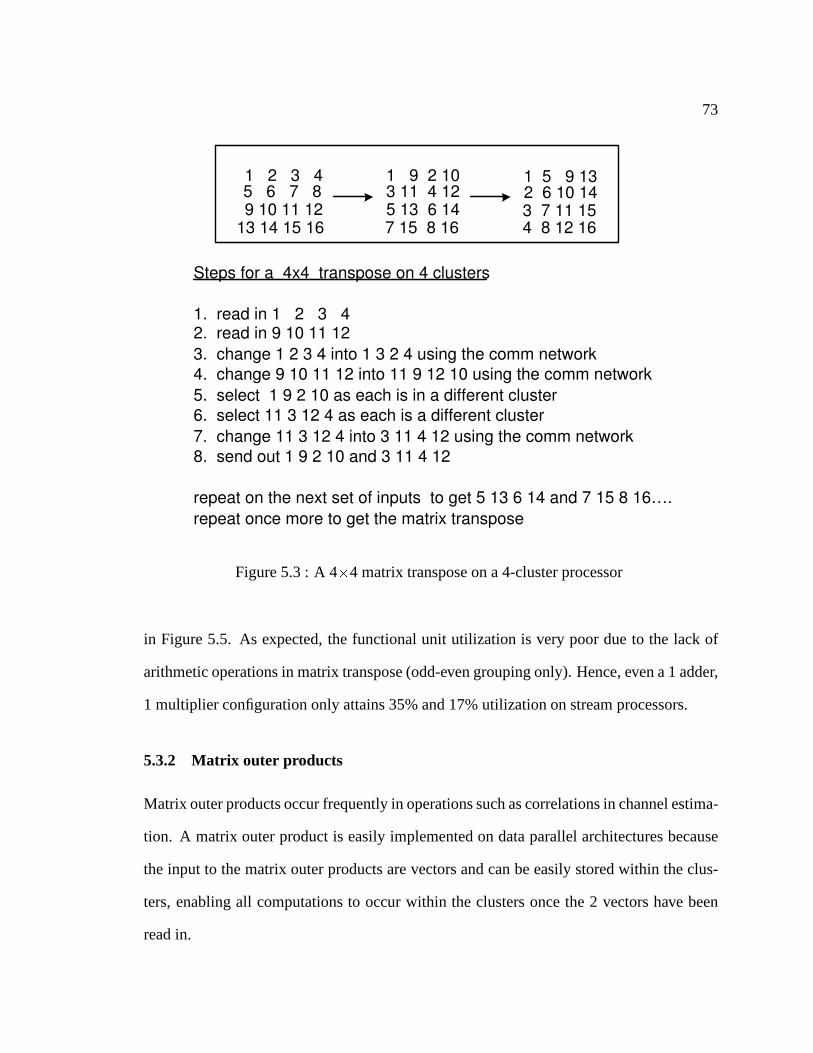
73
1 2 3 4 5 6 7 8 9 10 11 12
13 14 15 16
1 9 2 10 3 11 4 12 5 13 6 14 7 15 8 16
1 5 9 13 2 6 10 14 3 7 11 15 4 8 12 16
Steps for a 4x4 transpose on 4 clusters
1. read in 1 2 3 4 2. read in 9 10 11 12
3. change 1 2 3 4 into 1 3 2 4 using the comm network
4. change 9 10 11 12 into 11 9 12 10 using the comm network
5. select 1 9 2 10 as each is in a different cluster
6. select 11 3 12 4 as each is a different cluster
7. change 11 3 12 4 into 3 11 4 12 using the comm network
8. send out 1 9 2 10 and 3 11 4 12
repeat on the next set of inputs to get 5 13 6 14 and 7 15 8 16….
repeat once more to get the matrix transpose
Figure 5.3 : A 4�4 matrix transpose on a 4-cluster processor
in Figure 5.5. As expected, the functional unit utilizationis very poor due to the lack of
arithmetic operations in matrix transpose (odd-even grouping only). Hence, even a 1 adder,
1 multiplier configuration only attains 35% and 17% utilization on stream processors.
5.3.2 Matrix outer products
Matrix outer products occur frequently in operations such as correlations in channel estima-
tion. A matrix outer product is easily implemented on data parallel architectures because
the input to the matrix outer products are vectors and can be easily stored within the clus-
ters, enabling all computations to occur within the clusters once the 2 vectors have been
read in.

74
100
101
102
103
104
101
102
103
104
Clusters
Exe
cutio
n tim
e (c
ycle
s)
within physical cluster limitsnot physically possible
Figure 5.4 : 32x32 matrix transpose with increasing clusters
1
2
3
4
5 1
1.5
2
2.5
30.4
0.5
0.6
0.7
0.8
0.9
1
(10,1)(13,1)
#Multipliers
(10,2)
(17,1)
(13,2)
(10,3)
(19,6)
(17,2)
Auto−exploration of adders and multipliers for matrix transpose
(13,3)
(23,10)
#Adders
(19,9)
(17,3)
(23,15)
(19,17)
(35,17)
Exe
cutio
n tim
e (n
orm
aliz
ed)
with
FU
util
izat
ion
(+,*
)
Figure 5.5 : ALU utilization variation with adders and multipliers for 32x32 matrix trans-pose

75
0 10 20 30 40 50 60 70100
200
300
400
500
600
700
Clusters
Exe
cutio
n tim
e (c
ycle
s)
Figure 5.6 : Performance of a 32-length vector outer productresulting in a 32x32 matrixwith increasing clusters
Figure 5.6 shows the performance of a 32-length vector outerproduct on data parallel
architectures. The parallelism of the matrix outer productis limited by the parallelism of
the input vectors, although it is conceivable that if all theelements of 1 vector could be
broadcast to all elements of the other vector in a hypothetical architecture, the entire matrix
can be computed simultaneously. The number of operations are O(� �).Figure 5.7 shows the ALU utilization variation with adders and multipliers. While an
outer product in theory does not have any additions, incrementing the loop indices in a
software implementation cause additions. However, it is interesting to note that adding
of more than 1 arithmetic unit does not give any performance benefits for a 32-cluster
implementation as there is not sufficient instruction levelparallelism to be exploited.
5.3.3 Matrix-vector multiplication
Matrix-vector multiplications and matrix-matrix multiplications are extremely common in
advanced signal processing algorithms for wireless systems. Matrix-vector multiplications

76
1
2
3
4
5
1
1.5
2
2.5
30
0.5
1
1.5
2
#Adders#Multipliers
(49,17)
(25,49)
(25,25)
(25,17)
(17,49)(49,25)
(49,49)
(12,49)
(12,25)
(12,16)
(10,49)
(10,25)
(10,16)
(17,25)
(17,16)
Exe
cutio
n tim
e (n
orm
aliz
ed)
with
FU
util
izat
ion(
+,*
) Auto−exploration of adders and multipliers for outerproduct
Figure 5.7 : ALU utilization variation with adders and multipliers for 32-vector outer prod-uct
can be of two types�� � �
and� � �
, where the difference is the way the matrix data is
used for the computation (row-wise or column-wise). Although the data ordering does not
affect the number of arithmetic operations, it can have a significant impact on performance,
especially when implemented on a data parallel architecture.
Figure 5.8 shows the mapping of a matrix-vector multiplication on a data parallel ar-
chitecture. The vector is first loaded in the clusters and thematrix is streamed through the
clusters to produce the resulting vector. As can be seen fromFigure 5.8(a), matrix-vector
multiplication of the form� � � can be very inefficient on stream processors as the output of
the dot product of the row of a matrix with the vector results in a scalar. While computing
the dot product in a tree-based fashion on a parallel architecture, only�� �� � of the clusters
on an average, do useful work, resulting in loss in efficiency. Matrix-vector multiplication
of the form�� � � maps better on stream processors as each cluster can computean element
of the result and the dot product is iterated within a cluster, eliminating the need for inter-
cluster communication for the dot-product computation. Since�� � �
is more efficient,

77
A(i,:)
b
y(i) = A(i,:)*b
A(i,:)*b(i)
+
A(i+1,:)*b(i+1)
+
y = A H *b
=
Calculate A H
y = (A H ) H *b
(a) y = A*b (b) y = A H *b (c) y = (A H ) H *b
Figure 5.8 : Matrix-vector multiplication in data parallelarchitectures
there is an alternative way of computing� � �
as ��� �� � �, which does a matrix transpose
in the clusters as shown earlier and follows it by�� � �
.
Figure 5.9 shows the performance of the three different waysof matrix-vector compu-
tations with increasing clusters. It can be seen that the computation of�� � �provides
almost an order of magnitude better performance than the computation of� � �, demon-
strating the importance of data ordering for computations on a data parallel architecture. It
is also extremely interesting to note that the performance of� � �
does not change signif-
icantly with the number of clusters. The reason for this is that as the number of clusters
increase, the amount of work inside the kernel decreases, leading to lower ILP. Also, the
efficiency of the dot product computation decreases with increasing clusters due to the in-
crease in inter-cluster communication for the dot product computation. The third scheme,
shown in Figure 5.8(c), has a high starting overhead due to the matrix transpose being
done within the clusters, but scales well with the number of clusters, narrowly beating the
computation of� � �
.

78
100
101
102
102
103
104
Clusters
Exe
cutio
n tim
e (c
ycle
s)
A*b(AH)H*bAH*b
Figure 5.9 : Performance of a 32x32 matrix-vector multiplication with increasing clusters
5.3.4 Matrix-matrix multiplication
Matrix-matrix computation can be implemented as a matrix-vector computation over a loop
except for the fact that the matrix cannot be stored in a register as in the matrix-vector case.
Hence, both the matrices need to be streamed through the clusters for computation of the
matrix-matrix product. Also, vector elements in matrix-vector multiplications are stored
in adjacent locations, irrespective of whether the vector is treated as a row or a column
vector. This is incorrect in the case of vectors that are partof a matrix in matrix-matrix
multiplications.
Figure 5.10 shows the implementation of different forms of a32x32 matrix-matrix mul-
tiplication on stream processors. The figure shows that the standard matrix-multiplication
� � � maps well on stream processors as the elements of every row matrix � can be
broadcast to all rows of matrix� to compute the dot-product of the result without any
inter-cluster communication except broadcasting, similar to the �� � �computation in

79
100
101
102
103
104
105
Clusters
Exe
cutio
n tim
e (c
ycle
s)
A*BH
transpose(A/B) + A*BA*B
Figure 5.10 : Performance of a 32x32 matrix-matrix multiplication with increasing clusters
the matrix-vector product, where the matrix refers to� and the vector refers to the row
of matrix � . The computation of�� � � , similar to the computation of� � �requires
inter-cluster communication and has decreasing ILP with increasing clusters, providing
no benefits with increasing clusters. However, since the amount of computation to com-
munication ratio is higher in matrix-matrix multiplications, transposing the matrix� can
provide significant performance improvements as the cost ofthe matrix transpose is amor-
tized over the increase in computations. The computation ofmatrix-multiplications involv-
ing �� � � and�� � � � is more expensive in stream processors as column elements of
matrix � are required to be broadcast to the elements of matrix� . Hence, computing� � �� and
� � � for computing�� � � , and computing� � � and transposing the re-
sult for computing�� � � � are the preferred solutions for these types of matrix-matrix
multiplications.

80
5.3.5 Viterbi decoding
The Viterbi algorithm shows data parallelism in the ’add-compare-select’ operations of its
trellis. However, the data parallelism is again implicit and the trellis needs to be re-ordered
before the parallelism can be exploited by a data-parallel architecture. Figure 5.11(a) shows
the trellis structure used in Viterbi decoding. The data parallelism of the trellis is dependent
on the constraint length of the convolutional code and is exponential with the constraint
length. Hence, stronger codes (larger constraint length) exhibit more data parallelism. If we
assume that each trellis state (or a group of states in this case, as Viterbi exhibits subword
parallelism) in the vertical direction maps to a cluster, the communication between adjacent
nodes of the trellis in the horizontal direction requires inter-cluster communication. Hence,
the Viterbi trellis needs to be re-ordered between successive add-compare-select operations
as shown in Figure 5.11(b) in order to make the communicationexplicit and map to a data-
parallel architecture. The re-ordering of the data requires an odd-even grouping as can be
observed from the input and output node labels in the shuffledtrellis.
The traceback in Viterbi decoding to parse the survivor states and recover the decoded
bits is sequential and uses pointer-based addressing in order to decode the data. Hence,
traceback in Viterbi is not suitable for implementation on adata-parallel architecture. How-
ever, the surviving states can be updated and the decoded bits recovered using an alternative
approach, based on register exchange [7]. In register exchange, the register for a given node
contains the information bits associated with the surviving partial path that terminates at
that node. This is shown in Figure 5.12. The figure shows the register contents during de-
coding. Only the surviving paths have been drawn, for clarity. As the decoding operation
proceeds, the contents of the registers are updated and exchanged. The register exchange
method structure looks exactly the same as the add-compare-select operation structure and
hence, can exploit data parallelism in the number of states.Thus, the same odd-even group-

81
X(0)
X(2)
X(4)
X(6)
X(8)
X(10)
X(12)
X(14)
X(1)
X(3)
X(5)
X(7)
X(9)
X(11)
X(13)
X(15)
X(0)
X(1)
X(2)
X(3)
X(4)
X(5)
X(6)
X(7)
X(8)
X(9)
X(10)
X(11)
X(12)
X(13)
X(14)
X(15)
b. Shuffled Trellis
X(0)
X(2)
X(4)
X(6)
X(8)
X(10)
X(12)
X(14)
X(1)
X(3)
X(5)
X(7)
X(9)
X(11)
X(13)
X(15)
X(0)
X(2)
X(4)
X(6)
X(8)
X(10)
X(12)
X(14)
X(1)
X(3)
X(5)
X(7)
X(9)
X(11)
X(13)
X(15)
X(0)
X(1)
X(2)
X(3)
X(4)
X(5)
X(6)
X(7)
X(8)
X(9)
X(10)
X(11)
X(12)
X(13)
X(14)
X(15)
X(0)
X(1)
X(2)
X(3)
X(4)
X(5)
X(6)
X(7)
X(8)
X(9)
X(10)
X(11)
X(12)
X(13)
X(14)
X(15)
b. Shuffled Trellis a. Trellis
X(0)
X(1)
X(2)
X(3)
X(4)
X(5)
X(6)
X(7)
X(8)
X(9)
X(10)
X(11)
X(12)
X(13)
X(14)
X(15)
X(0)
X(1)
X(2)
X(3)
X(4)
X(5)
X(6)
X(7)
X(8)
X(9)
X(10)
X(11)
X(12)
X(13)
X(14)
X(15)
a. Trellis
X(0)
X(1)
X(2)
X(3)
X(4)
X(5)
X(6)
X(7)
X(8)
X(9)
X(10)
X(11)
X(12)
X(13)
X(14)
X(15)
X(0)
X(1)
X(2)
X(3)
X(4)
X(5)
X(6)
X(7)
X(8)
X(9)
X(10)
X(11)
X(12)
X(13)
X(14)
X(15)
X(0)
X(1)
X(2)
X(3)
X(4)
X(5)
X(6)
X(7)
X(8)
X(9)
X(10)
X(11)
X(12)
X(13)
X(14)
X(15)
X(0)
X(1)
X(2)
X(3)
X(4)
X(5)
X(6)
X(7)
X(8)
X(9)
X(10)
X(11)
X(12)
X(13)
X(14)
X(15)
X(0)
X(1)
X(2)
X(3)
X(4)
X(5)
X(6)
X(7)
X(8)
X(9)
X(10)
X(11)
X(12)
X(13)
X(14)
X(15)
X(0)
X(1)
X(2)
X(3)
X(4)
X(5)
X(6)
X(7)
X(8)
X(9)
X(10)
X(11)
X(12)
X(13)
X(14)
X(15)
X(0)
X(1)
X(2)
X(3)
X(4)
X(5)
X(6)
X(7)
X(8)
X(9)
X(10)
X(11)
X(12)
X(13)
X(14)
X(15)
Figure 5.11 : Viterbi trellis shuffling for data parallel architectures
ing can be applied for register-exchange and map it on to a data-parallel architecture.
The number of bits that a register must store is a function of the decoding depth, which
is typically around 5 times the constraint length. Since registers in programmable architec-
tures are typically 32-bit wide, we use 2 registers per statein our current implementation in
order to provide a decoding depth of 64 so that constraint lengths of 5-9 are handled. More
registers can be added if further decoding depths are desired in the application for better
performance.

82
-
-
-
-
-
-
1
0
11
10
01
00
111
110
101
000
1011
1010
1101
1100
11011
11010
10101
10100
S3
S2
S1
S0
t = 0 t = 1 t = 2 t = 3 t = 4 t = 5
Figure 5.12 : Viterbi decoding using register-exchange [7]
The real-time performance of Viterbi decoding is shown in Figure 5.13, the perfor-
mance variation is studied with the number of clusters and the constraint lengths. It can be
seen that increasing the number of clusters provides betterperformance in the application
due to data parallelism exploitation and after the entire data parallelism has been exploited,
additional clusters do not provide any gains. For example, constraint length 9 Viterbi de-
coding shows a data parallelism of 64 since it has 256 states and can pack 4 states in a
32-bit register using subword parallelism. It is interesting to observe from the figure that
decoding for all constraint lengths show the same performance once the maximum data
parallelism is achieved.
Figure 5.14 shows the ALU utilization for Viterbi decoding with varying number of
adders and multipliers per cluster. The execution time decreases with increasing adders and
multipliers but saturates after the 3 adder, 1 multiplier configuration with a functional unit
utilization of 62% each on the adders and the multipliers. The functional unit utilization is
almost independent of the constraint length as the constraint length only changes the data
parallelism (loop iteration count) in the application.

83
100
101
102
103
104
105
Number of clusters
Exe
cutio
n tim
e (c
ycle
s)
Rate 1/2 Viterbi decoding for 32 users
Constraint length = 9Constraint length = 7Constraint length = 5
Figure 5.13 : Viterbi decoding performance for 32 users for varying constraint lengths andclusters
1
1.5
2
2.5
3
3.5
4
4.5
5
11.5
22.5
33.5
44.5
5
40
60
80
100
120
140
160
(43,58)
(39,41)
(54,59)
#Multipliers
(40,32)
(47,43)
(62,62)
(39,27)
(49,33)
(65,45)
(39,22)
(70,59)
(48,26)
(61,33)
Auto−exploration of adders and multipliers for kernel "acskc"
(50,22)
(73,41)
(80,34)
(60,26)
#Adders
(76,33)
(61,22)
(85,24)
(72,22)
(85,17)
(72,19)
(85,13)
(85,11)
Inst
ruct
ion
coun
t with
FU
util
izat
ion(
+,*
)
Figure 5.14 : ALU utilization for ’Add-Compare-Select’ kernel in Viterbi decoding

84
5.3.6 LDPC decoding
The access patterns for the bit node and check node computations in LDPC decoding shown
in Chapter 2 create bottlenecks in stream processor implementations. Although similar
access problems are faced in Viterbi decoding, the decomposable nature of the Viterbi
trellis graph made it possible for re-arranging the data with a simple odd-even data re-
ordering. Random interconnections are necessary between bit and check nodes [48] for
providing performance benefits using LDPC. The Tanner graphfor LDPC decoding is also
a connected graph (path exists from every node to any other node), making it difficult to
re-order the data for grouping and reducing inter-cluster communication.
Figure 5.15 shows an example of the access patterns needed inbit node and check node
computations for LDPC decoding. This access pattern makes data access extremely diffi-
cult for stream processors as stream processors are built for streaming ordered data without
any strides or indexed access. In order to overcome this bottleneck, researchers [92] have
very recently (2004) provided a SRF modification that allowsindexed access to the stream
register files, allowing addressing of data from different rows in the SRF. With this mod-
ification, the LDPC decoding becomes similar to the Viterbi decoding algorithm imple-
mentation shown in the previous subsection. The implementation of LDPC decoding using
indexed SRF needs considerable change to the current infrastructure and modifications to
the stream processor simulator and is hence, left as future work at this point in time.
5.3.7 Turbo decoding
Turbo decoding [32] is a competing decoding algorithm to LDPC decoding and is proposed
in extensions to the 3G standards such as the HSDPA (High Speed Downlink Packet Ac-
cess) standard, that provides a 10 Mbps downlink data rate. The turbo decoder performs
iterative decoding using two Viterbi decoders. However, the Viterbi decoders used in Turbo

85
1
2039
13
309
25
3
144
2038
519
1543
999
2
Cluster
1
Cluster
2
Cluster
C
Stream Register File
Inter-cluster communication network
Access patterns
for Bit nodes and
check nodes
stored in the SRF
Figure 5.15 : Bit and check node access pattern for LDPC decoding
decoding typically have a smaller constraint length and hence, have lower data parallelism.
Hence, alternative implementations such as running one Turbo decoder per user per cluster
should be considered. A Turbo decoder also requires the use of interleavers between data.
If the interleaver used is a block interleaver, it can be implemented as a matrix transpose.
However, if the interleaver is chosen as a random interleaver as in the HSDPA standard,
Turbo decoding suffers from the same limitations of LDPC implementations requiring ac-
cess to random memory banks. The SRF modifications for indexed access [92] would
be useful for Turbo decoding using a random interleaver as well. The thesis focused on
LDPC decoding over Turbo decoding for a potential 4G system as LDPC decoding showed
greater potential for mapping on a stream processor due to its high degree of explicit data
parallelism.

86
5.4 Tradeoffs between subword parallelism and inter-cluster commu-
nication
Subword parallelism exploitation has been a major innovation in recent microprocessor
designs [84, 85] for performance benefits in media processing that require limited bit pre-
cision (typically� � bits). However, while processing a kernel on a stream processor that
uses subword parallelism, the amount of subword parallelism on the inputs may not match
the subword parallelism of the outputs. In such cases of subword parallelism mismatches,
the output data ends up in being in the wrong cluster and hence, requires additional inter-
cluster communications in order to transfer the data to the right cluster.
Figure 5.16 shows an example where the input and output data precisions of a kernel do
not match. The example in Figure 5.16 shows a squaring of a 16-bit number that doubles
the precision due to multiplication to 32-bits�. In this case, since the input data is packed,
input data elements 1 and 2 will go to cluster 0, elements 3 and4 to cluster 1 and so on.
After multiplication, the 32-bit results of elements 1 and 2will lie in cluster 0, 3 and 4 in
cluster 1. However, the result can no longer be packed (beinga 32-bit number). Outputting
the result directly at this point implies that the output would be �� � � � � � � � � � � � instead of
�� � � � � � �. Thus, the data needs to be re-ordered within the clusters. This additional re-
ordering using inter-cluster communication can be quite expensive as shown in the example
of Figure 5.16.
For purposes of this example, we will assume a latency of 1 cycle for read and write, a
4 cycle latency on multiplication and a 2 cycle latency on inter-cluster communication and
addition. Furthermore, we will assume all units are pipelined and the compiler generates
the optimal code (shown) for this example. From the example,we can see that not having
�We will assume that we need the entire 32-bit precision at theoutput

87
1 2 3 4 5 6 7 8 a
Multiplication
1 3 5 7 p
2 4 6 8 q
1 2 3 4 p
5 6 7 8 q 7
Algorithm:
short a; int y; for(i= 1; i < 8 ; ++i)
{ y[i] = a[i]*a[i]; }
Re-ordering data
1 3 x x p
5 7 x x m
x x 2 4 n
x x 6 8 q
1 3 2 4 p
5 7 6 8 q
Packed Data (Ideal): Read 1
multiplications 5 write 6
write 7 Total: 7 cycles
Packed Data (Actual) :
Read 1 multiplications 5
comm 7 comm 8
add 9 comm 11 comm 12 write 13
write 14 Total : 14 cycles
Unpacked Data:
Read 1 Read 2
multiplications 5 multiplications 6
write 6 write 7
Total: 7 cycles
Add
Re-ordering data
Figure 5.16 : Example to demonstrate trade-offs between subword parallelism utilization(packing) and inter-cluster communication in stream processors
88
packed the data reduces the execution time by half against packed data at the expense of
twice the amount of data memory storage for the unpacked input data.
Thus, the example seeks to clarify that tradeoffs between packing and inter-cluster com-
munication should be carefully considered while mapping analgorithm on processors ex-
ploiting subword and data parallelism.
5.5 Tradeoffs between data reordering in memory and arithmetic clus-
ters
Since all applications are not perfectly data parallel, many kernels require data re-ordering
in order to place the data in the right clusters. For example,a matrix transpose requires the
data in clusters to be transposed before it can be used by a kernel. The programmer has two
choices for data re-ordering between memory and the arithmetic clusters.
Data re-ordering in memory can be pipelined with other kernels in order to provide
savings in performance as shown in Figure 5.17.
It is usually preferable to do data re-ordering in the kernels for the following reasons:
1. If the data uses subword parallelism, it is not possible todo data re-ordering in mem-
ory as all memory re-ordering operations work on 32-bit datain the stream processor.
To re-order subword data, DRAM should support subword access and this increases
the complexity of the streaming memory system controller.
2. Data re-ordering in external memory can be more than an order of magnitude expen-
sive in terms of performance. For media and communications processing, the latency
of the DRAM is less important than the DRAM bandwidth as the data pattern is
known to the programmer/compiler and can be easily pre-fetched/issued in advance.
Non-single stride accesses can decrease the DRAM bandwidth, making it more ex-

89
t 1
t 2
Transpose
t mem
ALUs Memory
t 1
t 2
Transpose
t mem
ALUs Memory
t 3
t 1
t 2
ALUs
t alu
t = t 2 + t
stalls
0 < t stalls
< t mem
(a)
t = t 2
(b)
t = t 2 + t
alu
(c)
Figure 5.17 : Example to demonstrate trade-offs between data reordering in memory andarithmetic clusters in stream processors
pensive for data re-ordering. Single stride accesses have been shown to achieve 97%
of the DRAM bandwidth while random accesses have shown to attain only up to 14%
of the DRAM bandwidth [90]. This can be seen from Figure 5.18,where a matrix
transpose is shown using re-ordering in memory vs. re-ordering inside the arithmetic
clusters. The plot shows a 32-cluster stream processor architecture and the variation
of the memory re-ordering time with the DRAM clock, varying between� and� CPU
clock cycles. The DRAM clock is assumed slower than the CPU clock as in most
microprocessors [93], the DRAM clock is a multiple of the PCIbus speed (66-133
MHz) and lags behind the CPU clock (0.3-1 GHz).
3. Re-ordering operations in memory conflicts with other memory load-store operations
and may increase the memory stalls for other kernels requiring data from memory.
4. Data re-ordering in external memory is usually more expensive in terms of power
consumption, given off-chip accesses and increased cycle time incurred during the

90
104
103
104
105
Matrix sizes (32x32, 64x64, 128x128)
Exe
cutio
n tim
e (c
ycle
s)
Transpose in memory (tmem
): DRAM 8 cyclesTranspose in memory (t
mem): DRAM 3 cycles
Transpose in ALU (talu
)
Figure 5.18 : Matrix transpose in memory vs. arithmetic clusters for a 32-cluster streamprocessor
data re-ordering.
However, as seen in Figure 5.17(b), if real-time performance is critical, then data re-
ordering may provide better performance for applications in which the data re-ordering can
be hidden in other kernels.
5.5.1 Memory stalls and functional unit utilization
While the data re-ordering operations in matrix transpose was explicit, some kernels such
as Viterbi have implicit data re-ordering, done for re-ordering the trellis states. Now, the
data re-ordering can be similarly be done in memory and in clusters. Removing the data re-
ordering from the kernel and pushing it to the memory (the reverse of matrix transpose) can
again produce similar trade-off questions and can attain performance benefits and increased
adder-multiplier utilization at the expense of increased memory stall latencies. Since we
have seen that data re-ordering in memory is usually more expensive, data re-ordering is

91
done within the kernels for algorithms having implicit datare-ordering.
5.6 Inter-cluster communication patterns in wireless systems
Future microprocessor designs are going to be communication-bound instead of capacity-
bound [94]. The wire delay has exceeded the gate delay in 0.18� technology and the effects
of inductance, capacitance and delay of wires are becoming increasingly important in mi-
croprocessor design, especially as more transistors are becoming smaller and increasing in
number with technology [95]. The number of cycles needed to communicate data between
the furthest clusters is going to increase due to the increase in wire delay. Hence, techniques
to reduce inter-cluster communication are needed to provide scaling of microprocessor de-
signs with technology. The inter-cluster communication network needs the longest length
wires in stream processors. By investigating the inter-cluster communication patterns for
all the wireless kernels investigated, we note that although the inter-cluster network is fully
connected in stream processors, we use only 2 operations in the inter-cluster communica-
tion network in wireless applications.
1. odd-even grouping(shown by packing, transpose and Viterbi algorithms)
2. broadcasting 1 cluster to all clusters(shown in matrix-based computations)
This can be achieved via a single 32-bit interconnection busover all clusters, decreas-
ing the wire length by���
� �� �, and decreasing the interconnections of the inter-cluster
communication network by the number of clusters. More importantly, it allows greater
scaling of the inter-cluster communication network with the number of clusters as all inter-
connections are only nearest neighbor connections. Odd-even grouping can be achieved in
8 cycles by adding a specialized network that loads the first data, loads the second data in
the next cycle and then outputs the odd and even data in consecutive cycles. Broadcasting

92
can be done in 2 cycles by storing the clusters’ output in a register the first cycle and then
broadcasting it in the second cycle. This reduced inter-cluster communication network is
shown in Figure 5.19. As can be seen from Figure 5.19(a), if data transfer between the fur-
thest clusters (0 and 3 in this case) will limit the cycle time(and clock frequency) due to the
wire length and due to the parasitic load effects caused due to the inter-connections. The
reduction in wire length by���
� �� �, the reduction in the number of interconnections by�
and the use of neighboring interconnects only allows greater scaling of the inter-connection
network with the number of clusters in the stream processor.This relates back to the overall
lwo power improvements to stream processors proposed in Chapter 4 (Figure 4.10).
The broadcasting support from 1 cluster to all clusters allows complete distribution of
data to all clusters. The data can then be matched with the processor id to decide whether
the data is useful or not. However, this may increase the latency for random inter-cluster
data movement by the number of clusters.
5.7 Stream processor performance for 2G,3G,4G systems
Figure 5.20 shows the performance of stream processors for afully loaded 2G and 3G
base-station with 32 users at 128 Kbps and 16 Kbps respectively. The architecture as-
sumes sufficient memory in the SRF to avoid accesses to external memory (256 KB) and
3 adders and 3 multipliers per cluster (chosen because matrix algorithms tend to use equal
number of adders and multipliers). For our implementation of a fully loaded base-station,
the parallelism available for channel estimation and detection is limited by the number of
users while for decoding, it is limited by the constraint length (as the users are processed
sequentially).
Ideally, we would like to exploit all the available parallelism in the algorithms as that
would lower the clock frequency. Having a lower clock frequency has also been shown

93
0/4 1/5 2/6 3/7
4 Clusters
Inter-cluster
communication
Operation Cycle(Start,End)
Input : 0 1 2 3 :1 1
Input : 4 5 6 7 :2 2
Comm: 0 2 1 3 :2 3
Comm: 5 7 4 6 :3 4
Output : 0 2 4 6 :5 5
5 7 1 3 :4 5
Comm: 1 3 5 7 :6 7
Output: 1 3 5 7 :7 8
Total : 8 cycles
(a) Odd-even grouping on the default inter-cluster communication network
O(C 2 ) wires, O(C 2 ) interconnections, 8 cycles
Data
0/4 1/5 2/6 3/7
Broadcasting
support
Odd-even
grouping
Registers
(pipelining)
Multiplexer
4 Clusters
Demultiplexer
Operation Cycle(Start,End)
Input : 0 1 2 3 :1 1
Input : 4 5 6 7 :2 2
Comm: 0 2 4 6 1 3 5 7 :3 6
Output : 0 2 4 6 :6 7
Output: 1 3 5 7 :7 8
Total : 8 cycles
(a) Odd-even grouping on the modified inter-cluster communication network
with only nearest neighbor interconnections
O(C log(C) ) wires, O(C ) interconnections, 8 cycles
Data
Inter-cluster
communication
with only
nearest
neighbor
connections
Figure 5.19 : A reduced inter-cluster communication network with only nearest neighborconnections for odd-even grouping

94
100
101
102
101
102
103
104
105
Number of clusters
Fre
quen
cy n
eede
d to
atta
in r
eal−
time
(in M
Hz)
3G base−station (128 Kbps/user)3G base−station (C64x TI DSP)2G base−station (16 Kbps/user)2G base−station (C64x TI DSP)
Figure 5.20 : Real-time performance of stream processors for 2G and 3G fully loadedbase-stations
to be power efficient as it opens up the possibilities of reducing the voltage [96], thereby
reducing the effective power consumption (� � � � ). While Viterbi at constraint length 9
has sufficient parallelism to support up to 64 clusters at full load, channel estimation and
detection algorithms do not benefit from extra clusters, having exhausted their parallelism.
The mapping of a smaller size problem to a larger cluster sizealso gets complicated because
the algorithm mapping has to be adapted by some means either in software or in hardware
to use lower number of clusters while the data is spread across the entire SRF.
From the figure, we can see that a 32-cluster architecture canoperate as a 2G base-
station at around 78 MHz and as a 3G base-station around 935 MHz, thereby validating
the suitability of Imagine as a viable architecture for 3G base-station processing. It is also
possible that other multi-DSP architectures such as [97] can be adapted and are viable for
3G base-station processing. However, the lack of multi-DSPsimulators and tools limit our
evaluation of these systems.
The use of an indexed SRF [92] is required for implementing a LDPC decoder on stream

95
processors. Since the current tools did not support this capability, a detailed implementa-
tion of a 4G system was not considered. However, this will affect only the SRF access
performance and will require modifications only to the streamC code. The next chapter
shows the expected performance of a 4G system based on a kernelC implementation and
using an estimate for memory stalls.
5.8 Summary
This chapter shows that, in spite of algorithms having abundant data parallelism, algo-
rithms need to be modified in order to map efficiently on streamprocessors. This is be-
cause the data that can be processed in parallel is not necessarily aligned to the DSP cluster
utilizing that data. Hence, expensive inter-cluster communication operations or memory
re-ordering operations are required to bring the data to theright cluster before it can be uti-
lized. This creates trade-offs between utilization of subword parallelism, memory access
patterns and execution time. This thesis finds that the algorithms implemented in this thesis
can be designed to use only two inter-cluster communicationpatterns. Hence, a special-
ized inter-cluster communication network can be used to replace the general inter-cluster
communication network, reducing the DSP complexity and providing greater scalability of
the design with increasing clusters. This chapter thus demonstrates the benefits of a joint
algorithm-architecture design for efficient algorithm mapping and architecture complexity
reduction. The next chapter 6 presents the trade-offs in deciding the number of arithmetic
units and the clock frequency in order to meet real-time requirements with minimum power
consumption and chapter 7 shows how the designed architecture can then adapt to varia-
tions in the workload for improved power-efficiency.

96
Chapter 6
Design space exploration for stream processors
6.1 Motivation
Progress in processor technology and increasing consumer demand have brought in inter-
esting possibilities for embedded processors in a variety of platforms. Embedded proces-
sors are now being applied in real-time, high performance, digital signal processing appli-
cations such as video, image processing and wireless communications. The application of
programmable processors in high performance and real-timeembedded applications poses
new challenges for embedded system designers. Although programmable embedded pro-
cessors trade flexibility for power-efficiency with custom solutions, power awareness is an
important goal in embedded processor designs. Given a workload with a certain real-time
design constraint, there is no clear methodology on designing an embedded stream pro-
cessor that meets performance requirements and provides power efficiency. The number
of clusters in the stream processor, the number of arithmetic units and the clock frequency
– each can be varied to meet real-time constraints but can have a significant variation in
power consumption.
An exhaustive simulation for exploration is limited by the large architecture parameter
exploration space [98] and limitations of compilers for stream processors [99], necessi-
tating hand optimizations for performance. Efficient design exploration tools are needed
to restrict the range of detailed simulations to a finite and small subset, depending on the
available compute resources and the simulation time. Moreover, embedded systems such

97
as wireless are evolving rapidly [10, 100]. The designer needs to evaluate a variety of can-
didate algorithms for future systems and would like to get a quick estimate of the lowest
power embedded processor that meets real-time for each of his candidate algorithms. This
thesis provides a tool to explore the choice of ALUs within each cluster, the number of
clusters and the clock frequency that will minimize the power consumption of a stream
processor. Our design methodology relates the instructionlevel parallelism, subword par-
allelism and data parallelism to the organization of the ALUs in an embedded stream pro-
cessor. The thesis exploits the relationship between thesethree parallelism levels and the
stream processor organization to decouple the joint exploration of the number of clusters
and the number of ALUs within each cluster, providing a drastic reduction in the design
space exploration and in programming effort. The design exploration methodology also
provides insights to the functional unit utilization of theprocessor. The design exploration
tool exploits the static nature of signal processing workloads to provide candidate config-
urations for low power along with an estimate of their real-time performance. Our design
exploration tool also automates machine description exploration and ALU efficiency calcu-
lation at compile time. A sensitivity analysis of the designto the technology and modeling
enables the designer to check the robustness of the design exploration. Once the design
exploration tool churns out candidate configurations, detailed simulations can then be per-
formed for those configurations to ensure that the design meets the specifications.
Similar challenges are faced by designers implementing algorithms on FPGAs [101].
Most FPGA tool vendors such as Xilinx, allow multiple levelsof design verification and
timing closure in their design tools. The aim is to allow a fast functional verification fol-
lowed by detailed timing analysis and using successive refinements to attain timing closure.

98
6.1.1 Related work
The combination of completely programmable solutions along with the need for high per-
formance presents new challenges for the embedded system designers, who have tradition-
ally focused on exploring heterogeneous solutions to find the best flexibility, performance
and power trade-offs [50]. Design space exploration has been studied for VLIW-based em-
bedded processors [67, 102] for performance and power. These techniques directly relate to
a design exploration for a single cluster stream processor.However, exploring the number
of clusters in the design adds an additional dimension to thesearch space. It is not clear as
to how to partition the arithmetic units into clusters and the number of arithmetic units to be
put within each cluster. Design space exploration has also been studied for on-chip MIMD
multiprocessors based on linear programming methods [103]to find the right number of
processors (clusters) for performance and energy constraints, assuming a fixed configura-
tion for parameters within a cluster. The design space exploration using these techniques
for stream processors need a more exhaustive and complex search for simultaneous opti-
mization for the number of clusters and the number and type ofarithmetic units within a
cluster. The tradeoffs that exist between exploiting ILP within a cluster and across clusters
increases the complexity of the design exploration. The thesis shows that the explicit use of
data parallelism across clusters in a stream processor can be exploited to provide a simpler
method to find the right number of clusters and the number and types of arithmetic units
within a cluster.
6.2 Design exploration framework
This thesis presents a design space exploration tool heuristic based on two important ob-
servations.
Observation 6.1 Signal processing workloads are compute-bound and their performance

99
can be predicted at compile-time.
The execution time of signal processing workloads is fairlypredictable at compile time
due to the static nature of signal processing workloads. Figure 6.1 shows the execution
time for a workload being composed of two parts: computations ����� � ��, and stalls���� ��.The processor clock frequency needed to attain real-time isdirectly proportional to the ex-
ecution time and we will use frequency instead of time in the analysis in the rest of the
thesis. The memory stalls are difficult to predict at compiletime as the exact area of over-
lap between memory operations and computations is determined only at run-time. The
microcontroller stalls depend on the data bandwidth required by the arithmetic units in the
clusters and vary with the algorithms, the number of clusters and the availability of the data
in internal memory. Some parts of the memory and microcontroller stalls are constant due
to internal memory size limitations or bank conflicts and do not change with the compu-
tations. As the computation time decreases due to addition of arithmetic units (since we
are compute-bound), some of the memory stalls start gettingexposed and are thus, variable
with����� � ��. The real-time frequency needed to account for constant memory stalls that
do not change with computations is denoted by������. The worst-case memory stalls,
�� ��occurs when the entire ILP, DP and SubP are exploited in the processor, which changes the
problem from compute bound to memory bound. Hence, the memory stall time is bounded
by������ and
�� �� .
� � ����� � ��� �
��� �� � ���� ���� �� ����� �� �
�� �� (6.1)
It is interesting to note the increase in memory stalls with lower clock frequencies. In
a traditional microprocessor system with a constant configuration, the memory stalls tends
to decrease with lower clock frequencies of the processor since the caches have more time

100
Computations
Hidden memory
stalls
Exposed
memory stalls
Total
Execution Time
(cycles)
Microcontroller
stalls
t compute
t mem
t stall
Figure 6.1 : Breakdown of the real-time frequency (execution time) of a workload
now to get data from external memory. However, in this case, the number of clusters in the
stream processor are increasing to decrease the clock frequency while keeping the memory
bandwidth the same. This implies that the memory now has to source more data to the
SRFs at the same bandwidth, thereby increasing the number ofstalls in the architecture.
Definition 6.1 Data Parallelism(DP) can be defined as the number of data elements that
require the exact same operations to be performed in an algorithm and is architecture-
independent. In this thesis, we define a new term,cluster data parallelism (CDP� DP),
as the parallelism available in the data after exploiting SubP and ILP. Thus, cluster data
parallelism is the maximum DP that can be exploited across clusters without significant
decrease in ILP or SubP.

101
ILP exploitation within a cluster is limited due to finite resources within a cluster such
as finite register sizes, inter-cluster communication bottlenecks and finite number of input
read and output write ports. Increasing some of the resources such as register file sizes are
less expensive than adding an extra inter-cluster communication network [23], which can
cause a significant impact on the chip wiring layout and powerconsumption. Any one of
these bottlenecks is sufficient to restrict the ILP. Also, exploiting ILP across basic blocks
in applications with multiple loops is limited due to the compiler [99]. Signal processing
algorithms tend to have significant amounts of data parallelism [10, 22, 23, 104]. Hence,
DP is available even after exploiting ILP, and can be used to set the number of clusters as
CDP.
Observation 6.2 Due to limited resources within a cluster, not all DP can be exploited as
ILP in stream processors via loop unrolling. The unutilizedDP can be exploited across
clusters as CDP.
This observation allows us set the number of clusters according to the CDP and set
the ALUs within the clusters based on ILP and SubP, decoupling the problem of a joint
exploration of clusters and ALUs within a cluster into independent problems. This provides
a drastic reduction in the exploration space and in programming effort for various cluster
configurations. The observation is best demonstrated by an example of the Viterbi decoding
algorithm used in wireless communication systems.
Figure 6.2 shows the performance of Viterbi decoding with increasing clusters in the
processor for�� users done sequentially, assuming a constant cluster configuration of �adders and� multipliers in a cluster. The data parallelism in Viterbi decoding is propor-
tional to the constraint length,� , which is related to the strength of the error control code.
A constraint length� Viterbi decoder has��� � �� states, and hence has DP of��,

102
100
101
102
103
104
105
Number of clusters
Exe
cutio
n tim
e (c
ycle
s)
Rate 1/2 Viterbi decoding for 32 users
Constraint length = 9Constraint length = 7Constraint length = 5
Figure 6.2 : Viterbi decoding performance for varying constraint lengths and clusters
and can use 8-bit precision to pack 4 states in one cluster (SubP� ), reducing the CDP
to � �� � . Hence, increasing the number of clusters beyond does not provide per-
formance benefits. However, as the clusters reduce from to for � � �, there is an
almost linear relationship between clusters and executiontime, showing that the ILP and
SubP being exploited can be approximated as being independent of the CDP. The deviation
of the performance curve with clusters from a slope of�
� represents the variation of ILP
with CDP.
This thesis bases the design exploration framework on the two assumptions that were
discussed in this section.
6.2.1 Mathematical modeling
Let the workload� , consist of� algorithm kernels executed sequentially on the data-
parallel stream processor; given by �, �, ... , . Let the functional units in the embedded
processor be assumed to solely adders and multipliers, for the purpose of this analysis. Let

103
the respective execution time of the kernels be� � �� � � � ��, �� �� � � � ��, ...,� �� � � � ��, where
(�,� ,�) be the number of adders per cluster, the number of multipliers per cluster and the
number of clusters respectively. Let the cluster data parallelism in each of these kernels be
defined as��� �, ��� �, ,��� .
Figure 6.3 explains the design framework proposed for data-parallel embedded stream
processors. The design phase consists of a worst-case workload that needs to be designed
to meet real-time constraints in a programmable architecture. The exploration tool then
searches for the best (� � � � � � � ) configuration that minimizes the power consumption of
the processor for that workload. Once the chip is designed, the architecture can run the
workload as well as other application workloads by dynamically adapting (� � � � � � � � � )
parameters to match that of the application. Thus, the solution provides possibilities for
using this designed architecture for investigating run-time variations in the workload and
adapting to the variations.
Our design goal is to find (�,� ,�) and the real-time frequency,�, such that the power
� �� �� ��� is minimized.
� ��� �� �� �� � � � ��� �� �� �� � �� � � � ��� �� �� � � � �� (6.2)
where� �� � � � �� is the loading capacitance,
�is the supply voltage and
� �� � � � �� is the
clock frequency need to meet real-time requirements. The model for the capacitance is
derived from the Imagine stream processor implementation and is presented in the next
section.
The power consumption of the DSP is also dependent on the average switching activity
in the DSP. However, the switching activity can be related tothe functional unit utilization,
which in turn can be related to the execution time. However, parts of the chip such as

104
Base data-parallel
stream processor
Design
Workload
Application
Workload
Explore (a,m,c,f)
combination that
minimizes power
Dynamic adaptation
to turn down (a,m,c,f,V)
to save power
Hardware
Implementation
+ + + * * *
+ + + * * *
+ + + * * *
Figure 6.3 : Design exploration framework for embedded stream processors
the stream register file and the microcontroller can still beassumed to have a fairly con-
stant switching activity. Since the design exploration tries to provide solutions having high
functional utilization as well as low execution time, the switching activity variations are
assumed to not significantly affect the design decisions andare hence, currently assumed
to be constant in the design exploration.

105
6.2.2 Capacitance model for stream processors
To estimate the capacitance, we use the derivation for energy of a stream processor from
[23], which is based on the capacitance values extracted from the Imagine stream proces-
sor fabrication. The equations in [23] have been modified to relate to the calculation of� �� � � � �� in this thesis instead of energy in [23]. Also, the equationsnow consider adders
and multipliers as separate ALUs instead of a global ALU as considered in [23]. The model
does not consider the static power dissipation in the processor. The static power dissipa-
tion is directly proportional to the number of transistors and hence, the capacitance [105].
The static power dissipation is also a function of leakage effects of transistors and varies
with technology. Static power dissipation does not affect the minimization and choice of
�� � � � �� , although it will affect the actual power number that is output from the model
for a given technology. The model can be improved by adding a static power consumption
factor based on [105] in the cost function for the optimization.
The thesis first describes the parameters used in the derivation, which is shown in Table
6.1. The following equations are then used to calculate the capacitance model for the
design exploration. For simplicity, we ignore the�� � � � �� subscripts in the capacitances�
and areas�
below, except for the final� �� � � � �� in equation (6.3). The capacitance
� �� � � � �� is composed of the capacitance of the stream register file�
���
(per cluster),
the capacitance of the inter-cluster communication network� �
� ���
(per cluster), the cluster
capacitance� ���� and the micro-controller capacitance
�� �.

106
Parameter Value Description����� 16.1 Area of 1 bit SRAM used for SRF or microcontroller (grids)���
230.3 Area per stream buffer (SB) width (grids)�� � ���� ���� 515 Datapath width of a multiplier (tracks)�
�� �
92.1 Datapath width of 2 LRFs (tracks)��� 1551 Scratchpad datapath width�
640 Datapath height for all cluster components�� 1 Normalized wire propagation capacitance per wire track��� ���� ���� 6.3e+5 Cap. of ALU operation (normalized to
�� )����� 8.7 SRAM access cap. per bit (normalized to
�� )���
155 Cap. of 1 bit of Stream Buffer (SB) access (normalized to�� )�
�� �
7.9e+4 Local reg. file cap.(normalized to�� )�
�� 1.6e+6 Scratchpad cap. (normalized to�� )�
55 Memory latency (cycles)�32 Data width of the architecture�
�� �
0.5 Width of SRF bank per N (words)���
0.2 Average number of SB accesses per ALU operation in typical kernels� ���� 0.2 COMM units required per N��� 0.2 SP units required per N�� 196 Initial width of VLIW instructions (bits)�� 40 Additional width of VLIW instructions per� �
� � 6 Initial number of cluster SBs� 6 Required number of non-cluster SBs� 0.2 Additional SBs required per N� 20 SRF capacity needed per ALU for each cycle of memory latency (words)�� 2048 Number of VLIW instructions required in microcode storage
� �� � � a + m Number of ALUs per cluster� 0.1,0.01 ratio of adder to multiplier cap. (power)� ����� 155 datapath width of an adder (tracks)
Table 6.1 : Summary of parameters

107
� �� � �� � �� � � � �� �
� � � � � ���� � ����� �� � ��� �� ��
� � (6.3)� �� ��
� � �� ����� ��� ����� �
�� � � � ���� ���� (6.4)� ���� � � �
� �� � �� �� � � � �� � ��� �� � �� �� �� � �� ��� � �
� �� � ��� �� ��� (6.5)
�� �� � ������� � ��� � ���� ����
� �� � � (6.6)������ � ���� ��
�� ���� (6.7)�
�� � �� ��� � �
�� �� �� � ��� �
��� ����� �
� �� � ���� ��� ���� �� � � �� ����
� � ���� �� (6.8)
��� � � � � � �� � ��� �
������
��� � � �
��� �� � �� �� �
� � � �� ���� � (6.9)
� �� ��� � �� ��� �
� �� � � �� � ��� �� �� � ��� �
��� �� �� � � �� � �� �� � � � �
�� � � �� �
� �� � ���� (6.10)
� ���� �� � � � � ����� �� � � (6.11)
� �� �� � � � ���� �� � � (6.12)
� �� �� � � � � �� � � � � �� �� � � � � ���� �� � � (6.13)
� � ��� �� � � � � � �� �� � � (6.14)
� �� �� � � �
�� � � ��� �� � � (6.15)
� � �� �� � � � �� ����� � ���� ���� ����
� (6.16)�
�� � � � � � �� � �� �
��� � � �� �� �� �� � �� �
� �� � �� �� �
(6.17)�
�� � � �� �� � ���� �
� �� � ��� ���� �� �� � �� � � � �� � �� �� � � � �� �
� � � ��� �
� �� � � ���� �� �� � �� � � � � � �� � �
�� � �� ���� �� � �� (6.18)
� ���� � � �� �� � �� �
�� � � � � � �� �� � �� � � �� �� � �� ��� � �
�� (6.19)� ���� � �� ���� �� � ���� �� ���� �� � ���� � ��� � ���� �
�� � � (6.20)�
�� � �� � ��� � �
�� �� �� � ��� �
��� � ���� �� �� � ����
��� � � ����
� � ���� (6.21)
Thus, by varying� � � � �, the change in the capacitance� �� � � � �� can be calculated
and used in the design exploration. The processor clock frequency is dependent on the
processor voltage as follows:
� �� �
�
���
� (6.22)
where�
� is the threshold voltage [106]. Now, to achieve a real-time frequency�, the

108
processor voltage also needs to be set accordingly. Hence, from equations (6.2) and (6.22),
we get
���� �� �� � � ���� �� �� � �� � � � ��� ��� �� ��� (6.23)
The design space exploration tool shown in the next section optimizes equation (6.23) to
find the number and organization of the arithmetic units thatminimize the power consump-
tion.
6.2.3 Sensitivity analysis
As transistors have gone towards the deep-submicron regime, the transistors are getting
shorter and saturating at lower drain-to-source voltages [105]. The relationship between the
drain current and the gate-to-source voltage has gone down from quadratic to linear [107].
This has affected the delay variation in the transistor withvoltage from being quadratic as
shown in equation (6.23) to being linear with voltage.
Hence, the power equations are going down from being cubic toquadratic. Decreasing
the threshold voltage helps but the trends still continue asthe threshold voltage cannot
be decreased at the same rate as the drain-to-source voltage[105]. The actual number is
very much technology dependent. Hence, to analyze the sensitivity of the design to the
technology, we assume,
� � �
� ��� � �� � � � �� (6.24)
� ��� �� �� � � ���� �� �� � �� � � � ��� ��� �� ��� (6.25)
� ���� �� � � � ��
This model can be thus generalized to allow the designer to set the number for� , plug it in
and minimize the equation to design the architecture.

109
Similarly, functional units in an actual physical realization can have different power
consumption values than those used in a power model. If we assume 2 types of functional
units such as adders and multipliers in the design, we need tomodel the power consumption
of one relative to the other to make the values used independent of the technologies and
actual implementations. The power consumption of adders are linear with the bit-width�
and the multiplier power consumptions are quadratic with the bit-width [108]. Hence, in the
thesis, using equally aggressive 32-bit adders and multipliers, we will assume variations in
adder power to be between� � � and� � of the multiplier power. As will be seen later, this
variation is not important as the additional register files and the intra-cluster communication
network that gets added with the functional units dominate the power consumption instead
of the functional units by themselves.
������ � � �� � (6.26)
�� � ���� ���� � � ��� � (6.27)
������ � � � ��� ���� ���� (6.28)
� ���� �� � � � � � � ��
The organization of the stream processor provides a bandwidth hierarchy, which al-
lows prefetching of data and mitigates memory stalls in the stream processor [104, 109].
Memory stalls have been shown to account for� � �% of the total execution time in me-
dia processing workloads [109] and��% of the execution time in wireless communication
workloads [100]. Stalls are caused in stream processors dueto waits for memory transfers
(both external memory and microcontroller stalls), inefficiencies in software pipelining of
the code, and time taken to dispatch microcontroller code from the host processor to the
microcontroller [109]. In order to model memory stalls and observe the sensitivity of the

110
design to the stalls, we model the worst-case stall�� �� to be��% of the workload at the
minimum clock frequency that is needed for real-time� � �� �� where the entire available
ILP, DP and SubP are exploited. This thesis model variationsin memory and microcon-
troller stalls using a parameter� between� and � to explore the sensitivity of the design
tools to the stalls. Hence, from equation (6.1),
���� �� � �� � � ��� �� � ���� �� � � � �� (6.29)
���� �� � � �� �� � � ��� �� (6.30)
� � � represents the no-stall case and� � � represents the worst-case memory stall�� �� . The minimum real-time frequency,
�� �� , is computed during the design exploration.
There are other parameters in an embedded stream processor that can affect performance
and need exploration such as the number of registers and pipelining depth of ALUs [67,
98, 102]. These parameters affect the ILP for a cluster and hence, indirectly affect the
CDP. Although an exploration for these parameters will affect the actual choice for the
design, the design exploration methodology does not changeas we decouple ILP and DP
in our design exploration. In order to stress the design methodology and our contributions,
we focus on the exploration of�� � � � � � � � for power minimization and their sensitivity to
three parameters:�� � � � � �. Once�� � � � � � � � have been decided, other parameters can be
set based on this configuration.
6.3 Design space exploration
The thesis starts the design exploration with an over-provisioned hypothetical architecture,
having infinite clusters and infinite ALUs within each cluster. This point is then revised by
decreasing clusters and ALUs to find smaller configurations until the real-time frequency
begins to increase. This revised architecture configuration still exploits all the possible ILP,

111
SubP and DP available in the algorithms and is given by (���� ,���� ,��� ���� �). From
this point on, we explore trade-offs between frequency and capacitance in equation (6.25)
to find the configuration that attains real-time at the lowestpower.
6.3.1 Setting the number of clusters
To find the number of clusters needed, we compile all kernels at their maximum CDP levels,
assuming a sufficiently large number of adders and multipliers per cluster. The thesis then
runs kernel with (���� � ���� � ��� �) where ���� � ���� are a sufficiently large enough
number of adders and multipliers per cluster to exploit the available ILP in all kernels. The
compile-time execution for kernel is given by�� ������ ����� ���� � �.Hence, the real-time frequency
� �� � � � �� is given by
� �� �� ���(MHz) � Real-time target(Mbps) * Execution time per bit(a,m,c) (6.31)
�� �� � Real-time target * Execution time per bit(���� � ���� �max���� �)(6.32)
� ����� ����� ��� � ���� �� � Real-time target�
��� � ���� �� � �� ����� ����� ���� � � (6.33)
Equation (6.33) reduces the frequency by half with cluster doubling based on the obser-
vation of linear benefits of frequency with clusters within the CDP range. It also shows
that if the number of clusters chosen are greater than the available CDP, then there is no
reduction in execution time. The���� �� term accounts for stalls in the execution time that
are not predicted at compile-time, and is computed using equations (6.32) and (6.1). The
number of clusters that minimizes the power consumption is given by
���� �� � ����� ����� �� �� � � � ��� �� � ��� �� � ���� � ��� �
����� ����� ��� (6.34)
Thus, by computing� ����� ����� ���� � at compile time and plotting this function for the
desired range of clusters and for varying� , the number of clusters that will minimize the

112
power consumption is determined. The choice of clusters is independent of� as it gets
factored out in the minimization of equation (6.34).
6.3.2 Setting the number of ALUs per cluster
Once the number of clusters� is set, the number of ALUs within each cluster needs to be
decided. The number of adders and multipliers are now variedfrom ��� �� to ����� � ���� �to find the trade-off point that minimizes the power consumption of the processor. The
design tool can handle varying ALUs without any changes in the application code. Hence,
an exhaustive compile-time search can be now done within this constrained space to find
the right number of adders and multipliers that meets real-time with minimum power con-
sumption. The power minimization is now done using
���� �� �� � �� �� �� �� � � ���� �� �� � �� � � � ��� �
�� �� ��� (6.35)
The design tool also provides information about ALU efficiencies based on the schedule.
It can be shown that this power minimization is related to maximization of the ALU uti-
lization, providing us with insights about the relation between power minimization and the
ALU utilization. The choice of ALUs inside a cluster is dependent on�, � and� .
6.3.3 Relation between power minimization and functional unit efficiency
The power minimization methodology discussed above also provides us with insights into
the functional unit utilization of the embedded processor.In order to explore this, let us
consider the multiplier as a sample functional unit and let us assume the other parameters
(adders and clusters) as constant.

113
���� � �� � � ����� �� �� �
�� � (6.36)
���� � �� � � � ����
� �� �� �
�� � (6.37)
� � ���� �
� �� �� �
�� � (6.38)
where�
is the total number of multiplications occurring in the workload which is a con-
stant.
���� � �� � � � ���� �
� �� �� �
� � � �
�� � (6.39)
� � ���� �
� �� �� �
� � �� � ��
(6.40)
Since the frequency�
needed to meet real-time is directly proportional to the execution
time, the number of multiplications divided by the total number of multipliers and the
frequency is directly proportional to the multiplier utilization,�
� ���.
� ��� � �� � � � ���� �
� �� �� �
� ��� (6.41)
� � ����
� �� � �� � � ��� (6.42)
Thus, we can see that the power minimization is directly related to maximization of a
scaled version of the functional unit utilization. The relation derived here is based purely
on the power minimization model and is independent of the actual architecture. The exact
relation between� �� � and� for the embedded stream processor can be obtained from the
equations in the appendix. To a first level approximation,� �� � can be assumed to be linear
with � , although there are secondary terms present due to the intra-cluster communication
network. This is a useful result as we now know that in addition to power minimization,

114
the exploration also maximizes functional unit efficiency in some manner, which should be
expected of any power minimization based design exploration.
6.4 Results
For evaluation of the design exploration methodology, the design concept was applied
for designing a�� wireless base-station embedded processor that meets real-time re-
quirements. For the purposes of this thesis, we consider a��-user base-station with���Kbps/user (coded), employing multiuser channel estimation, multiuser detection and Viterbi
decoding [10, 100]. This was considered to be the worst-caseworkload that the processor
needed to support in the design.
The design boundary conditions used for the workload are shown in Table 6.2. Ideally,
the CDP range should be decided by the exploration tool with the help of the compiler. The
compiler should automatically exploit all the available ILP (using loop unrolling) and SubP
and set the remaining DP as CDP. In the absence of the compiler’s ability to automate this
process, the CDP has been set manually after exploring different amounts of loop unrolling
and finding out the changes in ILP. The cluster configuration is varied up to��� clusters
as that is the maximum CDP available. Similarly, the adders and multipliers are varied up
to � and� respectively as we have seen ILP saturating above these configurations with no
benefits in performance. These ranges will be confirmed in thedesign exploration process.
Table 6.3 shows the break-up of the workload computations for attaining the lowest
real-time frequency that is obtained at compile-time usingequation (6.32). The CDP varies
in the algorithms between�� and ���, justifying the range for CDP exploration in Table
6.2. Also note that since� ��% of the real-time frequency is needed due to kernels that
require�� and clusters, there is little advantage in exploring a higher number of clusters.
The minimum real-time frequency needed�� �� is estimated to be��� MHz for the design

115
Parameter Min Max
CDP range �� ���� ���� � �� � �
Table 6.2 : Design parameters for architecture explorationand wireless system workload
100
101
102
103
102
103
104
Clusters
Fre
quen
cy (
MH
z)
β = 0β = 0.5β = 1
Figure 6.4 : Variation of real-time frequency with increasing clusters
workload.
Figure 6.4 shows the real-time frequency of the workload with increasing clusters as
� is varied, using equations (6.33). Since the minimum CDP is��, the execution time
decreases linearly until�� and then no longer provides a linear decrease as seen from
equation (6.33). Further increasing the clusters above clusters has almost no effect
on the execution time as the algorithms using the higher CDP take less than�% of the
workload time, as shown in Table 6.3.
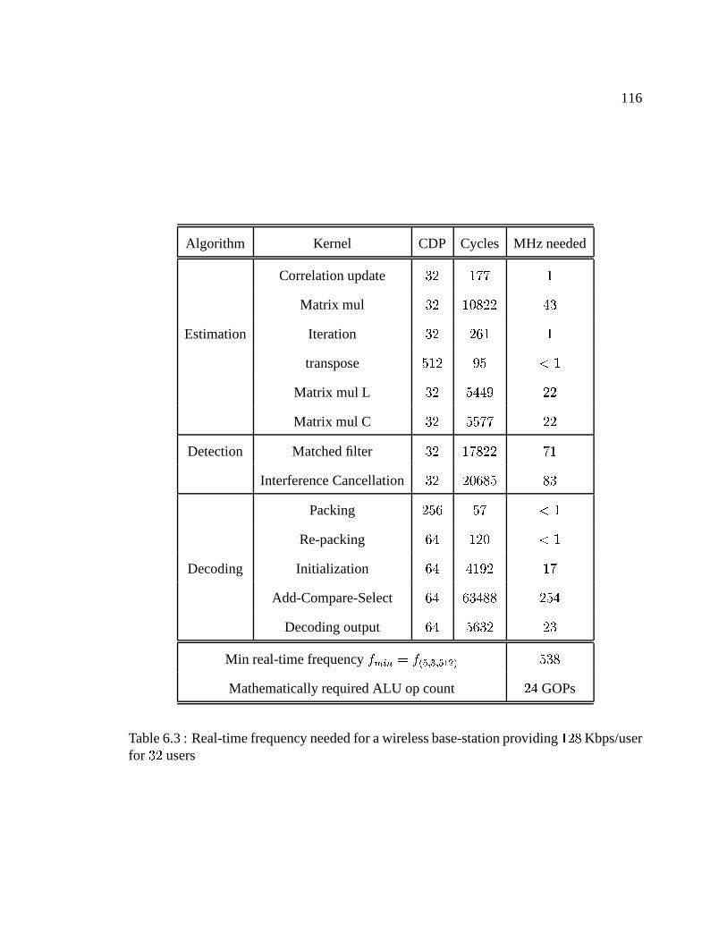
116
Algorithm Kernel CDP Cycles MHz needed
Correlation update �� ��� �Matrix mul �� ����� �
Estimation Iteration �� � � �transpose ��� �� � �
Matrix mul L �� �� ��
Matrix mul C �� ���� ��
Detection Matched filter �� ����� ��Interference Cancellation �� ���� ��
Packing �� �� � �Re-packing ��� � �
Decoding Initialization ��� ��Add-Compare-Select ��� ��
Decoding output ��� ��
Min real-time frequency�� �� � � �� �� �� ��� ���
Mathematically required ALU op count � GOPs
Table 6.3 : Real-time frequency needed for a wireless base-station providing��� Kbps/userfor �� users

117
100
101
102
103
10−3
10−2
10−1
100
Clusters
Nor
mal
ized
Pow
er
Power ∝ f2
Power ∝ f2.5
Power ∝ f3
Figure 6.5 : Minimum power point with increasing clusters and variations in� and� . Thethin lines show the variation with� . (���� ,���� ) = (5,3)
Figure 6.5 shows the variation of the normalized power with increasing clusters as clock
frequency decreases to achieve real-time execution of the workload. This is obtained from
equation (6.34). The thick lines show the ideal, no stall case of � � � and the thin lines
show the variation as� decreases to�. Figure 6.5 uses (���� ,����) = (5,3) as the number
of adders and multipliers per cluster. The figure shows that the power consumption reduces
drastically up to a factor of���� as the number of clusters reaches clusters fromclusters, since the reduction in clock frequency outweighsthe increase in capacitance due
to increased ALUs. After clusters, the increase in capacitance outweighs the small
performance benefits, increasing the power consumption. Secondly, the figure shows that
the design choice for clusters is actually independent of the value of� and� as all variations
show the same design solution.
� Cluster choice : clusters� (� , �, � )
Once the number of clusters are set, a similar exploration isdone within a cluster to
choose the number of adders and multipliers within a clusterand minimizing power using

118
1 2
3 4
5 1
2
3
400
600
800
1000
1200
(32,28)
# M
u l t i p
l i e r s
(33,34)
(39,28)
(42,37)
(36,54)
(50,31)
(43,56)
(51,42)
(64,31)
(55,62)
(65,46)
(78,18)
#Adders
(67,62)
(78,27)
(78,45)
R e
a l -
T i m
e F
r e
q u
e n
c y
( i n
M H
z )
w i t
h A
L U
u t i
l i z a
t i o
n ( +
, * ) Initial (5,3,64)
(541 MHz)
Final (3,1,64)
(567 MHz)
Figure 6.6 : Real-time frequency variation with varying adders and multipliers for� � ,� � � � �, � = 1,� � �, refining on the�� � � � �� � �� � � � � solution
equation (6.35). Figure 6.6 shows the variation of the real-time frequency with increasing
adders and multipliers. The utilization of the adders and multipliers are obtained from
a compile-time analysis using the design tool and are represented as�� � �� respectively.
The figure shows that after the (� adder,� multiplier) point there is very little benefit in
performance with more adders or multipliers. This is the point where the entire ILP is
exploited and adding more units does not produce any benefits. However, the (� adder,�multiplier) point has a higher ALU utilization for the same amount of work. Hence, one
could expect one of these configurations to be a low power solution as well. The actual low
power point depends on the variation of� � � �� in the design. For the case of� � � � �, � =
1, � � �, the �� � � � �� � �� � �� � obtains the minimum power as computed from equation
(6.35).

119
Figure 6.7 shows the power minimization sensitivity of the ALUs within each cluster
with � , � and� . The columns in Figure 6.7 represent the variations in� . The first 3 rows
show the sensitivity of the design to variations in memory stalls� , while the last row shows
the sensitivity of the design to�. By looking at the array of subplots, the following obser-
vations can be made. First, there are two candidate configurations of �� � � � �� that emerge
after a sensitivity analysis:�� � � � � and �� � �� �. Second, the design is most sensitive
to variations in� . It can be seen that� � � always selects the�� � � � � configuration and
� � � always selects the (3,1,64) configuration. This is expectedas variations in� affect the
power minimization in the exponent. Figure 6.6 shows that the �� � � � � and�� � �� � con-
figurations have among the highest ALU utilizations and thisshows the correlation between
power minimization in Figure 6.7 and ALU utilization in Figure 6.6. Third, the design is
also sensitive to memory stalls� . For � � � �� � � �, the design choice is�� � � � � and it
changes to�� � �� � as� increases. Finally, the last row shows that the design is relatively
insensitive to� variations. This is because, the register files and associated intra-cluster
communication network that get added with increase in ALUs dominate the power con-
sumption, taking�� � ��% of the cluster power for the configurations studied. The cluster
power, on the other hand, takes between�� � �% of the total chip power.
Figure 6.5 shows the cluster architecture to be lower power than the�� cluster case.
However, a cluster configuration will never attain 100% cluster efficiency as clusters
���
will remain unutilized when the CDP falls below. A cluster architecture
obtains only a�% cluster utilization for the workload but is seen to have a lower power
consumption than a�� cluster architecture with a���% cluster utilization, merely due to
the ability to lower the clock frequency, which balances outthe increase in capacitance.
Figure 6.8 shows the cluster utilization for a 32 and 64 cluster architecture. When the
CDP during execution falls below 64 (which occurs for algorithms having CDP = 32 in the

120
12
34
5
1
2
30
0.5
1
α = 0.01, β = 0, p = 2
Min = (2,1,64)
12
34
5
1
2
30
0.5
1
α = 0.01, β = 0.5, p = 2
Min = (2,1,64)
12
34
5
1
2
30
0.5
1
α = 0.01, β = 0, p = 2.5
Min = (2,1,64)
12
34
5
1
2
30
0.5
1
α = 0.01, β = 0.5, p = 2.5
Min = (3,1,64)
12
34
5
1
2
30
0.5
1
α = 0.01, β = 0, p = 3
Min = (3,1,64)
12
34
5
1
2
30
0.5
1
α = 0.01, β = 0.5, p = 3
Min = (3,1,64)
12
34
5
1
2
30
0.5
1
α = 0.01, β = 1, p = 2
Min = (2,1,64)
12
34
5
1
2
30
0.5
1
α = 0.1, β = 1, p = 2
Min = (2,1,64)
12
34
5
1
2
30
0.5
1
α = 0.01, β = 1, p = 2.5
Min = (3,1,64)
12
34
5
1
2
30
0.5
1
α = 0.1, β = 1, p = 2.5
Min = (3,1,64)
12
34
5
1
2
30
0.5
1
α = 0.01, β = 1, p = 3
Min = (3,1,64)
12
34
5
1
2
30
0.5
1
α = 0.1, β = 1, p = 3
Min = (3,1,64)
X-axis : � � � adders, Y-axis :� � � multipliers, Z-axis :� � � normalized power
Figure 6.7 : Sensitivity of power minimization to� , � and� for clusters

121
10 20 30 40 50 600
10
20
30
40
50
60
70
80
90
100
Cluster index number
Clu
ster
util
izat
ion
(%)
32 cluster architecture64 cluster architecture
Figure 6.8 : Variation of cluster utilization with cluster index
workload), clusters 33-64 remain unused for 46% of the time as there is not enough CDP
in those algorithms to utilize those clusters.
It is clear from the plot that further power savings can be obtained by dynamically
turning off entire clusters when the CDP falls below 64 clusters during execution. Since
clusters in the 64 cluster architecture consume 58% of the total power consumption of
the chip, turning off the 32 unused clusters can reduce the power consumption by up to
28% during run-time. A multiplexer network between the internal memory and clusters
can be used to provide this dynamic adaptation for power savings by turning off unused
clusters [100] using power-gating. Further power can also be saved by turning off unused
functional units when workloads having different ALU utilizations are getting executed.
The benefits due to this adaptation are limited as the ALUs consume only 25% of the
power consumption in the 64 cluster architecture configuration.
.

122
6.4.1 Verifications with detailed simulations
The design exploration tool gave two candidates as the output with variations in� , � and
� .
� Design I : �� � � � �� : �� �� �� ��
� �� � � � � ��� �� �� � � � � �� �� � �� �
� Design II : �� � � � �� : �� �� �� ��
� �� � � � � ��� �� �� � � � � �� �� � �� �
The design starts from a hypothetical infinite machine represented as�� �� �� � and
successively refines on the architecture to provide low power candidate architectures. Ta-
ble 6.4 provides the design verification of the tool (T) with acycle-accurate simulation (S)
using the Imagine stream processor simulator that can produce details on the execution
time, such as the computation time, memory stalls and microcontroller stalls. The design
tool models the compute part of the workload very realistically. The relatively small errors
are due to the assumption of ILP being independent of CDP and due to the prologue and
epilogue effects of loops in the code that were ignored. The thesis did not model� accu-
rately as it can be seen that the actual memory stalls were larger than the maximum range
used for���� ��. This is because the maximum range for
���� �� was based on the assumption
that the stalls would never exceed 25% of the execution time.This thesis observes that this
does not hold true as the execution time started to decrease with increasing clusters and
the system changed from being compute bound to memory bound.However, even after
increasing���� �� to a larger range, the design exploration tool still produces the same two
candidate choices for evaluation. Both the design candidates are also very close in their
power consumptions, with the�� � �� � configuration being only� � ��% different than
the �� � � � � configuration. An alternate graphical version of the table is shown in Figure
6.9.

123
Choice � Compute Total Real-time�
Relative Power�� � �� time Stalls time frequency �� � �� Consumption
(cycles) (cycles) (cycles) (MHz) � � � � � � �� � � �Design I T � ������ ����� ������ ���� � � � T � �� ������ ���� ���� ��
T � ������ � ������ �� �S ��� �� ���� ������ � � � � �
Design II T � �� �� ����� ����� ����� � � � T � �� �� �� ���� ������ ��
T � �� �� � �� �� ���S ���� � �� ��� � ��� � ��� � ���� ���� ����
Human T � � �� � ����� �� �� ��� � ��� T � �� � �� � ���� �� ���� ���
T � � �� � � � �� � ��S ����� ���� � ����� ���� ��� ��� � ��� ���
Table 6.4 : Verification of design tool output (T) with a detailed cycle-accurate simulation(S)
We also compare the candidate configurations from our tool with a carefully chosen
configuration [10, 100]. The analysis was done for the workload kernels based on the data
parallelism and the operation mix. A�� � � � ��� configuration was chosen since the algo-
rithms show equal number of additions and multiplications and a minimum data parallelism
of �� [10]. Our design tool provides us with lower power configurations than the carefully
chosen human configuration and improves the power efficiencyof the design by a factor of
� ��
� ��� for the chosen workload.
6.4.2 2G-3G-4G exploration
Figure 6.10 shows the real-time clock frequency for a 2G-3G-4G design exploration. The
use of the design exploration tool allows the designer to geta feel of the performance
of the system within minutes of writing the code instead of spending a lot of effort on
simulation time and deciding processor parameters, allowing the designer to quickly check

124
200
400
600
800
1000
R e
a l
- t i
m e
c l o
c k
f r e
q u
e n
c y
( M
H z )
Computations Stalls
T S T S T S Design I
(2,1,64)
Design II Human
(3,1,64) (3,3,32)
Figure 6.9 : Verification of design tool output (T) with a detailed cycle-accurate simulation(S)
the utility of the candidate algorithms in the design. The 4Gnumbers are approximate and
are based on a kernelC implementation of the code without writing the streamC code to
run the kernels. This was done since the kernels for LDPC decoding could be written and
can thus, provide performance estimates, even without the use of the streamC code, which
models the memory latency issues.
The figure shows the impact of the data rates on the real-time clock frequency require-
ments. The target data rates are used to demonstrate how an increase in data rates would
affect the real-time clock frequency without any change thealgorithms. The linear scaling
is an extrapolation since the data rates also depend on otherfactors such as bandwidth. The
reason for the extrapolation is because current systems allow support for multiple data rates
and the figure normalizes the data rates while comparing different algorithm standards. In
2G and 3G systems, Viterbi decoding had a CDP of 64 and dominated the computations.
In the 4G system, the channel estimation dominates the computation time and has a paral-

125
101
102
103
101
102
103
104
105
Data rates (Kbps)
Rea
l−tim
e cl
ock
freq
uenc
y (M
Hz)
4G*3G2G
Candidate configurations:(2,1,64) and (3,1,64) Plot based on (3,1,64)
Candidate Configurations:(1,1,32) and (2,1,32)Plot based on (2,1,32)
Figure 6.10 : Real-time clock frequency for 2G-3G-4G systems with data rates
lelism of 32. Hence, the number of clusters fell from 64 to 32 for the 4G system.
6.5 Summary
This thesis develops a design exploration tool that explores trade-offs between the orga-
nization and number of ALUs and the clock frequency in embedded stream processors.
The design methodology relates the instruction level parallelism, subword parallelism and
data parallelism to the organization of the ALUs in an embedded stream processor. The
thesis decouple the exploration phase of clusters and ALUs per cluster into independent
explorations, providing a drastic reduction in the search space. The design exploration tool
outputs candidate configurations that attain low power along with an estimate of their real-
time performance. With improvements in compilers for embedded stream processors, the
design exploration tool heuristic can also be improved by incorporating techniques such
as integer linear programming for jointly exploring�� � � � � � � � as well as exploring other

126
processor parameters such as register file sizes and pipeline depths of ALUs. Also, once
the design is done for the worst case, a multiplexer network between the internal memory
and the clusters [100] can be used to adapt the clusters in embedded stream processors
with run-time variations in the workload to further improvethe power efficiency. The next
chapter 7 shows how power efficiency in stream processors canbe improved by adapting
the compute resources to workload variations.

127
Chapter 7
Improving power efficiency in stream processors
Techniques used for high performance design and low power design are the same
– Mark Horowitz [110]
7.1 Need for reconfiguration
The design exploration scheme proposed in chapter 6 designsthe stream processor for the
worst case workload in order to ensure real-time constraints are met in the worst case.
Since real-time design constraints have to be met for the worst case, design applications
such as full capacity base-station must employ enough resources to meet those constraints
at a reasonable frequency and voltage. However, base-stations rarely operate at full ca-
pacity [111]. At lower capacity workloads, far fewer resources are required to meet the
real-time constraints, so many of the resources will be usedinefficiently.
This thesis proposes to dynamically adapt the resources of astream processor to match
the workload, improving the efficiency of stream processors. Such a adaptive stream pro-
cessor can adjust the frequency, voltage, and arithmetic resources, significantly reducing
power dissipation under lightly loaded conditions.
Stream processors exploit data parallelism available in applications and all clusters ex-
ecute the same instruction on different data sets in a SIMD manner. In order to use the
lowest voltage and frequency (power efficiency),the numberof clusters used in a stream
processor should be designed depending on the data parallelism available in the applica-

128
tion. Table 7.1 shows the available data parallelism� for the base-station with variation in
the number of users (U) and the decoding constraint length (K). While it is possible to vary
other system parameters such as the coding rate (R) and the spreading gain (N) in the table,
we decided to keep them constant in order to fix the target datarate to 128 Kbps/user as
changing these two parameters affects the target data rate as well in wireless standards [14].
From the table, we can observe that the available data parallelism reduces as we go from
the full capacity base-station case of 32 users, constraintlength 9 (32,9) to lower capacity
systems. Based on the data parallelism, if we choose a 32-cluster architecture as the worst
case architecture for evaluation, we see that as we go down from case (32,9) to other cases,
none of the other workloads meet the minimum data parallelism required to keep all the
clusters busy. Hence, there needs to be reconfiguration support provided in stream proces-
sors to turn off unused clusters and allow clusters to dynamically match the available data
parallelism in the workload.
7.2 Methods of reconfiguration
Three different mechanisms could be used to reroute the stream data appropriately: by
using the memory system, by using conditional streams, and by using adaptive stream
buffers.
7.2.1 Reconfiguration in memory
A data stream can be realigned to match the number of active clusters by first transferring
the stream from the SRF to external memory, and then reloading the stream so that it only is
placed in SRF banks that correspond to active clusters. Figure 7.1 shows how this would be
�The data parallelism in this context is defined as the data parallelism available after packing and loop
unrolling

129
Workload Estimation Detection Decoding
(U,K)�(U,N)
�(U,N)
�(U,K,R)
(4,7) 32 4 16
(4,9) 32 4 64
(8,7) 32 8 16
(8,9) 32 8 64
(16,7) 32 16 16
(16,9) 32 16 64
(32,7) 32 32 16
(32,9) 32 32 64
Table 7.1 : Available Data Parallelism in Wireless Communication Workloads ( U = Users,K = constraint length, N = spreading gain (fixed at 32), R = coding rate(fixed at rate 1/2)).The numbers in columns 2-4 represent the amount of data parallelism
accomplished on an eight cluster stream processor. In the figure, a 16 element data stream,
labeled Stream A in the figure, is produced by a kernel runningon all eight clusters. For
clarity, the banks within the SRF are shown explicitly and the stream buffers are omitted.
Therefore, the stream is striped across all eight banks of the SRF. If the machine is then
reconfigured to only have four active clusters, the stream needs to be striped across only the
first four banks of the SRF. By first performing a stream store instruction, the stream can
be stored contiguously in memory, as shown in the figure. Then, a stream load instruction
can be used to transfer the stream back into the SRF, only using the first four banks. The
figure shows Stream A as the result of this load. As can be seen in the figure, the second
set of four banks of the SRF would not contain any valid data for Stream A .
This mechanism for reconfiguration suffers from several limitations. First, the memory

130
SRF
Stream A
0 1 2 3 4 5 6 7 8 9 10 11 12 13 14 15
0 8
7 15
6 14
5 13
4 12
3 11
2 10
1 9
0 4 8 12
1 5 9 13
2 6 10 14
4 7 11 15
X X X X
To
Cluster 0
To
Cluster 7
To
Cluster 6
To
Cluster 5
To
Cluster 4
To
Cluster 3
To
Cluster 2
To
Cluster 1
Stream A'
Step 1: Store
stream A to memory Step 2: Load into
stream A'
Figure 7.1 : Reorganizing Streams in Memory
access stride needed to transfer the data from 8 clusters to 4clusters is not regular. The
non-uniform access stride makes the data reorganization anextremely difficult task and in-
creases memory stalls. Next, the reconfiguration causes memory bank conflicts during the
transfer as multiple reads (during reconfiguration to higher number of clusters) or writes
(during reconfiguration to lower number of clusters) are needed from the same bank. Also,
one of the motivations for stream processor design is to keepthe arithmetic units busy so
that data transfer between memory and the processor core is minimized. Forcing all data
to go through memory whenever the number of active clusters is changed directly violates
this premise. In Chapter 5, we show that using external memory to reorganize data streams
for Viterbi decoding results in a larger execution time thanif the reorganization were done
within the clusters. Finally, memory operations are expensive in terms of power consump-

131
Conditional Buffer Data
Condition Switch
Data received
0
A
1
A
B
1
B
C
0
-
D
0
-
1 2 3 Cluster index 0
1
C
1
D
C
0
-
D
0
-
1 2 3
A B
Access 0 Access 1
A 4-cluster stream processor reconfiguring to 2
clusters using conditional streams
Figure 7.2 : Reorganizing Streams with Conditional Streams
tion. The increase in power consumption combined with the increase in execution time due
to stalls makes reconfiguration using memory an undesirablesolution for reconfiguration.
7.2.2 Reconfiguration using conditional streams
Stream processors already contain a mechanism for reorganizing data streams using condi-
tional streams [112]. Conditional streams allow data streams to be compressed or expanded
in the clusters so that the direct mapping between SRF banks and clusters can be violated.
When using conditional streams, stream input and output operations are predicated in each
cluster. If the predicate is true (1) in a particular clusterthen it will receive the next stream
element, and if the predicate is false (0), it will receive garbage. As an example, consider
an eight cluster stream processor executing a kernel that isreading a stream conditionally.
If clusters 1, 5, and 7 have a true predicate and the other clusters have a false predicate,
then cluster 1 will receive the first stream element, cluster5 will receive the second stream
element, and cluster 7 will receive the third stream element. The first cluster to have a

132
true predicate on the next read operation will receive the fourth stream element. In this
way, conditional input streams are delivered to the clusters in a sparse manner. Similarly,
conditional output streams compress data from disjoint clusters into a contiguous stream.
In order to use conditional streams to deactivate clusters,the active clusters would al-
ways use a true predicate on conditional input or output stream operations and inactive
clusters would always use a false predicate. This has the effect of sending consecutive
stream elements only to the active clusters. As explained in[112], conditional streams are
used for three main purposes: switching, combining, and load balancing. Using condi-
tional streams to completely deactivate a set of clusters isreally a fourth use of conditional
streams.
In a stream processor, conditional input streams are implemented by having each cluster
read data from the stream buffer as normal, but instead of directly using that data, it is first
buffered. Then, based upon the predicates, the buffered data is sent to the appropriate
clusters using an intercluster switch [112]. Conditional output streams are implemented
similarly: data is buffered, compressed, and then transferred to the SRF. Therefore, when
using conditional streams, inactive clusters are not trulyinactive. They must still buffer and
communicate data. Furthermore, if conditional streams arealready being used to switch,
combine, or load balance data, then the predicates must be modified to also account for
active and inactive clusters, which complicates programming.
7.2.3 Reconfiguration using adaptive stream buffers
From Figure 4.2, we can observe that the input to the clustersarrive directly from the stream
buffers, which are banked to match the number of clusters. Thus, if the data parallelism
decreases below the number of clusters, the data for the stream will lie in the wrong bank
and hence, cannot be accessed directly by the correspondingcluster.

133
Therefore, to successful deactivate clusters in a stream processor, stream data must be
rerouted so that active clusters receive the appropriate data from other SRF banks as well.
Hence, an interconnection network between the stream buffers and the clusters is needed
in order to adapt the clusters to the data parallelism. A fully connected network allowing
data to go to any cluster would be extremely expensive in terms of area, power and latency.
In fact, stream processors already have a inter-cluster communication network that can be
used to route data to any cluster. The intercluster communication network is not only a
significant part of cluster power dissipation, but have large latency and area requirements
as well.
To investigate better networks, we make use of the fact that it is not necessary to ar-
bitrarily turn off any cluster since all clusters are identical. Hence, we only turn off only
those clusters whose cluster identification number is greater than the data parallelism in
the algorithms. We further simplify the interconnection network by making the clusters
turn off only in powers of two, since most parallel algorithmworkloads generally work on
datasets in powers of two.
The reconfigurable stream processor is shown in Figure 7.3. The reconfigurable stream
processor allows the ability to turn the clusters on and off,depending on the available data
parallelism using an interconnection network within the stream buffers. This interconnec-
tion network allows the stream buffers to become adaptive tothe workload. In the absence
of any reconfiguration needed such as in case (32,9) of Table 7.1, the interconnection net-
work acts as an extended stream buffer, providing the ability to prefetch more data while
behaving as a reconfiguration support when the data parallelism reduces below the number
of clusters.
Figure 7.3 shows how the adaptive stream buffers would operate if reconfiguration is
needed. The switches in the mux/demux network are set to control the flow of the data to

134
the clusters. There are���
� �� � stages required in the stream buffer if complete reconfigu-
ration to a single cluster is desired, where�
is the number of clusters. The reconfiguration
network allows the stream processor to stripe and access data across all the SRF banks and
provides high memory efficiency as well instead of limiting the data storage to that of the
parallelism present in the data stream and zero-padding unused SRF banks. The adaptive
stream buffers also provide higher SRF bandwidth to applications with insufficient data par-
allelism since all the SRF banks can be accessed and utilizedeven in cases with insufficient
data parallelism.
The example in Table 7.2 shows a 4-cluster stream processor reconfiguring to 1 cluster.
We can see that each stage of the multiplexer network holds the data until it is completely
read into the clusters. This is done using counters for each stream buffer stage (not shown
for clarity). Also, stalls need to be handled by the multiplexer network. The adaptive
stream buffer network adds a latency of���
� �� � to the data entering the clusters. However,
the adaptive stream buffers can prefetch data even if the clusters are stalled, allowing it to
have the potential to hide latencies or even improve performance if clusters have significant
stalls.
The multiplexer/demultiplexer network shown in Figure 7.3is per data stream. Each
input stream is configured as a multiplexer and each output stream is configured as a de-
multiplexer during execution of a kernel. The cluster reconfiguration is done dynamically
by providing support in the instruction set of the host processor for setting the number of
active clusters during the execution of a kernel. By default, all the clusters are turned off
when kernels are inactive, thereby providing power savingsduring memory stalls and sys-
tem initialization. Another advantage of providing reconfiguration using the multiplexer
network is that users do not have to modify their kernel code to account for this reconfigu-
ration support.

135
SB
C
SB
C
SB
C
SB
C
SB
C
SB
C
SB
C
SB
C
SB
C
SB
C
SB
C
SB
C
(a) Reconfiguring to 4 clusters
( b ) Reconfiguring to 2 clusters
( c ) Reconfiguring to 1 cluster
Stage 1
Stage 2
Clusters
Figure 7.3 : Reorganizing streams with an adaptive stream buffer
The current implementation of the multiplexer network addsa latency of���
� �� � � �
cycle for the data to flow through the multiplexer network. Hence, all the data entering the
clusters are delayed by 7 cycles for a 32-cluster stream processor. However, the multiplexer
network behaves as an extended stream buffer and allows dataprefetching to occur in the
multiplexer network, allowing the ability to absorb the latency. Also, it is possible that the
kernel does not read the data during the first 7 cycles (or the kernel can be re-scheduled by
the compiler such that the first read occurs after 7 cycles). However, the current implemen-
tation stalls the clusters for 7 cycles for all kernels. In spite of this, we can see a reduction
in the micro-controller stalls for some of the kernels. Table 7.3 compares the reconfig-
urable stream processor with the base stream processor for the full capacity base-station
case (32,9) that does not require any reconfiguration, thereby allowing us to evaluate the
worst case performance of the dynamically reconfigurable processor. From the table, we
can observe that for kernels such as ’matrix multiplicationfor L’, there was a reduction in

136
Input Data from SB :ABCDEFGH
Time Stage 1 Stage 2 Cluster
1 ABCD - -
2 ABCD AB -
3 ABCD AB A
4 ABCD CD B
5 EFGH CD C
6 EFGH EF D
7 EFGH EF E
: : : :
Table 7.2 : Example for 4:1 reconfiguration case (c) of Figure7.3. Y-axis represents time.Data enters cluster 1 sequentially after an additional latency of 2 cycles
the stall time due to the adaptive stream buffers, although the net result was a slight degra-
dation in performance. The current implementation for the reconfigurable stream processor
needs to run at 1.12 GHz to meet real-time constraints as opposed to 1.03 GHz for a tra-
ditional stream processor when no reconfiguration is required. However, by turning off
the clusters when memory stalls are present, the reconfigurable stream processors can still
more power-efficient even in the no reconfiguration case, andthis is is shown in the next
section.
7.3 Imagine simulator modifications
A ’setClusters(int clusters)’ is added in the stream code to set the number of clusters re-
quired for the kernel execution. This instruction is scheduled to execute just before the

137
Kernel Calls Base New
busy stalls busy stalls
Update channel matrix 1 223 544 223 533
Matrix multiplication 1 12104 4934 11464 5324
Iterate for new estimates 1 272 996 206 1057
Matrix mult. for L 1 6537 67 6218 22
Matrix mult. for C 1 6826 2075 6506 2052
Matrix transpose 5 1075 1425 1070 1380
Matched Filter 67 18492 2479 18492 3752
Interference Cancellation 197 35854 13396 35854 17139
Pack data 1 289 0 289 7
Repack data 6 444 24 444 54
Viterbi Init. 32 4736 0 4736 224
Add Compare Select 1024 114688 0 114688 7168
Extract Decoded bits 32 5952 0 5792 224
Kernel Time 223432 25940 224918 38936
Memory Time - 25261 - 34645
Total Time 258693 298499
Real-time frequency 1.03 GHz 1.2 GHz
Table 7.3 : Worst case reconfigurable stream processor performance

138
kernel executes and gets reset at the end of the kernel to zeroso that the clusters can be
turned off for the maximum time period possible. The streamCcode now looks as follows:
:
setClusters(16); //use 16 clusters only for the next kernel
kernel1(input1,input2,input3,.. , output1);
setClusters(8);
kernel2(input1,....,output1, output2,...);
:
7.3.1 Impact of power gating and voltage scaling
Power gating and voltage scaling are recent innovations in providing power-efficiency in
microprocessors. Their impact on reconfiguration is presented in this thesis.
Power gating [105, 113, 114] gates the supply voltage to the functional units. The main
advantage of power gating is to save leakage power, which is becoming increasingly impor-
tant in processor design due to technology scaling. The gated circuitry does not dissipate
any power when turned off. However, there is power dissipation by the gating circuitry
and the power switching device itself. Figure 7.4 shows an example of the power gating
functionality. The power switching device needs to be largeenough in width to handle
the average supply current during operation. Note that for turning off clusters using power
gating, the width required would exceed maximum transistorwidths. This is because, the
clusters consume�80% of the chip power. Hence, in this case, multiple power gating
devices need to be used to turn off a single cluster.
The addition of a gating device can result in reduced performance and decreased noise
margins due to the drop across the gating device and the parasitic capacitances added.

139
Functional
Unit
V dd
GND
TurnOffALU
Figure 7.4 : Power gating
Also, there is a latency between the arrival of the signal to turn on the functional unit and
the operation of the functional unit. Due to huge capacitances on the power supply nodes,
several clock cycles will be needed to allow the power supplyto reach its operating level.
Dynamic voltage scaling (DVS) allows the scaling of the processor voltage and clock
frequency, depending on the application’s requirements. Processors generally operate at a
fixed voltage and require a regulator to control the voltage supply variation. The voltage
regulator for DVS is different from a standard voltage regulator [115]. This is because
in addition to regulating voltage for a given frequency, it must also change the operating
voltage, when a new frequency is requested. Since the hardware has no knowledge of the
time for voltage and frequency switching, the operating system software controls the clock
frequency by writing to a register in the system control state.
7.4 Power model
Don’t believe the 33rd order consequences of a first order model
– Golomb’s Don’ts of mathematical modeling
The power model for stream processors is based on [23] with additions to account for
the adaptive stream buffers. The parameters used in power analysis in this thesis are as
shown in Table 7.4 and Table 7.5. All energy values shown are with respect to�� . Based

140
Description Value
ALU operation energy 632578
LRF access energy 79365
Energy of SB access/bit 155
SRAM access energy/bit 8.7
SP access energy 1603319
Norm. wire energy/track(�� ) 1
Table 7.4 : Power consumption table (normalized to�� units)
on the models in [23], with modifications to account for fixed point ALUs, the length of
a wire track is� �� micron, a cluster is 1400 wire tracks wide and it takes� � pJ to
propagate a signal across a single wire track. The modifications are based on a low power
version of stream processors for embedded systems (See (LP)in Chapter 6 in [116]). The
power consumption of the mux network is wire length capacitance dominant to a first order
approximation [23]. Assuming a linear layout of the clusters (worst case), the total wire
length of the mux network for� bit is � � units, where the unit is the distance between
� clusters. For 8 streams with 32 bits of wire each, the mux network uses a total wire of
length approximately� � � ��� � � � �� � � �� � �� meters with a power consumption of
5 �J [23]. An on-off latency of 7 cycles is based on clocking the multiplexer network. The
pipelining depth of the multiplexer network���
� �� ������ ��. For a 32-cluster architecture,
this evaluates to 5 cycles. In addition, 2 cycles are added during interfacing the network to
the SRF and the clusters.
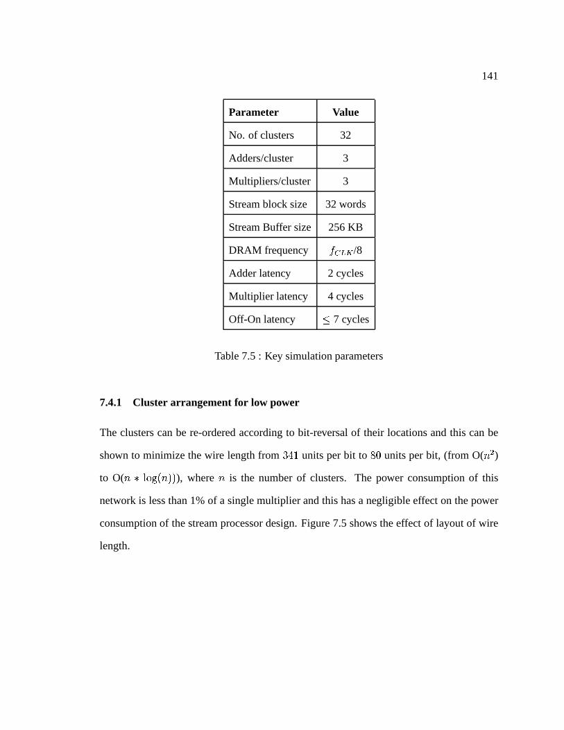
141
Parameter Value
No. of clusters 32
Adders/cluster 3
Multipliers/cluster 3
Stream block size 32 words
Stream Buffer size 256 KB
DRAM frequency�� /8
Adder latency 2 cycles
Multiplier latency 4 cycles
Off-On latency � 7 cycles
Table 7.5 : Key simulation parameters
7.4.1 Cluster arrangement for low power
The clusters can be re-ordered according to bit-reversal oftheir locations and this can be
shown to minimize the wire length from� � units per bit to�� units per bit, (from O(��)to O(� � ��� �� ��), where� is the number of clusters. The power consumption of this
network is less than 1% of a single multiplier and this has a negligible effect on the power
consumption of the stream processor design. Figure 7.5 shows the effect of layout of wire
length.

142
S
C
S
C
S
C
S
C
(a) Original layout
S
C
S
C
S
C
(b) Modified layout to
minimize inter-connection
lengths
S
C
0 1 2 3 2 0 1 3
Figure 7.5 : Effect of layout on wire length
7.5 Results
7.5.1 Comparisons between reconfiguration methods
There have been three different methods of reconfiguration proposed in this chapter, namely
(a) Reconfiguration in memory, (b) Reconfiguration using conditional streams and (c) Re-
configuration using a multiplexer network.
Out of the three, only (a) and (c) allow the processor to completely turn off the unused
clusters. This is because (b) requires the use of the scratchpad and the inter-cluster com-

143
munication network in order to support conditional streams. The ALUs in (b) can still be
turned off to save power. However, the scratchpad and the inter-cluster network are two of
the most expensive parts in the clusters in terms of power consumption [23], and hence, the
ability for power savings using (b) for reconfiguration is limited.
Reconfiguration in memory suffers from numerous disadvantages. First, it requires a
special stride pattern that is not native to the stream processor. For example, when a 4-
cluster processor reconfigures to 2-clusters using memory,the stride pattern is [1 2 5 6 ....],
which is a specialized stride access pattern and would require explicit hardware and soft-
ware support to maintain for reconfiguration. Secondly, moving data via memory adds a
significant latency to the reconfiguration. For example, chapter 5 shows that moving data
via clusters is more than a order-of-magnitude faster than moving data via memory for op-
erations such as a matrix transpose which has a strided memory access pattern. Finally, it
increases the memory requirements of the processor. For example, while reconfiguration
to half the number of clusters, a matrix of size� �� requiring� rows in a� -cluster ma-
chine, will require�� rows after reconfiguration to��� clusters. Hence, reconfiguration
in memory is not considered as a viable solution for adaptingthe data parallelism.
Hence, it can be seen that reconfiguring using the multiplexer network is the only so-
lution that allows power savings with a minimum impact on theexecution time. Figure
7.6 quantifies the amount of execution time increase due to the introduction of the multi-
plexer network. In order to compare the increase in execution time, a 32-user system with
constraint length 9 Viterbi decoding is considered. This system does not require any re-
configuration. Hence, Figure 7.6 allows us to see the overhead of providing the ability to
reconfigure using conditional streams (CS) and the overheadof providing reconfiguration
using a multiplexer network (MUX) between the SRF and the clusters. It can be seen that
the multiplexer network has a lower latency than conditional streams but is more expensive

144
Base CS MUX0
0.5
1
1.5
2
2.5
3
3.5x 10
5
Reconfiguration methods
Exe
cutio
n T
ime
(cyc
les)
(32,9) on 32−clusters using Base, Conditional Streams (CS), Mux Network (MUX)
ComputationsStalls
Figure 7.6 : Comparing execution time of reconfiguration methods with the base processorarchitecture
if there is no reconfiguration in the system (Base).
Figure 7.7 shows the impact of the conditional stream reconfiguration (CS) and the
multiplexer network reconfiguration (MUX) as the constraint length in the system changes
from constraint length 9 to constraint length 7 on 32-clusters. Thus, it can be seen that
reconfiguration using the multiplexer network not only permits the ability to turn off clus-
ters for power savings but also provides a faster execution time than reconfiguration using
conditional streams.
7.5.2 Voltage-Frequency Scaling
Figure 7.8 shows the clock frequency needed by the reconfigurable stream processor to
meet real-time requirements of 128 Kbps/user. We can see that as the workload decreases,
the percentage of cluster busy time and microcontroller stalls decrease. However, the mem-

145
CS MUX0
0.5
1
1.5
2
2.5
3x 10
5
Reconfiguration methods
Exe
cutio
n T
ime
(cyc
les)
Re−configuring to (32,7) on 32−clusters using Conditional Streams (CS), Mux Network (MUX)
ComputationsStalls
Figure 7.7 : Impact of conditional streams and multiplexer network on execution time
ory stall time does not decrease with the workload. This is because as the workload de-
creases from (32,9) to the (4,7) case, some of the memory stalls that were hidden during
kernel execution suddenly became visible due to the corresponding decrease in the kernel
execution time. The reconfigurable stream processor needs to run at 1.12 GHz to meet real-
time for the full capacity workload and can run at 345.1 MHz when the workload decreases
to the (4,7) case.
Figure 7.9 shows the corresponding cluster utilization variation with the workload and
the cluster index. We can see that in the full capacity case (32,9), all clusters are equally
utilized at 87%. The clusters are idle and are turned off 13% of the time due to memory
stalls. However, as the workload decreases, the reconfigurable stream processor turns off
unutilized clusters to lower their utilization factor and save power. For example, we can
see in case (4,9) that only the first 4 clusters are being used at 63% utilization, while the re-
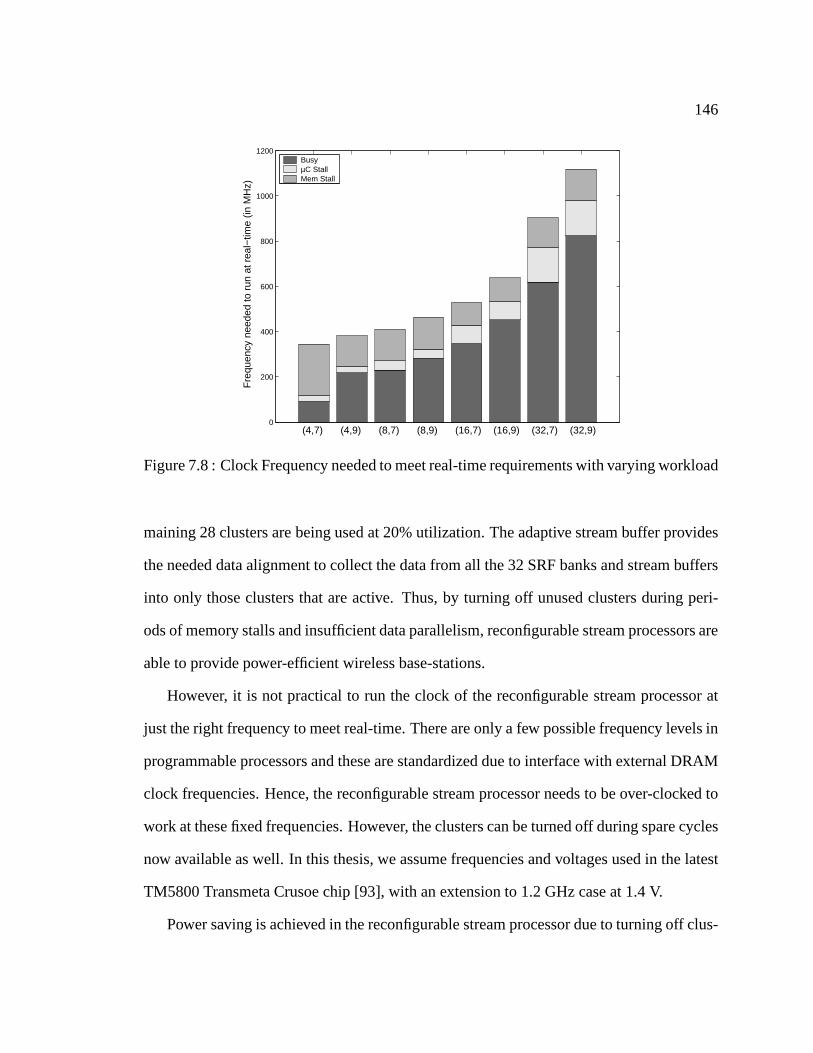
146
0
200
400
600
800
1000
1200
Fre
quen
cy n
eede
d to
run
at r
eal−
time
(in M
Hz)
(4,7) (4,9) (8,7) (8,9) (16,7) (16,9) (32,7) (32,9)
BusyµC StallMem Stall
Figure 7.8 : Clock Frequency needed to meet real-time requirements with varying workload
maining 28 clusters are being used at 20% utilization. The adaptive stream buffer provides
the needed data alignment to collect the data from all the 32 SRF banks and stream buffers
into only those clusters that are active. Thus, by turning off unused clusters during peri-
ods of memory stalls and insufficient data parallelism, reconfigurable stream processors are
able to provide power-efficient wireless base-stations.
However, it is not practical to run the clock of the reconfigurable stream processor at
just the right frequency to meet real-time. There are only a few possible frequency levels in
programmable processors and these are standardized due to interface with external DRAM
clock frequencies. Hence, the reconfigurable stream processor needs to be over-clocked to
work at these fixed frequencies. However, the clusters can beturned off during spare cycles
now available as well. In this thesis, we assume frequenciesand voltages used in the latest
TM5800 Transmeta Crusoe chip [93], with an extension to 1.2 GHz case at 1.4 V.
Power saving is achieved in the reconfigurable stream processor due to turning off clus-

147
0 5 10 15 20 25 30 0
50
100
(4,9)
(4,7)
0 5 10 15 20 25 30 0
50
100 (8,9)
(8,7)
0 5 10 15 20 25 30 0
50
100
(16,9)
(16,7)
0 5 10 15 20 25 30 0
50
100
(32,9)
(32,7)
Cluster index
C l u
s t e
r U
t i l i z a
t i o
n (
% )
Figure 7.9 : Cluster utilization variation with cluster index and with workload
ters during over-clocking (the idle time due to mismatch between the frequency needed and
the actual frequency used), during memory stalls and duringkernels having clusters with
insufficient data parallelism. This is shown in Table 7.6. Inorder to evaluate the benefits
of the adaptive stream buffers, the base case comparison is assumed to be a stream pro-
cessor that already supports dynamic voltage and frequencyscaling. We can see from the
table that the adaptive stream buffers yields savings in power even in the no reconfigura-
tion case (32,9) of a full capacity base-station due to turning off clusters during memory
stalls and over-clocking. We can see that the adaptive stream buffers yield an additional
15-85% power savings over that provided by simple frequencyand voltage scaling in the
architecture.

148
Workload Freq (MHz) Voltage Power Savings (W) Power (W) Savings
needed used (V) clocking Memory Clusters New Base
(4,7) 345.09 433 0.875 0.325 1.05 0.366 0.30 2.05 85.14 %
(4,9) 380.69 433 0.875 0.193 0.56 0.604 0.69 2.05 66.41 %
(8,7) 408.89 433 0.875 0.089 0.54 0.649 0.77 2.05 62.44 %
(8,9) 463.29 533 0.950 0.304 0.71 0.643 1.33 2.98 55.46 %
(16,7) 528.41 533 0.950 0.020 0.44 0.808 1.71 2.98 42.54 %
(16,9) 637.21 667 1.050 0.156 0.58 0.603 3.21 4.55 29.46 %
(32,7) 902.89 1000 1.300 0.792 1.18 1.375 7.11 10.46 32.03 %
(32,9) 1118.25 1200 1.400 0.774 1.41 0.000 12.38 14.56 14.98 %
Estimated Cluster Power Consumption 78 %
Estimated SRF Power Consumption 11.5 %
Estimated Microcontroller Power Consumption 10.5 %
Estimated Chip Area 45.7�� �
Table 7.6 : Power Savings

149
7.5.3 Comparing DSP power numbers
A 3G base-station built in software requires� 24 GOPs (theoretical arithmetic operations).
This exceeds the current capabilities of single processor DSP systems. It becomes very
difficult to compare multi-processor DSP systems due to variations in processor technol-
ogy, area, target performance, clock frequency, memory andfunctional units. This thesis
makes an attempt to provide estimates of how a stream processor benefits over a system
design where multiple DSPs are connected together. Typicalnumbers quoted for DSPs
requiring the implementation of sophisticated algorithmshave been 1 DSP per user [117].
A 3G base-station design in software may require 32 DSPs at 600 MHz to meet perfor-
mance requirements, when including memory stalls, compiler efficiencies and algorithmic
dependencies. Hence, a 32 DSP architecture at 600 MHz may be useful to compare and
contrast power consumptions for the physical layer processing in wireless base-stations. [A
600 MHz TI VLIW DSP was chosen as the reference DSP as comparison numbers were
available for the DSP for that frequency [118] and for the same process technology as the
Imagine stream processor implementation].
Table 7.5.3 shows the power consumption of 32 C64x DSPs, withpower numbers for
a 600 MHz C64x DSP at 1.2 V, implemented in a 0.13�m process technology taken
from [118]. It can be seen that 32 C64x DSPs consume 35.2 W of power when includ-
ing I/O and EMIF peripherals. However, if the peripherals are excluded, 32 DSP cores
consume 10.22 W of power. In contrast, a 32-cluster stream processor with 4 16x16 mul-
tipliers in each DSP (to make a fair comparison with the TI DSP) consumes 9.6 W of
power at 600 MHz. This is because there is only a single micro-controller in the stream
processor that issues instructions to all units compared to32 micro-controllers in the 64x
DSP cores. However, note that these numbers are to be taken only as a rough estimate of
power consumption due to variations in process technology and design parameters such as

150
Processor Power
1 C64x DSP core (CPU + L1) 0.31 W
1 C64x DSP core (CPU + L1 + L2 + EMIF) 0.72 W
1 C64x DSP chip (total) 1.1 W
32 C64x DSP chips � 35.2 W
32 C64x DSP cores (CPU + L1) � 10.22 W
32 cluster stream processor 9.6 W
Table 7.7 : Comparing DSP power numbers. The table shows the power reduction asthe extraneous parts in a multi-processor DSP are eliminated to form a single chip streamprocessor
the number of registers and as the actual power consumption can be determined only by an
implementation. The inter-cluster communication networkbetween the DSPs is accounted
for in the stream processor while an ideal inter-cluster communication network is assumed
for the TI DSPs. Hence, the power consumption of 32 C64x DSP cores will actually be
greater than 10.22 W.
7.5.4 Comparisons with ASIC based solutions
Figure 7.10 shows the performance comparisons between DSPs, stream processors and
ASICs for Viterbi decoding. The reason for using Viterbi decoding as a comparison point is
that Viterbi decoding being a well-known and implemented algorithm can be used for pre-
dicting the performance of stream processors against ASIC implementations. The Viterbi
decoding algorithm can be easily implemented on ASICs and FPGAs to meet 1 bit per
clock cycle, requiring 128 KHz to provide 128 Kbps data rate,assuming a fully unrolled
system [119]. The DSP and the stream processor numbers have been obtained from a

151
software implementation.
It is interesting to see from the figure that both stream processors and ASICs show the
same characteristics while exploiting data-parallelism in the ACS computations. The figure
assumes that the ASIC is able to decode� � �� �� bits every clock cycle. The effective DP
for a constraint length K decoder is���
. However, the stream processor implementation
exploits subword parallelism and does 4 ACS operations in 1 cluster. Hence, to make the
plot scale the same, 4 ACS units in the ASIC are grouped together as a single ACS unit,
giving rise to a net maximum DP on the graph as� ��. Typical Viterbi decoders [119, 120]
are able to decode a bit every clock cycle. Hence, it is assumed that with lower number
of ACS units, they would scale linearly in frequency, especially since the clock frequency
range is in KHz. There is a 2 orders-of-magnitude performance difference between the
stream processor implementation and an ASIC/FPGA implementation while there is a 1-2
order-of-magnitude difference between the stream processor implementation and a single
processor C6416 DSP implementation. The single dot in the figure refers to a software
DSP implementation of Viterbi decoding for constraint length 9. This difference translates
to power as well. For example, if an ASIC were to run at 128 KHz,it’s power consumption
would translate roughly to around 100�W extrapolating from numbers in [119, 120] com-
pared to a 100 mW stream processor implementation at around 10 MHz. In contrast, the
C64x DSP would take around 250 mW for a full software implementation at around 400
MHz. A C64x DSP with a co-processor solution would perform similar to the ASIC solu-
tion with an additional overhead of the data transfer between the DSP and the co-processor.
However, the overhead of such data transfer is typically less than 5% and does not impact
the order-of-magnitude differences in comparisons. The ASIC and stream processor num-
bers for power should only be taken as rough estimates as hardware implementations are
needed for accurate comparisons.

152
100
101
102
10−1
100
101
102
103
Data Parallelism (Number of clusters)
Fre
quen
cy n
eede
d to
atta
in r
eal−
time
(in M
Hz)
Viterbi decoding for rate 1/2 for 1 user at 128 Kbps each user
K = 9K = 7K = 5
Stream Processor
ASIC decoding DP/2K−3 bits every clock cycle
TI C64x DSP (w/o co−processors)
Figure 7.10 : Performance comparisons of Viterbi decoding on DSPs, stream processorsand ASICs
7.6 Summary
This chapter shows how power efficiency in stream processorsdesigned for the worst case
in chapter 6 can be improved by using an adaptive multiplexernetwork that adapts the
compute resources in the design to the workload variations.There are different ways of
reconfiguring the data to use the right number of clusters. However, only the multiplexer
network allows the stream processor to turn off unused clusters thereby adapting the clus-
ters to the data parallelism of the application. Dynamic voltage and frequency scaling adapt
the voltage and frequency to match the real-time requirements. Thus, by adapting clusters
and the frequency in the stream processor, power efficiency of the DSP is improved, pro-
viding significant savings in power while maintaining real-time performance.

153
Chapter 8
Conclusions and Future Work
8.1 Conclusions
Traditional DSP architectures have explored (ILP, SubP) parallelism space for providing
high performance DSP architectures. Data-parallel DSPs have taken the traditional DSP
architecture space a step further to (ILP, SubP, DP) by exploiting the explicit data paral-
lelism in signal processing applications. This thesis usesstream processors as reference
data-parallel DSP for evaluating the contributions of thisthesis. This thesis explores the
processor architecture space and provides power efficiencyand efficient algorithm mapping
for stream processors.
This thesis addresses the design of stream processors for high performance real-time
embedded applications. This thesis first shows the design ofalgorithms for efficient map-
ping on stream processors such that they provide execution time benefits while simultane-
ously simplifying the DSP architecture by demonstrating patterns in the inter-cluster com-
munication network. The thesis then takes the next step of designing the stream processor
and setting the number of arithmetic units, clusters and theclock frequency such that the
stream processor meets real-time requirements with the minimum power consumption. Fi-
nally, the thesis improves power efficiency in stream processors designed using the above
exploration by adapting the compute resources to run-time variations in the workload.
The increase in the parallelism space for stream processorscomes at an associated cost
of increase in complexity of the tools that are needed to utilize the architecture efficiently.

154
At the time of this thesis, there are still no compilers that can take code written in standard
programming languages such as C and run them efficiently on the stream processors dis-
cussed in this thesis. Although the availability of highly data parallel applications allows
significant performance benefits for stream processors, there are performance limits in this
(ILP, SubP, DP) space as well. If the applications need for performance is greater than
the available (ILP, SubP, DP), other parallelism levels such as thread-level parallelism or
pipelining multiple DSPs can be considered. This, of course, comes at a cost of increased
complexity of the design tools.
8.2 Future work
8.2.1 MAC layer integration on the host processor
This thesis focuses on the compute parts of the algorithms indata-parallel high perfor-
mance DSP applications. In most cases, these applications interface with other layers in
the system. For example, a wireless system after processingthe data in the physical layer,
needs to interface the data output with other layers such as the MAC layer. The control
aspects of the MAC and higher layers could create potential bottlenecks in the system.
8.2.2 Power analysis
Don’t believe that the model is the reality
– Golomb’s Don’ts of mathematical modeling
The power model used in this thesis is an extrapolated model based on the base stream
processor implementation for the Imagine architecture at Stanford. Although the thesis has
done a sensitivity analysis of the design to the power model,the use of voltage-frequency
scaling, power gating and cluster variations can cause errors in the design and power esti-

155
mates, especially when mapped to newer technology processes such as 90 nm technology
processes. A hardware implementation is needed in order to verify the performance and
power benefits that are shown to be achievable in this thesis.
8.2.3 Pipelined, Multi-threaded and reconfigurable processors
Pipelining and multi-threading are ways to increase the performance beyond that obtained
by data parallelism. However, tools need to be designed thatautomate partitioning of
data on multiple pipelined resources and provide dynamic load balancing. Multi-threading
designs need to ensure that real-time constraints are not violated due to multi-threading
as the threading analysis is usually dynamic. Reconfigurable computing are new concepts
for designing DSP applications. The architectures and tools were not stabilized during this
thesis investigation. Reconfigurable computing shows considerable promise for the DSP
domain, if tools can be designed for efficient mapping algorithms written in high level
languages on such processors.
8.2.4 LDPC and Turbo decoding
As explained in Chapter 5, the data access pattern for LDPC decoding requires the use of
an indexed SRF [92]. Implementing LDPC decoding would require considerable change in
the simulator tools and changes in the thesis made using the tools would have to be ported
to the new simulator tools. Hence, it has been left as future work at this point in time.
However, the use of the indexed SRF makes the LDPC decoding implementation similar to
Viterbi decoding and this has been studied in depth in Chapter 5. The use of indexed SRF
would also assist in building random interleavers needed for Turbo decoding, as discussed
in Chapter 5.
156
8.3 Need for new definitions, workloads and architectures
We are at a point where there has been an explosion in the development and use of technol-
ogy in embedded systems. While embedded systems have traditionally been in an ASIC or
DSP design flow, there is now a range of proposed architectures such as DSPs, ASICs, FP-
GAs, co-processors, reconfigurable processors, ASSPs, ASIPs, microcontrollers and any of
their combinations. Each of these designs have different trade-offs in terms of area-time-
power utilization, varying levels of programmability and different tools for utilization. With
the integration and combination of several of these devices, it has become increasingly
complicated to categorize and define these technologies, and more importantly, compare
them. We need a new taxonomy to classify these systems and define the meaning of the
terms such asprogrammable, flexible, reconfigurable, ASIP, DSPandASSPsuch that it
allows us to compare and contrast an implementation againstalternatives.
Secondly, with the moving trends towards programmable solutions for embedded sys-
tems, there is a growing need for new standardized workloadsfor wireless applications.
This saves design time for hardware designers by allowing them to use the standardized
workloads as performance benchmarks also also allows hardware designers to compare and
contrast different architectures. However, this also means that the compilation tools should
have sufficiently developed in order to use a standardized language to map the workload on
the architecture.
Finally, computer architects have predicted the end of the road even for conventional
microprocessor design [94]. Even in conventional architectures, the terminology and ar-
chitecture designs no longer fall under the classical Flynntaxonomy [56]. Computer archi-
tectures are exploring trade-offs between simultaneous multi-threading and chip multipro-
cessors and also merging of these solutions [63]. It has become increasingly important to
continuously iterate in determining the limits of programmable architecture designs, find-

157
ing solutions to alleviate those limits providing new classifications for solutions.
This thesis lays the foundation work for building high-performance, power-efficient
DSPs that target real-time constraints in embedded systems. This thesis improves power-
efficiency at two levels. First, this thesis improves power efficiency in the design space
exploration, by searching for lowest power candidate architectures that meet real-time con-
straints. Second, the thesis improves power efficiency in the hardware level by dynamically
adapting the number of clusters to the data parallelism and turning off unused clusters for
power savings and by proposing a new inter-cluster communication network with a reduced
interconnect complexity.

158
Appendix A
Tools and Applications for distribution
The appendix details the software modifications and additions to the Imagine stream pro-
cessor simulator
A.1 Design exploration support
The design exploration tool implements the design space exploration methodology ex-
plained in Chapter 6. Tools have been built to automate the design space exploration by
giving the exploration parameter range. The tools evaluatethe compute requirements of
the workload at compile time and predict the configuration that will minimize power con-
sumption while still meeting real-time requirements. The tools also provide insights into
the expected functional unit utilization of the stream processor. The compiler uses a perl
script that auto-generates the machine description file forthe parameters under exploration
but requires no change in the base stream processor simulator code.
A.2 Reconfiguration support for power efficiency
The support for power efficiency incorporates significant changes into the stream proces-
sor simulator code. The code now incorporates a new stream instruction called ’setClus-
ters(int)’ that is used before each kernel to set the number of active clusters and power-gate
the unused clusters during run-time. The compiling and profiling tools have been modified
to become aware of this new instruction. A ’sleep’ instruction has also been added inside

159
the kernel compiler code, that allows the compiler to turn off unused arithmetic units during
compile time analysis.
A.3 Applications
A range of algorithms explained in Chapter 2 have been implemented in Matlab, C, and in
the Imagine stream processor language for analysis. Fixed point analysis and modifications
have been performed on the algorithms in order to design a parallel and fixed-point archi-
tecture. The Matlab code is also used as a data-generation code for the stream processor
code and is used for verification of results from the output ofthe stream processor.
All the designed software tools and applications are available for download in the public
domain. For details, please contact the author.

160
Bibliography
[1] Second/third generation base transceiver station (BTS) func-
tionality (CDMA)(IS-95/UMTS/WBCDMA). Texas In-
struments, Wireless Infrastructure Block Diagram at
http://focus.ti.com/docs/apps/catalog/resources/blockdiagram.jhtml?appId=183bdId=558.
[2] Wireless Infrastructure Solutions Guide. Texas Instruments website, 2Q 2003.
[3] Wireless ASP Products. TMS320C6000 DSP multiprocessing with a crossbar
switch. Application report (SPRA725), Texas Instruments,February 2001.
[4] R. Baines and D. Pulley. A Total Cost Approach to Evaluating Different Reconfig-
urable Architectures for Baseband Processing in Wireless Receivers.IEEE Commu-
nications Magazine, pages 105–113, January 2003.
[5] A. Gatherer and E. Auslander, editors.The Application of programmable DSPs in
mobile communications. John Wiley and Sons, 2002.
[6] S. Rixner.Stream Processor Architecture. Kluwer Academic Publishers, 2002.
[7] S. B. Wicker.Error Control Systems for Digital Communication and Storage. Pren-
tice Hall, 1 edition, 1995.
[8] Imagine stream processor website. http://cva.stanford.edu/imagine.
[9] Semiconductor Industry Association. http://www.sia-online.org.

161
[10] S. Rajagopal, S. Rixner, and J. R. Cavallaro. A programmable baseband processor
design for software defined radios. InIEEE International Midwest Symposium on
Circuits and Systems, volume 3, pages 413–416, Tulsa, OK, August 2002.
[11] S. Rixner, W. J. Dally, U. J. Kapasi, B. Khailany, A. Lopez-Lagunas, P. R. Matt-
son, and J.D. Owens. A bandwidth-efficient architecture formedia processing. In
31st Annual ACM/IEEE International Symposium on Microarchitecture (Micro-31),
pages 3–13, Dallas, TX, December 1998.
[12] H. Corporaal. Microprocessor Architectures - from VLIW to TTA. Wiley Interna-
tional, 1 edition, 1998.
[13] S. Agarwala et al. A 600 MHz VLIW DSP. InIEEE International Solid-State
Circuits Conference, volume 1, pages 56–57, San Fransisco, CA, February 2002.
[14] Third Generation Partnership Project. http:// www.3gpp.org.
[15] Texas Instruments.TMS320C6x Optimizing C Compiler : User’s Guide. TI, Febru-
ary 1998.
[16] Standard performance evaluation corporation (spec).http://www.specbench.org.
[17] C. Lee, M. Potkonjak, and W. H. Mangione-Smith. Mediabench: a tool for eval-
uating and synthesizing multimedia and communications systems. In30th Annual
International Symposium on Computer Architecture, pages 330–337, Research Tri-
angle Park, NC, December 1997.
[18] Berkeley Design Technology, Inc.
[19] Code Composer Studio Integrated Development Environment.

162
[20] Signal Processing WorkBench.
[21] COSSAP (now, System Studio) : Advanced environment formodeling algorithms
and architectures for complex SoC designs.
[22] U. J. Kapasi, S. Rixner, W. J. Dally, B. Khailany, J. H. Ahn, P. Mattson, and J. D.
Owens. Programmable stream processors.IEEE Computer, 36(8):54–62, August
2003.
[23] B. Khailany, W. J. Dally, S. Rixner, U. J. Kapasi, J. D. Owens, and B. Towles.
Exploring the VLSI scalability of stream processors. InInternational Conference on
High Performance Computer Architecture (HPCA-2003), pages 153–164, Anaheim,
CA, February 2003.
[24] R. V. Nee and R. Prasad.OFDM for wireless multimedia communications. Artech
House Publishers, 2000.
[25] J. G. Proakis and M. Salehi.Communication Systems Engineering. Prentice Hall,
1994.
[26] A. J. Viterbi. CDMA : Principles of Spread Spectrum Communication. Addison-
Wesley Publishing Company, 1995.
[27] T. Ojanpera and R. Prasad, editors.Wideband CDMA for Third Generation Mobile
Communications. Artech House Publishers, 1998.
[28] B. Berglund, T. Nygren, and K-G. Sahlman. RF multicarrier amplifier for third-
generation systems. Ericsson Review, No. 4, 2001.
[29] S. Roy, J. R. Foerster, V. S. Somayazulu, and D. G. Leeper. Ultrawideband Radio
Design: The promise of high-speed short-range wireless connectivity. Proceedings

163
of the IEEE, 92(2):295–311, February 2004.
[30] J. H. Reed, editor.Software Radio: A modern approach to radio engineering. Pren-
tice Hall, 2002.
[31] S. Moshavi. Multi-user detection for DS-CDMA communications. IEEE Commu-
nications Magazine, pages 124–136, October 1996.
[32] B. Vucetic and J. Yuan.Turbo Codes: Principles and Applications. Kluwer Aca-
demic Publishers, 1 edition, 2000.
[33] C. Sengupta, J. R. Cavallaro, and B. Aazhang. On multipath channel estimation for
CDMA using multiple sensors.IEEE Transactions on Communications, 49(3):543–
553, March 2001.
[34] S. Verdu. Minimum probability of error for asynchronous gaussian multiple-access
channels.IEEE Transactions on Information Theory, IT-32(1):85–96, 1986.
[35] E. Ertin, U. Mitra, and S. Siwamogsatham. Iterative techniques for DS/CDMA mul-
tipath channel estimation. InAllerton Conference on Communication, Control and
Computing, pages 772–781, Monticello, IL, September 1998.
[36] Chaitali Sengupta.Algorithms and Architectures for Channel Estimation in Wire-
less CDMA Communication Systems. PhD thesis, Rice University, Houston, TX,
December 1998.
[37] S. Rajagopal, S. Bhashyam, J. R. Cavallaro, and B. Aazhang. Real-time algorithms
and architectures for multiuser channel estimation and detection in wireless base-
station receivers.IEEE Transactions on Wireless Communications, 1(3):468–479,
July 2002.

164
[38] G. H. Golub and C. F. VanLoan.Matrix Computations, chapter 10, pages 520–521.
John Hopkins University Press, third edition, 1996.
[39] S. Bhashyam and B. Aazhang. Multiuser channel estimation for long code CDMA
systems. InIEEE Wireless Communication and Networking Conference (WCNC),
pages 664–669, Chicago, IL, September 2000.
[40] S. Verdu.Multiuser Detection. Cambridge University Press, 1998.
[41] M. K. Varanasi and B. Aazhang. Multistage detection in asynchronous code-
division multiple-access communications.IEEE Transactions on Communications,
38(4):509–519, April 1990.
[42] G. Xu and J. R. Cavallaro. Real-time implementation of multistage algorithm for
next generation wideband CDMA systems. InAdvanced Signal Processing Algo-
rithms, Architectures, and Implementations IX, SPIE, volume 3807, pages 62–73,
Denver, CO, July 1999.
[43] S. Rajagopal and J. R. Cavallaro. A bit-streaming pipelined multiuser detector for
wireless communications. InIEEE International Symposium on Circuits and Sys-
tems (ISCAS), volume 4, pages 128–131, Sydney, Australia, May 2001.
[44] M. J. Juntti and B. Aazhang. Finite memory-length multiuser detection for
asynchronous CDMA communications.IEEE Transactions on Communications,
45(5):611–622, May 1997.
[45] R. Berezdivin, R. Breinig, and R. Topp. Next-generation wireless communica-
tions concepts and technologies.IEEE Communications Magazine, 40(3):108–117,
March 2002.

165
[46] S. D. Blostein and H. Leib. Multiple Antenna Systems: Their Role and Impact
in Future Wireless Access.IEEE Communications Magazine, pages 94–101, July
2003.
[47] P. B. Radosalvjevic. Programmable architectures for MIMO wireless handsets (in
progress). Master’s thesis, Rice University, 2004.
[48] T. Richardson and R. Urbanke. The renaissance of Gallager’s Low-Density Parity-
Check codes.IEEE Communications Magazine, pages 126–131, August 2003.
[49] M. Karkooti. VLSI architectures for real-time LDPC decoding (in progress). Mas-
ter’s thesis, Rice University, 2004.
[50] H. Blume, H. Hubert, H. T. Feldkamper, and T. G. Noll. Model-based exploration of
the design space for heterogeneous systems on chip. InIEEE International Confer-
ence on Application-specific Systems, Architectures and Processors, pages 29–40,
San Jose, CA, July 2002.
[51] P. Lieverse, P. Van Der Wolf, K. Vissers, and E. Deprettere. A methodology for ar-
chitecture exploration of heterogeneous signal processing systems.Journal of VLSI
Signal Processing, 29(3):197–207, November 2001.
[52] H. Lou and J. M . Cioffi. An instruction set for a programmable signal processor ded-
icated to viterbi detection. InIEEE International Conference on VLSI Technology,
Systems and Applications, pages 247–251, Taipei, Taiwan, May 1991.
[53] D. E. Hocevar and A. Gatherer. Achieving flexibility in aViterbi decoder DSP
coprocessor. InIEEE Vehicular Technology Conference, volume 5, pages 2257–
2264, Boston, MA, September 2000.

166
[54] S. Rixner, W. Dally, B. Khailany, P. Mattson, U. Kapasi,and J. Owens. Regis-
ter organization for media processing. In6th International Symposium on High-
Performance Computer Architecture, pages 375–386, Toulouse, France, January
2000.
[55] D. W. Wall. Limits of Instruction-Level Parallelism. In 4th international con-
ference on Architectural support for programming languages and operating sys-
tems(ASPLOS), pages 176–188, Santa Clara, CA, April 1991.
[56] M. J. Flynn. Some computer organizations and their effectiveness.IEEE Transac-
tions on Computing, C-21(948-960), September 1972.
[57] H. C. Hunter and J. H. Moreno. A new look at exploiting data parallelism in embed-
ded systems. InProceedings of the International Conference on Compilers,Archi-
tectures and Synthesis for Embedded Systems (CASES), pages 159–169. ACM Press,
2003.
[58] K. Hwang and F. A. Briggs.Computer Architecture and Parallel Processing. Mc-
Graw Hill, 1984.
[59] Texas Instruments.TMS320C4x User’s Guide (Rev. C):SPRU063c. TI, April 1998.
[60] R. Baines. The DSP Bottleneck.IEEE Communications Magazine, pages 46–54,
May 1995.
[61] Sundance Multi-DSP Systems. http://www. sundance.com.
[62] S. Rajagopal, B. A. Jones, and J. R. Cavallaro. Task partitioning base-station receiver
algorithms on multiple DSPs and FPGAs. InInternational Conference on Signal
Processing, Applications and Technology, Dallas, TX, August 2000.

167
[63] T. Ungerer, B. Robic, and J. Silc. Multi-threaded processors.The Computer Journal,
45(3):320–348, 2002.
[64] Texas Instruments.TMS320C80 (MVP) Transfer Controller User’s Guide (Rev.
B):SPRU105B. TI, March 1998.
[65] Cradle Technologies. The software scalable system on achip (3SoC) architecture
. White paper at http://www.cradle.com/products/MDSP/MDSP-whitepapers.shtm,
2000.
[66] J. P. Wittenburg adn P. Pirsch and G. Meyer. A multi-threaded architecture approach
to parallel DSPs for high performance image processing applications. InSignal
Processing Systems (SiPS), pages 241–250, Taipei, Taiwan, October 1999.
[67] V. S. Lapinskii, M. F. Jacome, and G. A. de Veciana. Application-specific clustered
VLIW datapaths: Early exploration on a parameterized design space.IEEE Transac-
tions on Computer-Aided Design of Integrated Circuits and Systems, 21(8):889–903,
August 2002.
[68] R. Leupers. Instruction Scheduling for clustered VLIWDSPs. InInternational Con-
ference on Parallel Architectures and Compilation Techniques (PACT’00), pages
291–300, Philadelphia, PA, October 2000.
[69] Texas Instruments.TMS320C62x/C67x CPU and Instruction Set : Reference Guide.
TI, March 1998.
[70] P. G. Lowney, S. M. Freudenberger, T. J. Karzes, W. D. Lichtenstein, J. S. O’Donnell,
and J. Ruttenberg. The multiflow trace scheduling compiler.The Journal of Su-
percomputing : Special issue on instruction level parallelism, 7(1-2):51–142, May
1993.

168
[71] ClearSpeed. An advanced multi-threaded array processor for high performance com-
pute. CS301 processor document at www.clearspeed.com.
[72] C. Kozyrakis and D. Patterson. Overcoming the Limitations of Conventional Vector
Processors. In30th International Symposium on Computer Architecture, Atlanta,
GA, June 2003.
[73] S. Ciricescu et al. The Reconfigurable Streaming VectorProcessor (RSVP). In36th
Annual International Symposium on Microarchitecture (Micro-36), San Diego, CA,
December 2003.
[74] B. Khailany, W. J. Dally, U. J. Kapasi, P. Mattson, J. Namkoong, J. D. Owens,
B. Towles, A. Chang, and S. Rixner. Imagine: media processing with streams.IEEE
Micro, 21(2):35–46, March-April 2001.
[75] A. Agarwal. RAW computation.Scientific American, 281(2):60–63, August 1999.
[76] B. Salefski and L. Caglar. Re-configurable computing inwireless. InDesign Au-
tomation Conference, pages 178–183, Las Vegas, NV, June 2001.
[77] D. Murotake, J. Oates, and A. Fuchs. Real-time implementation of a reconfigurable
IMT-2000 Base Station Channel Modem.IEEE Communications Magazine, pages
148–152, February 2000.
[78] C. Fisher, K. Rennie, G. Xing, S. G. Berg, K. Bolding, J. Naegle, D. Par-
shall, D. Portnov, A. Sulejmanpasic, and C. Ebeling. An emulator for exploring
RaPiD configurable computing architectures. InInternational Conference on Field-
Programmable Logic and Applications, pages 17–26, Belfast, Ireland, August 2001.

169
[79] T. C. Callahan, J. R. Hauser, and J. Wawrzynek. The GARP Architecture and C
Compiler. IEEE Computer, pages 62–69, April 2000.
[80] R. Tessier and W. Burleson. Reconfigurable computing for digital signal processing:
A survey.Journal of VLSI Signal Processing, 28(1):7–27, May/June 2001.
[81] S. Srikanteswara, J. H. Reed, P. Anthanas, and R. Boyle.A software radio architec-
ture for reconfigurable platforms.IEEE Communications Magazine, 38(2):140–147,
February 2000.
[82] S. C. Goldstein, H. Schmit, M. Budiu, S. Cadambi, M. Moe,and R.R. Taylor.
PipeRench: a reconfigurable architecture and compiler.IEEE Computer, 33(4):70–
77, April 2000.
[83] S. Srikanteswara, R. C. Palat, J. H. Reed, and P. Athanas. An overview of con-
figurable computing machines for software radio handsets.IEEE Communications
Magazine, pages 134–141, July 2003.
[84] A. Peleg and U. Weiser. MMX Technology Extension to the Intel Architecture.
IEEE Micro, pages 42–50, August 1996.
[85] M. Trembley, J. M. O’Connor, V. Narayan, and L. He. VIS Speeds New Media
Processing.IEEE Micro, pages 10–20, August 1996.
[86] P. Mattson, U. Kapasi, J. Owens, and S. Rixner. Imagine Programming System
User’s Guide. Technical Report, Stanford University, July2002.
[87] R. Manniesing, I. Karkowski, and H. Corporaal. Automatic SIMD parallelization of
embedded applications based on pattern recognition. In6th International Euro-Par
Conference, pages 349–356, Munich, Germany, August 2000.

170
[88] S. Rajagopal, G. Xu, and J. R. Cavallaro. Implementation of Channel Estimation
and Multiuser Detection Algorithms for W-CDMA on DSPs. InTexas Instruments
DSPSFEST, Houston,TX, August 1999.
[89] Texas Instruments.TMS320C6000 Programmer’s Guide (SPRU198G). August
2002.
[90] S. Rixner, W. J. Dally, U. J. Kapasi, P. Mattson, and J. D.Owens. Memory access
scheduling. In27th Annual International Symposium on Computer Architecture,
pages 128–138, Vancouver, Canada, June 2000.
[91] Matrix transpose using Altivec instructions. http://developer.apple.com/ hard-
ware/ve/algorithms.html#transpose.
[92] N. Jayasena, M. Erez, J. H. Ahn, and W. J. Dally. Stream register files with in-
dexed access. InTenth International Symposium on High Performance Computer
Architecture (HPCA-2004), Madrid, Spain, February 2004.
[93] Transmeta. Crusoe Processor Product Brief: Model TM5800.
http://www.transmeta.com/pdf/specifications/TM5800productbrief030206.pdf.
[94] V. Agarwal, M. S. Hrishikesh, S. W. Keckler, and D. Burger. Clock Rate Versus IPC:
The End of the Road for Conventional Microarchitectures. In30th International
Symposium on Computer Architecture, pages 248 –259, Vancouver, Canada, June
2000.
[95] Y. Massoud and Y. Ismail. Grasping the impact of on-chipinductance.IEEE Circuits
and Devices Magazine, 17(4):14–21, July 2001.

171
[96] J. M. Rabaey, A. Chandrakasan, and B. Nikolic’.Digital Integrated Circuits - A
Design Perspective. Prentice-Hall, 2 edition, 2003.
[97] B. Ackland, , et al. A single-chip, 1.6 Billion, 16-b MAC/s Multiprocessor DSP.
IEEE Journal of Solid-State Circuits, 35(3):412–425, March 2000.
[98] D. Marculescu and A. Iyer. Application-driven processor design exploration
for power-performance trade-off analysis. InIEEE International Conference on
Computer-Aided Design (ICCAD), pages 306–313, San Jose, CA, November 2001.
[99] P. Mattson, W. J. Dally, S. Rixner, U. J. Kapasi, and J. D.Owens. Communication
Scheduling. In9th international conference on Architectural support forprogram-
ming languages and operating systems(ASPLOS), volume 35, pages 82–92, Cam-
bridge, MA, November 2000.
[100] S. Rajagopal, S. Rixner, and J. R. Cavallaro. Reconfigurable stream processors for
wireless base-stations. Rice University Technical ReportTREE0305, October 2003.
[101] V. Srinivasan, S. Govindarajan, and R. Vemuri. Fine-grained and coarse-grained
behavioral partitioning with effective utilization of memory and design space ex-
ploration for multi-FPGA architectures.IEEE Transactions on Very Large Scale
Integration (VLSI) Systems, 9(1):140–158, February 2001.
[102] J. Kin, C. Lee, W. H. Mangione-Smith, and M. Potkonjak.Power efficient mediapro-
cessors: Design space exploration. InACM/IEEE Design Automation Conference,
pages 321–326, New Orleans, LA, June 1999.
[103] I. Kadayif, M. Kandemir, and U. Sezer. An integer linear programming based ap-
proach for parallelizing applications in on-chip multiprocessors. InACM/IEEE De-
sign Automation Conference, pages 703–708, New Orleans, LA, June 2002.

172
[104] S. Rixner, W. Dally, U. Kapasi, B. Khailany, A. Lopez-Lagunas, P. Mattson, and
J. Owens. A bandwidth-efficient architecture for media processing. In31st Annual
International Symposium on Microarchitecture, pages 3–13, Dallas, TX, November
1998.
[105] J. A. Butts and G. S. Sohi. A static power model for architects. In33rd Annual In-
ternational Symposium on Microarchitecture (Micro-33), pages 191–201, Monterey,
CA, December 2000.
[106] A. P. Chandrakasan, S. Sheng, and R. W. Brodersen. Low Power CMOS Digital
Design.IEEE Journal of Solid-State Circuits, 27(4):119–123, 1992.
[107] M. M. Khellah and M. I. Elmasry. Power minimization of high-performance submi-
cron CMOS circuits using a dual-��� dual-
�
�� (DVDV)approach. InIEEE Interna-
tional Symposium on Low Power Electronic Design (ISLPED’99), pages 106–108,
San Diego, CA, 1999.
[108] A. Bogliolo, R. Corgnati, E. Macii, and M. Poncino. Parameterized RTL power mod-
els for combinational soft macros. InIEEE International Conference on Computer-
Aided Design (ICCAD), pages 284–288, San Jose, CA, November 1999.
[109] J. D. Owens, S. Rixner, U. J. Kapasi, P. Mattson, B. Towles, B. Serebrin, and W. J.
Dally. Media processing applications on the Imagine streamprocessor. InIEEE
International Conference on Computer Design (ICCD), pages 295–302, Freiburg,
Germany, September 2002.
[110] M. Horowitz, T. Indermaur, and R. Gonzalez. Low-PowerDigital Design. InIEEE
Symposium on Low Power Electronics, pages 8–11, San Diego, CA, October 1994.

173
[111] M. Grollo, W. A. Cornelius, M. J Bangay, and E. E. Essex.Radiofrequency radia-
tion emissions from mobile telephone base station communication towers. InIEEE
Engineering in Medicine and Biology Society: Biomedicial Research in the 3rd Mil-
lennium, Victoria,Australia, February 1999.
[112] U. Kapasi, W. Dally, S. Rixner, P. Mattson, J. Owens, and B. Khailany. Efficient
conditional operations for data-parallel architectures.In 33rd Annual International
Symposium on Microarchitecture, pages 159–170, Monterey, CA, December 2000.
[113] S. Dropsho, V. Kursun, D. H. Albonesi, S. Dwarkadas, and E. G. Friedman. Man-
aging static energy leakage in microprocessor functional units. In IEEE/ACM Inter-
national Symposium on Micro-architecture (MICRO-35), pages 321–332, Istanbul,
Turkey, November 2002.
[114] M. Powell, S. Yang, B. Falsafi, K. Roy, and T. N. Vijaykumar. Gated-���: A Circuit
Technique to reduce Leakage in Deep-Submicron Cache memories. InIEEE Inter-
national Symposium on Low Power Electronic Design (ISLPED’00), pages 90–95,
Rapallo, Italy, July 2000.
[115] T. D. Burd and R. W. Brodersen. Design Issues for Dynamic Voltage Scaling.
In IEEE International Symposium on Low Power Electronic Design (ISLPED’00),
pages 9–14, Rapallo, Italy, July 2000.
[116] B. Khailany.The VLSI implementation and evaluation of area- and energy-efficient
streaming media processors. PhD thesis, Stanford University, Palo Alto, CA, June
2003.
[117] Implementation of a WCDMA Rake receiver on a TMS320C62x DSP device. Tech-
nical Report SPRA680, Texas Instruments, July 2000.

174
[118] S. Agarwala et al. A 600 MHz VLIW DSP.IEEE Journal on Solid-State Circuits,
37(11):1532–1544, November 2002.
[119] J. R. Cavallaro and M. Vaya. VITURBO: A Reconfigurable architecture for Viterbi
and Turbo decoding. In2003 IEEE International Symposium on Circuits and Sys-
tems (ISCAS), volume 2, pages 497–500, HongKong, China, April 2003.
[120] T. Gemmeke, M. Gansen, and T. G. Noll. Implementation of Scalable and Area
Efficient High-Throughput Viterbi decoders.IEEE Journal on Solid-State Circuits,
37(7):941–948, July 2002.