Embed Size (px)
Citation preview
Dark Secrets of RF Design
Prof. Tom LeeProf. Tom LeeStanford University
Director, DARPA Microsystems Technology OfficeInaugural IEEE SSCS Webinar
1Tom Lee, 6/26/2012
Why RF design is hardy g
• Can’t ignore parasitics.
• Can’t squander device power gain.
• Can’t tolerate much noise or nonlinearity.
• Can’t expect accurate models, but you still have to ship anyway.
2Tom Lee, 6/26/2012
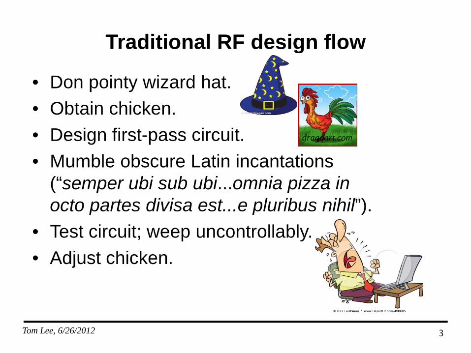
Traditional RF design flowg
• Don pointy wizard hat.• Obtain chicken.• Design first-pass circuit. dragoart.com
• Mumble obscure Latin incantations (“semper ubi sub ubi...omnia pizza in octo partes di isa est e pl rib s nihil”)octo partes divisa est...e pluribus nihil”).
• Test circuit; weep uncontrollably.Adj t hi k• Adjust chicken.
3Tom Lee, 6/26/2012
Dark secrets: A partial listp
• MOSFETs: What your textbook didn’t tell youMOSFETs: What your textbook didn t tell you• The two-port noise model: Why care?
• Optimum noise figure vs. maximum gainOptimum noise figure vs. maximum gain• To match or not to match – that is the question• Linearity and time-invariance revisitedLinearity and time invariance revisited• Mixers: Myths and noise• Strange impedance behaviors (SIBs)• Strange impedance behaviors (SIBs)
4Tom Lee, 6/26/2012
MOSFETs: What Your Textbooks May Not Have Told You
5Tom Lee, 6/26/2012
The standard lie
• “Gate-source impedance is a capacitor.”
• Because zero power is thus needed to drive it, anyoutput at all at any frequency implies infiniteoutput at all, at any frequency, implies infinite power gain. (The books usually omit that last part.)
6Tom Lee, 6/26/2012
The true storyy
• Gate-source impedance is not a pure capacitor.
• Phase shift associated with finite carrier transit d t fi ld d kspeed means gate field does nonzero work on
channel charge.
• Therefore, power gain is not infinite.
• There is also noise associated with the dissipation.
7Tom Lee, 6/26/2012
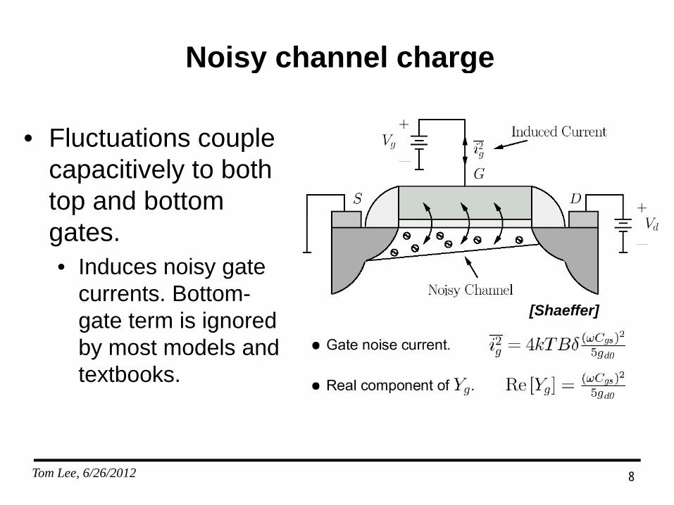
Noisy channel charge
• Fluctuations couple
y g
Fluctuations couple capacitively to both top and bottom gates.• Induces noisy gate
t B ttcurrents. Bottom-gate term is ignored by most models and
[Shaeffer]
textbooks.
8Tom Lee, 6/26/2012

Sources of noise in MOSFETs
• (Thermally agitated) channel charge• (Thermally-agitated) channel charge.• Produces both drain and gate current noise.
• Interconnect resistance.• Series gate resistance R is very importantSeries gate resistance Rg is very important.
• Substrate resistance.Substrate resistance.• Substrate thermal noise modulates back gate,
augments drain current noise in some frequency range.
9Tom Lee, 6/26/2012
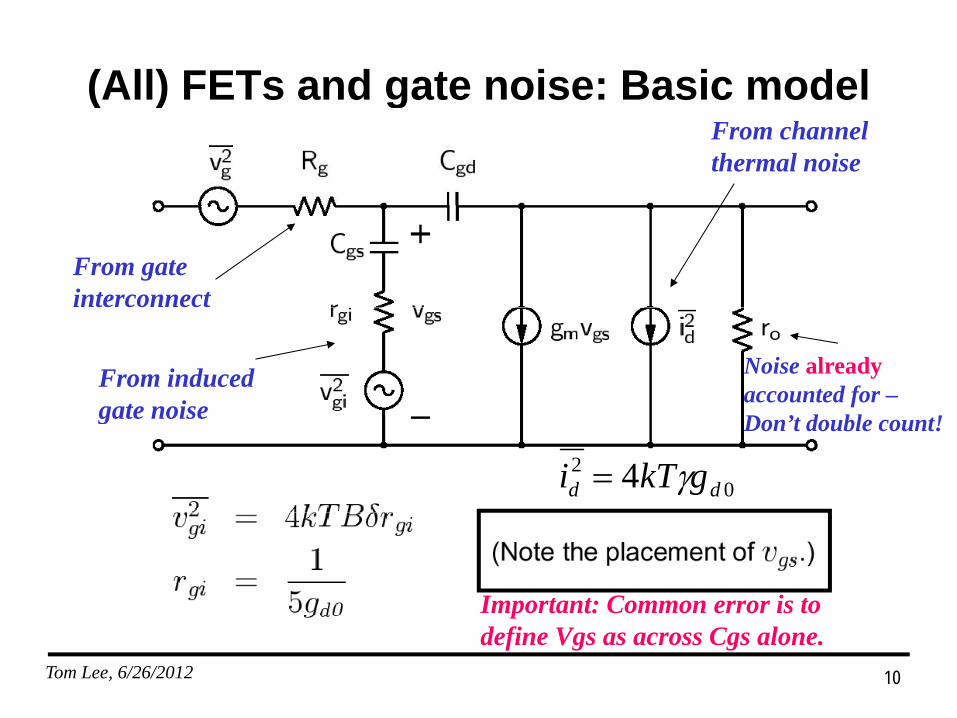
(All) FETs and gate noise: Basic model( ) gFrom channelthermal noise
From gateinterconnect
From inducedgate noise
Noise alreadyaccounted for –gate noise Don’t double count!
02 4 dd gkTi
Important: Common error is to
10Tom Lee, 6/26/2012
pdefine Vgs as across Cgs alone.
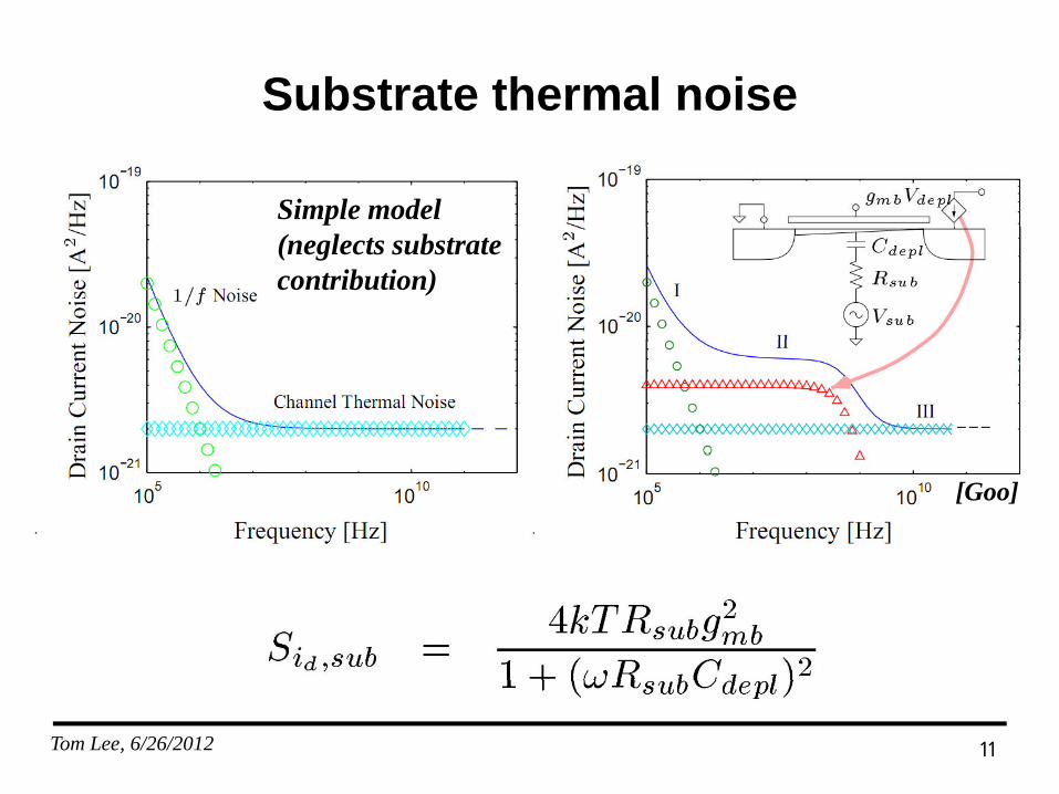
Substrate thermal noise
Simple model(neglects substratecontribution)
[Goo]
11Tom Lee, 6/26/2012
Substrate thermal noise controversyy
• Measuring drain noise at different frequencies• Measuring drain noise at different frequencies has led to confusion about the value of .• Measurements made below ~1GHz (i e in Region II)Measurements made below 1GHz (i.e., in Region II)
may reveal “excess” noise, and a sensitivity to the number of substrate taps, if wrong model is used.
• Early speculations that deep-submicron MOSFET ff f i ifi t h t fMOSFETs suffer from significant enhancement of not borne out.
12Tom Lee, 6/26/2012
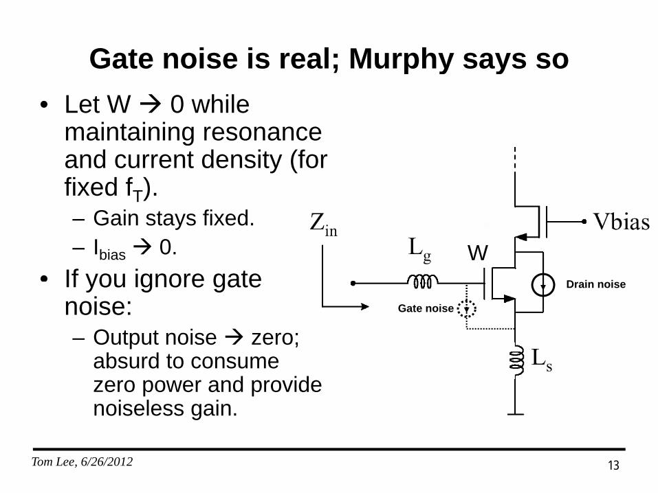
Gate noise is real; Murphy says so• Let W 0 while
maintaining resonance
; p y y
gand current density (for fixed fT).
G i t fi d
D i i
W– Gain stays fixed.– Ibias 0.
• If you ignore gate Drain noise
Gate noise
If you ignore gate noise:– Output noise zero;
absurd to consume zero power and provide noiseless gain.
13Tom Lee, 6/26/2012

The Two-Port Noise Model:The Two-Port Noise Model: Why Care?
14Tom Lee, 6/26/2012
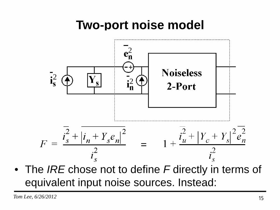
Two-port noise modelp
2
2 2
=
• The IRE chose not to define F directly in terms of i l t i t i I t d
15Tom Lee, 6/26/2012
equivalent input noise sources. Instead:
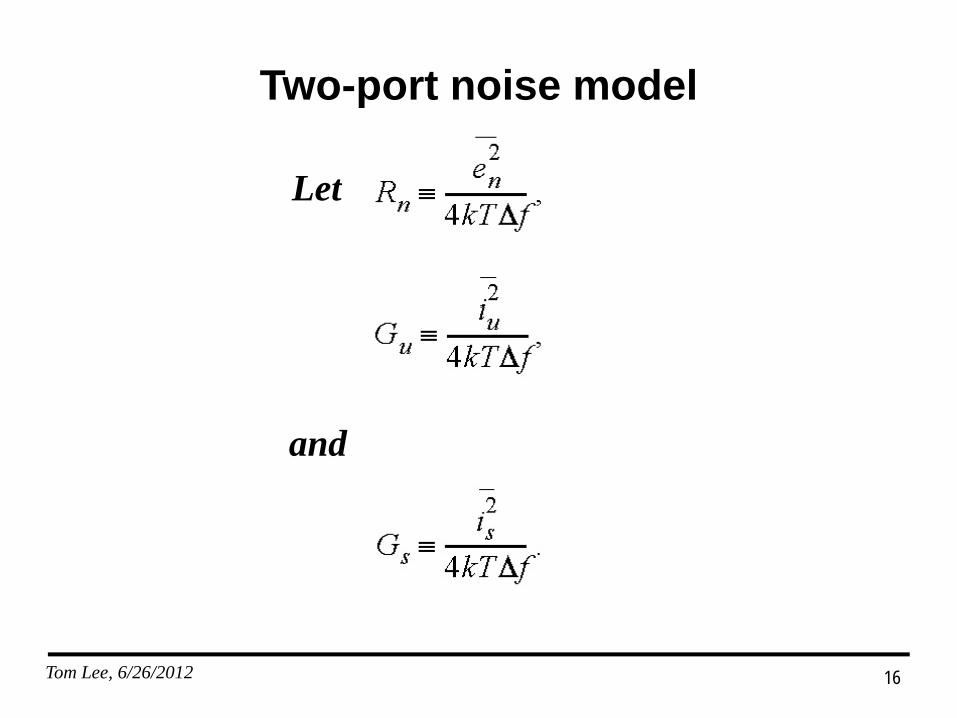
Two-port noise modelp
Let
and
16Tom Lee, 6/26/2012
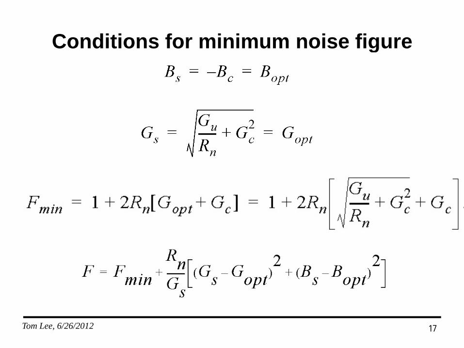
Conditions for minimum noise figureg
17Tom Lee, 6/26/2012
Important observationp• Minimum NF and maximum power gain occur
for the same source Z only if three miraclesfor the same source Z only if three miracles occur together:• Gc = 0 (noise current has no component in phase c ( p p
with noise voltage); and
G G ( d t ti l t d• Gu = Gn (conductance representing uncorrelated current noise equals the fictitious conductance that produces noise voltage); andp g );
• Bc = Bin. (correlation susceptance happens to be the
18Tom Lee, 6/26/2012
same as the actual input susceptance)

To Match or Not to Match --That is the Question
19Tom Lee, 6/26/2012
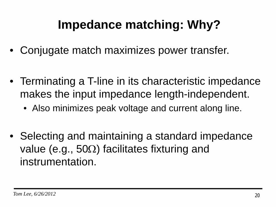
Impedance matching: Why?p g y
• Conjugate match maximizes power transfer.
• Terminating a T-line in its characteristic impedance makes the input impedance length-independent.• Also minimizes peak voltage and current along line.
• Selecting and maintaining a standard impedance value (e g 50) facilitates fixturing andvalue (e.g., 50) facilitates fixturing and instrumentation.
20Tom Lee, 6/26/2012
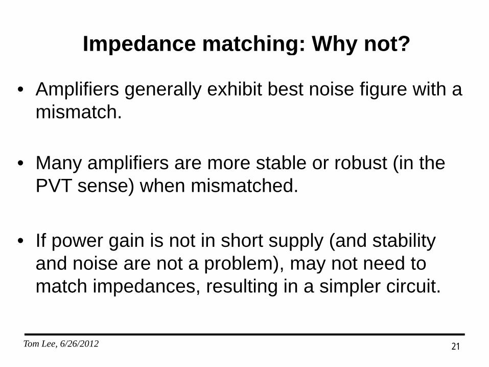
Impedance matching: Why not?p g y
• Amplifiers generally exhibit best noise figure with a i hmismatch.
M lifi t bl b t (i th• Many amplifiers are more stable or robust (in the PVT sense) when mismatched.
• If power gain is not in short supply (and stability and noise are not a problem) may not need toand noise are not a problem), may not need to match impedances, resulting in a simpler circuit.
21Tom Lee, 6/26/2012
Linearity and Time-Invariance:Linearity and Time-Invariance: So What?
22Tom Lee, 6/26/2012
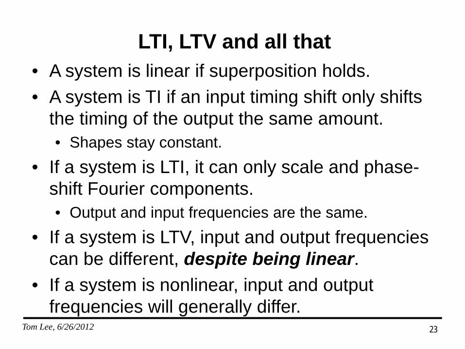
LTI, LTV and all that,• A system is linear if superposition holds.• A system is TI if an input timing shift only shiftsA system is TI if an input timing shift only shifts
the timing of the output the same amount.• Shapes stay constant.p y
• If a system is LTI, it can only scale and phase-shift Fourier components.• Output and input frequencies are the same.
• If a system is LTV, input and output frequencies can be different, despite being linear.
• If a system is nonlinear, input and output
23Tom Lee, 6/26/2012
frequencies will generally differ.
Mixers are supposed to be linear!pp• But they are time-varying blocks.
• Ignore textbooks and papers that say “mixers are• Ignore textbooks and papers that say mixers are nonlinear…” Mixers are nonlinear in the same way amplifiers are nonlinear: Undesirably.
• Significantly noisier than LNAs for reasons that will be explained shortly. NF values of 10-15dB are not unusual.
• Main function of an LNA is usually to provide h i t i i
24Tom Lee, 6/26/2012
enough gain to overcome mixer noise.
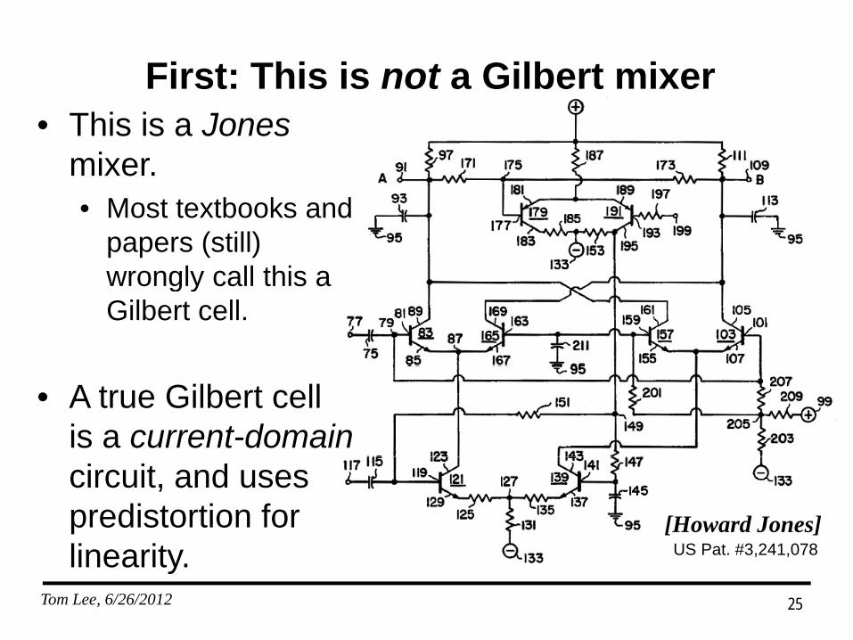
First: This is not a Gilbert mixer• This is a Jones
mixer.• Most textbooks and
papers (still) wrongly call this awrongly call this a Gilbert cell.
• A true Gilbert cell is a current-domaincircuit, and uses predistortion for li it
[Howard Jones] US Pat #3 241 078
25Tom Lee, 6/26/2012
linearity. US Pat. #3,241,078
The mixer: An LTV element• Whether Gilbert, Jones or Smith, modern mixers
depend on commutation of currents or voltagesdepend on commutation of currents or voltages.
• We idealize mixing as the equivalent of• We idealize mixing as the equivalent of multiplying the RF signal by a square-wave LO.• Single-balanced mixer: RF signal is unipolar.Single balanced mixer: RF signal is unipolar.• Double-balanced mixer: RF signal is DC-free.
• Mixing is ideally linear: Doubling the input (RF) voltage should double the output (IF) voltage.
26Tom Lee, 6/26/2012
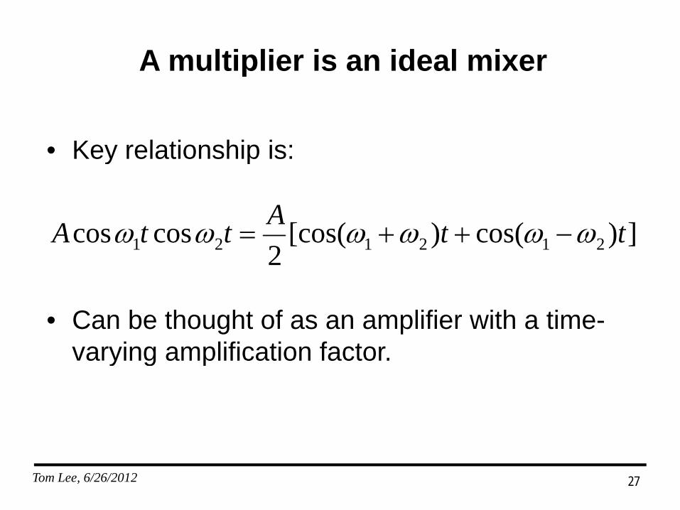
A multiplier is an ideal mixerp
Key relationship is:• Key relationship is:
A ])cos()[cos(2
coscos 212121 ttAttA
• Can be thought of as an amplifier with a time-varying amplification factor.y g p
27Tom Lee, 6/26/2012
Mixer noise figureg
• Noise figure of mixers is worse than for LNAs for• Noise figure of mixers is worse than for LNAs for several reasons.• Noise originating from different RF bands can translateNoise originating from different RF bands can translate
to the same IF. • Transconductor is usually optimized more for linearity
th f ithan for noise.• Switching core contributes significant noise in practical
mixers.mixers.
28Tom Lee, 6/26/2012
Mixer noise figure: DSB v. SSBg
• Because noise from two different sidebands (d i d RF d it i l t d 2f )(desired RF and its image, located 2fIF away) can convert to the same IF, need to be careful about defining NFdefining NF.
• If both sidebands contain signal (and noise) we• If both sidebands contain signal (and noise), we report DSB NF. If signal is present in only one sideband, we report SSB NF.sideband, we report SSB NF.• If noise gains are constant, DSB NF = SSB NF – 3dB.• Because DSB NF is lower, it gets reported more
29Tom Lee, 6/26/2012
frequently. Beware.
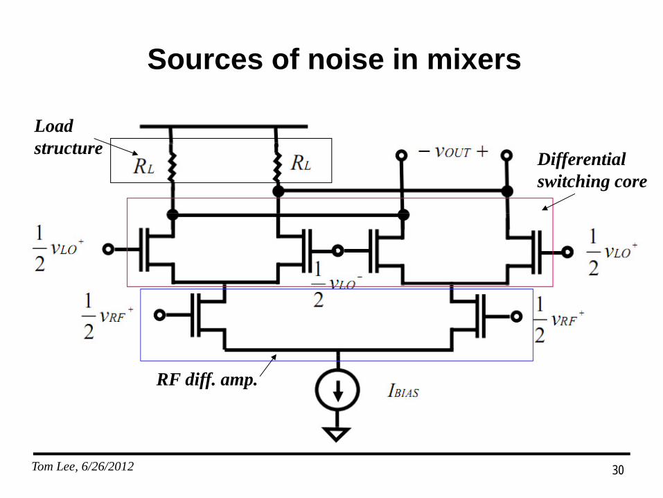
Sources of noise in mixers
Load
Differential switching core
structure
RF diff. amp.
30Tom Lee, 6/26/2012
Mixer noise
• Load structure is at the output so its noise adds to• Load structure is at the output, so its noise adds to the output directly; it undergoes no frequency translations.• If 1/f noise is a concern, use PMOS transistors or poly
resistor loads.
• Transconductor noise appears at same port as i t RF i l it t l t i f thinput RF signal, so it translates in frequency the same way as the RF input.
31Tom Lee, 6/26/2012
Dark secret: Switching noise can dominateg
• Instantaneous switching not possible• Instantaneous switching not possible.• Noise from switching core can actually dominate.• Common-mode capacitance at tail nodes of coreCommon mode capacitance at tail nodes of core
reduces effectiveness of large LO amplitudes.
• Periodic switching of core is equivalent to sampling core noise at (twice) the LO rate.• Frequency translations occur due to this self-mixing.
32Tom Lee, 6/26/2012
Noise contribution of switching coreg
• As switching transistors are driven through the switching instant, they act as a differential pair for a brief window of time ts.
D i thi i t l th it hi t i t t f• During this interval, the switching transistors transfer their drain noise to the output.
• Changing drain current implies a changing PSD for theChanging drain current implies a changing PSD for the noise; it is cyclostationary.
33Tom Lee, 6/26/2012
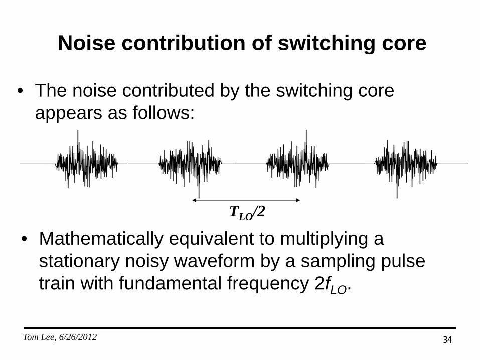
Noise contribution of switching coreg
• The noise contributed by the switching core appears as follows:
T /2
• Mathematically equivalent to multiplying a t ti i f b li l
TLO/2
stationary noisy waveform by a sampling pulse train with fundamental frequency 2fLO.
34Tom Lee, 6/26/2012
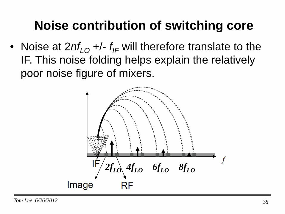
Noise contribution of switching coreg• Noise at 2nfLO +/- fIF will therefore translate to the
IF This noise folding helps explain the relativelyIF. This noise folding helps explain the relatively poor noise figure of mixers.
2fLO 4fLO 6fLO 8fLO
35Tom Lee, 6/26/2012
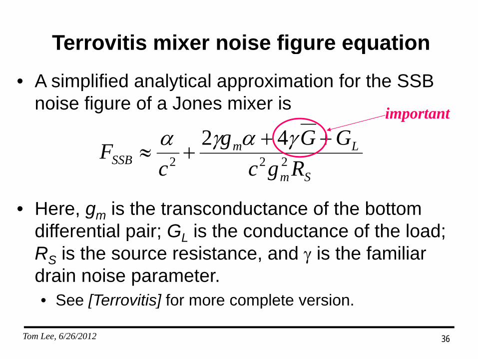
Terrovitis mixer noise figure equationg q
• A simplified analytical approximation for the SSB noise figure of a Jones mixer isnoise figure of a Jones mixer is
Lm GGgF 42
important
SmSSB Rgcc
F 222
Here g is the transcond ctance of the bottom• Here, gm is the transconductance of the bottom differential pair; GL is the conductance of the load; RS is the source resistance and is the familiarRS is the source resistance, and is the familiar drain noise parameter.• See [Terrovitis] for more complete version.
36Tom Lee, 6/26/2012
[ ] p
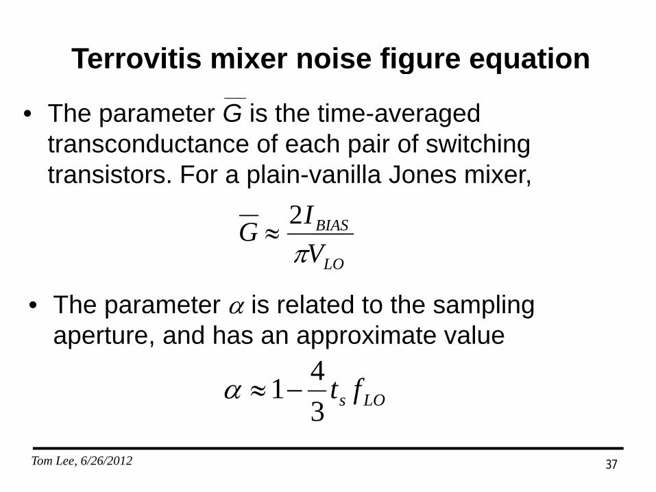
Terrovitis mixer noise figure equationg q
• The parameter G is the time-averaged transconductance of each pair of switchingtransconductance of each pair of switching transistors. For a plain-vanilla Jones mixer,
I2
LO
BIAS
VIG2
• The parameter is related to the sampling aperture, and has an approximate value
LOs ft341
37Tom Lee, 6/26/2012
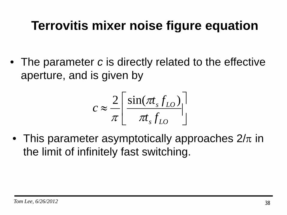
Terrovitis mixer noise figure equationg q
• The parameter c is directly related to the effective• The parameter c is directly related to the effective aperture, and is given by
LOs
LOs
ftftc
)sin(2
LOs f
• This parameter asymptotically approaches 2/ in the limit of infinitely fast switchingthe limit of infinitely fast switching.
38Tom Lee, 6/26/2012
When Good Amplifiers Go Bad:
Strange Impedance Behaviors
39Tom Lee, 6/26/2012
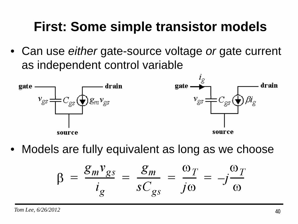
First: Some simple transistor modelsp
• Can use either gate-source voltage or gate current as independent control variableas independent control variable
• Models are fully equivalent as long as we choose
40Tom Lee, 6/26/2012
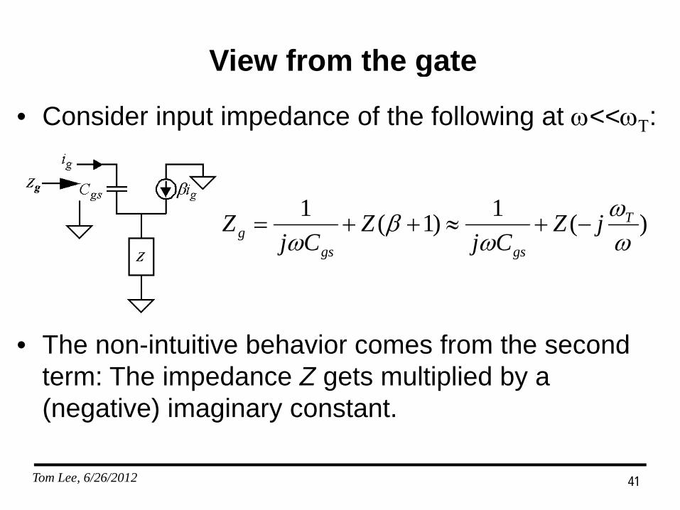
View from the gateg
• Consider input impedance of the following at <<:
)(1)1(1 TjZZZ )()1(
T
gsgsg jZ
CjZ
CjZ
• The non-intuitive behavior comes from the second term: The impedance Z gets multiplied by a (negative) imaginary constant.
41Tom Lee, 6/26/2012

What does multiplication by –jT/ do?p y j T
• Turns R into capacitance of value 1/ R• Turns R into capacitance of value 1/TR.
• Turns L into resistance of value L• Turns L into resistance of value TL.
T C i t ti i t f l / 2C• Turns C into negative resistance of value -T/2C.
42Tom Lee, 6/26/2012
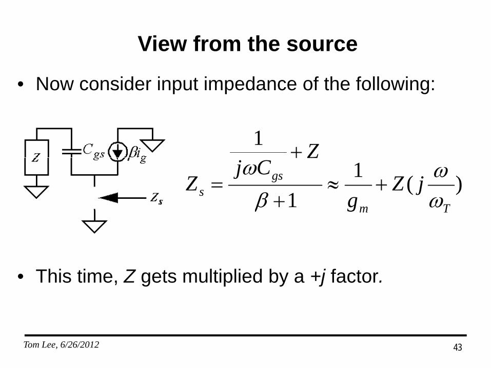
View from the source
• Now consider input impedance of the following:
1 Z)(1
1 Tm
gss jZ
g
ZCj
Z
Tmg
• This time, Z gets multiplied by a +j factor.
43Tom Lee, 6/26/2012
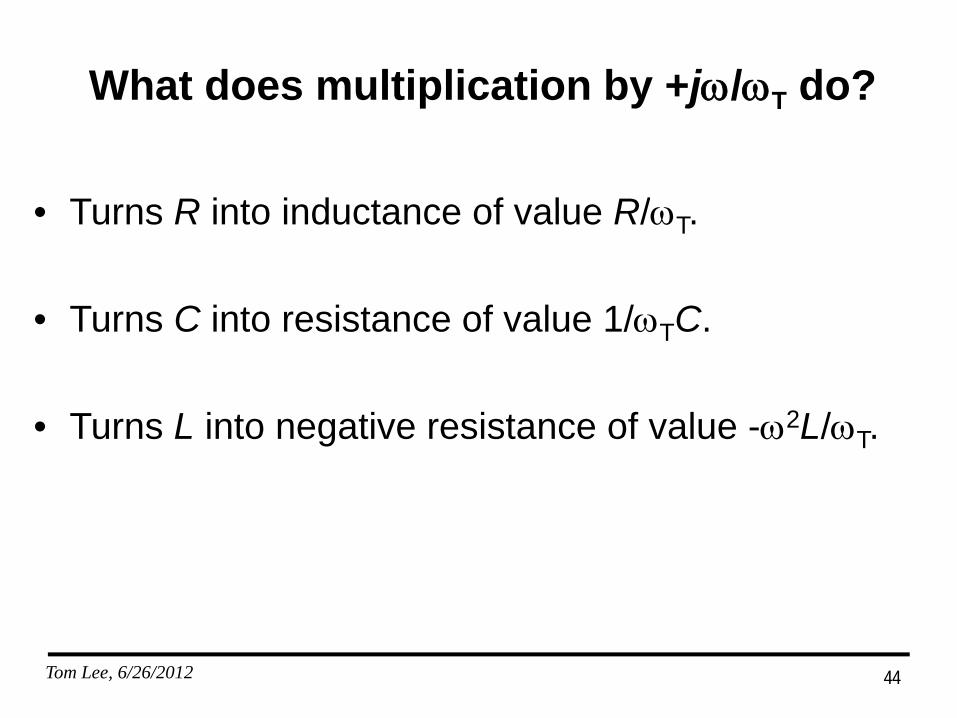
What does multiplication by +j/T do?p y j T
Turns R into inductance of value R/• Turns R into inductance of value R/T.
T C i t i t f l 1/ C• Turns C into resistance of value 1/TC.
2• Turns L into negative resistance of value -2L/T.
44Tom Lee, 6/26/2012
Why SIBs are strangey g
• Apparent weirdness arises because the current gain is imaginarygain is imaginary.
Q d t h hift i t d ith i i• Quadrature phase shift associated with imaginary current gain causes impedances to change character not just magnitudecharacter, not just magnitude.
• The strangeness evaporates once you spend a• The strangeness evaporates once you spend a little time studying where it comes from.
45Tom Lee, 6/26/2012
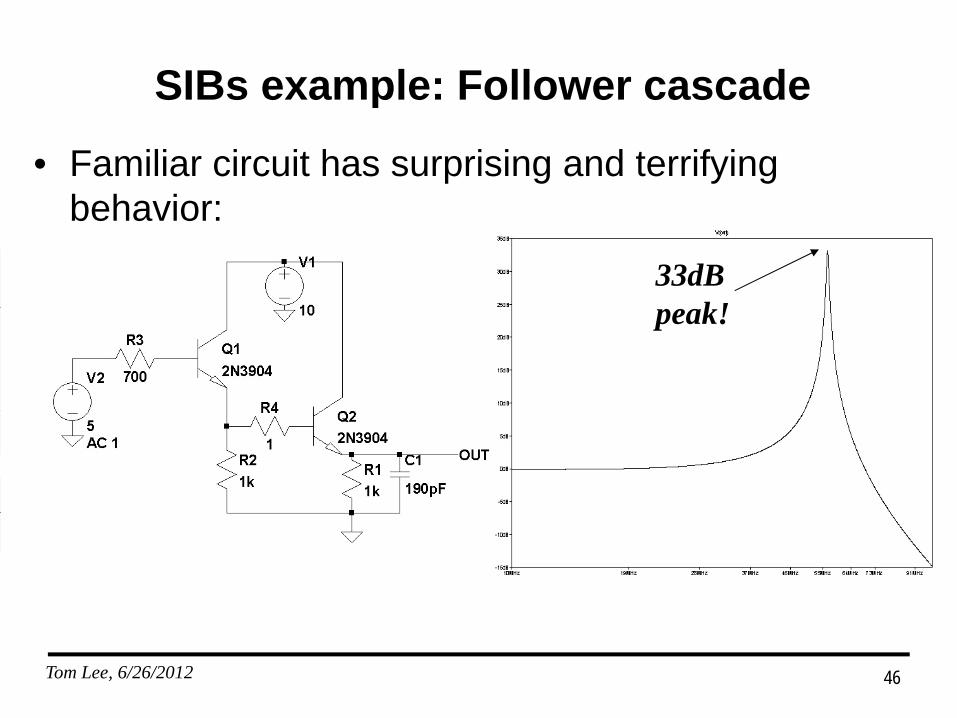
SIBs example: Follower cascadep
• Familiar circuit has surprising and terrifying behavior:behavior:
33dB k!peak!
46Tom Lee, 6/26/2012
Summaryy
• RF circuits are certainly complex but that shouldn’t• RF circuits are certainly complex, but that shouldn t make us concede defeat.
• Everything is explicable; it’s not magic!
• So throw away the pointy hat, free the chickens, quit babbling in Latin, and stop weepingquit babbling in Latin, and stop weeping uncontrollably.
47Tom Lee, 6/26/2012
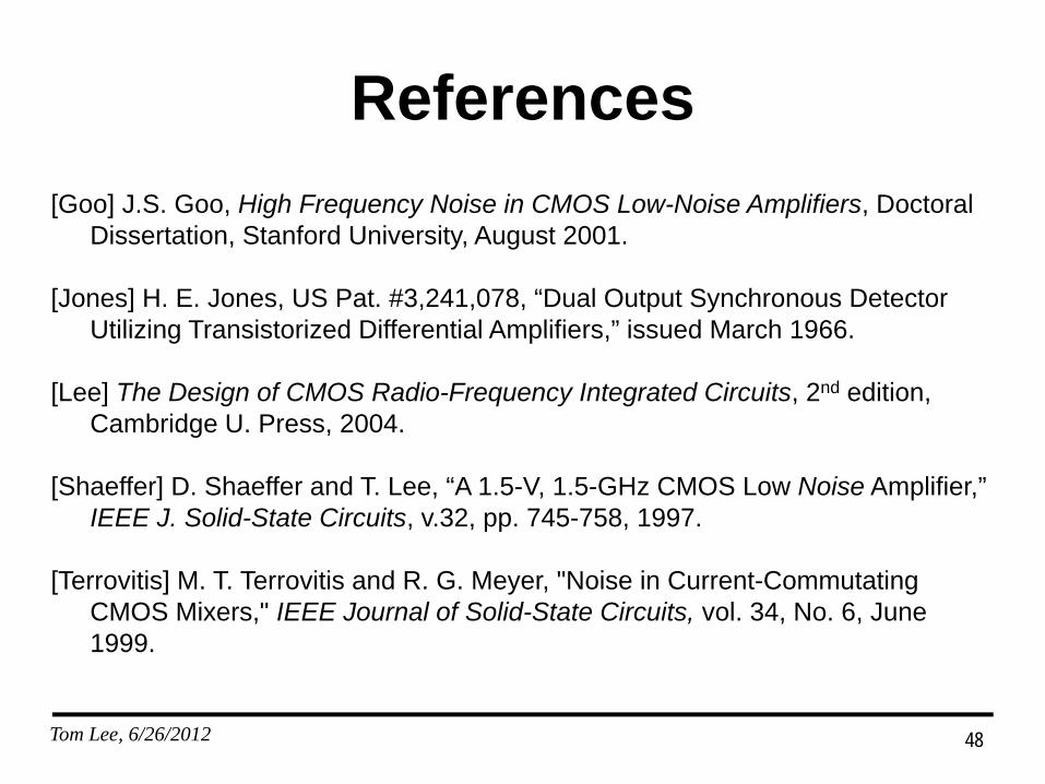
ReferencesReferences[Goo] J.S. Goo, High Frequency Noise in CMOS Low-Noise Amplifiers, Doctoral
Dissertation, Stanford University, August 2001.
[Jones] H. E. Jones, US Pat. #3,241,078, “Dual Output Synchronous Detector Utilizing Transistorized Differential Amplifiers,” issued March 1966.Utilizing Transistorized Differential Amplifiers, issued March 1966.
[Lee] The Design of CMOS Radio-Frequency Integrated Circuits, 2nd edition, Cambridge U. Press, 2004.
[Shaeffer] D. Shaeffer and T. Lee, “A 1.5-V, 1.5-GHz CMOS Low Noise Amplifier,” IEEE J. Solid-State Circuits, v.32, pp. 745-758, 1997.
[Terrovitis] M. T. Terrovitis and R. G. Meyer, "Noise in Current-Commutating CMOS Mixers," IEEE Journal of Solid-State Circuits, vol. 34, No. 6, June 1999.
48Tom Lee, 6/26/2012