Embed Size (px)
Citation preview

ELEKTRONSKI FAKULTET Katedra za mikroelektroniku
0
DIGITALNA MIKROELEKTRONIKA Laboratorijske vežbe
Danijel Danković
Univerzitet u Nišu Elektronski fakultet
Katedra za mikroelektroniku

ELEKTRONSKI FAKULTET Katedra za mikroelektroniku
1
DIGITALNA MIKROELEKTRONIKA Laboratorijske vežbe
I. 7-Segment Display
1. Start the Logisim program. 2. Save Logisim Project. (File->Save), name the project (for example “7-Segment Display”), and choose a safe place for it to be saved. 3. Load Built-in Library (Project->Load Library->Built-in Library->Input/Output). 4. Now build the circuit shown in Fig. 1. First add “7-Segment Display”, OR gate, AND gate, NOT gate, wire and input pin to the schematic. Fig.1
5. Check the output for various values of inputs A, B, C and D.

ELEKTRONSKI FAKULTET Katedra za mikroelektroniku
2
Arrangement of segments for “Seven-segment display”:
Inputs for “Seven-segment display”:
Active segment for each decimal digit:
DIGIT SEGMENTS ACTIVADET 0 a, b, c, d, e, f 1 b, c 2 a, b, d, e, g 3 a, b, c, d, g 4 b, c, f, g 5 a, c, d, f, g 6 a, c, d, e, f, g 7 a, b, c 8 a, b, c, d, e, f, g 9 a, b, c, d, f, g
Block diagram of 7-segment logic and display:

ELEKTRONSKI FAKULTET Katedra za mikroelektroniku
3
Truth table for 7-segment logic:
DECIMAL DIGIT
INPUTS D C B A
SEGMENT OUTPUTS a b c d e f g
0 0 0 0 0 1 1 1 1 1 1 0 1 0 0 0 1 0 1 1 0 0 0 0 2 0 0 1 0 1 1 0 1 1 0 1 3 0 0 1 1 1 1 1 1 0 0 1 4 0 1 0 0 0 1 1 0 0 1 1 5 0 1 0 1 1 0 1 1 0 1 1 6 0 1 1 0 1 0 1 1 1 1 1 7 0 1 1 1 1 1 1 0 0 0 0 8 1 0 0 0 1 1 1 1 1 1 1 9 1 0 0 1 1 1 1 1 0 1 1 10 1 0 1 0 X X X X X X X 11 1 0 1 1 X X X X X X X 12 1 1 0 0 X X X X X X X 13 1 1 0 1 X X X X X X X 14 1 1 1 0 X X X X X X X 15 1 1 1 1 X X X X X X X
Karnaugh map minimization of the segment-a logic expresion: Standard SOP expression:
ABCDABCDCBADACBDABCDBACDABCDABCD +++++++ Minimum SOP expression:
ACCABD +++ The minimum logic implementation for segment a of the 7-segment display:

ELEKTRONSKI FAKULTET Katedra za mikroelektroniku
4
Karnaugh map minimization: 1. Start the Karnaugh Map Minimizer program. 2. Set truth table. Move the cursor over blue “f” box. Press <RightMouseButton> and a dialog box will appear. Choose “Set to 1”, “Set to 0” or “Set don’t care”. 3. For type of solution use “Sum of products”. 4. Press the “Solve” key button and minimum SOP expression will appear (Fig. 2). Fig.2
ELEKTRONSKI FAKULTET Katedra za mikroelektroniku
5
DIGITALNA MIKROELEKTRONIKA Laboratorijske vežbe
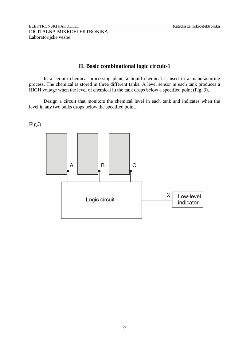
II. Basic combinational logic circuit-1
In a certain chemical-processing plant, a liquid chemical is used in a manufacturing process. The chemical is stored in three different tanks. A level sensor in each tank produces a HIGH voltage when the level of chemical in the tank drops below a specified point (Fig. 3).
Design a circuit that monitors the chemical level in each tank and indicates when the level in any two tanks drops below the specified point. Fig.3

ELEKTRONSKI FAKULTET Katedra za mikroelektroniku
6
1. Write the truth table for logic circuit:
INPUTS A B C
LOW-LEWEL INDICATOR
0 0 0 0 0 0 1 0 0 1 0 0 0 1 1 1 1 0 0 0 1 0 1 1 1 1 0 1 1 1 1 1
2. Start the Karnaugh Map Minimizer program. 3. Set truth table. 4. For type of solution use “Sum of products”. 4. Press the “Solve” key button and minimum SOP expression will appear (Fig. 4). Fig.4
Minimum SOP expression:
BCACAB ++

ELEKTRONSKI FAKULTET Katedra za mikroelektroniku
7
1. Start the Logisim program. 2. Save Logisim Project. (File->Save), name the project (for example “Basic combinational logic circuit-1”), and choose a safe place for it to be saved. 3. Load Built-in Library (Project->Load Library->Built-in Library->Input/Output). 4. Now build the circuit shown in Fig. 5. Fig.5

ELEKTRONSKI FAKULTET Katedra za mikroelektroniku
8
DIGITALNA MIKROELEKTRONIKA Laboratorijske vežbe
III. Basic combinational logic circuit-2
The sensors in the chemical tanks of Example II. are being replaced by a new model that produces a LOW voltage instead of a HIGH voltage when the level of the chemical in the tank drops below a specified point (Fig. 6).
Modify the circuit in in Fig. 5 to operate with the different input levels and still produce a HIGH output to activate the indicator when the level in any two of the tanks drops below the critical point.
Show the logic diagram.
Fig.6

ELEKTRONSKI FAKULTET Katedra za mikroelektroniku
9
Solution
The AND-OR-Invert circuit has inputs from the sensors on tank A, B and C as shown in Fig. 7. The AND gate G1 checks the levels in tanks A and B, gate G2 checks tank A and C, and gate G3 checks tanks B and C. When the chemical level in any two of the tanks gets too low, each AND gate will have a LOW on at least one input causing its output to be LOW and, thus, the final output X from the inverter is HIGH. This HIGH output is then used to activate an indicator. Fig.7

ELEKTRONSKI FAKULTET Katedra za mikroelektroniku
10
DIGITALNA MIKROELEKTRONIKA Laboratorijske vežbe
IV. The Half-Adder
The half-adder accepts two binary digits on its inputs and produces two binary digits on its outputs, a sum bit and a carry bit. A half-adder is represented by the logic symbol in Fig. 8. Fig.8
Half-Adder Logic: We can see half-adder truth table. Using the data from truth table expressions can be derived for the sum and the uotput carry as functions of the inputs.
A B Cout ∑ 0 0 0 0 0 1 0 1 1 0 0 1 1 1 1 0
Notice that the output carry (Cout) is a 1 only when both A and B are 1s; therefore, Cout can be expressed as the AND of the input variables: Cout = AB Now observe that the sum output (∑) is a 1 only if the input variables, A and B, are not equal. The sum can therefore be expressed as the exclusive-OR of the input variables. ∑ = A ⊕ B The logic implementation requred for the half-adder function can be developed. 1. Start the Logisim program. 2. Save Logisim Project. (File->Save), name the project (for example “The Half-Adder”), and choose a safe place for it to be saved. 3. Now build the circuit shown in Fig. 9. Fig.9

ELEKTRONSKI FAKULTET Katedra za mikroelektroniku
11
DIGITALNA MIKROELEKTRONIKA Laboratorijske vežbe
V. The Full-Adder
The full-adder accepts two input bits and an input carry and generates a sum output and an output carry. A full-adder is represented by the logic symbol in Fig. 10. Fig.10
Full-Adder Logic: We can see full-adder truth table. Using the data from truth table expressions can be derived for the sum and the uotput carry as functions of the inputs.
A B C Cout ∑ 0 0 0 0 0 0 0 1 0 1 0 1 0 0 1 0 1 1 1 0 1 0 0 0 1 1 0 1 1 0 1 1 0 1 0 1 1 1 1 1
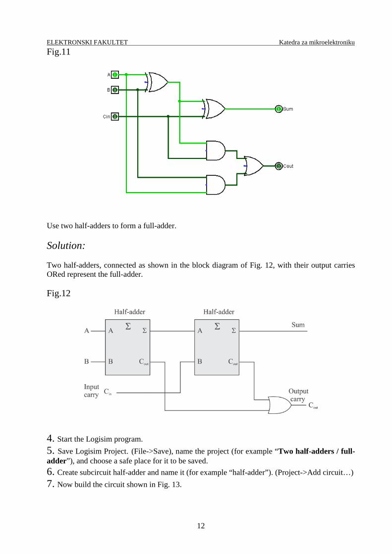
From the half-adder we know that the sum of the input bits A and B is the exclusive-OR of those two variables, A ⊕ B. For the input carry (Cin) to be added to the input bits, it must be exclusive ORed with A ⊕ B, yielding the equation for the sum output of the full-adder: ∑ = (A ⊕ B) ⊕ Cin This means that to implement the full-adder sum function, two 2-input exclusive-OR gates can be used. The first must generate the term A ⊕ B, and the second has as its inputs the output of the first XOR gate and the input carry. The output carry of the full-adder is produced by the inputs A ANDed with B and A ⊕ B ANDed with Cin. These two terms are ORed, as expressed in equation Cout = AB+(A ⊕ B) Cin This function is implemented and combined with the sum logic to form a complete full-adder circuit, as shown in Fig. 11. 1. Start the Logisim program. 2. Save Logisim Project. (File->Save), name the project (for example “The Full-Adder”), and choose a safe place for it to be saved. 3. Now build the circuit shown in Fig. 11.
ELEKTRONSKI FAKULTET Katedra za mikroelektroniku
12
Fig.11
Use two half-adders to form a full-adder. Solution: Two half-adders, connected as shown in the block diagram of Fig. 12, with their output carries ORed represent the full-adder. Fig.12
4. Start the Logisim program. 5. Save Logisim Project. (File->Save), name the project (for example “Two half-adders / full-adder”), and choose a safe place for it to be saved. 6. Create subcircuit half-adder and name it (for example “half-adder”). (Project->Add circuit…) 7. Now build the circuit shown in Fig. 13.

ELEKTRONSKI FAKULTET Katedra za mikroelektroniku
13
Fig.13

ELEKTRONSKI FAKULTET Katedra za mikroelektroniku
14
DIGITALNA MIKROELEKTRONIKA Laboratorijske vežbe
VI. Parallel binary adders
Two or more full-adders can be connected to form parallel binary adders. A single full-adder is capable of adding two 1-bit numbers and an input carry. To add binary numbers with more than one bit, you must use additional full-adders. When one binary number is added to another, each column generates a sum bit and a 1 or 0 carry bit to the next column to the left, as illustrated in Fig. 14 with 2-bit numbers. Fig.14
To add two binary numbers, a full-adder is required for each bit in the numbers. So for 2-bit numbers, two adders are needed; for 4-bit numbers, four adders are used; and so on. The carry output of each adder is connected to the carry input of the next higher-order adder. Either a half-adder can be used for the least significant position or the carry input of a full-adder can be made 0 (grounded) because there is no carry in the least significant bit position.
Four-Bit Parallel Adders: A group of four bits is called a nibble. A basic 4-bit parallel adder is implemented with four full-adder stages as shown in Fig. 15. Fig.15
ELEKTRONSKI FAKULTET Katedra za mikroelektroniku
15
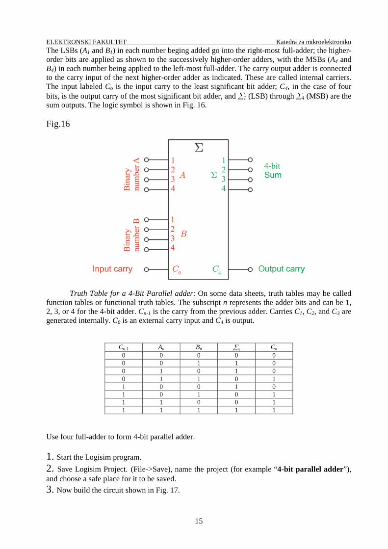
The LSBs (A1 and B1) in each number beging added go into the right-most full-adder; the higher-order bits are applied as shown to the successively higher-order adders, with the MSBs (A4 and B4) in each number being applied to the left-most full-adder. The carry output adder is connected to the carry input of the next higher-order adder as indicated. These are called internal carriers. The input labeled Co is the input carry to the least significant bit adder; C4, in the case of four bits, is the output carry of the most significant bit adder, and ∑1 (LSB) through ∑4 (MSB) are the sum outputs. The logic symbol is shown in Fig. 16. Fig.16
Truth Table for a 4-Bit Parallel adder: On some data sheets, truth tables may be called function tables or functional truth tables. The subscript n represents the adder bits and can be 1, 2, 3, or 4 for the 4-bit adder. Cn-1 is the carry from the previous adder. Carries C1, C2, and C3 are generated internally. C0 is an external carry input and C4 is output.
Cn-1 An Bn ∑n Cn 0 0 0 0 0 0 0 1 1 0 0 1 0 1 0 0 1 1 0 1 1 0 0 1 0 1 0 1 0 1 1 1 0 0 1 1 1 1 1 1
Use four full-adder to form 4-bit parallel adder. 1. Start the Logisim program. 2. Save Logisim Project. (File->Save), name the project (for example “4-bit parallel adder”), and choose a safe place for it to be saved. 3. Now build the circuit shown in Fig. 17.

ELEKTRONSKI FAKULTET Katedra za mikroelektroniku
16
4. Use the 4-bit parallel adder to find the sum and output carry for the following two 4-bit numbers if the input carry (Cn-1) is 0: A4A3A2A1 = 1100 and
B4B3B2B1 = 1100 Fig.17
As can be seen from Fig. 17, the sum of 1100 and 1100 is 11000.

ELEKTRONSKI FAKULTET Katedra za mikroelektroniku
17
DIGITALNA MIKROELEKTRONIKA Laboratorijske vežbe
VII. The 74LS283 4-bit parallel adder
The 74LS283 is a 4-bit parallel adder that is available in IC form. The pin diagram and logic symbol are shown in Figs. 18 and 19. For the 74LS283, VCC is pin 16 and ground is pin 8, which is a standard configuration. Fig.18 Fig.19
Adder expansion: The 4-bit parallel adder can be expanded to handle the addition of two 8-bit numbers using two 4-bit adders. The carry input of the low-order adder (C0) is connected to ground because there is no carry into the least significant bit position, and the carry output of the low-order adder is connected to the carry input of high-order adder. This process is known as cascading. The low-order adder is the one that adds the lower or less significant four bits in he numbers, and the high-order adder is the one that adds the higher more significant four bits in the 8-bit numbers.
Similarly, four 4-bit adders can be cascaded to handle two 16-bit numbers.
Use 74LS283 parallel adders to form 8-bit adder. Show the 8-bit adder with proper interconnections.

ELEKTRONSKI FAKULTET Katedra za mikroelektroniku
18
Solution
Two 74LS283 parallel adders are used to implement the 8-bit adder. They are connected as shown in Fig. 20 in a cascaded arrangement. The only connection between the two 74LS283s is the carry output (pin 9) of the lower-order adder to the carry input (pin 7) of the high-order adder, as shown in Fig. 20. Pin 7 of the low-order adder is grounded (no carry input). Fig.20

ELEKTRONSKI FAKULTET Katedra za mikroelektroniku
19
DIGITALNA MIKROELEKTRONIKA Laboratorijske vežbe
VIII. The 74HC85 4-bit magnitude comparator
The 74HC85 is a comparator that is also available in other IC families. The pin diagram and logic symbol are shown in Figs. 21 and 22. Notice that this device has three cascading inputs: A<B, A=B and A>B. These inputs allow several comparators to be cascaded for comparison of any number of bits greater than four. To expand the comparator, the A<B, A=B and A>B outputs of the lower-order comparator are connected to the corresponding inputs of the next higher-order comparator. The lowest-order comparator must have a HIGH on the A=B input and LOWs on the A<B and A>B inputs. Fig.21 Fig.22
Use 74HC85 comparators to compare the magnitudes of two 8-bit numbers. Show the comparators with proper interconnections.

ELEKTRONSKI FAKULTET Katedra za mikroelektroniku
20
Solution
Two 74HC85s are required to compare two 8-bit numbers. They are connected as shown in Fig. 23 in a cascaded arrangement. Fig.23

ELEKTRONSKI FAKULTET Katedra za mikroelektroniku
21
DIGITALNA MIKROELEKTRONIKA Laboratorijske vežbe
IX. The 74LS47 BCD-to-7-segment decoder/driver
The 74LS47 is an example of an IC device that decodes a BCD input and drives a 7-segment display. In addition to its decoding and segment drive capability, the 74LS47 has several additional features as indicated by the LT , RBI , BI / RBO functions in the logic symbol of Figs. 24 and 25. As indicated by the bubbles on the logic symbol, all of the outputs (a through g) are active-LOW as are the LT (lamp test), RBI (ripple blanking input), and BI / RBO (blanking input/ripple blanking output) functions. The outputs can drive a common-anode 7-segment display directly. Fig.24 Fig.25
Use the 74LS47 BCD-to-7-segment decoder/driver for multidigit displays to blank out
unnecessary zeros. For example, in a 6-digit display the number 6.4 may be displayed as 006.400 if the zeros are not blanked out. Blanking the zeros at the front of number is called leading zero suppression and blanking the zeros at the back of the number is called trailing zero suppresion. Keep in mind that only nonessential zeros are blanked.

ELEKTRONSKI FAKULTET Katedra za mikroelektroniku
22
Solution
Logic diagram for 74LS47 BCD-to-7-segment decoder/driver:
1. Start the Logisim program. 2. Save Logisim Project. (File->Save), name the project (for example “Leading zero suppression”), and choose a safe place for it to be saved. 3. Create subcircuit 74LS47 BCD-to-7-segment decoder/driver and name it (for example “74LS47_TI”). 4. Now build the circuit shown in Fig. 26.
The highest-order digit position (left-most) is always blanked if a zero code is on its BCD inputs because the RBI of the most-significant decoder is made LOW by connecting it to ground. The RBO of each decoder is connected to the RBI of the next lowest-order decoder so that all zeros to the left of the first nonzero digit are blanked.

ELEKTRONSKI FAKULTET Katedra za mikroelektroniku
23
Fig.26
5. Start the Logisim program. 6. Save Logisim Project. (File->Save), name the project (for example “Trailing zero suppression”), and choose a safe place for it to be saved. 7. Now build the circuit shown in Fig. 27.
The lowest-order digit position (right-most) is always blanked if a zero code is on its BCD inputs because the RBI is connecting to ground. The RBO of each decoder is connected to the RBI of the next highest-order decoder so that all zeros to the right of the first nonzero digit are blanked. Fig.27

ELEKTRONSKI FAKULTET Katedra za mikroelektroniku
24
Both leading and trailing zero suppression in one display is shown in Fig. 28. Fig.28

ELEKTRONSKI FAKULTET Katedra za mikroelektroniku
25
DIGITALNA MIKROELEKTRONIKA Laboratorijske vežbe
X. A 7-Segment Display Multiplexer
In this example, 2-digit numbers are displayed on the 7-segment readout by the use of a single BCD-to-7-segment decoder. This basic method of display multiplexing can be extended tp displays with any number of digits. 1. Start the Logisim program. 2. Save Logisim Project. (File->Save), name the project (for example “A 7-Segment Display Multiplexer”), and choose a safe place for it to be saved. 3. Create subcircuit 74LS157 2-input data selector/miltiplexer and name it (for example “74LS157”). 4. Create subcircuit 74LS139 dual 2-line to 4-line decoders/demultiplexers and name it (for example “74LS139/2”). 5. Create subcircuit 74LS465 buffer and name it (for example “74LS465”). 6. Set up the frequency to 16 Hz (Simulate->Tick Frequency->16 Hz). 7. Now build the circuit shown in Fig. 29.
The basic operation is as follows. Two BCD digits (A4A3A2A1 and B4B3B2B1) are applied to the multiplexer inputs. A square wave is applied to the data-select line, and when it is LOW, the A bits (A4A3A2A1) are passed through to the inputs of the 74LS47 BCD-to-7-segment decoder. The LOW on the data-select also puts a LOW on the A1 input of the 74LS139 2-line-to-4-line decoder, thus activating its 0 input and enabling the A-digit display by effectively connecting its common terminal to ground. The A digit is now on and the B digit is off.
When the data-select line goes HIGH, the B bits (B4B3B2B1) are passed through to the inputs of the BCD-to-7-segment decoder. Also, the 74LS139 decoder’s 1 output is activated, thus enabling the B-digit display. The B digit is now on and the A digit is off. The cycle repeats at the frequency of the data-select square wave. This frequency must be high enough (about 30 Hz) to prevent visual flicker as the digit display are multiplexed.

ELEKTRONSKI FAKULTET Katedra za mikroelektroniku
26
Fig.29

ELEKTRONSKI FAKULTET Katedra za mikroelektroniku
27
DIGITALNA MIKROELEKTRONIKA Laboratorijske vežbe
XI. Traffic light control system/combinational logic
General System Requirements: A digital controller is required to control a traffic light at the intersection of a busy main street and an occasionally used side street. The main street is to have a green light for a minimum of 25 s or as long as there is no vehicle on the side street. The side street is to have a green light until there is no vehicle on the side street or for a maximum of 25 s. There is to be a 4 s caution light (yellow) between changes from green to red on both the main street and on the side street. These requirements are illustrated in the pictorial diagram in Fig. 30. Fig.30
First state: 25 seconds Second state: 4 seconds Third state: 25 seconds Fourth state: 4 seconds minimum or as long as maximum or until there there is no vehicle is no vehicle on side street on side street Developing a Block Diagram of the System: System must control six different pairs of lights. These are the red, yellow and green lights for both directions on the main street and the red, yellow and green lights for both directions on the side street. Also, there is one external input (other than power) from a side street vehicle sensor. Fig. 31 is a minimal block diagram showing these requirements. The system has four states, as indicated in Fig. 30, so a logic circuit is needed to control the sequence of states (sequential logic). Also, circuits are needed to generate the proper time intervals of 25 s and 4 s that are required in the system and to generate a clock signal for cycling the system (timing circuit). The time intervals (long and short) and the vehicle sensor are inputs to the sequential logic because the sequencing of states is a function of these variables. Logic circuits are also needed to determine which of four states the system is in at any given time, to generate the proper outputs to the light (state decoder and light output logic), and to initiate the long and short time interval. Interface circuits are included in the traffic light and interface unit to convert the output levels of the light output logic to the voltages and currents required to turn on each of the lights. Fig. 32 is a more detailed block diagram showing these essential elements.

ELEKTRONSKI FAKULTET Katedra za mikroelektroniku
28
Fig.31
Fig.32
The State Diagram: A state diagram graphically shows the sequence of states in a system and the conditions for each state and for transitions from one state to the next. Actually, Fig. 30 is a form of state diagram because it shows the sequence of states and the conditions. Definition of Variables: Before a traditional state diagram can be developed, the variables that determine how the system sequences through its states must be defined. These variables and their symbols are listed as follows:
• Vehicle present on side street = VS • 25 s timer (long timer) is on = TL • 4 s timer (short timer) is on = TS

ELEKTRONSKI FAKULTET Katedra za mikroelektroniku
29
The use of complemented variables indicates the opposite conditions. For example, SV indicates
that there is no vehicle on the side street, LT indicates the long timer is off, ST indicates the short timer is off.
Description of the State Diagram: A state diagram is shown in Fig. 33. Each of the four
states is labeled according to the 2-bit Gray code sequence, as indicated by the circles. The looping arrow at each state indicates that the system remains in that state under the condition defined by the associated variable or expression. Each of the arrows going from one state to the next indicates a state transition under the condition defined by the associated variable or expression.
Fig.33
The Gray code for first state is 00. The main street light is green and the side street light is red. The system remains in this state for at least 25 s when the long timer is on or as long as there is no vehicle on the side street (TL + SV ). The system goes to the next state when 25 s timer is off
and there is a vehicle on the side street ( LT ⋅VS). We have a similar analysis in the case of second, third and fourth state.

ELEKTRONSKI FAKULTET Katedra za mikroelektroniku
30
The Combinational Logic: A block diagram for the combinational logic portion of the system is developed as the first step. The three functions that this logic must perform are defined as follows, and the resulting diagram with a block for each of the three functions is shown in Fig. 34.
• State Decoder Decodes the 2-bit Gray code from the sequential logic to determine which of the four states the system is in.
• Light Output Logic Uses the decoded state to activate the appropriate traffic lights for the main and side street light units.
• Trigger Logic Uses the decoded states to produce signals for properly initiating (triggering) the long timer and the short timer.
Fig.34
Implementation of the Combinational Logic: a) Implementing the Decoder Logic: The state decoder portion has two inputs
(2−bit Gray code) and an output for each of the four states. The two Gray code inputs are designated S0 and S1 and the four state outputs are labeled SO1, SO2, SO3 and SO4. The Boolean expressions for the state outputs are as follows:
SO1 = 1S 0S SO2 = 1S 0S SO3 = 1S 0S SO4 = 1S 0S
The truth table for this state decoder logic is shown in table: STATE INPUTS S1 S0
STATE OUTPUTS SO1 SO2 SO3 SO4
0 0 1 0 0 0 0 1 0 1 0 0 1 1 0 0 1 0 1 0 0 0 0 1

ELEKTRONSKI FAKULTET Katedra za mikroelektroniku
31
The state decoder logic is shown in Fig. 35.
Fig.35
b) Implementing the Light Output Logic: The light output logic takes the four state outputs produces six outputs for activating the traffic lights. These outputs are designated MR, MY, MG (for main red, main yellow, and main green) and SR, SY, SG (for side red, side yellow, and side green). The traffic light outputs can be expressed as:
MR = SO3+SO4 MY = SO2 MG = SO1 SR = SO1+SO2 SY = SO4 SG = SO3
The truth table for this light output logic is shown in table: STATE INPUTS S1 S0
STATE OUTPUTS SO1 SO2 SO3 SO4
LIGHT OUTPUTS MR MY MG SR SY SG
0 0 1 0 0 0 0 0 1 1 0 0 0 1 0 1 0 0 0 1 0 1 0 0 1 1 0 0 1 0 1 0 0 0 0 1 1 0 0 0 0 1 1 0 0 0 1 0
The light output logic is shown in Fig. 36.

ELEKTRONSKI FAKULTET Katedra za mikroelektroniku
32
Fig.36
c) Implementing the Trigger Logic: The trigger logic produces two outputs. The
long output is a LOW-to-HIGH transition that triggers the 25 s timing circuit when the system goes into the first (00) or third states (11). The short output is a LOW-to-HIGH transition that triggers the 4 s timing circuit when the system goes into the second (01) or fourth (10) states. The trigger outputs can be expressed as:
Long trigger = SO1 + SO3 Short trigger = SO2 + SO4
The truth table for this trigger logic is shown in table: STATE INPUTS S1 S0
STATE OUTPUTS SO1 SO2 SO3 SO4
LIGHT OUTPUTS MR MY MG SR SY SG
TRIGGER OUTPUTS LONG SHORT
0 0 1 0 0 0 0 0 1 1 0 0 1 0 0 1 0 1 0 0 0 1 0 1 0 0 0 1 1 1 0 0 1 0 1 0 0 0 0 1 1 0 1 0 0 0 0 1 1 0 0 0 1 0 0 1
Table shows that the Long output and the Short output are complements, so the logic is shown in Fig. 37. Fig.37

ELEKTRONSKI FAKULTET Katedra za mikroelektroniku
33
1. Start the Logisim program. 2. Save Logisim Project. (File->Save), name the project (for example “Complete combinational logic for traffic light”), and choose a safe place for it to be saved. 3. Now build the circuit shown in Fig. 38. It shows the complete combinational logic that combines the state decoder, light output logic, and trigger logic. Fig.38

ELEKTRONSKI FAKULTET Katedra za mikroelektroniku
34
DIGITALNA MIKROELEKTRONIKA Laboratorijske vežbe
XII. Traffic light control system/timing circuits
Timing Circuits Requirements: The timing circuits consist of three parts- the 4 s timer, the 25 s timer, and the 10 kHz oscillator – as shown in Fig. 39. Fig.39
The 4 s timer and the 25 s timer are implemented with 74121 one-shots as shown in Fig. 40 (a) and (b). The 10 kHz oscillator is implemented with 555 timer as shown in Fig. 41. Fig.40
a) b)

ELEKTRONSKI FAKULTET Katedra za mikroelektroniku
35
Fig.41
Determine the external R and C values for the 4 s timer and 25 s timer in Fig. 40 (a) and (b). Determine the external R and C values for the 10 kHz oscillator in Fig. 41.

ELEKTRONSKI FAKULTET Katedra za mikroelektroniku
36
DIGITALNA MIKROELEKTRONIKA Laboratorijske vežbe
XIII. Traffic light control system/sequential logic requirements
Sequential Logic Requirements: The sequential logic controls the sequencing of the traffic lights based on inputs from the timing circuits and the vehicle sensor. The sequential logic will produce a 2-bit Gray code sequence for the four states of the system that are indicated in Fig. 30. Block Diagram: The sequential logic consists of a 2-bit Gray code counter and associated input logic, as shown in Fig. 42. Fig.42
TS : Short timer (4 s) TL : Long timer (25 s) VS : Vehicle sensor for the side street The counter produces a sequence of four states. Transitions from one state to next are determined by the 4 s timer, the 25 s timer, and the vehicle sensor input. The clock for the counter is the 10 kHz signal produced by the oscillator in the timing circuits.
Sequential Logic Implementation: The diagram in Fig. 43, shows that two D flip-flops are used to implement the Gray counter. Outputs from the input logic provide the D inputs to the flip-flops and the counter is clocked by the 10 kHz clock from the oscillator. The input logic has five input variables Q0, Q1, TL, TS and VS.
The D flip-flop transition table is shown in this table:
OUTPUT TRANSITIONS QN QN+1
FLIP-FLOP INPUT D
0 → 0 0 0 → 1 1 1 → 0 0 1 → 1 1

ELEKTRONSKI FAKULTET Katedra za mikroelektroniku
37
Fig.43
From the state diagram shown in Fig. 33, a next-state table can be developed as shown in table:
PRESENT STATE Q1 Q0
NEXT STATE Q1 Q0
INPUT CONDITIONS FF INPUTS D1 D0
0 0 0 0
0 0 0 1
TL +SV
LT ⋅VS
0 0 0 1
0 1 0 1
0 1 1 1
TS
ST 0 1 1 1
1 1 1 1
1 1 1 0
TL ⋅VS
LT +SV
1 1 1 0
1 0 1 0
1 0 0 0
TS
ST 1 0 0 0
From two previous tables, the logic conditions required for each flip-flop to go to the 1 state can be determined. For example, Q0 goes from 0 to 1 when present state is 00 and the input conditions is LT ⋅VS, as indicated on the second row of next to the last table. D0 must be a 1 to make Q0 go to a 1 or to remain 1 on the next clock pulse. For D0 to be a 1, a logic expression can be written from previous table. D0 = 1Q 0Q LT SV + 1Q 0Q ST + 1Q 0Q ST + 1Q 0Q LT SV Use the Karnaugh map to reduce the D0 expression to D0 = 1Q LT SV + 1Q 0Q + 0Q LT SV Also, from previous table, the expression for D1 can be developed. D1 = 1Q 0Q ST + 1Q 0Q LT SV + 1Q 0Q LT + 1Q 0Q SV + 1Q 0Q ST Use the Karnaugh map to reduce the D0 expression to
D1 = 0Q ST + 1Q ST
D0 and D1 are implemented as shown in Fig. 44.

ELEKTRONSKI FAKULTET Katedra za mikroelektroniku
38
Fig.44
1. Start the Logisim program. 2. Save Logisim Project. (File->Save), name the project (for example “Complete sequential logic for traffic light”), and choose a safe place for it to be saved. 3. Now build the circuit shown in Fig. 45. It shows the complete sequential logic that combines the input logic with the 2-bit counter. Fig.45

ELEKTRONSKI FAKULTET Katedra za mikroelektroniku
39
DIGITALNA MIKROELEKTRONIKA Laboratorijske vežbe
XIV. The complete traffic light control system
Now that we have all three blocks (combinational logic, timing circuits, and sequential logic), we combine them to form a complete system, as shown in the block diagram of Fig. 23.
The Interface Circuit: Interface circuits are necessary because the logic cannot drive the lights directly due to the current and voltage requirements. 1. Start the Logisim program. 2. Save Logisim Project. (File->Save), name the project (for example “Complete traffic light control system”), and choose a safe place for it to be saved. 3. Now build the circuit shown in Fig. 46. It shows the complete traffic light control system. Fig.46