Embed Size (px)
Citation preview
PRELIMINARY CYW20732Y
Bluetooth Low Energy SiP Module
Cypress Semiconductor Corporation • 198 Champion Court • San Jose, CA 95134-1709 • 408-943-2600Document No. 002-14838 Rev. *C Revised November 9, 2017
General Description
The Cypress CYW20732Y is a Bluetooth Low-Energy (BLE)-only System-in-Package (SiP). The CYW20732Y radio has been designed to provide low power, low cost, and robust communications for applications operating in the globally available 2.4 GHz unlicensed Industrial, Scientific, and Medical (ISM) band.
The highly integrated module requires minimal external components to make a standalone 32-bit ARM™ Cortex™ M3 and 1 Mbit EEPROM BLE SiP module. The CYW20732Y is available in a 27-pin 3.5 mm × 3.2 mm x 1.0 mm maximum 27-LGA package.
Features Bluetooth Low-Energy (BLE)-compliant
Infrared modulator
IR learning
Supports Adaptive Frequency Hopping (AFH)
Excellent receiver sensitivity
10-bit auxiliary ADC with nine analog channels
On-chip support for serial peripheral interface (master and slave modes)
Broadcom Serial Control (BSC) interface (com-
patible with NXP I2C slaves)
Programmable output power control
Integrated ARM Cortex-M3 based microproces-sor core
On-chip power-on reset (POR)
Support for EEPROM and serial flash interfaces
Integrated Low Drop Out (LDO) regulator
On-chip, software controlled power management unit
Programmable key scan matrix interface, up to 8 × 20 key-scanning matrix
32-bit ARM™ Cortex™ M3 microcontroller unit (MCU)
Embedded 1 Mbit I2C Memory capacity EEPROM memory capacity
UART diverse serial interface
Sensor applications support for I2C, GPIO, and PCM
MAC/BB/RF functionality on a single chip
2.4 GHz frequency band support
BLE network standard compliance with Bluetooth Special Interest Group (SIG) requirements
Compliance with Moisture Sensitivity Level (MSL) 3 for semiconductor packaging and han-dling precautions
FCC and CE certification and compliance
RoHS compliant
Satisfies MSL3 and J-STD-020 specification requirements (peak temperature 260° C) and is capable of 260° C peak reflow.
Satisfies Restriction of Hazardous Substances (RoHS) Directive 2002/95/EC and 2011/65/EU.
27-pin 27-Land Grid Array (LGA) (3.5 mm × 3.2 mm x 1.0 mm) package.

Document No. 002-14838 Rev. *C Page 2 of 26
PRELIMINARY CYW20732Y
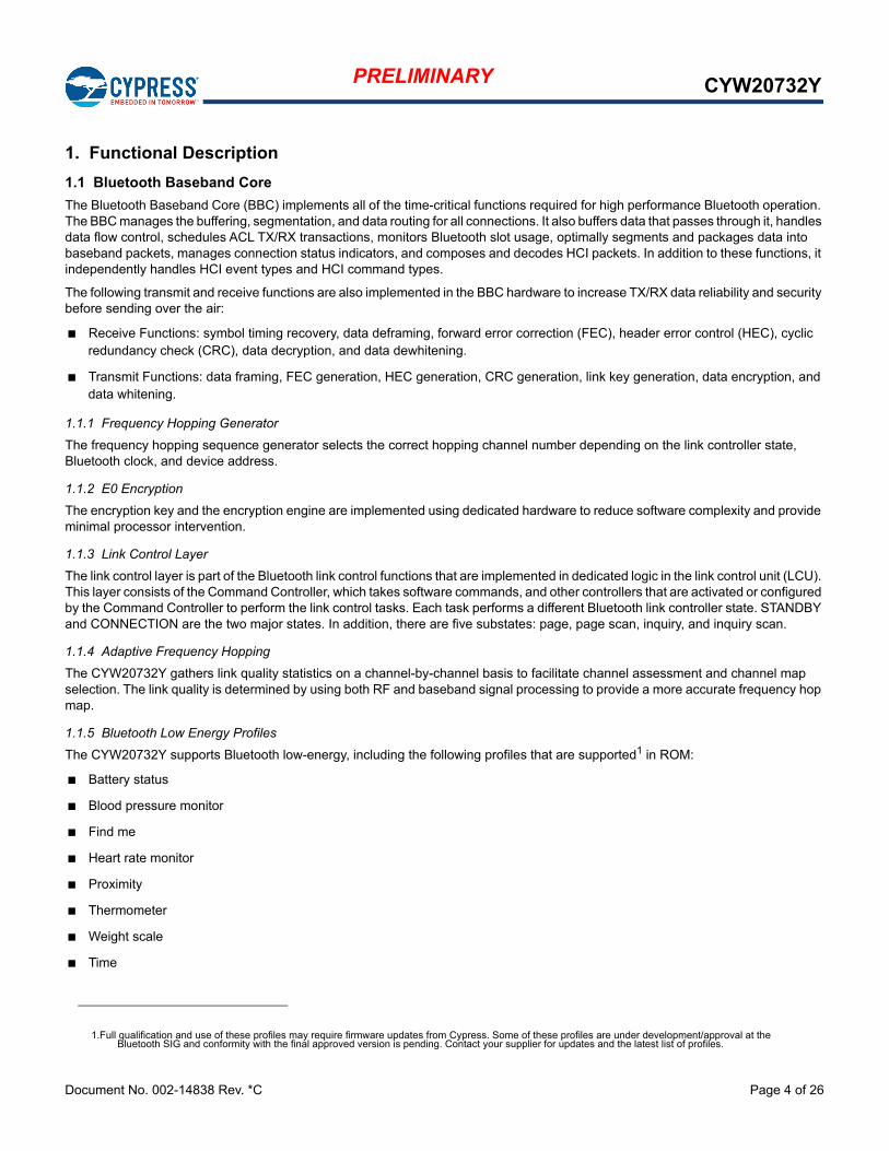
Figure 1. Functional Block Diagram
Introduction
This data sheet provides a description of the major blocks, interfaces, pin assignments, and specifications of the CYW20732Y single-chip Bluetooth low energy (BLE) SoC. This is a required document for designers responsible for adding the CYW20732Y BLE SoC to wireless input device applications including heart-rate monitors, blood-pressure monitors, proximity sensors, temperature sensors, and battery monitors.
Cypress Part Numbering Scheme
Cypress is converting the acquired IoT part numbers from Cypress to the Cypress part numbering scheme. Due to this conversion, there is no change in form, fit, or function as a result of offering the device with Cypress part number marking. The table provides Cypress ordering part number that matches an existing IoT part number.
Table 1. Mapping Table for Part Number between Broadcom and Cypress
Acronyms and Abbreviations
In most cases, acronyms and abbreviations are defined upon first use. For a more complete list of acronyms and other terms used in Cypress documents, go to: http://www.cypress.com/glossary.
IoT Resources
Cypress provides a wealth of data at http://www.cypress.com/internet-things-iot to help you to select the right IoT device for your design, and quickly and effectively integrate the device into your design. Cypress provides customer access to a wide range of information, including technical documentation, schematic diagrams, product bill of materials, PCB layout information, and software updates. Customers can acquire technical documentation and software from the Cypress Support Community website (https://community.cypress.com/).
CYW20732Y
with ARM Cortex M3
microprocessor core
BT_RF
XTAL2.4 MHz
VBAT VDDC VDBL
UART interface
I2C
GPIOs
PCM
Flash
1 Mbit I2C
VDBL_EE
Broadcom Part Number Cypress Part Number
BCM20732Y CYW20732Y
BCM20732YB3ISLGH (T) CYW20732YB3ISLGH (T)

Document No. 002-14838 Rev. *C Page 3 of 26
PRELIMINARY CYW20732Y
Contents1. Functional Description ..................................... 4
1.1 Bluetooth Baseband Core ................................... 41.1.1 Frequency Hopping Generator ................ 41.1.2 E0 Encryption .......................................... 41.1.3 Link Control Layer ................................... 41.1.4 Adaptive Frequency Hopping .................. 41.1.5 Bluetooth Low Energy Profiles ................ 41.1.6 Test Mode Support .................................. 5
1.2 Infrared Modulator ............................................... 5
1.3 Infrared Learning ................................................. 5
1.4 Serial Peripheral Interface ................................... 5
1.5 Microprocessor Unit ............................................ 61.5.1 EEPROM Interface .................................. 61.5.2 Serial Flash Interface ............................... 6
2. Pin Assignments............................................... 7
2.1 Pin Descriptions .................................................. 7
2.2 Pin Definition ....................................................... 8
3. Electrical Specifications................................... 9
3.1 Absolute Maximum Ratings ................................ 9
3.2 Recommended Operating Conditions ................. 93.2.1 Temperature and Humidity ...................... 9
3.2.2 Voltage .................................................... 93.2.3 Current Consumption .............................. 9
4. RF Specifications............................................ 10
4.1 RF Performance ................................................ 10
4.2 RF Transmitter Specifications ............................10
5. Timing Specifications..................................... 11
5.1 External Reset ....................................................11
5.2 Timing and AC Characteristics ...........................125.2.1 SPI Timing ..............................................125.2.2 BSC Interface Timing .............................135.2.3 UART Timing ..........................................14
5.2.4 Crystal Oscillator ....................................14
6. Mechanical ...................................................... 15
6.1 Dimensions ........................................................15
6.2 Recommended Footprint ....................................16
6.3 Recommended Stencil .......................................17
6.4 Recommended Reflow Profile ............................18
7. Packaging and Storage .................................. 19
7.1 Package Dimensioning ......................................19
7.2 Laser Mark .........................................................20
7.3 Pin 1 Location in the Tape/Reel .........................20
7.4 Moisture Sensitive Level (MSL) .........................21
7.5 SiP Module Tray .................................................22
7.6 Product Qualification Report ..............................23
8. Ordering Information...................................... 24
Document History Page................................................. 25
Sales, Solutions, and Legal Information ...................... 26
Document No. 002-14838 Rev. *C Page 4 of 26
PRELIMINARY CYW20732Y
1. Functional Description
1.1 Bluetooth Baseband Core
The Bluetooth Baseband Core (BBC) implements all of the time-critical functions required for high performance Bluetooth operation. The BBC manages the buffering, segmentation, and data routing for all connections. It also buffers data that passes through it, handles data flow control, schedules ACL TX/RX transactions, monitors Bluetooth slot usage, optimally segments and packages data into baseband packets, manages connection status indicators, and composes and decodes HCI packets. In addition to these functions, it independently handles HCI event types and HCI command types.
The following transmit and receive functions are also implemented in the BBC hardware to increase TX/RX data reliability and security before sending over the air:
Receive Functions: symbol timing recovery, data deframing, forward error correction (FEC), header error control (HEC), cyclic redundancy check (CRC), data decryption, and data dewhitening.
Transmit Functions: data framing, FEC generation, HEC generation, CRC generation, link key generation, data encryption, and data whitening.
1.1.1 Frequency Hopping Generator
The frequency hopping sequence generator selects the correct hopping channel number depending on the link controller state, Bluetooth clock, and device address.
1.1.2 E0 Encryption
The encryption key and the encryption engine are implemented using dedicated hardware to reduce software complexity and provide minimal processor intervention.
1.1.3 Link Control Layer
The link control layer is part of the Bluetooth link control functions that are implemented in dedicated logic in the link control unit (LCU). This layer consists of the Command Controller, which takes software commands, and other controllers that are activated or configured by the Command Controller to perform the link control tasks. Each task performs a different Bluetooth link controller state. STANDBY and CONNECTION are the two major states. In addition, there are five substates: page, page scan, inquiry, and inquiry scan.
1.1.4 Adaptive Frequency Hopping
The CYW20732Y gathers link quality statistics on a channel-by-channel basis to facilitate channel assessment and channel map selection. The link quality is determined by using both RF and baseband signal processing to provide a more accurate frequency hop map.
1.1.5 Bluetooth Low Energy Profiles
The CYW20732Y supports Bluetooth low-energy, including the following profiles that are supported1 in ROM:
Battery status
Blood pressure monitor
Find me
Heart rate monitor
Proximity
Thermometer
Weight scale
Time
1.Full qualification and use of these profiles may require firmware updates from Cypress. Some of these profiles are under development/approval at the Bluetooth SIG and conformity with the final approved version is pending. Contact your supplier for updates and the latest list of profiles.
Document No. 002-14838 Rev. *C Page 5 of 26
PRELIMINARY CYW20732Y
The following additional profiles can be supported1 from RAM:
Blood glucose monitor
Temperature alarm
Location
Custom profile
1.1.6 Test Mode Support
The CYW20732Y fully supports Bluetooth Test mode, as described in the Bluetooth low energy specification.
1.2 Infrared Modulator
The CYW20732Y includes hardware support for infrared TX. The hardware can transmit both modulated and unmodulated waveforms. For modulated waveforms, hardware inserts the desired carrier frequency into all IR transmissions. IR TX can be sourced from firmware-supplied descriptors, a programmable bit, or the peripheral UART transmitter.
If descriptors are used, they include IR on/off state and the duration between 1 and 32,767 µsec. The CYW20732Y IR TX firmware driver inserts this information in a hardware FIFO and makes sure that all descriptors are played out without a glitch due to underrun.
1.3 Infrared Learning
The CYW20732Y includes hardware support for infrared learning. The hardware can detect both modulated and unmodulated signals. For modulated signals, the CYW20732Y can detect carrier frequencies between 10 kHz– 500 kHz and the duration that the signal is present or absent. The CYW20732Y firmware driver supports further analysis and compression of learned signal. The learned signal can then be played back through the CYW20732Y IR TX subsystem.
1.4 Serial Peripheral Interface
The CYW20732Y has two independent SPI interfaces. One is a master-only interface and the other can be either a master or a slave. Each interface has a 16-byte transmit buffer and a 16-byte receive buffer. To support more flexibility for user applications, the CYW20732Y has optional I/O ports that can be configured individually and separately for each functional pin.

Document No. 002-14838 Rev. *C Page 6 of 26
PRELIMINARY CYW20732Y
1.5 Microprocessor Unit
The CYW20732Y microprocessor unit (µPU) executes software from the link control (LC) layer up to the application layer components. The microprocessor is based on an ARM Cortex-M3, 32-bit RISC processor with embedded ICE-RT debug and JTAG interface units. The µPU has 320 KB of ROM for program storage and boot-up, 60 KB of RAM for scratch-pad data, and patch RAM code. The SoC has a total storage of 380 KB, including RAM and ROM.
The internal boot ROM provides power-on reset flexibility, which enables the same device to be used in different HID applications with an external serial EEPROM or with an external serial flash memory. At power-up, the lowest layer of the protocol stack is executed from the internal ROM memory.
External patches may be applied to the ROM-based firmware to provide flexibility for bug fixes and feature additions. The device can also support the integration of user applications.
1.5.1 EEPROM Interface
The CYW20732Y provides a Broadcom Serial Control (BSC) master interface. BSC is programmed by the CPU to generate four types of bus transfers: read-only, write-only, combined read/write, and combined write/read. BSC supports both low-speed and fast mode devices. BSC is compatible with an NXP I2C slave device, except that master arbitration (multiple I2C masters contending for the bus) is not supported.
The EEPROM can contain customer application configuration information including application code, configuration data, patches, pairing information, BD_ADDR, baud rate, SDP service record, and file system information used for code.
Native support for the Microchip 24LC128, Microchip 24AA128, and the STMicroelectronics M24128-BR is included.
1.5.2 Serial Flash Interface
The CYW20732Y includes an SPI master controller that can be used to access serial flash memory. The SPI master contains an AHB slave interface, transmit and receive FIFOs, and the SPI core PHY logic.
Devices natively supported include the following:
Atmel® AT25BCM512B
MXIC MX25V512ZUI-20G
Document No. 002-14838 Rev. *C Page 7 of 26
PRELIMINARY CYW20732Y
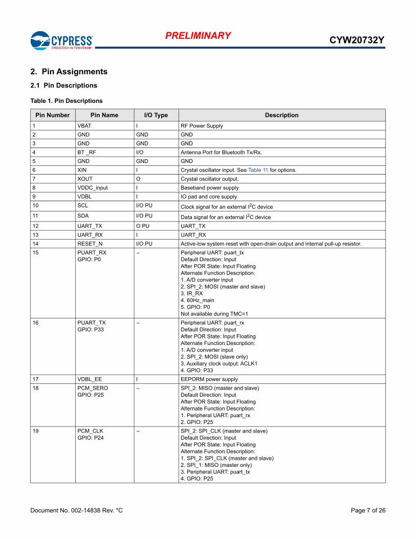
2. Pin Assignments
2.1 Pin Descriptions
Table 1. Pin Descriptions
Pin Number Pin Name I/O Type Description
1 VBAT I RF Power Supply
2 GND GND GND
3 GND GND GND
4 BT _RF I/O Antenna Port for Bluetooth Tx/Rx.
5 GND GND GND
6 XIN I Crystal oscillator input. See Table 11 for options.
7 XOUT O Crystal oscillator output.
8 VDDC_input I Baseband power supply
9 VDBL I IO pad and core supply
10 SCL I/O PU Clock signal for an external I2C device
11 SDA I/O PU Data signal for an external I2C device
12 UART_TX O PU UART_TX
13 UART_RX I UART_RX
14 RESET_N I/O PU Active-low system reset with open-drain output and internal pull-up resistor.
15 PUART_RXGPIO: P0
– Peripheral UART: puart_txDefault Direction: InputAfter POR State: Input FloatingAlternate Function Description:1. A/D converter input2. SPI_2: MOSI (master and slave)3. IR_RX4. 60Hz_main5. GPIO: P0Not available during TMC=1
16 PUART_TXGPIO: P33
– Peripheral UART: puart_rxDefault Direction: InputAfter POR State: Input FloatingAlternate Function Description:1. A/D converter input 2. SPI_2: MOSI (slave only)3. Auxiliary clock output: ACLK14. GPIO: P33
17 VDBL_EE I EEPORM power supply
18 PCM_SEROGPIO: P25
– SPI_2: MISO (master and slave)Default Direction: InputAfter POR State: Input FloatingAlternate Function Description:1. Peripheral UART: puart_rx2. GPIO: P25
19 PCM_CLKGPIO: P24
– SPI_2: SPI_CLK (master and slave)Default Direction: InputAfter POR State: Input FloatingAlternate Function Description:1. SPI_2: SPI_CLK (master and slave)2. SPI_1: MISO (master only)3. Peripheral UART: puart_tx4. GPIO: P25
Document No. 002-14838 Rev. *C Page 8 of 26
PRELIMINARY CYW20732Y
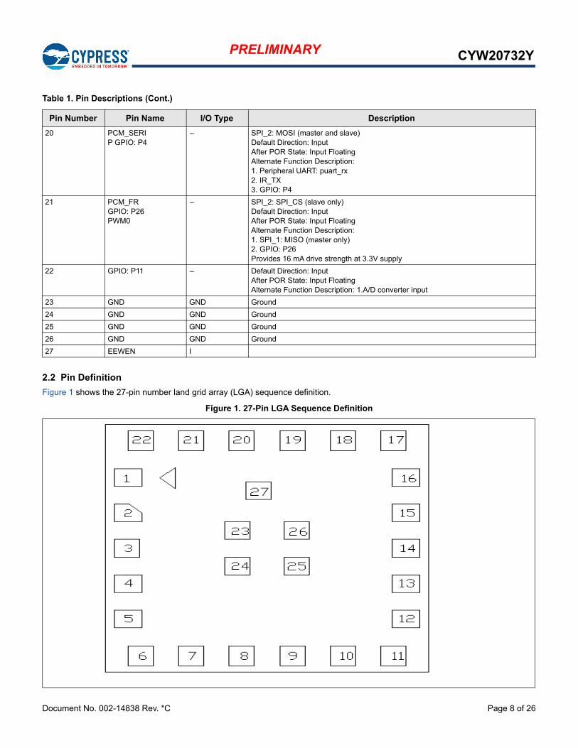
2.2 Pin Definition
Figure 1 shows the 27-pin number land grid array (LGA) sequence definition.
Figure 1. 27-Pin LGA Sequence Definition
20 PCM_SERIP GPIO: P4
– SPI_2: MOSI (master and slave)Default Direction: InputAfter POR State: Input FloatingAlternate Function Description:1. Peripheral UART: puart_rx2. IR_TX3. GPIO: P4
21 PCM_FRGPIO: P26PWM0
– SPI_2: SPI_CS (slave only)Default Direction: InputAfter POR State: Input FloatingAlternate Function Description: 1. SPI_1: MISO (master only) 2. GPIO: P26Provides 16 mA drive strength at 3.3V supply
22 GPIO: P11 – Default Direction: InputAfter POR State: Input FloatingAlternate Function Description: 1.A/D converter input
23 GND GND Ground
24 GND GND Ground
25 GND GND Ground
26 GND GND Ground
27 EEWEN I
Table 1. Pin Descriptions (Cont.)
Pin Number Pin Name I/O Type Description

Document No. 002-14838 Rev. *C Page 9 of 26
PRELIMINARY CYW20732Y
3. Electrical Specifications
3.1 Absolute Maximum Ratings
3.2 Recommended Operating Conditions
3.2.1 Temperature and Humidity
The CYW20732Y module must withstand the operational requirements shown in Table 3.
3.2.2 Voltage
The power supply for the CYW20732Y module is provided by the host via the power pins.
3.2.3 Current Consumption
The current consumption ratings will be based on an operating temperature condition of 25°C.
Table 2. Absolute Maximum Ratings
Requirement Power Min Max
Storage Temperature – –40° C 125°C
Voltage ripple – Max. Values not exceeding Operating voltage (+/- 2%)
Power Supply Absolute Maximum Ratings VBAT - 1.4V
Power Supply Absolute Maximum Ratings VDDC_Input - 1.4V
Power Supply Absolute Maximum Ratings VDBL - 3.8V
Power Supply Absolute Maximum Ratings VDBL_EE - 3.8V
Table 3. Temperature and Humidity
Condition Rating Description
Operating Temperature –30°C to 85°C –
Humidity range Maximum 95% Non condensing, relative humidity
Table 4. Recommended Voltages
Symbol Parameter Min Typ Max Unit
VBAT – 1.14 1.2 1.26 V
VDDC_Input – 1.14 1.2 1.26 –
VDBL – 1.62 – 3.63 –
VDBL_EE – 1.70 – 3.63 V
Table 5. Current Consumption
Item Condition Min Nom Max Unit
Receive Receiver and baseband are both operating at 100% 19.0 – 20.8 mA
Transmit Transmitter and baseband are both operating at 100% 19.0 – 19.7 mA
Sleep – 1.2 – 1.5 μA

Document No. 002-14838 Rev. *C Page 10 of 26
PRELIMINARY CYW20732Y
4. RF Specifications
4.1 RF Performance
4.2 RF Transmitter Specifications
Table 6. RF Performance
Parameter Mode and Conditions Min. Typ. Max. Unit
Receiver Section
Frequency range 2402 – 2480 MHz
RX sensitivity (standard) Packets: 200, Payload: PRBS 9, Length: 37 Bytes, Dirty Transmitter: off. PER: 30.8%
–92 – – dBm
Maximum input –10 – – dBm
Table 7. RF Transmitter Specifications
Parameter Mode and Conditions Min. Typ. Max. Unit
Transmitter Section
Frequency range – 2402 – 2480 MHz
Output power adjustment range – -20 – 4 dBm
Output power – – 3 – dBm
Output power variation – – 2 – dB
LO Performance
Initial carrier frequency tolerance - – – ±150 KHz
Frequency Drift
Frequency drift – – – ±50 kHz
Drift rate – – – 20 kHz/50 µs
Frequency Deviation
Average deviation in payload(sequence used is 00001111)
– 225 – 275 kHz
Average deviation in payload(sequence used is 10101010)
– 185 – – kHz
Channel spacing – – 2 – MHz
Note: The RF transmitter specification compliance is to the BT 4.0 standard with conductive measurements.

Document No. 002-14838 Rev. *C Page 11 of 26
PRELIMINARY CYW20732Y
5. Timing Specifications
5.1 External Reset
Figure 2. External Reset Timing
Document No. 002-14838 Rev. *C Page 12 of 26
PRELIMINARY CYW20732Y
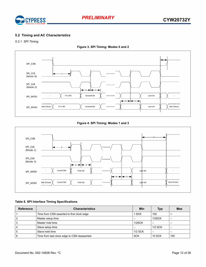
5.2 Timing and AC Characteristics
5.2.1 SPI Timing
Figure 3. SPI Timing: Modes 0 and 2
Figure 4. SPI Timing: Modes 1 and 3
Table 8. SPI Interface Timing Specifications
Reference Characteristics Min Typ Max
1 Time from CSN asserted to first clock edge 1 SCK 100 ∞
2 Master setup time – 1/2SCK –
3 Master hold time 1/2SCK – –
4 Slave setup time – 1/2 SCK –
5 Slave hold time 1/2 SCK – –
6 Time from last clock edge to CSN deasserted SCK 10 SCK 100

Document No. 002-14838 Rev. *C Page 13 of 26
PRELIMINARY CYW20732Y
5.2.2 BSC Interface Timing
Figure 5. BSC Interface Timing
Table 9. BSC Interface Timing Specifications
Reference Characteristics Min Max Unit
1 Clock frequencies – 100 KHz
– 400 KHz
– 800 KHz
– 1000 KHz
2 START condition setup time 650 – ns
3 START condition hold time 280 – ns
4 Clock low time 650 – ns
5 Clock high time 280 – ns
6 Data input hold time 0 – ns
7 Data input setup time 100 – ns
8 STOP condition setup time 280 – ns
9 Output valid from clock – 400 ns
10 Bus free time 650 – ns

Document No. 002-14838 Rev. *C Page 14 of 26
PRELIMINARY CYW20732Y
5.2.3 UART Timing
Figure 6. UART Timing
5.2.4 Crystal Oscillator
The CYW20732Y is set with a crystal frequency of 24 MHz. The crystal oscillator requires a crystal with an accuracy of ±20 ppm as defined by the Bluetooth specification. Two external load capacitors in the range of 5 pF to 30 pF are required to function with the crystal oscillator. The selection of the load capacitors is crystal dependent. Table 11 shows the recommended crystal specification.
Table 10. UART Timing Specifications
Reference Characteristics Min Max Unit
1 Delay time, UART_CTS_N low to UART_TXD valid – 24 Baudout cycles
2 Setup time, UART_CTS_N high before midpoint of stop bit – 10 ns
3 Delay time, midpoint of stop bit to UART_RTS_N high – 2 Baudout cycles
Table 11. Crystal Oscillator
Parameter Symbol Conditions Min Typ Max Unit
Frequency – – – 24.000 – MHz
Oscillation Mode – Fundamental – – –
Frequency tolerance @25°C – – ±10 – ppm
Tolerance stability over temp @-20°C to +85°C – – ±10 – ppm
Equivalent series resistance – – – – 50 Ω
Load Capacitance – – – 12 – pF
Document No. 002-14838 Rev. *C Page 15 of 26
PRELIMINARY CYW20732Y
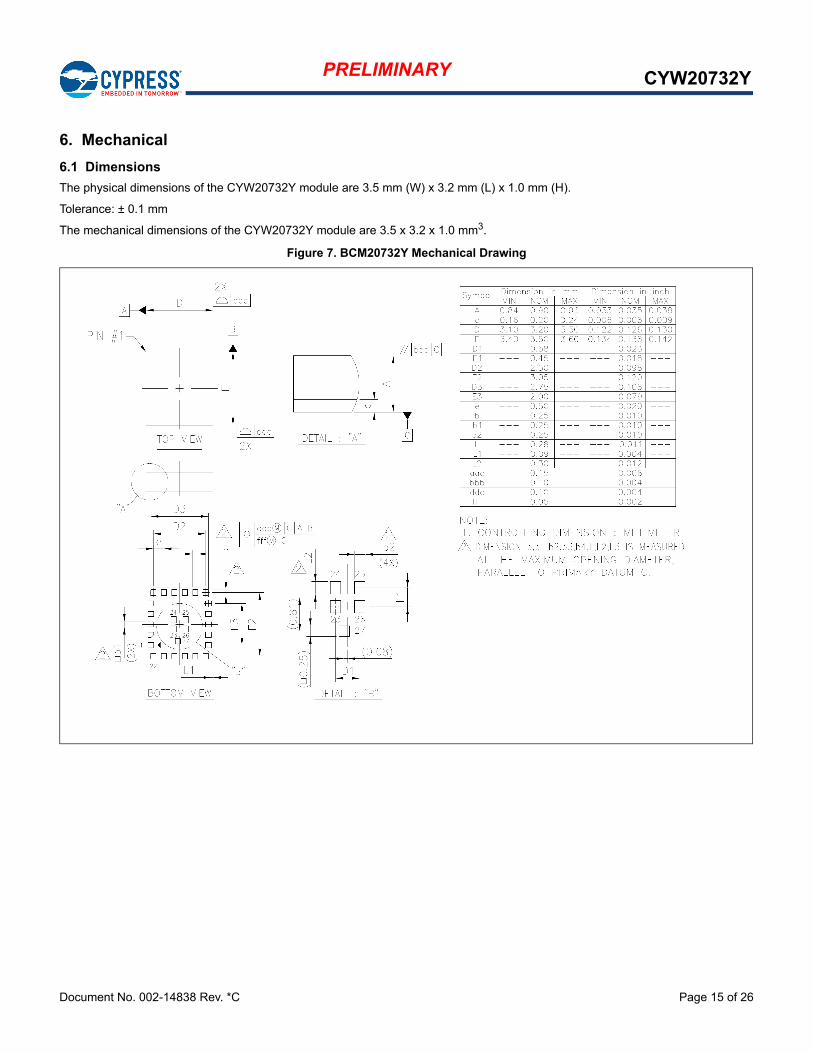
6. Mechanical
6.1 Dimensions
The physical dimensions of the CYW20732Y module are 3.5 mm (W) x 3.2 mm (L) x 1.0 mm (H).
Tolerance: ± 0.1 mm
The mechanical dimensions of the CYW20732Y module are 3.5 x 3.2 x 1.0 mm3.
Figure 7. BCM20732Y Mechanical Drawing

Document No. 002-14838 Rev. *C Page 16 of 26
PRELIMINARY CYW20732Y
6.2 Recommended Footprint
The CYW20732Y module dimension measurement is in mm.
Figure 8. BCM20732Y Recommended Footprint
Notes:
1. Use the NCMD standard to design the main board footprint.
2. There are three types of pads in the module:
a. Type A: pad size: 0.275 x 0.25 mm with a solder mask opening of 0.375 x 0.35 mm.
b. Type B: pad size: 0.3 x 0.25 mm with a solder mask opening of 0.4 x 0.35 mm.
c. Type C: pad size: 0.25 x 0.25 mm with a solder mask opening of 0.35 x 0.35 mm.
Document No. 002-14838 Rev. *C Page 17 of 26
PRELIMINARY CYW20732Y
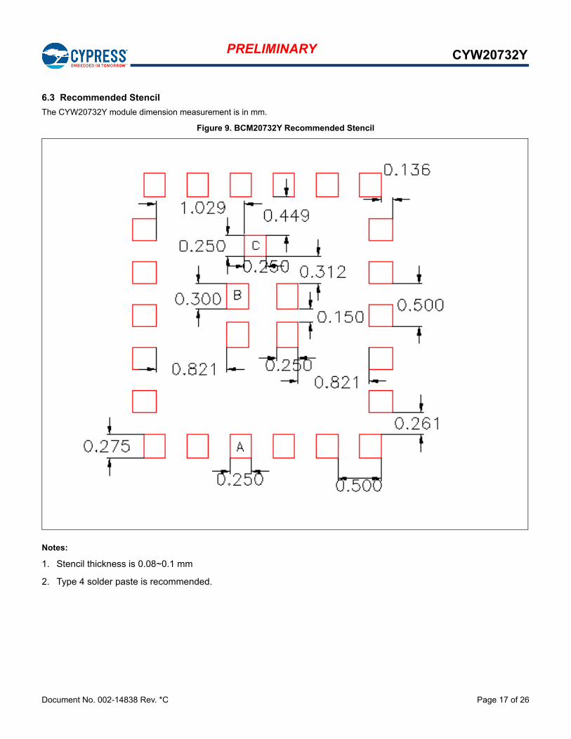
6.3 Recommended Stencil
The CYW20732Y module dimension measurement is in mm.
Figure 9. BCM20732Y Recommended Stencil
Notes:
1. Stencil thickness is 0.08~0.1 mm
2. Type 4 solder paste is recommended.

Document No. 002-14838 Rev. *C Page 18 of 26
PRELIMINARY CYW20732Y
6.4 Recommended Reflow Profile
Figure 10. Recommended Reflow Profile
2000C
2170C
2450C
1500C
Pre- heating Soldering
90~120 sec 60~90 sec
Tem
per
atu
re
Time

Document No. 002-14838 Rev. *C Page 19 of 26
PRELIMINARY CYW20732Y
7. Packaging and Storage
7.1 Package Dimensioning
Figure 11. Package Dimensioning
Document No. 002-14838 Rev. *C Page 20 of 26
PRELIMINARY CYW20732Y
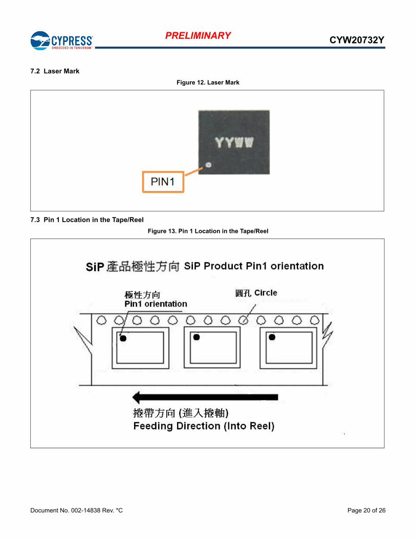
7.2 Laser Mark
Figure 12. Laser Mark
7.3 Pin 1 Location in the Tape/Reel
Figure 13. Pin 1 Location in the Tape/Reel
Document No. 002-14838 Rev. *C Page 21 of 26
PRELIMINARY CYW20732Y
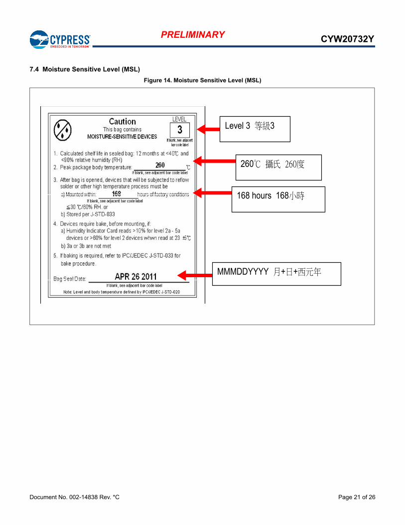
7.4 Moisture Sensitive Level (MSL)
Figure 14. Moisture Sensitive Level (MSL)
Level 3 3
260
168 hours 168
MMMDDYYYY + +

Document No. 002-14838 Rev. *C Page 22 of 26
PRELIMINARY CYW20732Y
7.5 SiP Module Tray
The CYW20732Y SiP module tray is shown in Figure 15. The tray dimensions are 3.2 mm x 3.5 mm.
Figure 15. SiP Module Tray
Document No. 002-14838 Rev. *C Page 23 of 26
PRELIMINARY CYW20732Y
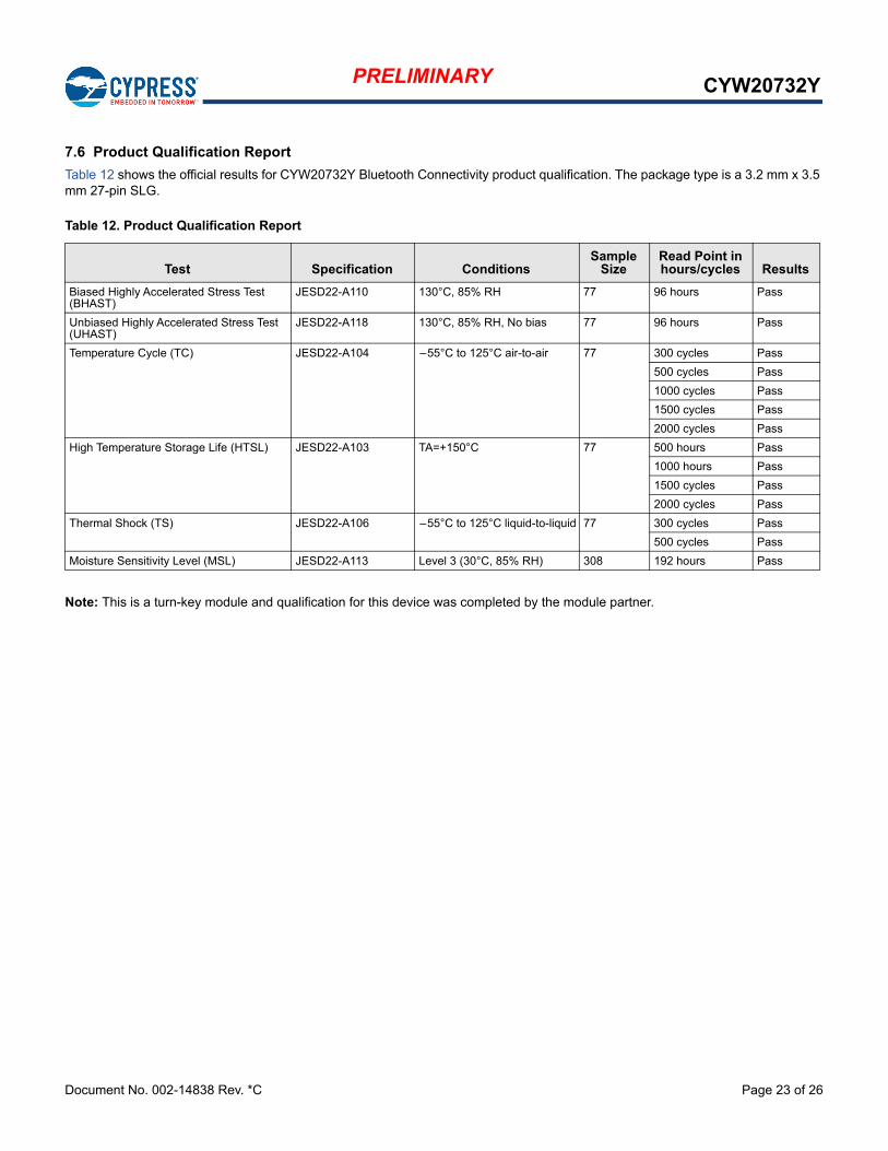
7.6 Product Qualification Report
Table 12 shows the official results for CYW20732Y Bluetooth Connectivity product qualification. The package type is a 3.2 mm x 3.5 mm 27-pin SLG.
Note: This is a turn-key module and qualification for this device was completed by the module partner.
Table 12. Product Qualification Report
Test Specification ConditionsSample
SizeRead Point in hours/cycles Results
Biased Highly Accelerated Stress Test (BHAST)
JESD22-A110 130°C, 85% RH 77 96 hours Pass
Unbiased Highly Accelerated Stress Test (UHAST)
JESD22-A118 130°C, 85% RH, No bias 77 96 hours Pass
Temperature Cycle (TC) JESD22-A104 –55°C to 125°C air-to-air 77 300 cycles Pass
500 cycles Pass
1000 cycles Pass
1500 cycles Pass
2000 cycles Pass
High Temperature Storage Life (HTSL) JESD22-A103 TA=+150°C 77 500 hours Pass
1000 hours Pass
1500 cycles Pass
2000 cycles Pass
Thermal Shock (TS) JESD22-A106 –55°C to 125°C liquid-to-liquid 77 300 cycles Pass
500 cycles Pass
Moisture Sensitivity Level (MSL) JESD22-A113 Level 3 (30°C, 85% RH) 308 192 hours Pass

Document No. 002-14838 Rev. *C Page 24 of 26
PRELIMINARY CYW20732Y
8. Ordering Information
Table 13. Ordering Information
Part Number Package DescriptionAmbient Operating
Temperature
CYW20732YB3ISLGH (T) Note: T represents Tape and Reel.
27-pin 27-LGA (3.5 mm × 3.2 mm x 1.0 mm) package
Bluetooth Low Energy SiP Module –55°C to +125°C°

Document No. 002-14838 Rev. *C Page 25 of 26
PRELIMINARY CYW20732Y
Document History Page
Document Title: CYW20732Y Bluetooth Low Energy SiP Module Document Number: 002-14838
Revision ECN Orig. of Change
Submission Date Description of Change
** - - 06/10/2015 20732Y-DS100-R
Initial release
*A - - 03/07/2016 20732Y-DS101-R
Updated:• “Features” on cover page.• Table5. “Current Consumption"
Added:• “Features” on cover page.• “SiP Module Tray”.• “Product Qualification Report”.• Section 8. “Ordering Information”
*B 5484081 UTSAV 10/20/2016Added Cypress Part Numbering Scheme and Mapping Table on Page 1.
Updated to Cypress template.
*C 5962423 AESATMP9 11/09/2017 Updated logo and copyright.

Document No. 002-14838 Rev. *C Revised November 9, 2017 Page 26 of 26
© Cypress Semiconductor Corporation, 2015-2017. This document is the property of Cypress Semiconductor Corporation and its subsidiaries, including Spansion LLC ("Cypress"). This document,including any software or firmware included or referenced in this document ("Software"), is owned by Cypress under the intellectual property laws and treaties of the United States and other countriesworldwide. Cypress reserves all rights under such laws and treaties and does not, except as specifically stated in this paragraph, grant any license under its patents, copyrights, trademarks, or otherintellectual property rights. If the Software is not accompanied by a license agreement and you do not otherwise have a written agreement with Cypress governing the use of the Software, then Cypresshereby grants you a personal, non-exclusive, nontransferable license (without the right to sublicense) (1) under its copyright rights in the Software (a) for Software provided in source code form, tomodify and reproduce the Software solely for use with Cypress hardware products, only internally within your organization, and (b) to distribute the Software in binary code form externally to end users(either directly or indirectly through resellers and distributors), solely for use on Cypress hardware product units, and (2) under those claims of Cypress's patents that are infringed by the Software (asprovided by Cypress, unmodified) to make, use, distribute, and import the Software solely for use with Cypress hardware products. Any other use, reproduction, modification, translation, or compilationof the Software is prohibited.
TO THE EXTENT PERMITTED BY APPLICABLE LAW, CYPRESS MAKES NO WARRANTY OF ANY KIND, EXPRESS OR IMPLIED, WITH REGARD TO THIS DOCUMENT OR ANY SOFTWAREOR ACCOMPANYING HARDWARE, INCLUDING, BUT NOT LIMITED TO, THE IMPLIED WARRANTIES OF MERCHANTABILITY AND FITNESS FOR A PARTICULAR PURPOSE. To the extentpermitted by applicable law, Cypress reserves the right to make changes to this document without further notice. Cypress does not assume any liability arising out of the application or use of anyproduct or circuit described in this document. Any information provided in this document, including any sample design information or programming code, is provided only for reference purposes. It isthe responsibility of the user of this document to properly design, program, and test the functionality and safety of any application made of this information and any resulting product. Cypress productsare not designed, intended, or authorized for use as critical components in systems designed or intended for the operation of weapons, weapons systems, nuclear installations, life-support devices orsystems, other medical devices or systems (including resuscitation equipment and surgical implants), pollution control or hazardous substances management, or other uses where the failure of thedevice or system could cause personal injury, death, or property damage ("Unintended Uses"). A critical component is any component of a device or system whose failure to perform can be reasonablyexpected to cause the failure of the device or system, or to affect its safety or effectiveness. Cypress is not liable, in whole or in part, and you shall and hereby do release Cypress from any claim,damage, or other liability arising from or related to all Unintended Uses of Cypress products. You shall indemnify and hold Cypress harmless from and against all claims, costs, damages, and otherliabilities, including claims for personal injury or death, arising from or related to any Unintended Uses of Cypress products.
Cypress, the Cypress logo, Spansion, the Spansion logo, and combinations thereof, WICED, PSoC, CapSense, EZ-USB, F-RAM, and Traveo are trademarks or registered trademarks of Cypress inthe United States and other countries. For a more complete list of Cypress trademarks, visit cypress.com. Other names and brands may be claimed as property of their respective owners.
PRELIMINARY CYW20732Y
Sales, Solutions, and Legal Information
Worldwide Sales and Design Support
Cypress maintains a worldwide network of offices, solution centers, manufacturer’s representatives, and distributors. To find the officeclosest to you, visit us at Cypress Locations.
Products
ARM® Cortex® Microcontrollers cypress.com/arm
Automotive cypress.com/automotive
Clocks & Buffers cypress.com/clocks
Interface cypress.com/interface
Internet of Things cypress.com/iot
Memory cypress.com/memory
Microcontrollers cypress.com/mcu
PSoC cypress.com/psoc
Power Management ICs cypress.com/pmic
Touch Sensing cypress.com/touch
USB Controllers cypress.com/usb
Wireless Connectivity cypress.com/wireless
PSoC® Solutions
PSoC 1 | PSoC 3 | PSoC 4 | PSoC 5LP | PSoC 6
Cypress Developer Community
Forums | WICED IoT Forums | Projects | Video | Blogs |Training | Components
Technical Support
cypress.com/support
Mouser Electronics
Authorized Distributor
Click to View Pricing, Inventory, Delivery & Lifecycle Information: Cypress Semiconductor:
BCM20732Y BCM20732YT CYW20732YT CYW20732Y