Embed Size (px)
Citation preview

CW014-Channel Low-Phase-Noise Low-Power Continuous Wave Transmitter
Features
• Low Phase Noise
• 100V Open Drain N-channel
• High-speed D Flip-flop
• High-speed MOSFET Gate Driver
• Up to 200 MHz Clock Input
• VDD and VLL Undervoltage Lockout
Applications
• Diagnostic Medical Ultrasound
• Fluid Flow Measurement
General Description
The CW01 is a 4-channel low-phase-noise continuous wave transmitter IC. A high-speed D flip-flop is provided to allow the DIN frequency to be aligned to a high-frequency clock. The output N-channel is turned on when a logic high is clocked into the D flip-flop. Data are clocked-in during the low-to-high transition.
VD1, VD2, VD3 and VD4 are four individual input supply voltages for the N-channel output MOSFET gate drivers. High peak currents are drawn from these gate drives when the output MOSFETs are switching. To minimize jitter caused by voltage ripples, each channel has its own gate drive voltage pin—VD1, VD2, VD3 and VD4. A series ferrite bead and a decoupling capacitor are recommended on each VDX pin to minimize output jitter and channel-to-channel crosstalk.
Both VDD and VLL have undervoltage lockout to prevent spurious turn-on.
Package Type
See Table 2-1 for pin information.
24-lead QFN(Top view)
OE
VS
S
VD
1
VD
2
PG
ND
1
HVOUT
1
PGND2
HVOUT
2
VSS
HVOUT
3
PGND3
HVOUT
4
VL
L
VS
S
VD
4
VD
3
PG
ND
4
DIN1
DIN2
VDD
CLK
VSS
DIN3
DIN4
1
24
2017 Microchip Technology Inc. DS20005810A-page 1

CW01
Functional Block Diagram
VDD
VLL
OE
DIN
1
DIN
2
DIN
3
DIN
4
CLK
VSS
VLL
VLL
VLL
VLLVDD
VDD
VDD
VDD
VLL
UVLO
VDD
UVLO
DIN
1
Q1 CLK
DIN
2
Q1 CLK
DIN
3
Q1 CLK
DIN
4
Q1 CLK
VD1
HVOUT
1
PGND1
VD2
HVOUT
2
PGND2
VD3
HVOUT
3
PGND3
VD4
HVOUT
4
PGND4
SUB
DS20005810A-page 2 2017 Microchip Technology Inc.

CW01
Typical Application Circuit
HVOUT
1
PGND1
Translatorand Driver
VD1VLL
270μH
0.1μF
0.1μF
5.0V
2.5V
2.0 to5.0MHz
96MHz
VD1
VDD
OE
VLL
DIN
1
CLK
VSS
DIN
1
Q1 CLK
BAV99
Tx
PZT
8.0V
BAV23
(One of four channels)
2017 Microchip Technology Inc. DS20005810A-page 3

CW01
1.0 ELECTRICAL CHARACTERISTICS
Absolute Maximum Ratings†
Logic Supply, VLL ....................................................................................................................................... –0.3V to +6VLevel Translator Voltage, VDD ................................................................................................................... –0.5V to +6VGate Drive Voltage, VDX ............................................................................................................................ –0.5V to +6VHigh-voltage Output Drain Voltage, HVOUT ............................................................................................. –0.5 to +120VOperating Junction Temperature, TJ ................................................................................................... –40°C to +125°CStorage Temperature, TS ..................................................................................................................... –65°C to +150°CPower Dissipation (TA = 25°C):
† Notice: Stresses above those listed under “Absolute Maximum Ratings” may cause permanent damage to the device. This is a stress rating only, and functional operation of the device at those or any other conditions above those indicated in the operational sections of this specification is not intended. Exposure to maximum rating conditions for extended periods may affect device reliability.
24-lead QFN........................................................................................................................................................ 3W
DC ELECTRICAL CHARACTERISTICS Electrical Specifications: VDD = VDX = 5V, VLL = 2.5V, TJ = 25ºC unless otherwise specified.
Parameter Sym. Min. Typ. Max. Unit Conditions
High-voltage Output HVOUT 0 — 100 V
VDD Voltage Range VDD 4.5 5 5.5 V
VDD Rise Time tVDD–ON 50 — — µs
VLL Voltage Range VLL 1.65 2.5 5.5 V
VLL Rise Time tVLL–ON 50 — — µs
Logic Input Voltage Range VDIN 0 — VLL V
Gate Drive Voltage VDX 4.5 5 5.5 V
VDX Rise Time tVDX–ON 50 — — µs
VDD Quiescent Current IDDQ — 63 100 µA
VDD Average Current IDD — 23.5 30 mAfCLK = 200 MHz, fOUT = 5 MHz, All four channels active
VLL Quiescent Current ILLQ — 8.1 20 µA
VLL Average Current ILL — 380 600 µAfCLK = 200 MHz, fOUT = 5 MHz, All four channels active
VDX Quiescent Current IDXQ — 0 1 µA
VDX Average Current IDX — 11.3 30 mAfCLK = 200 MHz, fOUT = 5 MHz, All four channels active
Input Logic High Voltage VIH 0.8 VLL — VLL V
Input Logic Low Voltage VIL 0 — 0.2 VLL V
Input Logic High Current IIH — — 1 µA
Input Logic High Current IIL –1 — — µA
Output On-resistance RON — 4.7 7 Ω IIN = 100 mA
Output Saturation Current ISAT — 0.8 — A VDD = HVOUT = 5V
High-voltage Output Leakage IHVleak — — 10 µA HVOUT = 100V
UVLO Trip Point for VLL UVLO_VLL — 1.5 — V
UVLO Trip Point for VDD UVLO_VDD — 4 — V
DS20005810A-page 4 2017 Microchip Technology Inc.

CW01
AC ELECTRICAL CHARACTERISTICSElectrical Specifications: VDD = VDX = 5V, VLL = 2.5V, TJ = 25ºC unless otherwise specified.
Parameter Sym. Min. Typ. Max. Unit Conditions
Clock Frequency fCLK 0 — 200 MHz
Clock Rise and Fall Times tr, tf — 0.5 5 ns
Set-up Time, DIN to CLK tSU 2 — — ns
Hold Time, DIN from CLK tH 1 — — ns
HVOUT Fall Time tHVf — 0.8 — nsLoad = 50Ω to 8V (See Timing Waveforms.)
HVOUT Rise Time tHVr — 3.3 — nsLoad = 50Ω to 8V (See Timing Waveforms.)
Delay Time from CLK to HVOUT from Low to High
tdLH — 5.1 — nsLoad = 50Ω to 8V (See Timing Waveforms.)
Delay Time from CLK to HVOUT from High to Low
tdHL — 2.6 — nsLoad = 50Ω to 8V (See Timing Waveforms.)
Delay Time Matching for tdLH ∆tdLHdelay — 0.5 1 ns
Delay Time Matching for tdHL ∆tdHLdelay — 0.5 1 ns
Output Enable Turn-on Time tOE(ON) — — 10 µs
Output Enable Turn-off Time tOE(OFF) — — 0.1 µs
Output Capacitance COUT— 8 — pF At 8V
— 4 — pF At 100V
Phase Noise NPhase — –171 –160 dBC/Hz
dB below carrier, CLK = 80 MHz, DIN = 2 MHz, Frequency offset = 1 kHz, Noise bandwidth = 140 Hz (See Figure 3-1 and Figure 3-2.)
TEMPERATURE SPECIFICATIONS
Parameter Sym. Min. Typ. Max. Unit Conditions
TEMPERATURE RANGE
Operating Junction Temperature TJ –40 — +125 °C
Storage Temperature TS –65 — +150 °C
PACKAGE THERMAL RESISTANCE
24-lead QFN JA — 26.9 — °C/W Note 1Note 1: Device is mounted on a 4-layer 3” by 4” board.
2017 Microchip Technology Inc. DS20005810A-page 5

CW01
Timing Waveforms
CLK
DIN
HVOUT tdLH
tHVr tHVf
tdHL
tH
tSU
50% 50%
90%90%
10% 10%
50% 50%
Typical Performance Curve
30
25
20
15
10
5
00 5 10 15 20 25
Data In Frequency (MHz)
I DD (
mA
)
fCLK = 200MHz
fCLK = 100MHz
fCLK = 50MHz
IDD vs. DIN Frequency
(Test conditions: VLL = 2.5V, VDD = 5V, VD1 = VD2 = VD3 = VD4 = 5V, no load)
DS20005810A-page 6 2017 Microchip Technology Inc.

CW01
2.0 PIN DESCRIPTION
Table 2-1 shows the description of pins in CW01. Refer to Package Type for the location of pins.
TABLE 2-1: PIN FUNCTION TABLE
Pin Number Pin Name Description
1 DIN1 D flip-flop logic input for HVOUT1. Logic high will turn on output N-channel.
2 DIN2 D flip-flop logic input for HVOUT2. Logic high will turn on output N-channel.
3 VDD Level translator supply. Should be at the same potential as VDX.
4 CLK Logic clock input
5 VSS Ground. Should be externally shorted to all PGND and VSS pins.
6 DIN3 D flip-flop logic input for HVOUT3. Logic high will turn on output N-channel.
7 DIN4 D flip-flop logic input for HVOUT4. Logic high will turn on output N-channel.
8 VLL Logic input supply voltage
9 VSS Ground. Should be externally shorted to all PGND and VSS pins.
10 VD4 Gate drive supply voltage for HVOUT4. Should be at the same potential as VDD.
11 VD3 Gate drive supply voltage for HVOUT3. Should be at the same potential as VDD.
12 PGND4Power ground for HVOUT4. Should be externally shorted to all PGND and VSS pins.
13 HVOUT4 Drain output for HVOUT4
14 PGND3Power ground for HVOUT3. Should be externally shorted to all PGND and VSS pins.
15 HVOUT3 Drain output for HVOUT3
16 VSS Ground. Should be externally shorted to all PGND and VSS pins.
17 HVOUT2 Drain output for HVOUT2
18 PGND2Power ground for HVOUT2. Should be externally shorted to all PGND and VSS pins.
19 HVOUT1 Drain output for HVOUT1
20 PGND1Power ground for HVOUT1. Should be externally shorted to all PGND and VSS pins.
21 VD2 Gate drive supply voltage for HVOUT2. Should be at the same potential as VDD.
22 VD1 Gate drive supply voltage for HVOUT1. Should be at the same potential as VDD.
23 VSS Ground. Should be externally shorted to all PGND and VSS pins.
24 OE Output enable logic input. Logic low will turn off all HVOUT.
Center Pad Should be externally shorted to all PGND and VSS pins.
2017 Microchip Technology Inc. DS20005810A-page 7

CW01
3.0 FUNCTIONAL DESCRIPTION
Figure 3-1 and Figure 3-2 illustrate the test circuits for CW01.
HVOUT
1
PGND1
HVOUT
Translatorand Driver
VD1VLL
0.1μF
8.0V
0.1μF
0.1μF5.0V
2.5V
DIN
CLK
VD1
VDD
OE
VLL
DIN
1
CLK
VSS
DIN
1
Q1 CLK
50Ω
(One of four channels)
FIGURE 3-1: AC Timing.
HVOUT
1
(One of four channels)
PGND1
HVOUT
Translatorand Driver
VD1VLL
0.1μF
50Ω
50Ω0.1μF
390μH
3.0V
0.1μF
0.1μF5.0V
2.5V
2.0MHz
80MHz
VD1
VDD
OE
VLL
DIN
1
CLK
VSS
DIN
1
Q1 CLK
FIGURE 3-2: Phase Noise.
DS20005810A-page 8 2017 Microchip Technology Inc.

CW01
4.0 PACKAGING INFORMATION
4.1 Package Marking Information
Legend: XX...X Product Code or Customer-specific informationY Year code (last digit of calendar year)YY Year code (last 2 digits of calendar year)WW Week code (week of January 1 is week ‘01’)NNN Alphanumeric traceability code Pb-free JEDEC® designator for Matte Tin (Sn)* This package is Pb-free. The Pb-free JEDEC designator ( )
can be found on the outer packaging for this package.
Note: In the event the full Microchip part number cannot be marked on one line, it will be carried over to the next line, thus limiting the number of available characters for product code or customer-specific information. Package may or not include the corporate logo.
3e
3e
24-lead QFN Example
XXXX e3XXXXXXXXXX
YYYYWWNNNWWNNN
K6K6 e3CW01CW01
17172552925529
2017 Microchip Technology Inc. DS20005810A-page 9
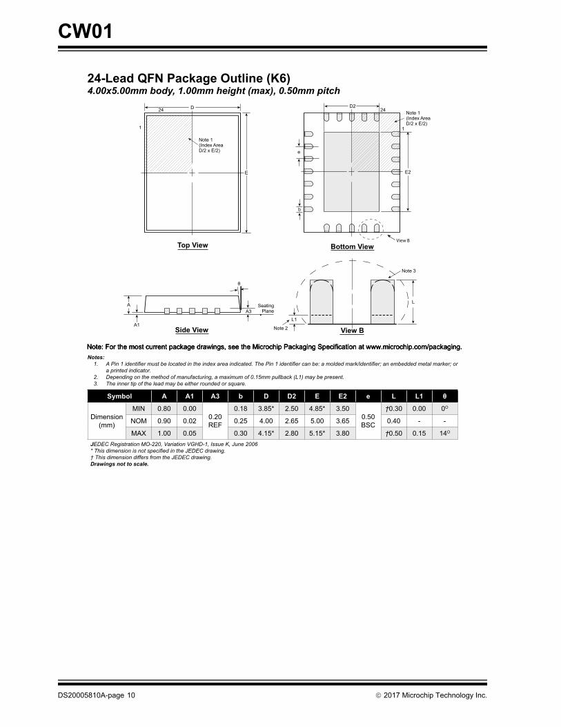
CW01
24-Lead QFN Package Outline (K6)4.00x5.00mm body, 1.00mm height (max), 0.50mm pitch
Symbol A A1 A3 b D D2 E E2 e L L1
Dimension(mm)
MIN 0.80 0.000.20REF
0.18 3.85* 2.50 4.85* 3.500.50BSC
†0.30 0.00 0O
NOM 0.90 0.02 0.25 4.00 2.65 5.00 3.65 0.40 - -
MAX 1.00 0.05 0.30 4.15* 2.80 5.15* 3.80 †0.50 0.15 14O
JEDEC Registration MO-220, Variation VGHD-1, Issue K, June 2006
Drawings not to scale.
SeatingPlane
Top View
Side View
Bottom View
A
A1
D
E
D2
b
E2
A3
L
L1
View B
View B
1
Note 3
Note 2
Note 1(Index AreaD/2 x E/2)
24
1
24
Note 1(Index AreaD/2 x E/2) e
Notes:1.
a printed indicator.2.3.
Note: For the most current package drawings, see the Microchip Packaging Specification at www.microchip.com/packaging.Note: For the most current package drawings, see the Microchip Packaging Specification at www.microchip.com/packaging.Note: For the most current package drawings, see the Microchip Packaging Specification at www.microchip.com/packaging.
DS20005810A-page 10 2017 Microchip Technology Inc.

2017 Microchip Technology Inc. DS20005810A-page 11
CW01
APPENDIX A: REVISION HISTORY
Revision A (July 2017)
• Converted Supertex Doc# DSFP-CW01 to Microchip DS20005810A
• Changed the package marking format
• Made minor text changes throughout the document

CW01
DS20005810A-page 12 2017 Microchip Technology Inc.
PRODUCT IDENTIFICATION SYSTEM
To order or obtain information, e.g., on pricing or delivery, contact your local Microchip representative or sales office.
Example:
a) CW01K6-G: Four-Channel Low-Phase-Noise Low-Power Continuous Wave Transmitter, 24-lead QFN, 3000/Reel
PART NO.
Device
Device: CW01 = Four-Channel Low-Phase-Noise Low-Power Continuous Wave Transmitter
Package: K6 = 24-lead QFN
Environmental: G = Lead (Pb)-free/RoHS-compliant Package
Media Type: (blank) = 3000/Reel for a K6 Package
XX
Package
- X - X
Environmental Media Type Options

Note the following details of the code protection feature on Microchip devices:
• Microchip products meet the specification contained in their particular Microchip Data Sheet.
• Microchip believes that its family of products is one of the most secure families of its kind on the market today, when used in the intended manner and under normal conditions.
• There are dishonest and possibly illegal methods used to breach the code protection feature. All of these methods, to our knowledge, require using the Microchip products in a manner outside the operating specifications contained in Microchip’s Data Sheets. Most likely, the person doing so is engaged in theft of intellectual property.
• Microchip is willing to work with the customer who is concerned about the integrity of their code.
• Neither Microchip nor any other semiconductor manufacturer can guarantee the security of their code. Code protection does not mean that we are guaranteeing the product as “unbreakable.”
Code protection is constantly evolving. We at Microchip are committed to continuously improving the code protection features of our products. Attempts to break Microchip’s code protection feature may be a violation of the Digital Millennium Copyright Act. If such acts allow unauthorized access to your software or other copyrighted work, you may have a right to sue for relief under that Act.
Information contained in this publication regarding device applications and the like is provided only for your convenience and may be superseded by updates. It is your responsibility to ensure that your application meets with your specifications. MICROCHIP MAKES NO REPRESENTATIONS OR WARRANTIES OF ANY KIND WHETHER EXPRESS OR IMPLIED, WRITTEN OR ORAL, STATUTORY OR OTHERWISE, RELATED TO THE INFORMATION, INCLUDING BUT NOT LIMITED TO ITS CONDITION, QUALITY, PERFORMANCE, MERCHANTABILITY OR FITNESS FOR PURPOSE. Microchip disclaims all liability arising from this information and its use. Use of Microchip devices in life support and/or safety applications is entirely at the buyer’s risk, and the buyer agrees to defend, indemnify and hold harmless Microchip from any and all damages, claims, suits, or expenses resulting from such use. No licenses are conveyed, implicitly or otherwise, under any Microchip intellectual property rights unless otherwise stated.
2017 Microchip Technology Inc.
Microchip received ISO/TS-16949:2009 certification for its worldwide headquarters, design and wafer fabrication facilities in Chandler and Tempe, Arizona; Gresham, Oregon and design centers in California and India. The Company’s quality system processes and procedures are for its PIC® MCUs and dsPIC® DSCs, KEELOQ® code hopping devices, Serial EEPROMs, microperipherals, nonvolatile memory and analog products. In addition, Microchip’s quality system for the design and manufacture of development systems is ISO 9001:2000 certified.
QUALITYMANAGEMENTSYSTEMCERTIFIEDBYDNV
== ISO/TS16949==
Trademarks
The Microchip name and logo, the Microchip logo, AnyRate, AVR, AVR logo, AVR Freaks, BeaconThings, BitCloud, CryptoMemory, CryptoRF, dsPIC, FlashFlex, flexPWR, Heldo, JukeBlox, KEELOQ, KEELOQ logo, Kleer, LANCheck, LINK MD, maXStylus, maXTouch, MediaLB, megaAVR, MOST, MOST logo, MPLAB, OptoLyzer, PIC, picoPower, PICSTART, PIC32 logo, Prochip Designer, QTouch, RightTouch, SAM-BA, SpyNIC, SST, SST Logo, SuperFlash, tinyAVR, UNI/O, and XMEGA are registered trademarks of Microchip Technology Incorporated in the U.S.A. and other countries.
ClockWorks, The Embedded Control Solutions Company, EtherSynch, Hyper Speed Control, HyperLight Load, IntelliMOS, mTouch, Precision Edge, and Quiet-Wire are registered trademarks of Microchip Technology Incorporated in the U.S.A.
Adjacent Key Suppression, AKS, Analog-for-the-Digital Age, Any Capacitor, AnyIn, AnyOut, BodyCom, chipKIT, chipKIT logo, CodeGuard, CryptoAuthentication, CryptoCompanion, CryptoController, dsPICDEM, dsPICDEM.net, Dynamic Average Matching, DAM, ECAN, EtherGREEN, In-Circuit Serial Programming, ICSP, Inter-Chip Connectivity, JitterBlocker, KleerNet, KleerNet logo, Mindi, MiWi, motorBench, MPASM, MPF, MPLAB Certified logo, MPLIB, MPLINK, MultiTRAK, NetDetach, Omniscient Code Generation, PICDEM, PICDEM.net, PICkit, PICtail, PureSilicon, QMatrix, RightTouch logo, REAL ICE, Ripple Blocker, SAM-ICE, Serial Quad I/O, SMART-I.S., SQI, SuperSwitcher, SuperSwitcher II, Total Endurance, TSHARC, USBCheck, VariSense, ViewSpan, WiperLock, Wireless DNA, and ZENA are trademarks of Microchip Technology Incorporated in the U.S.A. and other countries.
SQTP is a service mark of Microchip Technology Incorporated in the U.S.A.
Silicon Storage Technology is a registered trademark of Microchip Technology Inc. in other countries.
GestIC is a registered trademark of Microchip Technology Germany II GmbH & Co. KG, a subsidiary of Microchip Technology Inc., in other countries.
All other trademarks mentioned herein are property of their respective companies.
© 2017, Microchip Technology Incorporated, All Rights Reserved.
ISBN: 978-1-5224-1906-8
DS20005810A-page 13
DS20005810A-page 14 2017 Microchip Technology Inc.
AMERICASCorporate Office2355 West Chandler Blvd.Chandler, AZ 85224-6199Tel: 480-792-7200 Fax: 480-792-7277Technical Support: http://www.microchip.com/supportWeb Address: www.microchip.com
AtlantaDuluth, GA Tel: 678-957-9614 Fax: 678-957-1455
Austin, TXTel: 512-257-3370
BostonWestborough, MA Tel: 774-760-0087 Fax: 774-760-0088
ChicagoItasca, IL Tel: 630-285-0071 Fax: 630-285-0075
DallasAddison, TX Tel: 972-818-7423 Fax: 972-818-2924
DetroitNovi, MI Tel: 248-848-4000
Houston, TX Tel: 281-894-5983
IndianapolisNoblesville, IN Tel: 317-773-8323Fax: 317-773-5453Tel: 317-536-2380
Los AngelesMission Viejo, CA Tel: 949-462-9523Fax: 949-462-9608Tel: 951-273-7800
Raleigh, NC Tel: 919-844-7510
New York, NY Tel: 631-435-6000
San Jose, CA Tel: 408-735-9110Tel: 408-436-4270
Canada - TorontoTel: 905-695-1980 Fax: 905-695-2078
ASIA/PACIFICAsia Pacific OfficeSuites 3707-14, 37th FloorTower 6, The GatewayHarbour City, Kowloon
Hong KongTel: 852-2943-5100Fax: 852-2401-3431
Australia - SydneyTel: 61-2-9868-6733Fax: 61-2-9868-6755
China - BeijingTel: 86-10-8569-7000 Fax: 86-10-8528-2104
China - ChengduTel: 86-28-8665-5511Fax: 86-28-8665-7889
China - ChongqingTel: 86-23-8980-9588Fax: 86-23-8980-9500
China - DongguanTel: 86-769-8702-9880
China - GuangzhouTel: 86-20-8755-8029
China - HangzhouTel: 86-571-8792-8115 Fax: 86-571-8792-8116
China - Hong Kong SARTel: 852-2943-5100 Fax: 852-2401-3431
China - NanjingTel: 86-25-8473-2460Fax: 86-25-8473-2470
China - QingdaoTel: 86-532-8502-7355Fax: 86-532-8502-7205
China - ShanghaiTel: 86-21-3326-8000 Fax: 86-21-3326-8021
China - ShenyangTel: 86-24-2334-2829Fax: 86-24-2334-2393
China - ShenzhenTel: 86-755-8864-2200 Fax: 86-755-8203-1760
China - WuhanTel: 86-27-5980-5300Fax: 86-27-5980-5118
China - XianTel: 86-29-8833-7252Fax: 86-29-8833-7256
ASIA/PACIFICChina - XiamenTel: 86-592-2388138 Fax: 86-592-2388130
China - ZhuhaiTel: 86-756-3210040 Fax: 86-756-3210049
India - BangaloreTel: 91-80-3090-4444 Fax: 91-80-3090-4123
India - New DelhiTel: 91-11-4160-8631Fax: 91-11-4160-8632
India - PuneTel: 91-20-3019-1500
Japan - OsakaTel: 81-6-6152-7160 Fax: 81-6-6152-9310
Japan - TokyoTel: 81-3-6880- 3770 Fax: 81-3-6880-3771
Korea - DaeguTel: 82-53-744-4301Fax: 82-53-744-4302
Korea - SeoulTel: 82-2-554-7200Fax: 82-2-558-5932 or 82-2-558-5934
Malaysia - Kuala LumpurTel: 60-3-6201-9857Fax: 60-3-6201-9859
Malaysia - PenangTel: 60-4-227-8870Fax: 60-4-227-4068
Philippines - ManilaTel: 63-2-634-9065Fax: 63-2-634-9069
SingaporeTel: 65-6334-8870Fax: 65-6334-8850
Taiwan - Hsin ChuTel: 886-3-5778-366Fax: 886-3-5770-955
Taiwan - KaohsiungTel: 886-7-213-7830
Taiwan - TaipeiTel: 886-2-2508-8600 Fax: 886-2-2508-0102
Thailand - BangkokTel: 66-2-694-1351Fax: 66-2-694-1350
EUROPEAustria - WelsTel: 43-7242-2244-39Fax: 43-7242-2244-393
Denmark - CopenhagenTel: 45-4450-2828 Fax: 45-4485-2829
Finland - EspooTel: 358-9-4520-820
France - ParisTel: 33-1-69-53-63-20 Fax: 33-1-69-30-90-79
France - Saint CloudTel: 33-1-30-60-70-00
Germany - GarchingTel: 49-8931-9700Germany - HaanTel: 49-2129-3766400
Germany - HeilbronnTel: 49-7131-67-3636
Germany - KarlsruheTel: 49-721-625370
Germany - MunichTel: 49-89-627-144-0 Fax: 49-89-627-144-44
Germany - RosenheimTel: 49-8031-354-560
Israel - Ra’anana Tel: 972-9-744-7705
Italy - Milan Tel: 39-0331-742611 Fax: 39-0331-466781
Italy - PadovaTel: 39-049-7625286
Netherlands - DrunenTel: 31-416-690399 Fax: 31-416-690340
Norway - TrondheimTel: 47-7289-7561
Poland - WarsawTel: 48-22-3325737
Romania - BucharestTel: 40-21-407-87-50
Spain - MadridTel: 34-91-708-08-90Fax: 34-91-708-08-91
Sweden - GothenbergTel: 46-31-704-60-40
Sweden - StockholmTel: 46-8-5090-4654
UK - WokinghamTel: 44-118-921-5800Fax: 44-118-921-5820
Worldwide Sales and Service
11/07/16