Embed Size (px)
Citation preview

PATRONS
Dr. Raghava V. Cherabuddi, President & Chairman
Dr. K. Rama Sastri, Director
Dr. L.V.A.R. Sarma, Principal
Editor : Dr. K. V. Chalapati Rao, Professor & Dean, Research
Associate Editor : Wg Cdr Varghese Thattil, Professor, Dept. of ECE
Editorial Board :
Dr. K. Lal Kishore, Vice Chancellor, JNTU, Anantapur.
Dr. S. Ramachandram, Vice Principal, College of Engineering &
Professor Dept. of CSE, Osmania University.
Prof. L. C. Siva Reddy, Vice Principal and Professor & Head, Dept. of CSE, CVRCE
Dr. A. D. Raj Kumar, Dean, Academics, CVRCE
Prof. S. Sengupta, Dean, Projects and Consultancy, CVRCE
Dr. K. Nayanathara, Professor, Head, Dept. of ECE, CVRCE
Dr. K. Dhanvanthri, Professor & Head, Dept. of EEE, CVRCE
Dr. M. S. Bhat, Professor & Head, Dept. of EIE, CVRCE
Dr. E. Narasimhacharyulu, Professor & Head, Dept. of H&S, CVRCE
Dr. N. V. Rao, Professor, Dept. of CSE, CVRCE
Dr. T. A. Janardhan Reddy, Professor & Head, Dept. of Mech. Engg., CVRCE
Dr. Bipin Bihari Jaysingh, Professor, Dept. of IT, CVRCE

CVR JOURNAL
OF
SCIENCE & TECHNOLOGY
CVR COLLEGE OF ENGINEERING (An Autonomous College affiliated to JNTU Hyderabad)
Mangalpalli (V), Ibrahimpatan (M),
A.P. – 501510
http://cvr.ac.in

EDITORIAL
We are happy to bring out Volume 4 of CVR Journal of Science and Technology. The breakup of
papers in the present Volume from the various departments is:
CSE-2, Civil-1, ECE-6, EIE-2, H&S-4, IT-2, Medical-1
Apart from the technical papers of specialized nature, the current issue contains two papers which
are of general interest. One of them is a review article on Environmental Problems in India, coauthored by
a Professor from University of Phoenix, USA. The article is highly educative and gives a timely warning
on the dangers of environmental pollution caused by lack of proper planning and indiscriminate
disturbances to the ecosystem. The second article by the Medical Officer of our College contains valuable
information to computer users on the professional hazards likely to be faced by them and on how best to
avoid or minimize their impact.
It is gratifying to note the continuing research culture in the college and the interest shown by the
staff members in contributing technical papers on the work done by them. It is an established fact that
research plays a significant role in academic institutions, with research and teaching complementing each
other. Research calls for focus and study in depth while teaching requires breadth of knowledge and
general awareness. A balanced admixture of the two is conducive to giving quality education to the
students and equipping them for their future career in industry where R&D is gaining increasing
importance. Research of an interdisciplinary nature is likely to become more and more prominent, and it
will be our endeavor to encourage inclusion of such contributions in our future issues.
I wish to place on record the assistance rendered in various ways by Dr. Bipin Bihari Jaysingh
(Professor, IT), Sri Venkateswara Rao (Associate Professor, CSE) and Deepak (Programmer, CSE) in the
preparation of the present issue of the journal. I wish to specially thank the members of the Editorial
Board for their support.
I look forward to continuing support from the Management and the staff members in bringing out
the future issues in tune with changing times.
K.V. Chalapati Rao
Editor

CONTENTS
CVR Journal of Science and Technology, Volume 4, June 2013 ISSN 2277 – 3916
Segmentation Based Image Mining Algorithms for Productivity of E-Cultivation 1
Hari Ramakrishna, A. Kalyani and M. Kavitha
A Model for Safety-Critical Real-Time Systems by making use of Architectural Design Patterns 6
U.V.R. Sarma, Sahith Rampelli and P. Premchand
Traffic Noise Study on Muzaffarnagar Byepass 13
S. Praveen and S.S. Jain.
Equalization Techniques for Time Varying Channels in MIMO based Wireless Communication 19
T Padmavathi and Varghese Thattil
A Continuous-Time ADC and Digital Signal Processing System for Smart Dust and Wireless Sensor Applications 24
B. Janardhana Rao and O. Venkata Krishna
FPGA Implementation of OFDM Transceiver 33
R. Ganesh and S. Sengupta
Transmission of Message between PC and ARM9 Board with Digital Signature using Touch Screen 38
R.R. Dhruva and V.V.N.S. Sudha
A Novel Source Based Min-Max Battery Cost Routing Protocol for Mobile Ad Hoc Networks 41
Humaira Nishat
Design of Static Random Access Memory for Minimum Leakage using MTCMOS Technique 45
T. Esther Rani and Rameshwar Rao
Design of a Portable Functional Electrical System for Foot Drop Patients 50
Harivardhagini S
Low-Power Successive Approximation ADC with 0.5 V Supply for Medical Implantable Devices 54
O. Venkata Krishna and B. Janardhana Rao
PC Based Wave Form Generator Using Labview 60
Mahammad D V, B V S Goud and D Linga Reddy
A Simple Laboratory Demonstrate Pacemaker 64
Mahammad D V, B.V.S.Goud and D Linga Reddy
MHD Free Convection Effects of Radiating Memory Flow 68
Syed Amanullah Hussaini, M.V Ramana Murthy and Rafiuddin
A Brief Overview of Some Environmental Problems in India 74
K.T. Padmapriya and Vivekanada Kandarpa
Software Quality Estimation through Analytic Hierarcy Process Approach 80
B. B. Jayasingh
Water Management Using Remote Sensing Techniques 87
K.V Sriharsha and N.V Rao
Health Hazards of Computer users & Remedies (Computer Ergonomics) 93
M.N. Ramakrishna

ISSN 2277 – 3916 CVR Journal of Science and Technology, Volume 4, June 2013
CVR College of Engineering 1
Segmentation Based Image Mining Algorithms
for Productivity of E-Cultivation Dr. Hari Ramakrishna
1 , Ms. A. Kalyani
2 and Ms. M. Kavitha
3
1 Professor, Department of CSE, CBIT,Hyderabad, INDIA
Email: [email protected] 2,3
Students of Department of CSE, CBIT, Hyderabad, INDIA
Abstract— Image Mining techniques are suggested for
agriculture for crop quality-evaluation and defect
identification. A review of some of the important
segmentation based algorithms and recent trends in image
processing techniques which are applicable to crop quality
evaluation and defect identification is presented. Image
segmentation techniques are used for the detection of
diseases. This demonstrates the use of the Agriculture
information system, E-Cultivation process for increasing the
productivity. Sample Results of some of the image
segmentation algorithms used for crop disease identification
and productivity measurement in E-Cultivation which are
obtained using math lab are presented.
Index Terms—e-cultivation, Image mining, Image
segmentation, Agricultural framework, Image
Segmentation, Math Lab
I. INTRODUCTION
Countries like India and Srilanka depends more on
agriculture. The communication and information
technology is focusing more on supports techniques to
channelize the modern technology for improving the
agricultural domain. Several domains like Agricultural
Information systems and Web based Agriculture can be
seen in this context.
Intelligent Process Controlling Models are available to
monitor any process in a distributed environment. Using
Web based technologies, Web mining, Image Mining
web based cultivation is possible. The process of
cultivation for optimum yield and quality can be achieved
with the support of such techniques. Agricultural field
need computer based techniques for crop quality
evaluation and defect identification. Image mining is one
of such techniques suitable for agricultural applications.
For Agricultural field image processing techniques are
useful for identifying the quality and defects by using
image segmentation techniques. In case of plant the
disease is defined as any impairment of normal
physiological function of plants, producing characteristic
symptoms. The quality can be achieved by segmenting
the image of plant. For example, by counting the number
of flowers in an image day by day we can identify the
production of a flower plant. The main feature of the
Agricultural information system is the availability of
agricultural information to various users through the
Internet.
Image processing, Image segmentation and image
mining can be used in agricultural applications for
following purposes:
i) To Identify diseased leaf, stem, fruit.
ii) To measure and monitor productivity of crop.
iii) To measure affected area of disease and to advise.
iv) To identify the intensity of diseases on the
productivity.
v) To count the number of fruits and flowers etc on
plants and trees.
For example we can identify disease of a plant on its
leafs and other parts based on the affected area and
symptoms. Consider a mango tree we can identify the
fruits productivity like number of fruits, size of and
quality. A symptom is considered as a phenomenon and
evidence of its existence. Automatic detection of plant
disease is an evolving research topic useful for e-
cultivation. It benefits in monitoring large fields of crops,
automatically detecting the symptoms of disease helps in
documentation of Agricultural knowledge based in the
form of software code and environment.
Generally diseases of a plant will be observed on
leaves or stems of the plant. Monitoring such parts of
plants plays a major role in successful cultivation.
Diseases cause heavy crop losses amounting to several
millions and billion dollars annually. Collecting such
information from forms along with other attributes of the
cultivation environment raise scope to new research
problems in the domain of agriculture.78
The objective is to use Information Technology in agriculture, specifically in cultivation for improving the quality of cultivation and productivity useful for countries like Indian. Sample work is presented to find the flowers productivity in plant image and to identify the crop quality and diseases in plants. This is useful for agricultural information system to automate the process of finding the diseases in uploaded images.
II. IMAGE SEGMENTATION
Partitioning the image into different regions depending
on domain requirements and given attributes is
considered as Image segmentation in Image Processing.
The segmentation considers measurements of other
attributes like grey level, color, texture, depth and
motion. The final objective is to cluster pixels of image
into salient image regions or segments, such as regions of
individual surfaces, objects, or natural parts of objects

ISSN 2277 – 3916 CVR Journal of Science and Technology, Volume 4, June 2013
2 CVR College of Engineering
etc. Such methods can be used in object recognition,
occlusion boundary estimation within motion or stereo
systems, image compression, image editing, or image
database look-up.
The outcome of this process is a set of regions, clusters
or segments that cover the total given image, or a set of
contours extracted from the image. In a clustered region
each pixel is similar with respect to some characteristic
like color, intensity, texture. Other regions and adjacent
segments are significantly different. For example in
Medical images , the resulting contours after image
segmentation can be used to create 3D reconstructions
based on interpolation algorithms such as Marching
cubes.
The Image segmentation is defined as a partitioning of
the set F into a set of connected subsets or regions (S1,
S2, • • • , Sn) such that [ni=1Si = F with Si \ Sj = _ when i
6= j. The uniformity predicate P(Si) is true for all regions
Si and P(Si [ Sj) is false when Si is adjacent to Sj.
Where F will be be the set of all pixels and P( ) be a
uniformity (homogeneity) predicate defined on groups of
connected pixels.
The same definition is used for different types of
domains like Medical images, Agricultural images etc.
The objective of image segmentation is to locate certain
objects of interest which may be depicted in the image.
Some tile segmentation can be compares similar to a
problem of computer vision.
It can be seen as a process of thresholding a grayscale
image with a fixed threshold t where each pixel p will be
assigned to one of two classes, P0 or P1, depending on
whether I(p) < t or I(p) >= t.
Typical segmentation approaches for intensity images
(represented by point-wise intensity levels) are :
i). Threshold techniques: Threshold techniques
depends on the local pixel information and are effective
when the intensity levels of the objects fall squarely
outside the range of levels in the background as the
spatial information is ignored, but blurred region
boundaries can create havoc.
ii). Edge based methods: This will work on contour
detection and its weakness in connecting together broken
contour lines make them, too, prone to failure in the
presence of blurring.
iii). Region-based techniques: In this method input
image is partitioned into connected regions by grouping
neighboring pixels of similar intensity levels and
adjacent regions are then merged under some criterion
involving homogeneity and sharpness of region
boundaries.
iv). Connectivity-preserving relaxation technique:
This is also known as the active contour model.
It will start at initial boundary shape represented in the
form of spine curves; it iteratively modifies applying
various operations like shrink, expansion as per the some
energy function. Coupling it with the maintenance of an
“elastic” contour model gives it an interesting new twist;
this is a difficult task comparing with other models.
Unless handled properly, risk involved in it is more
comparing with other models.
Segmentation is classified base on grayscale, texture
and motion.
i). Segmentation based on grayscale
ii). Segmentation based on texture
iii). Segmentation based on motion
III. IMAGE SEGMENTATION FOR E-CULTIVATION
Agricultural field need computer based techniques for
crop quality evaluation and defect identification. Image
mining is one of such techniques suitable for agricultural
applications.
Monitoring of the crops for managing the e-cultivation
is an important process. Agricultural images are uploaded
for monitoring, for e-advisory, for identifying the faulty
portions and for measuring the productivity. This will
have high impact on the overall productivity of the e-
cultivation systems.
The image processing and image mining can be used in
agricultural applications for following purposes:
i). Identification of diseased leaf, stem, fruit
ii). Identification and quantification of affected area by
disease.
iii). Identification of intensity of diseases and its effect
on productivity.
In case of plant the disease is defined as any
impairment of normal physiological function of plants,
producing characteristic symptoms.
Observing the images of plants, leaves, and stems and
finding out the diseases, percentage of the disease plays a
key role in successful cultivation of crops. It is helpful in
preventing heavy crop losses due to diseases.
E-Cultivation Models
E-Cultivation models are web based agricultural
system; Information communications and technology
(ICT) are used for agriculture. These models are used for
developing new technologies in agriculture field. By
using E-Cultivation models agriculture experts can
identify the diseases and quality over internet online
without visiting the forms physically. This method works
on a web based architectural model that creates a
agricultural nodal system. Automation of measuring the
status of cultivation and collecting requirements are
possible through such models. The models used in this
work are more suitable for such applications.
IV. DISEASE IDENTIFICATION IN PLANTS
USING K-MEANS ALGORITHM
The natural spectral groupings present in a dataset
are identified using K-Means clustering. It identifies a
fixed number of disjoint, flat or non-hierarchical clusters.
It is useful for the globular clusters. The K-Means
method is well known for numerical, unsupervised, non-
deterministic and iterative.

ISSN 2277 – 3916 CVR Journal of Science and Technology, Volume 4, June 2013
CVR College of Engineering 3
Properties of K-Means Algorithm
i) K- Clusters which are all non empty that means at
least one item in each cluster are required
ii) The behavior of these clusters will be non-
overlapping and non-hierarchical.
iii) All members are closer to its respective cluster.
Image Segmentation by clustering
Technique based on clustering like K-Mean can be
applied for Image Segmentation. Such techniques are
used for clustering the medical and Agricultural images
for the identification of defective parts in medical images
or required parts in agricultural images. In agricultural
images there is a need to identify and measure defective
part as well as required regions like fruits and flowers etc.
Color-Based Segmentation
In this model the process is automated to segment
colors using the L*a*b* color space. We apply the K-
means clustering method for this clustering. The
following steps describe this process of clustering:
Step 1: Read and formalize Image
Step 2: Colour Recognition and formatting
Step 3: Image K Means classification
Step 4: Labelling identified section
Step 5: Rebuilding image
Step 6: Finding specified Sections
V. IDENTIFYING THE FLOWERS IN A PLANT
The objective of the work is to detect the flower
region and regions of interest (ROIs) from the
agricultural image. The process involved in the
extraction of flowers region from image is described in
the following steps:
i) Original image
ii) Bit plane slicing
iii) Erosion
iv) Median Filter
v) Dilation
vi) Outlining
vii) Flowers Border Extraction
viii) Flood Fill Algorithm
ix) Flowers Extracted Image
The image processing methodologies used in these
models are Bit-Plane Slicing, Erosion, Median Filter,
Dilation, Outlining, flower Border Extraction and Flood-
Fill algorithms.
The first step is applying bit plane slicing algorithm to
the scan image. The different binary slices are resulted
from this algorithm. The best suitable slice applied for
better accuracy, sharpness and the further enhancement of
flower region.
As a next step the Erosion algorithm is applied to
enhances on the sliced image for reducing the noise. The
dilation and median filters are also used for further
improvement for filtering other type of distortion.
Outlining algorithm used to find the outline of the regions
after obtained noise reduced images. The flower border
extraction technique is applied to find the flower border
region. Flood fill algorithm is used to fill flower border
with the flower region. Finally the flower region will be
extracted. This flower region can be used for
segmentation for the identification of flowers. Unlike
Medical images lot of customization is required on these
methods if applied on different types of plants as
attributes and requirements change from case to case.
The result obtained is presented as sequences of
figures:
Original flowers image
Bit plane slicing of Original image
Erosion of Bit plane image
Median filtered image
Dilated image

ISSN 2277 – 3916 CVR Journal of Science and Technology, Volume 4, June 2013
4 CVR College of Engineering
Outline of the dilated image
Extraction of border
Extraction of flowers
VI. IDENTIFYING DEFECTIVE SEGMENTS
Identifying the defective segments for measuring the
quality and productivity of plant can be obtained in a
similar methodology. Result of Mat lab code for the
processes is presented in the following figures. Similar
things can be applied on quality of vegetables.
Input image for disease identification
Image After converting into L*a*b* color space
Image labeled by cluster index
Objects in cluster1 after clustering image
Objects in cluster2 after clustering image

ISSN 2277 – 3916 CVR Journal of Science and Technology, Volume 4, June 2013
CVR College of Engineering 5
Objects in cluster3 after clustering image
Identified specified nuclei in image
CONCLUSIONS
The main objective of the paper is to use different
image mining techniques like K-means Clustering
algorithm in image segmentation techniques for e-
cultivation requirements. Unlike medical images e-
Cultivation raises several different types of challenges as
the type of requirements and attributes change from case
to case. A lot of customization of image segmentation
and other algorithms are required for each case. This will
raise scope for lot of research in this domain.
The model presented as sample in this paper can be
extended to problems like count the number of flowers in
images. Such techniques can be applied on satellite
images also to monitor the cultivation process in spatial
domain. The model presented is objected to small image
samples of e-cultivation nodal system for evaluation of
crop quality and productivity useful for e-cultivation
advisory models.
ACKNOWLEDGMENT
The authors Dr.Hari Ramakrishna and his students Ms.
A.KALYANI and Ms. M.KAVITHA wish to thank the
faculty of Department of CSE-CBIT for their support and
motivation for the work.
REFERENCES
[1] H. Al-Hiary, S. Bani-Ahmad, M. Reyalat, M. Braik and Z.
ALRahamneh “Fast and Accurate Detection and
Classification of Plant Diseases”, International Journal of
Computer Applications (0975 – 8887) Volume 17– No.1,
March 2011
[2] Yu-Hsiang Wang "Tutorial:Image Segmentation" Graduate
Institute of communication Engineering, National Tiwan
University.
[3] Dr.Hari Ramakrishna,T.S.Praveena, Prof. N.Rama Devi
“SEGMENTATION BASED IMAGE MINING FOR
AGRICULTURE” International Journal of Engineering
Research and Technology Vol. 1 (02), 2012, ISSN 2278 –
0181.
[4] http://www.wikipedia.com/image segmentation
applications
[5] O.N.N. Fernando and G.N. Wikramanayake"Web Based
Agriculture Information System"submitted in University of
Colombo.
[6] Schmid, P.: Image segmentation by color clustering,
http://www.schmid-saugeon.ch/publications.html, 2001
[7] http://www.cs.ioc.ee/~khoros2/one-oper/bit-slice/front-
page.html
[8] http://www.pages.drexel.edu/~weg22/edge.html
[9] http://www.eng.auburn.edu/users/jzd0009/matlab/doc/help/
toolbox/images/imclearborder.htm
[10] http://en.wikipedia.org/wiki/Flood_fill
ISSN 2277 – 3916 CVR Journal of Science and Technology, Volume 4, June 2013
6 CVR College of Engineering
A Model for Safety-Critical Real-Time Systems by
making use of Architectural Design Patterns U.V.R. Sarma
1, Sahith Rampelli
2 and Dr. P. Premchand
3
1CVR College of Engineering, Department of CSE, Ibrahimpatan(M), R.R. District, A.P., India
Email: [email protected] 2 CVR College of Engineering, Department of CSE, Ibrahimpatan(M), R.R. District, A.P., India
Email: [email protected] 3Osmania University, Department of CSE, Hyderabad, A.P., India
Email: [email protected]
Abstract—Design Patterns, which give abstract solutions to
commonly recurring design problems, have been widely used in
the Software and Hardware domain. This paper presents the
principles of Architectural & Design patterns for Real-Time
Software Systems. For the successful application of design
patterns for Safety-Critical Real-Time systems, an integration of
a number of architectural design patterns is desirable. For this
reason, a pattern catalog is constructed that classifies commonly
used Hardware and Software design methods. Moreover, it is
intended to construct the catalog such that an automatic
recommendation of suitable design patterns for a given software
application can be made. The paper focuses on reliability
patterns and studies the impact of the patterns on the QoS. To
support the designers, a tool is developed to suggest the patterns
that are appropriate for the software based on the characteristics
of the problem. This tool will be able to help generate the code
template for the selected design pattern.
Index Terms— Design Pattern, Real-Time Systems, Non-
Functional Requirements, Safety-Critical Systems.
I. INTRODUCTION
Over the last few years, Real-Time systems have been
increasingly used in safety-critical applications where failure
can have serious problems. Designing of Real-Time systems
is a complex process, which requires the assimilation of
common design methods both in hardware and software to
implement functional and non-functional requirements for
these safety-critical applications. Design patterns provide abstract solutions to commonly
recurring design problems in the software and hardware
domain. In this paper, the concept of design patterns is
adopted in the design of safety-critical real-time system. A
catalog of design patterns is constructed to support the design
of real-time systems. The proposed catalog contains a set of
software and hardware design patterns to cover frequent
design problems such as handling of random and systematic
faults and safety monitoring, Furthermore, the catalog
provides a decision support component that supports the
decision process of choosing a suitable pattern for a particular
problem based on the available resources and the
requirements of the applicable patterns. The Proposed Tool
Provides the Code Template for the selected pattern.
Bruce Douglass proposed several design patterns for the
Safety-Critical Real-Time applications based on the well-
known design methods. The UML (Unified Modeling
Language) provides a notation for design patterns but this
notation is targeted primarily towards mechanistic design
patterns. In this proposed paper, we are not discussing the
Design patterns in a detailed way in order to limit its size.
II. DESIGN PATTERN TEMPLATE
In this section, we proposed a Design Pattern Template to
represent the well-known design patterns for Safety-Critical
Real-Time Software applications. As shown in Figure 1, the
upper part of the template includes the traditional
representation of a design pattern and also listing of the
pattern implications on the non-functional requirements.
Moreover, further support is given by stating implementation
issues, summarizing the consequences, side effects, related
patterns and Code Template as well.
Figure 1: Design Pattern Template

ISSN 2277 – 3916 CVR Journal of Science and Technology, Volume 4, June 2013
CVR College of Engineering 7
The proposed design template includes a part for pattern
implication on the non-functional requirements such as
reliability and safety. In order to add these side effects into
the pattern concept, we propose an extended template for an
effective design pattern representation for Safety-Critical
Real-Time applications. Section III describes the Architecture of the proposed
Model. Section IV provides the implementation details.
Section V deals with the Code generation part.
Types of Architectural Design Patterns
Hardware Patterns: It includes the patterns that contain
explicit hardware redundancy to improve either reliability or
safety. This group contains the following 8 patterns:
Triple Modular Redundancy Pattern.
Homogeneous Redundancy Pattern.
Heterogeneous Redundancy Pattern.
M-Out-Of-N Pattern.
Monitor-Actuator Pattern.
Sanity Check Pattern.
Watchdog Pattern.
Safety Executive Pattern. Software Patterns
N-Version Programming Pattern.
Recovery Block Pattern.
Acceptance Voting Pattern.
N-Self Checking Programming Pattern.
Recovery Block with Backup Voting Pattern
Triple Modular Redundancy Pattern (TMR)
Let us consider the “Triple Modular Redundancy
Pattern” and then generate the code template using our
proposed tool.
Type: Hardware
1)Pattern Name:Triple Modular Redundancy Pattern (TMR)
2) Other Name:2-oo-3 Redundancy Pattern, Homogeneous
Triplex Pattern.
3) Abstract: The TMR pattern operates three channels in
parallel rather than operating a single channel and switching
over to an alternative when a fault is detected. By operating
the channels in parallel, the TMR pattern detects random
faults.
The TMR pattern runs the channels in parallel and at the
end compares the results of the computational channels
together. As long as two channels agree on the output, then
any deviating computation of the third channel is discarded.
This allows the system to operate in the presence of a fault
and continue to provide functionality.
4) Context:The TMR pattern offers an odd number
channels that are operating in parallel, and this pattern is used
to enhance reliability and safety in real-time applications
where there is no fail-safe state.
5) Problem: TMR pattern provides protection against
random faults.
6) Implication: To enhance reliability and safety.
7) Implementation: The development of the TMR pattern
is common to replicate the hardware and software to avoid
common mode faults so that each channel uses its own
memory, CPU and so on.
8) Consequences: The TMR Pattern can only detect
random faults. High recurring cost because the hardware and
software in the channels must be replicated. The TMR pattern
is a common one in applications where reliability needs are
very high and worth the additional cost to replicate the
channels.
9)Related Patterns: Heterogeneous redundancy,
Homogeneous Redundancy Pattern. Following Figure 2 details about TMR pattern implementation
in UML and sample code in Java.
Figure 2: TMR Pattern
The class diagram is given as Figure 3 below.
Figure 3: UML - Class Diagram Representation for TMR Pattern
III. ARCHITECTURE
This section describes the architecture that will be used to
develop the catalog program. To implement the required
features for the current catalog, the software is divided into a
set of modules where each module is implemented in a
package.

ISSN 2277 – 3916 CVR Journal of Science and Technology, Volume 4, June 2013
8 CVR College of Engineering
Figure 4: The architecture of the Catalog software
The Graphical User Interface (GUI) represents an
intermediate connection between the user and the other
modules. It handles the interaction with the user and the
application. For example, the interactive browsing interface
provides a graphical display for the pattern structure and the
ability to navigate the different components, while the PDF
Viewer includes a plug-in to display the PDF files.
The PDF Viewer provides a list of PDF files for the
available patterns, divided into three groups. Furthermore, it
has been implemented using a PDF plug-in, which gives users
the ability to browse, save, and print the patterns similar to the
original Adobe Acrobat Reader software.
The interactive browsing module provides the second
method for pattern presentation. It includes a selective
navigation of the contents of the pattern. This feature gives
users the ability to select, retrieve, and copy complete
information about any part of the selected pattern.
The search wizard module includes the decision support
feature provided by this tool. It gives users the ability to find a
suitable pattern or a combination of patterns for the desired
application by answering questions in an oriented step by step
wizard.
This module serves two purposes. First, it allows users to
modify the catalog contents, such as the fields of the patterns,
solutions, decision points (requirements), problems and
decision trees. Second, it provides the functionality to add
new elements to the database such as creating a new pattern, a
new solution, or a new decision tree. These two features offer
an easy way to modify and extend the current catalog.
IV. Implementation
A. Presentation Layer
The presentation layer allows querying the Database for
editing the design patterns and updating the catalog,
connecting with the Database locally through JDBC.
Sophisticated interface is provided for the administrators and
end user. The proposed application provides assistance to
developers and other functionalities dealing with object-
oriented framework such as UML representation and code
generation for the design patterns. The user interface is a
stand-alone application. The following Fig 4 shows an
interface for the management of the Design Patterns Catalog.
Users can browse the list of patterns. Advanced users may add
new patterns.
Figure 5: Interface for Design Pattern Catalog
Here, we believe that modeling of Architectural Design
Patterns should be standardized to meet the needs of
developers. Our proposed application can generate class
diagrams for the specified design pattern and thereby generate
the source code for Architectural Design Pattern.
B. The Design Pattern Search Wizard and other screens
We collect a set of criteria from the description of Design
Patterns and classify by their applicability. In order to extract
Patterns from the Database, we opted for a categorization of
design patterns. This is mainly restricted to the applicability
part of Design Patterns and can easily be extended to cover
other literal description parts. The set of criteria and the
corresponding keywords database must be thinking out for the
related patterns. Our proposed tool provides the end-user with
a comprehensive list of keywords, that we have collected, to
be used automatically and the tool will help end-users to
choose the appropriate Design Patterns.
The Java based search wizard enables the effective search
and the selection of suitable Design Patterns with respect to
the situations in which to use the desired Design Pattern.
Filtering:The first constraint involves the selection of
keywords that match the scope of the user query. The search
operation intends filtering and refining of the user's ideas in
order to reduce the search scope and have closer results to the
desired Patterns.
Second constraint, the program will suggest a list of all the
situations matching the selected keyword. The user is required
to read the criteria and select those that best describe the
situations he queries for. By checking appropriate statements
the user is ready to generate the suitable Design Patterns.

ISSN 2277 – 3916 CVR Journal of Science and Technology, Volume 4, June 2013
CVR College of Engineering 9
The following figure 6 is the Design Pattern search wizard
interface.
Figure 6: Design Pattern Search Wizard interface
This is how the login page will look like, as shown in figure 7.
Figure 7: Login Page.
The users can also register; the “PDF conversion” page as
given in figure 8.
Figure 8: PDF Conversion
The home screen of the Admin is given in figure 9.
Figure 9: Home Admin
Code generation output screens are given in the following
figures 10. The code is generated using the tool.
Figure 10: Code Generation
As specified in figure 10, we can give the class details;
attribute details and operation details in the tool.
Figure 11: Automatic UML and JAVA Code generation tool.

ISSN 2277 – 3916 CVR Journal of Science and Technology, Volume 4, June 2013
10 CVR College of Engineering
C. Relationship
Figure 12: Relationships within Classes
The above Figure 12 allows the user to maintain the
relationships with the given classes.
Source Class and Destination class are selected along with
the Relationship (i.e., Association, Aggregation and
Generalization etc).
V. CODE GENERATION FOR TRIPLE MODULAR
REDUNDANCY(TMR) PATTERN
Fig. 13 is the UML diagram for the TMR pattern. In Fig
14 View Code, the Java file is selected to view the Java Code,
which consists of Classes, Attributes and Methods. Skeleton
Code will be provided to the user and can be
customized/enhanced in future as per the requirements.
Figure 13: UML diagram for TMR Pattern using Proposed Tool.
Figure 14: View Pattern Code
The following figures Figure 15, 16, 17 and 18 provide the
Skeleton Code (Code Template) for the TMR Pattern.
Figure 15: Code Template for TMR Pattern

ISSN 2277 – 3916 CVR Journal of Science and Technology, Volume 4, June 2013
CVR College of Engineering 11
Figure 16: Code Template for TMR Pattern
Figure 17: Code Template for TMR Pattern
Figure 18: Code Template for TMR Pattern
View UML link will provide the UML Diagram.
VI. CONCLUSION
Integration of design patterns is desirable for the successful
development of the real-time applications. In order to achieve
a successful application, we presently constructed a Design
Pattern catalog, where we maintain a collection of design
patterns that are commonly used in hardware and software
domain. Moreover, the constructed catalog provides an
automatic recommendation of suitable design method for a
given application.
In order to support the designers, we proposed a tool that
suggests a suitable design pattern based on the software
characteristics. This tool will be helpful in generating the
source code for the suitable design pattern.
VII. FUTURE ENHANCEMENTS
The work presented in this paper introduces some possible
directions for future work. This catalog can be extended to
include other design techniques that address the design
problems for Safety-Critical Real-Time systems.
The Simulation module can be developed. Therefore, the
construction of a comprehensive simulator that provides
reliability and safety simulation for all design patterns would
be desirable and useful for comparison and assessment.
ACKNOWLEDGMENT
The authors would like to thank the student Mr. Datta
Virivinti of B. Tech. (IT), CVR College of Engineering, for
his contribution in developing the interface. The authors
would also like to thank the college for providing its amenities.

ISSN 2277 – 3916 CVR Journal of Science and Technology, Volume 4, June 2013
12 CVR College of Engineering
REFERENCES
[1] Design Pattern Representation for Safety-Critical Embedded
Systems, Ashraf Armoush, Falk Salewski, Stefan
Kowalewski,2009.
[2] Design Patterns for Safety-Critical Embedded System, Ashraf
Armoush, 2010.
[3] Design patterns to implement safety and Fault Tolerance,
Hemangi Gawand, R.S,Mundada, P.Swaminathn, International
Journal of Computer Applications(0975 – 8887), Volume 18-
No. 2, March 2011.
[4] Application-Level Fault Tolerance in Real-time Embedded
Systems, Francisco Afonso, 2008.
[5] Design Patterns: Element of Reusable Object-Oriented
Software by Erich Gamma, Richard Helm, Ralph Johnson and
John Vlissides, 2012.
[6] http://www.patternrepository.com
[7] Real-Time Software Design Patterns, Janusz ZALEWSKI.
[8] Pattern-Based Architectures Analysis and Design of
Embedded Software Product Lines, Public
version,EMPRESS,2003.
[9] Modeling Real-Time applications with Reusable Design
Patterns, Saoussen Rekhis, Nadia Bouassida,Rafik Bouaziz
MIRACL-ISIMS, Vol. 22, September, 2010.
[10] A. Armoush, E. Beckschulze, and S. Kowalewski. Safety
assessment of design patterns for safety-critical embedded
systems. In 35th Euromicro Conference on Software
Engineering and Advanced Applications (SEAA 2009). IEEE
CS, Aug. 2009

ISSN 2277 – 3916 CVR Journal of Science and Technology, Volume 4, June 2013
CVR College of Engineering 13
Traffic Noise Study on Muzaffarnagar Byepass S. Praveen
1 and Dr. S.S. Jain
2
1 CVR College of Engineering, Civil Engineering Department, Ibrahimpatan, R.R.District, A.P, India
Email: [email protected] 2
Professor, Indian Institute of Technology Roorkee, Civil Engineering Department, Roorkee, Uttarakhand, India
Email: [email protected]
Abstract— Noise Pollution has become a major concern to
planners, regulatory agencies affecting individuals and
communities. Most of the countries, keeping in view the
alarming increase in environmental noise pollution has set
permissible noise standards. Road surface, speed of the
traffic, gradient of the road, traffic flow etc. are the
different factors affecting noise level on a highway. The
Bureau of Indian Standards (BIS) has recommended an
acceptable noise level of 25-35 dB (A) for non-Urban areas.
A number of noise predicting models have been developed
over the past 30 years that attempted to model the highway
conditions under study. Useful correlations has been found
to exist between traffic parameters like traffic volume,
average speed of traffic stream and noise parameters like
Equivalent sound energy level (Leq) in the locations. With
the help of these correlations, it is possible to predict the
impact of traffic developments in terms of noise pollution in
future.
Index Terms— Noise pollution, Traffic Speed, Traffic
flow and Models
I. INTRODUCTION
Noise is defined as unwanted sound. Sound is
produced by the vibration of sound pressure waves in the
air. Sound pressure levels are used to measure the
intensity of sound and are described in terms of decibels.
The decibel (dB) is a logarithmic unit which expresses
the ratio of the sound pressure level being measured to a
standard reference level. Sound is composed of various
frequencies, but the human ear does not respond to all
frequencies.
Frequencies to which the human ear does not respond
must be filtered out when measuring highway noise
levels. Sound-level meters are usually equipped with
weighting circuits which filter out selected frequencies.
It has been found that the A-scale on a sound-level
meter best approximates the frequency response of the
human ear. Sound pressure levels measured on the A-
scale of a sound meter are abbreviated dB (A). Noise is
unacceptable and causes trouble to human beings. Noise
pollution has become a major concern of communities
living in the vicinity of major highway corridors. The
exposure of noise from highways affects more people
than noise from any other source. Several federal and
State agencies have implemented regulations that specify
procedures to conduct noise studies. These regulations
have led to the advancement of computerized method for
predicting highway noise. In general noise has three
sources
i. Operational noise from transportation system
ii. Occupational or Industrial Noise
iii. Community Background Noise.
Among these operational noises from transportation
system alone contribute about 70% of total noise whereas
road traffic noise is responsible for 55% of total noise.
Sound intensity decreases in proportion with the
square of the distance from the source. Generally, sound
levels for a point source will decrease by 6 dB (A) for
each doubling of distance. Sound levels for a highway
line source vary differently with distance, because sound
pressure waves are propagated all along the line and
overlap at the point of measurement. A long closely
spaced continuous line of vehicles along a roadway
becomes a line source and produces a 3 dB (A) decrease
in sound level for each doubling of distance. However,
experimental evidence has shown that where sound from
a highway propagates close to "soft" ground (e.g., plowed
farmland, grass, crops, etc.), the most suitable drop off
rate to use is not 3 dB (A) but rather 4.5 dB (A) per
distance doubling. This 4.5 dB (A) drop off rate is
usually used in traffic noise analyses.
For the purpose of highway traffic noise analyses, motor
vehicles fall into one of three categories:
i. Automobiles -vehicles with two axles and four
wheels,
ii. Medium trucks - vehicles with two axles and six
wheels, and
iii. Heavy trucks - vehicles with three or more axles
The emission levels of all three vehicle types increase
as a function of the logarithm of their speed.
The level of highway traffic noise depends on three
things:
a. The volume of the traffic,
b. The speed of the traffic, and
c. The number of trucks in the flow of the traffic.
Generally, the loudness of traffic noise is increased by
heavier traffic volumes, higher speeds, and greater
numbers of trucks. Vehicle noise is a combination of the
noises produced by the engine, exhaust, and tyres. The
simulation techniques for unrestricted traffic in urban
situations and Sabir (1988) conducted noise level survey
for community noise & peak noise emission. The survey
was conducted at six sites in the eastern province of
Saudi Arabia and two sites in New Delhi, India.
II. METHODOLOGY
To determine noise studies some of the organization
like CPCB (situated in New Delhi), CRRI, Delhi traffic

ISSN 2277 – 3916 CVR Journal of Science and Technology, Volume 4, June 2013
14 CVR College of Engineering
police, Delhi administration and Centre of transportation
Engineering (COTE), Roorkee have conducted a number
of traffic flow noise pollution studies at selected mid
block and important highway intersection in Delhi. Most
of the studies were confined to only evaluating the noise
pollution.
Kumar, Mehndiratta and Sikdar in 1993 studied the
variation in noise pollution for buses running in different
gears. The noise pollution data were recorded inside the
running bus and trucks near the driver seat (near engine),
in the middle of the bus and on the back seat of bus.
Various correlations between the engine gear vehicle
speed and noise parameter have been developed.
Gupta, Khanna and Gangil (1979) attempted to
develop relationship between the vehicular noise and
strem flow parameters. The Uttarakhand state highway
No.45 passing through Roorkee was selected as the study
area between Polaris intersection to Roorkee Talkies
inter-section. The developed prediction equation for the
noise level L10 is given below.
L10 = 18.092433 + 19.90357 * log10 (Qw) dB(A) (1)
Where QW = Traffic volume in EPCU/hr.
In the present study, 117th km on NH58,
Muzaffarnagar Byepass Road was selected for field
studies. The data collection was carried out in two
locations L1 and L2 respectively.L1 indicates Delhi to
Roorkee road and L2 indicates Roorkee to Delhi road at
Muzaffarnagar Byepass.
At the site the following data have been collected:
1. Traffic Noise Levels
2. Classified Traffic Volume
3. Speed
Individual vehicle noise levels were taken and
classified in to different categories.
1. Car, Jeep, Van
2. Scooter, Motor cycle (2-Wheeler)
3. Bus,
4. Truck
5. 3-Wheelers
III. STUDY AREA
The traffic study area considered was 117th
km Road,
NH58, Muzaffarnagar Byepass Road in Uttarkhand state.
Data has been collected for traffic noise levels for
different category of vehicles, spot speed and traffic
volume simultaneously. The locations that were
considered are Delhi-Roorkee Road (L1) and Roorkee-
Delhi Road (L2). Traffic sample data was collected for
one hour duration at three points which are away from the
pavement edge (namely S1, S2, S3).Details of different
measurements carried were given below.
A. Noise level
To record the traffic noise levels, noise level meter no.
NL 2100B was used. It was placed at a specified distance
from the pavement edge and at a height of 1.2m from the
ground level. Its microphone was placed right angle to
the direction of traffic flow.
A noise sample size of 15 minute in each hour at a
particular selected distance from the edge pavement was
taken. Noise samples were collected in dB(A) scale at
every 15 second interval ( i.e. 4 counts per minute) or
total 40 reading in one sample size.
For every noise sample, cumulative frequency data has
been calculated. Similarly for both locations
computations are shown in figure 1 and figure 2.
B. Traffic Volume
In India most commonly used method for traffic
volume is the manual method for a shorter duration (up to
24 hrs) volume counts. The details such as vehicle
classification and number of occupants can easily be
obtained in manual method. Sometimes, when traffic
volume is very high and manually it is not possible to
record it more accurately time-lapse photographic
technique (TLP) or VRT is employed.
In the present studies, it has been done through manual
counts.
At the two selected study locations (L1 & L2) one hour
classified traffic volume data were recorded, in a
predesigned , hourly traffic volume recording proforma
which are subdivided in 5 minute time interval columns.
For this purpose , four semi skilled persons were
employed i.e. two in each direction.
C. Spot speed measurements
A Doppler speedometer was used for measuring the
spot speeds in KMPH. Speed for all the categories of the
vehicles were recorded in a predesigned proforma for
hourly duration, which is sub-divided in to 5 minute
interval columns.
To facilitate the computations, the first step in the
analysis of the observed speed data of whole traffic
stream was grouped into speed-class intervals and a
frequency distribution table was prepared for every
hourly observed spot speed data, at all study locations.
For each Location frequency distribution table has
been prepared similar to location 1(Roorkee to Delhi) and
Location 2 (Delhi to Roorkee).
IV. OBSERVATIONS, RESULTS AND DISCUSSIONS
A. General
The observations, analysis and discussions upon
computations of noise, volume and Speed Data are
presented. The traffic parameters such as Passenger Car
Noise Equivalence (PCNE) have been calculated from the
computations.
Figure 1 Noise Level Distribution Curve at L1
Location: 117th km Road, NH58, Muzaffarnagar Bye pass,

ISSN 2277 – 3916 CVR Journal of Science and Technology, Volume 4, June 2013
CVR College of Engineering 15
Figure 2 Noise Level Distribution Curve at L2
Location: 117th km Road, NH58, Muzaffarnagar Bye pass,
Note: S1,S2 and S3 are the samples , distance away from
the pavement at 5m,10m and 15m respectively.L1 is
location of Roorkee-Delhi route. L2 is location of Delhi-
Roorkee route.
Interpretation of Results and Discussions:
The work consists of an exclusive study of traffic noise
on a two way, two lane rural highway of Muzaffarnagar
Byepass road. As observed from the analysis, the noise
observed on 3 sample points that were taken on both
locations show high noise levels than the permissible
limit of rural highways. As according to BIS the
acceptable noise level of 25-35 db(A) for non-Urban
areas.
B. Determination of Speed Distribution Curve
Speed distribution curve has drawn for each sample
and their fifty percentile speed has been calculated and
presented.
Figure 3 Cumulative Speed Distribution Curve at L1
(Delhi-Roorkee Road)
Figure 4 Cumulative Speed Distribution Curve at L2
(Roorkee-Delhi Road)
C. Determination of Passenger car noise equivalence
(PCNE)
It is defined as that no. of free flowing passenger cars
under standard traffic flowing passenger cars under
standard traffic flow conditions which generate noise
level equal to that of particular category of vehicle. The
PCNE for any particular type of vehicle whose noise
levels is LT dB (A) is given by
n = 10(L
T-L
C)/10
(2)
Where LT is noise level of the vehicle, LC is noise level
of car.
The Cumulative Noise Distribution for Different category
of Vehicles for PCNEs are calculated.
TABLE 2
Determination of 50 Percentile Noise levels
Category of
Vehicles
Bus Truck
Car
2-
wheelers
3-
wheelers
50
Percentile
Noise level
dB (A) (LT)
87.5 82 79 80 68
PCNE of Bus
n = 10(L
T-L
C)/10
= 10(87.5-79)/10
= 7.08
Similarly, PCNE of Traffic Stream are calculated as
follows: TABLE 3
Determination of PCNE for different category of vehicles.
Category of
Vehicles
Bus Truck
2-wheelers
3-wheelers
PCNE
7.08 2.00 1.26 0.08
TABLE 4
Determination of Noise levels
Location
Code
Noise
Parameters
dB(A)
S1
( d =
5m)
S2
(d
=10m)
S3
(d
=15m)
L1
(Delhi-
Roorkee)
Leq
TNI
LNP
57.14
54
65.14
61.11
64.5
70.61
64.66
70
75.66
L2
(Roorkee-
Delhi)
Leq
TNI
LNP
59.44
59
68.44
61.61
65
71.11
66.86
74
78.36
Location
Code
Percentile
Levels
S1
( d =
5m)
S2
(d =
10m)
S3
( d =
15m)
L1
(Delhi-
Roorkee)
L10
L50
L90
60
56
52
66
59.5
56.5
67
62.5
56
L2
(Roorkee-
Delhi)
L10
L50
L90
62
58
53
66.5
60
57
69.5
64.5
58

ISSN 2277 – 3916 CVR Journal of Science and Technology, Volume 4, June 2013
16 CVR College of Engineering
TABLE 5
FHWA Noise Standards
Land
Use
Design Noise
Level
L10
Description of Land Use
Category
A 60dB(A)
(exterior limit)
For parks and open
spaces where quietness is
of primary importance
B 70 dB (A)
(exterior limit)
Residential areas Hotels,
Schools, Churches,
Libraries, Hospitals etc.
C 75 dB(A) Developed areas
D 55 dB(A)
(interior limit)
Residential areas, Hotels,
Libararies
F. Relation Between Noise and Volume
The correlation between volume and noise is found by
plotting the values of Noise, Leq in dB(A) on Y-axis and
Volume in EPCNE/hr in X-axis respectively.
Figure 5 Noise vs Volume (Polynomial distribution)
Figure 6 Noise vs Volume (Logarithmic distribution)
Figure 7 Noise vs Volume (Linear distribution)
Figure 8 Correlation between Noise and Volume
Interpretation of Results and Discussions: A curve is
plotted between noise and volume for a road having a
capacity in terms of EPCNE/hr. Initially the curve shows
the similar trend for the steady flow of traffic. But in case
of congested flow it is expected that the noise level will
show increasing trend up to certain value of volume and
then it will again decrease at the very small value of
volume. The reasons of expecting the above trend in case
of congested flow were that the flow changes from steady
to congested region the horning by the rear vehicles
becomes more frequent either to get way to the vehicles
or to overtake the frontal one. But none of the
operations are possible in the congested flow and hence
the chain of horning started as the vehicles arrive at the
site. The decrease of noise level may be noticed, if the
vehicle comes to the site at a big crowd, as the horning of
vehicle stops. Therefore, in the total jam condition the
noise level will be mainly because of the engines, and a
chain of engine noise may lead to a higher noise level. As
observed the Polynomial distribution gives the good
correlation between Noise and Volume as its R2= 0.998
G. Relation Between Noise and Speed
The correlation between Noise and Speed is found by
plotting the values of Leq in dB(A) on Y-axis and Speed
in km/hr in X-axis respectively in below Figures

ISSN 2277 – 3916 CVR Journal of Science and Technology, Volume 4, June 2013
CVR College of Engineering 17
Figure 9 Noise vs Speed ( Polynomial Distribution)
Figure 10 Noise vs Speed (Logarithmic Distribution)
Figure 11 Noise vs Speed (Power Distribution)
Figure 12 Noise vs. Speed (Linear distribution)
Figure 13 Noise vs Speed (Exponential Distribution)
Interpretation of results and discussions:Finally a curve
is plotted between noise, Leq in dB(A) and Speed
(kmph) on y-axis and x-axis respectively. As observed
from the curve it shows that at a particular speed, the
noise of the vehicles increases as the speed of vehicle is
increasing. This is due to as the vehicle reduces its speed
the noise emission of vehicle and its horning also
reduced, this mainly occurs at a congested traffic. As
observed from the above figures, the Polynomial
Distribution between noise and speed shows a good
correlation as its R2 = 0.9957.
CONCLUSIONS
A. Conclusions
Following conclusions have been drawn based on the
information presented in this report
1. The study has shown that the noise levels
emitted by traffic noise in Location1 (Roorkee-
Delhi) and Location2 (Delhi-Roorkee) were
quite high.
2. The noise level decreases with the distance from
the source of observation points.
3. Useful correlations have been found between
traffic parameters like traffic volume, average
speed and noise (Leq).
4. Traffic Volume affects the noise. As 200
vehicles passing in one hour sound half as loud
as 2000 vehicles. So Volumes need to have a
noticeable effect.
5. Reducing speed is the most immediate and
equitable way of minimizing traffic noise.
6. A small increase in the percentage of heavy
vehicles in the composition of flow may increase
the noise level to a greater extent.
7. Major Traffic noise models throughout the
world differ in some respects in detail but
overall, the methodology is similar.
8. In order to overcome the problems the most
effective one is to promote awareness on noise
pollution and the risks of daily exposure to high
noise levels.

ISSN 2277 – 3916 CVR Journal of Science and Technology, Volume 4, June 2013
18 CVR College of Engineering
B. Recommendations
1. Detailed studies are to be carried out in 4-lane
highways in order to study the noise of different
categories of vehicles.
2. Studies for Traffic noise pollution reduction
through eco-friendly noise barriers like trees etc.
Should be conducted under varying conditions
of land uses
ACKNOWLEDGEMENT
It is my great pleasure to express my sincere gratitude
and immense veneration to my supervisor Dr. S.S. Jain,
Professor, Transportation Engineering Group,
Department of Civil Engineering, Indian Institute of
Technology Roorkee, for his intuitive and meticulous
guidance, valuable assistance in scrutinizing the
manuscript and his valuable suggestions during the
period of project work. I am also thankful to all my
friends who directly or indirectly helped me during the
period of completion of project.
VI. REFERENCES
1. Alexander, A., Barde, J.Ph and Langdon.,(1975)
“Road Traffic Noise”, London Applied Science
Publication, Vol.16, 34-38.
2. “FHWA MN Division Guidance for Evaluating
Traffic Noise Impacts of local”, federally funded
projects that are exempt from State Noise Standards
[31/1/2003].
3. IRC 104-1988,“Guidelines for Environmental Impact
Assessment of Highway Projects”, Jamnagar House ,
New Delhi.
4. “Highway Traffic Noise Analysis and Abatement
Policy and Guidance” by U.S. Department of
Transportation Federal Highway Administration
Office of Environment and Planning Noise and Air
Quality Branch, (1995). Washington, D.C.
5. Hothersall, David C., and Salter, Richard J.,(1979)
“Transport and the Environment”, Granada Publishing
Limited, Crossby Lockwood staples, London.
6. Johnson, D.R., and Saunders, E.G., (1968) “ The
Evaluation of Noise from freely flowing Road
Traffic”, Journal of sound and vibration, Vol10, 287-
309.
7. Kumar, V.,(1979) “Analysis of Urban Traffic Noise”,
M.E. Dissertation, Civil Engineering Department,
University of Roorkee, Roorkee, India,.
8. Lloyd B. Arnold,.(2001) “Highway Noise Study
Analysis”, Environmental Engineer, Senior
Environmental Division, Virginia Department of
Transportation.
9. Pearson, D. Krik, and Sabir, S.M.,(1988) “Road
Traffic in Developing Countries Assesssment and
Prediction” Proceedings. ICORT, Centre of
Transportation Engineering., Civil Engineering
Department, University of Roorkee, Roorkee, India.
10. Rao, P.R., (1991) “Prediction of Road Traffic Noise”,
Indian Journal of Environmental Protection, Kalpana
Corporation, Varanasi, Vol 11, 290-293.
11. Yap, X.W,, Bavani, N., Ramdzani (1999) “An Effect
of Traffic Noise on Sleep: A Case Study in Serdang
Raya, Selangor”,Faculty of Environmental Studies,
University Putra Malaysi.

ISSN 2277 – 3916 CVR Journal of Science and Technology, Volume 4, June 2013
CVR College of Engineering 19
Equalization Techniques for Time Varying
Channels in MIMO based Wireless
Communication T Padmavathi
1 and Varghese Thattil
2
1CVR College of Engineering, Department of ECE, Ibrahimpatan, R.R.District, A.P., India
Email:[email protected] 2CVR College of Engineering, Department of ECE, Ibrahimpatan, R.R.District, A.P., India
Email:[email protected]
Abstract - In mobile integrated service digital network,
high bit-rate data transmission is essential for many
services such as video, multimedia etc. When data is
transmitted at high bit-rate, wireless channels exhibit
delay dispersion because of multipath components (MPC).
Different propagation times from transmitter (Tx) to
receiver (Rx) in MIMO systems produces different MPCs.
This in turn leads to Inter Symbol Interference (ISI),
which can greatly disturb the transmission of digital
signals. If delay spread is smaller than the symbol
duration, it can lead to considerable Bit Error Rate
(BER) degradation. Equalization defines any signal
processing technique used at rece iver to make the
signal less susceptible to delay spread. Equalizers require
an estimate of channel impulse or frequency response to
mitigate the ISI. In this paper the performance of
equalization techniques are compared by considering
2 transmit and 2 receive antennas (resulting 2x2 MIMO
Channel). Assume that channel is flat fading Rayleigh
multipath- channel and modulation is BPSK.
Index terms- Delay spread, Inter Symbol Interference, Rayleigh multipath channel, Adaptive equalization
I. INTRODUCTION
Wireless communication has been optimized due to
growth of cellular Telephone and wireless internet
access. This development opened a new direction for
wireless communication to provide Universal personal
and multimedia communication irrespective of the
mobility or location. These services need to be provided
with high data rates. To obtain this objective future
wireless networks required to support a wide range of
services including voice, data, facsimile, image and
video.
Because of multipath fading, Inter Symbol
Interference (ISI) is introduced in the received signal
for mobile radio system through Radio channel. A
strong equalizer is required to eliminate the ISI from
signal. The design of equalizer requires knowledge of
frequency selectivity, Channel Impulse Response (CIR)
[1] to mitigate the ISI.
In multiuser, a multi carrier communication system,
MIMO communication channels rapidly varies due to
the mobility of user. Channel State Information (CSI) is
available at transmitter or receiver with feedback in the
communication system. This CSI introduces problems
in the radio communication system. To overcome with
this problems Channel equalization techniques are
Introduced [2].
Equalizers need to learn the channel characteristics
(training) with Impulse response. The knowledge of
impulse response is useful to estimate the frequency
response if channel changes continuously (tracking).
The Adaptive equalization technique includes training
and tracking.
In training process, the training sequence has been
sent to the adaptive equalizer at the receiver. The
training sequence is a binary signal which is either
pseudorandom or fixed bit pattern. The adaptive
equalizer at the receiver uses mathematical algorithm to
estimate filter coefficients. This estimated filter
coefficients, are modified to eliminate the noise which
is created due to multipath fading effect of the channel.
The training sequence along with user data is sent to the
receiver. If the channel is transmitting with delay
spread, deepest fades the training sequence is designed
to allow the equalizer at the receiver to get exact filter
coefficients. Once training sequence transmission
finished, filter coefficients are optimized to receive user
data [8].
Equalizer tracks the time varying characteristics of
the channel continuously with recursive algorithm after
receiving the user data. As a result adaptive equalizer
rapidly changes its filter coefficients over time. The
convergence of equalizer is obtained with proper
training. Convergence time of equalizer is depends on
equalizer recursive algorithm, structure of the equalizer
and rate of change of multipath fading channel [4].
Equalizer design must balance the removal of ISI
with noise enhancement because noise and signal
passes through the equalizer, so that noise power is also
increases. This noise enhancement is very less in the
non Linear equalizers but design of non linear equalizer

ISSN 2277 – 3916 CVR Journal of Science and Technology, Volume 4, June 2013
20 CVR College of Engineering
is complex process. Linear equalizers are simple to
implement. The Linear and Non Linear equalizers are
implemented with lattice or traversal structure. The
traversal structure of N-coefficient filter consists with
N-1 taps, N-1 delay elements with complex weights.
The structure of lattice filter is complex [3]. Adaptive
equalizer requires recursive algorithm to update filter
coefficients along with filter structure. In this paper
equalization techniques for MIMO channels with linear
equalizer are discussed. There are five adaptive linear
equalizers. These are
1. Zero Forcing (ZF) equalization
2. Minimum Mean Square Error (MMSE)
equalization
3. Zero Forcing equalization with Successive
Interference Cancellation (ZF-SIC)
4. ZFSIC with optimal ordering.
II. MIMO SYSTEM MODEL
A MIMO Communication System is developed
with nT ransmit and nR receive antennas shown in
fig2.1 In this paper 2x2 MIMO systems are discussed
with nT = nR.=2
Figure1. MIMO (NXN) system model
A flat fading MIMO channel is assumed with nT
transmit and nR receive antennas. These antennas are
represented by a channel matrix (H) with nR × nT
antennas. The elements of H are independent to each
other and Hj,i ∈ CN(0, 1).The column vector X of is
an input to the channel and channel output, AWGN
Channel is represented by nR × 1 column vectors with
n and y respectively. The elements of n are assumed to
be independent and nj ∈ CN (0, 2). For convenience,
we define
m=min (nT, nR), n_=max (nT, nR), d_=n − m.
The channel input/output equation for channel can be
written as
Y=Hx+n (1)
Where Y is the receive vector and x is the transmit
vectors and H is the channel matrix and n is the noise
vector respectively.
To represent 2x2 MIMO transmission channel a 2 x
2 matrix is taken with four complex-valued elements.
Based on known pilot or training sequence the channel
matrix elements are estimated. The signal at the
receiver can be represented with
=
TxN
Tx
TxO
hhh
hhh
hhh
RxN
Rx
RxO
NNNN
N
N
.
1
.
....
.
.
.
1
,,2,1
2,2,22,1
1,1,21,1
Where
Rx0 To RxN, are the received symbols
h1,1 is the fading coefficient from 1st transmit antenna
to1st receive antenna,
h1,2 is the fading coefficient from 1st transmit antenna
to 2nd
receive antenna,
h2,1is the fading coefficient from 2nd
transmit antenna
to 1st
receive antenna,
h2,2 is the fading coefficient from 2nd
transmit antenna
to 2nd
receive antenna,
Tx0 to TxN are the transmitted symbols and noise is
represented
=
+=U
u
u
c
u nknkSnkHnky1
)(),(),(),(),( η (2)
(k,n) noise on receive vectors.[4]
III. ADAPTIVE EQUALIZER
If the time varying properties of communication
channel is adapted automatically then equalizer is called
adaptive equalizer.
Adaptive equalizers are implemented in the receiver
either at the base band or at IF since channel response,
base band signal, and demodulated signal represented
with base band envelope expression. This adaptive
equalizers are simulated and implemented at the base
band receiver.
The original transmitter information signal
represented with x(t) and combined complex base band
channel impulse of the transmitter is represented with
f(t). Base band noise signal at the channel input is
represented with nb(t) , and signal received by equalizer
can be represented by equation.
)()()()( tntftxtY b+⊗= (3)
Where f*(t) denotes complex conjugate of f (t), and *
denotes the convolution operation. If the impulse
response of the equalizer is heq (t), then the output of
equalizer is
)()()()()()( teqbeq htnthtftxtd ⊗+⊗⊗=
ISSN 2277 – 3916 CVR Journal of Science and Technology, Volume 4, June 2013
CVR College of Engineering 21
)()()()( thtntgth eqb ⊗+⊗= (4)
Figure2. Block diagram of a communication system with an adaptive
equalizer in the receiver.
Where g(t) is the combined response of the transmitter,
channel ,RF/IF sections of the receiver ,and the
equalizer at the receiver. The complex base band
impulse response of the traversal filter equalizer is
given by
−=n
neq nTtcth )()( δ (5)
Where cn is the complex filter coefficient of the
equalizer. The desired output of the equalizer is x (t),
the original source data. Assume that nb (t). Then, in
order to force d (t) =x (t), g(t) must be equal to
)()()()( tthtftg eq δ=⊗= (6)
The Objective of equalization is to satisfy the given
equation
1)()( =− fFfHeq (7)
Where Heq (f) and F (f) are Fourier transforms of
heq (t) and f (t) respectively, so that the combination of
the transmitter, channel, and receiver appear to be an all
pass channel [5].
A. Zero forcing (ZF) Equalizer
Zero Forcing Equalizer uses a linear equalizer
algorithm for communication system. The linear
equalizers are implemented based on inverse frequency
response of the channel.
The name Zero Forcing corresponds to bringing
down the ISI to zero in a noise free case. This will be
useful when ISI is significant compared to noise. The
zero frequency equalizer frequency response C(f) and
Channel frequency response F(f) is constructed such
that C(f) = 1 / F(f). Thus the combination of channel
and equalizer gives a flat frequency response and linear
phase F(f)C(f) = 1.If the channel response for a
particular channel is H(s) then the input signal is
multiplied by the reciprocal of this. This is intended to
remove the effect of channel from the received signal,
in particular the Inter symbol Interference (ISI).
For 2x2 MIMO Channel the received signal at the
first receive antenna is represented as
The received signal on the second receive
antenna is,
The equation can be represented in matrix notation as
follows:
Equivalently,
y = Hx + n (8)
To solve for x, we need to find a matrix which
satisfies WH = I. The Zero Forcing (ZF) detector for
meeting this constraint is given by,
W= (HHH)
-1H
H (9)
Where W - Equalization Matrix and
H - Channel Matrix
This matrix is known as the Pseudo inverse for a
general m x n matrix where
++
++==
2
2,2
2
2,11,2
*
2,21,1
*
2,1
2,2
*
1,22,1
*
1,1
2
1,2
2
1,1
2,21,2
2,11,1
*
2,2
*
1,2
*
2,1
*
1,1
||||
||||
hhhhhh
hhhhhh
hh
hh
hh
hhHH H
The off diagonal elements in the matrix HHH are not
zero, because the off diagonal elements are non zero in
values. Zero forcing equalizer tries to null out the
interfering terms when performing the equalization, i.e.
when solving for x2 the interference from x1 is tried to
be nulled and vice versa. During this process noise is
also amplified. Hence the Zero forcing equalizer is not
the best possible equalizer. However, it is simple and
reasonably easy to implement. For BPSK Modulation in
Rayleigh fading channel, the BER is defined as
Where
Pb - Bit Error Rate
Eb / No - Signal to noise Ratio
B. Minimum Mean Square Error (MMSE) Equalizer
A minimum mean square error (MMSE) estimator
minimizes the mean square error (MSE), which is a
common measure of estimator quality. MMSE equalizer
does not eliminate ISI completely but, minimizes the
total power of the noise and ISI components in the
output. Let x be an unknown random variable, and let y
be a known random variable. An estimator x^ (y) is any
function of the measurement y, and its mean square
error is given by
MSE = E {(X^ - X2)} (10)

ISSN 2277 – 3916 CVR Journal of Science and Technology, Volume 4, June 2013
22 CVR College of Engineering
where the expectation is taken over both x and y.The
Minimum Mean Square Error (MMSE) approach tries
to find a coefficient W which minimizes the
where W - Equalization Matrix
H - Channel Matrix and
n - Channel noise y- Received signal. To solve for x,
we need to find a matrix W which satisfies WH =I. The
Minimum Mean Square Error (MMSE) detector for
meeting this constraint is given by,
W = [H HH+ No I)
-1 H
H (11)
This matrix is known as the pseudo inverse for a
general m x n matrix.
When comparing the equation (9) with the equation
(11) in Zero Forcing equalizer, apart from No I the term
both the equations are comparable. If the noise term is
zero, the MMSE equalizer reduces to Zero Forcing
equalizer.
C. Zero Forcing with Successive Interference
Cancellation (ZF-SIC)
From the Zero Forcing (ZF) equalization approach,
the receiver can obtain an estimate of the two
transmitted symbols x1, x2
Take one of the estimated symbols (for example x2)
and subtract its effect from the received vector y 1 and y
2
The above equation is same as equation obtained for
receive diversity case. In Maximum Ratio Combining
(MRC) the received symbols are combined by taking
the information from multiple copies.
hh
hH
rH
x =Λ
1
This forms Zero Forcing Equalizer with Successive
Interference Cancellation (ZF-SIC) approach.
D. Successive Interference Cancellation with 0ptimal
Ordering
In successive Interference cancellation either x1 or x2
selected first and subtracted from y1 or y2. But to make
that decision, let us find out the transmit symbol (after
multiplication with the channel) which came at higher
power at the receiver. The received power at the both
the antennas corresponding to the transmitted symbol is
x1 is,
2
1,2
2
1,11 |||| hhPx +=
The received power at the both the antennas
corresponding to the transmitted symbol x2 is
2
2,2
2
2,12 |||| hhPx +=
If Px1>Px2 then the receiver decides to remove the
effect of x 1 from the received vector y1 and y 2 then re-
estimate x2..
expressing in matrix notation,
nhxr += 2
with Maximal Ratio Combining [6] (MRC) The
equalized symbol for 2x
Λ
is,
hh
hH
rH
x =Λ
2
else if Px1<Px2 the receiver decides to subtract effect of
x 2 from the received vector y 1 and y 2, and then re-
estimate expressing in x 1.
Expressing in matrix notation,
nhxr += 1
And the equalized symbol x1 with Maximal Ratio
Combining [6] (MRC). is,
hh
hH
rH
x =Π
1
Doing successive interference cancellation with
optimal ordering ensures that the reliability of the
symbol which is decoded first is guaranteed to have a
lower error probability than the other symbol. This
results in lowering the chances of incorrect decisions
resulting in erroneous interference cancellation. Hence
gives lower error rate than simple successive
interference cancellation. [7]
IV. RESULTS
A. Zero forcing (ZF) Equalizer
The zero-forcing equalizer removes all ISI, and is
ideal when the channel is noiseless. However, when the
channel is noisy, the zero-forcing equalizer will amplify
the noise greatly at frequencies f where the channel
response H(j2 f) has a small magnitude (i.e. near zeroes
of the channel) in the attempt to invert the channel
completely.
From simulation results, Zero forcing equalizers
improve the data rate, but not diversity gain.
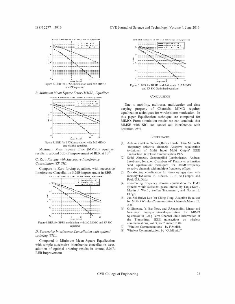
ISSN 2277 – 3916 CVR Journal of Science and Technology, Volume 4, June 2013
CVR College of Engineering 23
Figure 3. BER for BPSK modulation with 2x2 MIMO
and ZF equalizer
B. Minimum Mean Square Error (MMSE) Equalizer
Figure 4. BER for BPSK modulation with 2x2 MIMO
and MMSE equalizer
Minimum Mean Square Error (MMSE) equalizer
results in around 3dB of improvement of BER at 10-3
C. Zero Forcing with Successive Interference
Cancellation (ZF-SIC)
Compare to Zero forcing equalizer, with successive
Interference Cancellation 3.2dB improvement in BER.
Figure4. BER for BPSK modulation with 2x2 MIMO and ZF SIC
equalizer
D. Successive Interference Cancellation with optimal
ordering (SIC).
Compared to Minimum Mean Square Equalization
with simple successive interference cancellation case,
addition of optimal ordering results in around 5.0dB
BER improvement
Figure 5. BER for BPSK modulation with 2x2 MIMO
and ZF SIC Optimized equalizer
CONCLUSIONS
Due to mobility, multiuser, multicarrier and time
varying property of Channels, MIMO requires
equalization techniques for wireless communication. In
this paper Equalization technique are compared for
MIMO. From simulation results we can conclude that
MMSE with SIC can cancel out interference with
optimum level.
REFERENCES
[1] Ardavn malekhi- Tehrani,Babak Hasibi, John M. coeffi
‘frequency selective channels Adaptive equalization
techniques of Multi Input Multi Output’ IEEE
Transaction. Wireless Communication 1999.
[2] Sajid Ahmed¤, Sangarapillai Lambotharan, Andreas
Jakobsson, Jonathon Chambers of’ Parameter estimation
‘and equalization techniques for MIMOfrequency
selective channels with multiple frequency offsets.
[3] Zero-forcing equalization for timevaryingsystem with
memory“byCassio B. Ribeiro, L. R. de Campos, and
Paulo S.R.Diniz.
[4] zero-forcing frequency domain equalization for DMT
systems within sufficient guard interval by Tanja Karp ,
Martin J. Wolf , Steffen Trautmann , and Norbert J.
Fliege.
[5] Jun Shi Huiyu Luo Yu-Ching Tong, Adaptive Equalizer
for MIMO WirelessCommunication Channels March 12,
2003.
[6] O. Simeone, Y. Bar-Ness, and U.Spagnolini, Linear and
Nonlinear Preequalization/Equalization for MIMO
SystemsWith Long-Term Channel State Information at
the Transmitter, IEEE transactions on wireless
communications, vol. 3, no. 2, march 2004.
[7] ‘Wireless Communications’ by F.Molish
[8] Wireless Communication, by “GoldSmith”

ISSN 2277 – 3916 CVR Journal of Science and Technology, Volume 4, June 2013
24 CVR College of Engineering
A Continuous-Time ADC and Digital Signal
Processing System for Smart Dust and Wireless
Sensor ApplicationsB. Janardhana Rao
1 and O.Venkata Krishna
2
1 CVR College of Engineering/ECE, Hyderabad, India
Email: [email protected] 2 CVR College of Engineering/EIE, Hyderabad, India
Email: [email protected]
Abstract— In this paper an event-driven (ED) digital signal
processing system (DSP), Analog-to-digital converter(ADC)
and Digital-to-analog converter(DAC) operating in
continuous-time (CT) with smart dust as the target
application is presented. The benefits of the CT system
compared to its conventional counterpart are lower in-band
quantization noise and no requirement of a clock generator
and anti-aliasing filter, which makes it suitable for
processing burst-type data signals.
A clock less EDADC system based on a CT delta
modulation (DM) technique is used. The ADC output is
digital data, continuous in time, known as “data token”. The
ADC used an un buffered, area efficient, segmented resistor
string (R-string) feedback DAC. This DAC in component
reduction with prior art shown nearly 87.5% reduction of
resistors and switches in the DAC and the D flip-flops in the
bidirectional shift registers for an 8-bit ADC, utilizing the
proposed segmented DAC architecture. The obtained Signal
to noise distortion ratio (SNDR) for the 8-bit ADC system is
55.73 dB, with the band of interest as 220 kHz and Effective
number of bits(ENOB) of more than 9 bits.
Index Terms: smart dust, continuous-time (CT), Delta
modulation, Analog-to-digital converter (ADC), Digital-to –
analog converter (DAC).
I. INTRODUCTION
The target of this paper is to study and design a
mixed-signal processing system consisting of an Analog-
to-Digital Converter (ADC), Digital Signal Processor
(DSP) and Digital-to-Analog Converter (DAC), for the
smart dust application, in a top-down, test-driven design
methodology. The complete system has to be operated in
a CT mode without any sampling. The focus is to achieve
low power consumption and area, without sacrificing the
overall system performance.
There has been a new phenomenon emerging out in
recent past called “smart dust” also known as “motes” or
“wireless sensor networks” or “swarming”. Smart dust is
a tiny (size and density of a sand particle), ultra-low-
power electronic sensory autonomous device packed with
various sensors, intelligence and even wireless
communication capability. A typical scenario could be
smart dust motes deployed in large numbers to form an
ad-hoc network, called as swarm, detects environment
variables such as light, temperature, pressure, vibration,
magnetic flux density or chemical levels. This network,
formed by few tens or even millions of motes, can
communicate with neighboring motes and pass on the
data collected from one mote to another in a systematic
way, which can be collected and processed further [1].
Smart dust can derive the energy necessary for its
functioning either from batteries or from the environment
itself, or from both. The power consumption of the smart
dust decreases with the shrinkage in the size of the mote.
It has to be in the order of few microwatts. This imposes
a stringent constraint on the design, and has to be
addressed by following various low power design
techniques.
Figure 1. Block diagram of a typical smart dust mote.
Figure.1 shows the block level details of a single
autonomous smart dust supply regulator, control, high-
speed sensor interface, low-speed sensor interface, DSP
and radio transceiver section. Energy harvester generates
energy from the environment such as solar radiation,
wind or even vibration. The generated energy is stored
for future usage, using an energy storage element. The
available energy is supplied efficiently, in the form of
fixed voltages and currents, to the various circuits of the
system with the help of the supply regulator. The control

ISSN 2277 – 3916 CVR Journal of Science and Technology, Volume 4, June 2013
CVR College of Engineering 25
circuitry is responsible for the various control
mechanisms involved in a mote, which decides the
operation of the mote. The sensors collect the
environmental variations of interest and convert them to
an equivalent electrical signal, analog in nature. The
sensory interfaces are required to perform initial signal
conditioning and analog to digital conversion of the
sensed data. The data is processed digitally using a DSP.
DSPs can essentially perform various kinds of operations
on the digital signals, such as filtering, domain
transformations, compression, encryption, etc. The
processed data is reconstructed back to analog equivalent
necessary for transmission, using a DAC (not shown in
figure). The transceiver section up-converts the baseband
signal to Radio Frequency (RF) signals and transmits
them. It also receives the RF signals and down-converts
them to the baseband signal. This paper targets the design
of the low speed sensor interface and the DSP, as
highlighted in figure 1.
The specifications of the CTDSP system, that is
finally going to be deployed in the smart dust motes are
shown in table 1. The major constraint imposed on the
system is that all the blocks in the design should be
clockless. Further, the system should be implemented in
90 nm advanced Complementary Metal Oxide
Semiconductor (CMOS) process. The specifications of
the ADC, DAC and the transversal direct-form Finite-
Impulse-Response (FIR) Low Pass Filter (LPF) is as
shown in table 1.
TABLE 1.
SPECIFICATIONS OF THE CT-DSP SYSTEM FOR SMART DUST.
A. Continuous time processing
A new emerging field of digital signal processing in
CT has been presented by Prof. Yannis Tsividis of
Columbia University [2, 3]. It is opposed to the
conventional sampled systems where the processing is
carried out in discrete time. This CTDSP system
processes the data sensed by the analog Interface block
of the sensor module and produce the output to the RF
front-end. As the input data is of burst nature, occurring
occasionally, it is highly desirable that the CTDSP system
remains idle most of the time and operates only when
there is a significant data to process. This is achieved by
using level crossing technique, where the ADC operates
only if there is a significant variation observed in the
input signal. It doesn’t produce a sample if there is a long
silence or no data available to process.
A conventional DSP system operates with a global
reference or clock signal. The input signal, x(t), is
sampled-and-quantized at the rising or falling edge of the
clock signal for an edge triggered system. The quantized
signal is encoded digitally and processed by the
subsequent DSP section and the reconstruction of the
digital signal to the analog equivalent by the output
DAC.. The overall system is completely synchronized
with respect to the global clock. The drawbacks of the
conventional DSP systems are, A sampled system
requires clock generator, which has a large fan-out, since
it has to drive gates of many transistors. Hence, making it
costly to implement, both in terms of the area and power
consumption, the sampling frequency is decided based on
the highest frequency component of the input signal. It is
therefore necessary to implement a band-limiting filter
known as an anti-aliasing filter, to avoid aliasing, whose
implementation might also be a costly affair, the
sampling results in the aliasing of higher frequency terms
to the band of interest, even if the Nyquist theorem is
followed and the deviation from the precise sample
timing instances due to the clock jitter and the clock skew
can cripple down the system performance to undesired
levels, if not designed properly.
The signal to be processed by the smart dust module
is of burst nature, which occurs occasionally. The clocked
systems, although equipped with many advantages, are
not an ideal choice for processing the burst-like signals.
The drawbacks listed for the clocked system are more
dominating compared to the advantages for the smart
dust application. Hence in this paper the event-driven CT
digital signal processing systems are discussed, which
operates on the principle of level-crossing and are very
suitable for burst-type data processing.
II. CONTINUOUS-TIME OR EVENT-DRIVEN DSP SYSTEMS
The CT or event-driven Digital Signal Processor
(DSP) systems, as the name suggests, operates in
continuous time mode [2,6]. The input signal, x(t), is
processed by the CTDSP system to produce output, y(t).
There is no clock involved anywhere in the system. A
CT system can also be divided into three basic sub-
systems: the CTADC, CTDSP and CTDAC. As pointed
out above, there is no global clock involved anywhere in
CTDSP system. Hence, all the three blocks operates in a
CT mode and are represented with a prefix CT [5]. Figure
2 shows the block diagram of the CTDSP system with the
three sub-systems. CTADC is the first block in the
CTDSP system which quantizes and digitizes the input
signal, x(t), to a CT output, bi(t). Unlike conventional
system, the input signal is not sampled before
quantization. The CT data is then processed by the
Item Parameter Value
ADC Resolution 8 bits
Maximum input signal
frequency
20 KHz
LPF Sampling frequency 44 KHZ
Passband edge frequency 5.2 KHZ
Stopband edge frequency 10KHz
Pass band ripple 1 dB
Stopband attenuation 50dB
DAC Resolution 8
Generic Supply voltage 1 V
Technology 90nm

ISSN 2277 – 3916 CVR Journal of Science and Technology, Volume 4, June 2013
26 CVR College of Engineering
CTDSP sub-system to produce digital data, dj(t), which is
reconstructed to analog signal, y(t), by the CTDAC block.
Note that the time domain is represented in “t” as it is
always continuous in nature.
Figure 2. CTDSP system with the basic building blocks CTADC-
CTDSP-CTDAC.
The CTDSP system adopts non-uniform sampling
approach, where samples are generated only when the
event crosses predefined quantization reference level. The
operation of the CTDSP system can be classified as
quantization by the CTADC block and the processing of
the digital (continuous) data by the CTDSP subsystem.
A. CTDSP quantization technique: A level-crossing
approach.
A conventional DSP system adopts uniform
quantization technique, where samples are taken and
processed at every clock cycle. The maximum frequency
of the input signal dictates the minimum possible clock
frequency of sample generation. However, it turns out
that, for signals with burst-like nature and long period of
silence, exhaustive sampling is not required as done in
conventional systems. The samples generated either
contains no information or repetitive information.
Further, additional dynamic power is required for the
processing of these samples by the DSP section. A
different class of the quantization technique, called a
level-crossing sampling scheme, suggested by Sayiner et
al., and further explained by Tsividis in [2, 3, 5]. It is a
non-uniform sampling approach, where the samples are
generated only when the event crosses the predefined
quantization reference level. Since the quantization is
based on the event and is continuous in time, it is called
as an EDCT quantization [3].
The quantization steps can be uniform or non-
uniform and can be customized further based on the
application. To understand the CT quantization
technique, let’s consider figure.3. As shown, the input
signal, x(t), when crosses the predefined quantization
reference level, get quantized to signal, xq(t), and
produces samples (ti, x(ti)). This is a non-uniform
sampling operation, where the signals with faster slope
generates samples more frequently (“faster”) compared to
signals with lesser slopes. Hence, signal-dependent
sampling is achieved simply by utilizing the built-in
feature of the quantizer. With this approach, the signal
with less variation produces lesser number of samples to
be processed by the subsequent DSP section; hence
resulting in a signal dependant power consumption. This
is a clear advantage of the CT systems, making it very
suitable for processing burst type signals.
The continuous-time digital output, bi(t), of the
CTADC block is processed by the CTDSP sub-system.
Since the ADC output is digital in nature, the advantages
of the digital signal processing can be utilized in the CT
system as well. The design approach for the CTDSP
system is described in [6]. Based on the transfer function,
a conventional DSP system can be realized using
multipliers, adders and delay taps as basic building
blocks. A digital signal processor operating in the CT
mode can be mapped from the discrete counterpart by
replacing these blocks by the one operating in the CT
domain. For Example, asynchronous multipliers and
adders, which operates without clock, can be used in the
CT system. One method of implementing the delay taps
is by using chain of inverters. A better approach is
presented in [9,10], where collection of delay cells
connected in series are used to delay and hold the data.
Handshaking is used between delay cells to ensure proper
data transmission. The usage of these delay blocks are
experimentally confirmed in [4, 11]. The CTDSP sub-
system produces output, dj(t), as shown in figure 2, which
is reconstructed back to the analog equivalent, y(t), by the
CTDAC module. The CTDAC can be realized using
architectures and circuit implementation techniques as
mentioned in section V for the clocked counterpart. The
only difference is that the DAC should operate without
clock.
Figure 3. Level-crossing quantization technique in CTDSP system
III. EVENT-DRIVEN ADC
The first module in the ED DSP system is the
CTADC or the ED ADC. It converts the analog input
signal, x(t), provided by the Analog Interface (AI) to CT
digital binary output signal, bi(t). A block diagram of the
AI and the CTADC is shown in figure 4. The AI section

ISSN 2277 – 3916 CVR Journal of Science and Technology, Volume 4, June 2013
CVR College of Engineering 27
consists of a sensor network and an analog filter. The
sensor network detects the variation in the input signal
(temperature, pressure, humidity , etc. based on the
application) and converts it to the electrical signal. The
analog filter limits the frequency of the input signal to the
operating range of the ADC.
Figure 4. Block diagram of AI and CTADC.
The AI is designed based on the overall specification
defined for the smart dust module, for e.g., the sensor
interface is selected based on the application and the
cutoff frequency of the analog filter is selected based on
the frequency of operation of the system. As illustrated in
figure 4, the AI provides a CT signal, x(t), to the CTADC
block. The CTADC consists of a CT quantizer and an
encoder, which digitize the signal to, bi(t). The digital
output, bi(t), is continuous in time and can be represented
in many ways depending on the deployed ADC
architecture [3].
A .Level-crossing sampling for the CTADC
The CTADC adopts a level-crossing sampling
technique. In this section a detailed description of the
level-crossing quantization technique is presented.
Figure. shows the quantization procedure in the CTADC.
When the input signal, x(t), crosses a quantization
reference level, it gets quantized to the nearest
quantization level based on the direction of the input
signal. The quantized signal, xq(t), as shown in figure 5,
is continuous in time and the samples are represented as
(ti, x(ti)), where ti−1 and ti represent the time instances of
the sample generation, respectively. The quantized signal,
xq(t), can be digitized in many ways [3], like the CT
binary bits in a flash ADC or by using data token
consisting of change and direction (increment/decrement)
as in DM [15]. The former approach is illustrated in
figure.5, where b0, b1 and b2 are the CT binary signals.
The level-crossing sampling is a non-uniform sampling
operation, where the faster signals with higher slopes
generate samples more frequently (“faster”) compared to
signals with lower slopes. Hence, a signal-dependent
sampling is achieved
Figure 5. Level-crossing quantization in the CTADC with 3-bit CT
digital output representation; b0, b1 and b2.
simply by utilizing the built-in feature of the quantizer. It
means, that an input signal with lower variation generates
lower number of samples to be processed by the
subsequent DSP section, hence achieving lower dynamic
power dissipation.
The frequency spectrum of an 8-bit CT quantizer as
well as the sampled quantizer are shown in figure 6 and
figure.7, respectively. The CT quantized signal spectrum
has only the signal and its harmonic components.
Whereas, the output spectra of the conventional sampled
quantizer contains not only the signal and its harmonics,
but also other undesirable tones, which are spread across
the entire spectrum, and are not harmonically related to
the signal frequency. This is an artifact due to aliasing of
the higher frequency harmonic distortion components
into the lower frequency band of interest and can be
attributed to the sampling of the CT quantized output,
which is just same as the conventional technique of
quantization after sampling. Hence the difference
between figure.6 and figure.7 is the noise floor added in
the latter case due to aliasing, which is an inherent feature
of sampling.
Figure 6: Frequency spectrum of an 8-bit CT quantizer with input
amplitude A = xmax.
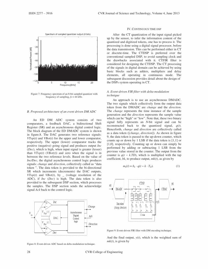
ISSN 2277 – 3916 CVR Journal of Science and Technology, Volume 4, June 2013
28 CVR College of Engineering
Figure 7: Frequency spectrum of an 8-bit sampled quantizer with
frequency of sampling, fs = 44 kHz.
B. Proposed architecture of an event driven DM ADC
An ED DM ADC system consists of two
comparators, a feedback DAC, a bidirectional Shift
Register (SR) and an asynchronous digital control logic.
The block diagram of the ED DMADC system is shown
in figure.8. The DAC generates two reference signals:
VTop(t) and VBot(t) for the upper and lower comparator,
respectively. The upper (lower) comparator tracks the
positive (negative) going signal and produces output Inc
(Dec), which is high, when input signal is greater (lesser)
than VTop(t) (VBot(t)) and zero when the signal is in
between the two reference levels. Based on the value of
Inc/Dec, the digital asynchronous control logic produces
signals: change and direction, collectively called as “data
token ”. The data token is provided to the bi-directional
SR which increments (decrements) the DAC outputs,
VTop(t) and VBot(t), by _ (voltage resolution of the
ADC), if Inc (Dec) is high. The data token is also
provided to the subsequent DSP section, which processes
the samples. The DSP section sends the acknowledge
signal Ack back to the control logic.
Figure 8: Event-driven ADC based on delta modulation technique.
IV. CONTINUOUS TIME DSP
After the CT quantization of the input signal picked
up by the sensor, to infer the information content of the
quantized and digitized tokens, one has to process it. The
processing is done using a digital signal processor, before
the data transmission. This can be performed either in CT
or discrete-time. The CTDSP is preferred over the
conventional sampled DSP, to avoid sampling clock and
the drawbacks associated with it. CTFIR filter is
considered for designing the CTDSP. The CT processing
of the signals in digital domain can be achieved by using
basic blocks such as adders, multipliers and delay
elements, all operating in continuous mode. The
subsequent discussion provides detail about the design of
the DSPs system operating in CT.
A. Event-driven FIR filter with delta-modulation
technique
An approach is to use an asynchronous DMADC.
The two signals which collectively form the output data
token from the DMADC are change and the direction.
The change represents the time instance of the sample
generation and the direction represents the sample value
which can be “high” or “low”. Note that, these two binary
signal fully represents an N-bit signal and can be
reconstructed back to the quantized signal, q(t).
Henceforth, change and direction are collectively called
as a data token ([change, direction]). As shown in figure
9, the data token is passed to the up-down counter, which
counts up or down by 1 LSB if the data token is [1,1] or
[1,0], respectively. Counting up or down can simply be
performed by adding or subtracting 1 LSB from the
previous value stored in the counter. The output from the
counter is q(t − k.TD), which is multiplied with the tap
coefficient, bk, to produce output, mk(t), as given by
mk(t) = bk · q(t − k · TD). (1)
Figure 9: Event-driven FIR filter with DM encoding technique.
And the final output, y(t), which is the weighted sum of
mk(t), is given by

ISSN 2277 – 3916 CVR Journal of Science and Technology, Volume 4, June 2013
CVR College of Engineering 29
(2)
B. Design consideration of CTDSP system
In this section a few basic design parameters are
discussed that are required for designing the CTDSP
system. A transfer function of the CTDSP system is the
filter transfer function, B(s), can be determined by taking
the Laplace transform of output, y(t), as given by
equation (2), where y(t) is represented as the linear
combination of the quantized input signal, q(t). The
output Y (s) of a system with frequency response, B(s),
and a quantized input signal Q(s) is given by
Y (s) = Q(s) · B(s). (3)
The expression for Y (s) can be written as
(4)
The data token generated by the CTADC depends on
the slope of the input signal. The total number of data
tokens generated and the minimum possible distance
between the two tokens are of primary importance, as it
defines the functional requirement on the DSP section.
Both, the number and the distance between the two data
tokens has to be preserved, to achieve the correct filtering
operation by the DSP block. Any missing data token or
deviation in the distance between the two tokens, may
result in undesirable variation in the frequency response
of the filter.
The CTADC should be able to operate at the rate of
1/Tmin, which for the above case of fb= 20 kHz is
approximately equal to 16 MHz. This is equivalent to
oversampling the ADC by a rate of 400. Hence, this
system is suitable only for low frequency operation,
because, for the high input frequency and considering the
same oversampling ratio, the data token rate goes
drastically high, which can be impractical for
implementation with the mainstream CMOS process.
Based on the above discussion and design parameters, fb
and N of the ADC, it is possible to roughly define the
power consumption of the CTDSP system.
V. CONTINUOUS TIME DAC
The CTDAC is the final block of the CTDSP system.
It converts the digitally processed CTDSP sub-system
output to an analog equivalent. In the previous sections, it
is concluded that the DM-based ADC and DSP are
preferred architectures for the smart dust application.
Hence, the DAC architecture selection is based on the
assumption that it is capable of accepting the 8-bit output
word from the DM operated DSP sub-system. Also, as
shown in figure 8, one feedback DAC is required inside
the CTADC block. Hence, there are two DACs in the
complete system. Target of the design is to reuse the
same architecture in both the places. Any DAC which
work asynchronously can be used for this purpose.
Few important points to take care, while selecting the
DAC architecture, which is suitable for the feedback as
well as the output DAC, are: The CTDAC shall generate
two reference levels VTop(t) and VBot(t) required as a
reference for the top and bottom comparators shown in
figure 8. The two reference levels are separated by LSB
given by equation (2)
VTop(t) − VBot(t) = LSB. (2)
Note that this constraint is not applicable for the
output DAC, where only one output is required. The
output shall increment or decrement by only one bit at a
time to track the input signal continuously in the
DMADC. It shall operate in an asynchronous mode
without any clock, as no clock is used in the other sub-
modules. It shall occupy very less area and it shall
consume as less power as possible.
There are many possible architectures which can be
used for realizing the required DAC structure with the
constraints given above, e.g., resistor-string (R-string),
current steering DAC, charge accumulation DAC and
segmented DAC [7]. It has been shown in [11], that a
resistor-string DAC architecture occupies lesser area,
consumes less power, simple in design and can generate
the two reference levels as described above. Due to these
advantages a resistor-string DAC architecture is selected
in this design.
A. Segmented resistor-string DAC
It is described that the resistor-string DAC
architecture is preferred over the other DAC
architectures. However, the simple resistor-string DAC
may not be a cost effective solution for higher ADC is to
use segmented resistor-string architecture, which
produces same resolution as resistor-string architecture,
with less hardware. Various possible segmented DAC
architectures are available with the advantages and
drawbacks. A final DAC architecture is presented, which
is used in the design and block diagram is shown in
figure 10.
The segmented m × n resistor-string DAC consists of
two segments, where the first string with m resistors,
resolves the Most Significant Bits (MSBs) and the second
substring with n resistors, resolves the Least Significant
Bits (LSBs) [7].
As shown in figure.10, two bi-directional SRs are
required in this architecture, which based on the data
token, produces m and n bit control signals for the MSB
and LSB string, respectively. One possible selection of m
and n is given by

ISSN 2277 – 3916 CVR Journal of Science and Technology, Volume 4, June 2013
30 CVR College of Engineering
Figure 10: Block diagram of the m × n segmented resistor-string DAC
with the m × n segmented bi-directional Shift registers.
(5)
Figure.11 presents the segmented resistor-string DAC
architecture with the MSB and LSB strings. Vref,high and
Vref,low are the highest and lowest output reference
voltages, respectively, from the DAC and are applied
across the MSB string. The control signals, m and n from
the bi-directional SR, are applied to the switches used to
tap the output of the MSB and LSB string, respectively.
Only one output is high at a time for each m and n bits.
The total number of resistors in the segmented DAC and
the total number of flip-flops in the bi-directional SR are
now given by (m+n) and the total switches in the DAC
are given by (2) · (m+n). The voltage step, MSB, resolved
by each resistor in the MSB string is given by
(6)
which is further resolved by the LSB string to voltage
step, , given by
(7)
where m·n = 2N. Hence, the segmented architecture
produces the same resolution as obtained by an N-bit
resistor-string DAC, with reduced hardware count.
This architecture, however, suffers from the loading
effect of the LSB string to the tapped MSB resistor as
explained next. Let RMSB and RLSB be the respective
resistances of each resistor in the MSB and the LSB
string. The total series resistance of LSB string, RLSB,T otal,
is given by
RLSB,T otal = n.RLSB. (8)
The equivalent resistance, RMSB,Equivalent, of the tapped
MSB resistor in parallel to RLSB,T otal is given by
RMSB,Equivalent = RMSB || (n.RLSB), (9)
which is different from RMSB. Hence, the voltage drop
across the tapped MSB resistor is not exactly equal to
MSB, as given by equation (6). It results in the generation
of incorrect reference voltages at the output of the DAC.
The loading effect of the LSB string to the MSB string
can be avoided simply by adding buffers between the
MSB and the LSB string then
RMSB,Equivalent = RMSB. (10)
It means, that effectively there are m resistors in
series in the MSB string, with each resistor generating
MSB as given by equation (6), which is exactly the same
as required. Hence, with the proper choice of LSB string
resistors, the loading effect can be avoided.
VI. SIMULATION RESULTS
Systematic top-down test-driven methodology is
employed throughout the project. Initially, MATLAB
models are used to compare the CT systems with the
sampled systems. The complete CTDSP system is
implemented in Cadence design environment. The
architecture of the DM ADC system ,as shown in Fig.8. is
used to realize a high level working model of an 8- bit
ADC system employing the proposed segmented DAC
architecture.
Figure 11: Resistor-string segmented DAC architecture.
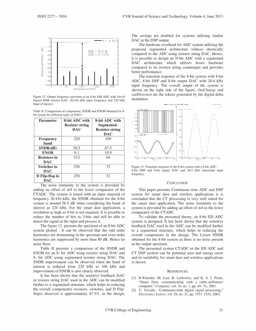
ISSN 2277 – 3916 CVR Journal of Science and Technology, Volume 4, June 2013
CVR College of Engineering 31
Figure 12. Output frequency spectrum of an 8-bit DM ADC with 16×16
shared MSB resistor DAC, 20.416 kHz input frequency and 220 kHz
band of interest.
Table II. Comparision of components, SNDR and ENOB obtained for 8-
bit system for different types of DACs.
Parameter 8-bit ADC with
Resister string
DAC
8-bit ADC with
Segmented-
Resister-string
DAC
Frequency
band
220 100
SNDR(dB) 56.5 67.5
ENOB 9.1 10.9
Resisters in
DAC
512 64
Switches in
DAC
256 33
D Flip-flop in
DAC
256 32
The noise immunity to the system is provided by
adding an offset of /4 to the lower comparator of the
CTADC. The system is tested with an input sinusoid of
frequency 20.416 kHz, the SNDR obtained for the 8-bit
system is around 56.5 dB when considering the band of
interest as 220 kHz. For the smart dust application, a
resolution as high as 8-bit is not required. It is possible to
reduce the number of bits to 3-bits and still be able to
detect the signal at the input and process it.
The figure 12. presents the spectrum of an 8-bit ADC
system plotted . It can be observed that the odd order
harmonics are dominating in the spectrum and even order
harmonics are suppressed by more than 80 dB. Hence no
noise floor.
Table II presents a comparison of the SNDR and
ENOB for an 8- bit ADC using resister string DAC and
8- bit ADC using segmented resister string DAC. The
SNDR improvement can be observed when the band of
interest is reduced from 220 kHz to 100 kHz and
improvement of ENOB is also clearly observed.
It has been shown that the sensitive feedback DAC
or resistor string DAC used in the ADC can be modified
further to a segmented structure, which helps in reducing
the overall components( resistors, switches, and D Flip-
flops) observed is approximately 87.5%. in the design.
The savings are doubled for systems utilizing similar
DAC at the DSP output.
The hardware overhead for ADC system utilizing the
proposed segmented architecture reduces drastically
compared to the ADC using resistor string DAC. Hence,
it is possible to design an N-bit ADC with a segmented
DAC architecture which utilizes lesser hardware
compared to its resistor string counterpart and provides
better performance.
The transient response of the 8-bit system with 8-bit
ADC, 8-bit DSP and 8-bit output DAC with 20.4 kHz
input frequency. The overall output of the system is
shown on the right side of the figure, OutChange and
outDirection are the tokens generated by the digital delta
modulator.
Figure 13. Transient response of the 8-bit system with a 8-bit ADC,
8-bit DSP and 8-bit output DAC and 20.4 kHz sinusoidal input
frequency.
CONCLUSION
This paper presents Continuous time ADC and DSP
system for smart dust and wireless applications it is
concluded that the CT processing is very well suited for
the smart dust application. The noise immunity to the
system is provided by adding an offset of /4 to the lower
comparator of the CTADC.
To validate the presented theory, an 8-bit ED ADC
system is designed. It has been shown that the sensitive
feedback DAC used in the ADC can be modified further
to a segmented structure, which helps in reducing the
overall components in the design. The Lower SNDR
obtained for the 8-bit system as there is no noise present
in the output spectrum.
The presented system CTADC or the ED ADC and
CT DSP section can be potential area and energy saver
and its suitability for smart dust and wireless applications
is shown.
REFERENCES
[1] B.Warneke, M. Last, B. Liebowitz, and K. S. J. Pister,
“Smart Dust: communicating with a cubic-millimeter
computer,” Computer, vol. 34, no. 1, pp. 44– 51, 2001.
[2] Y. Tsividis, “Continuous-time digital signal processing,”
Electronics Letters, vol. 39, no. 21, pp. 1551–1552, 2003.

ISSN 2277 – 3916 CVR Journal of Science and Technology, Volume 4, June 2013
32 CVR College of Engineering
[3] Y. Tsividis, “Event-Driven Data Acquisition and Digital
Signal Processing_A Tutorial,” Circuits and Systems II:
Express Briefs, IEEE Transactions on, vol. 57, no. 8, pp.
577–581, 2010.
[4] B. Schell and Y. Tsividis, “A Continuous-Time
ADC/DSP/DAC System With No Clock and With
Activity-Dependent Power Dissipation,” Solid-State
Circuits, IEEE Journal of, vol. 43, no. 11, pp. 2472–2481,
2008.
[5] Y. Tsividis, “Digital signal processing in continuous time:
a possibility for avoiding aliasing and reducing
quantization error,” in Acoustics, Speech, and Signal
Processing, 2004. Proceedings. (ICASSP ’04). IEEE
International Conference on, vol. 2, pp. ii–589–92 vol.2,
2004.
[6] Y. Tsividis, “Event-driven data acquisition and continuous-
time digital signal processing,” in Custom Integrated
Circuits Conference (CICC), 2010 IEEE, pp. 1–8, 2010.
[7] D. Johns and K. W. Martin, Analog integrated circuit
design. New York: Wiley, 1997.
[8] B. Schell and Y. Tsividis, “Analysis and simulation of
continuous-time digital signal processors,” Signal
Processing, vol. 89, pp. 2013–2026, 10 2009.
[9] B. Schell and Y. Tsividis, “A Low Power Tunable
Delay Element Suitable for Asynchronous Delays of
Burst Information,” Solid-State Circuits, IEEE
Journal of, vol. 43, no. 5, pp. 1227–1234, 2008.
[10] M. Kurchuk and Y. Tsividis, “Energy-efficient
asynchronous delay element with wide
controllability,” in Circuits and Systems (ISCAS),
Proceedings of 2010 IEEE International Symposium
on, pp. 3837–3840, 2010.
[11] B. Schell, Continuous-time digital signal processors :
analysis and implementation. PhD thesis, Columbia
University, 2008.

ISSN 2277 – 3916 CVR Journal of Science and Technology, Volume 4, June 2013
CVR College of Engineering 33
FPGA Implementation of OFDM Transceiver R. Ganesh
1 and S. Sengupta
2
1CVR College of Engineering/ECE Department, Hyderabad, India
Email: [email protected] 2 CVR College of Engineering/ECE Department, Hyderabad, India
Email: [email protected]
Abstract—The OFDM is a multi-carrier modulation scheme
in which the available carrier bandwidth can be divided into
N number of orthogonal carrier frequencies and the data
can be shared by these multiple carriers. This paper
describes the design and implementation of OFDM
transceiver using single FPGA board. The design
methodology used is the 8-point IFFT/FFT with radix-2
with QPSK modulation scheme. The design unit consists of
a back to back connected OFDM transmitter and receiver
with QPSK framer, IFFT, PISO, SIPO, FFT and QPSK de
framer etc. All these blocks are designed and simulated
using Xilinx ISE 12.4 design suite. Finally the transceiver is
implemented on Xilinx Virtex 5 LX110T FPGA with a data
rate of 8, 16, 32 Mbit.
Index Terms— OFDM, FFT, IFFT, FPGA, QPSK
I. INTRODUCTION
The growth of the wireless communication has
produced a strong demand for advance wireless
communication. Orthogonal Frequency Division
Multiplexing (OFDM) is a state of the art modulation
technique for high speed wireless communication with
resistant to fading. The OFDM is a special form of Multi
carrier Modulation which was originally used in high
frequency radio. An efficient way to implement OFDM
by means of Discrete Fourier Transform (DFT).The
computational complexity would be reduced by a Fast
Fourier Transform (FFT).Recent advances in VLSI
Technology have enabled cheap and fast implementation
of FFT’s and IFFT’s.
The data transmission over a wireless communication
channel can be done by using a carrier signal with the
help of modulation. The transmission can be done by
using either a single carrier modulation or multi carrier
modulation. In a single carrier modulation scheme each
data symbol is transmitted sequentially on a single carrier i.e. signaling interval equal to data symbol duration [4].
The problem with single carrier modulation is the
modulated carrier is occupies the entire available
bandwidth. This problem can be solved by using multi
carrier modulation. In a multi carrier modulation scheme
N sequential data symbols are transmitted simultaneously
on N multiple carriers i.e. signaling interval equal to N
time’s data symbol duration [4]. Here the available band
width is divided into N number of sub carriers; hence it is
bandwidth efficient compared to single carrier
modulation.
The Orthogonal Frequency Division Multiplexing
(OFDM) is one of the multi carrier modulation
techniques for data transmission. In OFDM all the sub
carriers are orthogonal to each other. The concept of
conventional multi carrier and orthogonal multi carrier
techniques are shown in Fig.1 (a) and Fig.1 (b) [5].
Figure. 1(a) Conventional Multi carrier technique
Figure. 1(b) Orthogonal Multi carrier technique
The Fig.2 shows block diagram of OFDM transmission
system. The design consists of OFDM transmitter and
receiver with different sub blocks. The OFDM transmitter
accepts the serial data and this data is grouped in to n-bits
and applied to IFFT through a bulk modulator like QPSK.
The IFFT converts frequency domain signals into time
domain signals and these signals are transmitted to
receiver through parallel in serial out shift register with I
(real) and Q (imaginary) channel data. At the receiver the
received time domain data symbols are grouped with
serial in parallel out and converted into frequency domain
by using FFT with QPSK demodulation. The parallel
frequency domain data is recovered in serial order using
parallel in serial out shifter.
Figure.2 Block diagram of OFDM transmission system.
The objective of this paper is to develop the single
FPGA based OFDM transceiver using bulk modulator
and demodulator for high speed data transmission on

ISSN 2277 – 3916 CVR Journal of Science and Technology, Volume 4, June 2013
34 CVR College of Engineering
wireless media. The modulation is with QPSK and 8 sub
carriers are used.
The 8-point IFFT/FFT is designed by using the fast
implementation of IDFT/DFT equations using butterfly
diagrams. The equation for DFT is given by [3].
Where X(k) indicates the DFT of x(n) sequence and
WN nk
is the twiddle factor of the transform. The equation
for IDFT is given by [3].
Where the x(n) is the inverse DFT of X(k), here n=8
and k=8.
The FPGA implementation of OFDM test set up with
synthesis is explained in section II and Simulation results
of each block is explained in section III. The FPGA
implementation results are explained in section IV then
conclusion in section V and references.
II. THE FPGA IMPLEMENTATION OF OFDM TEST SETUP
The FPGA implementation of OFDM needs a test
setup. To provide the test set up the Fig.1 can be modified
by removing two radios channels and directly connect the
I/Q output values of transmitter to 1/Q input values of
receiver. This setup will provide a back to back
connected OFDM transmitter and receiver namely
OFDM transceiver. This OFDM transceiver FPGA
implementation test setup is shown in the Fig.3. The
design is tested for 8, 16, 32 Mbit by using proper
selection of input switches of FPGA.
Figure.3 FPGA Implementation of OFDM transceiver test setup
The FPGA implementation of OFDM transceiver can
be designed by using following blocks.
A. Counter
The serial I/P data to the OFDM transmitter can be
applied by using a 16-bit counter. The 16-bit data is
applied to QPSK framer.
B. QPSK framer
The QPSK framer accepts 16-bit data and converts
every two bits data in to real and imaginary of
constellation mapping as shown in Table 1. This QPSK
framer block produces eight real and eight imaginary data
values. TABLE I
QPSK mapping
Input data Output
00 1+j0
01 0+j1
10 -1+j0
11 0+j(-1)
C. IFFT
The eight complex pair outputs of QPSK framer is
connected to the IFFT and the conversion from frequency
domain to time domain can be done by using IEEE 754
floating point arithmetic operations on data and twiddle
factors.
D. PS and SP (Parallel in Serial out and Serial in
Parallel out)
The eight complex pair time domain IFFT output data
(i.e. OFDM frame) is applied to PS and the output is
taken serially and transmitted directly to the receiver first
stage i.e. SP. The SP accepts serial input data from PS
one after another and generates eight complex pair data as
output (i.e. OFDM frame).
E.FFT
The eight complex pair outputs of SP (i.e. OFDM
frame) is connected to the FFT and the conversion from
time domain to frequency domain can be done by using
IEEE 754 floating point arithmetic.
F. De framer
The De framer accepts eight complex pair data values
and converts each pair of data in to two bit digital data
according to de framer logic and produces 16-bit digital
data as the output. This received 16-bit data should be
same as the transmitted input data which is the output of
16- bit counter.
G. Clock Divider
The FPGA implementation of OFDM requires a clock
signal frequency. The OFDM design frequency can be
generated by converting the FPGA on-board clock
frequency (i.e. 33Mhz) into different required frequencies
by using the below formula.
Required frequency=On-board frequency/2n
Where ‘n’ indicates the bit position in counter of
frequency divider. Here the OFDM transceiver is running
with three different frequencies of 0.5 MHz, 1 MHz and

ISSN 2277 – 3916 CVR Journal of Science and Technology, Volume 4, June 2013
CVR College of Engineering 35
2 MHz by using proper selection of input switches
available on FPGA board.
H. Display
The eight Most Significant output bits of the OFDM
transceiver is connected to the eight LED indicators of
Xilinx Virtex-5 LX110T FPGA board.
III. SIMULATION RESULTS
The total OFDM transceiver blocks are designed and
simulated and implemented by using Xilinx ISE 12.4
design suite with the sub tools listed in Table 2.
TABLE 2
List of Tools under Xilinx ISE design suite
Design Action Name of the Tool
Design Entry HDL Editor (Verilog)
Synthesis Xilinx Synthesis Tool(XST)
Simulator ISim Simulator
Implementation FPGA Editor, Plan Ahead
Device Configuration iMPACT
The OFDM transceiver has back to back connected
transmitter and receiver blocks. The QPSK framer, IFFT
and PS blocks forms OFDM transmitter.
The OFDM transceiver is designed by using Verilog
Hardware Description Language. The design is
synthesized for generating the net list from the given
specifications for the target FPGA board. The output of
synthesis i.e. RTL schematic view of OFDM transceiver
is shown in Fig.4.
Figure.4 RTL Schematic of OFDM transceiver
The simulation results of all these blocks are shown in
below figures. The Fig.5 shows the simulation results of
OFDM transceiver data input counter.
The Fig.6 shows the simulation results of QPSK
framer by accepting 16-bit input data from counter. This
block generates eight real and eight imaginary modulated
time domain signals.
The Fig.7 shows the simulation results of IFFT of
QPSK framer output and generates eight real and eight
imaginary frequency domain signals.
The IFFT output is connected to parallel in serial out
shift register of transmitter. Since the design is back to
back connected transceiver the parallel in serial out shift
register output is directly connected to the first stage of
receiver i.e. serial in parallel out shift register.
The SP, FFT and deframer forms OFDM receiver. The
SP output is applied to FFT. The Fig.8 shows the
simulation results of FFT. The FFT block generates eight
real and eight imaginary frequency domain signals.
Figure.5 Counter simulation results
Figure.6 QPSK framer simulation
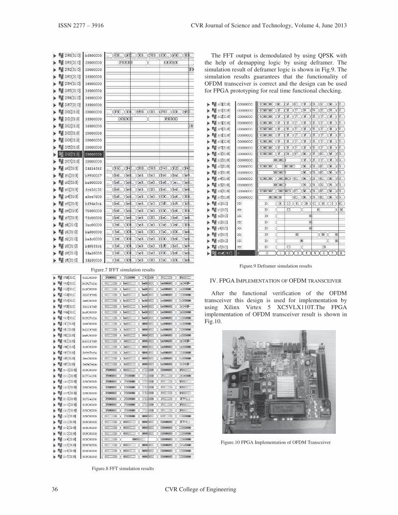
ISSN 2277 – 3916 CVR Journal of Science and Technology, Volume 4, June 2013
36 CVR College of Engineering
Figure.7 IFFT simulation results
Figure.8 FFT simulation results
The FFT output is demodulated by using QPSK with
the help of demapping logic by using deframer. The
simulation result of deframer logic is shown in Fig.9. The
simulation results guarantees that the functionality of
OFDM transceiver is correct and the design can be used
for FPGA prototyping for real time functional checking.
Figure.9 Deframer simulation results
IV. FPGA IMPLEMENTATION OF OFDM TRANSCEIVER
After the functional verification of the OFDM
transceiver this design is used for implementation by
using Xilinx Virtex 5 XC5VLX110T.The FPGA
implementation of OFDM transceiver result is shown in
Fig.10.
Figure.10 FPGA Implementation of OFDM Transceiver

ISSN 2277 – 3916 CVR Journal of Science and Technology, Volume 4, June 2013
CVR College of Engineering 37
CONCLUSIONS
The main focus of this work is to design 8-point
IFFT/FFT based back to back connected OFDM
transceiver using single FPGA. In this work the design,
simulation and implementation of OFDM transceiver
using Xilinx ISE Design suite for Virtex 5 FPGA is
completed. The design functionality is verified for 8, 16,
and 32 Mbit data rates.
The design can be extended by isolating OFDM
transmitter and receiver using two FPGA boards.
REFERENCES
[1] Atul Govindrao Pawar,’’Wireless Communication in Missiles: Challenges’’, Hyderabad, DRDO Science Spectrum, March 2009, pp.230-235.
[2] Hemant Kumar Sharma, Sanjay P. Sood, Balwinder Singh,
”Design of COFDM Transceiver Using VHDL”,
International Journal of Computer Applications (0975 –
8887), Volume 5– No.7, August 2010.
[3] Poonam Agrawal, Vikas Gupta,”Enhanced Core
Processor Blocks of OFDM System”, International Journal
of Electronics Communication and Computer Engineering,
Volume 1, Issue 2, 10/09/2011.
[4] Dr. Miguel Rodrigues,”Orthogonal Frequency Division
Multiplexing: (OFDM A Primer)”, Laboratory for
Communication Engineering, University of Cambridge.
[5] Klaus Witrisal, “Presentation on OFDM Concept and
System-Modeling”, Technical University Graz, Austria,
VL: Mobile Radio Systems, Ch. 5: Wideband Systems,
24-Nov-05.

ISSN 2277 – 3916 CVR Journal of Science and Technology, Volume 4, June 2013
38 CVR College of Engineering
Transmission of Message between PC and ARM9
Board with Digital Signature using Touch Screen R.R. Dhruva
1 and V.V.N.S. Sudha
2
1 CVR College of Engineering, Hyderabad, India.
Email: [email protected] 2 Aurora's Technological and Research Institute, Hyderabad, India.
Email: [email protected]
Abstract—This paper deals with the Transmission of
message between ARM9 board and Personal Computer.
This system can be used as a paperless fax machine. The
main advantage of this paper is to create a paperless office
and to store the fax for future references. Here, a PC is used
as first fax machine and ARM9 board is used as second fax
machine. The message is typed in the System and sent to
ARM9 board. The user can read the message on the touch-
screen and do the digital Signature using Stylus, if required
and send back to the PC. A copy of the message as well as
the Signature is stored in the pen-drive connected to USB of
ARM9 board for future references. The processor used is
S3C2440 and Qtopia is the cross-compiler used. Various
widgets are created in Qtopia using CPP as the
programming language. Firstly, Porting is done in order to
load the Bootloader, Kernel and Root File System. Then
various widgets are created in Qtopia. Ethernet cable is used
to connect the PC and the ARM9 board. Linux Operating
System is used.
Index Terms—ARM9, Qtopia, Porting
I. INTRODUCTION
Samsung S3C2440A is a 16/32-bit RISC
microprocessor. Samsung S3C2440A is designed to
provide hand-held devices and general applications with
low-power, and high-performance micro-controller
solution in small die size. The ARM processor is a
Reduced Instruction Set Computer (RISC). The S3C2440
is a 32 bit microcontroller that internally integrates
ARM920T of the ARM Company [9]. ARM920T
implements 5-stage pipeline architecture and separate
16KB Instruction cache and 16KB Data cache which are
used for faster performance. The S3C2440 have some
integrated on-chip functions such as LCD controller,
RAM controller, 3 paths UART, 4 paths DMA, 4 path
with PWM of Timer, parallel I/O port, 8 channels of 10-
bit ADC, the interface of touch screen, I2C interface, two
USB interface controllers, two channels SPI, the main
frequency of S3C2440 up to 400MHz [4]. The Figure
below shows the MINI2440 on-board peripherals layout.
The Transmission of Message with Digital Signature on
Touch Screen using ARM9 application is implemented in
ARM9 board using QT.
The proposed model consists of S3C2440, PC, Touch
Screen and Ethernet cable. The transmission of data
between S3C2440 and PC is done through this Ethernet
cable.
ARM9 board is considered as one fax machine and PC
as another. The message or fax is sent from PC to board.
The user can do the signature on touch screen of the
board and should click on the save option. A copy of the
message as well as the signature is saved in the pen-drive
for future reference. Single touch panel added to
conventional fax machine-replaces the scanning and
printing units. Touch panel acts as an input device as well
as displaying device, which can detect the location being
touched. Handwriting reconstruction algorithm is used
internally in the board itself to turn a user’s signing act
into a digital signature, close to the original as much as
possible. The document containing the message as well as
the signature is sent back to PC and is seen by typing the
IP address of the board in URL of the web-browser.
Figure 1: Mini2440 Development Board
Qtopia is used to create various components on the
touch screen such as widgets. The operating System used
is Linux and programming is done using CPP.
The procedure for implementing this project is as
follows:
The First step is porting of boot loader , kernel , root
file system into S3C2440 board.
The next step is to develop the application in QT
using CPP.
Then the output can be seen by typing the message
to be transmitted in hyper terminal of personal
computer. Then the message is displayed on the

ISSN 2277 – 3916 CVR Journal of Science and Technology, Volume 4, June 2013
CVR College of Engineering 39
Touch Screen of ARM9 board. Digital Signature is
done using Stylus and a copy of Signature and
message is stored in the pen drive.
The message is again sent back and retrieved on PC
by giving the IP address of board in the URL of
web-browser.
Qtopia is used for set of applications with GUI running
on desktop environment and general application based on
interface. It supports cross compilation for all multiple
boards (open source GUI environment). Qtopia 2.2.0
controls embedded related devices on target board and
compatible with Fedora 9 and ubuntu.
Qt_Embedded is a C++ toolkit for GUI and
application development for embedded devices. It
runs on a variety of processors, usually with
Embedded Linux.
Qt_Embedded based applications write to the Linux
frame buffer directly and includes several tools to
speedup and ease in development in testing and
debugging of applications.
Applications targeted for Embedded Linux can be
developed using standard Qt tools, including Qt
Designer for visual form design, and with tools
specifically tailored to the embedded environment.
II. RESULTS
1) Load the files of bootloader, kernel and file system
into the board by switching the board on, in NOR flash.
2) After loading the above files switch to NAND flash
mode.
3) Restart the board and calibrate the touch screen.
4) Open the port terminal using Debug Port.
5) Open the hyperterminal. Select com1 Port and set
the Baud rate to 115200.
Figure 2: Entering 11,5200 as baud rate
On the Personal Computer we need to enter the
message which has to be transferred to the board.
Figure 3: Entering message on PC
Digital signature is done in the space provided
Figure 4 : Digital Signature done in widget provided
Saving the message as well as the signature by pressing save on
widget in the touch screen.
Figure 5 : Clicking the save option to save a copy of image in the
pen drive
The message as well as the signature is sent back to the
PC. It is observed by typing the IP address of the kit in
the URL of the web-browser.
Figure 6: Retrieval of message as well as digital signature on PC

ISSN 2277 – 3916 CVR Journal of Science and Technology, Volume 4, June 2013
40 CVR College of Engineering
III. CONCLUSION
The model “Transmission of Message with Digital
Signature on Touch Screen using ARM9” has been
successfully designed and tested.
It has been developed by integrating features of all the
hardware components and software used. Presence of
every module has been reasoned out and placed carefully
thus contributing to the best working of the unit.
Secondly, using highly advanced ARM9 board and
with the help of growing technology the project has been
successfully implemented.
IV. FUTURE SCOPE
In the future scope we can go with the usage of touch
screen monitor PC’s where the ARM board can be
directly interfaced to the PC’s. Here in this we are going
to reduce the extra touch screen panel connected to the
ARM board by using touch screen monitors where we
can read the received data and we can do the necessary
modifications require and can send the modified data and
keep the copy of the data inside the memory.
We can also have alert message to your mobiles
whenever a new fax is received and also can have alert
message with voice by using voice play back recorder
circuit like “You received a new FAX ”. In this way we
are reducing the cost and complexity of the circuit. Here
in this concept we are totally eradicating the usage of
paper which reduces the environmental pollution.
REFERENCES
[1] “Linux transplantation based on the processor S3C2440” by
Sun Yanpeng,peng peng,Zhang Yuan, 2009.
[2] Beginning Linux Programming, Third Edition, Neil
Matthew and Richard Stones.
[3] http://www.friendlyarm.net
[4] www.kernel.org
[5] www.linuxjournal.com/magazine
[6] http://www.arm.com/
[7] http://www.w3schools.com/php
[8] http://www.datasheetcatalog.com
[9] ITU-T.37: Procedures for the Transfer of Facsimile Data via
Store-and forward on the Internet, 1998.
[10] ITU-T.38: Procedures for Real-time Group 3 Facsimile
Communication over IP Networks, Amendment 1, 1999.
[11] Handwriting Recognition Group, <hwr.nici.kun.nl>, May,
2008.
[12] ITU-T.4: Standardization of Group 3 facsimile terminals
for document transmission, 1996
[13] ITU-T.30: Procedures for document facsimile transmission
in the general switched telephone network, 1996
[14] http://en.wikibooks.org/wiki/C++_Programming

ISSN 2277 –3916 CVR Journal of Science &Technology, Volume 4, January 2013
CVR College of Engineering 41
A Novel Source Based Min-Max Battery Cost
Routing Protocol for Mobile Ad Hoc Networks Humaira Nishat
1
1 CVR College of Engineering/ECE Department, Hyderabad, India
Email: [email protected]
Abstract—In the existing energy efficient routing protocols
for mobile ad hoc networks such as minimum battery cost
routing (MBCR) and min-max battery cost routing
(MMBCR) the cost functions are calculated in the route
request phase and the decision of selecting a route is taken
by the destination node. It is more cost effective and energy
efficient if the cost functions are calculated in the route
reply phase and the decision of selecting a route for data
transmission is taken by the source node. In this paper I
propose a novel routing algorithm for mobile ad hoc
networks called Source based min-max battery cost routing
(SBMMBCR) protocol wherein the routing decision is taken
by the source node considering the changes in energy levels
during the route reply phase. The performance of the
proposed protocol is compared with the existing MMBCR
protocol based on application oriented metrics such as
throughput, packet delivery ratio, end-to-end delay,
normalized routing load and residual energy. Simulation is
carried out using NS2. From the simulation results it is
observed that the proposed protocol SBMMBCR
outperforms MMBCR by giving more network lifetime as
well as better throughput, packet delivery ration. Average
end-to-end delay is less and the residual energy is also more
for SBMMBCR as compared to MMBCR protocol.
Index Terms—Cost function, Energy level, Routing
protocols, MANETs, Network lifetime, Throughput, Packet
delivery ratio, Delay, Residual energy, Normalized routing
load.
I. INTRODUCTION
Mobile ad hoc networks [MANETS] [10], have
gained significant attention in the past several years due
to the characteristics of being infrastructureless, mobile
and robust. Nodes in MANETS generally rely on
batteries for their operation [4]. Due to the limited
lifetime of these energy sources, battery power [1], [3] is
one of the most important constraints for the operation of
the ad hoc network. Extensive research efforts have been
dedicated to both developing energy efficient protocols
and improving the throughput of a MANET [5], [6], [7].
In this paper I have considered the problem of routing in
an ad hoc network from energy efficiency point of view.
Other quality of service parameters like throughput,
delay, packet delivery ratio, residual energy and routing
overhead are also evaluated and compared with the
existing routing protocol.
The rest of the paper is organized as follows. In section
2 we present the theoretical analysis of existing energy
efficient protocols. The concept of designing the
proposed SBMMBCR protocol is described in section 3.
The simulation scenario is presented in section 4
followed by the simulation results in section 5. Finally,
section 6 concludes the paper.
II. THEORETICAL ANALYSIS OF EXISTING
ENERGY EFFICIENT ROUTING PROTOCOLS
Here I present a brief description of the existing energy
efficient routing protocols-MBCR and MMBCR [2]. In
minimum battery cost routing (MBCR), individual
battery costs are taken into consideration while selecting
the route i.e., the path selected must not contain the nodes
that have less remaining battery capacity. The route cost
function is the sum of the individual cost functions of the
nodes and a route with less energized node may be
selected which is a demerit. Whereas min-max battery
cost routing (MMBCR) selects a route based on the
battery capacity of all the individual nodes. The cost
functions are calculated during the route request phase
and the decision of selecting a route is taken by the
destination node. But the main disadvantage is that once a
route with minimum cost function is selected; same route
is used unless the data transmission is completed or
unless the network fails due to exhaustion of less energy
nodes in that route. Also since the cost functions are
calculated in route request phase there are chances of
changes in energy levels of nodes during route reply
which are not considered in MMBCR. In order to
overcome the above mentioned problems a new
mechanism is proposed and is implemented in MMBCR.
This new protocol is named Source based min-max
battery cost routing (SBMMBCR) protocol.
III. PROPOSED ROUTING PROTOCOL-
SBMMBCR
The proposed routing algorithm aims to increase the
network lifetime by considering the changes in the
battery cost functions during the route reply phase
thereby making the protocol more energy efficient. The
basic idea used in this protocol is described below.
In the existing MMBCR protocol, the cost functions
are computed and stored in route request (RREQ) packet
header while these packets are sent from source to
destination. The selection of a route for data transmission
is done by the destination by calculating the cost
functions stored in the route request (RREQ) packets. It
actually takes some time for the route reply (RREP)
packet to reach the source. The energy levels of the nodes

ISSN 2277 – 3916 CVR Journal of Science and Technology, Volume 4, June 2013
42 CVR College of Engineering
in the network may change during this period. Thus, the
protocol does not consider these changes in energies
while selecting a route. The proposed source-based
MMBCR protocol overcomes this problem by calculating
the cost functions in the route reply phase i.e., after
receiving the RREP packets from each route; the source
node selects a route for data packet transmission. The
destination node receives RREQ packets through various
routes and then replies to the source node immediately
through the corresponding routes with RREP packets.
During the process, the intermediate nodes calculate their
cost functions, record the value in the RREP packet and
follow the same process as was in MMBCR protocol.
The source node waits for some time, receives the RREP
packets and finally makes a decision of selecting the
route with maximum lifetime. The route selected is used
for sending the data packets. Another advantage of this
SBMMBCR is that the source node receives all possible
routes, stores it in the routing cache for future use. This
feature is not available in MMBCR protocol.
IV. SIMULATION SETUP
The proposed algorithm is implemented using NS2
simulator [11], [12]. Fedora version 8 is used as operating
system. The parameters used for carrying out simulation
are summarized in table1 below.
V. SIMULATION RESULTS
A network scenario is created as an example network
and is developed in Network Animator as shown in
figure1 with Tool Command Language.
Figure 1. Screenshot showing a network scenario of 10 nodes
The network scenario shown in fig. 1 above consists of
10 nodes. For comparing the behavior of the two
protocols, the positions of nodes in the network is fixed.
Each node is assigned an initial energy of 1.5W. The
TCL script is written in such a way that initially node 4
sends data packets to node 1 after initializing route
discovery process at 0.5 seconds. By the end of
simulation i.e., at 10 seconds node 4 has energy level of
1.046582W and node 1 has energy level 1.360537W. The
neighboring nodes which have not contributed in data
transmission process but were active during this period
have their residual energies more than nodes 1 and 4. At
11 seconds, node 4 is made to transmit data to node 6
after initiating route discovery process and the simulation
stops at 20 seconds. At 21 seconds, node 4 is made to
transmit data packets to node 7 after reinitiating route
discovery process. The simulation stops at 30 seconds.
The main idea behind the above three simulations is to
drain the energy of node 4 and it should be easy to
observe the behavior of the two routing protocols as each
node has a different energy level at a certain period.
Consider another data transmission between node 0 and
node 9 i.e., node 0 is the source node and node 9 is the
destination node. The route discovery process is
initialized at 31 seconds.
A. Route selection by MMBCR
MMBCR finds the maximum battery cost (i.e.,
minimum battery capacity) in a route, stores the value
and then selects the route with minimum total cost
function (i.e., the maximum battery capacity) during the
route request phase. The destination node selects that
route with the minimum value of the total cost among all
the routes that exists between the source and the
destination and sends it to the source node through route
reply.
TABLE I. SIMULATION PARAMETERS
Parameter
Value
Routing Protocol MMBCR & SBMMBCR
MAC layer IEEE 802.11
Terrain Size 1000m*1000m
Number of nodes 10,20,30,40,50
Packet size 512 KB
Initial Energy 1.5 Joules
Idle power
consumption 0.1W
Tx power
consumption 0.1W
Rx power
consumption 0.1W
Simulation time 100 seconds
Traffic source UDP

ISSN 2277 –3916 CVR Journal of Science &Technology, Volume 4, January 2013
CVR College of Engineering 43
The routing protocol considers the individual node
battery capacity apart from the total cost function in the
selected route. The routes available between node 0 and
node 9 are 0-1-3-6-9, 0-4-9, 0-5-7-9, 0-2-5-7-9, 0-5-8-9,
etc. with respective cost functions 4.4145326, 6.298343,
3.507176, 4.38851, 3.505405, etc. Hence the route 0-5-8-
9 is selected as it has the minimum cost function (i.e.,
maximum battery capacity) among all the routes
mentioned above. Also each of the nodes in this route has
maximum battery capacity compared to other nodes in
other routes. For example 0-5-7-9 and 0-5-8-9 has almost
same cost function but node 8 has more battery capacity
and minimum cost function as compared to node 7.
Thus, the route 0-5-8-9 is selected by the route discovery
process. The advantage of MMBCR is that it avoids the
route that has minimum battery capacity leading to
enhancing the network lifetime. But the main
disadvantage is that once a route with minimum cost
function is selected; same route is used unless the data
transmission is completed or unless the network fails due
to exhaustion of less energy nodes in that route. The
protocol does not monitor the individual node battery
once a route is selected and does not consider the changes
in energy levels during the route reply phase. At 47.9
seconds, node 5 dies due to exhaustion of its battery
power resulting in route failure and partitioning of
network. Node 5 as such was only an intermediate node
in the data transmission process from 0 to 9.
B. Route selection by proposed protocol SBMMBCR
In case of SBMMBCR protocol, the route selection
decision is taken by the source node after receiving the
RREP packets from the destination node. At 31 seconds,
route discovery process is initiated and after receiving the
RREP packets with the updated cost functions in the
route reply phase stored in it, the source node decides
which route to be selected for transmission of data
packets. This gives more accurate information of the
energy levels of each node. The route failure time for the
proposed SBMMBCR protocol is found to be 50.1
seconds which is much better compared to the existing
MMBCR protocol. Fig. 2 below shows the network
failure time of both MMBCR and SBMMBCR routing
protocols.
Figure 2. Comparison of route failure times of MMBCR and
SBMMBCR
The following figures from 3 to 7 gives the performance
comparison of both the routing protocols- MMBCR and
SBMMBCR using UDP as the traffic source by varying
the number of nodes. The performance comparison is
based on residual energies of nodes, delay, packet
delivery ratio, throughput and normalized routing load.
Figure 3. Throughput versus number of nodes
Figure 4. Packet delivery ratio versus number of nodes
Figure 5. Delay versus number of nodes

ISSN 2277 – 3916 CVR Journal of Science and Technology, Volume 4, June 2013
44 CVR College of Engineering
Figure 6. Residual energy versus number of nodes
Figure 7. Normalized routing load versus number of nodes
CONCLUSIONS
In this paper, the existing MMBCR protocol is
analyzed where the cost functions are calculated in the
route request phase and the decision of selecting a route
is taken by the destination node. A novel routing
algorithm for mobile ad hoc networks called Source
based min-max battery cost routing (SBMMBCR)
protocol is proposed wherein the routing decision is taken
by the source node instead of destination node
considering the changes in energy levels during the route
reply phase. The performance of the proposed
SBMMBCR protocol is compared with the existing
MMBCR protocol based on application oriented metrics
such as throughput, packet delivery ratio, end-to-end
delay, normalized routing load and residual energy. From
the simulation results it is observed that the proposed
protocol SBMMBCR outperforms MMBCR by giving
more throughput and packet delivery ratio due to
extended network lifetime. The network lifetime for a 10
node network with UDP as traffic source is found to be
47.9 seconds whereas for the proposed protocol it is 50.1
seconds. Delay and normalized routing load is also
comparatively less for SBMMBCR as compared to
MMBCR. Residual energy though decreases with time is
more for SBMMBCR as compared to MMBCR protocol.
REFERENCES
[1] Samir R. Das, Charles E. Perkins and Elizabeth M. Royer,
“Performance Comparison of Two On-Demand Routing
Protocols for Ad Hoc Networks”, Proceedings of IEEE
INFOCOM 2001 , pp. 3-12, March 2001.
[2] C. K. Toh, “Maximum Battery life Routing to Support
Ubiquitous Mobile Computing in Wireless Ad Hoc
Networks”, IEEE Communications Magazine, vol. 39, no.
6, pp. 138-147, June 2001.
[3] C. F. Chiasserini and R. Ramesh Rao, “Improving Battery
Performance by Using Traffic- Shaping Techniques”,
IEEE Journal on Selected Areas in Communications,
vol.19, no. 7, pp. 1385-1394, July 2001.
[4] C. F. Chiasserini and R.Ramesh Rao, “Energy-Efficient
Battery Management”, Proceedings of IEEE INFOCOM
2000, vol. 2, pp.396-403, March 2000.
[5] L. M. Freeney, “An Energy Consumption Model for
Performance Analysis of Routing Protocols for Mobile Ad
Hoc Networks”, Mobile Networks and Applications, vol. 6,
pp. 239-249, 2001. J. Clerk Maxwell, A Treatise on
Electricity and Magnetism, 3rd ed., vol. 2. Oxford:
Clarendon, 1892, pp.68–73.
[6] L.M.Feeney and M. Nilsson, “Investigating the Energy
Consumption of a Wireless Interface in an AD Hoc
Networking Environment”, Proceedings of IEEE
INFOCOM 2001, Volume 3, Anchorage A.K. April 2001,
pages 1548-1557.
[7] Marwan Krunz, Alaa Muqattash and Lee, “Transmission
Power Control in Wireless Ad Hoc Networks: Challenges,
Solutions and Open Issues”, Proceedings of IEEE
INFOCOM 2003, vol.1, 2003.
[8] Sharad Agarwal, R. H. Katz, V. Krishnamurthy and S. K.
Dao, “Distributed Power Control in Ad Hoc Wireless
Networks”, Proceedings of IEEE PIMRC 2001, vol.2, pp.
59-66, October 2001.
[9] Vikas Kawadia and P. R. Kumar, “Power Control and
Clustering in Ad Hoc Networks”, Proceedings of IEEE
INFOCOM 2003, vol.1, pp. 459-469, April 2003.
[10] M. Adamou, S. Sarkar, “A Framework for Optimal Battery
Management for Wireless Nodes”, Proceedings of IEEE
INFOCOM 2002, pp. 1783-1792, June 2002.
[11] UCB/LBNL/VINT Network Simulator
http://www.mash.cs.berkeley.edu/ns/referred on March
2010.
[12] “The Network Simulator–ns-2”, available at
http://www.isi.edu/nsnam/ns/referred on march 2010

ISSN 2277 – 3916 CVR Journal of Science and Technology, Volume 4, June 2013
CVR College of Engineering 45
Design of Static Random Access Memory for
Minimum Leakage using MTCMOS Technique T. Esther Rani
1 and Dr. Rameshwar Rao
2
1 CVR College of Engineering, Dept of ECE, Hyderabad, India
[email protected] 2 Hon’ble VC, JNT University, Hyderabad, India
Abstract—This work involves implementation of 8x8
SRAM using Multi Threshold CMOS (MTCMOS)
technique which reduces the leakage power by placing
sleep transistor either between ground and pull-down
network or VDD and pull up network. SRAM is
designed using D-Latch. As reduction in the leakage
power is more by using PMOS sleep transistor
compared to NMOS sleep transistor, this design is
implemented using MTCMOS technique with PMOS
as sleep transistor. The design can be used where low
power is the constraint, as it offers 86% of power
savings.
Index Terms—SRAM, leakage power, MTCMOS, sleep
transistor.
I. INTRODUCTION
Memory refers to bits that are stored in a structured
manner. In a two dimensional array, a row of bits are
accessed at a time. Some kinds of memory may be
integrated along with the logic in VLSI chips. Memory
can be a primary memory or memory for other purposes
in computers and digital electronic devices. Generally in
CPU, Read Only Memories (ROM) are used to store
complex instruction set; Static Memory is used to hold
recently used instructions and data and Dynamic Memory
for complete operating system, programs and data.
DRAM is volatile and SRAM is fast cache memory used
in CPU. SRAM is faster but energy-consuming and offers
lower memory capacity per unit area than
DRAM and non-volatile like flash memory, ROM,
PROM, EPROM and EEPROM. SRAM does not require
periodical refreshing and is faster than DRAM, the access
time is very less and consumes less power compared to
DRAM[1].
SRAM operates in three modes. They are standby
mode or idle mode, Read mode and Write mode[2]. In
idle mode, the SRAM is disabled. In read mode the data
is read from a selected address location. In write mode
the data is written into a particular address location.
SRAM is used in many embedded applications. SRAM is
also used in different industrial and scientific subsystems
and automotive electronics. There are design tradeoffs
like, density, speed, volatility, cost, and features. Suitable
SRAM is selected based on these parameters.
Applications of Static Random Access Memories include
the revolutionary Quad Data Rate, NoBL and MoBL
SRAMs from Cypress required for communications in the
networks.
II. MTCMOS TECHNIQUE In MTCMOS technique, low-Vt transistors are
employed for the implementation of the logic block and
high-Vt transistors for gating the logic block from the
power supply. For this purpose, virtual power supply rails
are placed rather than direct connection from the real
power supply. By placing high-Vt transistors in this
manner, leakage power is very much reduced. During
active mode, the normal operation of the circuit is
performed and during standby mode high-Vt transistors
called sleep transistors are switched off by enabling an
input to the sleep transistor. Sleep device can be a PMOS
transistor which will be placed in between pull up
network and VDD or an NMOS transistor which will be
placed in between pull down network and ground.
Figure 1: MTCMOS method
Effectiveness of MTCMOS in reducing power
dissipation has been verified by implementing SRAM and
the author observed great power savings as discussed.
Figure2 : Sleep Transistors in MTCMOS circuits
MTCMOS circuit with both PMOS and NMOS as
sleep devices is shown in figure 2.

ISSN 2277 – 3916 CVR Journal of Science and Technology, Volume 4, June 2013
46 CVR College of Engineering
Performance of a system can be improved by reducing
leakage current. Sub-threshold leakage current is reduced
by the sleep transistor with high Vt and performance loss
is controlled. In MTCMOS Technique, there a
disadvantage that, in sleep mode, the data that is stored in
latches and flip-flops of logic blocks cannot be preserved
when the power supply is turned off [3].
III. IMPLEMENTATION OF SRAM USING
MTCMOS DESIGN WITH PMOS AS SLEEP
TRANSISTOR
A high Vth PMOS transistor placed between Vdd and
the logic block results in the MTCMOS design with
PMOS sleep control transistor as shown in figure3.
.
Figure 3 : MTCMOS design with PMOS sleep transistor for an inverter
The work involves in the implementation of SRAM
using MTCMOS technique in Cadence Virtuoso Analog
Design Environment. The design flow of SRAM is shown
in figure 4[4,6].
Figure 4: SRAM Design flow
A. D-LATCH WITH ENABLE
When an input of E is made ‘1’, then the output of Q is
same as the value on D. Now, the latch is said to be
“open” and the path from D to Q is “transparent”. So, this
is called as a transparent latch. When the input E is made
‘0’, then the latch “closes” and the output of Q retains as
previous value and the changes made on D do not appear
on Q. Figure [5] shows the circuit of D-Latch with
enable.
Figure5: D-Latch with enable
B. TRISTATE BUFFER
A tri-state buffer has three states. They are 0, 1, and
Z. The value Z represents a high-impedance state, which
acts like an open switch. The symbol, truth table and gate
level circuit of tri state buffer is shown in figure 6 [5]. When E is made ’0’, the tri-state buffer is disabled, and
the output y is high-impedance Z state. When E is made ‘
1‘, the buffer is enabled, and the output y follows the
input d.
4.7 MEMORY CELL Each bit in a static RAM chip is stored i
Figure 6: Tri-state buffer
(a) truth table (b) logic symbol (c) circuit (d) truth table
C. MEMORY CELL
A single bit memory cell of a SRAM chip is shown in
Figure 7.
Figure 7: Memory cell (a) circuit; (b) logic symbol.

ISSN 2277 – 3916 CVR Journal of Science and Technology, Volume 4, June 2013
CVR College of Engineering 47
D latch with enable is used as a building block of
SRAM. When read operation is selected, a tri-state buffer
is connected to the output of the D latch. For reading,
only the Cell enable signal is enabled. For writing, the
Cell enable along with the Write enable signals are used
to enable the D latch. Now, the data on the Input line is
latched into the memory cell[1].
D. MEMORY TIMING DIAGRAM
During write operation, a suitable address on the
address lines and suitable data on the data lines is
specified and CE is enabled. When the WR line is
asserted, the data here on the data lines is written into the
memory location pointed by the address lines. Memory
Timing Diagram with read and write operations is in
Figure 8.
Suitable address on the address lines and CE to high
make read operation begins. The WR is made low and
suitable data from the addressed memory location is
accessible on the data lines.
Figure 8: Memory Timing Diagram (a) read operation (b) write
operation.
E. STATIC RANDOM ACCESS MEMORY
SRAM has data lines, Di, and address lines, Ai.
Address lines specify the address and corresponding data
on either input or output can be read or written into.
Depending on the number of bits in the data, number of
data lines are decided. Depending on the number of
locations, the number of address lines are decided.
Figure 9: A 2n x m RAM chip: (a) logic symbol
(b)
Figure 9: A 2n x m RAM chip: (b) operation table.
Along with the data and address lines, two control
lines called chip enable (CE) and write enable (WR) are
also used as shown in figure9. For accessing memory of a
microprocessor, either with read or write operation, the
active-high CE line is enabled. The entire memory chip
can be enabled by making CE high. The active-high WR
line selects memory operation to be performed. For read
operation, 0 is applied to WR, and data from the memory
is retrieved. For write operation, 1 is applied to WR and
microprocessor data is written into the memory. Some
memory chips have separate read enable and write
enable. The memory location in which the read and write
operations are to be done, is selected by the
corresponding address. The RAM chip designed in this
work does not require a clock signal and is shown in
figure 10. Here, the data operations are synchronized to
the two control lines, CE and WR [5].
Figure 10: A 8X8 SRAM chip circuit.
To design 8X8 static RAM chip, 64 memory cells are
required to form a 8X8 grid, as shown in Figure10.
Each row of the memory represents a single storage
location. Number of bits in the data represents the
number of memory cells in a row. By using the same
address, all the memory cells of a row are enabled. A
decoder is used to decode the address lines. Here, a 3 to 8
decoder is used to point to eight address locations. The
CE signal enables the chip, and specific enabling of the
read and write functions is through the two AND gates.
The external data bus, Di, gives data through the input
buffer to the Input line of each memory cell. Depending
on the given address, the data is written in to the memory
cells. For read operation to be performed, CE is enabled
and WR is disabled. This enables the internal RE signal,
which in turn enables the eight output tri-state buffers.
The location that is read from is selected by the address
lines. Figure 11 and 12 shows the schematic of the
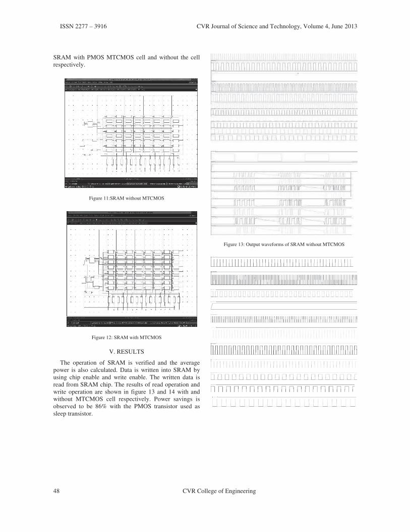
ISSN 2277 – 3916 CVR Journal of Science and Technology, Volume 4, June 2013
48 CVR College of Engineering
SRAM with PMOS MTCMOS cell and without the cell
respectively.
Figure 11:SRAM without MTCMOS
Figure 12: SRAM with MTCMOS
V. RESULTS
The operation of SRAM is verified and the average
power is also calculated. Data is written into SRAM by
using chip enable and write enable. The written data is
read from SRAM chip. The results of read operation and
write operation are shown in figure 13 and 14 with and
without MTCMOS cell respectively. Power savings is
observed to be 86% with the PMOS transistor used as
sleep transistor.
Figure 13: Output waveforms of SRAM without MTCMOS

ISSN 2277 – 3916 CVR Journal of Science and Technology, Volume 4, June 2013
CVR College of Engineering 49
Figure14: Output waveforms of SRAM with MTCMOS
Table1
Comparison of power consumed with and without MTCMOS
S.NO COMPONENT
WITHOUT
MTCMOS
WITH
MTCMOS
1 INVERTER 117.5nW 71.53nW
2 NAND GATE 248.9nw 98.12nW
3 D-LATCH 1.507uW 0.6268uW
4 TRI-STATE
BUFFER 1.216uW 0.801uW
5 3x8 DECODER 9.47uW 2.113uW
6 MEMORY CELL 1.559uW 0.368uW
7 8x8
SRAM 97.92uW 13.11uW
CONCLUSIONS
In this work, SRAM is implemented for minimum
leakage power dissipation with overall 86% of power
savings. The SRAM operating in read mode and write
mode should have "readability" and "write stability"
respectively. SRAM has been verified for reading the
data that is requested and writing the data or updating the
contents. When the sleep enable is not active, SRAM will
be in standby mode. There is tradeoff between area and
power as PMOS takes more space on silicon but with
much better savings in power dissipation.
REFERENCES
[1] Digital Design Principles & Practices- John F. Wakerly,
PHI/ Pearson Education Asia, 3rd Ed., 2005
[2] Essentials of VLSI circuits and systems by Kamran
Eshraghain, Eshraghian Dougles and A. Pucknell, PHI,
2005 Edition
[3] M. Anis, S. Areibi, and M. Elmasry, “Design and
Optimization of Multithreshold CMOS (MTCMOS)
Circuits,” IEEE Transaction on Computer-Aided Design
of Integrated Circuits and Systems,vol. 22, no. 10, pp.
1324- 1342, Oct. 2003.
[4] Cadence, “Cadence Low Power Design Flow” Cadence,
“Low Power Application Note for RC 4.1 and SoCE 4.1
USR3”, Version 1.0,1/14/2005
[5] Digital Logic and Microprocessor Design With VHDL by
Enoch O. Hwang
[6] S. Sirichotiyakul and et al., “Stand-by Power Minimization
through Simultaneous Threshold Voltage Selection and
Circuit Sizing,” Proc. of the DAC, pp. 436-441, 1999.

ISSN 2277 – 3916 CVR Journal of Science and Technology, Volume 4, June 2013
50 CVR College of Engineering
Design of a Portable Functional Electrical
System for Foot Drop Patients Harivardhagini S
1
1CVR College of Engineering, Department of EIE, Ibrahimpatan, R.R.District, A.P., India
Email: [email protected]
Abstract- A portable functional electrical stimulation
system has been designed using embedded systems
technology. The system, which was applied to patients
suffering from foot drop, uses sensors to monitor foot
movement and orientation in a unique way, uses
sophisticated algorithms for feedback, and drives an
array of surface electrodes for stimulation. A new
technique was invented based on using the twitch
response of muscles to optimize the configuration of the
electrode array. This reduces the setup time in the clinic.
The feedback is used from the sensors and the optimum
configuration of electrodes is chosen to produce correct
stimulation and movement in real time. The instrument
presents the patient with a ranked list of electrode
combinations that are likely to be optimum, the patient
can then choose a combination that is both effective and
comfortable. The system can change the pattern of
electrodes and also the stimulation signal during the
process of stimulation. This may enable some problems
associated with fatigue and skin irritation to be reduced.
Trials were carried on 10 controls and 2 patients to test
the instrument and study and develop the system
optimization and control algorithms. These preliminary
clinical trials showed that control of the stimulation
during walking, based on the optimization algorithms
developed in this work, gives high quality correction of
foot drop. This was shown by gait assessment analysis by
the physiotherapists earlier in the project. These trials
prove that the concept of using the electrode array for
stimulation has advantages over using a conventional 2-
electrode system. The system has been designed and
developed for the mentioned problem and has been tested
for its efficacy.
Index Terms— Embedded systems technology, foot drop ,
functional electrical stimulation system
I. INTRODUCTION
When the dropping of the forefoot occurs due to
weakness, damage of the peroneal nerve or paralysis of
the muscles in the anterior portion of the lower leg,
such condition is called FOOT DROP. Though it is not
a disease, it serves as a symptom for a bigger problem.
Foot drop is characterized by the difficulty or the
inability in moving the ankle and toes upward
(dorsiflexion). Foot drop condition, can be temporary
or permanent depending upon the weakness state of the
muscle or paralysis. It can occur unilaterally or
bilaterally. While stepping forward during walking, the
knees are bent slightly so that the front of the foot can
be lifted higher than usual to prevent the foot from
dragging along the ground. Another cause of foot drop
is the nerve damage. Multiple Sclerosis (MS) or Spinal
Cord Injury (SCI) can produce partial or total paralysis.
A person suffering from any one of the above
conditions may not be able to move his or her body
parts. Other factors that may get affected includes
problems in breathing, blood circulation, bladder and
bowel function. Over the last 30 years several methods
and devices are invented by scientists and engineers to
assist these problems. One such technique is called
Functional Electrical Stimulation (FES). Any person
suffering from MS or SCI can try FES as a treatment
option as it can be applied to many different physical
problems.
FES is a method of application of low level
electrical currents to certain body parts to restore or
improve its function. One example of FES system is a
pacemaker. Some other types of FES may help to
restore lost abilities such as standing or grasping. Also,
FES may assist with some secondary problems of
paralysis such as slow wound healing or poor blood
circulation. In such treatments the term used is general
called as Electrical Stimulation or ES. Some drawbacks
of FES systems are found especially with people
having complete spinal lesion, in such cases it provides
benefits only when the system is operating. The
benefits disappear when the system is turned OFF. So
FES is an assistive device. In cases where patients
suffer from incomplete spinal lesion or multiple
sclerosis the usage of FES may help to recall some
amount of voluntary muscle function. In such cases
benefits are present even when the system is turned
OFF. This is a restorative benefit of FES. FES itself
does not reverse paralysis. People of any age or any
level of injury can undergo this technique. This makes
FES technology far more superior than many other
similar techniques.
II. FES TECHNOLOGY
The main components of an FES system are the
electrodes, the stimulator, and sensors or switches.
When FES is being used to move muscles, current

ISSN 2277 – 3916 CVR Journal of Science and Technology, Volume 4, June 2013
CVR College of Engineering 51
pulses in the electrodes cause the weakened or
paralyzed muscles to contract. In other applications,
currents in the electrodes may simply produce
electrical currents in the tissues without moving any
muscles. The stimulator controls the strength and
timing of the low-level pulses that flow to the
electrodes. The sensors or switches control the starting
and stopping of the pulses supplied by the stimulator.
The FES simulator unit is shown in figure 1 and the
parts of it are explained as follows.
Figure 1. FES Simulator unit
A. Electrodes
Skin Surface electrodes may be attached to the skin
daily. Several other types of electrodes are available
that can also be implanted within the body. Skin
surface electrodes are generally made of a flexible
material such as rubber that has the ability to conduct
electricity. Tiny electrical currents are sent through the
electrode to the skin and the tissues beneath the skin.
Generally surface electrodes are attached with a
conductive gel while others are self adhesive. The
electrodes of either type may be reusable. It is
convenient to simply apply electrodes to the skin
surface. Examples are plate electrodes, suction type
electrodes, floating electrodes etc.
B. Leads and Stimulators
Leads are used to connect the electrodes to a
stimulator. The leads are insulated wires. The electrical
charge is delivered to the nerve, muscle or other tissue
through the leads from the simulator. Stimulators
mostly are external units. The size of a stimulator can
be as small as a calculator or as large as a computer
workstation. A stimulator usually has a computer
controller unit built into it. Each stimulation channel
sends pulses to one or more electrodes.
C. Sensors
Sensors are electronic or mechanical devices that
measure some feature of the environment and send
information about it back to the stimulator-controller.
This information is used by the controller to adjust the
stimulation. Sensors may include switches that the FES
user can use to start and stop the system. Also some
systems have switches that allow the user to select
from a menu of choices. Certain sensors are built into
shoes or braces to detect the angle at a joint or the
pressure when weight transfers onto a foot. All the
sensors used are man-made or artificial sensors.
III. HARDWARE MODEL
The basic hardware is divided into two parts
Required Voltage Supplier and the Controller part
A. Required Voltage Supplier
The Required Voltage Supplier is shown in Figure 2
It supplies around 200 Volts to the body surface
electrodes which are used to stimulate the inactive
nerves. It contains the following parts
Astable multi vibrator
Centre tapped transformer
Bridge rectifier
Figure 2. Required Voltage Supplier
An Astable Multivibrator is also known as a FREE-
RUNNING MULTIVIBRATOR. When the time is ON
it alternates between two different output voltage levels
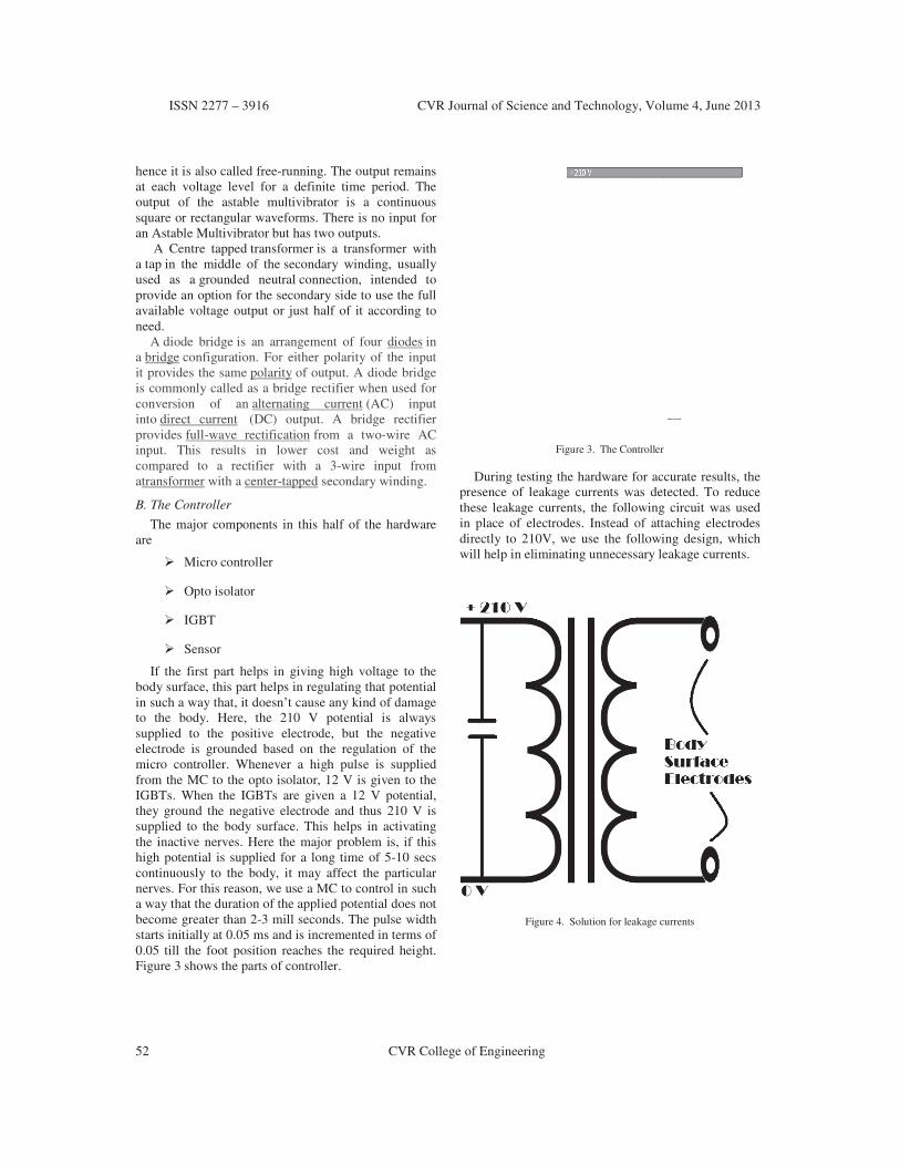
ISSN 2277 – 3916 CVR Journal of Science and Technology, Volume 4, June 2013
52 CVR College of Engineering
hence it is also called free-running. The output remains
at each voltage level for a definite time period. The
output of the astable multivibrator is a continuous
square or rectangular waveforms. There is no input for
an Astable Multivibrator but has two outputs.
A Centre tapped transformer is a transformer with
a tap in the middle of the secondary winding, usually
used as a grounded neutral connection, intended to
provide an option for the secondary side to use the full
available voltage output or just half of it according to
need.
A diode bridge is an arrangement of four diodes in
a bridge configuration. For either polarity of the input
it provides the same polarity of output. A diode bridge
is commonly called as a bridge rectifier when used for
conversion of an alternating current (AC) input
into direct current (DC) output. A bridge rectifier
provides full-wave rectification from a two-wire AC
input. This results in lower cost and weight as
compared to a rectifier with a 3-wire input from
atransformer with a center-tapped secondary winding.
B. The Controller
The major components in this half of the hardware
are
Micro controller
Opto isolator
IGBT
Sensor
If the first part helps in giving high voltage to the
body surface, this part helps in regulating that potential
in such a way that, it doesn’t cause any kind of damage
to the body. Here, the 210 V potential is always
supplied to the positive electrode, but the negative
electrode is grounded based on the regulation of the
micro controller. Whenever a high pulse is supplied
from the MC to the opto isolator, 12 V is given to the
IGBTs. When the IGBTs are given a 12 V potential,
they ground the negative electrode and thus 210 V is
supplied to the body surface. This helps in activating
the inactive nerves. Here the major problem is, if this
high potential is supplied for a long time of 5-10 secs
continuously to the body, it may affect the particular
nerves. For this reason, we use a MC to control in such
a way that the duration of the applied potential does not
become greater than 2-3 mill seconds. The pulse width
starts initially at 0.05 ms and is incremented in terms of
0.05 till the foot position reaches the required height.
Figure 3 shows the parts of controller.
Figure 3. The Controller
During testing the hardware for accurate results, the
presence of leakage currents was detected. To reduce
these leakage currents, the following circuit was used
in place of electrodes. Instead of attaching electrodes
directly to 210V, we use the following design, which
will help in eliminating unnecessary leakage currents.
Figure 4. Solution for leakage currents

ISSN 2277 – 3916 CVR Journal of Science and Technology, Volume 4, June 2013
CVR College of Engineering 53
IV. CONCLUSION
The benefits of FES begin with improved walking:
Provide close to natural movement while
walking
Increase speed and improve steadiness while
walking
Increase social participation
Re-educates the muscles to function without
the need of the system
Prevents loss of muscle
The range of motion in the ankle and foot is
maintained or increased
Increase in local blood flow
V. REFERENCES
[1] Acimovic R, Gros N, Malezic M, Strojnik P, Kljajic M,
Stanic U, and Simic V, “A comparative study of the
functionality of the second generation of peroneal
stimulators”, Proc. 10th RESNA Conf, (PP: 621–623),
1987.
[2] http://feswww.fes.cwru.edu/info/
[3] Alon G, Kantor G, Ho HS, “The effects of selected
stimulus waveforms on pulse and phase characteristics
at sensory and motor thresholds”, Phys Ther, (Vol: 74,
PP: 951-962), 1994.
[4] Brandell H. B. R, “Study and Correction of Human Gait
by Electrical Stimulation”, The American Surgeon,
(Vol:52, No:5), 1986.
[5] ”Biomedical instrumentation and Measurements” by
Leslie Cromwell.
[6] “The Handbook of Biomedical Instrumentation” by R.S
Khandpur, Second Edition.
[7] “Medical Instrumentation” by John Webster, Third
Edition.

ISSN 2277 – 3916 CVR Journal of Science and Technology, Volume 4, June 2013
54 CVR College of Engineering
Low-Power Successive Approximation ADC with
0.5 V Supply for Medical Implantable Devices
O. Venkata Krishna 1
and B. Janardhana Rao 2
1 CVR College of Engineering/EIE, Hyderabad, India
Email: [email protected] 2
CVR College of Engineering/ECE, Hyderabad, India
Email: [email protected]
Abstract- In this paper the design and implementation of
very low-power Analog to Digital converter, which is used in
medical implantable devices like pacemakers et al. The ADC
uses a successive approximation architecture and operates
with a low supply voltage is 0.5 V. A suitable dynamic two-
stage comparator is selected due to its energy efficiency and
capability of working in low supply voltages. This ultra-low
power 10-bit ADC is Implemented in a 90nm
Complimentary Metal-Oxide semiconductor (CMOS)
technology, this ADC consumes 12nW at supply voltage of
0.5V and sampling frequency of 1kS/s with figure of merit
0.14pJ/Conversion. It has a signal-to-noise-and-distortion
(SINAD) ratio of 60.29dB and effective-number-of-bits
(ENOB) of 9.72 bits.
Index terms— Pacemaker, Analog-to-digital conversion,
CMOS, low power, low voltage, two stage dynamic latched
comparator, binary search algorithm for successive
approximation.
I. INTRODUCTION
Successive approximation analog-to-digital
converters have recently become very attractive in low-
power moderate-resolution/ moderate-speed applications
such as implantable bio-medical devices or wireless
sensor nodes due to their minimal active analog circuit
requirements and low power consumption. As an integral
part of the medical implantable devices like the
Pacemaker, a moderate resolution ) with low power
dissipation Analog-to-Digital Converter is
required[1].The converter should also operate from a low
power supply to drive its integration with low-power
digital circuitry. In this paper, we present an analog-to-
digital converter (ADC) that satisfies requirements of
Pacemakers. The Architecture of a Successive
Approximation ADC is shown in Figure.1, It consists of a
sample-and-hold (S/H) circuit, a Comparator, a
Successive Approximation Register (SAR), and a digital-
to- analog converter (DAC). The operation of the
Successive Approximation-ADC starts with the
sampling phase, the analog input signal is sampled by the
S/H circuit and this sample is given to comparator.
During the conversion phase, the SAR and control logic
perform a binary search algorithm, which constructs the
binary word. This binary word is fed through the DAC;
then DAC produced value is an equivalent analog value
which is exactly half of the DAC reference value. This is
compared with the sampled analog input signal by the
comparator. The comparator gives either VDD or Zero, if
VH >VA or VH < VA respectively. The same procedure is
repeated for generating the reference voltage and it is
compared with the sampled value and finally set the
input Digital data for Successive Approximation Register
in N clock cycles. For entire conversion of ADC N+1
clock cycles are required.
This paper proposes a new 10-bit ADC fabricated in
the 90nm CMOS technology. Section II explains about
the proposed SAR individual blocks. Various analyses
about switching power and Implementation results are
presented in section III. Finally, section VI draws our
conclusions.
II. ARCHITECTURE DESIGN
The architecture of Successive approximation
Analogto-Digital converter is shown in Figure 2. It
mainly consists of Sample & hold circuit, Comparator,
digital to analog converter and successive approximation
register.
Figure 1. The Architecture of A Successive Approximation ADC.
A. Sampling Network Design
The Sampler takes the varying input Analog signal and
converts it to a fixed voltage or current or electrical
charge. The signal is sampled at Nyquist rate i.e. a
frequency rate more than double the maximum
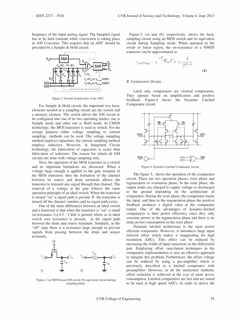
ISSN 2277 – 3916 CVR Journal of Science and Technology, Volume 4, June 2013
CVR College of Engineering 55
frequency of the input analog signal. The Sampled signal
has to be held constant while conversion is taking place
in A/D Converter. This requires that an ADC should be
preceded by a Sample & Hold circuit.
Figure 2. Overall Architecture of the ADC .
For Sample & Hold circuit, the important two basic
elements needed in a sampling circuit are the switch and
a memory element. The switch allows the S/H circuit to
be configured into one of its two operating modes: one is
Sample mode and other one is Hold mode. In CMOS
technology, the MOS transistor is used as switch. For the
storage purpose either voltage sampling or current
sampling methods can be used. The voltage sampling
method employs capacitors; the current sampling method
employs inductors. However, in Integrated Circuit
technology, the fabrication of capacitors is easier than
fabrication of inductors. The reason for which all S/H
circuits are done with voltage sampling only.
Next, the operation of the MOS transistor as a switch
and its important limitations are discussed. When a
voltage large enough is applied to the gate terminal of
the MOS transistor, then the formation of the channel
between its source and drain terminals allows the
transistor to transmit any signal through that channel. The
removal of a voltage at the gate follows the same
operation principle of an ideal switch. When the transistor
is turned “on” a signal path is present. If the transistor is
turned off the channel vanishes and no signal path exists.
One of the main differences between an ideal switch
and a transistor is that when the transistor is “on”, a small
on-resistance (i.e.0.5 - 2 k ) is present where as in ideal
switch zero resistance is present, in the signal path
between the drain and source terminals. Similarly, in the
“off” state there is a resistance large enough to prevent
signals from passing between the drain and source
terminals.
Figure. 3 (a) MOS-based S/H circuit (b) equivalent circuit during
sampling phase.
Figure.3. (a) and (b), respectively, shows the basic
sampling circuit using an MOS switch and its equivalent
circuit during Sampling mode. When operated in the
triode or linear region, the on-resistance of a NMOS
transistor can be approximated as
(1)
B. Comparator Design
Latch only comparators are clocked comparators.
They operate based on amplification and positive
feedback. Figure.4 shows the Dynamic Latched
Comparator circuit.
Figure 4. Dynamic-Latched Comparator circuit.
The figure 5. shows the operation of the comparator
circuit. There are two operation phases, reset phase and
regeneration or evaluation phase. In the reset phase, the
output nodes are charged to supply voltage or discharged
to the ground depending on the architecture of
comparator. During the reset phase, the comparator tracks
the input, and then in the regeneration phase the positive
feedback produces a digital value at the comparator
output. One of the advantages of dynamic-latched
comparators is their power efficiency since they only
consume power in the regeneration phase and there is no
static power consumption in the reset phase. Dynamic latched architecture is the most power
efficient comparator. However, it introduces large input
referred offset which makes it unappealing for high
resolution ADCs. This effect can be reduced by
increasing the width of input transistors in the differential
pair. Employing offset cancelation techniques in the
comparator implementation is also an effective approach
to mitigate this problem. Furthermore, the offset voltage
can be reduced by using a pre-amplifier which is
previously described as a latched comparator with
preamplifier. However, in all the mentioned methods,
offset reduction is achieved at the cost of more power
consumption. Latched comparators are fast and are suited
to be used in high speed ADCs. In order to derive the
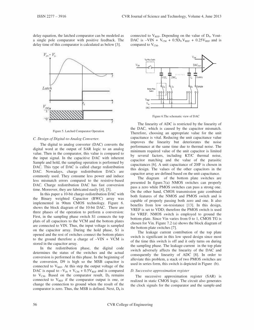
ISSN 2277 – 3916 CVR Journal of Science and Technology, Volume 4, June 2013
56 CVR College of Engineering
delay equation, the latched comparator can be modeled as
a single pole comparator with positive feedback. The
delay time of this comparator is calculated as below [3].
Figure 5. Latched Comparator Operation
C. Design of Digital-to-Analog Converter.
The digital to analog converter (DAC) converts the
digital word at the output of SAR logic to an analog
value. Then in the comparator, this value is compared to
the input signal. In the capacitive DAC with inherent
Sample and hold, the sampling operation is performed by
DAC. This type of DAC is called charge redistribution
DAC. Nowadays, charge redistribution DACs are
commonly used. They consume less power and induce
less mismatch errors compared to the resistive-based
DAC. Charge redistribution DAC has fast conversion
time. Moreover, they are fabricated easily [4], [5].
In this paper a 10-bit charge-redistribution DAC with
the Binary weighted Capacitor (BWC) array was
implemented in 90nm CMOS technology. Figure 6.
shows the block diagram of the 10-bit DAC. There are
three phases of the operation to perform a conversion:
First, in the sampling phase switch S1 connects the top
plats of all capacitors to the VCM and the bottom plates
are connected to VIN. Thus, the input voltage is sampled
on the capacitor array. During the hold phase, S1 is
opened and the rest of switches connect the bottom plates
to the ground therefore a charge of –VIN + VCM is
stored in the capacitor array.
In the redistribution phase, the digital code
determines the status of the switches and the actual
conversion is performed in this phase. In the beginning of
the conversion, D9 is high so the MSB capacitor is
connected to VREF. At this step the output voltage of the
DAC is equal to –VIN + VCM + 0.5VREF and is compared
to VCM. Based on the comparator result, D9 remains
connected to VREF if the comparator output is one, or
change the connection to ground when the result of the
comparator is zero. Thus, the MSB is defined. Next, D8 is
connected to VREF. Depending on the value of D9, Vout-
DAC is –VIN + VCM + 0.5D9.VREF + 0.25VREF and is
compared to VCM.
Figure 6.The schematic view of DAC
The linearity of ADC is restricted by the linearity of
the DAC, which is caused by the capacitor mismatch.
Therefore, choosing an appropriate value for the unit
capacitance is vital. Reducing the unit capacitance value
improves the linearity but deteriorates the noise
performance at the same time due to thermal noise. The
minimum required value of the unit capacitor is limited
by several factors, including KT/C thermal noise,
capacitor matching and the value of the parasitic
capacitances [6]. A unit capacitance of 20fF is chosen in
this design. The values of the other capacitors in the
capacitor array are defined based on the unit capacitance.
The diagram of the bottom plate switches are
presented In figure.7(a) NMOS switches can properly
pass a zero while PMOS switches can pass a strong one.
On the other hand, CMOS transmission gate combined
both features of the NMOS and PMOS switch and is
capable of properly passing both zero and one. It also
benefits from low on-resistance [13]. In this design,
VREF is set to VDD; therefore the PMOS switch is used
for VREF. NMOS switch is employed to ground the
bottom plate. Since Vin varies from 0 to 1, CMOS TG is
chosen for Vin. Figure 7.2 (a) shows the block diagram of
the bottom plate switches [7].
The leakage current contribution of the top plate
switch is significant in this low speed design since most
of the time this switch is off and it only turns on during
the sampling phase. The leakage-current in the top plate
switch adversely affects the linearity of the DAC and
consequently the linearity of ADC [8]. In order to
alleviate this problem, a stack of two PMOS switches are
used in series form, this switch is depicted in Figure (b).
D. Successive approximation register
The successive approximation register (SAR) is
realized in static CMOS logic. The circuit also generates
the clock signals for the comparator and the sample-and

ISSN 2277 – 3916 CVR Journal of Science and Technology, Volume 4, June 2013
CVR College of Engineering 57
hold circuit. All clock signals are derived from an
externally provided master clock.
(b)
Figure 7.Schematic views of a) bottom plate switch and b) top plate
switch.
Successive approximation register ADC implements
the binary search algorithm using SAR digital control
logic. In general, there are two fundamentally different
approaches to designing the SAR logic. The first one is
proposed by Anderson consists of a ring counter and a
shift register. At least 2N Flip-flops are employed in this
kind of SAR [9]. The other, which is proposed by Rossi,
contains N flip flops and some combinational logic [10].
The SAR control logic determines the value of bits
sequentially based on the result of the comparator. Each
conversion takes 12 clock cycles. In the first clock cycle,
SAR is in the reset mode and all the remaining outputs
are zero. In the next ten clock cycles, data is converted
and each bit is determined sequentially. The last cycle is
for storing the results of the complete conversion.
The SAR architecture shown in Figure 8. is presented
in [9], and is commonly used in SAR ADCs due to its
straightforward design technique. This control logic
encompasses a ring counter and a code register. The ring
counter is in fact a shift register. For each conversion, in
clock cycle 0, the EOC signal is high and all Flip Flops
outputs reset to zero, and for the rest of cycles EOC is
low. In the next clock cycle, the most significant Flip
Flop is set to one which corresponds to MSB of the
digital word to DAC. Then the counter shifts ‘1’ through
the Flip-Flops from MSB to LSB. In each clock cycle, one of the outputs in the ring
counter sets a Flip-Flop in the code register. The output
of this Flip-Flop, which is set by the ring counter is used
as the clock signal for the previous Flip Flop. At rising
edge of the clock, this Flip-Flop loads the result from the
comparator. This type of SAR logic requires 12 clock
cycles to convert each sample.
Figure 8. The SAR block diagram
The Flip-Flops which are employed in this structure
are set-reset D-FFs. For the low power purpose,
transmission gate based Flip Flops are used [11].
Minimum size transistors with double length are chosen
for improving the power performance. In order to
decrease the leakage power even more while
simultaneously maintaining the speed, high threshold
voltage transistors are used in the non- critical paths and
low-VT transistors in the critical path. Thus, this dual
threshold approach provides high performance Flip-Flops
[12].
III. SIMULATION RESULTS
The Low power 10-bit ADC is fabricated in a 90nm n-
well CMOS process technology with single poly, four
metal layers and a MIMCAP (Metal-Insulator-Metal)
capacitor option. The threshold voltages are 0.43V for the
n-MOS and -0.38V for the p-MOS device. Simulation
results for the low supply voltage as well as high
temperature are presented to evaluate their influence on
power consumption.
The ADC is simulated with VDD= VREF = 1,VCM =
0.5V, and sampling frequency of 1kS/s. The input signal
is an full swing sinusoidal with fin= 450Hz. The
simulation results under 27ºC and 80ºC temperatures are
presented in the Table 1.
The total power consumption of the implemented SAR
ADC, including the clock power is almost 12.4nW. The
distribution of power consumption between different
blocks of ADC is shown in figure 9.
As shown in the Figure 9, DAC consumes the largest
amount of power among other blocks which is 84%. As
discussed above, the unit capacitance in the DAC is
chosen to be 20fF. After DAC, SAR control logic with
12%, clock power and comparator both with 2%
consumes the largest amount of power respectively.
A. Dynamic Performance Evaluation
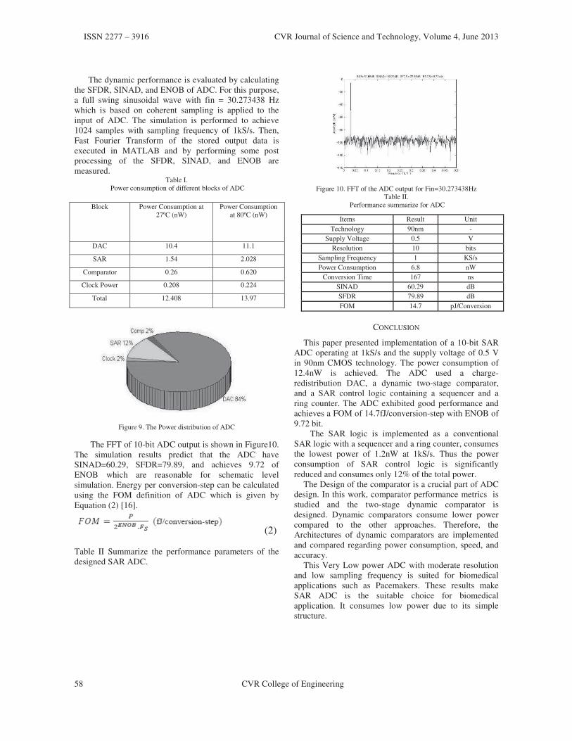
ISSN 2277 – 3916 CVR Journal of Science and Technology, Volume 4, June 2013
58 CVR College of Engineering
The dynamic performance is evaluated by calculating
the SFDR, SINAD, and ENOB of ADC. For this purpose,
a full swing sinusoidal wave with fin = 30.273438 Hz
which is based on coherent sampling is applied to the
input of ADC. The simulation is performed to achieve
1024 samples with sampling frequency of 1kS/s. Then,
Fast Fourier Transform of the stored output data is
executed in MATLAB and by performing some post
processing of the SFDR, SINAD, and ENOB are
measured. Table I.
Power consumption of different blocks of ADC
Block Power Consumption at
27ºC (nW)
Power Consumption
at 80ºC (nW)
DAC 10.4 11.1
SAR 1.54 2.028
Comparator 0.26 0.620
Clock Power 0.208 0.224
Total 12.408 13.97
Figure 9. The Power distribution of ADC
The FFT of 10-bit ADC output is shown in Figure10.
The simulation results predict that the ADC have
SINAD=60.29, SFDR=79.89, and achieves 9.72 of
ENOB which are reasonable for schematic level
simulation. Energy per conversion-step can be calculated
using the FOM definition of ADC which is given by
Equation (2) [16].
(2)
Table II Summarize the performance parameters of the
designed SAR ADC.
Figure 10. FFT of the ADC output for Fin=30.273438Hz
Table II.
Performance summarize for ADC
CONCLUSION
This paper presented implementation of a 10-bit SAR
ADC operating at 1kS/s and the supply voltage of 0.5 V
in 90nm CMOS technology. The power consumption of
12.4nW is achieved. The ADC used a charge-
redistribution DAC, a dynamic two-stage comparator,
and a SAR control logic containing a sequencer and a
ring counter. The ADC exhibited good performance and
achieves a FOM of 14.7fJ/conversion-step with ENOB of
9.72 bit.
The SAR logic is implemented as a conventional
SAR logic with a sequencer and a ring counter, consumes
the lowest power of 1.2nW at 1kS/s. Thus the power
consumption of SAR control logic is significantly
reduced and consumes only 12% of the total power.
The Design of the comparator is a crucial part of ADC
design. In this work, comparator performance metrics is
studied and the two-stage dynamic comparator is
designed. Dynamic comparators consume lower power
compared to the other approaches. Therefore, the
Architectures of dynamic comparators are implemented
and compared regarding power consumption, speed, and
accuracy.
This Very Low power ADC with moderate resolution
and low sampling frequency is suited for biomedical
applications such as Pacemakers. These results make
SAR ADC is the suitable choice for biomedical
application. It consumes low power due to its simple
structure.
Items Result Unit
Technology 90nm -
Supply Voltage 0.5 V
Resolution 10 bits
Sampling Frequency 1 KS/s
Power Consumption 6.8 nW
Conversion Time 167 ns
SINAD 60.29 dB
SFDR 79.89 dB
FOM 14.7 pJ/Conversion
ISSN 2277 – 3916 CVR Journal of Science and Technology, Volume 4, June 2013
CVR College of Engineering 59
REFERENCES
[1] Dai Zhang,” Design and Evaluation of an Ultra-Low Power
Successive Approximation ADC “, LiTH-ISY-EX--
09/4176—SE, March 2009.
[2] J. Sauerbrey, D. Schmitt-Landsiedel, and R. Thewes, “A
0.5-v 1-µW Successive Approximation ADC,” IEEE
Journal of Solid-State Circuits, vol. 38, no. 7, July 2003
[3] H. Khurramabadi ADC Converters (Lecture 21). UC
Berkeley Course, Analog-Digital Interfaces in VLSI
Technology EE247. 2006
[4] B. Razavi, Principles of Data Conversion System Design,
IEEE Press, 1995.
[5] J. L. McCreary and P. R. Gray, “All-MOS Charge
Redistribution Analog-to-Digital Conversion Techniques-
Part I,” IEEE Journal of Solid-State Circuits, vol. SC-10,
no. 6, December 1975.
[6] M. Saberi, R. Lotfi, K. Mafinezhad, W. A. Serdijn,
“Analysis of Power Consumption and Lineary in
Capacitive Digital-to-Analog Converters Used in
Successive Approximation ADCs,” IEEE Transactions on
Circuits and Systems, vol. 58, no. 8, August 2011.
[7] D. Zhang, “Design and Evaluation of an Ultra-Low Power
Successive Approximation ADC,” Master thesis,
Linkoping University, 2009.
[8] A. K. Bhide, D. Zhang and A. Alvandpour, “Design of
CMOS Sampling Switch for Ultra-Low Power ADCs in
Biomedical Application,” in proceedings of the 28th
Norchip conference IEEE,Nov.2010.
[9] T.O. Anderson, “Optimum Control Logic for Successive
Approximation Analog-to-Digital Converters,” Computer
Design, vol. 11, no. 7, pp. 81-86, 1972.
[10] A. Rossi and G. Fucili, “Nonredundant successive
approximation register for A/D converter,” Electronics
Letters, vol.32, no.12, pp.1055-1057,1996
[11] S. T. Oskuii, “Comparative Study on Low-Power High-
Performance Flip-Flops,” Master thesis, Linkoping
University, 2003.
[12] Joao C. Vital andPedro M. Figueiredo, “Kickback Noise
Reduction Techniques for CMOS Latched Comparators,”
IEEE Transactions on Circuits and Systems, vol.53, no.7,
July 2006.
[13] J. M Rabaey, A. Chandrakasan , and B. Nikolic, Digital
Integrated Circuits – A Desigsn Perspective, Prentice Hall,
2nd edition, 2003.

ISSN 2277 – 3916 CVR Journal of Science and Technology, Volume 4, June 2013
60 CVR College of Engineering
PC Based Wave Form Generator Using
Labview Mahammad D V
1, Dr B V S Goud
1 and Dr D Linga Reddy
2
1Dept. of Electronics & Instrumentation Tech. Acharya Nagarjuna Uni., Nagarjuna Nagar – 522510, A.P. India.
E mail : [email protected] 2CVR College of Engineering, Vastunagar, Mangalpalli (V), Ibrahimpatnam (M), R R Dist., 501 510, A P India.
E mail : [email protected]
Abstract--A Personal Computer (PC) based wave form
generator for laboratory applications has been thought and
developed which is generating Sine, Square and Triangular
waves in the range of 1 Hz to 20 MHz. The generation,
recording and monitoring of wave forms, controlled through
USB Data Acquisition system (DAS) connected to computer
which is having 14-bit ADC, 10-bit DAC and 12-I/O lines. In
the present work National Instrument’s USB DAS 6009,
Maxim Company’s Max038 waveform generator are used
for Hardware development. Higher level Graphical
language such as ‘LabVIEW’ is used to develop the
software. The experimental study reveals that the
developed system is quite suitable to perform laboratory
applications accurately. The results obtained from system
are in agreement with results of standard instruments.
Index Terms-- Wave Form, LabVIEW, DAS, FLC.
I. INTRODUCTION
A Waveform generator is widely used for experimental
work in all electronics labs [1,2,3]. It generates various
types of wave forms like sine, square, triangle, etc., with
a particular frequency, amplitude and duty-cycle.
Currently, most waveform generators in the laboratory
made use of manual control and these are not
programmable. Usually, the manual function generators
do not provide feedback to the user regarding the
condition of the output. Therefore, the user will never
know whether the required waveform is available at the
output or not unless they measure it by suitable
equipment. Although software controlled waveform
generators are available in the market, they are not widely
used, because of their high cost. To overcome this
problem, A Low cost PC based wave form generator for
laboratory application has been thought and developed in
our lab. This is generating sine, square and triangle wave
forms in the range from 1Hz to 20 MHz. The present
work deal with designing and building a programmable
waveform generator in LabVIEW plot form. The block
diagram of the system is shown in figure-1.
Figure 1. Block diagram of PC based waveform generator system.
II THE DESIGN OF PC BASED WAVEFORM
GENERATOR
A. Personal Computer
Computer plays a pivotal role in
instrumentation in field of data acquisition;
instrument control and data processing [4]. To
measure and control any instrument it is to be
interfaced with a personal computer. For this we
need interface ports like Serial, Parallel and
Universal Serial Bus (USB) ports. In present
study, a powerful 32-bit Intel® core™2 Duo CPU
processor based Acer personal computer is used.
It consists of a system unit of CPU, clock speed
2.80 GHz, 360 GB hard disk, internal memory
2GB RAM, 105 key-full function keyboard and
color monitor. The mother board consists of two
PCI slots, four USB ports, two serial and one
parallel ports to interface Data Acquisition
Systems (DAS). The system is compatible to
Windows-7, Unix Operating System and Linux
OS etc. also compatible to a vast variety of
popular application PC software packages and all
language compilers. However, the software and
the interface are designed such that it can work in
any advanced computer environment.
B. NI DAS USB-6009
To measure and control the hardware
frequency of the output of Max-038 function
generator, it is to be interfaced with a PC. It
requires one ADC Input channel, one DAC output
channel, four I/O lines. The DIOT/DAS card
provides these requirements. In present study,
DAS of National instruments USB-6009 is used.
It is having 14-bit ADC with 8-single ended or 4-
dual ended channels, two 10-bit DAC channels,
12-I/O lines and two counter/timers [5]. This
fulfils the present system requirements.

ISSN 2277 – 3916 CVR Journal of Science and Technology, Volume 4, June 2013
CVR College of Engineering 61
C. Max038 Waveform Generator IC
Advancement in Integrated Chip technology brings
tremendous changes in simplification of hardware design.
Single chip incorporating much integration of required
tasks. Maxim has produced a family of high quality and
reliable one-chip waveform generator ICs. The IC MAX-
038 is one best among them [6], with accurate, high
frequency, precision function generator producing
triangle, sine, square, and pulse waveforms with a
minimum of external components. It generates 0.1Hz to
20 MHz range of Independent frequency and Duty-Cycle
adjustments with 15% to 85% Variable Duty Cycle.. are
some of the important features. It is a 20-pin IC, works
with +5V supply and features a parallel digital interface
that connects easily to most systems like
Microprocessors/microcontrollers or PCs.
The desired output wave form is selected under logic
control by setting the appropriate code at the A0 and A1
inputs. The wave form selection table is shown in table-1.
The basic oscillator is a relaxation type. The operates by
alternately charging and discharging a capacitor, ‘CF’
with constant current, simultaneously producing a
triangle wave and a square wave.
TABLE 1.
Waveform Selection
A0 A1 Waveform
X 1 Sine wave
0 0 Square wave
1 0 Triangle wave
D. BB PGA103
The PGA 103 is a Programmable gain amplifier having
gains of 1, 10 and 100 which are digitally selected by
two compatible inputs. It is high speed circuitry provides
fast settling time. It operating voltage is +/_ 4v to
+/_18v, available in 8 pin DIP package [7]. The digital
inputs, A0 and A1, select the gain according to the logic
table, table-2. TABLE 2.
PGA103 gain selection
Gain A1 A0
1 0 0
10 0 1
100 1 0
Not valid 1 1
.
E. Interface Circuit
The Max-038 IC’s I/O can easily be interfaced with a
PC. IIN pin is connected to DAC output.. A0, A1 pins
are connected to P0.0, P0.1 port lines of DAS. Frequency
adjustment is accomplished with a capacitor C2 and
variable resistor, R1. I in current is drive from DAS’s
DAC. Amplitude, offset, and duty-cycle adjustments are
performed via variable resistors. Switches A0 and A1
select the waveform type, to be generated. The frequency
range decides the capacitor C2 value (in present work C2
is fixed for particular range). The Fadj pin of U1
is tied to ground through a 12k resistor, so the
frequency of the waveform at U1-19 is f =
2(IIN/C2), where IIN = VREF/R, and VREF =
2.5 V. The output at U1-19 is 2 V p-p, centred
around zero, for all waveforms. For amplitude
adjustment, The portion of U1-19 fed to the
programmable gain amplifier BB PGA103. The
gain varies from 1, 10 and 100 times in fixed 3 -
steps. This gain is digitally selected from PGA’s
Figure 2. Schematic Diagram of PC Based Waveform
Generator.
A0, A1 pins which are connected to P0.2, P0.3
port line of DAS. The duty cycle adjustment is
fixed at 50% in present work for constant output.
The schematic diagram is in figure-2.
F. Software requirement
Software plays very important role in any PC
based instrumentation system, as it includes all
tools which a developer needs to build and
execute applications. In the present work National
Instruments’ LabVIEW 8.5 version is used for
development of application software like C/C++,
Java. It is Graphical programming language, so
called ‘G’ language [8]. It has back panel where
we write programming code in form of icons and
front panel indicators, controls for display and
control purpose. The programs written in
LabVIEW are called “Virtual Instruments” or
VI’s due to their instrument related origin. The
programs created are portable of the type of
machine and operating system. It has a built-in
mathematical function, graphical data display
objects and data input objects. LabVIEW has
many features some them are.. data flow
controlled execution, real time debugging
features, data base (SQL) interfacing for
industrial PLC’s, and add-on software packages
for specific extension of the program features, etc.
The software control program is written in
LabVIEW 8.5.

ISSN 2277 – 3916 CVR Journal of Science and Technology, Volume 4, June 2013
62 CVR College of Engineering
Figure-3a shows the program of front and back panels of
present developed setup system.
Figure 3a. Show a front and back panel of waveform generator in
LabVIEW.
Figure 3b. LabVIEW Program for PC based waveform generator.
III. EXPERIMENTAL
The prototype of the PC based waveform generator is
successfully designed and tested in the laboratory. The
photograph in figure-3 b, shows the prototype used in the
present experiment. The performance of the present
design system is evaluated by comparing with standard
reported instrument [9]. The response time (τ) of
Ferroelectric Liquid Crystal (FLC) compounds
2CI.BAAP.120-BBP and 2CI.BAAP.180-BBP, with
temperature variation is calculated in present work. To
determine the response times (in SC* phase) also by the
measurement of shift (frequency dependent) of the peaks
due to polarization reversal in the current signal
(converted in to voltage) as reported [10] by Bawa et.al. .
Plotting the current peaks measured at double the
frequencies (viz., 100Hz and 200Hz) reduces the pulse
gaps to half in the time axis 10. The scanning time of the
oscilloscope is to be halved, while plotting the higher
frequency signal (to obtain the same abscissa length) and
the slope of the applied triangular pulse. By doing so
(i.e., doubling the frequency), one actually shifts the
event (occurrence of peak of the polarization reversal
current) by the same time corresponds to the response
time of the device. The response time is directly
measured by the difference of the occurrence of peaks in
lower frequency (i.e., 100Hz) time scale. The reported
values are tabulated in table-3. Then the experiment (for
two compounds) is performed by substituting the
function generator with developed waveform generator
and the calculated values are tabulated in the same table.
IV. RESULTS AND DISCUSSION
The temperature variation of response time is
measured by following the reported double
frequency technique [10]. The observed variation
of switching times with temperature in Smectic-
C* phase is given in Tables-3,4,5,6 for the
compounds 2Cl.BAAP.12O-BBP and
2Cl.BAAP.18O-BBP respectively. It is also
observed that the range of switching times
exhibited by the present compounds with
developed setup are found to agree with the
reported [9] values of same FLC compounds.
TABLE 3.
Response time of FLC compound 2CI.BAAP.120-BBP
Table 4
Response time of FLC compound 2CI.BAAP.120-BBP
TABLE 5
Response time of FLC compound 2CI.BAAP.180- BBP
S.No. Temperature
oC
Reported
values (T/µs)
Instrument
measured values
(T/µs)
1 32 90 90
2 33 90 89
3 34 88 87
4 35 78 78
5 36 75 75
6 37 71 70
7 38 66 66
8 39 60 61
9 40 57 57
10 41 49 48
11 42 38 36
12 43 33 30
13 44 22 21
S.No. Temperatureo/C
Reported
values
(T/µs)
Instrument
measured
values(T/µs)
1 35 77 77
2 36 74 75
3 37 71 71
4 38 69 70
5 39 67 67
6 40 65 64
7 41 63 62
8 42 60 60
9 43 58 58
10 44 55 54
11 45 53 53
12 46 48 48
13 47 45 45
14 48 40 42
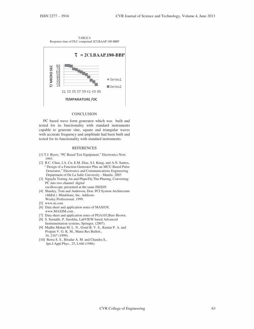
ISSN 2277 – 3916 CVR Journal of Science and Technology, Volume 4, June 2013
CVR College of Engineering 63
TABLE 6
Response time of FLC compound 2CI.BAAP.180-BBP
CONCLUSION
PC based wave form generator which was built and
tested for its functionality with standard instruments
capable to generate sine, square and triangular waves
with accurate frequency and amplitude had been built and
tested for its functionality with standard instruments.
REFERENCES
[1] T.J. Byers, “PC Based Test Equipment,” Electronics Now.
1993.
[2] R.C. Chua, J.A. Cu, E.M. Diaz, S.I. Kung, and A.N. Santos,
“ Design of a Function Generator Plus an MCU-Based Pulse
Generator,” Electronics and Communications Engineering
Department of De La Salle University - Manila. 2003
[3] Nguy n Tr ng An and Ph mTh Thu Ph ng, Converting
PC into two channel digital
oscilloscope, presented at the same ISEE05.
[4] Shanley, Tom and Anderson, Don. PCI System Architecture
(4thEd.). Mindshare, Inc. Addison-
Wesley Professional. 1999.
[5] www.ni.com
[6] Data sheet and application notes of MAX038,
www.MAXIM.com .
[7] Data sheet and application notes of PGA103,Burr-Brown.
[8] S. Sumathi, P. Surekha, LabVIEW based Advanced
Instrumentation systems, Springer, (2007).
[9] Madhu Mohan M. L. N., Goud B. V. S., Kumar P. A. and
Pisipati V. G. K. M., Mater.Res.Bullett.,
34, 2167 (1999).
[10] Bawa S. S., Biradar A. M. and Chandra S.,
Jpn.J.Appl.Phys., 25, L446 (1986).

ISSN 2277 – 3916 CVR Journal of Science and Technology, Volume 4, June 2013
64 CVR College of Engineering
A Simple Laboratory Demonstrate Pacemaker Mahammad D V
1, Dr B.V.S. Goud
1 and Dr D Linga Reddy
2
1Dept. of Electronics & Instrumentation Tech. Acharya Nagarjuna Uni., Nagarjuna Nagar – 522510, A.P. India.
E mail : [email protected] 2CVR College of Engineering, Vastunagar, Mangalpalli (V), Ibrahimpatnam (M), R R Dist., 501 510, A P India.
E mail : [email protected]
Abstract--A simple pacemaker circuit has been designed,
fabricated and tested. The circuit consists of Signal
Generator, Amplifier, Filters and Noise reduction circuits.
The pulse signals generated from an operational amplifier
circuit and fed to monostable 555 timer circuit. The pulses
are acquired with Digital Storage Oscilloscope (DSO). The
performance of the developed system is evaluated by
recording the pulses of people having different heart beats,
wave forms recorded are compared with standard pulse
wave forms e.g. frequency, amplitude, pulse duration, shape
etc. The accuracy of the diagnosis presently depends on the
expertise of the physician.
Index Terms-- Pacemaker, Monostable, Pulse duration.
I. INTRODUCTION
Picture 1(a) 1(b) Pacemaker model.
A pacemaker is a device that placed in chest or
abdomen to help abnormal heart rhythms. This device
uses electronic pulse to promote the heart beat at a
normal rate. In 1958, Arne Larsson became the first to
receive an implantable pacemaker [1,2]. He had a total of
26 devices during his life and campaigned for other
patients needing Pacemaker In 1899, J A McWilliams
reported in the British Medical Journal of his
experiments in which application of an electrical
impulse to the human heart in a systole caused a
ventricular contraction and that a heart rhythm of
60-70 beats per minute could be evoked by
impulses applied at pacing equal to 60–70/minute.
Picture-1a,1b shows the pace maker model.
A. Need of Pacemaker
Doctors recommend pacemaker for a number
of reason. The most common reason is
bradycardia and heart block. BRADYCARDIA is
a slower than normal heart beat. HERT BLOCK
is problem with hearts electrical system. The
disorder occurs when an electrical signal is
slowed or disrupted as it moves through the beat
[3]. Heart block can happen as a result of aging
damage to heart from heart attack or other
condition that interface with heart electrical
activity. Certain nerve and muscle disorder can
also cause heart block, including muscular
dystrophy. Aging or heart disease damages your
sinus node’s ability to set the correct pace for
your heart beat. Such damage can cause slower
than normal heart beat or long pause between
heart beats. The damage also can cause your heart
to alternate between slow and fast rhythms. This
condition is called “sick sinus syndrome”. You
have had a medical procedure to treat an
arrhythmia called atrial fibrillation. A pacemaker
can help regulate your heart beat too much. You
faint or have some other symptoms of a slow
heartbeat. You have heart muscle problem that
causes electrical signal to travel too slowly
through your heart beat muscle. You have long
QT syndrome which puts you at risk for
dangerous arrhythmias.
B. Energy Requirement to Excite Heart Muscle
To overcome of these all some of the measures
are taken like all muscles tissues. The heart can
be simulated with an electric shock. The
minimum energy required for excite the heart
muscle is about 10 µj. For safety purpose, a
pulse of energy 100 µj is applied on heart muscle.
A pulse of 5V, 10mA and 2mS duration is used

ISSN 2277 – 3916 CVR Journal of Science and Technology, Volume 4, June 2013
CVR College of Engineering 65
[4]. Ventricular fibrillation is a dangerous condition. This
occurs due to a too high pulse. A patient loses
consciousness in 10 to 15 sec and the brain cell dead
within a few minutes from oxygen deficiency in the
brain. This is caused by pulse of 400 µj. These pulses
should have the pulse to the ratio of 1:1000 and that
should be negatively going pulse to avoid ionization of
the muscle. Pulse voltage is allowed to adjust in such a
way that the energy is delivered by the pacemaker to the
heart during each pulse. The pulse rate is 70 pulse/min
but many pacemakers are adjusted in the range of 50 to
150 pulse/min. The duration of each pulse is between 1 to
2 ms, shown in figure-1.
Figure 1. Duration of each pulse of Pacemaker.
II. METHODS OF SIMULATION
There are two types of simulations or pacing [3]
• External simulation
• Internal simulation
A. External Simulation
This simulation is used to restart the normal rhythm of
heart. In this case the cardiac stands still. This occur
during open heart surgery or whenever there is sudden
physical shocks or accidents. The paddle shaped
electrode is applied on the surface of the chest and
current of 20 to 150 mA are employed. Picture-2a, 2b
shows the model of external simulation.
Pictures 2(a), 2(b). The model of external simulation of Pacemaker
model.
B. Internal Simulation
This simulation is employed in case where
long term pacing is required because of
permanent damage. The electrodes are in the form
of fine wires coated with Teflon coated stainless
steel. During restarting heart after open heart
surgery a spoon like electrode is used with current
range of 2 to 15 mA.
C. Different Types of Pacemakers
Based on modes of operation of pacemaker is
divided into five types
• Ventricular Asynchronous
Pacemaker (Fixed rate pacemaker)
• Ventricular synchronous pacemaker
• Ventricular Inhibited Pacemaker
(Demand Pacemaker)
• Atrial synchronous Pacemaker
• Atrial Sequential ventricular
inhibited Pacemaker
III. VENTRICULAR ASYNCHRONOUS
PACEMAKER
66
Pacemaker Insertion
Picture 3. Shows pacemaker insertion model
It is the first type of pacing can be used in
atrium or ventricle. It has a simplest mechanism
and longest battery life. It is so cheap and easy to
check and least sensitive device to outside
interference. This pacemaker is suitable for
patient with a stable, total Atrioventricular (AV)
block, a slow rate atrial rate or arterial
arrhythmia. It is basically a simple astable
multivibrator .this produces a stimulus at a fixed
rate irrespective of behaviour of heart rhytms. It is
possible that such an event can be dangerous
because if pacemaker impulse reaches heart
during a certain vulnerable period, the ventricular
fibrillation may occur. Picture-3 shows
pacemaker insertion model.

ISSN 2277 – 3916 CVR Journal of Science and Technology, Volume 4, June 2013
66 CVR College of Engineering
A. Block Diagram of Pacemaker
Figure 2. Block diagram of asynchronous pacemaker.
• Power supply – provides energy
• Oscillator – controls pulse rate
• Pulse output – produces stimuli
• Lead wires – conduct stimuli
• Electrodes – transmit stimuli to the
tissue
Output circuit produces the electrical stimuli to be
applied to the heart [4]. Stimulus generation is triggered
by the timing circuit. Constant voltage pulses typically
rated at 5.0 to 5.5V for 500 to 600µs Constant current
pulses typically rated at 8 to 10mA for 1.0 to 1.2ms.
Asynchronous pacing rates 70 to 90 beats per min.
Figure-3 Realistic depiction of waveform appearing
across heart emitted from capacitor discharge output
circuit.
Figure 3. The Ideal and Realistic waveforms of O/P of pacemaker.
B. Schematic diagram
Figure 4. The schematic diagram of pacemaker
Figure-4 shows the schematic diagram of
pacemaker. It consist of an integrated chip (IC)
741 and IC 555 timer. IC 741 acts as a square
wave generator which generates square wave and
its square wave o/p is fed to as trigger of 555
timer than IC 555 timer produce the required
pulse width. IC 741, 555 timer, Resistors (100k-4,
10k, 31 k, 22k-1), Capacitors (10 µF-2, 0.01 µF-
1), DSO A Square wave generator is obtained by
connecting a capacitor of 10µ and resistors of
32k to a voltage detector circuit [5]. The output
of this combination will provide a positively and
negatively going square waves with a equal
duration of positive and negative pulses. The
period of square wave generator is given by
T= -2RC ln 1- / 1+ (1)
Where is feedback voltage fraction such that
= R2/R1+R2, T=0.8589 Sec.
The period of this oscillator can be changed
by changing or Time constant RC
The Square wave generator is nothing but
astable multivibrator. Which periodically
switches between | vsat | and -|vsat|. Now the
output of the square wave generator is coupled to
the positive edge triggered monostable
multivibrater circuit. A positive Step at trigger
circuit will pass through the capacitor CC . The
capacitor CC is chosen so as to make 5time
constant equal to the pulse duration TD.
Otherwise trigger will still represent after TD has
passed and a second would be wrongly generated
TD = 5CC [R4 R3/R3+R4] = -R5Cm Ln
R3/R3+R4
= 5x0.16x10-6
[1200 / 2.2]
= -721(10-6
) Ln 1.2/2.2 = 0.437 µsec
A pacemaker should deliver the pulse with
period of T=0.8589 Sec and duration = 0.437
µsec
IV. ELECTRICAL CONDUCTION
SYSTEM OF THE HEART
A. Principle of ECG formation
The normal intrinsic electrical conduction of
the heart allows electrical propagation to be
transmitted from the Sinoatrial Node through both
atria and forward to the Atrioventricular Node.
Normal/baseline physiology allows further
propagation from the AV node to the ventricle or
Purkinje Fibers and respective bundle branches
and subdivisions/fascicles. Both the Sinoatrial
node (SA) and AV nodes stimulate the
Myocardium. Time ordered stimulation of the
myocardium allows efficient contraction of all
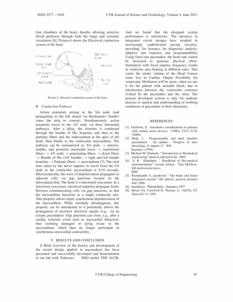
ISSN 2277 – 3916 CVR Journal of Science and Technology, Volume 4, June 2013
CVR College of Engineering 67
four chambers of the heart, thereby allowing selective
blood perfusion through both the lungs and systemic
circulation [6]. Picture-4 shows the Electrical conduction
system of the heart
Picture 4. Electrical conduction system of the heart
B. Conduction Pathway
Action potentials arising in the SA node (and
propagating to the left atrium via Bachmann's bundle)
cause the atria to contract. Simultaneously, action
potentials travel to the AV node via three internodal
pathways. After a delay, the stimulus is conducted
through the bundle of His branches and then to the
purkinje fibers and the endocardium at the apex of the
heart, then finally to the ventricular myocardium. The
pathway can be summarized as: SA node anterior,
middle, and posterior internodal tracts transitional
fibers AV node penetrating fibers distal fibers
Bundle of His (AV bundle) right and left bundle
branches Purkinje fibers myocardium [7]. The total
time taken by the nerve impulse to travel from the SA
node to the ventricular myocardium is 0.19 seconds.
Microscopically, the wave of depolarization propagates to
adjacent cells via gap junctions located on the
intercalated disk. The heart is a functional syncytium. In a
functional syncytium, electrical impulses propagate freely
between communicating cells via gap junctions, so that
the myocardium functions as a single contractile unit.
This property allows rapid, synchronous depolarization of
the myocardium. While normally advantageous, this
property can be detrimental as it potentially allows the
propagation of incorrect electrical signals (e.g., via an
ectopic pacemaker). Gap junctions can close, e.g., after a
cardiac ischemic event such as myocardial infarction,
thus isolating damaged or dying tissue in the
myocardium, which then no longer participate in
synchronous myocardial contractility.
V. RESULTS AND CONCLUSION
A Brief overview of the history and development of
the circuit design applied in pacemakers has been
presented and successfully developed and demonstrated
in our lab with Tektronix DSO model TDS 1012B.
And we found that the designed system
performance is satisfactory. The advances in
integrated circuit designs have resulted in
increasingly sophisticated pacing circuitry,
providing, for instance, for diagnostic analysis,
adaptive rate response and programmability
Using fixed rate pacemaker, the heart rate cannot
be increased to generate physical effort.
Simulation with fixed impulse frequency results
in ventricles area beating at different rates. This
varies the stroke volume of the Heart Causes
some loss in Cardiac Output Possibility for
ventricular fibrillation will be more, when we use
it for the patient with unstable block, due to
interference between the ventricular contracts
evoked by the pacemaker and the Atria. The
present developed system is only for students
practice to analyse and understanding of working
conditions of pacemaker in their laboratory.
REFERENCES
[1] Ouellette, S. Anesthetic considerations in patients
with cardiac assist devices. CNRA, 23(2), 9-20.
(2000).
[2] Roth, J. Programmable and dual chamber
pacemakers: An update. Progress in anes
thesiology, 8, chapter 17. WB
Saunders. (1994).
[3] Michael M. Domach, “ Introduction to Biomedical
engineering” pearson education Inc, 2005.
[4] S. R. Khandpur, “ Handbook of Bio-medical
instrumentation” second edition, Tata McGraw-
hill professional press,
2006.
[5] Ramakantht A. gayakwad “ Op-Amps and linear
Integrated circuits” 4th edition, pearson prentice
hall, 2006.
[6] Anesthesia. Philadelphia: Saunders.1997
[8] Moser SA, Crawford D, Thomas A. AICDs, CC
Nurse;62-73, 1993.

ISSN 2277 – 3916 CVR Journal of Science and Technology, Volume 4, June 2013
68 CVR College of Engineering
MHD Free Convection Effects of Radiating
Memory Flow
Syed Amanullah Hussaini 1
M.V Ramana Murthy 2 and Rafiuddin
3
1M J College of Engineering & Technology, Department of Mathematics, Hyderabad, India
Email: [email protected] 2Osmania University, Department of Mathematics, Hyderabad, India
Email: [email protected]
3CVR College of Engineering, Department of H & S, Ibrahimpatam (M ), R.R.District, A.P., India
Email: [email protected]
Abstract – Two dimensional unsteady radiating oscillatory
memory flow past an infinite plane porous wall is
investigated. Expressions for the mean velocity and the
mean temperature are obtained. The effects of various
parameters such as Permeability parameter (K), Grashoff
number (Gr), Hartmann number (M), Radiation
parameter (N), Prandle number (Pr) are depicted
graphically. Nusselt number (Nu) and Skin friction (Cf)
are discussed by tables.
Index Terms – Suction, Porous medium, Walter’s liquid- B
and Rosseland’s approximation.
I. INTRODUCTION
The study of flow of electrically conducting fluid,
the so-called magneto-hydrodynamics (MHD) has a lot
of attention due to its diverse applications in
astrophysics and geophysics. It is important to study the
effect of the interaction of magnetic field on the
temperature distribution and heat transfer when the
fluid is not only electrically conducting but also when it
is capable of emitting and absorbing thermal radiation.
Heat transfer by thermal radiation is important when we
are concerned with space technology applications and
in power engineering. Seddeek [3] studied the effects of
radiation and variable viscosity on a MHD free
convection flow past an semi-infinite flat plate with an
aligned magnetic field in the case of unsteady flow.
Mazumdar and Deka [4] investigated MHD flow past
an impulsively started infinite vertical plate in presence
of thermal radiation. Analytical closed-form solution of
the unsteady hydro-magnetic natural convection heat
and mass transfer flow of a rotating, incompressible,
viscous Boussinesq fluid was presented by Mbeledogu
and Ogulu [5]. Mbeledogu et al. [6] also studied the
free convection flow of a compressible Boussinesq fluid
under the simultaneous action of buoyancy and
transverse magnetic field. Mohamed and Abo- Dahab
[7] analysis, the effects of chemical reaction and
thermal radiation on hydromagnetic free convection
heat and mass transfer for a micropolar fluid via a
porous medium bounded by a semi-infinite vertical
porous plate in the presence of heat generation. Natural
convection of an electrically conducting and radiating
fluid in the presence of an external magnetic field is
investigated numerically by Young [8]. Zueco and
Anwar [9] studied the steady-state, magneto
hydrodynamic, optically thick, dissipative gas boundary
layer flow and heat transfer past a non-isothermal
porous wedge embedded in a scattering, homogenous,
isotropic Darcy_Forchheimer porous medium, with
significant thermal radiation effects in the presence of
heat sink/sources and surface transpiration, in a (x, y)
coordinate system. Ahmed and Sarmah [10] analyzed
the joint effect of thermal radiation and transverse
magnetic field on an unsteady convection and mass
transfer flow of an incompressible viscous electrically
conducting fluid past a suddenly fixed vertical plate.
Ishak [11] worked mixed convection boundary layer
flow over a horizontal plate with thermal radiation.
Soret and Dufour effects on free convection flow of
non-Newtonian fluids along a vertical plate embedded
in a porous medium with thermal radiation were studied
by Tai and Char [12]. Israel – Cookey and Nwaigwe
[13] considered unsteady MHD flow of a radiating fluid
over a vertical moving heated porous plate with time –
dependent suction. Narahari [14] studied the effects of
thermal radiation and free convection currents on the
unsteady Couette flow between two vertical parallel
plates with constant heat flux at one boundary. Israel –
Cookey et al. [15] investigated the combined effects of
radiative heat transfer and a transverse magnetic field
on steady flow of an electrically conducting optically
thin fluid through a horizontal channel filled with
porous medium and non- uniform temperatures at the
walls. Singh et al. [16] studied the effect of surface
mass transfer on MHD mixed convection flow past a
heated vertical flat permeable surface in the presence of
thermophoresis, radiative heat flux and heat
source/sink. Ahmed [17] given the exact solution to the
problem of MHD transient free convection and mass
ISSN 2277 – 3916 CVR Journal of Science and Technology, Volume 4, June 2013
CVR College of Engineering 69
transfer flow of a viscous, incompressible, and
electrically conducting fluid past a suddenly started
infinite vertical plate taking into account the thermal
diffusion as well as the thermal radiation was presented.
The heat and mass transfer characteristics of the
unsteady electrically conducting fluid flow past a
suddenly started vertical infinite flat plate studied by
Turkyilmazoglu and Pop [18]. Free convective heat and
mass transfer flow over a moving permeable flat
vertical stretching sheet in the presence of non-uniform
magnetic field is numerically investigated by Ferdows
et al. [19].
Now we study the free convection effects on the
fluctuating flow of radiating memory flow past an
infinite porous wall with constant suction through
porous medium.
II. FORMULATION OF PROBLEM
We consider the free convective flow due to
fluctuating mean stream of memory fluid (Walter’s
Liquid Model-B) flow past an infinite plane, porous
wall with constant suction at the surface. Let y=0 be the
wall in the presence of magnetic field normal to the
direction of flow. Let u and v be the velocity
components along and normal to the wall.
We make the following assumptions:
1) That all the fluid properties are constant except the
density in the buoyancy force term;
2) That the term due to the electrically dissipation is
neglected in energy equation (2.2) as the magnetic field
is not strong enough to cause Joule heating (electrical
dissipation)
3) That the Eckert number Ec and the magnetic
Renold’s numbers are small so that the induced
magnetic field can be neglected. The x-axis is taken
along the surface in the upwards direction and y-axis is
taken normal to it.
As the bounding surface is infinite in length, all the
variables are functions of y alone. By the usual
boundary layer approximation the basic equation for
unsteady flow are
where the Rosseland’s approximation
(Brewster[2]) is used, which leads to
The boundary conditions are:
We assumed that the temperature differences within
the flow are sufficiently small such that T4 may be
expressed as a linear function of the temperature. This
was accomplished by expanding T4 in a Taylor series
about T and neglecting higher-order terms. Thus,
Using (2.4) and (2.6) in (2.3) gives
Introducing the following non-dimensional
quantities:
,

ISSN 2277 – 3916 CVR Journal of Science and Technology, Volume 4, June 2013
70 CVR College of Engineering
Using equation (2.2) into (2.3), then with the help of
(2.8), the following equations are obtained
The corresponding boundary conditions becomes
Free-stream boundary condition
Where
Density of fluid,
Kinematic visco-elasticity,
1 Coefficient of volume expansion,
Ho Magnetic intensity,
Magnetic permeability,
Rm Magnetic Renolds number,
Kinematic viscosity,
K Permeability parameter,
Cp Specific heat at constant pressure,
N Thermal radiation parameter,
Thermal conductivity,
Grashoff number,
Prandtl number,
M Hartmann number,
E Eckert number,
q Heat flux,
Electric conductivity,
Stephan-Boltzman constant,
Mean absorption coefficient,
=
III. SOLUTION OF THE PROBLEM
Following Lighthill, [1] we put velocity and
temperature field as
since free stream velocity fluctuates, we may take
Where ‘ is the frequency and is very small
quantity < <1.
Now making use of (3.1) and (3.2) into the equations
(2.9) and (2.10), equating harmonic and non-harmonic
terms, we get
Zeroth order
First order
Boundary conditions are
In equations (3.4) and (3.6), because of the presence
of elasticity term, we get third order differential
equation. To solve this, we need three boundary
conditions but we have two. So following Beard and
Walters (1964), we assume the solution as
Where u0 and 0 are the mean velocity and mean
temperature and u1 and 1 are the fluctuating parts of
the velocity and temperature respectively.
Using equations (3.10) into equations (3.4) – (3.7)
equating the coefficients of different powers of and
neglecting those of
Thereafter considering differential equations related
to mean parts

ISSN 2277 – 3916 CVR Journal of Science and Technology, Volume 4, June 2013
CVR College of Engineering 71
Boundary conditions are
We solve the equations (3.11) – (3.14), we expand
u and in powers of E because of Eckert number E is
very small (< < 1) for incompressible fluid
Replacing F by we get
Boundary conditions are
We get the following solutions for the mean
temperature profiles as
Mean dimensionless coefficient of heat transfer i.e.,
Nusselt’s number is given by
(3.33)
Now we get the following solutions for the mean
velocity profiles.
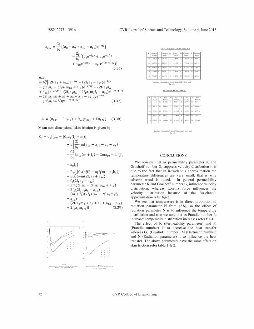
ISSN 2277 – 3916 CVR Journal of Science and Technology, Volume 4, June 2013
72 CVR College of Engineering
(3.36)
Mean non-dimensional skin friction is given by
-100
-80
-60
-40
-20
0
20
40
0 0.5 1 1.5 2 2.5
Pr N
I 1 .1
II .71 .2
III .71 .1
figure-1
Mean temperature distribution 0 versus y for fixed values of
M=5,K=0.1 , Gr=5, E=0.01and Rm=0.4
0
l
ll
lll
y
K* Gr M
l .1 5 10
ll .1 5 5
lll .2 5 5
lV .1 10 5
figure-2
Mean velocity distribution u0versus y for fixed values of
N=0.1,E=0.01 and Rm=0.4
u0
y
lV
lll
ll
l
-60
-50
-40
-30
-20
-10
0
10
0 0.5 1 1.5 2 2.5
K Nusselt’s
Number
Pr Nusselt’s
Number
Gr Nusselt’s
Number
M Nusselt’s
Number
N Nusselt’s
Number
0.2 12136.7 0.2 23105.0 2 19196.8 2 14873.3 0.2 19889.8
0.4 8915.03 0.4 22848.7 4 19210.2 4 17740.4 0.4 20997.3
0.6 7894.28 0.6 20488.8 6 19232.5 6 20729.7 0.6 21844.3
0.8 7394.51 0.8 18269.2 8 19263.8 8 23834.5 0.8 22480.3
1.0 7098.13 1.0 16459.3 10 19304.1 10 27048.8 1.0 22945.5
NUSSELT’S NUMBER TABLE 1
For fixed values of K=0.1,Pr=0.71,Gr=5,M=5, N=0.1and
Rm = 0.4
K Skin
Friction
Pr Skin
Friction
Gr Skin
Friction
M Skin
Friction
N Skin
Friction
0.2 11.182 0.2 26.9039 2 3.6201 2 12.9959 0.2 16.1654
0.4 6.0182 0.4 20.3494 4 9.5948 4 13.9239 0.4 18.5692
0.6 2.7696 0.6 17.5894 6 20.2742 6 14.3923 0.6 19.7510
0.8 0.6292 0.8 10.6247 8 38.0083 8 14.6059 0.8 20.2481
1.0 -0.8731 1.0 0.41004 10 65.1472 10 14.6717 1.0 20.3468
SKIN FRICTION TABLE 2
For fixed values of K=0.1,Pr=0.71,Gr=5,M=5, N=0.1and
Rm = 0.4
CONCLUSIONS
We observe that as permeability parameter K and
Groshoff number Gr suppress velocity distribution it is
due to the fact that in Rosseland’s approximation the
temperature differences are very small, that is why
adverse trend is noted. In general permeability
parameter K and Groshoff number Gr influence velocity
distribution, whereas Lorentz force influences the
velocity distribution because of the Roseland’s
approximation refer fig-2
We see that temperature is in direct proportion to
radiation parameter N from (2.8), so the effect of
radiation parameter N is to influence the temperature
distribution and also we note that as Prandle number Pr
increases temperature distribution increases refer fig-1
The effect of K (Permeability parameter) and Pr
(Prandle number) is to decrease the heat transfer
whereas Gr (Grashoff number), M (Hartmann number)
and N (Radiation parameter) is to influence the heat
transfer. The above parameters have the same effect on
skin friction refer table 1 & 2.

ISSN 2277 – 3916 CVR Journal of Science and Technology, Volume 4, June 2013
CVR College of Engineering 73
REFERENCES
[1] M.J. Lighthill “The response of laminar skin friction and
heat transfer to fluctuation in the stream velocity”
Proceedings of the Royal Society, A 224,1. (1954)
[2] M.Q. Brewester, “Thermal radiative transfer and
properties” New York, John Wiley and Sons Inc. (1992)
[3] M.A. Seddeek, “Effects of radiation and variable viscosity
on a MHD free convection flow past a semi-infinite flat
plate with an aligned magnetic field in the case of
unsteady flow” International Journal of Heat and Mass
transfer 45 (2002) 931-935
[4] M.K. Mazumdar and R.K. Deka, “MHD flow past an
impulsively started infinite vertical plate in presence of
thermal radiation”, Romanian Journal of Physics, 52(5-
7), (2007) 565-573
[5] I.U. Mbeledogu and A. Ogulu, “Heat and mass transfer of
an unsteady MHD natural convection flow of a rotating
fluid past a vertical porous flat plate in the presence of
radiative heat transfer” International Journal of Heat and
Mass Transfer 50 (2007) 1902–1908
[6] I.U. Mbeledogu, A.R.C. Amakiri and A. Ogulu,
“Unsteady MHD free convective flow of a compressible
fluid past a moving vertical plate in the presence of
radiative heat transfer” International Journal of Heat and
Mass Transfer 50 (2007) 1668–1674
[7] R.A. Mohamed and S.M. Abo-Dahab, “Influence of
chemical reaction and thermal radiation on the heat and
mass transfer in MHD micro polar flow over a vertical
moving porous plate in a porous medium with heat
generation” International Journal of Thermal Sciences 48
(2009) 1800–1813
[8] C. Y. Han, “Hydromagnetic free convection of a radiating
fluid” International Journal of Heat and Mass Transfer
52 (2009) 5895–5908
[9] J. Zueco and O. A. Beg “Network simulation solutions for
laminar radiating dissipative magneto-gas dynamic heat
transfer over a wedge in non-Darcian porous regime”
Mathematical and Computer Modelling 50 (2009) 439 -
452
[10] N. Ahmed and H.K. Sarmah, “Thermal radiation effect
on a transient MHD flow with mass transfer past an
impulsively fixed infinite vertical plate”, International
Journal of Applied Mathematics and Mechanics 5
(2009) 8798.
[11] A. Ishak, “Mixed convection boundary layer flow over a
horizontal plate with thermal radiation” Heat Mass
Transfer 46 (2009) 147–151.
[12] Bo-C. Tai and M.-I. Char, “Soret and Dufour effects on
free convection flow of non- Newtonian fluids along a
vertical plate embedded in a porous medium with
thermal radiation” International Communications in Heat
Mass Transfer 37 (2010) 480–483.
[13] C.I.Cookey and C. Nwaigwe, “Unsteady MHD flow of a
radiating fluid over a moving heated porous plate with
time – dependent suction”, American Journal of
Scientific and Industrial Research, (2010) 1(1): 88 –
95.
[14] M. Narahari, “Effects of thermal radiation and free
convection currents on the unsteady Couette flow
between two vertical parallel plates with constant heat
flux at one boundary”, World Scientific and Engineering
Academy and Society Transactions on Heat and Mass
Transfer, (2010) 1(5): 21 – 30.
[15] C.I Cookey, V. B. O. Pepple and I. Tamunobereton-ari
“On steady hydromagnetic flow of a radiating viscous
fluid through a horizontal channel in a porous medium”
American Journal of Scientific and Industrial Research,
(2010), 1(2): 303-308
[16] N.P. Singh, A.K. Singh, A.K. Singh and P. Agnihotri,
“Effects of thermophoresis on hydromagnetic mixed
convection and mass transfer flow past a vertical
permeable plate with variable suction and thermal
radiation” Communications in Nonlinear Science and
Numerical Simulation 16 (2011) 2519–2534
[17] N. Ahmed, “Soret and radiation effects on transient
MHD free convection from an impulsively started
infinite vertical plate” J. Heat Transfer 134 (2012)
062701-1–062701-9.
[18] M. Turkyilmazoglu and I. Pop, “Soret and heat source
effects on the unsteady radiative MHD free convection
flow from an impulsively started infinite vertical plate”
International Journal of Heat and Mass Transfer 55
(2012) 7635–7644
[19] M. Ferdows, M.J. Uddin and A.A. Afify, ”Scaling
group transformation for MHD boundary layer free
convective heat and mass transfer flow past a
convectively heated nonlinear radiating stretching sheet”
International Journal of Heat and Mass Transfer 56
(2013) 181–187

ISSN 2277 – 3916 CVR Journal of Science and Technology, Volume 4, June 2013
74 CVR College of Engineering
A Brief Overview of Some Environmental
Problems in India K.T. Padmapriya
1 and Dr. Vivekanada Kandarpa
2
1 CVR College of Engineering, Department of H&S, Ibrahimpatan, R.R.District, A.P., India
Email:[email protected] 2 Professor, University of Phoenix, USA.
Email: [email protected]
Abstract- The current article is a brief discussion of the
enormity of environmental problems facing India. The
problems are in the form of pollution of air, water, and land
resources. High concentrations of pollutants of various
kinds are directly linked with the health of the people, and
in some cases they result in premature deaths. It is extreme-
ly important for engineers of the current and next genera-
tion to be cognizant of this situation in their future devel-
opments. Environmental laws exist, and every effort should
be made to keep this in mind in all new developments.
Index Terms- Environment, Atmospheric pollution,
pollutant, Environmental laws.
I. INTRODUCTION
There is a preponderance of evidence that the majori-
ty of the respiratory and cardiovascular maladies, cancer
and other serious diseases, and even premature death of
millions of infants are due to very high level of the pollu-
tion of the air, water, and land. The sources for the pollu-
tion are many, and they include various industries, elec-
tric power plants, different modes of transportation, and
waste disposal of various kinds (medical, industrial, ra-
dioactive, etc.,). In spite of the promulgation of many
government regulations to combat the degradation of the
environment, very little progress is being made and even
the little progress made to date is too slow, especially in
the developing countries. This is in spite of the global
alarm expressed in the United Nations sponsored GEO-4
[1]: “Tipping points occur when the cumulative effects of
steady environmental changes reach the thresholds that
result in dramatic and often rapid changes. There is a
concern that a number of environmental systems may be
heading towards tipping points.”
Most of the well developed countries are making
much better progress at the local level in reducing harm-
ful pollution, but many of them are reluctant to take full
measures to reduce green house gas (GHG) emissions.
Their main reasons expressed by the developed countries
for the resistance to fully implement any reduction in
GHG emissions are: (1) economic impact of such meas-
ures on the industry and (2) the lack of general belief on
the GHG impact on global warming. On the other hand,
the developing countries are reluctant to do anything re-
garding GHG emissions for a different set of reasons.
They include: (1) the current urgent need of energy and
other resource needs to support large populations, (2) a
general lack of clean energy resources, and (3) the eco-
nomic impact of importing advanced technologies to im-
plement these reductions.
The purpose of this article is to educate the current gen-
eration of Engineers on the seriousness of the environ-
mental problems currently facing India.
II. BRIEF HISTORICAL BACKGROUND
Historically speaking, the general concerns for the
environment were expressed in Indian literature as far
back as 300 BC in Kautilya’s Arthasastra, where econom-
ic importance of forest administration is emphasized [2].
Following the ideas expressed in this document, Ashoka,
in the early part of 1st Century implemented some con-
crete measures, as evident on the Ashoka Pillar, which
expresses the necessity for biodiversity [3]:
"- - - - - Beloved-of-the-Gods, King PIYADASI
(ASHOKA), speaks thus: Animals were declared to be
protected – parrots, bats, - - - - and all four-footed crea-
tures that are neither useful nor edible. Also protected
were nanny goats, ewes and sows which are with young
or giving milk to their young, and so are young ones less
than six months old. Cocks are not to be caponized, husks
hiding living beings are not to be burnt, and forests are
not to be burnt either without reason or to kill creatures."
Additional evidence for the Indian society concern
for environment can be found in the 5th
Century docu-
ment named “YAGNAVALKYA SMRITHI”, which
prohibited the cutting of trees and prescribed punishment
for such acts.
These historical documents clearly demonstrated that
the Indian society was implicitly conscious of the adverse
environmental effects caused by deforestation and extinc-
tion of animal species (i.e. harmful effects of bio diversi-
ty). The latest GEO-4 [1] stresses the importance of bio-
diversity in preserving human and ecosystem welfare.
However, over a period of several centuries, India lost
this ideology and substantially deviated from its historic
ethical philosophy and started embracing western utilita-
rian ethical philosophy. From the advent of industrial
revolution, the utilitarian western ethical philosophy es-
sentially dictated indiscriminate use of natural resources,

ISSN 2277 – 3916 CVR Journal of Science and Technology, Volume 4, June 2013
CVR College of Engineering 75
in the beginning in the western countries, and subsequent-
ly propagated throughout the world. According to utilita-
rian ethics, the right action is “the action that produces
maximum happiness to man”. It is generally accepted
that “the main strands of Judeo-Christian thinking had
encouraged the overexploitation of nature by maintaining
the superiority of humans over all other forms of life on
earth, and by depicting that all of nature as created for the
use of humans”[4][5]. However, in the mid to late 20th
century, many U.S. naturalists began to rethink some of
these ethical viewpoints and started to voice concerns on
the overuse of natural resources. They promoted the idea
of conserving natural resources and eventually forced the
legislative actions of the U.S. administration. The public
awareness about the pollution and the degradation of the
resource quality began to increase, in large part because
of the publication of the book, Silent Spring by Rachel
Carson [6]. Her book emphasized the harmful effects of
DDT (dichlorodiphenyltrichloroethane) and other pesti-
cides on birds as well as the contamination of human
food supplies. Subsequently, further environmental
movements followed throughout the U.S. and finally by
1970, the voices of the environmentalists were heard with
the establishment of the first Earth Day by Gaylord Nel-
son, a former U.S. senator. Soon after, the US govern-
ment formed Environmental Protection Agency (EPA)
and established National Environmental Policy Act (NE-
PA). Now, most of the countries around the world have
incorporated some form of environmental legislation to
protect the environment. The EPA passed many environ-
mental laws and regulations aimed at protecting the envi-
ronment. However, it is not an easy task to implement the
laws, especially when it comes to retrofitting changes to
the already well established industries in the U.S. In spite
of these difficulties, U.S. and many of the developed
countries have been making substantial progress.
The developing countries, such as India, China, and
other countries are facing similar environmental prob-
lems, but with more enhanced intensities due to relatively
large populations using technologies. Before the prob-
lems get too severe, these developing countries should
pay attention to the “lessons already learned” by the de-
veloped countries and implement the proper preventive
measures at the inception of any new industrial develop-
ments. One of the crucial steps in this process is a general
awareness of how natural environment functions.
III. WHAT IS ENVIRONMENTAL SCIENCE?
Environmental Science is the application of different
sciences and non-sciences in understanding and manag-
ing or mismanaging the environment around us. It is not
like other pure sciences. The goal of pure sciences is “to
find how world works, to seek what regularities there
may be, to penetrate to the connection of things – from
sub-nuclear particles, which may be the constituents of all
matter, to living organisms, the human social community,
and thence to the cosmos as a whole” [7]. Science, espe-
cially physics attempts to understand the functioning of
the universe, simply because it is there. In spite of the
esoteric nature of sciences and its focus on fundamental
research, humans benefited from the technologies they
produced. However, some of the technological develop-
ments resulted in several unexpected consequences, such
as “damages of various kinds” to the environment around
us. There are many historical examples related to the
“unexpected negative consequences” of useful technolo-
gical products. Let us look at a recent example of a wide-
ly used pesticide which is banned subsequently because
of the unexpected consequences.
NEONICOTINOID pesticides, a group of nicotine
based chemicals, have been successfully helping in the
control of pests of various kinds. Different research or-
ganizations, including the most recent work, hailed these
pesticides to “have outstanding potency and systemic
action for crop protection against piercing-sucking pests,
and they are highly effective for flea control on cats and
dogs. They generally have low toxicity to mammals
(acute and chronic), birds, and fish.”[8]. Since their regis-
tration in 1990’s, these pesticides have been in use
throughout the world. In recent research activities, a poss-
ible link between the use of NEONICOTINOID pesti-
cides and drastic reduction in honey bees has been estab-
lished. As the honey bees are considered the prime polli-
nators in agriculture, a majority of the countries in the
European Union banned the use of NEONICTONOID
pesticides. It is definite win for the bees and the environ-
mentalists [9]. Further studies, probably, will ban the use
of these pesticides in other countries. This example illu-
strates the relation among sciences, technologies, envi-
ronmentalists, and government. Thus environmental
science, unlike pure sciences is driven by humans for
their need. Environmental Scientists are like “watch-
dogs” for the people and government agencies in propos-
ing and implementing various environmental laws.
By its complex nature, environmental science han-
dles many interconnected local as well as global issues
involving human population, natural resources, and envi-
ronmental pollution. It recognizes that whatever we do,
that is going to alter the world’s environment outside
humans. The goal of environmental science is to encour-
age various governments, industries and people of the
world to operate in an environmentally sustainable man-
ner. Here, the environmental sustainability is defined as
the ability to meet the current human needs for natural
resources without compromising the ability of future gen-
erations to meet their needs, including minimum to the
environment.
IV. ENVIRONMENT AS A SYSTEM: Natural Envi-
ronment
As in Science and Engineering disciplines, it is con-
venient and useful to treat the environment as a system.
The environmental system may be considered as made up
four segments or individual sub-systems: Atmosphere,
Hydrosphere, Geo-sphere or Lithosphere, and Biosphere.
Fig.1 illustrates a schematic of natural environmental
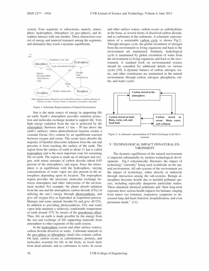
ISSN 2277 – 3916 CVR Journal of Science and Technology, Volume 4, June 2013
76 CVR College of Engineering
system. Four segments or subsystems, namely, atmos-
phere, hydrosphere, lithosphere (or geo-sphere), and bi-
osphere interact with one another. These interactions con-
sist of energy and material transport among the segments,
and ultimately they reach a dynamic equilibrium.
Figure 1: Schematic Representation of Natural Environment
Sun is the main source of energy in supporting life
on earth. Earth’s atmosphere provides radiation protec-
tion and molecular exchange needed to support life. Very
high energy radiation from the sun is protected by the
stratosphere (between about 11 km – 50 km above the
earth’s surface), where photochemical reaction creates a
constant Ozone (O3) content by an equilibrium reaction
between oxygen and ozone. The ozone layer absorbs the
majority of harmful ultraviolet radiation from the sun and
prevents it from reaching the surface of the earth. The
region from the surface of earth to about 11 km is called
troposphere and is the most important zone for sustaining
life on earth. The region is made up of nitrogen and oxy-
gen, with minor amounts of carbon dioxide (about 0.03
percent of the atmosphere), and argon. Since the atmos-
phere is in equilibrium with the hydrosphere, varying
concentrations of water vapor are also present in the at-
mosphere depending upon its location. The troposphere
region provides the necessary molecular exchange be-
tween atmosphere and other subsystems of the environ-
ment needed. For example, the plants absorb radiation
from the sun and the atmospheric carbon dioxide (CO2) in
utilizing the sun’s energy through photosynthesis, and
give off oxygen (O2) as byproduct in respiration process.
Humans and some animals breathe O2 and give off CO2.
In addition to providing photosynthesis, CO2 and water
vapor help maintain a relatively comfortable temperature
of earth around 15oC by means of the greenhouse effect.
Thus, life on earth is made possible by the energy from
the sun and exchange of life supporting materials from
atmosphere to other segments of the earth system.
In the hydrosphere (ocean and other surface waters),
carbon dioxide dissolves in water. Carbonate minerals in
the geo-sphere or lithosphere (land) also contain carbon.
On land, carbon occurs as carbohydrates, proteins, and
molecules essential for life in the biota, as fossil fuels
from dead animals, and as carbonates in rocks. In ocean
and other surface waters, carbon occurs as carbohydrates
in the biota, as several forms of dissolved carbon dioxide,
and as carbonates in the sediments. A schematic represen-
tation of a sustainable carbon cycle is shown Fig.2,.
Through nitrogen cycle, the global circulation of nitrogen
from the environment to living organisms and back to the
environment are maintained. Similarly, hydrological
cycle is maintained by global circulation of water from
the environment to living organisms and back to the envi-
ronment. A standard book on environmental science
should be consulted for additional details on various
cycles [10]. A dynamic balance of carbon, nitrogen, wa-
ter, and other constituents are maintained in the natural
environment, through carbon, nitrogen, phosphorus, sul-
fur, and water cycles.
Figure 2: A schematic representation of Carbon Exchange in the Envi-
ronment
V. TECHNOLOGICAL IMPACT ONNATURAL EN-
VIRONMENT
The dynamic equilibrium of the natural environment
is impacted substantially by modern technological devel-
opments. Fig.3 schematically illustrates the impact of
technology “currently” being used worldwide on the nat-
ural environment. All sub-systems of the environment see
the impact of technology, either directly or indirectly
through interaction among the sub-systems. Benign at-
mosphere becomes hostile due to harmful pollutant spe-
cies, including especially dangerous particulate matter.
These unnatural chemical pollutants and “their long-term
exposure have serious health impacts for humans, ranging
from minor eye irritation, respiratory symptoms to de-
creased lung and heart function, hospitalization, and even
premature death.” [11].
Carbon stored in the
atmosphere
Carbon stored on land:
Biota, rocks, soil, and
fossil fuels
Carbon stored in
ocean: Biota, water,
and sediment

ISSN 2277 – 3916 CVR Journal of Science and Technology, Volume 4, June 2013
CVR College of Engineering 77
Figure 3: IMPACT OF TECHNOLOGY ON THE NATURAL
ENVIRONMENT
The introduction of technology imparts additional
constituents in all subsystems of the natural environment.
Some of the technologies which directly impacted the
natural environment include,
1) Energy production and utilization industries
(fossil fuels including coal)
2) Transportation industries and private transporta-
tion (fossil fuels use)
3) Agriculture practices
4) Manufacture and utilization pesticides and insec-
ticides
5) Manufacture of industrial products and various
chemicals (Most of the Chlorine based chemi-
cals)
6) Extraction and processing of mineral extraction
(various acids, surfactants, etc.,)
7) Waste disposal (medical, radioactive, etc.)
These and many more modern developments contri-
bute to the degradation of the environment. For example,
coal mining industry and the burning of coal in the power
generation industry cause serious environmental prob-
lems. Mining destroys existing vegetation and topsoil; the
effluents in the mining operation generate pollutants in
water and in the air (arsenic, lead, cadmium, particulate
matter, etc.). Combustion of carbon produces several pol-
lutants (CO2, SO2, etc). The GEO-4 of the UNEP empha-
sized that the energy, climate-change, industrial devel-
opments and environmental pollution are the main envi-
ronmental concerns [1]. The report further reiterated that
twenty years after the first report (UNEPT, 1998), factors
such as population growth, and economic activities as
well as consumption patterns have placed increased pres-
sure on the environment. The population growth and in-
crease in economic activities affect the environment ne-
gatively. The result is greater consumption of resources
and higher pollution. However, by implementing im-
provement in technology, the negative effects of technol-
ogy can be minimized or even eliminated.
VI. ATMOSPHERIC POLLUTION
The atmosphere, its pollutants and their associated
issues are very complex. Here atmospheric pollution is
defined as chemicals added to the “natural environment”
in high enough concentrations to be harmful. The addi-
tion of these chemicals could occur by natural events
(volcanic activity) or human activities (emissions from
transportation and various industries). A given pollutant
can have local or global effect depending upon the resi-
dence time of the pollutant in the atmosphere. The resi-
dence time of a pollutant is a measure of how long it
stays in the atmosphere. The pollutants with short resi-
dence times affect local air quality. The pollutants that
affect local air quality include particular matter (PM),
gases such as SO2, NO2, NO, NH3 and their ionic forms.
All the gaseous species mentioned are called primary
pollutants (emitted directly into atmosphere). The pollu-
tants with residence time of days to weeks cause local
and regional problems. The pollutants that belong to this
category include, SO4-2
, NO3 -, NH4
+, and particular mat-
ter having PM2.5 (particulate matter with diameters less
than or equal to 2.5 microns). The pollutants with resi-
dence time of weeks to months cause continental prob-
lems. The presence of Ozone in the troposphere belongs
to this category. Ozone in the troposphere is formed as a
result of secondary conversion of nitrogen oxides and
some hydrocarbons in the presence of UV radiation. The
pollutants with residence time from month to years result
in global problems, including global warming. Pollutants
that belong to this category are CO2, CH4, N2, SF6, HFCs,
and PFCs.
The immediate effect of air pollution is its impact on
human health. Evidence shows that many air pollutants
suppress the immune system, cause respiratory illnesses,
chronic respiratory diseases and premature death. The
World Health Organization (WHO) uses six atmospheric
pollutants in evaluating air quality. These include, Sus-
pended Particular matter (SPM), Sulfur dioxide, Carbon
monoxide, Ozone (troposphere), and lead. The particulate
pollution in the atmosphere alone seems to be the leading
cause of premature deaths in India and other Asian coun-
tries. In year 2000, over 500,000 premature deaths were
reported as due to outdoor exposure to PM10 particulate
materials. TABLE 1 lists the health effects of the WHO
pollutants. If remedial effects are not implemented, the
premature deaths could reach millions in future.
In addition to the atmospheric pollution, the land and
water resources are also being degraded by various indus-
tries and people by improper discharge of harmful chemi-
cals with consequences to the human and ecosystem
health.

ISSN 2277 – 3916 CVR Journal of Science and Technology, Volume 4, June 2013
78 CVR College of Engineering
TABLE 1
HEALTH EFFECTS AND ATMOSPHERIC POLLUTION
POLLUTANT SOURCE HEALTH EF-
FECTS
Particulate Motor vehicles,
power plants,
various industries,
and construction
Respiratory ill-
nesses, heart
disease, sup-
presses immune
system, some
specific species
may cause cancer.
Nitrogen
Oxides
Motor vehicles,
various industries,
and fertilizer usage
Respiratory con-
ditions
Sulfur Dioxide Power plants and
various industries
Same effects as
particulate matter
Carbon Monox-
ide
Motor vehicles
and various indus-
tries
Headache, fatigue
and death when
exposed to high
level
Ozone Secondary pollu-
tion in the tropos-
phere
Aggravates respi-
ratory conditions,
irritation of eyes
Carbon dioxide Fossil fuel use in
power plants and
various industries,
transportation, and
deforestation
Global warming
and associated ill
effects.
VII. ENVIRONMENTAL ISSUES IN INDIA
For the past fifty years, India has seen tremendous
industrial and technological progress. This rapid growth
is accompanied by innumerable environmental conse-
quences. There is clear visible evidence of the pollution
in many parts of India. A recent article in Slate Magazine
reported that the air pollution in New Delhi is worse than
the air pollution in Beijing, which itself made headlines
around the world for its appalling air quality (Upton,
2013). The constituents of the pollution include particular
matter, nitrogen oxides (NOx), Carbon dioxide (CO2),
Ozone molecules, and many other hazardous chemicals.
This is substantiated by a recent article on Delhi’s parti-
culate (PM) pollution in the Environmental Development
magazine [11]. Other Indian cities have similar air pollu-
tion problems. Another news item reports pollution by
high concentration of PM2.5 [12]. The main sources of the
pollutants are the vehicle exhaust, industries, waste burn-
ing, and construction. The paper reported that between
2008 and 2011, the particular pollution averaged
for PM2.5 and ,
both exceeding the national standards of
and , respectively. Here, the PM2.5 refers to the
particular matter with diameters less than or equal to 2.5
microns and refers to concentration in micro-
grams per cubic meter. Worldwide studies have consis-
tently demonstrated that exposure to PM, NOx, and
Ozone pollution cause serious damage to respiratory and
cardiovascular diseases, in some cases resulted in prema-
ture deaths [13] [14] [15] [16] [17].
A similar state of affairs exists in the case of water
pollution. A recent study on the status of water quality in
Delhi concluded that its surface water is highly polluted
and groundwater is not fit for domestic and drinking pur-
pose [18]. Other major cities in India face similar pollu-
tion problems, as evidenced by a brief stay in any of the
larger cities. Besides air pollution and water pollution,
India faces other major environmental issues on solid
waste pollution, noise pollution, and land or soil pollu-
tion.
In 1997, the United National Environment program
(UNEP) report published a report on global environmen-
tal outlook [19]. The report recognizes that Environmen-
tal problems are extremely complex as a result of interac-
tion among the various components of the environment.
For example, the emissions of greenhouse gases (CO2,
CH4, etc.) and acidifying gases (SO2, NO2) have been
shown to worsen the problem of ozone layer thinning.
VIII. GLOBAL ENVIRONMENTAL ISSUES
Various environmental problems exist in every cor-
ner of the world and most of them are attributed to the
continuing progress or technological developments in
different countries. Just from the point view of air pollu-
tion, based on the air monitoring data between 2003 and
2010, the world’s worst pollution floats over Ahwaz, Iran
followed by Ulaanbaatar, Mongolia [20]. Besides air pol-
lution, other forms of environmental degradation exist
throughout the world. According to a 1998 report by
Canadian Scientists, the entire world is now polluted and
even the most remote Polar Regions have substantial le-
vels of toxic waste presence [21].
It is generally recognized that the environmental
problems are extremely complex as a result of interaction
among the various components of the environment. For
example, the emissions of greenhouse gases (CO2, CH4,
etc.) and acidifying gases (SO2, NO2) have been shown to
worsen the problem of ozone layer thinning. However,
the report issued specific recommendations for India (see
Table 2). All these issues are associated with human
health and natural ecological risks. To mitigate the prob-
lems listed in Table 1, a general understanding of some
aspects of Environment Science is essential.

ISSN 2277 – 3916 CVR Journal of Science and Technology, Volume 4, June 2013
CVR College of Engineering 79
TABLE 2
RESOURCE AND ENVIRONMENTAL ISSUES
HIGH PRIORITY MEDIUM PRIOR-
ITY
LOW PRIORITY
Land and Soil Re-
source
Pesticide and Ferti-
lizer
Sea Level Rise
Deforestation Acid Rain Waste Disposal
Water Resources Marine and Costal
Degradation
Industrial Pollution
Urban Congestion
and Pollution
IX. CONCLUSION
The present article briefly describes the impact of
technology on the natural environment. The impact is in
the form of (1) pollution of the atmospheric air with toxic
chemicals and particulate matter, (2) pollution of water
resources with toxic chemicals, affluent disposals from
industries, and sediments, and (3) pollution of land by
waste disposals and spills. In the earth system, all the
subsystems are interconnected and interact with one
another, and as a result the pollution in one system goes
to contaminate other systems. The effect of pollution of
all systems contributes to millions of cases of pulmonary
and other diseases. In many cases, they result in prema-
ture death, especially of infants.
The sources of pollutants are transportation, chemical,
and power plant industries. It is extremely important to
minimize the pollution through technological innovation
of all industries. All nations have environmental regula-
tions, and new generation of engineers should implement
methods to follow these regulations in all future designs.
REFERENCES
[1]. UNEP, GEO -4, 2007. Global Environmental Out-
look. http://www.unep.org/geo/geo4/report/GEO-4
[2]. Gosh Ray, R., 1996. The attitude of Kautilya to
Aranya. Environment and History 2, no. 2, 221-229,
http://www.environmentandsociety.org/node/2885.
[3]. Buddhist Publication Society, 1994. The Edicts of
King ASHOKA.
[4]. White, 1967. White, L., 1967. “The Historical Roots
of Our Ecological Crisis”, Science, 155:1203-1207.
[5]. Bible, 2001.Genesis1:26.
http://biblehub.com/genesis/1-26.htm
[6]. Rachel Carson, Author- Silent Spring, published by
Houghton Mifflin on September 27, 1962.
[7]. Sagan, C. Broca’s Brain. , Random House, Inc. See
Ch.1 Can we know the Universe? Reflections on a
Grain of Salt.
[8]. Motohiro Tomizawa and John E. Casida, Annual
Review of Pharmacology and Toxicology, Vol. 45:
247-268 (Volume publication date February 2005).
[9]. Victory for the Bees, 2013.
http://www.independent.co.uk/environment/nature/vic
tory-for-bees-as-european-union-bans-neonicotinoid-
pesticides-blamed-for-destroying-bee-population-
8595408.html
[10]. Ahluwalia, V.K. and Malhotra, S., 2008. Environmen-
tal Science. Ane Books India, New Delhi, India.
[11]. Guttikunda, S.K. and Goel, R, 2013. Health impacts
of particulate pollution in a megacity – Delhi, India,
Environmental Development, Environmental Devel-
opment, Volume 6, April 2013, Pages 8–20 Also see:
http://dx.doi.org/10.1016/j.envdev.2012.12.002
[12]. Mascarenhas, A. Pune Air is more polluted now: New
data shows.
http://www.indianexpress.com/news/pune-air-more-
polluted-now-new-data-shows/1082087/
[13]. Chhabra, S.K., Chhapra, P, Rajpal, S., Gupta, R.,
2001. K. Ambient air pollution and chronic respirato-
ry morbidity in Delhi. Archives of Environmental
Health 56, 8.
[14]. Pande, J.N., Bhatta, N., Biswas, D., Pandey, R.M. Ah-
luwalia, G., Siddaramiah, N.H., et al., 2002. Outdoor
air pollution and emergency room visits at a hospital
in Delhi. The Indian Journal of Chest Diseases and
Allied Sciences 44, 9.
[15]. Gupta, S.K., Gupta, S.C., Agarwal, R., Sushma, S.,
Agrawal, S.S., Saxena, R., 2007. A multicentric case-
control study on the impact of air pollution on eyes in
a metropolitan city of India. Indian Journal of Occu-
pational Environmental Medicine 11, 37-40.
[16]. Siddique, S., Banerjee, M., Ray, M., Lahiri, T., 2010.
Air pollution and its impact on lung function of child-
ren in Delhi, the capital city of India. Water, Air, and
Soil Pollution 212, 89-100.
[17]. Balakrishnan, K., Ganguli, B., Ghosh, S., Samban-
dam, S., Roy, S., Chatterjee, A., 2011. A spatially dis-
aggregated time-series analysis of the short-term ef-
fects of particular matter exposure on mortality in
Chennai, India. Air Quality, Atmosphere and Health,
1-11Jones, J. “Entire World Polluted, Canadian Scien-
tist Report.” October 12, 1998, Reuters News Agency.
[18]. Abhay, R.K. Status of water quality and pollution as-
pect in Delhi. International Journal of Social Science
Tomorrow, vol. 1, no. 5. Also see
http://www.ijsst.com.
[19]. UNEP, GEO-1., 1997. Global Environmental Out-
look. http://www.unep.org/geo/geo1
[20]. Upton, J., 2013. Slate Magazine article: Which City
has the Worst Air Pollution in the World?
http://www.slate.com/articles/health_and_science/me
dcal_examiner/2013/03/worst_air_pollution_in_the_
world_beijing_delhi_ahwaz_and_ulaanbaatar.html
[21]. Jones, J. “Entire World Polluted, Canadian Scientist
Report.” October 12, 1998, Reuters News Agency.

ISSN 2277 – 3916 CVR Journal of Science and Technology, Volume 4, June 2013
80 CVR College of Engineering
Software Quality Estimation through Analytic
Hierarchy Process Approach
B. B. Jayasingh, Professor, IT Dept., CVR College of Engineering, Ibrahimpatan, RR Dist-501510.
Email: [email protected]
B. Rama Mohan !Associate Professor, CSE Dept., JNTUH College of Engineering, Hyderabad – 500085, (AP).
Email: [email protected]
Abstract--Software quality assurance plays an important
role to justify the software to reach the right level of
quality. Its objective is to estimate the software quality
and the errors in software modules before release to
market place. In order to estimate the right level of
quality one must apply some comprehensive techniques.
To determine software quality, we present the Analytic
Hierarchy Process (AHP) is the suitable approach for
assessing the quality of software, with judgments by a
group of experts rating. Since developing perfect or highly
compatible software is not easy the AHP approach puts a
threshold beyond which the quality of the new
development is more than acceptable. We studied various
techniques approached by different authors of software
quality assurance to enable the stakeholder for choosing
right kind of techniques suitable to their project.
Index Terms—Analytic Hierarchy Process, In Vivo
Testing, Source Code Metrics, Software Quality, Divide
And Conquer, Prioritization Problem.
I. INTRODUCTION
Software runs on the machine and machine finds the
errors with human interaction while development
process. The development phase of SDLC (Software
Development Life Cycle) includes more formal and
detailed technical reviews that ensure to detect errors
early. It is the time now for face-to-face communication
instead of formal reviews, so the teams to decide and
own the quality of each product. The product quality
will be higher through the agile [1] development
process that many organizations belief.
One specific form of technical debt [2] that has been
studied for some time is design debt, also referred to as
architecture debt. Design debt occurs whenever the
software design no longer fits its intended purpose. A
software project can run into design debt for various
reasons. For example, adding a series of features that
the initial architecture was not intended to support can
cause debt and decrease the maintainability of software.
Or, drifting away from a proposed architecture can
bring short-term payoffs but might have consequences
for the portability and interoperability of software.
Reducing or eliminating design debt means in most
cases that the design should be tailored and adapted
towards changing requirements immediately and
continuously.
We study various techniques approached by different
authors of software quality assurance to enable the
stakeholder for choosing right kind of techniques
suitable to their project. The most important goals of
the software industry is to develop high-quality and
reliable software for their customers. We also consider
the in vivo testing, in which tests are continuously
executed in the deployment environment. However, the
technical quality of source code (how well written it is)
is an important determinant for software
maintainability. Our survey focuses the low level
source code metrics also effect to the high level quality
characteristics. One must reconsider the divide and
conquer principle applied consistently throughout the
development (requirements documentation, design,
review, coding, inspection, and testing) and
maintenance of the product. However, predicting the
exact number of faults is too risky, especially in the
beginning of a software project when too little
information is available. We conclude the analytical
hierarchy process is the best suitable approach for
software quality assurance.
In section II we discuss about the in vivo testing that
run in the deployment environment which is hidden to
the user. In section III we discuss the technical quality
of source code (how well written it is) and how it
affects to software maintainability. In section III we
discuss the source code metrics that affect to the high
level quality characteristics. In section IV we discuss
the mathematical model for software quality assurance
called divide and conquer where the complex job of
building a software product must be reduced to a set of
much simpler jobs. In section V we discuss the analytic
hierarchy process consists of 6 criteria and 27
subcriteria where the prioritization problem solved to
estimate the quality of software.

ISSN 2277 – 3916 CVR Journal of Science and Technology, Volume 4, June 2013
CVR College of Engineering 81
II. IN VIVO TESTING APPROACH
Testing at deployment environment needs attention
of the developer where it runs continuously without the
knowledge of user [3]. It is an improved version of unit
or integration tests and focusing on aspects of the
program that should hold true regardless of the state of
the system. These tests keep the current state of the
program while execution without affecting or altering
the state that visible to users. This testing can be used to
detect concurrency, security, or robustness issues.
In vivo testing [3] is a methodology by which tests
are executed continuously without disturbing the state
of the system that is hidden to the user. A prototype is
developed in JAVA programming language called
Invite (IN VIvo TEsting framework), focused on
distributed execution of tests in earlier version. The
current version includes a more detailed description in
which it reveals the defects in real world applications.
A. In Vivo Testing Framework
The in vivo testing framework describes the steps
for a software vendor regarding to use the Invite
framework. The development of any new test code and
the configuration of the framework must be done prior
to distribute an in vivo-testable system.
1. Create test code
The test methods must reside in the same class
as the code they are testing (or in a superclass).
2. Instrument classes
The vendor must select the methods from one
or more Java classes in the application that
under test for instrumentation.
3. Configure frameworks
Each method runs with probability ρ, the
vendor must configure Invite with values
representing Before deployment.
4. Deploy applications
The compiled code including the tests and the
configured testing framework would ship as
part of the software distribution. However, the
customer would not even notice that the in
vivo tests were running.
B. Testing Scenario
• The user is not aware of the presence of the
testing, so his performance is not affected.
• These tests perform the following:
– Checks the values of the individual
variables
– How the variables are related
– Condition is held or not? – after some
execution of the software
Figure 1 Testing Scenario
C. Concurrency Problem
• Function1 is used to destroy the processes that
are running.
• Function 2 is used to create a new process.
• If function1 and function2 are called at the
same time then function2 cannot create new
process.
• This kind of defect can only be detected during
run time, so In vivo testing approach is useful.
Figure 2 Concurrency problem
III. CODE QUALITY BENCHMARKING
The quality of source code also affect to software
maintainability [4]. Whenever a change is required it
must ensure how easy it is to perform the change, to
implement the change, to avoid unexpected effects of
that change and to validate the change.
Software Code Metrics
Software Improvement Group (SIG) chose 6 source
code properties as key metrics for the quality
assessments, namely:
1. Volume the larger the size the more to
maintain since there is more information.
2. Redundancy duplicated code has to be
maintained in all places where it requires.

ISSN 2277 – 3916 CVR Journal of Science and Technology, Volume 4, June 2013
82 CVR College of Engineering
3. Unit size the lowest-level piece of code and
should be small to understand easily.
4. Complexity testing simple systems is easier
than complex ones.
5. Unit interface size units with many interfaces
to other units can be a symptom of bad
encapsulation.
6. Coupling tightly coupled components are more
resistant to change.
A. Measurements Aggregation
The sub characteristics are made quantifiable with
the above source code metrics [5]. However, the
metrics values are aggregated to a grand total of the
whole system. Latter summarize to the cyclomatic
complexity based on a set of thresholds. The aggregated
measurements are used to determine a rating for each
source code property, based on the application of
another set of thresholds. These are further combined to
calculate ratings for the sub characteristics and the
general maintainability score for a given system [6].
B. Standardized Evaluation Procedure
The procedure consists of several steps, defined by
SIG [7] quality model starting with the take-in of the
source code by secure transmission to the evaluation
laboratory and ending with the delivery of an evaluation
report.
1. Intake: The source code is uploaded to a
secure and standard location. For future
identification of the original source a
checksum is calculated.
2. Scope: it defines an unambiguous description
of which software artifacts are to be covered
by the evaluation. The description includes
the identification (name, version, etc.) of the
software system, a characterization
(programming languages and the number of
files analyzed) as well as a description of
specific files excluded from the scope of the
evaluation and why.
3. Measure: Apply an appropriate algorithm to
determine the software artifacts automatically.
The values of source code units are then
aggregated to the level of properties of the
system as a whole.
4. Rate: The values obtained in the measure step
are combined and compared against target
values to determine quality sub ratings and the
final rating for the system.
Figure 3 Evaluation framework
IV. SOURCE CODE METRICS AND
MAINTAINABILITY
The ISO/IEC 9126 standard defines six high level
product quality characteristics that are widely accepted
both by industrial experts and academic researchers.
These characteristics are: Functionality, Reliability,
Usability, Efficiency, Maintainability and Portability.
The characteristics are affected by low level quality
properties [8], that can be internal (measured by
looking inside the product, e.g. by analyzing the source
code) or external (measured by executing the product,
e.g. by performing testing). This work focuses on the
relationship between the low level source code metrics
and the high level quality characteristics defined by the
standard.
Many researches propose maintainability models
based on source code metrics. Bakota et al. [9] suggest
a probabilistic approach for computing maintainability
for a system. Heitlager et al. [10] also introduce a
maintainability model. They transform metric value
averages to the [9] discrete scale and perform an
aggregation to get a measure for maintainability.
Bansiya and Davis [11] developed a hierarchical model
(QMOOD) for assessment of high level design quality
attributes and validated it on two large commercial
framework systems.
This work performed a manual evaluation of 570
class methods from five different aspects of quality.
Now it is developed as a web-based framework to
collect, store, and organize the evaluation results.
A. Evaluated Systems
An evaluated system JEdit is discussed, a well-
known text editor designed for programmers. JEdit is a
powerful tool written in Java includes syntax highlight,
built-in macros, plug-in support, etc. The system selects
320 out of 700 methods to evaluate. The other
evaluated system selects 250 out of 20,000 methods to
evaluate. The evaluation was performed by 35 experts,
who varied in age and programming experience.
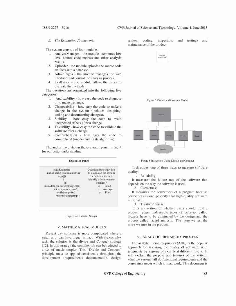
ISSN 2277 – 3916 CVR Journal of Science and Technology, Volume 4, June 2013
CVR College of Engineering 83
B. The Evaluation Framework
The system consists of four modules:
1. AnalyzeManager - the module computes low
level source code metrics and other analysis
results.
2. Uploader - the module uploads the source code
artifacts into a database.
3. AdminPages - the module manages the web
interface and control the analysis process.
4. EvalPages - the module allow the users to
evaluate the methods.
The questions are organized into the following five
categories:
1. Analyzability - how easy the code to diagnose
or to make a change.
2. Changeability - how easy the code to make a
change in the system (includes designing,
coding and documenting changes).
3. Stability - how easy the code to avoid
unexpected effects after a change.
4. Testability - how easy the code to validate the
software after a change.
5. Comprehension - how easy the code to
comprehend (understanding its algorithm).
The author have shown the evaluator panel in fig. 4
for our better understanding.
Evaluator Panel
classExample{
public static void main(string
args[])
{
int
num=Integer.parseInt(args[0]);
int temp=num,res=0;
while(temp>0){
res=res+temp;temp--;}
Question: How easy it is
to diagnoise the system
for deficiencies or to
identify where to make
changes?
o Good
o Average
o Poor
Figure. 4 Evaluator Screen
V. MATHEMATICAL MODELS
Present day software is more complicated where a
small error can have bigger impact. With the complex
task, the solution is the divide and Conquer strategy
[12]. In this strategy the complex job can be reduced to
a set of much simpler. This “Divide and Conquer”
principle must be applied consistently throughout the
development (requirements documentation, design,
review, coding, inspection, and testing) and
maintenance of the product
Figure 5 Divide and Conquer Model
Figure 6 Inspection Using Divide and Conquer
It discusses one of three ways to measure software
quality:
1. Reliability
It measures the failure rate of the software that
depends on the way the software is used.
2. Correctness
It measures the correctness of a program because
correctness is one property that high-quality software
must have.
3. Trustworthiness
It is a question of whether users should trust a
product. Some undesirable types of behavior called
hazards have to be eliminated by the design and the
process called hazard analysis. The more we test the
more we trust in the product.
VI. ANALYTIC HIERARCHY PROCESS
The analytic hierarchy process (AHP) is the popular
approach for assessing the quality of software, with
judgments by a group of experts at different levels. It
will explain the purpose and features of the system,
what the system will do functional requirements and the
constraints under which it must work. This document is

ISSN 2277 – 3916 CVR Journal of Science and Technology, Volume 4, June 2013
84 CVR College of Engineering
intended for the developer of software source code to
understand their code quality. To determine software
quality, quality metric models have been studied by
many researchers. The AHP selects six criteria with 27
sub criteria in ISO/IEC 9126-1 (2001), which is the
revision of 1991 version (ISO/IEC 9126, 1991) [13].
The relative rating provided by the expert contains nine
scale value i.e. Equally important, Weakly important,
Moderately important, Moderately plus, Strongly
important, Strongly plus, Very strongly, Very very
strongly and Extremely important. However the ratings
provided by the experts are all fuzzy numbers. The
proposed approach can help a group of various experts
including developers, testers and purchasers, to measure
the level of the software quality of the in-house
development or the third party development.
A. Prioritization Problem
Consider a 3*3 group pair wise matrix for 3 criteria
by 2 expert judgments as follows:
Phase 1: expert1 matrix
Step 1: consider 3 criteria given by only 1st expert from
the above matrix.
Step 2: consider only the lower values from the above
matrix (step 1).
Step 3: consider the higher values of the above
matrix(step 2) and calculate the Least Common
Multiple (LCM).
LCM=15
So the factors are 1*15, 3*5, 5*3, consider the upper
factors and add it i.e. 15+5+3=23.
Now calculate the reciprocal values
15/23= 0.652
5/23=0.217
3/23=0.130
Now the weighted matrix for lower values is
=
Step 4: calculate for medium values
Consider only the medium values from the above
matrix (step 1).
Step 5: consider the higher values of the above
matrix(step 4) and calculate the Least Common
Multiple (LCM).
LCM=12
So the factors are 1*12, 4*3, 6*2, consider the upper
factors and add it i.e. 12+3+2=17.
Now calculate the reciprocal values
12/17= 0.705
3/17=0.176
2/17=0.117
Now the weighted matrix for medium values is
=
Step 6: calculate for upper values
Consider only the upper values from the above matrix
(step 1).
Step 7: consider the higher values of the above matrix
(step 4) and calculate the Least Common Multiple
(LCM).
LCM=35
So the factors are 1*35,5*7, 7*5, consider the upper
factors and add it i.e. 35+7+5=47.
Now calculate the reciprocal values
35/47=0.744
7/47=0.148
5/47=0.106
Now the weighted matrix for upper values is
=
So the final weighted matrix for expert 1 is
=
Step 8: now divide the values with highest of upper
values i.e. 0.744

ISSN 2277 – 3916 CVR Journal of Science and Technology, Volume 4, June 2013
CVR College of Engineering 85
=
Now multiply the column values of the two matrixes
for the expert1
0.652*0.876 + 0.217*0.291 + 0.130*0.174= 0.657
0.705*0.947 +0.176*0.236 + 0.117*0.157= 0.726
0.744*1 + 0.148*0.198 + 0.106*0.142= 0.788
So the values for expert1 is
Phase 2: expert2 matrix
Step 1: consider 3 criteria given by only 2nd
expert from
the above matrix.
Step 2: consider only the lower values from the above
matrix (step 1).
Step 3: consider the higher values of the above
matrix(step 2) and calculate the Least Common
Multiple (LCM).
LCM=12
So the factors are 1*12, 2*6, 6*2, consider the upper
factors and add it i.e. 12+6+2=20.
Now calculate the reciprocal values
12/20= 0.6
6/20=0.3
2/20=0.1
Now the weighted matrix for lower values is
=
Step 4: calculate for medium values
Consider only the medium values from the above
matrix (step 1).
Step 5: consider the higher values of the above matrix
(step 4) and calculate the Least Common Multiple
(LCM).
LCM=21
So the factors are 1*21, 3*7, 7*3, consider the upper
factors and add it i.e. 21+7+3=31.
Now calculate the reciprocal values
21/31= 0.677
7/31=0.225
3/31=0.096
Now the weighted matrix for medium values is
=
Step 6: calculate for upper values
Consider only the upper values from the above matrix
(step 1).
Step 7: consider the higher values of the above matrix
(step 4) and calculate the Least Common Multiple
(LCM).
LCM=8
So the factors are 1*8, 4*2, 8*1, consider the upper
factors and add it i.e. 8+2+1=11.
Now calculate the reciprocal values
8/11=0.727
2/11=0.181
1/11=0.09
Now the weighted matrix for upper values is
=
So the final weighted matrix for expert 2 is
=
Step 8: now divide the values with highest of upper
values i.e. 0.727
=
Now multiply the column values of the two matrixes
for the expert2
0.6*0.825 + 0.3*0.412 + 0.1*0.137= 0.632
0.677*0.931 +0.225*0.309 + 0.096*0.132= 0.712
0.727*1 + 0.181*0.248 + 0.09*0.123= 0.782
So the values for expert2 is
Phase 3: Synthesis
The matrix values for expert1 is
And the matrix values for expert2 is
Now calculate the average of these two matrices

ISSN 2277 – 3916 CVR Journal of Science and Technology, Volume 4, June 2013
86 CVR College of Engineering
The final fuzzy value (0.644, 0.719, 0.785) is derived
as the level of the quality. These results the quality of
the new development is more than acceptable. Thus the
SQA can give permission for a product of this quality to
be used.
VII. CONCLUSION
We study various techniques approached by different
authors of software quality assurance to enable the
stakeholder for choosing right kind of techniques
suitable to their project. We also consider the in vivo
testing, in which tests are continuously executed in the
deployment environment. However, the technical
quality of source code (how well written it is) is an
important determinant for software maintainability. Our
survey focuses the low level source code metrics also
effect to the high level quality characteristics. One must
reconsider the divide and conquer principle applied
consistently throughout the development (requirements
documentation, design, review, coding, inspection, and
testing) and maintenance of the product. We conclude
the analytical hierarchy process is the best suitable
approach for software quality assurance.
REFERENCES
[1] P. McBreen, “Quality Assurance and Testing in Agile
Projects”, McBreen.Consulting, 2003.
[2] N. Zazworka et al., Investigating the Impact of Design
Debt on Software Quality, ACM 978-1-4503-0586-
0/11/05, pp. 17-23.
[3] C. Murphy et al., Quality Assurance of Software
Applications Using the In Vivo Testing Approach,
International Conference on Software Testing
Verification and Validation, IEEE DOI
10.1109/ICST.2009.18, 2009, pp. 111-120.
[4] R. Baggen et al., Standardized code quality benchmarking
for improving software maintainability, Software Qual J,
Springer Pub., DOI 10.1007/s11219-011-9144-9, 2012,
pp. 287–307.
[5] I. Heitlager et al., A practical model for measuring
maintainability, In proceedings of 6th international
conference on the quality of information and
communications technology (QUATIC 2007), IEEE
Computer Society, pp. 30–39.
[6] J. Correia et al., A survey-based study of the mapping of
system properties to iso/iec 9126 maintainability
characteristics, In 25th IEEE international conference on
software maintenance (ICSM 2009), September 20–26,
2009, pp. 61–70.
[7] J. P Correia, J. Visser, Certification of technical quality of
software products, In an International workshop on
foundations and techniques bringing together free/libre open source software and formal methods, FLOSS-FM
2008, pp. 35–51.
[8] P´eter Heged˝us, Tibor Bakota, L´aszl´o Ill´es, Gergely
Lad´anyi, Rudolf Ferenc, and Tibor Gyim´othy, Source
Code Metrics and Maintainability:A Case Study,
ASEA/DRBC/EL 2011, Springer-Verlag Berlin
Heidelberg 2011, CCIS 257, pp. 272–284.
[9] Bakota, T., Heged˝us, P., K¨ortv´elyesi, P., Rudolf, F.,
Gyim´othy, T., A Probabilistic Software Quality Model,
In Proceedings of the 27th IEEE International
Conference on Software Maintenance, ICSM 2011, IEEE
Computer Society, Williamsburg 2011, pp. 368–377.
[10] I. Heitlager, T. Kuipers, J. Visser, A Practical Model for
Measuring Maintainability, In Proceedings of the 6th
International Conference on Quality of Information and
Communications Technology, 2007, pp. 30–39.
[11] Bansiya, J., Davis, C., A Hierarchical Model for Object-
Oriented Design Quality Assessment, IEEE Transactions
on Software Engineering 28, 2002, pp. 4–17.
[12] David Lorge PARNAS, The use of mathematics in
software quality assurance, Front. Comput. Sci., Higher
Education Press and Springer-Verlag Berlin Heidelberg,
DOI10.1007/s11704-012-2904-2, 2012, pp. 3–16.
[13] K. K. F. Yuen, C.W. Lau Henry, A fuzzy group
analytical hierarchy process approach for software
quality assurance management, Fuzzy logarithmic least
squares method, Expert Systems with Applications 38,
ELSEVIER Publication, 2011, pp. 10292–10302.

ISSN 2277 – 3916 CVR Journal of Science and Technology, Volume 4, June 2013
CVR College of Engineering 87
Water Management Using Remote Sensing
Techniques
Mr. K.V Sriharsha1 and Dr. N.V Rao2 1CVR College of Engineering, IT Dept, Hyderabad, India
Email:[email protected]. 2
CVR College of Engineering, CSE Dept, Hyderabad, India
Email:[email protected]
Abstract--Water is the most conservative and natural
resource for agriculture. But unfortunately in our country
the well known fact is that the gap between the demand and
supply of water for agriculture is becoming larger. Due to
rapid increase in population growth, much of the water
resources are being diverted from agricultural to non
agricultural purposes. Instead of going into augmentation,
water management policies emphasize each and every
farmer to take an initiative in limiting water consumption
by implementing need based irrigation. To do so, a
systematic monitoring of water content at the surface of soil
and its root zone is essential at each stage of the growth of a
crop. In this process several methodologies like Gravimetric,
TDR, TDT, FDR, ADR, Phase Transmission and Nuclear
have evolved in determining soil moisture content and are
successful to some extent. These methods are chosen based
on factors like soil type, field maintenance, measurement
time, operating temperature, measurement range, accuracy,
power consumption, cost and ease of use. Information on
soil moisture can be obtained by using above techniques but
are time consuming and will have limited spatial coverage.
In that case Remote Sensing Techniques provide better
spatial and temporal coverage of soil moisture readings. The
role of electronics and computers in Agriculture in
designing sensors is very significant. This paper is limited to
remote sensing techniques in this respect.
Index terms—Remote Sensing, Electromagnetic Spectrum,
Hydrological Modeling, Soil Moisture Retrieval, Data
driven Modeling, Fresnel’s reflection coefficient,
brightness Temperature, and Root Mean Square Error.
I. INTRODUCTION
Remote sensing techniques are meant for observing
the earth’s surface or atmosphere using satellites (space
borne) or using aircrafts (airborne). Any information
about an object can be known without any physical
contact using electromagnetic energy in remote sensing
[1]. Whenever an electromagnetic energy radiation falls
on a surface, some of its energy will be absorbed or
transmitted and the rest is reflected. The sensing
devices (cameras, scanners, radiometers, radar etc) that
are mounted on aircrafts or satellites record the
electromagnetic energy that is reflected or emitted by
the earth’s surface. The information is recorded on
photographic films, videotapes or as digital data on
magnetic tapes. Different objects on earth’s surface
return different amount of energy at different
wavelengths in different bands of electromagnetic
spectrum. Sensors that are mounted on satellites or on
aircrafts take images of earth’s surface in various
wavelengths of electromagnetic spectrum. Wavelength
under which object reflects or emits radiation depends
on the property of material, surface roughness, angle
with which ray is incident on earth’s surface, intensity
and wavelength of radiant energy.
A. Stages in Remote Sensing
• Emission of electromagnetic radiation from
source
• Transmission of energy from source to surface
of the earth
• Electromagnetic energy interaction with the
earth’s surface (reflection and emission of EM
energy)
• Electromagnetic energy transmission from
surface of the earth to the sensor
• Recording of information from the reflected or
emitted electromagnetic energy in a specified
format by the optical sensors.
Regions of Electromagnetic Spectrum available for
Remote Sensing Systems are given in the following
table1.
B. Behavior of Electromagnetic Waves when Incident
on Vegetation crops, Soil and Water
• When an EM wave is incident on the vegetation,
chlorophyll in the leaves absorb the radiation in red
and blue wavelengths but reflect green wavelengths.
• When an EM wave incidents on the water, it is not
reflected instead it will be either absorbed or
transmitted.

ISSN 2277 – 3916 CVR Journal of Science and Technology, Volume 4, June 2013
88 CVR College of Engineering
• When an EM wave is incident on a soil surface, it
is either reflected or absorbed but only little will be
transmitted.
The reflectance property determines the characteristics
of the soil.
TABLE1
Regions of EM spectrum available for Remote Sensing [1]
II. Instruments used for remote sensing
A. Remote Sensors
Remote Sensor is an instrument that measure and
record electromagnetic energy.
Remote sensing instruments are categorized into two
types
• Passive Sensors
• Active Sensors
B. Passive Sensors
A passive sensor senses the electromagnetic radiation
that is emitted or reflected from an object from source
other than Sensor. According to Norman [2] these
sensors do not produce electromagnetic energy on their
own; instead depend on the external sources like Sun
and sometimes the earth. These sensors cover the
electromagnetic spectrum in a wavelength ranging from
less than 1 picometer (gamma rays) to greater than
1meter (microwaves).
From the irrigation perspective MICROWAVE
RADIOMETER is one of the most popular passive
sensor instrument that is used in soil moisture
estimation in the field. It is also used in mineral
exploration, snow and ice detection. This instrument
measures the intensity of radiation that is emitted or
reflected from the object within the microwave range
(0.1cm to 100cms). The depth from which energy is
emitted depends on the properties of the material such
as water content in the soil. The recorded
electromagnetic radiation is termed as brightness
temperature.
The other popular passive Sensor that comes in
discussion is Aerial Camera which is termed as airborne
sensor (a sensor used in aircrafts). Low orbiting
satellites and NASA space shuttle Mission use the
aerial Cameras for accurate navigation. Even Global
Navigation Satellite systems (GPS-USA) use the Aerial
camera systems to take the photographs of the objects
on the earth’s surface at precise points. Navigations are
most essential in survey areas where especially
topography maps won’t work. These sensors have film
which record the electromagnetic radiation in this
specified wavelength range (400nm-900nm).
The other popular passive remote Sensor is
Multispectral Scanner with which observations can be
made point by point and line by line manner. These
sensors can measure electromagnetic radiation in both
visible and infrared spectrum. These sensors can give
information about mineral compositions of the soil.
Imaging Spectrometer can measure intensity of
radiation in very narrow spectral bands (5nm-
10nm).These are used in determining chlorophyll
content of surface water.
Thermal Scanner measures the electromagnetic
radiation that falls within the specified range (8 micro
meters to 14 micrometers). The wavelength in this
range is related to temperature of the soil and hence
effects of droughts on agricultural crops can be studied.
The major disadvantage in passive remote sensing
systems is that they are sensitive to climatic conditions
especially when the sky is cloudy and the incoming
radiation cannot be sensed. To overcome this problem
Active remote sensing systems are used and they allow
the signal to pass through clouds, fog and rain.
C. Active Remote Sensing Systems
The most distinguishable feature of active sensor is
that they provide electromagnetic energy on their own
to illuminate the object on the earth’s surface. These
sensors also measure the electromagnetic radiation that
is emitted or reflected from the object. RADAR is one
of the well noted Active Remote Sensing systems
which can operate at microwave wavelength range. One
of the most popular radar is Synthetic Aperture Radar
[3].It transmits and receives the electromagnetic
radiation that fall within the microwave range (1mm to
1m). The electromagnetic energy that is emitted from
sensor can be penetrated into deeper parts in the soil
mantel and can be reflected from that point. This radar
system can be made to operate during daylight as well
as in darkness. These sensors give the knowledge of
deep and under canopy soil moisture.
Photographic
ultraviolet rays
0.3-0.4 micrometers Available for
remote sensing
Visible
0.4-0.4 micrometers Available for
remote sensing
Near and Mid
Infrared
0.7-3 micrometers
Available for
remote sensing
Thermal 3.0-14 micrometers Available for
remote sensing
microwave
0.1 to 100 cms
Available for
remote sensing and
can pass through
cloud, fog and rain
Radio
>100 cms
Not normally used
for remote sensing

ISSN 2277 – 3916 CVR Journal of Science and Technology, Volume 4, June 2013
CVR College of Engineering 89
RADARSAT is a popular Synthetic aperture radar
operate at 5 GHZ and is used worldwide in giving
response to disasters such as flooding, volcanic
eruptions and severe storms.
The other active remote sensing system is
ALTIMETER transmits microwave pulses and
measures round trip delay with which distance from
object to sensor is known. If the object is sea surface
then its height can be predicted and hence wind speed is
estimated. These sensors can be mounted on aircrafts
and satellites and can be used for topological mapping.
JASON-I is an altimeter which can provide the altitude
of earth’s ocean surface and is operated at frequencies
of 13.6GHz to 5.3GHz.
Scatterometers are the active sensors that measure
the back scattered radiation in microwave region and
derive the information about the wind direction and
speed over the earth’s surface with the help of the maps.
TABLE 2
Characteristics of Active Remote Sensing System
D. Measurement Principle
The emission of microwave energy is proportional to
the product of surface temperature and surface
emissivity [4]. Here the brightness of an emitter of a
microwave radiation is related to temperature of a
source through emissivity
TB is proportional to Teff
TB = (1-R)Teff = eTeff (1)
R- Directional Reflectivity of surface
Teff - Effective Radiation temperature
e- Effective emissivity = 1-R, which depends on
dielectric constant of medium and latter can be used to
determine soil moisture content.
E. Measuring Soil Moisture content using L Band
Radio Metric System
Microwave radiometer is one such Passive remote
sensing device measures the power level of the
incoming radiation. The power level (P) is expressed
based on the following relationship
P= K*Tb*B (2)
Tb is brightness temperature (defines the measure of
intensity of radiation at microwave frequencies)
K Boltzmann constant; B Bandwidth of the instrument
For a flat surface, Brightness temperature is
proportional to the physical temperature of the surface
as
Tb = e*T= (1-r) T (3)
e- Emissivity; r = Fresnel’s reflection coefficient
From Microwave Radiative Transfer Model [5] L-MEB
(L-Band Microwave Emission of Biosphere) the
brightness temperature (TBP) is expressed as
TBP = (1-wp)(1- p)(1+ prGp)Tc+(1-rGP) pTG (4)
Tc,TG - vegetative and effective soil temperatures.
rGP soil reflectivity
p vegetation attenuation factor
TBP polarized brightness temperature, where
p = e- p/cos
Is incident angle, p- vegetation optical depth
Soil reflectivity (rGP) depends on dielectric properties of
the soil such as permittivity, permeability, conductivity
etc which in turn depend on physical properties of soil
such as soil moisture, temperature, salinity and
geometric roughness.
Fresnel’s reflection coefficient(r) determines the
reflectance of the soil
r I (5)
• Small change in angle of incidence ( i<10oc)
exhibits small change in r values with variation
in dielectric properties of soil water mixture.
• Variation in soil moisture ( ) affects dielectric
properties of the soil ( , , f) which in turn
affects their value (reflection coefficients) and
in turn the difference in received power level
of the incoming radiation.
III. Analysis of Remotely Sensed Data Using
Hydrological Modeling Techniques
In order to perform analysis on remotely sensed data
such as soil moisture, hydrological models are mainly
used. These are further classified into two categories
namely physical based and empirical based. Physical
based modeling technique uses mathematical equations
derived from the system physical process. Hence it is
necessary to know about physical parameters in detail.
Especially in modeling the soil moisture component
characteristics SAR
(Synthetic
Aperture
radar)
Altimeter Scatterometer
Radiated
Power(W)
1500 20 100
Range(km)
695
1344
1145
Viewing
Geometry
Side looking
Nadir
looking
Six fan beam in
azimuth
Spectrum width
20-300MHz
320MHz
5-80KHz
Service Area
Land/coastal/
ocean
Ocean/ice
Ocean/ice/land

ISSN 2277 – 3916 CVR Journal of Science and Technology, Volume 4, June 2013
90 CVR College of Engineering
with respect to time and/or space, the physical
parameters like evapotransiration rate, infiltration rate,
percolation, soil type, and vegetation cover are to be
considered. The latter model which is empirical based
uses mathematical equations, derived from time series
data analysis. Without knowing explicitly the physical
behavior of the system one can use the Data Driven
Modeling (DDM). As the name implies it is based on
analysis of data about a system [6]. In particular, it
finds a way in relating system state variables (input and
output variables) without the physical behavior of
system , The model is trained on sample data of soil
moisture aiming at reducing the error which is shown as
difference between observed and predicted output.
A. Different Types of Data Driven Modeling
Techniques
Data Driven Modeling is classified into two
categories i.e. parameterized and non parameterized.
Recent survey on non parameterized data driven
modeling reveals the fact that statistical and Neural
Network modeling (NN) approaches are simple and
efficient in soil moisture retrieval.
B . Soil Moisture Retrieval using Statistical Approach
Support vector machines (SVM) and Relevance
vector machines (RVM) are supervised non parametric
statistical modeling techniques that are known for
producing desired estimations of soil moisture content
using inexpensive and readily available data. From the
experiments conducted at Walnet Creek Watershed in
Ames, South Central Iowa, USA, it is derived that
RVM model performs much better with RMSE of soil
moisture content depts. Of 5,10,20,30 and 50cm for
about 227 days. On the fourth day 1cm 0.014%v/v
compared to SVM whose RMSE value is 0.017%v/v
[7].
Their research starts with the development of three
models for soil moisture estimation. The first model
uses remotely sensed input consisting of meteorological
variables, field measurements and crop physiological
actors for training SVM and RVM models in order to
retrieve surface soil moisture at 0-6cms of top soil
layer. Once the model is trained, the soil moisture
content is estimated to check the model performance
with a RMSE value. The second model is trained with
inputs like soil temperature for 0-6 cms precipitation,
number of days last rained, including soil moisture
readings of model1 and surface soil moisture content at
30cm depth is estimated. The Model III is trained in
two steps. In the first step RVM and SVM models are
trained in a similar manner as Model I to estimate
surface soil moisture content. In the second step the
model is trained on remotely sensed data at a larger
scale to estimate soil moisture content at 30cms depth.
In order to measure the error between observed and
estimated data, the parameter, Root Mean Square Error
is used. The performance of a model is directly
proportional to the value of RMSE.
With reference to experimental study made on
Landsat images of study area superimposed with land
use in the year 2002, RMSE values obtained for soil
moisture retrieval at three models during training and
testing phases are tabulated as shown in table3.
TABLE 3.
RMSE values of soil Moisture Retrieval for SVM and RVM Models
[7]
SVM
RVM
Phases Training
phase
Testing
Phase
Training
Phase
Testing
Phase
Model 1 2.0%v/v 4.3%v/v 1.2%v/v 3.8%v/v
Model 2 0.36%v/v 0.66%v/v 0.02%v/v 0.48%v/v
Model 3 0.76%v/v 1.7%v/v 0.38%v/v 1.4%v/v
The results indicated in the table 3 show that RVM
model comparatively provides better performance in all
respects during training and test phases. This proves
that it has good potential of soil moisture estimation.
With reference to data taken from Soil climatic
Analysis network site at Rees centre, Texas, USA,
MVRM( Muitvariate Relevance Vector Machine)
trained on input variables like soil temperature, depth of
soil model, RMSE value for soil moisture retrieval is
recorded as 1.31% which indicate that observed data
and modeled values are close and model is performing
well. Even at the end of the 4th
day at a depth of 2mts,
RMSE reading is reduced to 0.15% which shows the
closeness of modeled value to the observed value
.Decrease in RMSE is a signature of good performance
of a model.
C. Soil Moisture Retrieval using Neural Network Model
A multilayer layered feed forward Artificial Neural
Network model used for research with input layer
consisting of selected input variables, a hidden layer
with ‘n’ number of hidden neurons and output layer
consisting of predicted soil moisture values. The
sigmoid and linear transfer functions are used in hidden
and output layers. The model uses an algorithm to train
the network. During forward phase the selected inputs
are propagated though the network from layer to layer.
An error is computed by comparing the difference
between desired and predicted output. This error is
propagated backwards and correspondingly weights and
bias are adjusted to minimize the error. The results of
the model show that with the appropriate selection of

ISSN 2277 – 3916 CVR Journal of Science and Technology, Volume 4, June 2013
CVR College of Engineering 91
inputs, the error is minimized and hence the accuracy in
soil moisture retrieval can be improved.
With reference to the National Airborne Field
Experiment 2005[8] conducted in Southern Australia
for Goulburn catchment, it is explicitly stated that the
near surface soil moisture measurements were taken
over eight farms at the same time by using active
remote sensing systems. The measurements were also
taken at many locations within a farm. For the study of
soil moisture estimation in a farm, a two layer
perceptron model consisting of 2 nodes in the input
layer, four neurons in the hidden layer and one at the
output layer is chosen. The model is trained with
several back propagation algorithms to adjust the
weights in the hidden and input layers so as to minimize
the root mean square error between actual and predicted
soil moisture output measurements. The results
obtained for RMSE are found to be between ranges of
3.93%v/v to 5.77%v/v, as shown in table 4.
In the table 4 it is explicitly stated that RMSE value
obtained after training the network with Quasi Newton
Algorithm-BFGS is comparatively less and this proves
that it is the only method that is capable of retrieving
soil moisture with the desired accuracy. TABLE 4
Root Mean Square Error (RMSE) of soil moisture retrieval for
various backpropogation algorithms [8]
sno Back Propogation algorithm
RMSE
(Root
Mean
Square
Error)%
v/v
1 Batch Gradient with Momentum 4.86
2 Gradient Descent with Adaptive Learning 4.88
3 Gradient descent with momentum and
adaptive learning rate 4.88
4 Resilient backpropogation 4.93
5 Conjugate gradient backpropogation with
Fletcher-Reeves updates 4.82
6 Conjugate gradient backpropogation Polak-
Ribiere updates 4.83
7 Conjugate gradient backpropogation with
Powell-Beale restarts 4.83
8 Scaled conjugate gradient backpropogation 5.77
9 Quasi-Newton Algorithm-BFGS 3.93
10 Quasi-Newton Algorithm: One step Secant
algorithm
5.51
11 Levenberg-Marquardt 4.04
D. Soil Moisture Retrieval using Classification and
Regression trees Algorithm (CART)
With reference to observations taken from
experimental study conducted at Yongdam Basin from
May 16th
to August 19th
, 2008[9], it is observed that use
of CART algorithm and neural networks provide proper
soil moisture field estimations and even represent soil
moisture behavior very well.
TABLE 5
RMSE values of soil moisture retrievals at four sites
For experimental study a neural network model was
built with input layer consisting of five nodes, hidden
layer consisting of five nodes and an output layer with
one node. The input variables to the model includes in
suite soil moisture measurements taken from Korean
water resources corporation (KWRC), precipitation ,
surface temperature provided by Korean Meteorological
Administration (KMA), Normalized Difference
Vegetation Index (NDVI) from Moderate Resolution
Imaging Spectro radiometer (MODIS).
IV. Irrisat- Water Management Service
Irrisat is an irrigation water management service uses
high level technology to deliver information to the
farmers. It was developed in New South Wales,
Australia by CSIRO Land and Water for collecting the
satellite images though remote sensing methods along
with the information from local weather stations and
sending the information to the farmers cell phones as an
SMS so that this would help the farmers to schedule
their irrigation at appropriate times [10]. The service
sends one SMS per day to each farmer who subscribes
the service. The whole system functions in such a way
that the light reflected from the vegetation and land
surface is captured by the remote sensors that are
mounted on satellites and are being processed using
software and hence crop vigor is extracted showing
evapotranspiration rate. At the same time from local
weather stations, farmers in different regions collect
data on temperatures, wind speed, solar radiation and
relative humidity and deliver the information to Irrisat
SMS database. The weather information combined with
satellite data determines the condition for actual water
consumption by crops on a particular farm. The Irrisat
service so far implemented successfully in Australia
and can even be implemented in Asian countries too
where cell phones are used extensively. Irrisat is a
promising service rough with which farmers will be
given a flexible irrigation management system meeting
their specific needs. In India, IFFCO SANCHAR
Limited has been offering services on IKSL Green SIM
CARD covering diverse areas including soil
management/crop production.
CONCLUSIONS
This review demonstrates the role of Remote Sensing in
Irrigation water Management. It is known that remotely
sensed data on soil moisture at larger scales can drive
the farmer to perform better water management
Area RMSE(%v/v)
Jucheon 1.3925
Bugui 1.0254
Sangjeon 1.8783
Ahncheon 1.0037

ISSN 2277 – 3916 CVR Journal of Science and Technology, Volume 4, June 2013
92 CVR College of Engineering
operations in scheduling the irrigation. A discussion has
been made on different instruments that perform remote
sensing, their characteristics and their applicability at
various types of soil. From the observations made on L
Band Radio Metric System, it is clearly noticed that the
difference in received level power level of incoming
radiation from the soil is an indicator of variation of soil
moisture content. It is mentioned that there are several
physical and data driven models that perform soil
moisture estimation. The survey on these models
reveals the fact that data driven modeling is one among
that is dominating in recent trends. It is to mention that
all over the world several countries including India, are
offering water management services to the farmers by
integrating remote sensing with mobile technology.
REFERENCES
[1] Baumann”Introduction To Remote Sensing”, State
university of Newyork, College at Oneonta, 2008.
[2] Bakker,Wimm ,”Principles Of Remote Sensing”,An
Introductory Textbook, 3rd Edition, Institute of Geo
information Sciences and Earth Observation.
[3] Huneycutt,”requency Use and needs of space borne active
sensors”, ,Geo Science and remote Sensing Symposium,
2000 proceedings,Pasadena,pp.2457-2463,2000.
[4] Jackson,”Surface Hydrology & Remote Sensing”, 1993.
[5] Philip,” Characteristics of Rape field Microwave Emission
and Implications of surface soil Moisture Retrieval”,
Remote Sensing,pp.247-270,2012.
[6] D. Solomantine, L.M See and R.J Abrahart,” Data Driven
Modeling: Concepts, Approaches and Experiences,
Practical Hydro informatics”, Water Science and
Technology Library68, Springer,2008.
[7] Bushra Zaman”,Remotely Sensed Data Assimilation
Technique to develop Machine Learning Model for use in
water Management”, Utah State University, Logan, Utah,
2010.
[8] Soo-See Chai,Bert Veenedaal,Geoff West,Jeffrey Philip
Walker,”Back Propogation Neural Network for soil
moisture retrieval using NAFE ’05 Data:A comparison of
different training algorithms”, University Of
Melbourne, International Archives of the Photgrammetry,
Remote Sensing and spatial Information Sciences,
Vol.XXXVII. Part B4, Beijing, 2008.
[9] Gwangseob Kim,Jung ,”Soil Moisture Estimaton using
Classification and Regression trees and neural networks,
,Geology and Continuum Mechanics,ISBN:978-960-474-
275-2,2009.
[10] Richard Soppe ,”Remote Sensing& Cell Phone
Technology deliver water management”, CSIRO Land
and Water, Dec1, 2010., Richard Soppe , CSIRO Land
and Water,Dec1,2010.

ISSN 2277 – 3916 CVR Journal of Science and Technology, Volume 4, June 2013
CVR College of Engineering 93
Health Hazards of Computer users &
Remedies (Computer Ergonomics) Dr.M.N.Ramakrishna M.D. A.F.I.H
Medical officer, CVR College of Engineering
Email:[email protected]
Abstract---Computer users, especially those who
continuously operate computers for hours together,
are usually prone to certain health problems which
are called ‘Musculo-Skeletal Disorders’ and
‘Computer Vision Syndrome. These problems can be
prevented to a large extent if users know a little about
‘Ergonomics’ of the computer. This article briefly
describes computer-related-disorders and ergonomic
tips for computer users.
Index Terms—Computer ergonomics, computer-
related disorders, Health Hazards
I. INTRODUCTION
Computers have become an integral part of life.
Newer studies show that if you don't use the
computer properly when working on a computer,
you chance discomfort, pain and even injury. New
research shows that it takes more than just an
ergonomic desk chair or a split keyboard to prevent
health problems affecting millions of computer
users. The repetitive motion is one factor among
many that contribute to a cluster of symptoms
called "computer-related disorder" (CRD).
A. Cumulative trauma disorder (CTD), and
Repetitive stress injury (RSI)
Work-related musculoskeletal system disorders
(WMSDs) are as follows.
1. Carpaltunnel syndrome
2. Back pain
3. Osteoarthritis
4. Tendinitis
5. Teno-synovitis
6. “Pitcher”,”Golfer” or”Tennis Elbow”
A. Computer Electromagnetic Radiation and
Its Health Effects
B. Computer Vision Syndrome
Some visual display users have reported sore and
tired eyes, blurred vision and eye fatigue after
prolonged use of their terminals. It is natural for
some people to experience visual discomfort if
they've been using their eyes intensively over a long
period of time, whether it is working at a display,
studying for an exam or doing close work. While
eye fatigue may be uncomfortable, it is not
damaging to the eye. It also is a temporary
condition and goes away with rest.
Most common work related Muscular skeletal
disorder is carpal Tunnel Syndrome which is
described below.
CARPAL TUNNEL SYNDROME
The carpal tunnel receives its name from the 8
bones in the wrist, called carpals that form a tunnel-
like structure. The tunnel is filled with flexor
tendons which control finger movement. It also
provides a pathway for the MEDIAN NERVE to
reach sensory cells in the hand. Repetitive flexing
and extension of the wrist may cause a thickening
of the protective sheaths which surround each of the
tendons. The swollen tendon sheaths, or Teno-
synovitis, apply increased pressure on the median
nerve and produce Carpal Tunnel Syndrome
MOTOR-Thenar muscle at the base of the thumb
atrophies and strength is lost.
SENSORY- Subjective or objective hypoesthesia
(decreased sensation) coinciding with median nerve
distributions, heat and cold sensation lost.
II. HELPFUL HINTS FOR WORK AREA
Millions of people work with computers every
day. There is no single “correct” posture or
arrangement of components that will fit everyone.
However, there are basic design goals to consider
when setting up a computer workstation or
performing computer-related tasks.
Creating the Ideal Computer Workstation
It is necessary to plan to create an ergonomically
sound workstation for computer users. The plan
should include illustrated guidelines on how to
adjust furniture, computer equipment, and work
aids. It must also include information on how to
organize work area and tasks, and checklists to
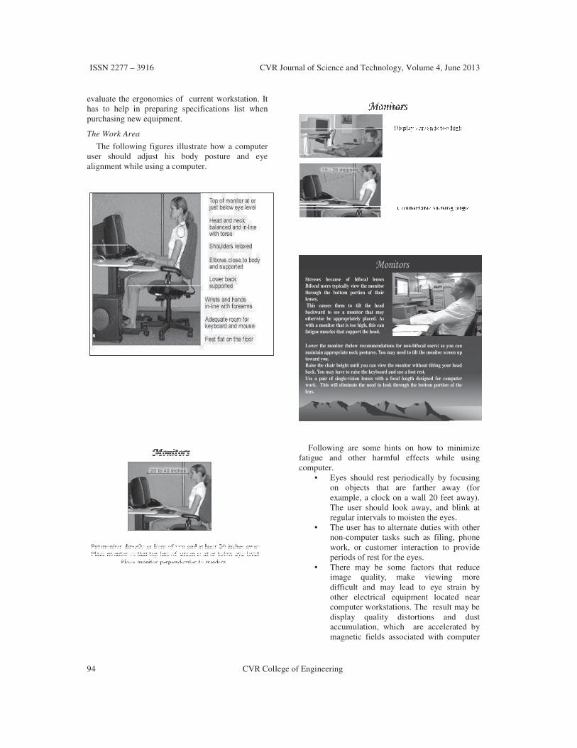
ISSN 2277 – 3916 CVR Journal of Science and Technology, Volume 4, June 2013
94 CVR College of Engineering
evaluate the ergonomics of current workstation. It
has to help in preparing specifications list when
purchasing new equipment.
The Work Area
The following figures illustrate how a computer
user should adjust his body posture and eye
alignment while using a computer.
Monitors
Stresses because of bifocal lenses
Bifocal users typically view the monitor
through the bottom portion of their
lenses.
This causes them to tilt the head
backward to see a monitor that may
otherwise be appropriately placed. As
with a monitor that is too high, this can
fatigue muscles that support the head.
Lower the monitor (below recommendations for non-bifocal users) so you can
maintain appropriate neck postures. You may need to tilt the monitor screen up
toward you.
Raise the chair height until you can view the monitor without tilting your head
back. You may have to raise the keyboard and use a foot rest.
Use a pair of single-vision lenses with a focal length designed for computer
work. This will eliminate the need to look through the bottom portion of the
lens.
Following are some hints on how to minimize
fatigue and other harmful effects while using
computer.
• Eyes should rest periodically by focusing
on objects that are farther away (for
example, a clock on a wall 20 feet away).
The user should look away, and blink at
regular intervals to moisten the eyes.
• The user has to alternate duties with other
non-computer tasks such as filing, phone
work, or customer interaction to provide
periods of rest for the eyes.
• There may be some factors that reduce
image quality, make viewing more
difficult and may lead to eye strain by
other electrical equipment located near
computer workstations. The result may be
display quality distortions and dust
accumulation, which are accelerated by
magnetic fields associated with computer

ISSN 2277 – 3916 CVR Journal of Science and Technology, Volume 4, June 2013
CVR College of Engineering 95
monitors. These may reduce contrast and
degrade viewing conditions.
• Computer workstations should be isolated
from other equipment that may have
electrostatic potentials in excess of +/- 500
volts.
• Computer monitors should be periodically
cleaned and dusted.
Additional hints are given below for using
related equipment with minimum discomfort.
Keyboards
• The keyboard should be directly in front of
the user.
• The user’s shoulders should be relaxed and
your elbows close to your body.
• The wrists should be straight and in-line
with your forearms
• Chair height and work surface height
should be adjusted to maintain a neutral
body posture.
• Elbows should be about the same height as
the keyboard and should hang comfortably
to the side of the body. Shoulders should
be relaxed, and wrists should not bend up
or down or to either side during keyboard
use.
• Central pencil drawers should be removed
from traditional desks if chair can not be
raised high enough because of contact
between the drawer and the top of the
thighs. The work surface should generally
be not more than 2 inches thick.
Pointer/Mouse
• The pointer/mouse should be kept close to
the keyboard.
• Both hands should be used alternately
while operating the pointer/mouse.
• Keyboard short cuts are to be used to
reduce strain.
Wrist/Palm Supports
• Wrist rest should be used to maintain
straight wrist postures and to minimize
contact stress during typing and mousing
tasks.
Document Holders
Documents should be at the same height
and distance as the monitor.
Chairs
Desirable specifications of computer chairs are:
• Adjustable chair and backrest
• Natural S-curvature of the spine
• Seat pan with a rounded, “waterfall” edge.
Shoulders in various positions are illustrated below.
Some other precautions are as follows:
• Taking micro breaks or rest pauses
• Adjusting to have optimum lighting
• Avoiding Glare Effect on monitor
III. ERGONOMIC TIPS FOR COMPUTER USERS
Ergonomics is “Study of how people physically
interact with their work, fitting the job, the
equipment and the work environment to the
worker”.
Ideal Office

ISSN 2277 – 3916 CVR Journal of Science and Technology, Volume 4, June 2013
96 CVR College of Engineering
• Head Up
• Shoulders relaxed
• Back erect and supported
• Eyes looking forward most of the time.
• Hands in line with the forearms.
• Only moderate pressure at the front of the
seat cushion
• Reference material is easy to look at.
• Feet firmly on a footrest.
• Monitor approximately at eye height and
an arms distance away.
Exercises for the office
One of the biggest injury risk factors is static
posture. This can be reduced by
• Spending at least 5 minutes every hour
away from your computer.
• Remembering to ONLY stretch to the
point of mild tension.
• Trying to incorporate the stretches into
daily routine.
Hand Exercises include
• Doing hand exercises like tight clenching
of hand into a fist and releasing it, fanning
out the fingers, and repeating it three
times.
Back and Shoulder Exercises
These include standing up straight, placing the right
hand on the left shoulder and moving head back
gently, and repeating it for the right shoulder.
Head and Neck Exercises
These involve
• Moving head sideways from left to right
and back to left.
• Moving head backward and then forward.
Computer and Desk Stretches
Sitting at a computer for long periods often
causes neck and shoulder stiffness and occasionally
lower back pain. This can be avoided by doing
following stretches every hour or so throughout the
day or whenever there is a feeling of stiffness. It
helps to get up and walk around the office every
now and then.
CONCLUSIONS
Many of the potential health problems associated
with using computers for long duration can be
avoided by following a few precautions and doing
appropriate physical exercises. The present article
has given an overview of these, and computer users
will benefit by making them a part of their work
culture.
Note: The information provided in this article is
collected from following websites.
www.cdc.gov/NIOSH
www.cdc.gov/
www.osha.gov/
www.ilo.org/
www.defense.gov/

ABOUT THE COLLEGE
CVR College of Engineering was established in 2001, and its ninth batch of students
graduated from the College. CVR is ranked among the top few of more than 600 colleges in AP
that started in the last decade and was also rated as the #1 co-educational college in Pass
percentage among nearly 300 colleges under JNTU, Hyderabad for examinations held in May
2009, November 2009 and May 2010. It is the expectation of the academic community that CVR
is on the successful path to be in the TOP-5 amongst all colleges in AP in the next few years.
The College was the first college in Osmania University area that was promoted by NRI
technology professionals resident in the US. The NRI promoters are associated with cutting-edge
technologies of the computer and electronics industry. They also have strong associations with
other leading NRI professionals working for world-renowned companies like IBM, Intel, Cisco,
Motorola, AT&T, Lucent and Nortel who have agreed to associate with the College with a vision
and passion to make the College a state-of-the-art engineering institution.
The College has been given permanent Affiliation and Autonomous status by JNTUH.
CALL FOR PAPERS:
Papers in Engineering, Science and Management disciplines are invited for
Publication in our Journal. Authors are requested to mail their contributions to Editor, CVR
Journal of Science and Technology (Email Id:[email protected]).
The Papers are to be written using a Standard Template, which may be obtained on
request from the Editor.