Embed Size (px)
Citation preview

ALL RIGHTS STRICTLY RESERVED. ANY PORTION OF THIS PAPER SHALL NOT BE REPRODUCED, COPIED, OR TRANSFORMED TO ANY OTHER FORMS WITHOUT PERMISSION FROM AU OPTRONICS CORP.
CUSTOMER APPROVAL SHEET
Company Name
MODEL
C070VW04 V6
CUSTOMER
APPROVED
Title :
Name :
□ APPROVAL FOR SPECIFICATIONS ONLY (Spec. Ver. 0.7 ) □ APPROVAL FOR SPECIFICATIONS AND ES SAMPLE (Spec. Ver.0.7 ) □ APPROVAL FOR SPECIFICATIONS AND CS SAMPLE (Spec. Ver.0.7 ) □ CUSTOMER REMARK :
1 Li-Hsin Rd. 2. Science-Based Industrial Park Hsinchu 300, Taiwan, R.O.C.
Tel: +886-3-500-8899 Fax: +886-3-577-2730
www.yslcd.com.tw

Version 0.7
Page: 2/18
ALL RIGHTS STRICTLY RESERVED. ANY PORTION OF THIS PAPER SHALL NOT BE REPRODUCED, COPIED, OR TRANSFORMED TO ANY OTHER FORMS WITHOUT PERMISSION FROM AU OPTRONICS CORP.
Doc. Version 0.7
Total Page 18
Date 2011/09/13
Product Specification
7" COLOR TFT-LCD MODULE
Model Name:::: C070VW04 V6
Planned Lifetime: From 2010/Jun To 2016/Jun
Phase-out Control: TBD
EOL Schedule: TBD
< >Preliminary Specification◆
< >Final Specification
Note: The content of this specif icat ion is subject to change .
© 2011 AU Optronics All Rights Reserved, Do Not Copy. ww
w.yslcd.com.tw
Version 0.7
Page: 3/18
ALL RIGHTS STRICTLY RESERVED. ANY PORTION OF THIS PAPER SHALL NOT BE REPRODUCED, COPIED, OR TRANSFORMED TO ANY OTHER FORMS WITHOUT PERMISSION FROM AU OPTRONICS CORP.
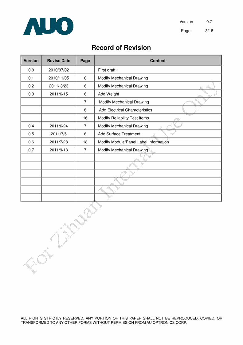
Record of Revision
Version Revise Date Page Content
0.0 2010/07/02 First draft.
0.1 2010/11/05 6 Modify Mechanical Drawing
0.2 2011/ 3/23 6 Modify Mechanical Drawing
0.3 2011/6/15 6 Add Weight
7 Modify Mechanical Drawing
8 Add Electrical Characteristics
16 Modify Reliability Test Items
0.4 2011/6/24 7 Modify Mechanical Drawing
0.5 2011/7/5 6 Add Surface Treatment
0.6 2011/7/28 18 Modify Module/Panel Label Information
0.7 2011/9/13 7 Modify Mechanical Drawing
www.yslcd.com.tw
Version 0.7
Page: 4/18
ALL RIGHTS STRICTLY RESERVED. ANY PORTION OF THIS PAPER SHALL NOT BE REPRODUCED, COPIED, OR TRANSFORMED TO ANY OTHER FORMS WITHOUT PERMISSION FROM AU OPTRONICS CORP.
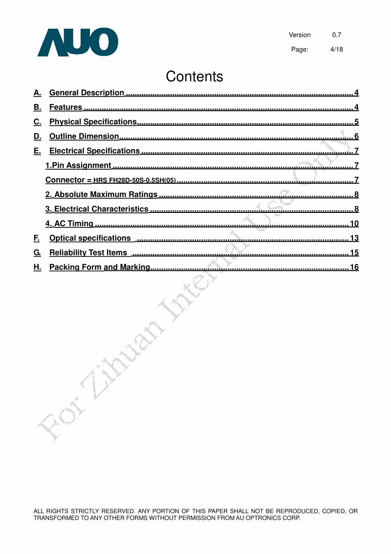
Contents A. General Description ....................................................................................................... 4
B. Features .......................................................................................................................... 4
C. Physical Specifications.................................................................................................. 5
D. Outline Dimension.......................................................................................................... 6
E. Electrical Specifications ................................................................................................ 7
1.Pin Assignment ............................................................................................................. 7
Connector = HRS FH28D-50S-0.5SH(05) ................................................................................ 7
2. Absolute Maximum Ratings ........................................................................................ 8
3. Electrical Characteristics ............................................................................................ 8
4. AC Timing ................................................................................................................... 10
F. Optical specifications ................................................................................................ 13
G. Reliability Test Items .................................................................................................. 15
H. Packing Form and Marking.......................................................................................... 16
www.yslcd.com.tw

Version 0.7
Page: 5/18
ALL RIGHTS STRICTLY RESERVED. ANY PORTION OF THIS PAPER SHALL NOT BE REPRODUCED, COPIED, OR TRANSFORMED TO ANY OTHER FORMS WITHOUT PERMISSION FROM AU OPTRONICS CORP.
A. General Description
C070VW04 V6 is an a-Si &Transmissive type Thin Film Transistor Liquid crystal Display
(TFT-LCD) with AMVA-Mobile (Advanced MVA) technology. This model is composed of a
TFT-LCD, a driver, an FPC (flexible printed circuit), and a backlight unit. TCON (timing
controller) is also embedded in source driver.
B. Features
� 7-inch (15:9) display
� 800RGB x 480 resolution in RGB stripe dot arrangement
� High brightness
� Interfaces: parallel RGB 18-bit
� Advanced MVA -- wide view technology
� RoHs compliance
www.yslcd.com.tw

Version 0.7
Page: 6/18
ALL RIGHTS STRICTLY RESERVED. ANY PORTION OF THIS PAPER SHALL NOT BE REPRODUCED, COPIED, OR TRANSFORMED TO ANY OTHER FORMS WITHOUT PERMISSION FROM AU OPTRONICS CORP.
C. Physical Specifications
NO. Item Unit Specification Remark
1 Display Resolution dot 800 RGB (H)×480(V)
2 Active Area mm 152.4(H)×91.44(V)
3 Screen Size inch 7(Diagonal)
4 Dot Pitch mm 0.0635(H)×RGBx0.1905(V)
5 Color Configuration -- R. G. B. Stripe Note 1
6 Color Depth -- 262K Colors
7 Overall Dimension mm 164.55(H) × 105.01(V) × 6.68(T) Note 2
8 Weight g 159.2+/-10%
9 Display Mode -- Normally Black
10 Surface Treatment -- AGAR
Note 1: Below figure shows dot stripe arrangement.
Note 2: Not including BOSS &FPC. Please refer to the drawing in page 6 for further information.
www.yslcd.com.tw

Version 0.7
Page: 7/18
ALL RIGHTS STRICTLY RESERVED. ANY PORTION OF THIS PAPER SHALL NOT BE REPRODUCED, COPIED, OR TRANSFORMED TO ANY OTHER FORMS WITHOUT PERMISSION FROM AU OPTRONICS CORP.
D. Outline Dimension
www.
yslcd
.com.
tw

Version 0.7
Page: 8/18
ALL RIGHTS STRICTLY RESERVED. ANY PORTION OF THIS PAPER SHALL NOT BE REPRODUCED, COPIED, OR TRANSFORMED TO ANY OTHER FORMS WITHOUT PERMISSION FROM AU OPTRONICS CORP.
E. Electrical Specifications 1. Pin Assignment Connector= HRS FH28D-50S-0.5SH(05)
No. Pin Name I/O Description Remarks
1 VCOM P Common electrode driving voltage 2 VGH P Positive power supply voltage for TFT
3 VGL P Negative power supply voltage for TFT
4 VDD P Digital power supply voltage.
5 GND G Ground
6 V1 I Gamma correction voltage
7 V2 I Gamma correction voltage
8 V3 I Gamma correction voltage
9 V4 I Gamma correction voltage
10 V5 I Gamma correction voltage
11 V6 I Gamma correction voltage
12 V7 I Gamma correction voltage
13 V8 I Gamma correction voltage
14 V9 I Gamma correction voltage
15 V10 I Gamma correction voltage
16 V11 I Gamma correction voltage
17 V12 I Gamma correction voltage
18 V13 I Gamma correction voltage
19 V14 I Gamma correction voltage
20 AVDD P Analog power supply voltage
21 AVDD P Analog power supply voltage
22 GND G Ground
23 DE I Data enable Input (High active)
24 DCLK I Data clock Input
25 GND G Ground
26 DB5 I Blue data input(MSB)
27 DB4 I Blue data input
28 DB3 I Blue data input
29 DB2 I Blue data input
30 DB1 I Blue data input
31 DB0 I Blue data input(LSB)
32 DG5 I Green data input (MSB)
33 DG4 I Green data Input
34 DG3 I Green data Input
35 DG2 I Green data Input
36 DG1 I Green data Input
37 DG0 I Green data Input (LSB)
38 DR5 I Red data input (MSB)
39 DR4 I Red data input
40 DR3 I Red data Input
41 DR2 I Red data Input
42 DR1 I Red data Input
43 DR0 I Red data Input (LSB)
44 GND G Ground
45 SHLR I
Horizontal scan direction control. “H”�Left to Right; “L”�Right to Left
46 UPDN I
Vertical scan direction control. “H”�Down to Up; “L”�Up to Down
47 STBYB I
Standby mode. "H" for normal operation. "L" for standby mode.
48 RSTB I Global reset pin. (low active)
www.yslcd.com.tw

Version 0.7
Page: 9/18
ALL RIGHTS STRICTLY RESERVED. ANY PORTION OF THIS PAPER SHALL NOT BE REPRODUCED, COPIED, OR TRANSFORMED TO ANY OTHER FORMS WITHOUT PERMISSION FROM AU OPTRONICS CORP.
49 GND G Ground
50 V-COM P Common electrode driving voltage
I: Digital signal input, O: Digital signal output, G: GND, P: Power input
2. Absolute Maximum Ratings Values
Items Symbol Min. Max.
Unit Condition
VDD -0.3 4.5 V
AVDD -0.5 13.5 V
VGH -0.3 20 V
VGL -15 0.3 V
Power Voltage
VGH-VGL 0 35 V
Vi -0.3 Vdd+ 0.3 V
Vref(V1~V7) 0.4AVDD AVDD-0.3 V
Vref(V8~V14) 0.1 0.6AVDD V Input Signal Voltage
VCOM -0.3 10 V
Operation Temperature Topa -30 +85 ℃ Ambient
Storage Temperature Tstg -40 +95 ℃ Ambient
Vf -0.5 24 V LED
If 0 85 mA
Note 1: Functional operation should be restricted under normal ambient temperature.
3. Electrical Characteristics The following items are measured under stable condition and suggested application circuit.
a. TFT- LCD Panel
Parameter Symbol Min Typ Max Unit Notes
VDD 3.1 3.3 3.5 V
IVDD -- 6.7 8.7 mA
AVDD V1+0.1 12.5 12.8 V
IAVDD - 26 34 mA
VGH 14.5 15 15.5 V
IVGH - 0.15 0.2 mA
VGL -9.5 -9 -8.5 V
IVGL - 0.2 0.3 mA
VCOM 5.22 5.42 5.62 V
Power Supply
IVCOM - 0.3 0.65 uA
Vi -0.3 - Vdd+ 0.3 V
Vref(V1~V7) 0.4AVdd - AVdd-0.3 V Input Signal Voltage Vref(V8~V14) 0.1 - 0.6AVdd V
Input high voltage Vh 0.7Vdd - Vdd V
Input low voltage Vl 0 - 0.3Vdd
Vertical cycle fV 50 60 80 Hz
Horizontal cycle fH 28.9 31.5 42 kHz
Dot Frequency fDCLK 33.3 45 MHz
b. Recommend Gamma Voltage
Parameter Symbol Min Typ Max Unit Notes
V1 - 12.23 - V
V2 - 11.70 - V
Gamma Voltage
V3 - 10.46 - V
www.yslcd.com.tw

Version 0.7
Page: 10/18
ALL RIGHTS STRICTLY RESERVED. ANY PORTION OF THIS PAPER SHALL NOT BE REPRODUCED, COPIED, OR TRANSFORMED TO ANY OTHER FORMS WITHOUT PERMISSION FROM AU OPTRONICS CORP.
V4 - 9.84 - V
V5 - 9.41 - V
V6 - 8.65 - V
V7 - 6.80 - V
V8 - 6.40 - V
V9 - 4.45 - V
V10 - 3.68 - V
V11 - 3.16 - V
V12 - 2.49 - V
V13 - 1.07 - V
V14 - 0.27 - V
c. Backlight Driving Conditions (Note 1)
Parameter Symbol Min. Typ. Max. Unit Remark
LED Supply Current
IL - 80 85 mA single serial
(Note 3)
LED Supply Voltage
VL - 21 24 V Note 3,25゚C
LED Life Time LL 10000 --- --- Hr Note 2
Note 1: LED backlight is 18 LEDs (3 strings, 6pcs for each string). Note 2: The LED lifetime 10000hrs means , after normal use at 80mA, under +25 ゚ C, the brightness
decreases to 50% of original level.
Note 3: The LED supply power is for 3 string of LED Note 4: The voltage capacity of LED driver IC must be over max. of LED Voltage.
www.yslcd.com.tw

Version 0.7
Page: 11/18
ALL RIGHTS STRICTLY RESERVED. ANY PORTION OF THIS PAPER SHALL NOT BE REPRODUCED, COPIED, OR TRANSFORMED TO ANY OTHER FORMS WITHOUT PERMISSION FROM AU OPTRONICS CORP.
4. AC Timing
a. Power on/off sequence The LCD adopts high voltage driver IC, so it could be permanently damaged under a
wrong power on/off sequence. The suggested LCD power sequence is below: Power on sequence: VDD -> GRB -> STBYB -> Digital input (Data/DCLK/DE) -> AVDD -> VGL -> VGH -> BLKEN
Power-Off STBYB -> BLKEN -> AVDD -> VGH -> VGL -> Digital input (Data/DCLK/DE)& VDD
`
DEN : Defined a frame period and created internally by DE. It is similar vertical sync.
GRB : Global reset ,normally pulled high. Suggest to connecting with an RC reset circuit for stability .Normally pull high.
STBYB : Standby mode, normally pulled high. STBYB ="1" , normal operation STBYB="0",timing controller, source driver will turn off, all output are High-Z
www.yslcd.com.tw
Version 0.7
Page: 12/18
ALL RIGHTS STRICTLY RESERVED. ANY PORTION OF THIS PAPER SHALL NOT BE REPRODUCED, COPIED, OR TRANSFORMED TO ANY OTHER FORMS WITHOUT PERMISSION FROM AU OPTRONICS CORP.
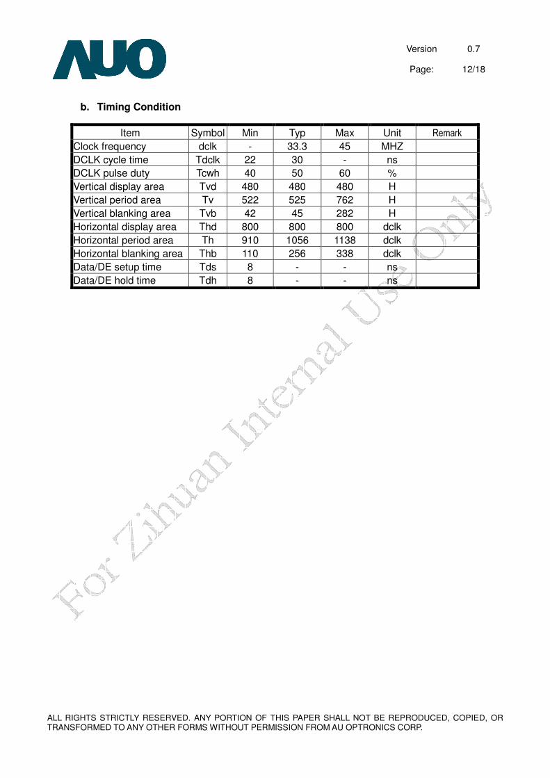
b. Timing Condition
Item Symbol Min Typ Max Unit Remark
Clock frequency dclk - 33.3 45 MHZ
DCLK cycle time Tdclk 22 30 - ns
DCLK pulse duty Tcwh 40 50 60 %
Vertical display area Tvd 480 480 480 H
Vertical period area Tv 522 525 762 H
Vertical blanking area Tvb 42 45 282 H
Horizontal display area Thd 800 800 800 dclk
Horizontal period area Th 910 1056 1138 dclk
Horizontal blanking area Thb 110 256 338 dclk
Data/DE setup time Tds 8 - - ns
Data/DE hold time Tdh 8 - - ns
www.yslcd.com.tw
Version 0.7
Page: 13/18
ALL RIGHTS STRICTLY RESERVED. ANY PORTION OF THIS PAPER SHALL NOT BE REPRODUCED, COPIED, OR TRANSFORMED TO ANY OTHER FORMS WITHOUT PERMISSION FROM AU OPTRONICS CORP.
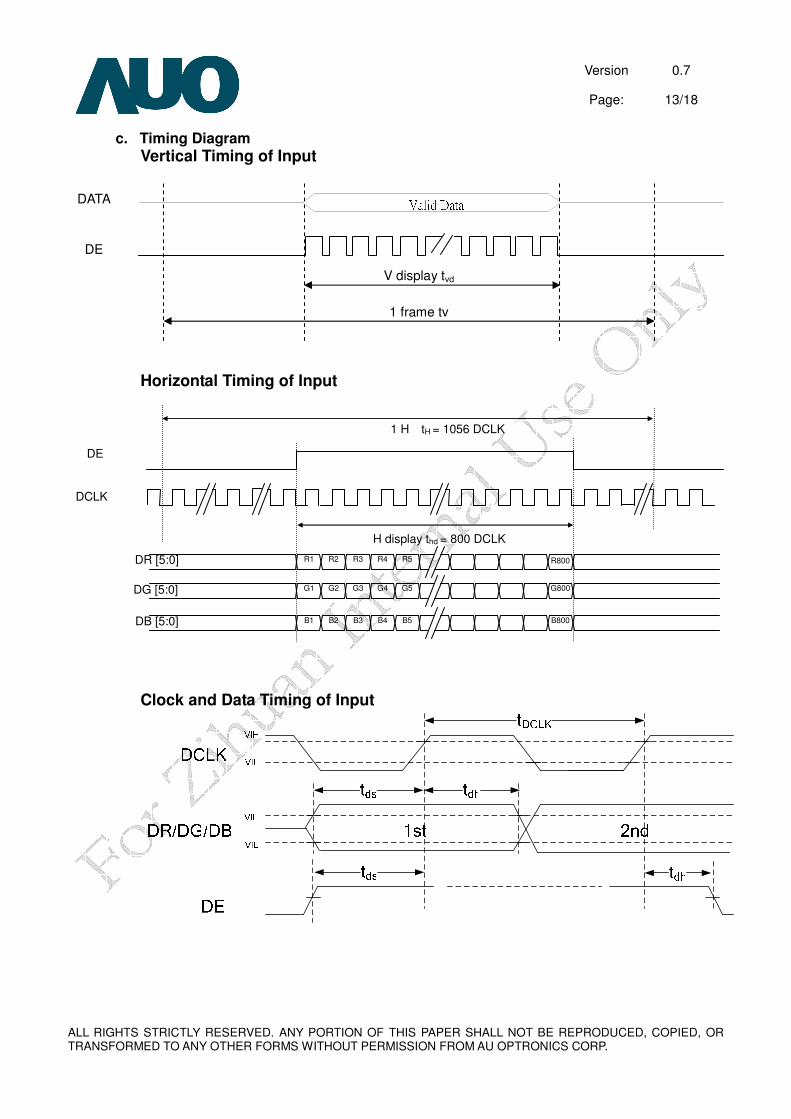
c. Timing Diagram
Vertical Timing of Input
Horizontal Timing of Input
Clock and Data Timing of Input
DE
DCLK
DR [5:0]
DG [5:0]
DB [5:0]
H display thd = 800 DCLK
1 H tH = 1056 DCLK
R1 R2 R3 R4 R5 R800
B1 B2 B3 B4 B5 B800
G1 G2 G3 G4 G5 G800
DATA
DE
Valid Data
1 frame tv
V display tvd
www.yslcd.com.tw
Version 0.7
Page: 14/18
ALL RIGHTS STRICTLY RESERVED. ANY PORTION OF THIS PAPER SHALL NOT BE REPRODUCED, COPIED, OR TRANSFORMED TO ANY OTHER FORMS WITHOUT PERMISSION FROM AU OPTRONICS CORP.
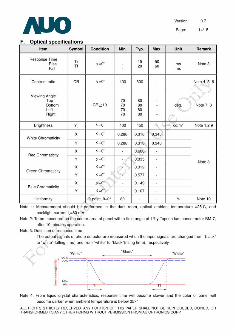
F. Optical specifications
Item Symbol Condition Min. Typ. Max. Unit Remark
Response Time Rise Fall
Tr Tf
θ=0° - -
15 20
50 60
ms ms
Note 3
Contrast ratio CR θ=0° 400 600 - Note 4, 5, 6
Viewing Angle Top Bottom Left Right
CR≧10
70 70 70 70
80 80 80 80
- - - -
deg. Note 7, 8
Brightness YL θ=0° 400 450 - cd/m2 Note 1,2,9
X θ=0° 0.288 0.318 0.348 White Chromaticity
Y θ=0° 0.288 0.318 0.348
X θ=0° - 0.600 - Red Chromaticity
Y θ=0° - 0.335 -
X θ=0° - 0.312 - Green Chromaticity
Y θ=0° - 0.577 -
X θ=0° - 0.149 - Blue Chromaticity
Y θ=0° - 0.107 -
Note 8
Uniformity 9-point, θ=0° 80 - - % Note 10
Note 1: Measurement should be performed in the dark room, optical ambient temperature =25°C, and
backlight current IL=80 mA
Note 2: To be measured on the center area of panel with a field angle of 1°by Topcon luminance meter BM-7,
after 10 minutes operation.
Note 3: Definition of response time:
The output signals of photo detector are measured when the input signals are changed from “black”
to “white”(falling time) and from “white” to “black”(rising time), respectively.
Sig
nal(R
ela
tive v
alu
e)
"Black"
Tr Tf
"White""White"
0%10%
90%100%
Note 4. From liquid crystal characteristics, response time will become slower and the color of panel will
become darker when ambient temperature is below 25℃.
www.yslcd.com.tw

Version 0.7
Page: 15/18
ALL RIGHTS STRICTLY RESERVED. ANY PORTION OF THIS PAPER SHALL NOT BE REPRODUCED, COPIED, OR TRANSFORMED TO ANY OTHER FORMS WITHOUT PERMISSION FROM AU OPTRONICS CORP.
Note 5. Contrast ratio is calculated with the following formula.
Note 6. White Vi=Vi50 m 1.5V
Black Vi=Vi50 ± 2.0V
“±” means that the analog input signal swings in phase with COM signal.
“ m ” means that the analog input signal swings out of phase with COM signal.
Vi50 :The analog input voltage when transmission is 50%
The 100% transmission is defined as the transmission of LCD panel when all the input terminals of
module are electrically opened.
Note 7. Definition of viewing angle: refer to figure as below.
Note 8. The viewing angles are measured at the center area of the panel when all the input terminals of LCD
panel are electrically opened.
Note 9. Brightness is measured at the center of the display with white pattern in 80mA
Note 10. Luminance Uniformity is defined as following within the 9 measurements (L1~L9),
Luminance Uniformity(%) =Minimum luminance(brightness)/Maximum luminance(brightness)
state Black"" at is LCD whenoutput detector Photo
state White"" at is LCD whenoutput detector PhototioContrastra =
www.yslcd.com.tw

Version 0.7
Page: 16/18
ALL RIGHTS STRICTLY RESERVED. ANY PORTION OF THIS PAPER SHALL NOT BE REPRODUCED, COPIED, OR TRANSFORMED TO ANY OTHER FORMS WITHOUT PERMISSION FROM AU OPTRONICS CORP.
G. Reliability Test Items
No. Test items Conditions Remark
1 High temperature storage Ta= 95℃ 240Hrs
2 Low temperature storage Ta= -40℃ 240Hrs
3 High temperature operation Ta= 85℃ 240Hrs
Note1
4 Low temperature operation Ta= -30℃ 240Hrs Note1, 3
5 High temperature and high
humidity Ta= 60 , 90% RH℃ 240Hrs Operation
6 Heat shock -30 ~85 /100℃ ℃ cycles 1Hrs/cycle Non-operation
7 Electrostatic discharge
Contact = ± 8 kV, class B (R=330Ω,C=150pF)
Air = ± 15 kV, class B (R=330Ω,C=150pF)
,10 times for each terminal
Operation (Note 4)
Frequency range 8~33.3Hz
Stoke 1.3mm
Sweep 2.9G, 33.3~400Hz
Cycle 15min.
8 Vibration
2 hours for each direction of X, Z 4 hours for Y direction
JIS D1601,A10 Condition A
9 Mechanical shock 100G, 6ms, ±X,±Y,±Z
3 times for each direction
10 Vibration (with carton) Random vibration:
0.015G2/Hz from 5~200Hz
–6dB/Octave from 200~500Hz IEC 68-34
11 Drop (with carton) Height: 60cm
1 corner, 3 edges, 6 surfaces
Note 1: Ta: Ambient temperature. Note 2: In the standard condition, there is not display function NG issue occurred. All the cosmetic
specification is judged before the reliability stress. Note 3: Short time operation between -40℃~-30℃ doesn't provide full performance but a correct image
on the LCD. The LCD is guaranteed to suffer no permanent damage. Note 4: Test techniques follow IEC61000-4-2 standard www.yslcd.com.tw

Version 0.7
Page: 17/18
ALL RIGHTS STRICTLY RESERVED. ANY PORTION OF THIS PAPER SHALL NOT BE REPRODUCED, COPIED, OR TRANSFORMED TO ANY OTHER FORMS WITHOUT PERMISSION FROM AU OPTRONICS CORP.
H. Packing Form and Marking 1. Packing Form
www.yslcd.com.tw

Version 0.7
Page: 18/18
ALL RIGHTS STRICTLY RESERVED. ANY PORTION OF THIS PAPER SHALL NOT BE REPRODUCED, COPIED, OR TRANSFORMED TO ANY OTHER FORMS WITHOUT PERMISSION FROM AU OPTRONICS CORP.
2. Module/Panel Label Information The module/panel (collectively called as the “Product”) will be attached with a label of Shipping Number
which represents the identification of the Product at a specific location. Refer to the Product outline drawing for detailed location and size of the label. The label is composed of a 22-digit serial number with the following definition:
Example: 501M06ZL06123456781Z05: Product Manufacturing Week Code: WK50 Product Version: Version 1 Product Manufacturing Factory: L3A (The manufacturing site at Taiwan) Note: 1. M06: The manufacturing site in Taiwan 2. S16: The manufacturing site in Xiamen
PS. In order to avoid mix material , the modle name printed on module label will change from C070VW04 V6 to C070VW04 V61.
3. Carton Label Information The packing carton will be attached with a carton label where packing Q’ty, AUO Model Name, AUO Part
Number, Customer Part Number (Optional) and a series of Carton Number in 13 or 14 digits are printed. The Carton Number is appearing in the following format:
Refer to the drawing of packing format for the location and size of the carton label.
www.yslcd.com.tw


