Embed Size (px)
Citation preview

www.altium.com 1
CUSTOM FOOTPRINT CREATION GUIDE FOR AD

www.altium.com 1
CUSTOM FOOTPRINT CREATION GUIDE FOR AD
WHY CUSTOM FOOTPRINTS? .............................................................................................................................................................................................................................................................2
WHAT A GOOD FOOTPRINT SHOULD LOOK LIKE? ..............................................................................................................................................................................3
WHAT IS OPTIONAL BUT NOT NECESSARY? .....................................................................................................................................................................................................5
METHODOLOGY ..............................................................................................................................................................................................................................................................................................................5
Part and Pad Decomposition ........................................................................................................................................................................................................................................................5
Mechanical Snaps ...............................................................................................................................................................................................................................................................................................5
Building Guide ..........................................................................................................................................................................................................................................................................................................7
CONCLUSIONS ..................................................................................................................................................................................................................................................................................................................9
APPENDIX A: MAKING A PROPORTIONAL COURTYARD ..........................................................................................................................................................9
APPENDIX B: SNAPPING A COMPLEX 3D MODEL ....................................................................................................................................................................................9
APPENDIX C: SOLID REGIONS FOR COMPLEX PAD SHAPES .......................................................................................................................................10
APPENDIX D: USING SLOT HOLES INSTEAD OF ROUND HOLES ..........................................................................................................................10
www.altium.com 2
CUSTOM FOOTPRINT CREATION GUIDE FOR AD
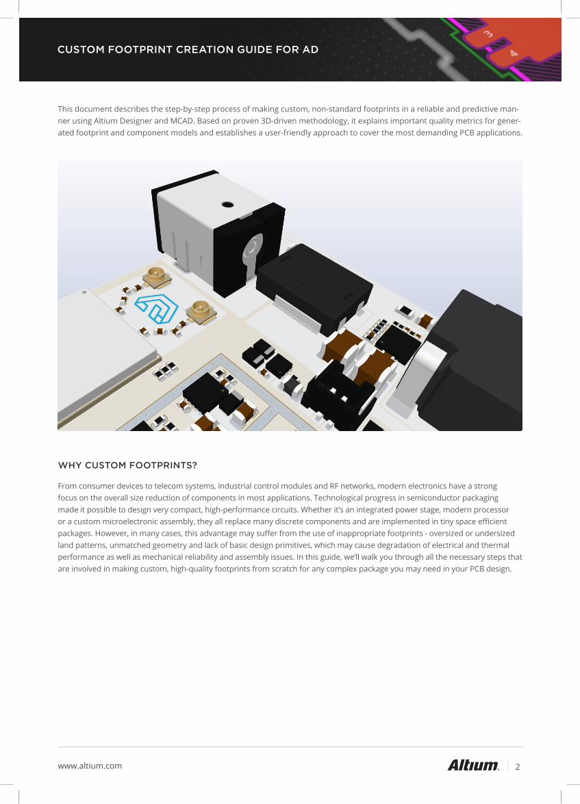
This document describes the step-by-step process of making custom, non-standard footprints in a reliable and predictive man-ner using Altium Designer and MCAD. Based on proven 3D-driven methodology, it explains important quality metrics for gener-ated footprint and component models and establishes a user-friendly approach to cover the most demanding PCB applications.
WHY CUSTOM FOOTPRINTS?
From consumer devices to telecom systems, industrial control modules and RF networks, modern electronics have a strong focus on the overall size reduction of components in most applications. Technological progress in semiconductor packaging made it possible to design very compact, high-performance circuits. Whether it’s an integrated power stage, modern processor or a custom microelectronic assembly, they all replace many discrete components and are implemented in tiny space efficient packages. However, in many cases, this advantage may suffer from the use of inappropriate footprints - oversized or undersized land patterns, unmatched geometry and lack of basic design primitives, which may cause degradation of electrical and thermal performance as well as mechanical reliability and assembly issues. In this guide, we’ll walk you through all the necessary steps that are involved in making custom, high-quality footprints from scratch for any complex package you may need in your PCB design.

www.altium.com 3
CUSTOM FOOTPRINT CREATION GUIDE FOR AD
- Accurate component pads
Using either oversized or undersized pads is a common issue for lots of non-standard components. Sometimes pads are split in very odd manners or they don’t represent actual package pins.
In this document, we’ll use a simple decomposition tech-nique which allows you to build any part using a very intui-tive and simple approach.
While 3D model is essential because it checks the footprint and vice versa, in this document we’ll describe how to build, modify and maintain stable, fault-free, high-quality 3D mod-els which are both detailed and light.
WHAT A GOOD FOOTPRINT SHOULD LOOK LIKE?
- Accurate 3D model
There are plenty of free 3D models available on the Internet, however, not all of them are worth using. Most of them are not optimized for ECAD (model size is too large) or they’re oversimplified in such a manner that it makes almost no dif-ference between said model and “grey brick”. Models made by enthusiasts are very often inaccurate, faulty, and they often suffer from a lack of correctly applied methodology.

www.altium.com 4
CUSTOM FOOTPRINT CREATION GUIDE FOR AD
- Accurate mechanical outline
Serving as the component body projection onto the PCB surface, this flat geometry data plays an important role in representing the area that component bodies share once placed.
- Accurate courtyard
Being one of the most overlooked and underestimated subjects in the PCB world, as many designers don’t use it, the courtyard provides extremely valuable data for correct component placement.
The reason why the courtyard is not only very important but extremely useful and handy in PCB design is the fact that it serves as the natural boundary of the overall footprint area. It allows you to place components with the highest level of density that can be achieved - this is obviously court-yard-to-courtyard edge placement.
It’s exactly that “border”, which clearly shows you the existing headroom for the components position and completely defines the absolute minimum area shared by components while surrounded by neighbor components and/or any other physical/electrical obstacles. In this guide, we’ll use a proportional courtyard, which accurately represents the total footprint’s placement area without dead zones.

www.altium.com 5
CUSTOM FOOTPRINT CREATION GUIDE FOR AD
WHAT IS OPTIONAL BUT NOT NECESSARY?
Depending on used methodology or standards, as well as design-driven constraints, these optional subjects may or not be presented in particular designs without any impact on footprints quality:
� Silkscreen marking
� Designator on the mechanical layer
� Additional graphics/text
In this document, we won’t cover the above mentioned subjects, however, there is some additional data provided in the appendix.
METHODOLOGY
Part and Pad Decomposition
If we temporarily remove that big exposed pad shortening the upper row of pads this package will turn into a standard one, which will be supported by many existing calculators and footprint wizards - Small Outline No-Led(SON). Once we calculate all the pads it becomes possible to combine them into a target footprint and proceed with final tuning. More-over, complex footprints may already have only simple pads but with specific placement - that means you can deconstruct an entire part into relatively small and simple ones. Let’s take a look at the u.fl connector.
Simply put, it’s a method of extracting relatively simple pads from complex ones in such a manner that allows accurate calculation of geometry for any simple pad independently using either built-in or external calculators. Let’s have a look.
Mechanical Snaps
3D model
On one hand, a good 3D model should be accurate and detailed in a reasonable manner to serve as a good representation of the real device, but on the other, it should be lightweight and easy to use. To achieve that some key directions should be followed:
It can be deconstructed into two simple parts which are represented by the Small Outline Diode Flat Lead(SODFL) package.
One of the biggest advantages of this technique is the possibility to apply IPC rules (and thus Density Level settings) to complex parts by applying these rules to their corresponding subparts made during deconstruction.

www.altium.com 6
CUSTOM FOOTPRINT CREATION GUIDE FOR AD
- The part should only be represented by a solid body, and not by a set/assembly of multiple solid bodies and/or sur-faces with intersections. If the usage of assemblies can’t be avoided, try to reduce the number of corresponding sub-parts as much as possible by combining bodies of suitable subparts at the MCAD level.
- All markings made by laser or painting should be done with surface cutting tools, like split line instead of cut or boss extrude. Using cut or boss extrude might dramatically increase the model size and this very often leads to faulty behavior and artifacts when imported even into ECAD during the meshing process.
- Usage of arcs, rounded corners, and surfacing tech-niques should be minimized to avoid unnecessary over detailing, which will cause the same problems as in the previous example.
- Your CAD tool used for making the model should be capable of generating high-quality step models without any drawbacks related to its architecture or tool implementation. For example, STEP files generated in Solidworks in almost all cases will have overwhelming size, faulty surfaces (especially if split line tool is used) and dropped colors, while those models made in Inventor are just fine. Moreover, it’s not an uncommon situation when STEP models made originally in Solidworks suffer from the previ-ously mentioned problems during import. At the moment Inventor seems to have the greatest STEP editing and import/export capabilities among professional MCAD packages.
Eventually, you should take the time to ensure that the tool works reliably and there is no garbage info, duplicated surfaces, or visual artifacts in your model.

www.altium.com 7
CUSTOM FOOTPRINT CREATION GUIDE FOR AD
Building Guide
1. Start from 3D modeling
If there is a manufacturer’s original model with sufficient quality you can use it. In the opposite case, you may need to heal or even restore the missing geometry, and of course, build your own, which is the best option in many cases.
2. Proceed with the first geometry analysis
Check if that 3D model is a perfect match with the man-ufacturer drawings and manufacturer recommended footprint (if available) - complex parts may have incorrect or missing drawings, dimensions, etc.
3. Deconstruct the components package and/or pads into generic ones
When a target part has pads with simple shapes it’s pos-sible to represent it as a set of simple standard packages. In the case of complex shapes, you’ll need to deconstruct those into standard pads first.
4. Calculate pad geometry for each generic subpart created
For each subpart, use an independent sketch in your MCAD system to store the data and immediately check it against the 3D body.
5. Combine generic pads into complex land patterns
Make sure you fine tune all geometry transitions, inter-secting entities, and corresponding relations between pads. For easier use in ECAD, leave some reference geometry to serve further as a snap point for accurate pad placement.
6. Project the 3D body to form the mechanical outline
Converting entities from 3D will create a good basis for your footprint - in most cases, you need a reasonable level of detailing for the external area of the body rather than the internal. Don’t make overly complicated geome-try, especially if there are any non-linear surfaces.

www.altium.com 8
CUSTOM FOOTPRINT CREATION GUIDE FOR AD
7. Draw component courtyard
The courtyard can also be drawn in Altium Designer due to the good set of mechanical snaps and drafting functions implemented, which are quite similar to MCAD - for sym-metric parts you only need half of the courtyard geometry which can be mirrored then to form a closed contour.
8. Make DXF for pads, the mechanical outline, and the 3D model in the appropriate format
Once imported into Altium Designer, it’s very easy to start pads placement and layers assignment - don’t forget to remove garbage tracks in joints, arc centers etc. if your MCAD tool generates them.
9. Generate the footprint and assign the 3D model
Convert imported contours into copper regions, place pads using mechanical snaps, set soldermask openings, assign component layers for outline and courtyard, attach 3D model.
10. Perform the final checks
Now you have an accurate high-quality footprint to per-fectly fit your design.

www.altium.com 9
CUSTOM FOOTPRINT CREATION GUIDE FOR AD
CONCLUSIONS
With prototype batches and small series or high volume production, well thought out and accurate component footprints allow PCB designers and librarians to maximize their opportunities for any PCB project. With possibility of process automation and tweaks for compliance with either industry or corporate standards, this methodology will help you and your team to make a better product with less effort and increased productivity.
APPENDIX A: MAKING A PROPORTIONAL COURTYARD
Once you have an accurate package outline drawing, which in many cases can be done using Altium Designer, it’s quite simple to make or refine a courtyard using built-in geometry snaps.
For example, using trivial geometry like square objects that have each side equal to the courtyard’s excess value for the particular footprint region will already help you to redraw the courtyard faster. The reason why it’s made that way is to keep the convenience of snapping courtyard geometry (as well as the very opportunity of doing so) later for most of the snap types.
In previous versions of Altium Designer, extra geometry with-in a pad was required to make such snap points. In modern versions, like Altium Designer 19.1, there are lots of new and useful snaps that can be used to greatly simplify and speed up this process.
APPENDIX B: SNAPPING A COMPLEX 3D MODEL
It’s also important to note how easy and clear it is to com-plete model alignment along the Z-axis in Altium Designer. It doesn’t require sophisticated calculations of origin, height above the plane, visual checks in viewport etc.- instead, it allows users to proceed in a way that’s very similar to how it’s done in MCAD systems.
This is a very simple action in Altium Designer. Once there are some known relations between elements of the foot-print, for example, the exact distance between the pad and the body edge, it’s possible to use mechanical snaps, as well as simple geometry to align the model.

www.altium.com 10
CUSTOM FOOTPRINT CREATION GUIDE FOR AD
APPENDIX C: SOLID REGIONS FOR COMPLEX PAD SHAPES
APPENDIX D: USING SLOT HOLES INSTEAD OF ROUND HOLES
Using a solid region instead of a converted polygon removes a completely overwhelming amount of vertexes for arcs/curves thus reducing the footprint size and also making the new snaps implemented in Altium Designer 19.1 available.
Oversized round pads for flat component leads is one of the most common issues that occur in many PCB footprints. This often causes component displacement and bad mounting together with reduced routing headroom. Such pads may and should be replaced with accurate slot holes.
Before Altium Designer 18, the only way to get a smooth and accurate representation of complex pad shapes with arcs and curves was to make a dummy polygon in the PCB editor with good arc approximation (like 0.001m), convert it to a solid region, and then copy it onto the particular footprint. While this method is still possible in modern versions of Altium De-signer, a better approach is to use solid regions from the very beginning as arc approximation became available for this type of objects since the release of Altium Designer 18.
While actual slot size is completely driven by design rules along with the PCB manufacturer’s capabilities, the best way to design it in an accurate and predictable manner is by using MCAD - besides the pad itself, it’s easy to build and/or adjust the component courtyard and other important geometry elements.