Embed Size (px)
Citation preview

Curriculum
Scheme & Syllabi
for M.Tech Course in VLSI DESIGN
of
Kerala Technological University
(With Effect from the Academic Year 2015 onwards)
1 /82
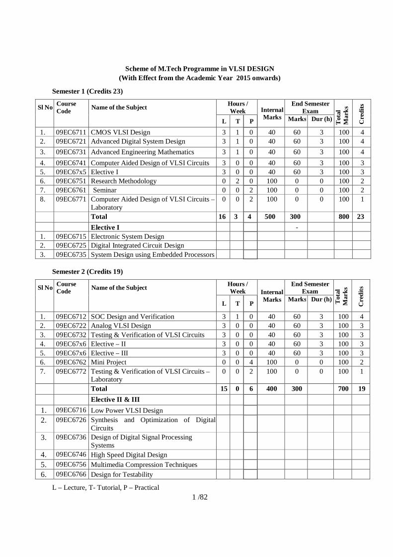
Scheme of M.Tech Programme in VLSI DESIGN (With Effect from the Academic Year 2015 onwards)
Semester 1 (Credits 23)
Sl No Course Code Name of the Subject Hours /
Week Internal Marks
End Semester Exam
Tot
al
Mar
ks
Cre
dits
L T P Marks Dur (h)
1. 09EC6711 CMOS VLSI Design 3 1 0 40 60 3 100 4 2. 09EC6721 Advanced Digital System Design 3 1 0 40 60 3 100 4 3. 09EC6731 Advanced Engineering Mathematics 3 1 0 40 60 3 100 4 4. 09EC6741 Computer Aided Design of VLSI Circuits 3 0 0 40 60 3 100 3 5. 09EC67x5 Elective I 3 0 0 40 60 3 100 3 6. 09EC6751 Research Methodology 0 2 0 100 0 0 100 2 7. 09EC6761 Seminar 0 0 2 100 0 0 100 2 8. 09EC6771 Computer Aided Design of VLSI Circuits –
Laboratory 0 0 2 100 0 0 100 1
Total 16 3 4 500 300 800 23 Elective I -
1. 09EC6715 Electronic System Design 2. 09EC6725 Digital Integrated Circuit Design 3. 09EC6735 System Design using Embedded Processors
Semester 2 (Credits 19)
Sl No Course Code Name of the Subject Hours /
Week Internal Marks
End Semester Exam
Tot
al
Mar
ks
Cre
dits
L T P Marks Dur (h)
1. 09EC6712 SOC Design and Verification 3 1 0 40 60 3 100 4 2. 09EC6722 Analog VLSI Design 3 0 0 40 60 3 100 3 3. 09EC6732 Testing & Verification of VLSI Circuits 3 0 0 40 60 3 100 3 4. 09EC67x6 Elective – II 3 0 0 40 60 3 100 3 5. 09EC67x6 Elective – III 3 0 0 40 60 3 100 3 6. 09EC6762 Mini Project 0 0 4 100 0 0 100 2 7. 09EC6772 Testing & Verification of VLSI Circuits –
Laboratory 0 0 2 100 0 0 100 1
Total 15 0 6 400 300 700 19 Elective II & III
1. 09EC6716 Low Power VLSI Design 2. 09EC6726 Synthesis and Optimization of Digital
Circuits
3. 09EC6736 Design of Digital Signal Processing Systems
4. 09EC6746 High Speed Digital Design 5. 09EC6756 Multimedia Compression Techniques 6. 09EC6766 Design for Testability
L – Lecture, T- Tutorial, P – Practical

2 /82
Semester 3 (Credits 14)
Sl No
Course Code Name of the Subject Hours /
Week Internal
Marks
End Semester Exam
Tot
al
Mar
ks
Cre
dits
L T P Marks
Dur (h)
1. 09EC77x7 Elective IV 3 0 0 40 60 3 100 3
2. 09EC77x7 Elective V 3 0 0 40 60 3 100 3
3. 09EC7763 Seminar 0 0 2 100 0 0 100 2
4. 09EC7783 Master Research Project Phase I 0 0 12
Gui
de
EC
0 0 6
20 30 50
Total 6 0 14 230 120 350 14
Elective IV & V
1. 09EC7717 Mixed Signal System Design 2. 09EC7727 FPGA Architecture & Applications 3. 09EC7737 Wireless Technologies 4. 09EC7747 System Verilog 5. 09EC7757 Hardware-Software Co-design 6. 09EC7767 VLSI Signal Processing
Semester 4 (Credits 12)
Sl No
Course Code Name of the Subject Hours /
Week Internal Marks
End Semester Exam
Tot
al
Mar
ks
Cre
dits
L T P Mark
s Dur (h)
1. 09EC7784 Master Research Project Phase II 0 0 21
Gui
de
Ext e
xper
t
EC
0 0 12
30 30 40 100
Total 0 0 21 100 0 100 12
Grand Total 1350 600 1950 68
EC-Evaluation Committee, L – Lecture, T- Tutorial, P – Practical, Teaching assistance of 6 hours/week
in all semesters for GATE students

3 /82
Examination Pattern
1. Theory Subjects
The examination pattern for all theory subjects is as given below.
Internal Continuous Assessment: 50 marks
Internal continuous assessment is in the form of periodical tests, assignments, seminars or a combination of all whichever suits best. There will be two tests per subject. The assessment details are to be announced to the students, right at the beginning of the semester by the teacher.
End Semester Examination: 50 marks
Question Pattern
Answer any 5 questions by choosing at least one question from each module.
Module 1 Module 2 Module 3 Module 4
Question 1 : 10 marks
Question 2 : 10 marks
Question 3 : 10 marks
Question 4 : 10 marks
Question 5 : 10 marks
Question 6 : 10 marks
Question 7 : 10 marks
Question 8 : 10 marks
2. Laboratory Subjects
The details of the internal assessment for each laboratory subject are as given below.
Mid Term Internal Test 40 Marks
Laboratory Experiments & Viva Voce 10 Marks
Final Internal Test 50 Marks
Total 100 Marks
3. Seminar/ Mini Projects
Seminar shall be evaluated by the evaluation committee based on the relevance of topic, content depth and breadth, communication skill, question answering etc on the power point presentation of the topic by the student.
Mini Projects shall be evaluated by the evaluation committee based on the demonstration of the project as well as power point presentation of the same.

4 /82
FIRST SEMESTER
Course No: 09EC6711
Course Title: CMOS VLSI DESIGN
Credits: 3-1-0: 4 Year : 2015
Pre-requisites: Nil
Objective:
To introduce students to basic concepts of digital VLSI chip design using the simpler
VLSI technology.
Have an understanding of the characteristics of CMOS circuit construction.
Be able to create models of moderately sized CMOS circuits that realize specified
digital functions.
Be able to design static CMOS combinational and sequential logic at the transistor
level, including mask layout
Have an understanding of CMOS Subsystem design, including data path and control
path.
Syllabus:
INTRODUCTION TO CMOS CIRCUITS,MOS Transistors, MOS Transistor Switches,
CMOS Logic, Circuit and System Representations, CMOS CIRCUIT AND LOGIC DESIGN
CMOS Logic Gate Design, Basic Physical Design of Simple Gate, CMOS Logic Structures,
Clocking Strategies, SYSTEMS DESIGN AND DESIGN METHOD, Design Strategies CMOS
Chip Design Options, CMOS SUB SYSTEM DESIGN,Data Path Operations-
Addition/Subtraction
Course Outcome:
After successful completion of the course, students should be able to:
Be able to create models of moderately sized CMOS circuits that realize specified
digital functions.

5 /82
Be able to apply CMOS technology-specific layout rules in the placement and routing
of transistors and interconnect, and to verify the functionality, timing, power, and
parasitic effects.
Have an understanding of the characteristics of CMOS circuit construction and the
comparison between different state-of-the-art CMOS technologies and processes.
Be able to complete a significant VLSI subsystem design project having a set of
objective criteria and design constraints.
TEXT BOOKS: 1. Neil. H.E. Weste and K. Eshragian, “Principles of CMOS VLSI Design”. 2nd Edition.
Addison-Wesley , 2000.
REFERENCES: 1. Douglas a. Pucknell and K. Eshragian., “Basic VLSI Design” 3rd Edition. PHI, 2000. 2. R. Jacob Baker, Harry W. LI., & David K. Boyce., “CMOS Circuit Design”, 3rd Indian
reprint, PHI, 2000.
3. Semiconductor Devices Modelling and Technology Nandita Das Guptha , Amitava Das Guptha; Prentice Hall India
4. Operation and Modeling of The MOS transistor : Yannis Tsividis 2/e Oxford
University Press 5. Kang & Leblebigi “CMOS Digital IC Circuit Analysis & Design”- McGraw Hill, 2003
6. Weste and Eshraghian, “Principles of CMOS VLSI design” Addison-Wesley, 2002 In addition, manufacturers Device data sheets and application notes are to be referred to get practical and application oriented information. Internal continuous assessment: 40 marks Internal continuous assessment : Test 1- 15 marks Test 2- 15 marks Assignment/Tutorial-10 marks Total-40marks COURSE PLAN: Course No: 09EC6711 Title: CMOS VLSI DESIGN (L-T-P): 3-1-0 Credits: 4
Modules Hours % marks in

6 /82
ESE Module 1 INTRODUCTION TO CMOS CIRCUITS MOS Transistors, MOS Transistor Switches, CMOS Logic, Circuit and
System Representations, MOS Transistor Theory - Introduction MOS Device
Design Equations, The Complementary CMOS Inverter-DC Characteristics,
Static Load MOS Inverters, The Differential Inverter, The Transmission Gate,
The Tri State Inverter, Bipolar Devices, Resistance Estimation Capacitance
Estimation, Inductance, Switching Characteristics CMOS-Gate Transistor
Sizing, Power Dissipation, Sizing Routing Conductors, Charge Sharing,
Design Margining, Reliability.
10 25
Module 2
CMOS CIRCUIT AND LOGIC DESIGN
CMOS Logic Gate Design, Basic Physical Design of Simple Gate, CMOS
Logic Structures, Clocking Strategies, I/O Structures, Low Power Design
9 25
FIRST INTERNAL TEST Module 3 SYSTEMS DESIGN AND DESIGN METHOD
Design Strategies CMOS Chip Design Options, Design Methods, Design
Capture Tools, Design Verification Tools, Design Economics, Data Sheets,
CMOS Testing - Manufacturing Test Principles, Design Strategies for Test,
Chip Level Test Techniques, System Level Test Techniques, Layout Design
for Improved Testability.
13 25
SECOND INTERNAL TEST Module 4 CMOS SUB SYSTEM DESIGN
Data Path Operations-Addition/Subtraction, Parity Generators, Comparators,
Zero/One Detectors, Binary Counters, ALUs, Multiplication, Shifters,
Memory Elements, Control-FSM, Control Logic Implementation.
10 25
Tutorial 14 END SEMESTER EXAMINATION
Total Hours 56

7 /82
Course No: 09EC6721
Course Title: ADVANCED DIGITAL SYSTEM DESIGN
Credits: 3-1-0: 4 Year : 2015
Pre-requisites: Nil
Objective: To prepare students for the design of practical digital hardware systems using VHDL. This course covers the basics of digital logic circuits and design and introduces the student to the fundamentals of combination logic design and then to sequential circuits (both synchronous and asynchronous). Memory systems are also covered. Students will be provided opportunities to synthesize the designs (using both schematic capture and VHDL) for implementation in FPGAs. Syllabus: Introduction to Digital Design, Combinational and Sequential Circuit Design, State machine design, Design of Asynchronous Sequential Circuit, Designing with PLDs, and CPLDs. HDL, Introduction to Synthesis and Synthesis Issues
Testing, Fault Modelling and Test Generation, Test generation for combinational logic circuits, Introduction to Design for Testability. FPGAs, Logic blocks, Routing architecture, Design flow technology, Xilinx and Altera FPGA Architecture. Course Outcome:
The students will be able to design, simulate, built and debug complex combinational and sequential circuits based on an abstract functional specification and implement the designs on FPGAs. TEXT BOOKS:
1. Parag K. Lala, "Digital System Design using programmable Logic Devices", Prentice Hall, NJ, 1994
2. Geoff Bestock, "FPGAs and programmable LSI; A Designers Handbook", Butterworth Heinemann, 1996
REFERENCES:
1. Miron Abramovici, Melvin A. Breuer and Arthur D. Friedman, “Digital Systems Testing and Testable Design”, John Wiley & Sons Inc.

8 /82
2. Parag K.Lala “Fault Tolerant and Fault Testable Hardware Design” B S Publications, 2002
3. J. Bhasker, "A VHDL Primer", Addison-Weseley Longman Singapore Pte Ltd. 1992 4. Jesse H. Jenkins, "Designing with FPGAs and CPLDs", Prentice Hall, NJ,1994 5. Fundamentals of Logic Design – Charles H. Roth, 5th ed., Cengage Learning. 6. Kevin Skahill, "VHDL for Programmable Logic", Addison -Wesley, 1996 7. Z. Navabi, "VHDL Analysis and Modeling of Digital Systems", McGRAW-Hill, 1998 8. Digital Circuits and Logic Design – Samuel C. Lee , PHI 9. Smith, "Application Specific Integrated Circuits", Addison-Wesley, 1997 10. P.K. Lala, “Digital Circuit Testing and Testability”, Academic Press, 2002
In addition, manufacturers Device data sheets and application notes are to be referred to get practical and application oriented information. Internal continuous assessment: 40 marks Internal continuous assessment : Test 1- 15 marks Test 2- 15 marks Assignment/Tutorial-10 marks Total-40marks COURSE PLAN: Course No: 09EC6721 Title: ADVANCED DIGITAL SYSTEM DESIGN (L-T-P): 3-1-0 Credits: 4
Modules Hours % marks in ESE
Module 1 Introduction to Digital Design Combinational Circuit Design, Synchronous Sequential Circuit Design - Mealy and Moore model, State machine design, Analysis of Synchronous sequential circuit, State equivalence, State Assignment and Reduction, Analysis of Asynchronous Sequential Circuit, flow table reduction, races, state assignment, Design of Asynchronous Sequential Circuit, Designing with PLDs – Overview of PLDs – ROMs, EPROMs – PLA – PAL - Gate Arrays – CPLDs and FPGAs, Designing with ROMs - Programmable Logic Arrays - Programmable Array logic, PAL series 16 & 22 – PAL22V10 - Design examples.
12 25
Module 2 VHDL Basics – Introduction to HDL – Behavioral modeling – Data flow modeling – Structural modeling – Basic language elements – Entity – Architecture – Configurations – Subprograms & operator overloading –
7 13

9 /82
Packages and libraries – Test Bench – Advanced Features – Model simulation FIRST INTERNAL TEST
Realization of combinational and sequential circuits using HDL – Registers – Flip flops – counters – Shift registers –Multiplexers – sequential machine –Multiplier – Divider, Introduction to Synthesis and Synthesis Issues.
5 12
Module 3 Testing, Fault Modelling And Test Generation – Introduction to testing – Faults in Digital Circuits – Modelling of faults – Logical Fault Models – Fault detection – Fault Location – Fault dominance – Logic simulation – Test generation for combinational logic circuits – Testable combinational logic circuit design, Introduction to Design for Testability, BST
8 25
SECOND INTERNAL TEST Module 4 FPGA - FPGAs - Logic blocks, Routing architecture, Design flow technology - mapping for FPGAs, Xilinx FPGA Architecture, Xilinx XC4000 - ALTERA’s FLEX 8000, Design flow for FPGA Design, Case studies: Virtex II Pro.
10 25
Tutorial 14 END SEMESTER EXAMINATION
Total Hours 56

10 /82
Course No: 09EC6731
Course Title: ADVANCED ENGINEERING MATHEMATICS
Credits: 3-1-0: 4 Year : 2015
Pre-requisites: Nil
Objective:
To understand methods of advanced engineering mathematics including advanced
methods found in solving linear ordinary differential equations, matrix inversion,
matrix factorization and vector spaces.
To understand basic concept of Orthogonality, Orthogonal bases and linear transforms.
To demonstrate knowledge of Laplace, Fourier and ‘Z’ transform methods in the
solution of a spectrum of applications in engineering.
To understand the importance of orthogonal and unitary transforms for various
engineering applications.
Demonstrate the application of unitary transforms for signal and image processing
applications.
To understand the basic concept of Wavelets and Wavelet Transform.
Syllabus: Linear Algebra, Linear Equations and Matrix Algebra, Linear Transforms, Orthogonality,
Digital Transforms and Arithmetic, 2D orthogonal & unitary transforms, Properties of unitary
transforms, 1D and 2D- DFT, Walsh, Hadamard Transform, Haar Transform, SVD Transform,
Digital Arithmetic, Wavelet Transform
Course Outcome:
After successful completion of the course, students should be able to get:
A sound understanding of system of linear equations and ability solve them.
A sound understanding of the Gauss elimination and ability to use it to solve linear
system.
A sound understanding of Matrix factorization, inversion and ability to solve them.
Ability to employ Laplace and Z transform to solve linear systems.

11 /82
A sound understanding of Orthogonality, Orthogonal bases and linear transforms.
Ability to employ linear transforms for solving signal and image processing
applications.
A sound understanding of Wavelets and Wavelet transform.
TEXT BOOKS: 1. “Linear Algebra and its Applications”, David C. Lay, 3rd edition, Pearson Education (Asia)
Pte. Ltd, 2005 2. Digital Arithmetic, Milos D. Ercegovac, Tomas Lang, Elsevier REFERENCES: 1. “Fundamentals of Digital Image Processing”, Anil K. Jain, PHI, New Delhi 2. Digital Signal Processing: a practical approach, Emmanuel C Ifeachor, W Barrie Jervis,
Pearson Education (Singapore) Pte. Ltd., Delhi 3. Wavelet transforms-Introduction to theory and applications, Raghuveer M.Rao and Ajit S.
Bapardikar, Person Education 4. Linear Algebra and its Applications, GilbertStrang. 5. Schaum's Outline for Advanced Engineering Mathematics for Engineers and Scientists ,
Murray R. Spiegel, MGH Book Co., New York 6. Advanced Engineering Mathematics, Erwin Kreyszing, John Wiley & Sons, NEW YORK 7. Advanced Engineering Mathematics, JAIN, R K,IYENGAR, S R K, Narosa, NEW YORK 8. Signal processing with fractals: a Wavelet - based approach, Wornell, Gregory, PH, PTR,
NEW JERSEY 5. Wavelet a primer, Christian Blatter, Universities press (India) limited, Hyderabad
Internal continuous assessment: 40 marks Internal continuous assessment : Test 1- 15 marks Test 2- 15 marks Assignment/Tutorial-10 marks Total-40marks COURSE PLAN:
Course No: 09EC6731 Title: ADVANCED ENGINEERING MATHEMATICS (L-T-P): 3-1-0 Credits: 4
Modules Hours % marks in ESE

12 /82
Module 1 : Linear Algebra Linear Equations and Matrix Algebra: Fields; system of linear equations, and its solution sets; elementary row operations and echelon forms; matrix operations; invertible matrices, LU-factorization Vector Spaces: Vector spaces; subspaces; bases ; dimension; coordinates
10 25
Module 2 : Linear Transforms Orthogonality: Orthogonal Vectors and Subspaces, Cosines and Projections onto lines, Projections and least squares, Orthogonal Bases and Gram-Schmidt orthogonalization.
6 13
FIRST INTERNAL TEST
Linear Systems and Shift invariance, The Laplace Transform, Properties, The Fourier Transform, Properties of Fourier Transform, Fourier Transform of Sequence(Fourier Series) and its properties, Z Transform and its properties.
7 12
Module 3: Digital Transforms and Arithmetic Introduction, 2D orthogonal & unitary transforms, Properties of unitary transforms, 1D and 2D- DFT, Walsh, Hadamard Transform, Haar Transform, SVD Transform. Digital Arithmetic: Fixed and Floating point representation, IEEE 754 Floating point standards, Floating point arithmetic operations.
10 25
SECOND INTERNAL TEST
Module 4: Wavelet Transform Wavelet Transform: Continuous: introduction, C-T wavelets, properties, inverse CWT. Discrete Harr Wavelet Transform and orthogonal wavelet decomposition using Harr Wavelets.
9 25
Tutorial 14
END SEMESTER EXAMINATION Total Hours 56

13 /82
Course No: 09EC6741
Course Title: COMPUTER AIDED DESIGN OF VLSI CIRCUITS
Credits: 3-0-0: 3 Year : 2015
Pre-requisites: Nil
Objective:
To provide an introduction to the fundamentals of Computer-Aided Design tools for the
modelling, design, analysis, test, and verification of digital Very Large Scale
Integration (VLSI) systems.
Have an understanding of VLSI Physical design and verification
Have an understanding of design for testability and testability measures for VLSI
circuits.
Syllabus: Various CAD Tools for front end and Back end design, Schematic editors, Layout editors,
Introduction to Design Tools: Introduction & Familiarity with Design Tools from various
vendors e.g. Synopsis, Mentor Tools etc. , Layout Algorithms Circuit partitioning, placement,
and routing algorithms; Design rule verification; Circuit Compaction;, , Automatic Test
Program Generation; Combinational testing D-Algorithm and PODEM algorithm; Scan-based
testing of sequential circuits; Testability measures for circuits.
Course Outcome:
After successful completion of the course, students should be able to:
Establish comprehensive understanding of the various phases of CAD for digital
electronic systems, from digital logic simulation to physical design, including test and
verification.
Demonstrate knowledge and understanding of fundamental concepts in CAD and to
establish capability for CAD tool development and enhancement.
TEXT BOOKS: 1. N.A. Sherwani, " Algorithms for VLSI Physical Design Automation ", 1999.

14 /82
REFERENCES: 1. S.H. Gerez, " Algorithms for VLSI Design Automation ", 1998.4. J. Bhasker, "A VHDL Primer",
Addison-Weseley Longman Singapore Pte Ltd. 1992
2. Drechsler, R., Evolutionary Algorithms for VLSI CAD, Kluwer Academic Publishers, Boston, 1998.
3. Verilog HDL by Samir Palnitkar 4. VERILOG HDL SYNTHESIS: A PRACTICAL PRIMER by J Bhaskar
5. Hill, D., D. Shugard, J. Fishburn and K. Keutzer, Algorithms and Techniques for VLSI Layout Synthesis, Kluwer Academic Publishers, Boston, 1989.
In addition, manufacturers Device data sheets and application notes are to be referred to get practical and application oriented information. Internal continuous assessment: 40 marks Internal continuous assessment : Test 1- 15 marks Test 2- 15 marks Assignment/Tutorial-10 marks Total-40marks COURSE PLAN: Course No: 09EC6741 Title: COMPUTER AIDED DESIGN OF VLSI CIRCUITS (L-T-P): 3-1-0 Credits: 4
Modules Hours % marks in ESE
Module 1 Various CAD Tools for front end and Back end design, Schematic editors,
Layout editors, Place and Route tools. Introduction to VLSI Methodologies -
VLSI Physical Design Automation - Design and Fabrication of VLSI Devices
- Fabrication process
10 25
Module 2 Introduction to Design Tools: Introduction & Familiarity with Design Tools
from various vendors e.g. Synopsis, Mentor Tools etc.
Verilog Basics - Modeling Levels - Data Types - Modules and Ports - Instances
- Basic Language Concepts - Dataflow modeling - Behavioral modeling
7 13
FIRST INTERNAL TEST

15 /82
Modeling and Simulation of systems/subsystems using Verilog HDL.
Typical case studies.
6 12
Module 3
Layout Algorithms Circuit partitioning, placement, and routing algorithms;
Design rule verification; Circuit Compaction; Circuit extraction and post-layout
simulation
10 25
SECOND INTERNAL TEST
Module 4
Automatic Test Program Generation; Combinational testing D-Algorithm and
PODEM algorithm; Scan-based testing of sequential circuits; Testability
measures for circuits.
9 25
END SEMESTER EXAMINATION Total Hours 56

16 /82
09EC6715 - ELECTIVE I
Course No: 09EC6715
Course Title: ELECTRONIC SYSTEM DESIGN
Credits: 3-0-0: 3 Year : 2015
Pre-requisites: Nil
Objective: To give the student a foundation in
practical analog, digital and mixed signal circuit design issues and techniques electromagnetic compatibility design issues packaging and thermal aspects in enclosure design
Syllabus:
Practical Analog & Mixed Signal Circuit Design Issues and Techniques, Op amps, ADCs and
DACs, Power supplies, Practical Logic Circuit Design Issues and Techniques, Design for
testability, Electromagnetic Compatibility (EMC), Cabling of Electronic Systems, Grounding
of Electronic Systems, Balancing & Filtering in Electronic Systems, Protection Against
Electrostatic Discharges (ESD), Packaging & Enclosures of Electronic System, Cooling in/of
Electronic System.
Course Outcome: After successful completion of the course, the student will have demonstrated an ability to
apply the practical design concepts in analog, digital and mixed signal circuits; design concepts
of EMC and ESD in PCB and system design; the design concepts of packaging and enclosure
design to take care of environmental and thermal requirements.
TEXT BOOKS:
1. Electronic Instrument Design, 1st edition; by: Kim R.Fowler; Oxford University Press. 2. Noise Reduction Techniques in Electronic Systems, 2nd edition; by: Henry W.Ott; John
Wiley & Sons. 3. Digital Design Principles& Practices, 3rd edition by: John F. Wakerly; Prentice Hall
International, Inc.

17 /82
REFERENCES: 1. Operational Amplifiers and linear integrated circuits, 3rd edition by: Robert F.
Coughlin; Prentice Hall International, Inc 2. Intuitive Analog circuit design by: Mark.T Thompson; Published by Elsevier 3. Printed Circuit Boards - Design & Technology, 1st edition; by: W Bosshart; Tata
McGraw Hill. 4. A Designer’s Guide to Instrumentation Amplifiers; by: Charles Kitchin and Lew
Counts; Seminar Materials @ http://www.analog.com 5. Errors and Error Budget Analysis in Instrumentation Amplifier Applications; by:
Eamon Nash; Application note AN-539@ http://www.analog.com 6. Practical Analog Design Techniques; by: Adolofo Garcia and Wes Freeman;
Seminar Materials@ http://www.analog.com 7. Selecting An A/D Converter; by:Larry Gaddy; Application bulletin @
http://www.Ti.com 8. Benefits and issues on migration of 5-volt and 3.3 volt logic to lower voltage
supplies; Application note SDAA011A@ http://www.Ti.com 9. JTAG/IEEE 1149.1 deigns considerations; Application note SCTA029@
http://www.Ti.com 10. Live Insertion; Application note SDYA012@ http://www.Ti.com 11. PCB Design Guidelines For Reduced EMI; Application note SZZA009@
http://www.Ti.com In addition, manufacturers Device data sheets and application notes are to be referred to get practical and application oriented information. Internal continuous assessment: 40 marks Internal continuous assessment : Test 1- 15 marks Test 2- 15 marks Assignment/Tutorial-10 marks Total-40marks COURSE PLAN: Course No: 09EC6715 Title: ELECTRONIC SYSTEM DESIGN (L-T-P): 3-0-0 Credits: 3
Modules Hours % marks in ESE
Module 1 Practical Analog & Mixed Signal Circuit Design Issues and Techniques: Passive components: Understanding and interpreting data sheets and specifications of various passive and active components, non-ideal behavior of passive components,.
10 25

18 /82
Op amps: DC performance of op amps: Bias, offset and drift. AC Performance of operational amplifiers: band width, slew rate and noise. Properties of a high quality instrumentation amplifier. Design issues affecting dc accuracy & error budget analysis in instrumentation amplifier applications. Isolation amplifier basics. Active filers: design of low pass, high pass and band pass filters.
ADCs and DACs: Characteristics, interfacing to microcontrollers. Selecting an ADC.
Power supplies: Characteristics, design of full wave bridge regulated power supply. Circuit layout and grounding in mixed signal system.
Module 2 Practical Logic Circuit Design Issues and Techniques:
Understanding and interpreting data sheets & specifications of various CMOS& BiCMOS family Logic devices. Electrical behavior (steady state & dynamic) of CMOS& BiCMOS family logic devices.
6 13
FIRST INTERNAL TEST Benefits and issues on migration of 5-volt and 3.3 volt logic to lower voltage supplies. CMOS/TTL Interfacing Basic design considerations for live insertion. JTAG/IEEE 1149.1 design considerations.
Design for testability, Estimating digital system reliability. Digital circuit layout and grounding. PCB design guidelines for reduced EMI.
6 12
Module 3 Electromagnetic Compatibility (EMC): Designing for (EMC), EMC regulations, typical noise path, methods of noise coupling, methods of reducing interference in electronic systems. Cabling of Electronic Systems:
Capacitive coupling, effect of shield on capacitive coupling, inductive coupling, effect of shield on inductive coupling, effect of shield on magnetic coupling, magnetic coupling between shield and inner conductor, shielding to prevent magnetic radiation, shielding a receptor against magnetic fields, coaxial cable versus shielded twisted pair, ribbon cables. Grounding of Electronic Systems: Safety grounds, signal grounds, single-point
10 25
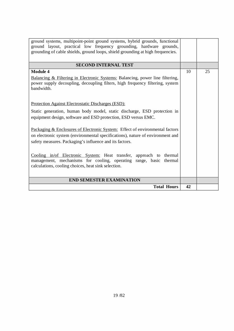
19 /82
ground systems, multipoint-point ground systems, hybrid grounds, functional ground layout, practical low frequency grounding, hardware grounds, grounding of cable shields, ground loops, shield grounding at high frequencies.
SECOND INTERNAL TEST Module 4 Balancing & Filtering in Electronic Systems: Balancing, power line filtering, power supply decoupling, decoupling filters, high frequency filtering, system bandwidth.
Protection Against Electrostatic Discharges (ESD): Static generation, human body model, static discharge, ESD protection in equipment design, software and ESD protection, ESD versus EMC. Packaging & Enclosures of Electronic System: Effect of environmental factors on electronic system (environmental specifications), nature of environment and safety measures. Packaging’s influence and its factors.
Cooling in/of Electronic System: Heat transfer, approach to thermal management, mechanisms for cooling, operating range, basic thermal calculations, cooling choices, heat sink selection.
10 25
END SEMESTER EXAMINATION Total Hours 42

20 /82
09EC6725 - ELECTIVE I
Course No: 09EC6725
Course Title: DIGITAL INTEGRATED CIRCUIT DESIGN
Credits: 3-0-0: 3 Year : 2015
Pre-requisites: Nil
Objective:
To introduce the fundamental principles of VLSI circuit design and to examine the
basic building blocks of large-scale digital integrated circuits.
Have an understanding of CMOS inverter characteristics and transistor sizing.
To introduce CMOS design of Arithmetic building blocks and Memories.
To understand the importance of BiCMOS technology.
Syllabus:
CMOS inverters -static and dynamic characteristics, CMOS NAND, NOR and XOR Gates
Static and Dynamic CMOS design- Domino and NORA logic - combinational and sequential
circuits -Method of Logical Effort for transistor sizing -power consumption in CMOS gates-
Low power CMOS design,Arithmetic circuits in CMOS VLSI - Adders- multipliers- shifter -
CMOS memory design - SRAM and DRAM , Bipolar gate Design- BiCMOS logic - static and
dynamic behaviour -Delay and power consumption in BiCMOS Logic.
Course Outcome:
After successful completion of the course, students should be able to:
Be able to understand CMOS inverter characteristics and transistor sizing for
performance and power optimization.
Able to design CMOS complex circuits like Multipliers, shifters, memories etc.
Be able to understand the advantages of BiCMOS technology

21 /82
TEXT BOOKS: 1. Sung-Mo Kang & Yusuf Leblebici, CMOS Digital Integrated Circuits - Analysis & Design,
MGH, Second Ed., 1999
REFERENCES: 1. Jan M Rabaey, Digital Integrated Circuits - A Design Perspective, Prentice Hall, 1997
2. Ken Martin, Digital Integrated Circuit Design, Oxford University Press, 2000 3. R. J. Baker, H. W. Li, and D. E. Boyce, CMOS circuit design, layout, and simulation. New
York: IEEE Press, 1998. 4. Analysis and Design of Digital Integrated Circuits, Third Edition, David A. Hodges,
Horace G. Jackson, and Resve A. Saleh, McGraw-Hill, 2004. In addition, manufacturers Device data sheets and application notes are to be referred to get practical and application oriented information. Internal continuous assessment: 40 marks Internal continuous assessment : Test 1- 15 marks Test 2- 15 marks Assignment/Tutorial-10 marks Total-40marks COURSE PLAN: Course No: 09EC6725 Title: DIGITAL INTEGRATED CIRCUIT DESIGN (L-T-P): 3-0-0 Credits: 3
Modules Hours % marks in ESE
Module 1
CMOS inverters -static and dynamic characteristics, CMOS NAND, NOR and
XOR Gates
10 25
Module 2
Static and Dynamic CMOS design- Domino and NORA logic - combinational
and sequential circuits -Method of Logical Effort for transistor sizing -power
consumption in CMOS gates- Low power CMOS design
13 25
FIRST INTERNAL TEST

22 /82
Module 3
Bipolar gate Design- BiCMOS logic - static and dynamic behaviour -Delay and
power consumption in BiCMOS Logic.
10 25
SECOND INTERNAL TEST
Module 4
Arithmetic circuits in CMOS VLSI - Adders- multipliers- shifter -CMOS
memory design - SRAM and DRAM
9 25
END SEMESTER EXAMINATION Total Hours 42

23 /82
09EC6735 - ELECTIVE I
Course No: 09EC6735
Course Title: SYSTEM DESIGN USING EMBEDDED PROCESSORS
Credits: 3-0-0: 3 Year : 2015
Pre-requisites: Nil
Objective: The objective is to impart the concepts and architecture of Embedded systems and to make the students capable of designing Embedded systems. To achieve this, the architecture and programming of Industry popular 32-bit Microcontroller, ARM Cortex is covered in detail. Syllabus: Embedded Concepts, Architecture of embedded systems, ARM Architecture, Cortex-M3 Basics, Exceptions, Instruction Sets, NVIC, Interrupt Behaviour, Cortex-M3/M4 Programming, Exception Programming, Memory Protection Unit and other Cortex-M3 features, STM32L15xxx ARM Cortex M3/M4 Microcontroller Memory and Peripherals, Development & Debugging Tools. Course Outcome: After successful completion of the course, students should be able to:
Understand the Embedded Concepts and Architecture of Embedded Systems Understand the architecture and programming of Industry standard 32-bit popular ARM Cortex Microcontroller Select a proper Microcontroller for a particular application Understand the usage of the development and debugging tools.
TEXT BOOKS:
1. The Definitive Guide to the ARM Cortex-M3, Joseph Yiu, Second Edition, Elsevier Inc. 2010.
2. Andrew N Sloss, Dominic Symes, Chris Wright, “ARM System Developer's Guide - Designing and Optimizing System Software”, 2006, Elsevier.
REFERENCES: 1. Steve Furber, “ARM System-on-Chip Architecture”, 2nd Edition, Pearson Education 2. Cortex-M series-ARM Reference Manual 3. Cortex-M3 Technical Reference Manual (TRM) 4. Embedded/Real Time Systems Concepts, Design and Programming Black Book,
Prasad, KVK.

24 /82
5. David Seal “ARM Architecture Reference Manual”, 2001 Addison Wesley, England; Morgan Kaufmann Publishers
6. STM32L152xx ARM Cortex M3 Microcontroller Reference Manual 7. ARM Company Ltd. “ARM Architecture Reference Manual– ARM DDI 0100E” 8. ARM v7-M Architecture Reference Manual (ARM v7-M ARM). 9. Ajay Deshmukh, “Microcontroller - Theory & Applications”, Tata McGraw Hill 10. Arnold. S. Berger, “Embedded Systems Design - An introduction to Processes,
Tools and Techniques”, Easwer Press 11. Raj Kamal, “Microcontroller - Architecture Programming Interfacing and System
Design” 1st Edition, Pearson Education In addition, manufacturers Device data sheets and application notes are to be referred to get practical and application oriented information. Internal continuous assessment: 40 marks Internal continuous assessment : Test 1- 15 marks Test 2- 15 marks Assignment/Tutorial-10 marks Total-40marks COURSE PLAN: Course No: 09EC6735 Title: SYSTEM DESIGN USING EMBEDDED PROCESSORS (L-T-P): 3-0-0 Credits: 3
Modules Hours % marks in ESE
Module 1
Embedded Concepts Introduction to embedded systems, Application Areas, Categories of embedded systems, Overview of embedded system architecture, Specialties of embedded systems, recent trends in embedded systems, Architecture of embedded systems, Hardware architecture, Software architecture, Application Software, Communication Software, Development and debugging Tools.
ARM Architecture Background of ARM Architecture, Architecture Versions, Processor Naming, Instruction Set Development, Thumb-2 and Instruction Set Architecture.
10 25
Module 2 Overview of Cortex-M3 Cortex-M3 Basics: Registers, General Purpose Registers, Stack Pointer, Link
7 13

25 /82
Register, Program Counter, Special Registers, Operation Mode, Exceptions and Interrupts, Vector Tables, Stack Memory Operations, Reset Sequence. Instruction Sets: Assembly Basics, Instruction List, Instruction Descriptions. Cortex-M3 Implementation Overview: Pipeline, Block Diagram, Bus Interfaces on Cortex-M3, I-Code Bus, D-Code Bus, System Bus, External PPB and DAP Bus.
FIRST INTERNAL TEST Exceptions: Exception Types, Priority, Vector Tables, Interrupt Inputs and Pending Behavior, Fault Exceptions, Supervisor Call and Pendable Service Call. NVIC: Nested Vectored Interrupt Controller Overview, Basic Interrupt Configuration, Software Interrupts and SYSTICK Timer. Interrupt Behavior: Interrupt/Exception Sequences, Exception Exits, Nested Interrupts, Tail-Chaining Interrupts, Late Arrivals and Interrupt Latency
6 12
Module 3 Cortex-M3/M4 Programming: Cortex-M3/M4 Programming: Overview, Typical Development Flow, Using C, CMSIS (Cortex Microcontroller Software Interface Standard), Using Assembly. Exception Programming: Using Interrupts, Exception/Interrupt Handlers, Software Interrupts, Vector Table Relocation. Memory Protection Unit and other Cortex-M3 features: MPU Registers, Setting Up the MPU, Power Management, Multiprocessor Communication.
10 25
SECOND INTERNAL TEST Module 4 Cortex-M3/M4 Microcontroller STM32L15xxx ARM Cortex M3/M4 Microcontroller: Memory and Bus Architecture, Power Control, Reset and Clock Control. STM32L15xxx Peripherals: GPIOs, System Configuration Controller, NVIC, ADC, Comparators, GP Timers, USART. Development & Debugging Tools: Software and Hardware tools like Cross Assembler, Compiler, Debugger, Simulator, In-Circuit Emulator (ICE), Logic Analyzer etc.
9 25
END SEMESTER EXAMINATION Total Hours 42

26 /82
Course No: 09EC6751
Course Title: RESEARCH METHODOLOGY
Credits: 0-2-0: 2 Year : 2015
Pre-requisites: Nil
Objective:
To give students an insight into the steps to be followed in doing a research To provide an idea about technical report writing
Syllabus: Introduction to Research Methodology; Formulating a Research Problem; Conceptualising a research design; Methods of Data Collection; Processing and Analysis of Data; Writing a Research Report; Ethical issues related to publishing; A study of the use of the following tools like Matlab and LaTeX. Course Outcome: Students who successfully complete this course will have clear understanding about the steps to be followed in doing research. Text Books:
1. Ranjit Kumar, “Research Methodology: A Step-by-step Guide for Beginners”, Pearson, Second Edition
2. Kothari, C.R, “Research Methodology : Methods and Techniques”, New age International publishers
Reference Books: 1. Sanjit K. Mitra, “Digital Signal Processing Laboratory Using MATLAB” , Mcgraw-
Hill College, ISBN-13: 978-0073108582 2. Rudra Pratap, “Getting Started with MATLAB: Version 6: A Quick Introduction for
Scientists and Engineers”, 2001, Oxford University Press 3. Wayne Goddard and Stuart Melville, “Research Methodology : An Introduction”, 2nd
Edition, 2001, Juta & Co Ltd Internal continuous assessment: 100 marks Internal continuous assessment : Test 1- 30 marks Test 2- 30 marks Assignment/Tutorial-40 marks Total-100marks

27 /82
COURSE PLAN: Course No: 09EC6751 Title: RESEARCH METHODOLOGY (L-T-P): 0-2-0 Credits: 2
Modules Hours % marks in ESE
Module 1
Research Methodology: An Introduction Meaning of Research, Objectives of Research, Motivation in Research, Applications of Research, Definition of Research, Characteristics of Research, Types of Research, Steps in Research Process
Formulating a Research Problem Reviewing the Literature, Formulating a Research Problem, Identifying Variables, Constructing Hypothesis
7 25
Module 2 Conceptualising a research design
Definition of a Research Design, Need for Research Design, Functions of Research Design, Features of a Good Design
Methods of Data Collection Collection of Primary Data, Observation Method, Interview Method
Collection of Data through Questionnaires, Collection of Data through Schedules
7 25
FIRST INTERNAL TEST Module 3
Processing and Analysis of Data Processing Operations, Elements/Types of Analysis, Statistics in Research, Measures of Central Tendency, Measures of Dispersion, Measures of Asymmetry (Skewness)
Writing a Research Report Research writing in general, Referencing, Writing a Bibliography Developing an outline, Writing about a variable
7 25
Module 4 Interpretation of Data and Paper Writing – Layout of a Research Paper, Journals in Computer Science, Impact factor of Journals, When and where to publish?, Ethical issues related to publishing, Plagiarism and Self-Plagiarism.
A study of the use of the following tools - Matlab / Simulink, LaTeX/ MS
Office.
7 25
SECOND INTERNAL TEST Total Hours 28

28 /82
Course No: 09EC6761
Course Title: SEMINAR
Credits: 3-0-0: 3 Year : 2015
Pre-requisites: Nil
Objective: To assess the debating capability of the student to present a technical topic. Also to impart training to students to face audience and present their ideas and thus creating in them self esteem and courage that are essential for engineers. Syllabus: Individual students are required to choose a topic of their interest from VLSI related topics preferably from outside the M.Tech syllabus and give a seminar on that topic about 30 minutes. A committee consisting of at least three faculty members (preferably specialized in Embedded Systems) shall assess the presentation of the seminar and award marks to the students. Each student shall submit two copies of a write up of his/her seminar topic. One copy shall be returned to the student after duly certifying it by the chairman of the assessing committee and the other will be kept in the departmental library. Internal continuous assessment marks are awarded based on the relevance of the topic, presentation skill, quality of the report and participation. Course Outcome: After successful completion of the seminar, students should get exposed to new areas of technology and their communication, presentation skills etc. shall be improved. They shall be ready for technical paper writing and presentation. Internal continuous assessment: 100 marks Subject Relevance : 10 marks
Concept/ Knowledge in the topic : 20 marks
Presentation : 40 marks
Report : 30 marks
Total marks : 100 marks

29 /82
Course No: 09EC6771
Course Title: COMPUTER AIDED DESIGN OF VLSI CIRCUITS LABORATORY
Credits: 0-0-2: 1 Year : 2015
Pre-requisites: Nil
Objective:
The objective of this lab is to familiarize the students with the basics of VLSI CAD tool.
Learn how to manage files with the Library Manager, understand the basics of the
Schematics Editor, compile and simulation of combinational and sequential circuits.
Verilog modeling and simulation of complex digital circuits.
Small and Large signal MOSFET using C
Understanding of SPICE tool for CMOS Circuit simulation.
Syllabus: Familiarization of VLSI CAD tools, Verilog modeling and simulation of complex digital
circuits, MOSFET using C, SPICE tools for CMOS circuit simulation.
Course Outcome:
Students are able to use VLSI CAD Tool for verification of functionality and
simulation of RTL Verilog model.
Students will be able to understand MOS Small and Large signal models and generate
the characteristics curves.
Able to design CMOS circuits and model using SPICE Tool.
Text Books:
1. Modern Digital Electronics by R P Jain
Reference Books:
1. Verilog HDL by Samir Palnitkar.
2. VERILOG HDL SYNTHESIS: A PRACTICAL PRIMER by J Bhaskar

30 /82
Internal continuous assessment: 100 marks Internal continuous assessment : Test 1- 40 marks Test 2- 50 marks Laboratory Experiments & Viva Voce -10 marks Total-100marks COURSE PLAN: Course No: 09EC6771 Title: COMPUTER AIDED DESIGN OF VLSI CIRCUITS LABORATORY
(L-T-P): 0-0-2 Credits: 1 Modules Hours % marks
in ESE
Module 1 1. Modeling and simulation of Combinational and sequential circuits using
Verilog. 2. Modeling and Simulation of ALU using Verilog.
3. Modeling and Simulation of FSMs using Verilog 4. Modeling and simulation of Memory and FIFO in Verilog
12 40
FIRST INTERNAL TEST
Module 2 1. Modeling and simulation of UART in Verilog
2. Simulation of NMOS and CMOS circuits using SPICE. 3. Modeling of MOSFET using C.
14 60
SECOND INTERNAL TEST Total Hours 28
Internal Continuous Assessment: 100 marks
Internal continuous assessment is in the form of periodical tests. There will be a minimum of two tests per subject. The assessment details are to be announced to the students, right at the beginning of the semester by the teacher.
Mid Term Internal Test 40 Marks
Laboratory Experiments & Viva Voce 10 Marks
Final Internal Test 50 Marks
Total 100 Marks

31 /82
SECOND SEMESTER Course No: 09EC6712
Course Title: SOC DESIGN AND VERIFICATION
Credits: 3-1-0: 4 Year : 2015
Pre-requisites: Nil
Objective:
To understand the System on Chip with its need, evolution, challenges, goals,
superiority over system on board & stacked ICs in package.
To analyze how the SoCs are designed in industrial environment using different design
methodologies with the use of intellectual property, the challenges faced with IP
integration, design techniques to meet timing closure.
To understand the complexity of VLSI testing & verification, OOP based verification
and verification methodologies.
Discuss the importance of integrating memory components in the SoC and need,
selection criteria, types, principle of operation of different memory components (RAM
Cache memories with coherency protocols, Flash memories).
To understand problems in using traditional bus based communication architecture and
solve the problems imposed by bus based architecture using network on chip.
Syllabus:
System On Chip Design Process: A canonical SoC Design, SoC Design flow waterfall vs
spiral, topdown vs Bottom up, , Macro Design Process: Top level Macro Design, Macro
Integration, Soft Macro productization, Developing hard macros, Design issues for hard
macros, SoC Verification: Verification technology options, Verification methodology, Design
of Communication Architectures For SoCs: On chip communication architectures, System
level analysis for designing communication
Course Outcome:
After successful completion of the course, students should be able to:
Understanding of complexity in SoC Design.
Analyze the top-down and bottom-up design flows, timing problems on STA.

32 /82
Understanding of VLSI testing & verification,OOPs based verification and verification
methodologies .
Understanding of Communication based architectures for SoCs.
TEXT BOOKS: 1. “SoC Verification Methodology and Techniques”, Prakash Rashinkar Peter Paterson and
Leena Singh. Kluwer Academic Publishers, 2001.
REFERENCES: 1. “Reuse Methodology manual for SystemOnAChip Designs”, Michael Keating, Pierre
Bricaud, Kluwer Academic Publishers, second edition,2001.
2. “Design Verification: Simulation and Formal Method based Approaches”, William K. Lam, Prentice Hall.
3. “System- on -a- Chip Design and Test”, Rochit Rajsuman, ISBN.
4. “Multiprocessor Systemsonchips”, A.A. Jerraya, W.Wolf, M K Publishers.
5. “The EDA HandBook”, Dirk Jansen, Kluwer Academic Publishers.
In addition, manufacturers Device data sheets and application notes are to be referred to get practical and application oriented information. Internal continuous assessment: 40 marks Internal continuous assessment : Test 1- 15 marks Test 2- 15 marks Assignment/Tutorial-10 marks Total-40marks COURSE PLAN: Course No: 09EC6712 Title: SOC DESIGN AND VERIFICATION (L-T-P): 3-1-0 Credits: 4
Modules Hours % marks in ESE
Module 1
System On Chip Design Process: A canonical SoC Design, SoC Design flow
waterfall vs spiral, topdown vs Bottom up.
12 25

33 /82
Specification requirement, Types of Specification , System Design process,
System level design issues, Soft IP Vs Hard IP, Design for timing closure,Logic
design issues
Verification strategy, Onchip buses and interfaces, Low Power, Manufacturing
test strategies.
Module 2
Macro Design Process: Top level Macro Design, Macro Integration, Soft
Macro productization, Developing hard macros, Design issues for hard macros,
Design ,System Integration with reusable macros.
9 25
FIRST INTERNAL TEST
Module 3
SoC Verification: Verification technology options, Verification methodology,
Verification languages, Verification approaches, and Verification plans. System
level verification, Block level verification, Hardware/software co verification
and Static net list verification.
Verification architecture, Verification components, Introduction to VMM,
OVM and UVM.
10 25
SECOND INTERNAL TEST
Module 4
Design of Communication Architectures For SoCs:
On chip communication architectures, System level analysis for designing
communication, Design space exploration, Adaptive communication
architectures, Communication architecture tuners, Communication architectures
for energy/battery efficient systems.
Introduction to bus functional models and bus functional model based
verification.
11 25
Tutorial 14 END SEMESTER EXAMINATION
Total Hours 56

34 /82
Course No: 09EC6722
Course Title: ANALOG VLSI DESIGN
Credits: 3-0-0: 3 Year : 2015
Pre-requisites: Nil
Objective:
To introduces the principles of analog IC design in CMOS technologies.
To design and analysis fundamental building blocks and basic analog circuits, to
provide a foundation for more complicated and advanced designs.
To design and analysis of Differential Amplifiers, CMOS OPAMPS,PLL etc
To understand the basic principles of switched capacitor circuits and CMOS data
converters.
Syllabus: Analog MOS transistor models Temperature effects and Noise in MOS transistor MOS
resistors, characterization of resistive, capacitive elements and MOS devices. Passive and
active CMOS current sink/ sources– basics of single stage CMOS amplifiers common Source,
common gate and source follower stages frequency response.
CMOS Differential Amplifiers, High Performance Opamps – High speed/ high frequency
opamps,micro power opamps, low noise opamps and low voltage opamps. Current mirrors,
filter implementations.Supply independent and temperature independent references Band gap
references PTAT current generation and constant Gm biasing – CMOS comparators –
Multipliers and wave shaping circuits – effects due to nonlinearity and mismatch in MOS
circuits Switched Capacitor Circuits: Delay locked loops and applications, basics of CMOS
data converters – Medium and high speed CMOS data converters, Over sampling converters.
Course Outcome: After successful completion of the course, students should be able to:
Understanding of MOS transistor models for various active and passive components.
Analysis and design of CMOS Differential Amplifiers , OPAMPs and PLLs.

35 /82
Understanding the use of switched capacitor circuits and data converts in Analog IC
Design.
TEXT BOOKS:
1. “Analog Integrated Circuit Design”, David. A. Johns and Ken Martin, John Wiley and Sons, 2001.
REFERENCES: 1. “Design of Analog CMOS Integrated Circuit”, Behzad Razavi, Tata McGraw HILL,
2002. 2. “CMOS Analog Circuit Design”, Philip Allen & Douglas Holberg, Oxford University
Press, 2002. 3. “Analog VLSI – Signal Information and Processing”, Mohammed Ismail & Feiz , John Wiley
and Sons.
In addition, manufacturers Device data sheets and application notes are to be referred to get practical and application oriented information. Internal continuous assessment: 40 marks Internal continuous assessment : Test 1- 15 marks Test 2- 15 marks Assignment/Tutorial-10 marks Total-40marks COURSE PLAN: Course No: 09EC6722 Title: ANALOG VLSI DESIGN (L-T-P): 3-0-0 Credits: 3
Modules Hours % marks in ESE
Module 1
Analog MOS transistor models Temperature effects and Noise in MOS
transistor MOS resistors, characterization of resistive, capacitive elements and
MOS devices. Passive and active CMOS current sink/ sources– basics of single
stage CMOS amplifiers common Source, common gate and source follower
stages frequency response.
10 25

36 /82
Module 2
CMOS Differential Amplifiers: CMOS Operational Amplifiers one stage and
two stage gain boosting Common mode feedback (CMFB) Cascode and Folded
cascade structures
7 13
FIRST INTERNAL TEST
High Performance Opamps – High speed/ high frequency opamps,
micro power opamps, low noise opamps and low voltage opamps. Current
mirrors, filter implementations.
6 12
Module 3
Supply independent and temperature independent references Band gap
references PTAT current generation and constant Gm biasing – CMOS
comparators – Multipliers and wave shaping circuits – effects due to
nonlinearity and mismatch in MOS circuits
10 25
SECOND INTERNAL TEST
Module 4
Switched Capacitor Circuits: First and Second Order Switched Capacitor
Circuits, Switched Capacitor filters, CMOS oscillators, simple and charge
pump CMOS PLLs non ideal effects in PLLs, Delay locked loops and
applications, basics of CMOS data converters – Medium and high speed CMOS
data converters, Over sampling converters.
9 25
END SEMESTER EXAMINATION Total Hours 42

37 /82
Course No: 09EC6732
Course Title: TESTING & VERIFICATION OF VLSI CIRCUITS
Credits: 3-0-0: 3 Year : 2015
Pre-requisites: Nil
Objective:
To understand issues in test and verification of complex VLSI chips.
To know the various types of faults and also to study about fault detection and design
for testability.
To learn about SoC testing, test automation and BIST
To learn various design verification techniques and perform verification of simple IPs.
Syllabus:
Introduction: Scope of testing and verification in VLSI design process; Issues in test and verification of complex chips; embedded cores and SOCs
Introduction to test benches, writing test benches in Verilog HDL.
Fundamentals of VLSI testing, Fault models. Automatic test pattern generation, Design for testability, Scan design, Test interface and boundary scan.
System Testing and test for SOCs, Iddq testing, Delay fault testing, BIST for testing of logic and memories, Test automation.
Design Verification Techniques based on simulation, analytical and formal approaches, Functional verification, Timing verification, Formal verification, Basics of equivalence checking and model checking.
Verification of simple IPs: Memory verification, FIFO verification and Verification of RISC CPU
Course Outcome: After successful completion of the course, students should be able to:
Understand the issues in SoC Verification.
Get knowledge of various falts in digital circuits and design for testability.
Understand BIST and test automation for SoC verification.
Learn how to perform automated verification of IPs

38 /82
TEXT BOOKS:
1. M. Abramovici, M. A. Breuer, A. D. Friedman, “Digital Systems Testing and Testable Design” Piscataway, New Jersey: IEEE Press, 1994
REFERENCES: 1. M. Bushnell and V. D. Agarwal, "Essentials of Electronic Testing for Digital, Memory
and Mixed-Signal VLSI Circuits", Kluwer Academic Publishers, 2000 2. T.Kropf, "Introduction to Formal Hardware Verification", Springer Verlag, 2000. 3. P. Rashinkar, Paterson and L. Singh, "System-on-a-Chip Verification-Methodology and
Techniques", Kluwer Academic Publishers, 2001.
4. Samiha Mourad and Yervant Zorian, “Principles of Testing Electronic Systems”, Wiley (2000).
5. “SoC Verification Methodology and Techniques”, Prakash Rashinkar Peter Paterson
and Leena Singh .Kluwer Academic Publishers, 2001. 6. “Reuse Methodology manual for System On A Chip Designs”, Michael Keating, 7. Pierre Bricaud, Kluwer Academic Publishers, second edition, 2001. 8. “System- on -a- Chip Design and Test”, Rochit Rajsuman, ISBN.
In addition, manufacturers Device data sheets and application notes are to be referred to get practical and application oriented information. Internal continuous assessment: 40 marks Internal continuous assessment : Test 1- 15 marks Test 2- 15 marks Assignment/Tutorial-10 marks Total-40marks COURSE PLAN: Course No: 09EC6732 Title: TESTING & VERIFICATION OF VLSI CIRCUITS (L-T-P): 3-0-0 Credits: 3
Modules Hours % marks in ESE

39 /82
Module 1
Introduction: Scope of testing and verification in VLSI design process; Issues
in test and verification of complex chips; embedded cores and SOCs
Introduction to test benches, writing test benches in Verilog HDL.
10 25
Module 2
Fundamentals of VLSI testing, Fault models. Automatic test pattern
generation, Design for testability, Scan design, Test interface and boundary
scan.
10 25
FIRST INTERNAL TEST
Module 3
System Testing and test for SOCs, Iddq testing, Delay fault testing, BIST for
testing of logic and memories, Test automation.
10 25
SECOND INTERNAL TEST
Module 4
Design Verification Techniques based on simulation, analytical and formal
approaches, Functional verification, Timing verification, Formal verification,
Basics of equivalence checking and model checking.
Verification of simple IPs: Memory verification, FIFO verification and
Verification of RISC CPU
12 25
Tutorial 14 END SEMESTER EXAMINATION
Total Hours 56

40 /82
09EC67x6 - ELECTIVE II &
09EC67x6 - ELECTIVE III
Course No: 09EC6716
Course Title: LOW POWER VLSI DESIGN
Credits: 3-0-0: 3 Year : 2015
Pre-requisites: Nil
Objective:
To study the concepts on different levels of power estimation and optimization
techniques.
An exhaustive review of stateof-the-art techniques for power estimation and
optimization of digital VLSI systems.
To learn problems of modeling, estimation and optimization of power consumption at
different levels of abstraction.
Syllabus: Introduction - Simulation - Power Analysis-Probabilistic Power Analysis, Circuit -Logic - Special Techniques - Architecture and Systems, Advanced Techniques - Low Power CMOS VLSI Design - Physics of Power Dissipation in CMOS FET Devices, Power Estimation - Synthesis for Low Power - Design and Test of Low Voltages - CMOS Circuits. Low Power Static RAM Architectures -Low Energy Computing Using Energy Recovery Techniques – Software Design for Low Power.
Course Outcome: After successful completion of the course, students should be able to:
Identify the sources of power dissipation in digital IC systems.
Understand the impact of power on system performance and reliability.
Characterize and model power consumption, understand the basic analysis methods.
Understand the voltage scaling approaches for different design abstraction levels.
Apply probabilistic analysis to characterize dynamic power estimation.

41 /82
Understand leakage sources and reduction technique.
TEXT BOOKS:
1. Gary Yeap " Practical Low Power Digital VLSI Design ", 1997.
REFERENCES:
1. Kaushik Roy, Sharat Prasad, " Low Power CMOS VLSI Circuit Design ", 20003. 2. A.P.Chandrakasan and R.W. Broadersen, Low power digital CMOS design,
Kluwer,1995. 3. CMOS Analog Circuit Design”, Philip Allen & Douglas Holberg, Oxford University
Press, 2002. 4. Rabaey, Pedram, “Low power design methodologies” Kluwer Academic, 1997
In addition, manufacturers Device data sheets and application notes are to be referred to get practical and application oriented information. Internal continuous assessment: 40 marks Internal continuous assessment : Test 1- 15 marks Test 2- 15 marks Assignment/Tutorial-10 marks Total-40marks COURSE PLAN: Course No: 09EC6716 Title: LOW POWER VLSI DESIGN (L-T-P): 3-0-0 Credits: 3
Modules Hours % marks in ESE
Module 1
Introduction - Simulation - Power Analysis-Probabilistic Power Analysis.
10 25
Module 2
Circuit -Logic - Special Techniques - Architecture and Systems.
10 13
FIRST INTERNAL TEST

42 /82
Module 3
Advanced Techniques - Low Power CMOS VLSI Design - Physics of Power
Dissipation in CMOS FET Devices.
10 25
SECOND INTERNAL TEST
Module 4
Power Estimation - Synthesis for Low Power - Design and Test of Low
Voltages - CMOS Circuits. Low Power Static RAM Architectures -Low Energy
Computing Using Energy Recovery Techniques – Software Design for Low
Power
12 25
END SEMESTER EXAMINATION Total Hours 42

43 /82
Course No: 09EC6726
Course Title: SYNTHESIS AND OPTIMIZATION OF DIGITAL CIRCUITS
Credits: 3-0-0: 3 Year : 2015
Pre-requisites: Nil
Objective:
To understand logic synthesis.
To learn area, speed and power optimization techniques while synthesis.
To understand the basics of hardware software co-design in embedded systems.
Syllabus: Introduction to Synthesis and optimization, High-level synthesis, Logic synthesis, Algorithms
and rule-based systems, Algebraic and Boolean methods, Timing issues, Optimization of
digital circuits, Introduction to Hw/Sw Codesign, Problem taxonomy, Embedded system
design, Software optimization, Perspectives
Course Outcome: After successful completion of the course, students should be able to:
Detailed understanding of logic synthesis and optimization techniques.
Understanding of hardware software co-design for embedded systems.
TEXT BOOKS:
1. Giovanni De Micheli, “Synthesis and Optimization of Digital Circuits”, McGraw-Hill, 1994, 5th print.
REFERENCES:
1. “Logic Synthesis”, S. Devadas, A. Ghosh and K. Keutzer, McGraw Hill, 1994. 2. R. Gupta, “Co-synthesis of Hardware and Software for Embedded Systems”, Kluwer
1995.
3. Edwars M.D., Automatic Logic synthesis Techniques for Digital Systems, Macmillan New Electronic Series, 1992
4. Samir Palnitkar, “Verilog HDL: A Guide to Digital Design and Synthesis”, Pearson Education, 2005.

44 /82
In addition, manufacturers Device data sheets and application notes are to be referred to get practical and application oriented information. Internal continuous assessment: 40 marks Internal continuous assessment : Test 1- 15 marks Test 2- 15 marks Assignment/Tutorial-10 marks Total-40marks COURSE PLAN: Course No: 09EC6726 Title: SYNTHESIS AND OPTIMIZATION OF DIGITAL CIRCUITS (L-T-P): 3-0-0 Credits: 3
Modules Hours % marks in ESE
Module 1
Introduction to Synthesis and optimization:
High-level synthesis: Motivation and organization
Scheduling
Resource sharing
Data path and control synthesis
10 25
Module 2
Logic synthesis:
Algorithms and rule-based systems, Algebraic and Boolean methods
7 13
FIRST INTERNAL TEST
Timing issues:
Sequential synthesis and retiming
Semicustom libraries & library mapping
Algorithms and rule-based systems
Structural and Boolean matching
6 12
Module 3
Optimization of digital circuits: Area, Timing and power optimization. RTL
Coding for area, timing and power optimization. Synthesis and Generation of
10 25

45 /82
area, timing and power reports: RISC CPU a case study.
SECOND INTERNAL TEST
Module 4
Introduction to Hw/Sw Codesign
Problem taxonomy
Embedded system design
Software optimization
Perspectives
9 25
END SEMESTER EXAMINATION
Total Hours 42

46 /82
Course No: 09EC6736
Course Title: DESIGN OF DIGITAL SIGNAL PROCESSING SYSTEMS
Credits: 3-0-0: 3 Year : 2015
Pre-requisites: Nil
Objective:
To introduce the students to practically implementable DSP algorithms Syllabus: Introduction to Digital Signal Processing, Signals in Time and Frequency Domains, Signals and Filtering, Filter Design, Realtime implementaion, DSP and FPGA Technology. Course Outcome: After successful completion of the course, students should be able to: Understand implement the standard DSP algorithms. TEXT BOOKS:
1. Digital Signal Processing Implementation Using the TMS320C6000 DSP Platform, 1st Edition; by: Naim Dahnoun
2. The Definitive Guide to the ARM Cortex-M3, Joseph Yiu, Second Edition, Elsevier Inc. 2010.
REFERENCES: 1. Digital Signal Processing: A System Design Approach, 1st Edition; by: David J Defatta
J, Lucas Joseph G & Hodkiss William S; John Wiley 2. Digital Signal Processing with Field Programmable Gate Arrays: 2nd Edition, by: U.
Meyer – Base, Springer 3. Digital Signal Processing, Third Edition, Sanjit K. Mitra, Tata McGRWA Hill. 4. Digital Signal Processing – A Practical Guide for Engineers and Scientists, Steven W
Smith, Elsevier 5. Digital Signal Processing - A Student Guide, 1st Edition; by: T.J. Terrel and Lik-Kwan
Shark; Macmillan Press; Ltd. 6. Sanjit K. Mitra, “Digital Signal Processing Laboratory Using MATLAB” , Mcgraw-
Hill College, ISBN-13: 978-0073108582 7. Sen M.Kuo , Woon-Seng S. Gan, Digal Signal Processors: Architectures,
Implementations, and Applications Prentice Hall 2004. 8. Keshab K. Parhi, VLSI Signal Processing Systems, Design and Implementation, John
Wiley & Sons,1999.

47 /82
9. Digital Signal Processing, 1st Edition; by: Oppenheim A.V and Schafer R.W; PH 10. Digital Signal Processing Laboratory, B. Preetham Kumar, Taylor & Francis, CCS DSP
Applications 11. Introduction to Digital Signal Processing, 1st Edition; by: John G Proakis, Dimitris G
Manolakis 12. Digital Signal Processing Design, 1st Edition; by: Andrew Bateman, Warren Yates 13. A Simple approach to Digital Signal processing, 1st Edition; by: Kreig Marven &
Gillian Ewers; Wiely Interscience 14. Signal Processing First, 1st edition; by: James H. McClellan, Ronald W. Schafer and
Mark A. Yoder; Pearson Education 15. Digital Processing of Speech Signals, 1st Edition; by: L.R. Rabiner and Schafer R.W;
PH 16. Digital Signal Processing – Architecture, Programming and Applications, by: B.
Venkataramani & M.Bhaskar; Tata McGraw Hill 17. A Practical Approach to Digital Signal Processing, by: K. Padmanabhan, S. Ananthi &
R.Vijayarajeswaran; New Age International Publishers 18. Theory & Application of Digital Signal Processing, 1st Edition; by: Rabiner L.R &
Gold B; PH 19. Digital Signal Processing, 1st Edition; by: P Ramesh Babu,
In addition, manufacturers Device data sheets and application notes are to be referred to get practical and application oriented information. Internal continuous assessment: 40 marks Internal continuous assessment : Test 1- 15 marks Test 2- 15 marks Assignment/Tutorial-10 marks Total-40marks COURSE PLAN: Course No: 09EC6736 Title: DESIGN OF DIGITAL SIGNAL PROCESSING SYSTEMS (L-T-P): 3-0-0 Credits: 3
Modules Hours % marks in ESE
Module 1 Introduction to Digital Signal Processing Signals in Time and Frequency Domains Signals and Filtering
10 25

48 /82
Architecture of ARM Cortex M3/M4 Processor. ADC/ DAC Interfacing to ARM Cortex M3/M4 Processor Introduction to MATLAB and SIMULINK Module 2 Filter Design:
FIR Digital filter design. Frequency Domain Fourier Transform:
DFT, FFT
7 13
FIRST INTERNAL TEST DTMF, Spectral Analysis 6 12 Module 3 Real-time Implementation: Real-time Implementation of FIR Digital filter using ARM Cortex M3/M4 Processor. Real-time Implementation of Fast Fourier Transform applications using ARM Cortex M3/M4 Processor. Implementation of DTMF Tone Generation and Detection ARM Cortex M3/M4 Processor.
10 25
SECOND INTERNAL TEST Module 4 FPGA Technology DSP Technology Requirements Design implementation Multiply Accumulator (MAC) and Sum of Product (SOP) Implementation of Serial/Parallel Convolver using FPGAs FPGA Based DSP System Design FIR filters
FIR Theory Designing FIR filters Direct Window Design method Constant Coefficient FIR Design
Direct FIR Design Cooley-Tukey FFT Algorithm implementation using FPGA
9 25
END SEMESTER EXAMINATION Total Hours 42

49 /82
Course No: 09EC6746
Course Title: HIGH SPEED DIGITAL DESIGN
Credits: 3-0-0: 3 Year : 2015
Pre-requisites: Nil
Objective:
Teach high-speed design techniques for digital circuits.
Explain high-speed properties of logic gates.
To understand power distribution, cross talk and intersymbol interference in electronic
systems.
To understand how the physical layout of signal and return paths affect transmission
line characteristics including characteristic impedance, propagation skew, and cross talk.
To understand timing fundamentals in high speed digital circuits.
Syllabus: Introduction to high speed digital design, Speed and power -Modelling of wires, Power distribution and noise, Power supply network - local power regulation - IR drops - area bonding, Signaling convention and circuits, Signaling modes for transmission lines -signaling over lumped transmission media, Timing convention and synchronisation, PLL and DLL based clock aligners Course Outcome: After successful completion of the course, students should be able to:
Get a sound understanding of high speed design techniques for digital circuits. Recognize good and bad design practices. Understand the use of transmission line techniques at the PCB and system levels. Understand the importance of clock generation / distribution quality and timing issues
in high speed digital circuits.
TEXT BOOKS:
1. Howard Johnson and Martin Graham, "High Speed Digital Design: A Handbook of Black Magic by”,3rd Edition, (Prentice Hall Modern Semiconductor Design Series' Sub Series: PH Signal Integrity Library), 2006
2. Stephen H. Hall, Garrett W. Hall, and James A. McCall " High-Speed Digital System Design: A Handbook of Interconnect Theory and Design Practices by ", Wiley , 2007

50 /82
REFERENCES: 1. Kerry Bernstein, K.M. Carrig, Christopher M. Durham, and Patrick R. Hansen “High
Speed CMOS Design Styles”, Springer Wiley 2006 2. Ramesh Harjani “Design of High-Speed Communication Circuits (Selected Topics in
Electronics and Systems)” World Scientific Publishing Company 2006 In addition, manufacturers Device data sheets and application notes are to be referred to get practical and application oriented information. Internal continuous assessment: 40 marks Internal continuous assessment : Test 1- 15 marks Test 2- 15 marks Assignment/Tutorial-10 marks Total-40marks COURSE PLAN: Course No: 09EC6646 Title: HIGH SPEED DIGITAL DESIGN (L-T-P): 3-0-0 Credits: 3
Modules Hours % marks in ESE
Module 1
Introduction to high speed digital design. Frequency, time and distance - Capacitance and inductance effects - High seed properties of logic gates - Speed and power -Modelling of wires -Geometry and electrical properties of wires - Electrical models of wires - transmission lines - lossless LC transmission lines - lossy LRC transmission lines - special transmission lines
10 25
Module 2
Power distribution and noise Power supply network - local power regulation - IR drops - area bonding - onchip bypass capacitors - symbiotic bypass capacitors - power supply isolation
7 13
FIRST INTERNAL TEST
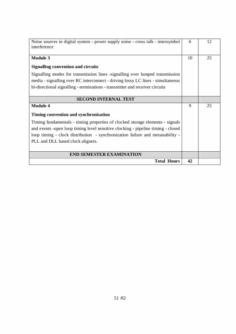
51 /82
Noise sources in digital system - power supply noise - cross talk - intersymbol interference
6 12
Module 3
Signalling convention and circuits Signalling modes for transmission lines -signalling over lumped transmission media - signalling over RC interconnect - driving lossy LC lines - simultaneous bi-directional signalling - terminations - transmitter and receiver circuits
10 25
SECOND INTERNAL TEST Module 4
Timing convention and synchronisation Timing fundamentals - timing properties of clocked storage elements - signals and events -open loop timing level sensitive clocking - pipeline timing - closed loop timing - clock distribution - synchronization failure and metastability - PLL and DLL based clock aligners.
9 25
END SEMESTER EXAMINATION Total Hours 42

52 /82
Course No: 09EC6756
Course Title: MULTIMEDIA COMPRESSION TECHNIQUES
Credits: 3-0-0: 3 Year : 2015
Pre-requisites: Nil
Objective:
Explain the purposes of digital multimedia compression. Define different types of compression: lossless and lossy compression. Examine the theoretical and practical aspects of the text, image, video and audio
compression processes. Describe the data redundancies that may be exploited by different types of
compression algorithms. Address methods in the multimedia compression Huffman coding, DCT-based coding,
motion-compensated prediction coding etc. Describe the existing multimedia compression standards.
Syllabus: Overview of Multimedia compression techniques, Text compression, Audio compression, Video compression Course Outcome: After successful completion of the course, students should be able to:
Understand the characteristics of different media; understand the representations of different multimedia data; understand different data formats; be able to take into considerations in multimedia system designs.
Understand the characteristics of human’s visual system; understand the characteristics of human’s audio system; be able to take into considerations in multimedia techniques design and implementation.
Understand different compression principles; understand different compression techniques; understand different multimedia compression standards; be able to design and develop multimedia systems according to the requirements of multimedia applications.
TEXT BOOKS:
1. Khalid Sayood: Introduction to Data Compression, Morgan Kauffman Harcourt India,
3rd Edition, 2010

53 /82
2. David Salomon: Data Compression – The Complete Reference, Springer Verlag New
York Inc., 4th Edition, 2006.
REFERENCES:
1. Yun Q. Shi, Huifang Sun: Image and Video Compression for Multimedia Engineering -
Fundamentals, Algorithms & Standards, CRC press, 2003.
2. Peter Symes: Digital Video Compression, McGraw Hill Pub., 2004.
3. Mark Nelson: Data compression, BPB Publishers, New Delhi, 2008
4. Mark S. Drew, Ze-Nian Li: Fundamentals of Multimedia, PHI, 1st Edition, 2009.
5. Watkinson, J: Compression in Video and Audio, Focal press, London.1995.
6. Jan Vozer: Video Compression for Multimedia, AP Profes, NewYork, 1995
7. Gonzalez and Woods, Digital Image Processing, 3rd Ed, PHI
In addition, manufacturers Device data sheets and application notes are to be referred to get practical and application oriented information. Internal continuous assessment: 40 marks Internal continuous assessment : Test 1- 15 marks Test 2- 15 marks Assignment/Tutorial-10 marks Total-40marks COURSE PLAN: Course No: 09EC6756 Title: MULTIMEDIA COMPRESSION TECHNIQUES (L-T-P): 3-0-0 Credits: 3
Modules Hours % marks in ESE
Module 1 - Introduction Special features of Multimedia – Graphics and Image Data Representations – Fundamental Concepts in Video and Digital Audio – Storage requirements for multimedia applications -Need for Compression - Taxonomy of compression techniques – Overview of source coding
10 25

54 /82
Text Compression
Compaction techniques – Huffman coding – Adaptive Huffman Coding – Arithmetic coding – Shannon-Fano coding – Dictionary techniques – LZW family algorithms.
Module 2 - IMAGE COMPRESSION Transform Coding – Discrete Cosine Transform(DCT), Quantization and Coding of Transform Coefficients. JPEG Standard – Sub-band coding algorithms:
7 13
FIRST INTERNAL TEST Design of Filter banks – Wavelet based compression: Implementation using filters – EZW, SPIHT coders – JPEG 2000 standard.
6 12
Module 3 - AUDIO COMPRESSION Audio compression techniques - µ- Law and A- Law companding. Frequency domain and filtering – Basic sub-band coding – Application to speech coding – G.722 – Application to audio coding – MPEG audio. Speech compression techniques – LPC and CELP.
10 25
SECOND INTERNAL TEST
Module 4 - VIDEO COMPRESSION Video compression techniques and standards – MPEG Video Coding I: MPEG – 1 and 2 – MPEG Video Coding II: MPEG – 4 and 7 – Motion estimation and compensation techniques – H.261 Standard – DVI technology – Packet Video.
Multimedia Delivery-Multiplexing, Packetization, Time stamping, Synchronization and playback.
9 25
END SEMESTER EXAMINATION Total Hours 42

55 /82
Course No: 09EC6766
Course Title: DESIGN FOR TESTABILITY
Credits: 3-0-0: 3 Year : 2015
Pre-requisites: Nil
Objective:
To improve knowledge in digital testing and design for testability.
To understand ATPG and how to use ATPG Tools.
To understand JTAG scan chain.
To learn the design of memory and logic BIST
To severs as a solid basis for research in testing or fault-tolerant computing.
Syllabus:
Introduction to test and design for Testability Fundamentals: Modeling: Modeling digital
circuits at logic, register and structural models. Levels of Modeling, Logic Simulation Types of
simulation, Delay models, element evaluation, Hazard detection , Gate level event driven
simulation, Logic Fault models, Fault detection and redundancy, Fault equivalence and fault
location.
Testing for single Stuck Faults (SSF): Automated test pattern generation (ATPG/ATG) for
SSFs in combinational and sequential circuits, Functional Testing with specific fault models,
Vector Simulation ATPG Vectors, Formats, Compaction and Compression, Selecting ATPG
Tools.
Design for Testability: Testability tradeoffs and techniques Scan Architectures and testing
Controllability and Observability, Generic Boundary scan, Full integrated scan, storage cells
for scan design, Board level and system level DFT approaches, Boundary scan standards,
Compression Techniques – Syndrome test band signature analysis.
Built in Self Test (BIST):,

56 /82
BIST concepts and test pattern generation , Specific BIST Architectures CSBL, BEST,RTS,
LOCST, STUMPS, CBIST, CEBS,RTD, SST, CATS, CSTP, BILBO. Advanced BIST
concepts and design for self test at Board level
Memory BIST(M BIST):,
Memory test Architectures and Techniques – Introduction to memory test, Types of memories
and integration, embedded memory testing model, Memory test requirement for MBIST.
Embedded core testing Introduction to automatic in circuit testing JTAG testing features.
Course Outcome: After successful completion of the course, students should be able to:
Get knowledge of testability models for combinational and sequential circuits.
Understand the ATPG and ATPG Tools.
Get knowledge of JTAG scan chain and BIST.
Get the solid foundations for research in VLSI testing.
TEXT BOOKS: 1. “Digital systems Testing and testable Design”, Miron Abramovici, Melvin A. Breur,
Arthur D. Friedman, Jaico Publishing House, 2001.
REFERENCES: 1. “Introduction to VLSI Testing”, Englehood cliffs, Robert J. Feugate, Jr., Steven M.
Mentyn, Prentice Hall, 1998. 2. “Design for test for digital IC & Embedded Core Systems”, Alfred Crouch, Prentice
hall.
In addition, manufacturers Device data sheets and application notes are to be referred to get practical and application oriented information. Internal continuous assessment: 40 marks Internal continuous assessment : Test 1- 15 marks Test 2- 15 marks Assignment/Tutorial-10 marks Total-40marks

57 /82
COURSE PLAN: Course No: 09EC6766 Title: DESIGN FOR TESTABILITY (L-T-P): 3-0-0 Credits: 3
Modules Hours % marks in ESE
Module 1
Introduction to test and design for Testability Fundamentals: Modeling:
Modeling digital circuits at logic, register and structural models. Levels of
Modeling, Logic Simulation Types of simulation, Delay models, element
evaluation, Hazard detection , Gate level event driven simulation, Logic Fault
models, Fault detection and redundancy, Fault equivalence and fault location.
10 25
Module 2
Testing for single Stuck Faults (SSF): Automated test pattern generation
(ATPG/ATG) for SSFs in combinational and sequential circuits, Functional
Testing with specific fault models, Vector Simulation ATPG Vectors, Formats,
Compaction and Compression, Selecting ATPG Tools.
9 13
FIRST INTERNAL TEST
Module 3
Design for Testability: Testability tradeoffs and techniques Scan Architectures
and testing Controllability and Observability, Generic Boundary scan, Full
integrated scan, storage cells for scan design, Board level and system level DFT
approaches, Boundary scan standards, Compression Techniques – Syndrome
test band signature analysis.
10 25
SECOND INTERNAL TEST
Module 4
Built in Self Test (BIST):,
BIST concepts and test pattern generation , Specific BIST Architectures CSBL,
BEST,RTS, LOCST, STUMPS, CBIST, CEBS,RTD, SST, CATS, CSTP,
BILBO. Advanced BIST concepts and design for self test at Board level
Memory BIST(M BIST):,
Memory test Architectures and Techniques – Introduction to memory test,
13 25

58 /82
Types of memories and integration, embedded memory testing model, Memory
test requirement for MBIST. Embedded core testing Introduction to automatic
in circuit testing JTAG testing features.
END SEMESTER EXAMINATION Total Hours 42

59 /82
Course No: 09EC6762
Course Title: MINI PROJECT
Credits: 0-0-2: 2 Year : 2015
Pre-requisites: Nil
Objective:
To apply the VLSI design concepts introduced in the courses to a moderately complex embedded system.
Syllabus: The students can select hardware, software or system level mini projects. The mini project can
be implemented using VLSI design/ simulation tools or FPGA which they have studied. A
complete product or project can be selected. The project can be done individually or as a group
of two students.
Course Outcome: After successful completion of the mini project, students should get the necessary confidence to take up bigger embedded challenges
REFERENCES: Manufacturers Device data sheets and application notes are to be referred to get practical and application oriented information. Internal Continuous Assessment: 100 marks
Internal continuous assessment is in the form of evaluation, demonstration, presentation etc. The assessment details are to be announced to the students, right at the beginning of the semester by the teacher.
Attendance & Regularity 20 Marks
Evaluation I 30 Marks
Evaluation II 30 Marks
Assessment by Guide 20 Marks
Total 100 Marks

60 /82
Course No: 09EC6772
Course Title: TESTING & VERIFICATION OF VLSI CIRCUITS - LABORATORY Credits: 0-0-2: 1 Year : 2015
Pre-requisites: Nil
Objective: Objectives:
To understand various types of test benches, random and directed tests.
To learn how to plan, build verification environment for IPs.
To understand the importance of assertion and coverage in RTL verification.
Syllabus: Familiarization of test benches, verification environment of IPs, RTL verification.
Course Outcome:
Understanding of various test benches, and importance of random testing.
Learn how to plan and build verification environment for IPs.
Basic understanding of the necessity of Assertion based and Coverage Driven
Verification.
Text Books:
1. Verilog HDL by Samir Palnitkar.
Reference Books: 1. T. Kropf, "Introduction to Formal Hardware Verification", Springer Verlag, 2000. P.
Rashinkar, Paterson and L. Singh, 2. "System-on-a-Chip Verification-Methodology and Techniques", Kluwer Academic
Publishers, 2001.
Internal continuous assessment: 100 marks Internal continuous assessment : Test 1- 40 marks Test 2- 50 marks Laboratory Experiments & Viva Voce -10 marks Total-100marks

61 /82
COURSE PLAN: Course No: 09EC6772 Title: TESTING & VERIFICATION OF VLSI CIRCUITS - LABORATORY (L-T-P): 0-0-2 Credits: 1
Modules Hours % marks in ESE
Module 1 1. Verilog Simulation and RTL Verification a) Memory b) Clock Divider and Address Counter c) n-Bit Binary Counter and RTL Verification 2. Finite State Machines Implement and Verify Using Verilog File I/O 3. Different types of TBs for memory and adder/subtractor
12 40
FIRST INTERNAL TEST Module 2 1. Basic Verification environment for FIFO/UART
2. Verification Planning for FIFO/UART a) Development of the test cases as per the verification plan b) Generation and Analysis of Code coverage Reports 3. Writing assertions for FIFO
14 60
SECOND INTERNAL TEST Total Hours 28
Internal Continuous Assessment: 100 marks
Internal continuous assessment is in the form of periodical tests. There will be a minimum of two tests per subject. The assessment details are to be announced to the students, right at the beginning of the semester by the teacher.
Mid Term Internal Test 40 Marks
Laboratory Experiments & Viva Voce 10 Marks
Final Internal Test 50 Marks
Total 100 Marks

62 /82
THIRD SEMESTER
09EC77x7 - ELECTIVE IV &
09EC77x7 - ELECTIVE V
Course No: 09EC7717
Course Title: MIXED SIGNAL SYSTEM DESIGN
Credits: 3-0-0: 3 Year : 2015
Pre-requisites: Nil
Objective: To introduce the principles of Analog Mixed Signal System Design. Design and Analysis of Complex Digital and Analog CMOS Circuits to provide a
foundation for more complicated and advanced Designs. To introduce the concept of switched capacitor techniques. To address practical issues in Analog Mixed Signal System Design
Syllabus: PN Junctions, Bipolar Vs Unipolar Devices, MOS Transistor operation, CMOS Logic implementation basics, TG based implementation of multiplexers, de-multiplexers, encoders, decoders, ALU, Comparator, Parity generator, Timer, PWM,SRAM and DRAM,CAM, Analog Sub circuits, Ideal Operational Amplifier, Inverting and Non-inverting configuration Differential amplifier basics, VCO, PLL, Data Converters, DAC, ADC, Over sampling Data Converters.
Course Outcome: After successful completion of the course, students should be able to: Detailed knowledge of static and dynamic behavior of CMOS logic. Detailed understanding of CMOS Digital Subsystem Design. Timing analysis and synchronization of digital design. Basic understanding of Analog circuit building blocks. Detailed understanding of Analog Mixed Signal Circuit Design. Detailed Understanding of Data Converters.

63 /82
TEXT BOOKS:
1. CMOS Analog Circuit Design, 2nd edition; by: Allen, Phillip E, Holberg , Douglas R, Oxford University Press, (Indian Edition).
2. D A John, Ken Martin, Analog Integrated Circuit Design, 1st Edition, John Wiley.
REFERENCES: 1. Ken Martin, Digital Integrated Circuit Design, John Wiley 2. Gray Paul R, Meyer, Robert G, Analysis and Design of Analog Integrated Circuits, 3rd
edition, John Wiley & Sons. 3. Sedra & Smith, Microelectronics Circuits, 5th Edition, Oxford University Press, (Indian
Edition) 4. Jan M. Rabaey, Anantha Chadrakasan, B. Nikolic ,Digital Integrated Circuits – A
Design Perspective 2nd Edition, Prentice Hall of India (Eastern Economy Edition). 5. Sung-Mo Kang, Yusuf Leblebici, CMOS Digital Integrated Circuits Analysis &
Design,2nd Ed, Tata McGraw Hill In addition, manufacturers Device data sheets and application notes are to be referred to get practical and application oriented information. Internal continuous assessment: 40 marks Internal continuous assessment : Test 1- 15 marks Test 2- 15 marks Assignment/Tutorial-10 marks Total-40marks COURSE PLAN: Course No: 09EC7717 Title: MIXED SIGNAL SYSTEM DESIGN (L-T-P): 3-0-0 Credits: 3
Modules Hours % marks in ESE
Module 1 Introduction
PN Junctions, Bipolar Vs Unipolar Devices, MOS Transistor operation, MOS Transistor as a Switch, NMOS ,PMOS and CMOS Switches, CMOS Inverter AC and DC Characteristics, Analog Signal Processing, Example of Analog Mixed Signal Circuit Design
10 25

64 /82
Module 2 Digital Sub Circuits
CMOS Logic implementation basics- Logic gates and Flip flops –Transmission Gates, TG based implementation of multiplexers, de-multiplexers, encoders, decoders.
7 13
FIRST INTERNAL TEST Digital Circuits like ALU, Comparator, Parity generator, Timer, PWM,SRAM and DRAM,CAM
6 12
Module 3 Analog Sub circuits
Ideal Operational Amplifier, Inverting and Non-inverting configuration Differential amplifier basics, VCO, PLL, Comparator characteristics, two stage open loop comparator ,Switched capacitor fundamentals, Switched capacitor amplifier
10 25
SECOND INTERNAL TEST Module 4
Module 4 Data Converters
DAC : Static &Dynamic Charatersitics,1 Bit DAC, String DAC, Fully Decoded DAC,PWM DAC, Current scaling, voltage scaling DACs ADC : Static &Dynamic Characteristics, Nyquist Criteria , Sample & Hold Circuit ,Quantization error, Concept of over sampling, Counting ADC, Tracking ADC, Successive approximation ADC, Flash ADC, Dual Slope ADC Over sampling Data Converters : Over sampling fundamentals, Delta –Sigma Converter basics, Δ ∑ Modulator
9 25
END SEMESTER EXAMINATION Total Hours 42

65 /82
Course No: 09EC7727
Course Title: FPGA ARCHITECTURE AND APPLICATIONS
Credits: 3-0-0: 3 Year : 2015
Pre-requisites: Nil
Objective:
To understand the basic principle of Programmable Logic Devices and applications.
To learn contemporary FPGA Architectures from Xilinx and Altera.
To understand the programming of combinational ,sequential circuits and FSMs on
FPGAs.
To learn how to prototype a system on FPGA.
Syllabus: Programmable logic Devices, Applications and Implementation of MSI circuits using
Programmable logic Devices, FPGAs, mapping for FPGAs, Case studies Xilinx XC4000 &
ALTERA’s FLEX 8000/10000 FPGAs, Introduction to advanced FPGAs: Xilinx Virtex and
ALTERA Stratix, Finite State Machines (FSM), System Level Design, Case studies
Course Outcome: After successful completion of the course, students should be able to:
Understanding of basic PLD architecture and applications.
Knowledge of contemporary FPGA architectures.
Basic understanding of how circuits are programmed on FPGA.
Knowledge of how to prototype a system on FPGA.
TEXT BOOKS: 1. Field Programmable Gate Array Technology - S. Trimberger, Edr, 1994, Kluwer Academic
Publications.
REFERENCES:
1. Engineering Digital Design - RICHARD F.TINDER, 2nd Edition, Academic press.

66 /82
2. Fundamentals of logic design-Charles H. Roth, 4th Edition Jaico Publishing House. 3. Digital Design Using Field Programmable Gate Array, P.K. Chan & S. Mourad, 1994,
Prentice Hall. Field programmable gate array, S. Brown, R.J. Francis, J. Rose, Z.G. Vranesic, 2007, BS
In addition, manufacturers Device data sheets and application notes are to be referred to get practical and application oriented information. Internal continuous assessment: 40 marks Internal continuous assessment : Test 1- 15 marks Test 2- 15 marks Assignment/Tutorial-10 marks Total-40marks COURSE PLAN: Course No: 09EC7727 Title: FPGA ARCHITECTURE AND APPLICATIONS (L-T-P): 3-0-0 Credits: 3
Modules Hours % marks in ESE
Module 1
Programmable logic Devices: ROM, PLA, PAL, CPLD, FPGA Features,
Architectures and Programming.
Applications and Implementation of MSI circuits using Programmable logic
Devices.
10 25
Module 2
FPGAs: Field Programmable Gate Arrays- Logic blocks, routing architecture,
design flow, technology
mapping for FPGAs, Case studies Xilinx XC4000 & ALTERA’s FLEX
8000/10000 FPGAs.
7 13
FIRST INTERNAL TEST
Introduction to advanced FPGAs: Xilinx Virtex and ALTERA Stratix
6 12

67 /82
Module 3
Finite State Machines (FSM): Top Down Design, State Transition Table, State
assignments for FPGAs,Realization of state machine charts using PAL,
Alternative realization for state machine charts using microprogramming,
linked state machine, encoded state machine.
10 25
SECOND INTERNAL TEST
Module 4
System Level Design: Controller, data path designing, Functional partition,
Digital front end digital design tools for FPGAs.
System level design using mentor graphics/Xilinx EDA tool (FPGA
Advantage/Xilinx ISE), Design flow using FPGAs.
Case studies: Design considerations using FPGAs of parallel adder cell, parallel
adder sequential circuits, counters, multiplexers, parallel controllers.
9 25
END SEMESTER EXAMINATION Total Hours 42

68 /82
Course No: 09EC7737
Course Title: WIRELESS TECHNOLOGIES
Credits: 3-0-0: 3 Year : 2015
Pre-requisites: Nil
Objective:
This subject is framed to set the required background in wireless communication. Being
the backbone for all the IT based developments; Wireless Technology has seen
tremendous growth in the past decade. There are new techniques and protocols
emerging from time-to-time to cater the requirements of this rapidly growing area.
The subject will cover from rf fundamentals to the topics like celluar, WiFi, WPN and
WSN technologies.
The treatment would look at current and upcoming wireless communications
technologies for various wireless accesses.
Syllabus:
Radio Frequency (RF) Fundamentals, Spread Spectrum Concepts, RF Antenna Concepts,
Cellular Standards, WLAN, Wi-Fi Organizations and Standards, Wi-Fi Hardware & Software,
WSN & WPN, IEEE 802.15 standards, ZigBee, Sub1GHz, Sensor Networks, Interfacing
problems and co-existence strategies in Sensor Networks, Routing protocols in Wireless
Sensor Networks.
Course Outcome:
After successful completion of the course, students should be able to:
Understand the different wireless technologies available today.
Understand the basics of embedded wireless application development.
TEXT BOOKS:
1. Wireless Communications – Principles and Practice; by Theodore S Rappaport, Pearson Education Pte. Ltd., Delhi
2. Wireless Communications and Networking; By: Stallings, William; Pearson Education Pte. Ltd., Delhi

69 /82
REFERENCES: 1. Bluetooth Revealed; By: Miller, Brent A, Bisdikian, Chatschik; Addison Wesley
Longman Pte Ltd., Delhi 2. Wilson , “Sensor Technology hand book,” Elsevier publications 2005. 3. Andrea Goldsmith, “Wireless Communications,” Cambridge University Press, 2005 4. Mobile and Personal Communications Services and Systems; 1st Edition; By: Raj
Pandya; PHI, New Delhi 5. Fundamentals of Wireless Communication by Tse David and Viswanath Pramod,
Cambridge University press, Cambridge 6. Mobile Communications; By: Schiller, Jochen H; Addison Wesley Longman Pte Ltd.,
Delhi 7. 3G Networks: Architecture, protocols and procedures based on 3GPP specifications for
UMTS WCDMA networks, By Kasera, Sumit, Narang, and Nishit, TATA MGH, New Delhi
8. Wireless Sensor Networks: information processing by approach, ZHAO, FENG, GUIBAS and LEONIDAS J, ELSEVIER, New Delhi
9. Holger Karl and Andreas Wiilig, “Protocols and Architectures for Wireless Sensor Networks” John Wiley & Sons Limited 2008.
In addition, manufacturers Device data sheets and application notes are to be referred to get practical and application oriented information. Internal continuous assessment: 40 marks Internal continuous assessment : Test 1- 15 marks Test 2- 15 marks Assignment/Tutorial-10 marks Total-40marks COURSE PLAN: Course No: 09EC7737 Title: WIRELESS TECHNOLOGIES (L-T-P): 3-0-0 Credits: 3
Modules Hours % marks in ESE
Module 1 - RF Basics:
Radio Frequency (RF) Fundamentals: Introduction to RF & Wireless Communications Systems, RF and Microwave Spectral Analysis, Communication Standards, Understanding RF & Microwave Specifications. Spectrum Analysis of RF Environment, Protocol Analysis of RF Environment, Units of RF measurements, Factors affecting network range
10 25

70 /82
and speed, Environment, Line-of-sight, Interference, Defining differences between physical layers- OFDM, HR/DSSS,MIMO Spread Spectrum Concepts: OFDM & HR/DSSS channels, Co-location of HR/DSSS and OFDM systems, Adjacent-channel and co-channel interference, WLAN / WPAN co-existence, CSMA/CA operations RF Antenna Concepts: Passive gain, Beam widths, Simple diversity, Polarization, Antenna Mounting, Wireless Antennas and Accessories, RF cables, RF connectors, Lightning arrestors and grounding rods
Module 2 – Cellular Standards
Cellular carriers and Frequencies, Channel allocation, Cell coverage, Cell Splitting, Microcells, Picocells, Handoff
7 13
FIRST INTERNAL TEST 1st, 2nd, 3rd and 4th Generation Cellular Systems (GSM, CDMA,IS-95, GPRS, EDGE,UMTS, EVDO, CDMA2000), Mobile IP, WCDMA
6 12
Module 3 – WLAN Wi-Fi Organizations and Standards: Regulatory Bodies, IEEE, Wi-Fi Alliance, WLAN Connectivity, WLAN QoS & Power-Save, IEEE 802.11 Standards,802.11-2007,802.11a/b/g, 802.11e/h/I,802.11n
Wi-Fi Hardware & Software: Access Points, WLAN Routers, WLAN Bridges, WLAN Repeaters, WLAN Controllers/Switches, Direct-connect Aps, Distributed-connect Aps, PoE Infrastructure, Midspan, Endpoint, Client hardware and software, Antenna types and uses
Wi-Fi Security concepts, Wi-Fi Applications
10 25
SECOND INTERNAL TEST
Module 4 – WSN & WPN
Wireless Personal Area Networks, Bluetooth, Bluetooth Standards, BlueTooth Protocol Architecture,UWB, IEEE 802.15 standards, ZigBee, Sub1GHz, Sensor Networks, Interfacing problems and co-existence strategies in Sensor Networks, Routing protocols in Wireless Sensor Networks.
9 25
END SEMESTER EXAMINATION Total Hours 42
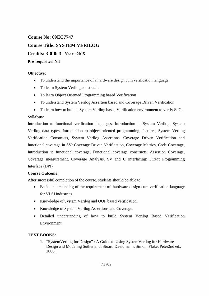
71 /82
Course No: 09EC7747
Course Title: SYSTEM VERILOG
Credits: 3-0-0: 3 Year : 2015
Pre-requisites: Nil
Objective:
To understand the importance of a hardware design cum verification language.
To learn System Verilog constructs.
To learn Object Oriented Programming based Verification.
To understand System Verilog Assertion based and Coverage Driven Verification.
To learn how to build a System Verilog based Verification environment to verify SoC.
Syllabus: Introduction to functional verification languages, Introduction to System Verilog, System
Verilog data types, Introduction to object oriented programming, features, System Verilog
Verification Constructs, System Verilog Assertions, Coverage Driven Verification and
functional coverage in SV: Coverage Driven Verification, Coverage Metrics, Code Coverage,
Introduction to functional coverage, Functional coverage constructs, Assertion Coverage,
Coverage measurement, Coverage Analysis, SV and C interfacing: Direct Programming
Interface (DPI)
Course Outcome: After successful completion of the course, students should be able to:
Basic understanding of the requirement of hardware design cum verification language
for VLSI industries.
Knowledge of System Verilog and OOP based verification.
Knowledge of System Verilog Assertions and Coverage.
Detailed understanding of how to build System Verilog Based Verification
Environment.
TEXT BOOKS:
1. “SystemVerilog for Design” : A Guide to Using SystemVerilog for Hardware Design and Modeling Sutherland, Stuart, Davidmann, Simon, Flake, Peter2nd ed., 2006.
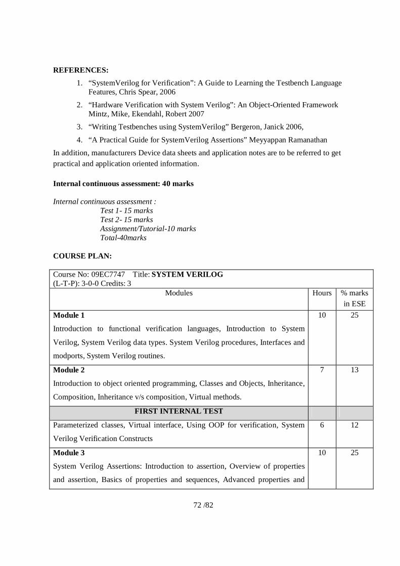
72 /82
REFERENCES: 1. “SystemVerilog for Verification”: A Guide to Learning the Testbench Language
Features, Chris Spear, 2006 2. “Hardware Verification with System Verilog”: An Object-Oriented Framework
Mintz, Mike, Ekendahl, Robert 2007 3. “Writing Testbenches using SystemVerilog” Bergeron, Janick 2006,
4. “A Practical Guide for SystemVerilog Assertions” Meyyappan Ramanathan In addition, manufacturers Device data sheets and application notes are to be referred to get practical and application oriented information. Internal continuous assessment: 40 marks Internal continuous assessment : Test 1- 15 marks Test 2- 15 marks Assignment/Tutorial-10 marks Total-40marks COURSE PLAN: Course No: 09EC7747 Title: SYSTEM VERILOG (L-T-P): 3-0-0 Credits: 3
Modules Hours % marks in ESE
Module 1
Introduction to functional verification languages, Introduction to System
Verilog, System Verilog data types. System Verilog procedures, Interfaces and
modports, System Verilog routines.
10 25
Module 2
Introduction to object oriented programming, Classes and Objects, Inheritance,
Composition, Inheritance v/s composition, Virtual methods.
7 13
FIRST INTERNAL TEST
Parameterized classes, Virtual interface, Using OOP for verification, System
Verilog Verification Constructs
6 12
Module 3
System Verilog Assertions: Introduction to assertion, Overview of properties
and assertion, Basics of properties and sequences, Advanced properties and
10 25

73 /82
sequences, Assertions in design and formal verification, some guidelines in
assertion writing.
SECOND INTERNAL TEST
Module 4
Coverage Driven Verification and functional coverage in SV: Coverage Driven
Verification, Coverage Metrics, Code Coverage, Introduction to functional
coverage, Functional coverage constructs, Assertion Coverage, Coverage
measurement, Coverage Analysis
SV and C interfacing: Direct Programming Interface (DPI)
9 25
END SEMESTER EXAMINATION Total Hours 42
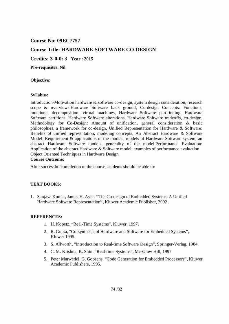
74 /82
Course No: 09EC7757
Course Title: HARDWARE-SOFTWARE CO-DESIGN
Credits: 3-0-0: 3 Year : 2015
Pre-requisites: Nil
Objective: Syllabus: Introduction-Motivation hardware & software co-design, system design consideration, research scope & overviews Hardware Software back ground, Co-design Concepts: Functions, functional decomposition, virtual machines, Hardware Software partitioning, Hardware Software partitions, Hardware Software alterations, Hardware Software tradeoffs, co-design, Methodology for Co-Design: Amount of unification, general consideration & basic philosophies, a framework for co-design, Unified Representation for Hardware & Software: Benefits of unified representation, modeling concepts, An Abstract Hardware & Software Model: Requirement & applications of the models, models of Hardware Software system, an abstract Hardware Software models, generality of the model Performance Evaluation: Application of the abstract Hardware & Software model, examples of performance evaluation Object Oriented Techniques in Hardware Design Course Outcome: After successful completion of the course, students should be able to: TEXT BOOKS: 1. Sanjaya Kumar, James H. Ayler “The Co-design of Embedded Systems: A Unified
Hardware Software Representation”, Kluwer Academic Publisher, 2002 .
REFERENCES:
1. H. Kopetz, “Real-Time Systems”, Kluwer, 1997.
2. R. Gupta, “Co-synthesis of Hardware and Software for Embedded Systems”, Kluwer 1995.
3. S. Allworth, “Introduction to Real-time Software Design”, Springer-Verlag, 1984. 4. C. M. Krishna, K. Shin, “Real-time Systems”, Mc-Graw Hill, 1997
5. Peter Marwedel, G. Goosens, “Code Generation for Embedded Processors”, Kluwer Academic Publishers, 1995.

75 /82
In addition, manufacturers Device data sheets and application notes are to be referred to get practical and application oriented information. Internal continuous assessment: 40 marks Internal continuous assessment : Test 1- 15 marks Test 2- 15 marks Assignment/Tutorial-10 marks Total-40marks COURSE PLAN: Course No: 09EC7757 Title: HARDWARE-SOFTWARE CO-DESIGN (L-T-P): 3-0-0 Credits: 3
Modules Hours % marks in ESE
Module 1
Introduction: Motivation hardware & software co-design, system design
consideration, research scope & overviews
Hardware Software back ground: Embedded systems, models of design
representation, the virtual machine hierarchy, the performance3 modeling,
Hardware Software development
10 25
Module 2
Co-design Concepts: Functions, functional decomposition, virtual machines,
Hardware Software partitioning,
7 13
FIRST INTERNAL TEST
Hardware Software partitions, Hardware Software alterations, Hardware
Software tradeoffs, co-design.
6 12
Module 3
Methodology for Co-Design: Amount of unification, general consideration &
basic philosophies, a framework for co-design
10 25

76 /82
Unified Representation for Hardware & Software: Benefits of unified
representation, modeling concepts.
An Abstract Hardware & Software Model: Requirement & applications of the
models, models of Hardware Software system, an abstract Hardware Software
models, generality of the model
Performance Evaluation: Application of t he abstract Hardware & Software
model, examples of performance evaluation
SECOND INTERNAL TEST
Module 4
Object Oriented Techniques in Hardware Design: Motivation for object
oriented technique, data types, modeling hardware components as classes,
designing specialized components, data decomposition, Processor example.
9 25
END SEMESTER EXAMINATION
Total Hours 42

77 /82
Course No: 09EC7767
Course Title: VLSI SIGNAL PROCESSING
Credits: 3-0-0: 3 Year : 2015
Pre-requisites: Nil
Objective:
To cover techniques for designing efficient DSP architectures. To realize DSP architectures that will process high throughout data end/or require less
power and / or less chip area. To learn a complete DSP system and fundamentals of pipelining and parallel
processing on FIR filters To study the concepts of retiming, unfolding, transforms and rank order filters. To study different bit level architectures and their complexities To realize array signal processing structures like spatial filter
Syllabus:
Graphical representation of DSP algorithms, Dataflow and control flow, Unfolding, Folding, Design of VLSI Architectures for Digital Signal Processing, Speed-Area-Power tradeoff issues related to mixed signal design and SoC, Filter structures, Transform structures, Data Flow and Control flow issues, Modern DSP algorithms, VLSI Architecture development for JPEG2000 video CODEC and performance comparisons
Course Outcome:
After successful completion of the course, students should be able to:
Understand various signal processing algorithms that can be designed and applied on application specific VLSI architecture
Have the knowledge on introducing pipelining, parallism, in place memory and high speed multipliers, used to improve the efficiency of DSP processors
Analyze different number representations, arithmetic based binary representations and complexities involved in it for easier numerical computations on processors.
Gain minimum knowledge to find solution for any research queries on DSP processors.
TEXT BOOKS: 1. VLSI Signal Processing Systems - Keshab K Parhi, John Wiley and Son's, NY 1999.

78 /82
2. Architectures for Digital Signal Processing - Peter Prissch, John Wiley and Son's NY 1998.
REFERENCES: 1. Introduction to Data Compression, 2nd Edition - Khalid Sayood, Harcourt India, New
Delhi, 2000.
In addition, manufacturers Device data sheets and application notes are to be referred to get practical and application oriented information. Internal continuous assessment: 40 marks Internal continuous assessment : Test 1- 15 marks Test 2- 15 marks Assignment/Tutorial-10 marks Total-40marks COURSE PLAN: Course No: 09EC7767 Title: VLSI SIGNAL PROCESSING (L-T-P): 3-0-0 Credits: 3
Modules Hours % marks in ESE
Module 1:
Graphical representation of DSP algorithms, Dataflow and control flow. Introduction to Pipelining and Parallel Processing, Parallel pipelined design of DSP Algorithms. Retiming: Introduction, Definition and properties, Solving system of inequalities, retiming techniques.
Unfolding Introduction, An algorithms for unfolding, Properties of unfolding, Critical path, unfolding and retiming Application of unfolding.
Folding: Introduction Folding Transformation, Register Minimization Techniques, Register minimization in folded architectures
10 25
Module 2:
Design of VLSI Architectures for Digital Signal Processing: Architectural Design at Register Transfer Level, Design of Data path elements, Control structures
7 13

79 /82
FIRST INTERNAL TEST
Testable and self-reconfigurable fault-tolerant structures. Speed-Area-Power tradeoff issues related to mixed signal design and SoC.
6 12
Module 3 Filter structures, Transform structures, Data Flow and Control flow issues. Array processing approaches to DSP solutions. Introduction to spatial filters. Development of VLSI architecture for spatial filter.
10 25
SECOND INTERNAL TEST Module 4 Modern DSP algorithms (Audio, Video and Multimedia) and development of new computational and arithmetic building blocks. VLSI Architecture development for JPEG2000 video CODEC and performance comparisons.
9 25
END SEMESTER EXAMINATION Total Hours 42

80 /82
Course No: 09EC7763
Course Title: SEMINAR
Credits: 0-0-2: 2 Year : 2015
Pre-requisites: Nil
Objective: To assess the debating capability of the student to present a technical topic. Also to impart training to students to face audience and present their ideas and thus creating in them self esteem and courage that are essential for engineers. Syllabus: Individual students are required to choose a topic of their interest from VLSI Systems related topics preferably from outside the M.Tech syllabus and give a seminar on that topic about 15 minutes. A committee consisting of at least three faculty members (preferably specialized VLSI) shall assess the presentation of the seminar and award marks to the students. Each student shall submit two copies of a write up of his/her seminar topic. One copy shall be returned to the student after duly certifying it by the chairman of the assessing committee and the other will be kept in the departmental library. Internal continuous assessment marks are awarded based on the relevance of the topic, presentation skill, quality of the report and participation. Course Outcome: After successful completion of the seminar, students shall be able to
Understand technical articles in peer reviewed journals and conferences Analyze and present advanced topics in Embedded Systems Their communication, presentation skills etc. shall be improved and shall be ready for
technical paper writing. Internal continuous assessment: 100 marks Subject Relevance : 10 marks
Concept/ Knowledge in the topic : 20 marks
Presentation : 40 marks
Report : 30 marks
Total marks : 100 marks
81 /82
Course No: 09EC7783
Course Title: MASTER RESEARCH PROJECT PHASE I
Credits: 0-0-16: 6 Year : 2015
Pre-requisites: Nil
Objective:
To improve the professional competency and research aptitude by touching the areas which otherwise not covered by theory or laboratory classes. The project work aims to develop the work practice in students to apply theoretical and practical tools/techniques to solve real life problems related to industry and current research.
Syllabus: The project work can be a design project/experimental project and/or computer simulation project on any of the topics in electronics design related topics. The project work is allotted individually on different topics. The students shall be encouraged to do their project work in the parent institute itself. If found essential, they may be permitted to continue their project outside the parent institute, subject to the conditions of M.Tech regulations. Department will constitute an Evaluation Committee to review the project work. The Evaluation committee shall be headed by the head of the department with two other faculty members in the area of the project, of which one shall be the project supervisor. The student is required to undertake the master research project phase 1 during the third semester and the same is continued in the 4thsemester (Phase 2). Phase 1 consist of preliminary thesis work, two reviews of the work and the submission of preliminary report. First review would highlight the topic, objectives, methodology and expected results. Second review evaluates the progress of the work, preliminary report and scope of the work which is to be completed in the 4th semester. The Evaluation committee consists of at least three faculty members of which internal guide and another expert in the specified area of the project shall be two essential members. Course Outcome: After successful completion of the project phase I, students should be able to:
Formulate a research problem and perform literature review systematically carrying out a research and write technical reports
Internal Continuous assessment: 50 Marks
Supervisor/ Guide Evaluation Committee
Project Review 20 Marks 30 Marks

82 /82
FOURTH SEMESTER
Course No: 09EC7784
Course Title: MASTER RESEARCH PROJECT PHASE II
Credits: 0-0-24: 12 Year : 2015
Pre-requisites: Nil
Objective:
To improve the professional competency and research aptitude by touching the areas which otherwise not covered by theory or laboratory classes. The project work aims to develop the work practice in students to apply theoretical and practical tools/techniques to solve real life problems related to industry and current research.
Syllabus: Masters Research project phase-II is a continuation of project phase-I started in the third semester. Before the end of the fourth semester, there will be two reviews, one at middle of the fourth semester and other towards the end. In the first review, progress of the project work done is to be assessed. In the second review, the complete assessment (quality, quantum and authenticity) of the Thesis is to be evaluated. Both the reviews should be conducted by guide and Evaluation committee. This would be a pre qualifying exercise for the students for getting approval for the submission of the thesis. At least one technical paper is to be prepared for possible publication in journal or conferences. The technical paper is to be submitted along with the thesis. The final evaluation of the project will be external evaluation. Course outcome: The students who successfully complete this course will have the demonstrated capability to
Formulate a research problem in embedded systems area Systematically carrying out a research Write technical reports and research publications Publish research findings
Internal Continuous assessment: 100 Marks
Supervisor/ Guide External Expert Evaluation Committee
Project Review 30 Marks 30 Marks 40 Marks


](https://img.dokumen.tips/doc/110x75/55cf8fe1550346703ba0ce6f/vlsi-technologymtech-1-1unit-3.jpg)