Embed Size (px)
Citation preview

Current feedback operational amplifiers as fast charge sensitive preamplifiers for
photomultiplier read out
This article has been downloaded from IOPscience. Please scroll down to see the full text article.
2011 JINST 6 P05004
(http://iopscience.iop.org/1748-0221/6/05/P05004)
Download details:
IP Address: 149.132.2.36
The article was downloaded on 09/05/2011 at 12:44
Please note that terms and conditions apply.
View the table of contents for this issue, or go to the journal homepage for more
Home Search Collections Journals About Contact us My IOPscience

2011 JINST 6 P05004
PUBLISHED BY IOP PUBLISHING FOR SISSA
RECEIVED: October 25, 2010REVISED: April 8, 2011
ACCEPTED: May 2, 2011PUBLISHED: May 9, 2011
Current feedback operational amplifiers as fastcharge sensitive preamplifiers for photomultiplierread out
A. Giachero, a,b C. Gotti, a,c,1 M. Maino a,b and G. Pessina a,b
aINFN — Sezione di Milano-Bicocca,I-20126, Milano, Italy
bDip. di Fisica, Universita degli Studi di Milano-Bicocca,I-20126, Milano, Italy
cDip. Elettronica e TLC, Universita degli Studi di Firenze,I-50139, Firenze, Italy
E-mail: [email protected]
ABSTRACT: Fast charge sensitive preamplifiers were built using commercial current feedback op-erational amplifiers for fast read out of charge pulses from aphotomultiplier tube. Current feedbackopamps prove to be particularly well suited for this application where the charge from the detectoris large, of the order of one million electrons, and high timing resolution is required. A proper cir-cuit arrangement allows very fast signals, with rise times down to one nanosecond, while keepingthe amplifier stable. After a review of current feedback circuit topology and stability constraints,we provide a ”recipe” to build stable and very fast charge sensitive preamplifiers from any currentfeedback opamp by adding just a few external components. Thenoise performance of the circuittopology has been evaluated and is reported in terms of equivalent noise charge.
KEYWORDS: Analogue electronic circuits; Front-end electronics fordetector readout
1Corresponding author.
c© 2011 IOP Publishing Ltd and SISSA doi:10.1088/1748-0221/6/05/P05004

2011 JINST 6 P05004
Contents
1 Introduction to current feedback opamps (CFOAs) 1
2 Loop gain calculation in the current feedback topology 3
3 Capacitive feedback and CFOAs 5
4 The CFOA as a charge sensitive preamplifier 6
5 The “recipe” 135.1 Choosing the CFOA 135.2 Gain 145.3 Fall time 155.4 Stability 15
6 Noise performance and equivalent noise charge 15
1 Introduction to current feedback opamps (CFOAs)
When dealing with high frequency applications requiring bandwidth above the hundred MHz range,most voltage feedback operational amplifiers (VFOAs) cannot be used. This is simply because theirmaximum bandwidth is often below this frequency range. Eventhe fastest VFOAs which can reachthese frequencies at unity gain are not useful because the requirement of gain reduces the availablebandwidth due to the well-known ”gain-bandwidth product” tradeoff. Under compensated opampsare another option, but the amplifier bandwidth and stability turn out to be highly dependent on thedetector capacitance. Thus it is difficult to use commercialVFOAs in building fast charge sensitivepreamplifiers because both gain and high bandwidths are usually required.
In recent years, current feedback operational amplifiers (CFOAs) have been introduced. Thisopamp topology allows for a wide bandwidth, absence of slew rate limitation, and above all, es-sentially the absence of a gain-bandwidth product limit. This occurs because the bandwidth of thecurrent feedback topology, in a first order analysis, is independent of gain and only depends onthe value of the feedback resistor. Thus CFOAs allow any amplification factor without the corre-sponding bandwidth narrowing of a traditional VFOA. The tradeoff is that CFOAs have poor DCprecision and require more effort to achieve closed loop stability. For a broader introduction oncurrent feedback operational amplifiers, we refer to [1–4].
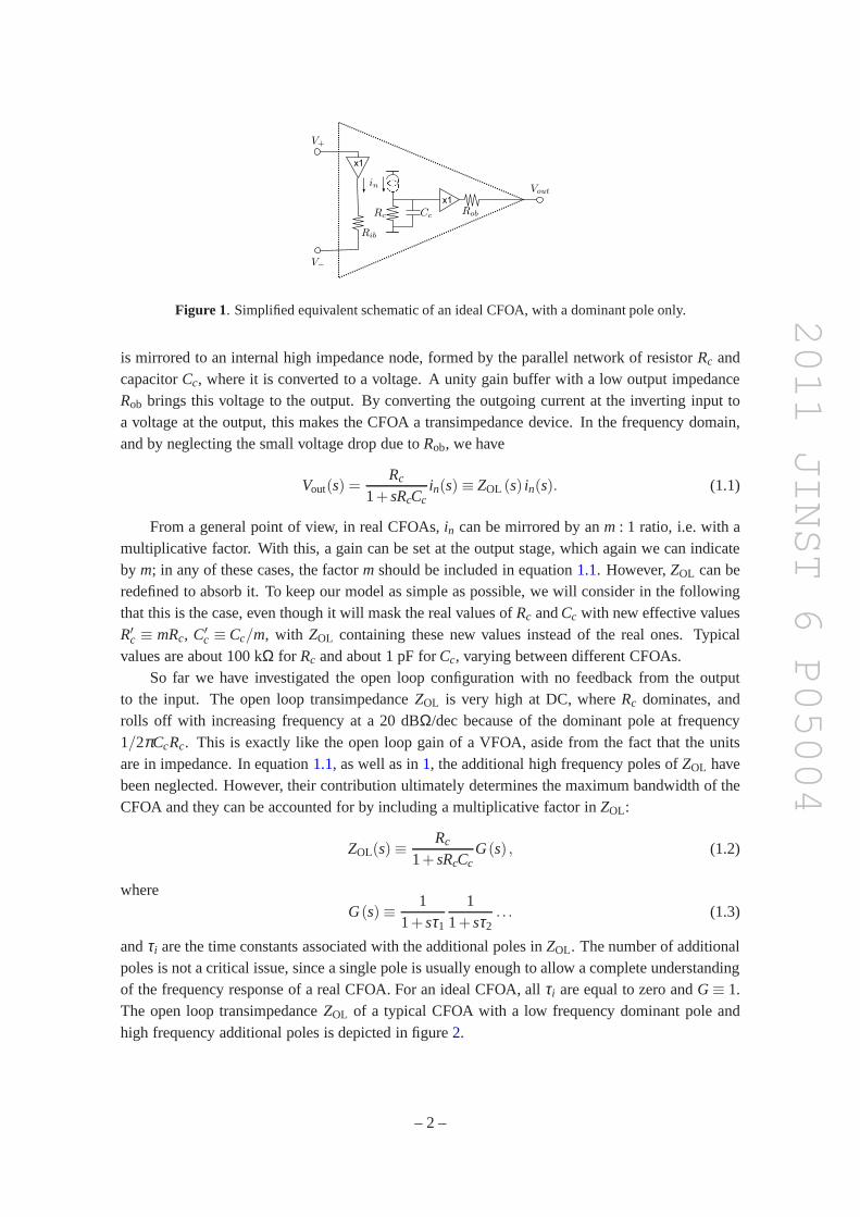
Figure1 shows the simplified model of a CFOA. The non-inverting inputhas high impedance,as with VFOAs, and its voltage is buffered to the inverting input, forcing a zero voltage differencebetween the two. The inverting input is thus a low impedance node (unlike the inverting input ofa VFOA) whose impedance we denote byRib. The currentin flowing out of the inverting input
– 1 –
2011 JINST 6 P05004
x1
x1
Figure 1. Simplified equivalent schematic of an ideal CFOA, with a dominant pole only.
is mirrored to an internal high impedance node, formed by theparallel network of resistorRc andcapacitorCc, where it is converted to a voltage. A unity gain buffer with alow output impedanceRob brings this voltage to the output. By converting the outgoing current at the inverting input toa voltage at the output, this makes the CFOA a transimpedancedevice. In the frequency domain,and by neglecting the small voltage drop due toRob, we have
Vout(s) =Rc
1+sRcCcin(s) ≡ ZOL (s) in(s). (1.1)
From a general point of view, in real CFOAs,in can be mirrored by anm : 1 ratio, i.e. with amultiplicative factor. With this, a gain can be set at the output stage, which again we can indicateby m; in any of these cases, the factorm should be included in equation1.1. However,ZOL can beredefined to absorb it. To keep our model as simple as possible, we will consider in the followingthat this is the case, even though it will mask the real valuesof Rc andCc with new effective valuesR′
c ≡ mRc, C′c ≡ Cc/m, with ZOL containing these new values instead of the real ones. Typical
values are about 100 kΩ for Rc and about 1 pF forCc, varying between different CFOAs.So far we have investigated the open loop configuration with no feedback from the output
to the input. The open loop transimpedanceZOL is very high at DC, whereRc dominates, androlls off with increasing frequency at a 20 dBΩ/dec because of the dominant pole at frequency1/2πCcRc. This is exactly like the open loop gain of a VFOA, aside from the fact that the unitsare in impedance. In equation1.1, as well as in1, the additional high frequency poles ofZOL havebeen neglected. However, their contribution ultimately determines the maximum bandwidth of theCFOA and they can be accounted for by including a multiplicative factor inZOL:
ZOL(s) ≡Rc
1+sRcCcG(s) , (1.2)
whereG(s) ≡ 1
1+sτ1
11+sτ2
. . . (1.3)
andτi are the time constants associated with the additional polesin ZOL. The number of additionalpoles is not a critical issue, since a single pole is usually enough to allow a complete understandingof the frequency response of a real CFOA. For an ideal CFOA, all τi are equal to zero andG≡ 1.The open loop transimpedanceZOL of a typical CFOA with a low frequency dominant pole andhigh frequency additional poles is depicted in figure2.
– 2 –

2011 JINST 6 P05004
dB
Frequencydominant
pole
higher order
pole(s)
-45°
-90°
-135°
0°
Figure 2. Magnitude and phase of the open loop transimpedance of a typical CFOA, with a low frequencydominant pole and high frequency additional poles.
x1
x1
Figure 3. The CFOA buffer: schematic.
The fact that the output has the same sign of the currentin, as can be seen from equation1.1,allows application of negative feedback as is commonly donefor VFOAs. By putting a resistorfrom the output to the input, one obtains the closed loop structure depicted in figure3. In thiscircuit the small resistancesRib and Rob can be neglected, because they have very small valuesand are in series withRf . This circuit is a voltage follower, i.e. a buffer, and is thesame as theVFOA configuration. However, contrasting with the VFOA case, the output cannot be shortedto the inverting input. For CFOAs to be stable, a minimum value of resistive feedback is alwaysrequired. If the value ofRf in figure3 is less than a minimum value (usually around a few hundredOhms depending on the specific CFOA), the CFOA will oscillate. To understand why this happens,a bit of insight on the exact behavior of the feedback structure is necessary and is the subject of thenext section.
2 Loop gain calculation in the current feedback topology
As common practice in the study of operational amplifier circuits and feedback structures in gen-eral, the loop gain plays a crucial role (see for instance [5]).
– 3 –

2011 JINST 6 P05004
x1
x1
Figure 4. The CFOA buffer: loop gain calculation.
The loop gain is defined as the gain of a signal injected at any node of the feedback loopresulting from traveling all the way around the loop and backto the starting node. In the case ofoperational ampliers, the easiest way to calculate the loopgain is to break the loop at the output ofthe opamp and null the input sources, as depicted in figure4 for the CFOA buffer. By injecting thetest signalVT , we can calculate the voltageVR generated at the output of the opamp. The loop gainis the ratioT =VR/VT . Since the circuit is linear,1 T does not depend onVT . Ideally, the test signalVT should be injected beforeRob. HereRib andRob are depicted for completeness, but their value isvery low, usually tens of Ohms, and they affect signal and loop gain expressions only marginally.Their contribution can be neglected for the moment.
In the case of the CFOA buffer, the loop gain is
T (s) = −ZOL (s)Rf
. (2.1)
This is true even if the CFOA buffer is modified by adding a resistorRn between the inverting inputand ground. In this case, it can be shown that the gain becomes1+ Rf /Rn, the same as with aVFOA, but the loop gain is still given by2.1. Thus for CFOAs, as long as the effects ofRib andRob
can be neglected, the loop gain is decoupled from the signal gain and depends only on the value ofthe feedback resistor.
Every CFOA is optimized for a specificRf value, which we denote byR∗f , to be found in the
datasheet. SinceZOL has a dominant pole, which gives a -90 degrees phase shift, and then additionalpoles at higher frequency, which drive its phase to -180 degrees,R∗
f is simply the value largeenough to make|T| = 1 well beforeZOL reaches a -180 degrees phase shift, i.e. befores≫ τ−1
1 .At high frequency, whens≫ τ−1
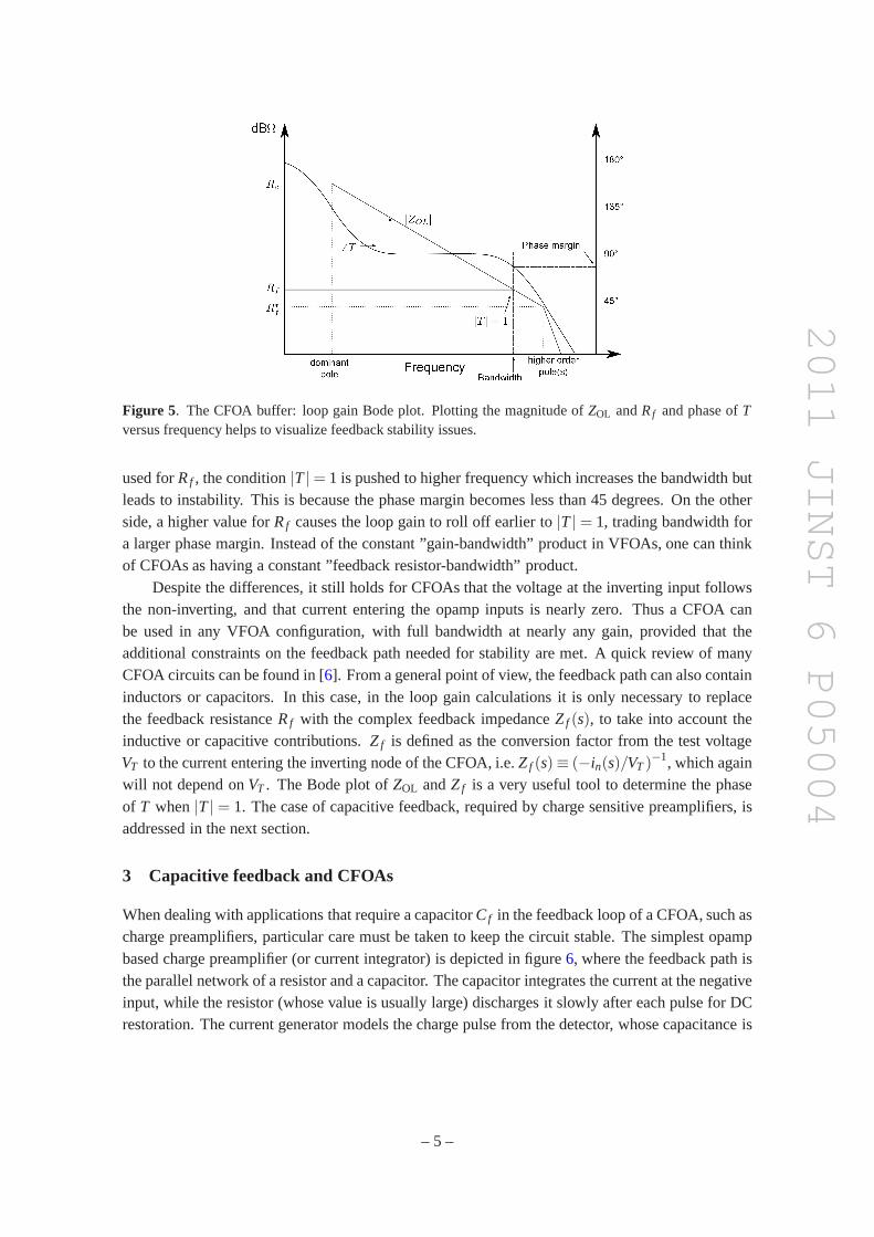
1 , the -180 degrees phase shift cancels the minus sign in2.1 andthe negative gain of the feedback loop becomes positive. When this happens, if|T|> 1 the input isforced to larger and larger values and leads to instability in the feedback loop. On the other side, if|T| < 1 then stability is preserved. Conventionally, a feedback network is considered stable if thephase ofT in |T|= 1, called the ”phase margin”, is larger than 45 degrees. Thisis shown in figure5,where the magnitude ofZOL andRf are plotted (so that|T| = 1 occurs at the crossing between thecurves) as well as the phase ofT, from which the phase margin can be read. If a smaller value is
1Consider a circuit driven by a voltage sourceVin. Let us denote its output byVout(Vin). A circuit is called linear ifVout(aVin) = aVout(Vin), wherea is a real number.
– 4 –
2011 JINST 6 P05004
dB
Frequencydominant
pole
higher order
pole(s)
135°
90°
45°
180°
Figure 5. The CFOA buffer: loop gain Bode plot. Plotting the magnitude of ZOL andRf and phase ofTversus frequency helps to visualize feedback stability issues.
used forRf , the condition|T|= 1 is pushed to higher frequency which increases the bandwidth butleads to instability. This is because the phase margin becomes less than 45 degrees. On the otherside, a higher value forRf causes the loop gain to roll off earlier to|T| = 1, trading bandwidth fora larger phase margin. Instead of the constant ”gain-bandwidth” product in VFOAs, one can thinkof CFOAs as having a constant ”feedback resistor-bandwidth” product.
Despite the differences, it still holds for CFOAs that the voltage at the inverting input followsthe non-inverting, and that current entering the opamp inputs is nearly zero. Thus a CFOA canbe used in any VFOA configuration, with full bandwidth at nearly any gain, provided that theadditional constraints on the feedback path needed for stability are met. A quick review of manyCFOA circuits can be found in [6]. From a general point of view, the feedback path can also containinductors or capacitors. In this case, in the loop gain calculations it is only necessary to replacethe feedback resistanceRf with the complex feedback impedanceZf (s), to take into account theinductive or capacitive contributions.Zf is defined as the conversion factor from the test voltageVT to the current entering the inverting node of the CFOA, i.e.Zf (s)≡ (−in(s)/VT)−1, which againwill not depend onVT . The Bode plot ofZOL andZf is a very useful tool to determine the phaseof T when|T| = 1. The case of capacitive feedback, required by charge sensitive preamplifiers, isaddressed in the next section.
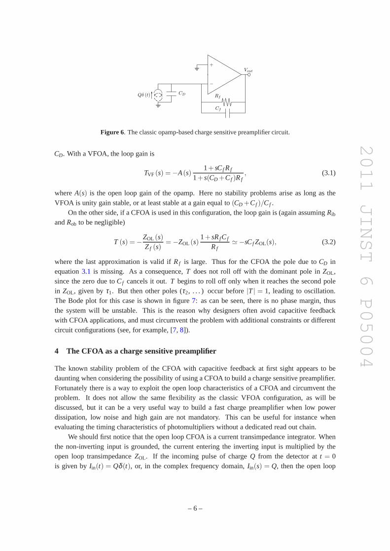
3 Capacitive feedback and CFOAs
When dealing with applications that require a capacitorCf in the feedback loop of a CFOA, such ascharge preamplifiers, particular care must be taken to keep the circuit stable. The simplest opampbased charge preamplifier (or current integrator) is depicted in figure6, where the feedback path isthe parallel network of a resistor and a capacitor. The capacitor integrates the current at the negativeinput, while the resistor (whose value is usually large) discharges it slowly after each pulse for DCrestoration. The current generator models the charge pulsefrom the detector, whose capacitance is
– 5 –
2011 JINST 6 P05004
Figure 6. The classic opamp-based charge sensitive preamplifier circuit.
CD. With a VFOA, the loop gain is
TVF (s) = −A(s)1+sCf Rf
1+s(CD +Cf )Rf, (3.1)
whereA(s) is the open loop gain of the opamp. Here no stability problemsarise as long as theVFOA is unity gain stable, or at least stable at a gain equal to(CD +Cf )/Cf .
On the other side, if a CFOA is used in this configuration, the loop gain is (again assumingRib
andRob to be negligible)
T (s) = −ZOL (s)Zf (s)
= −ZOL (s)1+sRfCf
Rf≃−sCf ZOL(s), (3.2)
where the last approximation is valid ifRf is large. Thus for the CFOA the pole due toCD inequation3.1 is missing. As a consequence,T does not roll off with the dominant pole inZOL,since the zero due toCf cancels it out.T begins to roll off only when it reaches the second polein ZOL, given byτ1. But then other poles (τ2, . . . ) occur before|T| = 1, leading to oscillation.The Bode plot for this case is shown in figure7: as can be seen, there is no phase margin, thusthe system will be unstable. This is the reason why designersoften avoid capacitive feedbackwith CFOA applications, and must circumvent the problem with additional constraints or differentcircuit configurations (see, for example, [7, 8]).
4 The CFOA as a charge sensitive preamplifier
The known stability problem of the CFOA with capacitive feedback at first sight appears to bedaunting when considering the possibility of using a CFOA tobuild a charge sensitive preamplifier.Fortunately there is a way to exploit the open loop characteristics of a CFOA and circumvent theproblem. It does not allow the same flexibility as the classicVFOA configuration, as will bediscussed, but it can be a very useful way to build a fast charge preamplifier when low powerdissipation, low noise and high gain are not mandatory. Thiscan be useful for instance whenevaluating the timing characteristics of photomultipliers without a dedicated read out chain.
We should first notice that the open loop CFOA is a current transimpedance integrator. Whenthe non-inverting input is grounded, the current entering the inverting input is multiplied by theopen loop transimpedanceZOL. If the incoming pulse of chargeQ from the detector att = 0is given byIin(t) = Qδ (t), or, in the complex frequency domain,Iin(s) = Q, then the open loop
– 6 –

2011 JINST 6 P05004
dB
Frequencydominant
pole
higher order
pole(s)
135°
90°
45°
180°
phasemargin!
Figure 7. The classic opamp charge sensitive preamplifier: loop gainBode plot, showing that this configu-ration will not work with a CFOA.
CFOA gives an output signal
Vout(s) = −ZOL(s)Iin(s) = −QRc
1+sRcCcG(s) . (4.1)
PuttingG(s) = 1 as for an ideal CFOA, in the time domain, the preceding expression becomes
Vout(t) = − QCc
exp
(
− tRcCc
)
θ (t) , (4.2)
whereθ(t) is the ideal step function, which equals 0 ift < 0 and 1 otherwise. This signal is a pulsewith zero rise time, instantaneously peaking at a voltage−Q/Cc, then slowly discharging with timeconstantRcCc. With typical values ofRc = 100 kΩ, Cc = 1 pF, the peak amplitude would be 160mV/Me− and the discharge time constantτ f = 100 ns. Since the fall is exponential, the 90% to10% fall time is given by 2.2τ f , or 220 ns with the values above. Figure8 shows the responseof a Texas Instruments OPA695 to a 1 Me− charge injected at the inverting input. Note that themeasurement was taken at the far end of a 50Ω terminated cable, so the measured signal amplitudeis halved. The values estimated from figure8 are aboutCc = 1 pF (from the peak amplitude) andRc = 70 kΩ (from the fall time). These values are in rough agreement with those obtained directlyfrom the plot ofZOL in the OPA695 datasheet. It should be noted thatCc andRc suffer from theinherent lack of precision of integrated resistors and capacitors, which can reach a process spreadof about 30%, whereas discrete passive components are available with much higher precision.
This open loop configuration yields the maximum gain and the fall time achievable with aparticular CFOA in the configuration to be described in the following. A very large feedbackresistor can be used to achieve this condition while stabilizing the DC working point. Incidentally,the OPA695 was found to work even without any feedback resistor, i.e. open loop at DC, but thisis an exception among CFOAs.
Gain and fall time of the open loop configuration can be modified with the circuit shown infigure9. As will be clear after the calculations, the purpose of the feedback resistorRf is to shorten
– 7 –

2011 JINST 6 P05004
0.1 0.2 0.3 0.4 0.5 0.6 0.7 0.8 0.9330
340
350
360
370
380
390
400
410
420
430
time (us)
Vo
ut(m
V)
Figure 8. Voltage pulse from an open loop OPA695 from Texas Instruments with a 1 Me− charge at theinput. The inlay shows the schematic.
x1
x1
Figure 9. The CFOA as a charge sensitive preamplifier.
the fall time with respect to the open loop value, and does notaffect gain nor stability as long asRf ≫ R∗
f . The purpose of the feedback capacitorCf is to decrease gain if necessary. In order tokeep this configuration stable, the resistorRg was put in series with the CFOA input.
First of all, let us consider the stability of this configuration. By calculating the loop gainTfrom figure10, neglectingRib andRob, we obtain
T(s) =VR
VT= −ZOL(s)
Zf (s)= −ZOL(s)
Rf
(
1+s[Cf Rf +(CD +Cf )Rg]
1+s(CD +Cf )Rg
)
. (4.3)
The corresponding Bode plot is depicted in figure11. This expression makes clear the role ofRg
to guarantee stability, providing a zero inZf to compensate the pole at high frequency. As waspointed out in the introduction, feedback is stable as long as |T| < 1 whenZOL reaches its higher
– 8 –

2011 JINST 6 P05004
x1
x1
Figure 10. The CFOA as a charge sensitive preamplifier: circuit diagram for loop gain calculation.
order poles. SinceZOL ≃ R∗f at the frequency of the higher order poles, the stability condition is
a constraint on the minimum value of the feedback impedanceZf at high frequency. In our case,from equation4.3, we have that at high frequency the value of the feedback impedance is
Zf ≃(CD +Cf )RgRf
(CD +Cf )Rg +Cf Rf, (4.4)
which must be larger thanR∗f for stability. Since as we shall see all the other parametersare usually
set by the application requirements, the stability condition becomes a constraint on the minimumvalue ofRg:
Rg >Cf
CD +Cf
Rf R∗f
Rf −R∗f≡ Cf
CD +CfRx. (4.5)
whereRx is defined as the resistance value such that if is put in parallel with a resistor of valueRf ,gives an equivalent resistanceR∗
f , i.e. Rx||Rf ≡ R∗f . AssumingRf to be much larger thanR∗
f , wecan approximateRx ≃ R∗
f , and equation4.5becomes
Rg >Cf
CD +CfR∗
f , (4.6)
regardless of the value ofRf .Let us now calculate the gain expression. From figure9, we have the node equations
−Q+sCDVD +sCf (VD −Vout)+VD
Rg= 0 (4.7)
at the detector node, andVD
Rg+
Vout
RF+
Vout
ZOL(s)= 0 (4.8)
at the CFOA input node, where equation1.1 was used to turn the currentin at the inverting nodeinto the last part of the sum. Solving the system forVout gives
Vout(s) = − Rf ||ZOL(s)
1+s(
Cf (Rf ||ZOL(s))+ (CD +Cf )Rg
)Q. (4.9)
– 9 –

2011 JINST 6 P05004
dB
dominant
pole
higher order
pole(s)
135°
90°
45°
180°
Figure 11. The CFOA as a charge sensitive preamplifier: loop gain Bode plot.
HereRg gives a negligible contribution, as long as its value is keptat the minimum allowed byequation4.6, i.e. if Rg = R∗
fCf /(CD +Cf ). Then equation4.9becomes
Vout(s) = − Rf ||ZOL(s)
1+sCf
(
Rf ||ZOL(s)+R∗f
)Q, (4.10)
which, if Rf ≫ R∗f , and substituting equation1.2for ZOL(s), becomes
Vout(s) = − Rf RcG(s)
Rf +RcG(s)+sRf Rc(Cf G(s)+Cc)Q. (4.11)
Now if we assume thatRc ≫ Rf , and thus letRc → ∞ (otherwise the parallelRf ||Rc should beconsidered in the following equations in place ofRf alone) we obtain
Vout(s) = − Rf
1+sRf (Cf +Cc/G(s))Q. (4.12)
Finally, if we setG(s) = 1, neglecting the high frequency poles of the CFOA, we have
Vout(s) = − Rf
1+sRf (Cf +Cc)Q, (4.13)
which in time domain becomes
Vout(t) = − QCf +Cc
exp
(
− tRf (Cf +Cc)
)
θ (t) . (4.14)
This expression is just like the open loop response of equation4.2, but with a gain given byCf +Cc,and a fall time which is determined byRf instead ofRc.
NeglectingG(s), as in equation4.13, means to assume that the CFOA is ideal, without anybandwidth limitation. This leads to a zero rise time in equation 4.14. When a first order contribution
– 10 –

2011 JINST 6 P05004
from G(s) is taken into account, so that one high frequency pole from equation1.3is introduced inequation4.12, then the frequency response becomes
Vout(s) = − Rf
1+sRf (Cf +Cc)+s2RfCcτ1Q. (4.15)
The denominator now has two poles very far from each other. One is approximately located at
p′ =1
Rf (Cc +Cf ), (4.16)
as for the ideal case given in equation4.13, while the other is located at higher frequency:
p′′ =Cf +Cc
Ccτ1. (4.17)
The higher frequency pole gives the time constant associated with the rise time of the output pulse,which is basicallyτ1. Equation4.17suggests that the rise time could be lowered by increasingCf .However, higher order poles (τ2, . . . ) have been neglected in that calculation, as well as theslewrate limitations of the CFOA, so the time constant can hardlybe less thanτ1 in any case. Since therise is exponential, the 10% to 90% rise time is given by 2.2τ1.
The value ofτ1 can be estimated from the open loop transimpedance plot or from the maximumbandwidth of the CFOA, both to be found in the datasheet. An important fact should be pointedout here: when manufacturers claim in a CFOA datasheet that the bandwidth exceeds 1 GHz, theyoften mean that such a speed can be achieved in the buffer configuration via a small phase margin,i.e. via a controlled amount of peaking in the frequency response. The second pole of the CFOAis often located one or two octaves lower, as can be seen from the position of the higher orderpoles in the plot of the open loop transimpedance. We observed this in many commercial CFOAs,whose high order poles sit around 400 MHz, but can be used in buffer configuration up to 1 GHzand above by reducing the phase margin to less than 30 degrees. If the second pole is located atf1 = 400 MHz, thenτ1 ≃ 0.4 ns, and so the rise time in response to the charge pulse turns outto beabout 1 ns.
So far we have neglected the output impedances of the input and output buffers, which wedenoted byRib andRob respectively. Their values are very small, however they canhave an impacton stability. By equation4.5, if Cf is not used, then there is no need forRg. This is not true anymoreif the effect ofRib is considered. If the detector capacitanceCD is large enough, then an additionalpole in T can occur at frequency 1/2πRibCD. This leads to additional phase shift and instabilityin the feedback loop unlessRf is large enough to let this additional pole fall out of the bandwidthof the amplifier. A smallRg can compensate this pole: in this case the loop gain withCf = 0 isapproximately given by
T(s) = −ZOL(s)Rf
1+sCDRg
1+sCD(Rg +Rib). (4.18)
It is clear from this expression that even whenCf is zero a smallRg of about 25 to 50Ω should beused to assure the stability of the system.
A similar effect can be produced byRob and the series combination ofCf andCD by introduc-ing a pole at the output with feedback taken viaRf . The calculations in this case, neglectingRib,
– 11 –
2011 JINST 6 P05004
0.1 0.2 0.3 0.4 0.5 0.6 0.7 0.8 0.9100
150
200
250
300
350
time (us)
Vo
ut(m
V) Cf = 0 pF
Cf = 1.8 pF
Cf = 5 pF
Figure 12. Voltage pulses from an AD8001 from Analog with a 5 Me− charge at the input, with differentvalues of feedback capacitanceCf .
give the approximate result (forRob ≪ Rg,Rf )
T(s) = −ZOL(s)Rf
1+s[Cf Rf +(CD +Cf )Rg]
1+s(CD +Cf )Rg +s2CDCf RgRob. (4.19)
This expression shows an additional pole at high frequency,due toRob, which can lead to instability.This problem was observed both in the OPA695 from TI and in theLMH6702 from National, butnot in the AD8001 from Analog, which is slightly slower, so that the pole fell out of the bandwidthof the amplifier. To circumvent this problem, a small resistor Rh should be put in series withCf todecouple the capacitive load from the output of the CFOA and add a zero to compensate the pole.The loop gain, evaluated in the case whereRh,Rob ≪ Rg,Rf for conciseness, becomes
T(s) = −ZOL(s)Rf
1+s[Cf Rf +(CD +Cf )Rg]+s2CDCf RhRob
1+s(CD +Cf )Rg +s2CDCf (Rg +Rh)Rob. (4.20)
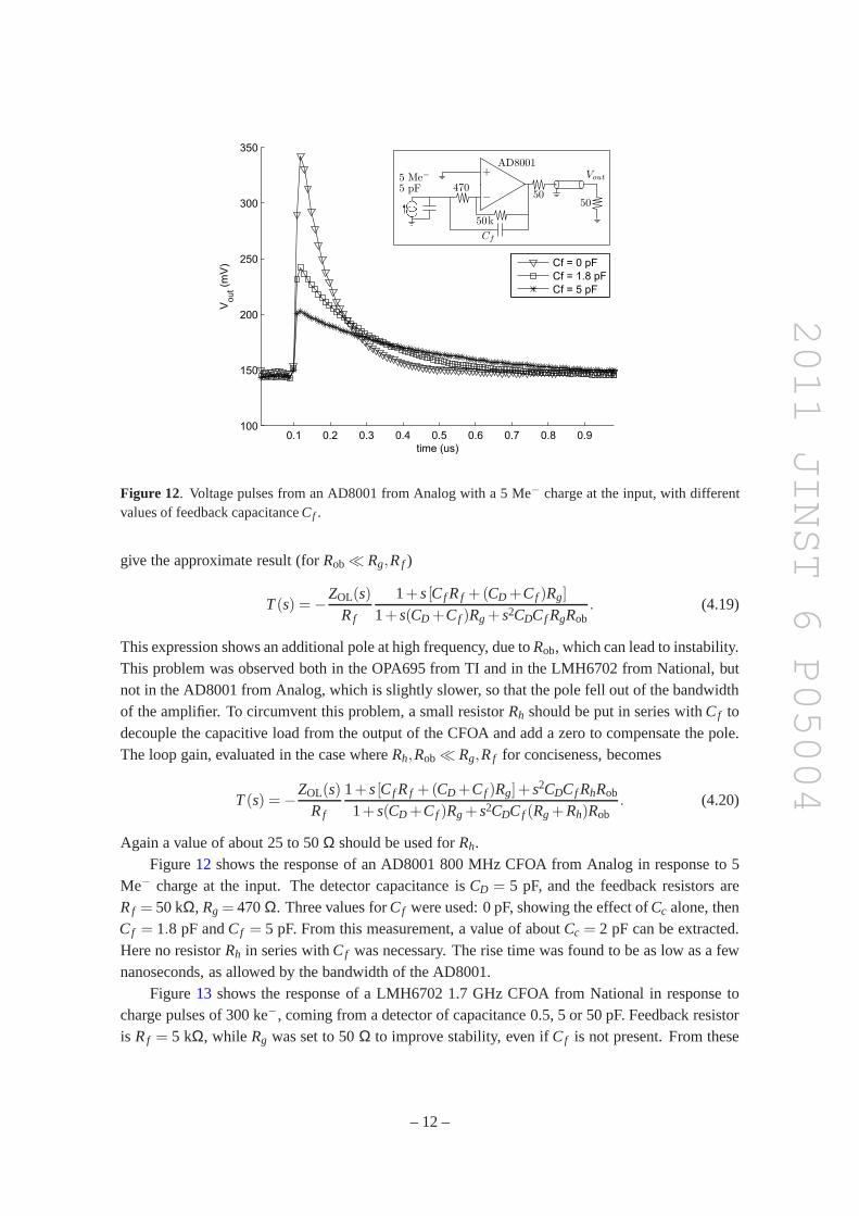
Again a value of about 25 to 50Ω should be used forRh.Figure12 shows the response of an AD8001 800 MHz CFOA from Analog in response to 5
Me− charge at the input. The detector capacitance isCD = 5 pF, and the feedback resistors areRf = 50 kΩ, Rg = 470Ω. Three values forCf were used: 0 pF, showing the effect ofCc alone, thenCf = 1.8 pF andCf = 5 pF. From this measurement, a value of aboutCc = 2 pF can be extracted.Here no resistorRh in series withCf was necessary. The rise time was found to be as low as a fewnanoseconds, as allowed by the bandwidth of the AD8001.
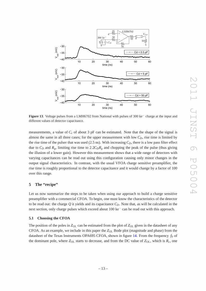
Figure13 shows the response of a LMH6702 1.7 GHz CFOA from National in response tocharge pulses of 300 ke−, coming from a detector of capacitance 0.5, 5 or 50 pF. Feedback resistoris Rf = 5 kΩ, while Rg was set to 50Ω to improve stability, even ifCf is not present. From these
– 12 –
2011 JINST 6 P05004
10 20 30 40 50 60−40
−35
−30
time (ns)
Vo
ut(m
V)
Cd = 0.5 pF
10 20 30 40 50 60−40
−35
−30
time (ns)
Vo
ut(m
V)
Cd = 5 pF
10 20 30 40 50 60−40
−35
−30
time (ns)
Vo
ut(m
V)
Cd = 50 pF
Figure 13. Voltage pulses from a LMH6702 from National with pulses of 300 ke− charge at the input anddifferent values of detector capacitance.
measurements, a value ofCc of about 3 pF can be estimated. Note that the shape of the signal isalmost the same in all three cases; for the upper measurementwith low CD, rise time is limited bythe rise time of the pulser that was used (2.5 ns). With increasingCD, there is a low pass filter effectdue toCD andRg, limiting rise time to 2.2CDRg and chopping the peak of the pulse (thus givingthe illusion of a lower gain). However this measurement shows that a wide range of detectors withvarying capacitances can be read out using this configuration causing only minor changes in theoutput signal characteristics. In contrast, with the usualVFOA charge sensitive preamplifier, therise time is roughly proportional to the detector capacitance and it would change by a factor of 100over this range.
5 The “recipe”
Let us now summarize the steps to be taken when using our approach to build a charge sensitivepreamplifier with a commercial CFOA. To begin, one must know the characteristics of the detectorto be read out: the chargeQ it yields and its capacitanceCD. Note that, as will be calculated in thenext section, only charge pulses which exceed about 100 ke− can be read out with this approach.
5.1 Choosing the CFOA
The position of the poles inZOL can be estimated from the plot ofZOL given in the datasheet of anyCFOA. As an example, we include in this paper theZOL Bode plot (magnitude and phase) from thedatasheet of the Texas Instruments OPA695 CFOA, shown in figure 14. From the frequencyf0 ofthe dominant pole, whereZOL starts to decrease, and from the DC value ofZOL, which isRc, one
– 13 –
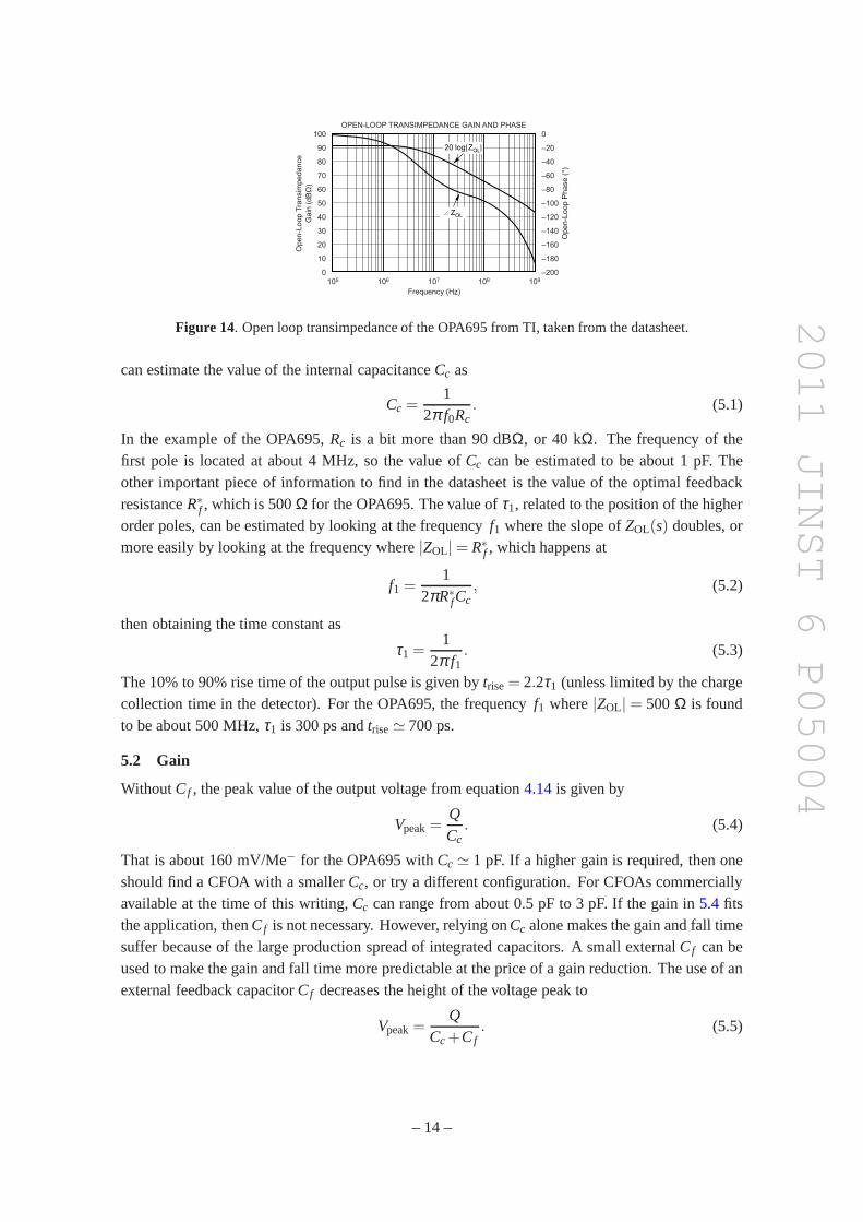
2011 JINST 6 P05004
100
90
80
70
60
50
40
30
20
10
0
0
–20
–40
–60
–80
–100
–120
–140
–160
–180
–200
105 106 107 108 109
OPEN-LOOP TRANSIMPEDANCE GAIN AND PHASE
Frequency (Hz)O
pe
n-L
oop
Tra
nsim
pe
da
nce
Ga
in (
dB
Ω)
Op
en-L
oop
Ph
ase (
°)
20 log|ZOL|
∠ZOL
Figure 14. Open loop transimpedance of the OPA695 from TI, taken from the datasheet.
can estimate the value of the internal capacitanceCc as
Cc =1
2π f0Rc. (5.1)
In the example of the OPA695,Rc is a bit more than 90 dBΩ, or 40 kΩ. The frequency of thefirst pole is located at about 4 MHz, so the value ofCc can be estimated to be about 1 pF. Theother important piece of information to find in the datasheetis the value of the optimal feedbackresistanceR∗
f , which is 500Ω for the OPA695. The value ofτ1, related to the position of the higherorder poles, can be estimated by looking at the frequencyf1 where the slope ofZOL(s) doubles, ormore easily by looking at the frequency where|ZOL| = R∗
f , which happens at
f1 =1
2πR∗fCc
, (5.2)
then obtaining the time constant as
τ1 =1
2π f1. (5.3)
The 10% to 90% rise time of the output pulse is given bytrise = 2.2τ1 (unless limited by the chargecollection time in the detector). For the OPA695, the frequency f1 where|ZOL| = 500Ω is foundto be about 500 MHz,τ1 is 300 ps andtrise≃ 700 ps.
5.2 Gain
WithoutCf , the peak value of the output voltage from equation4.14is given by
Vpeak=QCc
. (5.4)
That is about 160 mV/Me− for the OPA695 withCc ≃ 1 pF. If a higher gain is required, then oneshould find a CFOA with a smallerCc, or try a different configuration. For CFOAs commerciallyavailable at the time of this writing,Cc can range from about 0.5 pF to 3 pF. If the gain in5.4 fitsthe application, thenCf is not necessary. However, relying onCc alone makes the gain and fall timesuffer because of the large production spread of integratedcapacitors. A small externalCf can beused to make the gain and fall time more predictable at the price of a gain reduction. The use of anexternal feedback capacitorCf decreases the height of the voltage peak to
Vpeak=Q
Cc +Cf. (5.5)
– 14 –
2011 JINST 6 P05004
5.3 Fall time
The time constant of the exponential discharge is given by(Cf +Cc)(Rf ||Rc). The 90% to 10%fall time of the output pulse is thus given bytfall = 2.2(Cf +Cc)(Rf ||Rc). If Rc is large enough,then the fall time is determined byRf alone, which can be chosen to give the required fall time:
Rf =tfall
2.2(Cf +Cc). (5.6)
The value forRf should in any case be bigger thanR∗f , to guarantee stability, and smaller thanRc.
If Rf is larger thanRc, then the fall time is set byRc and the only purpose ofRf is to stabilizethe DC working point. This should in any case guarantee enough freedom: in the example of theOPA695, withCc = 1 pF,Rc = 40 kΩ, R∗
f = 500Ω, assumingCf = 0, Rf can range from about 1kΩ, which yields a 3 ns fall time, to infinity, which yields about100 ns fall time since in this casethe discharge is onRc alone, as in the open loop case.
5.4 Stability
After settingCf andRf , one should chooseRg from equation4.6to guarantee stability:
Rg =Cf
CD +CfRx, (5.7)
whereCD is the detector capacitance and
Rx ≡Rf R∗
f
Rf −R∗f. (5.8)
Even if Cf is not used, a smallRg of about 25 to 50Ω should be used, at least with the fastestCFOAs, to compensate the pole given byCD with the input buffer output resistanceRib. Also asmall Rh of about the same value should be put in series withCf to compensate the pole due todirect capacitive load at the output of the CFOA.
6 Noise performance and equivalent noise charge
Let us now suppose there is a shaping filter after the preamplifier, a common practice in detectorread out to improve the noise performance of the read out chain. The shaper makes it necessaryin our calculations to convert the noise sources of the preamplifier, which are expressed in termsof power spectra, to the so-called ”equivalent noise charge” (ENC). ENC is the amount of chargefrom the detector for which the signal equals the noise and below which no charge pulse can bedetected [9, 10].
For the sake of simplicity, let us assume the shaping filter tobe of the simple CR-RC type,with time constantτ , thus giving a transfer function
F(s) =sτ
(1+sτ)2 , (6.1)
whereτ has to be smaller than the preamplifier discharge constant(Cf +Cc)(Rf ||Rc), and largerthan the higher order zero ofZf at frequency 1/2πRg(CD +Cf ). These conditions guarantee that
– 15 –

2011 JINST 6 P05004
Figure 15. The CFOA charge sensitive preamplifier: full read out chainwith preamplifier and shaper,including noise sources of the preamplifier.
at frequencies near 1/2πτ the charge sensitive preamplifier behaves like an ideal integrator. Inall following calculations we will consider the CFOA to be ideal, and since the shaper filters allfrequencies far from 1/2πτ , we can approximate equation4.13as
Vout(s) = − Rf
1+sRf (Cf +Cc)Q≃− 1
s(Cf +Cc)Q, (6.2)
which in time domain becomes a step:
Vout(t) ≃− QCf +Cc
θ (t) . (6.3)
The output voltage pulse of the whole chain in response to a chargeQ in t = 0 is
Vout(s) = − Qs(Cf +Cc)
F(s) = − τ(1+sτ)2
QCf +Cc
, (6.4)
which in time domain becomes
Vout(t) = − QCf +Cc
tτ
exp(
− tτ
)
θ(t). (6.5)
The read out chain comprised of the preamplifier and the idealshaper is depicted in figure15,which shows also the main noise sources in the preamplifier: the CFOA itself, with its voltage andcurrent contributionsea(s) andia(s), and the thermal contributions of resistorsRg andRf , modeledas current generatorsig(s) and i f (s). Since we are dealing with high frequency applications, weassume all the low frequency (flicker) noise contributions to be negligible, and all noise generatorsto have a constant power spectral density.
In the first place, let us calculate the voltage at the output due to the noise sources, one at atime. From the node equations, and with the same approximations onZOL that led to equation4.13,it can be shown that the noise due toRg gives at the output of preamplifier
Vig(s) =s(CD +Cf )RgRf
1+s(Cf +Cc)Rfig(s) ≃
CD +Cf
Cf +CcRgig(s), (6.6)
while noise fromRf gives
Vi f (s) =(1+s(CD +Cf )Rg)Rf
s(Cf +Cc)Rfi f (s) ≃
1s(Cf +Cc)
i f (s). (6.7)
– 16 –

2011 JINST 6 P05004
Current noise from the amplifier has the same transfer function asi f (s), so it is given by
Via(s) ≃1
s(Cf +Cc)ia(s). (6.8)
and finally for the voltage noise of the amplifier
Vea(s) =1+s(CD +Cf )(Rg +Rf )
(Cf +Cc)Rfea ≃
CD +Cf
Cf +Ccea. (6.9)
It is clear thatea andRgig ≡ eg share the same transfer function:Rg gives a voltage or ”series”noise contribution, likeea, while Rf gives a current or ”parallel” noise contribution, likeia.
The noise at the output of the full chain due to each contribution is given by the above expres-sions multiplied by the shaper transfer functionF(s):
Vseries(s) =CD +Cf
Cf +CcF(s)eseries(s) (6.10)
for the series noise contributions, and
Vparallel(s) =F(s)
s(Cf +Cc)iparallel(s) (6.11)
for the parallel noise contributions. To obtain the squaredr.m.s. output noise, one must puts= iωin the above expressions, take the mean squared amplitude, and integrate over frequency. For theseries noise,
|Vseries|2 =
(
CD +Cf
Cf +Cc
)2
|ea|21
2π
∫ ∞
0dω |F(iω)|2 , (6.12)
and since1
2π
∫ ∞
0dω |F(iω)|2 =
12π
∫ ∞
0dω
ω2τ2
(1+ ω2τ2)2 =18τ
(6.13)
the series output noise becomes
|Vseries|2 =
(
CD +Cf
Cf +Cc
)2 |ea|28τ
, (6.14)
giving thus a contribution which is inversely proportionalon the shaping time. On the other side,for the parallel noise,
∣
∣Vparallel∣
∣
2=
(
1Cf +Cc
)2
|ia|21
2π
∫ ∞
0dω
∣
∣
∣
∣
F(iω)
iω
∣
∣
∣
∣
2
, (6.15)
and since1
2π
∫ ∞
0dω
∣
∣
∣
∣
F(iω)
iω
∣
∣
∣
∣
2
=τ2
2π
∫ ∞
0dω
1
(1+ ω2τ2)2 =τ8
(6.16)
the parallel output noise becomes
∣
∣Vparallel∣
∣
2=
(
1Cf +Cc
)2 τ |ia|28
, (6.17)
– 17 –

2011 JINST 6 P05004
Figure 16. A basic CFOA circuit: current noise from Q1 can be modeled asa voltage noise in series with thebase of Q1 (as common practice), i.e. at the non-inverting input, while current noise from the polarizationtransistor Q2 is a current source at the inverting input. Other noise sources from transistors inside the CFOAwere neglected.
giving a contribution which is directly proportional to theshaping time. All the contributions mustbe added together in quadrature to give a total output noise
|Vtot|2 = |Vseries|2 +∣
∣Vparallel∣
∣
2=
(
1Cf +Cc
)2(
τ8
(
|ia|2 + |i f |2)
+(CD +Cf )
2
8τ(
|ea|2 + |eg|2)
)
.
(6.18)We can now calculate the equivalent noise charge by dividingthe output noise voltage by thegain from input to output. The gain for a chargeQ at the output of the preamplifier is given byequation6.5, whose peak value isQ/e(Cf +Cc), wheree≃ 2.72 is Euler’s number. The ENC isthus given by
ENC= e(Cf +Cc) |Vtot| =e
2√
2
√
τ(
|ia|2 + |i f |2)
+(CD +Cf )2
τ(|ea|2 + |eg|2). (6.19)
This quantity must be compared with the chargeQ from the detector, and should be at least a factorof 10 or 20 belowQ for a decent signal to noise ratio.
If the integrator time constant cannot be considered much bigger than the filter time constant,i.e. if τ ≃ (Cf +Cc)(Rf ||Rc), the calculations are a bit more complicated, and the effectis similarto that of a CR2-RC shaping filter. If this is the case, the coefficients in equation 6.19should bemodified accordingly, leading to a slightly higher noise charge.
Let us now evaluate the ENC for a typical configuration withCD = CF = 3 pF, RF = 20kΩ, Rg = 500 Ω, for a OPA695 from Texas Instruments. The parallel noise ofRf is given by∣
∣i f∣
∣
2= 4kBT/Rf ≃ 1 pA/
√Hz (wherekB is the Boltzmann constant, andT is temperature, which
we assume to be 300 K). The series noise ofRg is given by|eg|2 = 4kBTRg ≃ 3 nV/√
Hz . Fromthe OPA695 datasheet we find the series noise of the opamp to be|ea| ≃ 1.7 nV/
√Hz and its
current noise at the inverting input to be|ia| ≃ 22 pA/√
Hz. The overall noise is largely dominatedby this last contribution. With a short shaping time ofτ = 5 ns, to minimize the weight of thecurrent noise and to exploit the wide bandwidth of the CFOA, the equivalent noise charge given
– 18 –

2011 JINST 6 P05004
by equation6.19is about 6 ke− r.m.s., dominated by|ia|. This yields a f.w.h.m. noise of about 15ke−. On the other side, the contribution of the series noise is less than 1 ke− r.m.s., always quitenegligible when compared to the parallel part, unless the detector has a very large capacitance. Alonger shaping time worsens things a bit, since the parallelpart of the ENC is proportional to
√τ,
and would possibly make the use of a CFOA not preferable compared to the slower but less noisyVFOA-based configuration.
Even if the exact values depend on the specific CFOA model, we found all CFOAs to haveabout the same current noise at the inverting input, about 20pA/
√Hz. This is the main limit on the
noise performances of this configuration, and makes it useful to read out charges of only about 100ke− or more. The reason for this lies in the fact that the negativeinput of the CFOA is canonicallyconnected to the emitter or source of the transistors of the input stage. Figure16 shows a basicCFOA circuit: it can be seen that the input signal at the inverting node has to be directly comparedto the shot noise from the current source for the input transistor. This current can be as high as 1 mAfor high frequency operation, giving|ia| ≃ 20 pA/
√Hzof shot noise. Thus, this configuration will
provide an adequate signal to noise ratio only in case of highenergy radiation or in case the detectoris some sort of photomultiplier (where a charge of the order of 1 Me− is expected). Unfortunately,it will not fit the noise requirements of other kinds of detectors which yield smaller charge signals.
References
[1] S. Franco,Current-feedback amplifiers, in Analog circuit design: art, science and personalities, J.Williams ed., Butterworth Heinemann, U.S.A. (1991), chapter 25.
[2] National Semiconductor,Current-feedback myths debunked, OA-20 (1992).
[3] National Semiconductor,Current feedback amplifiers, OA-31 (1992).
[4] G. Palumbo and S. Pennisi,Current-feedback amplifiers versus voltage operational amplifiers,IEEE Trans. Circuits Syst.48 (2001) 617.
[5] S. Franco,Design with operational amplifiers and analog integrated circuits, McGraw-Hill, U.S.A.(2002), see pages 347-397.
[6] National Semiconductors,Current feedback op amp applications circuit guide, OA-07(1988).
[7] J. Mahattanakul and C. Toumazou,A theoretical study of the stability of high frequency currentfeedback op-amp integrators, IEEE Trans. Circuits Syst.43 (1996) 2.
[8] B. Maundy, S.J.G. Gift and P.B. Aronhime,A novel differential high-frequency CFA integrator,IEEE Trans. Circuits Syst. II51 (2004) 289.
[9] E. Gatti and P. Manfredi,Processing the signals from solid-state detectors in elementary-particlephysics, Nuovo Cim.9 (1986) 1.
[10] V. Radeka,Low-noise techniques in detectors, Ann. Rev. Nucl. Part. Sci.38 (1988) 217.
– 19 –